Embed Size (px)
Citation preview
SELF~TIMED VLSI SYSTEMS
Charles L. Seitz
Department of Computer Science California Institute of Technology
Abst ract & I nt r oduction
This short paper is intended to explain why the subject of self-timed logic is relevant to a conference on VLSI.
345
Scaling down feature s~ze and scaling up chip area not only increases the complexity of chips, but also changes relationships in the parameters which describe the physical characteristics of switching devices, circuits, and wires. The physical change which most impacts the design disciplines employed for VLSI -- particularly the timing aspect of design -- is the increased wire delay associated with the increased resistivity of scaled down wires. Wires that run even a small fraction of the way across a chip will impose a significant delay . Clock distribution and long-distance communication required by synchronous systems will become problematic. Otherwise, it appears that the timing aspect of design for submicron feature size circuits will generally resemble that of today's MOS technology, in that delays will be largely determined by parasitic wiring capacitance .
A general introduction and outline of the self-timed discipline of digital system design (by this author) is to be published in Chapter 7 of [1], and to which the reader is referred for more detail. Briefly, the selftimed discipline is concerned with complexity management, and with timing of digital systems under conditions in which delays between parts are large or uncertain. The amount of circuitry that can be fabricated onto a single chip is increasing to well beyond that point at which informal complexity management disciplines are effective. The escalation of complexity suggests for VLSI design a rigorous discipline of modularity. The large long-distance communication delays suggest in addition that the modules be independently timed. This is the central idea of self-timed systems : it is a discipline in which each system "part" keeps time to itsel f. Those "parts" of a selftimed system whose correct operation must be certified by appealing to time and physical argument are called elements. Otherwise, self-timed systems are constructed (defined recursively) as restricted classes of interconnections of self-timed systems or elements, and correct sequential operation is independent of the delays in the interconnections.
Scaling ~crocircuit Timing
A basic reference on the physical consequences of scaling feature size is Introduct ion to ~SI Systems (1] by Carver Mead and Lynn Conway, or the article [2] by Amr Mohsen in the first section of these Proceedi ngs.
What is meant here by digital system "timing" is the wav in which the
This research was supported by the Defense Advanced Research Projects Agency (ARPA) under contract number N00123-78-C-0806.
CALTECH CONFERENCE ON VLSI , J a nuary 197 9
346 Cha rles L . Se i tz
physical, metric notion of time is connected to a sequential process. The correct operation and performance of a switching system depends upon the values of and tolerances on:
(1) the switching delay of the elementary switching devices,
(2) the additional delay induced on the switching devices by attaching wires to them and incorporating them into circuits, and
(3) the delay associated with equalizing the potential across wires.
Scaling feature size shifts many of the physical parameters which determine these delays. The scaling effects discussed in some detail below are those that appear to have a major impact on timing and design disciplines, and are too fundamental to be circumvented entirely by process "fixes."
MOS Switches and Circuits
As indicated in the references [1,2] cited above, sensible scaling of MOS technology holds electric fields constant, so that power and signal voltages scale down with the minimum feature size. The lithography directly determines the minimum gate length of the MOS transistor, so the transit time of this switch and currents also scale down in proportion to the feature size. Even though smaller MOS devices are proportionately faster, power per device scales down quadratically, and power per unit area remains constant . These general scaling rules apply to MOS parts in which performance is an issue. Of course, some applications trade speed and power in favor of reduced power consumption, and so operate at lower voltages.
Switching energy, the product of the device power and its delay time, is a fundamental figure of merit which relates the cost of a computation to this parameter of the switching devices which perform the computation. The switching energy for MOS technologies scales down as the third power of the feature size, so the general physical consequence of reduced feature size is highly desirable. The only unfavorable effect of this scaling for the switches relates to the reduced operating voltages decreasing gain and increasing subthreshold current. These characteristics are exponentially dependent on the ratio of signal voltages to kT/q, and so could be brought into line by operating circuits at reduced temperature. Dynamic storage requires small subthreshold currents and presently places the upper bound on many timing relations. Although dynamic registers will continue to be an important MOS circuit trick, scaling will reduce the refresh period to the extent that the dynamic random-access storage devices used so widely today will become unworkable and replaced with static designs.
What is generally left out of such discussions of the consequences of scaling on the switches is the following important characteristic of MOS technology: If an entire MOS circuit or system is scaled down -- switches, wires, voltages, and all-- its timing behavior scales essentially with that of the switches. We mention as exceptions only that the scaling must be such that wires can still reasonably be regarded as equipotentials and increased subthreshold currents do not discharge dynamically stored information.
Consider the process of scaling a MOS circuit such as an adder or PLA. Assume that the physical structure is shrunk in all three dimensions, not
SELF-TIW~D LOGIC SESSION

Se l f -Timed VLS I Syst ems 34 7
just in the plan view of the circuit, but in the thickness of the various conductive and insulative layers as well. This form of scaling maintains the same relative surface flatness for the lithographic process, and preserves the electric field geometries of the original circuit. When one of the wires internal to the circuit is shrunk, its (charge-carrying surface) area scales down quadratically while its separation from substrate and from other conductors scales down linearly. So, the capacitance of the scaled down wire scales down linearly. Of course, so too does the gate capacitance scale down linearly. Please note for future purposes that the capacitance per unit length of a minimum dimension wire remains constant in the scaling.
Now, if each wire in the scaled down circuit has its capacitance scaled down linearly, and the current from the switches also scales down linearly, the time rate of change of voltages should remain reasonably constant in the scaling. However, the voltages, hence the voltage difference between logic zero and one, also scales down linearly, so the time required to accomplish a voltage transition between logic zero and one scales down linearly with the reduced feature size and with the transit time of the MOS switches.
Accordingly, smaller MOS circuits and systems are also proportionately faster temporal replicas of today's designs, just as the switches are, but for the possible exceptions mentioned above.
Bipolar Switches and Circuits
The bipolar transistor is normally built up vertically through a sequence of diffusions. The area of the base of each transistor is defined by the lithography, but the thickness of the base is determined by the difference between diffusions, and has for years been about as thin as possible. Fixed base thickness implies that voltages in scaled bipolar circuits could remain the same as those presently in use (but it appears that only those circuit families which use small signal voltage changes will be used in VLSI designs) • The bipolar junction produces a maximum "on 11 current density perpendicular to the surface of the chip, so a reduction in minimum feature size produces a quadratic reduction in base area and in current for the minimum dimension transistor. So again, this scaling produces a quadratic reduction with feature size in the power per device, and constant power per unit area. However, the switches are no faster, and the switching energy improves only quadratically.
The current available from bipolar switches is today in a favorable relationship with the wiring capacitance, but this situation worsens as feature size is reduced. Since the currents scale down quadratically in any scaled circuit, while voltage changes remain fixed, wiring capacitance would have to drop quadratically with feature size just to maintain the same performance. However, since one cannot expect the capacitance of an internal circuit wire to scale down faster than linearly as the circuit is shrunk, scaled down bipolar circuits and systems can be expected to become slightly slower with smaller feature size. Of course, the increased significance of parasitics for bipolar circuits with smaller feature size may be offset by improved layouts or processes.
CALTECH CONFERENCE ON VLSI, January 1979

348 Cha r les L. Seitz
SignaL Energetics While it is usually defined as the product of the device power and
delay time, the switching energy is also proportional to the energy that is required to change the state of a switch input . Reducing the switching energy generally reduces the cost of performing a computation, in that it reflects a reduction in the resources (energy, area) or time required. The reduction of feature size is a very direct approach to reducing the cost of a computation by reducing the switching energy, but equally significant is the reduction in wire size and parasitic energy .
The difference in significance of scaling parasitic delays in MOS and bipolar technologies can also be deduced from an energetics viewpoint. When voltage, current, and transit time all scale down linearly with the minimum feature size dimension as they do in the form of MOS scaling discussed here, the switching energy then scales down as the third power of the feature size. One can reach the same conclusion from the energy stored on the gate of a MOS transistor varying as its capacitance, which scales down linearly, times the square of the voltage. The energy associated with the parasitic capacitance of wires scales in exactly the same way -- indeed, the gate is part of a wire --, which accounts for the temporal behavior of aMOS circuit scaling exactly with that of the switches. What happens in the scaling of bipolar technology is that the switching energy scales down quadratically, as was described in the previous section, and which can be seen also from the capacitance of the bipolar transistor base scaling down quadratically with its area while the voltages remain fixed. The relatively increased significance of parasitic capacitances and energies is that thev scale down only linearly.
Whether of MOS or bipolar technology, the same scaling down of the physical dimensions and switching energies that reduces the cost of performing a computation also creates a large disparity between the internal signal energies and those required at package pins. The driver circuits which must be used to increase signal energy levels at the package pins introduce an exceptional cost in the communication between chips, both in area and in delay (not to mention packages, lead-bonding, etc.). Given a particular transistor characteristic, the minimum driver delay varies as the (natural) log of the ratio of output and input signal energies [1] . This ratio is today typically 100 to 1000, for which the log is in the range 4.5 to 7 (repre~enting the optimum number of stages in the driver). Another factor of 10 to 100 in this ratio, the expected consequence of reducing internal signal energies, will not make a dramatic difference in optimum driver delay, because of the logarithmic dependence. This relationship may explain why little attention has been given to chip packaging schemes which reduce interchip interconnect capacitance. Today's pin driver circuits are a compromise between area and delay, and it is not clear whether delay or area will be more precious in the future.
The pin-driving problem scales somewhat differently for MOS and bipolar technologies. In MOS technology, in which one expects the signal voltage changes at package pins to s cale down as they do internally, the energy required to switch the binary voltage on a package pin of given capacitance scales down quadratically with feature size. Thus the ratio of package pin to internal signal energies scales up linearly, and one would expect a
SELF-TIMED LOGIC SESS ION
Self-Timed VLSI Syst e ms 349
modest increase in the delay imposed by an optimum driver, relative to transit time. However, MOS transit times decrease in the scaling, so the absolute delay of a pin driver circuit can be expected to decrease, although not quite with the transit time. In bipolar technology, in which one expects the signal voltage changes cannot be reduced to less than the several tenths of a volt changes now used in those circuit families showing smallest switching energies, the package pin signal energies remain constant while the internal signal energies scale down quadratically, or perhaps only linearly when dominated by the energy required to drive parasitic wiring. Thus the impact of scaling on pin-driver delay is slight in both the relative and absolute senses.
The Submicron Technology
Although MOS technology benefits more from scaling down feature size than does bipolar technology, it should be understood that MOS started its development from an inferior position in the physical measures of its switching devices. At minimum feature size much above one micron, the two technologies show very different strong points, which have helped to distinguish their areas of principal application. Bipolar technology exhibits superior performance, measured either in speed or in switching energy, and relative insensitivity of circuit operation to wiring capacitance and layout. Some design strategies that today work well for bipolar and poorly for MOS, such as the standard-cell, master-slice, or other techniques which depend on automatic placement and routing, have determined the dominance of bipolar technology in mainframes as much for project management as for performance reasons. Meanwhile, MOS technology has exploited the advantages of a cheaper process, simpler circuits, and higher density, to dominate the high-volume, high-complexity applications including particularly storage, microprocessors, and consumer electronics such as watch and calculator chips. Relatively poor performance and the need for handcrafted design appears to be tolerable in this arena.
What happens as the fabrication technology moves to submicron feature sizes is a convergence of the physical and design characteristics of the two technologies. MOS switches attain the excellent physical characteristics of their bipolar counterparts, while bipolar circuits acquire the design problem of sensitivity of circuit operation to parasitic capacitance and layout for which MOS is infamous. There may well be only one submicron technology. The choice of MOS or bipolar switches will have much less effect on design and application characteristics than, for example, whether two or three levels of metal interconnect are used. The analysis above concerning the scaling of MOS circuits indicates that the timing characteristics of the submicron technology will closely resemble those of today's MOS circuits, in that circuit delays are determined mostly by parasitic capacitance -- hence, the length -- of interconnects. The observation of Sutherland and Mead in [3), that it is the wires rather than the switching elements that dominates the cost (area and energy) and performance limitations of microcircuits, is particularly apt for the submicron technology.
CALTECH CONFERENCE ON VLSI, January 1979

3 50 Charl es L . Se it z
Diffusion De'"lay in Wires
Wires introduce still another kind of performance lLmitation as microcircuit technology is scaled to submicron dimensions. All wires have a nonzero resistivity at ordinary temperatures. This parasitic resistance combined with the parasitic capacitance of the wire limits how well the wire approximates an equipotential. A signal driven onto a wire at one point becomes delayed and its transition time degraded progressively at points more distant from the driven point . The way in which the potential equalizes across the length of a resistive wire is governed by a diffusion equation:
RC dV/dt
where V is the potential on the wire as a function of both time (t) and position (x), and Rand Care the resistance and capacitance per unit length (the same units in which xis measured). Heat conduction in solids is an example of another diffusion process. The potential equalizes by diffusion along a wire in the same way in which the temperature equalizes across a heat conductor. One can see intuitively that the rate at which a voltage or temperature step propagates decreases with distance from the driven point. The time required for the midpoint of the step to reach a distance x
is just RCx2 , and the step is also "smeared out" in time in proportion to the square of the distance.
As indicated in figure 1, the propagation of signals on wires is limited over short distances by the rate of electromagnetic propagation and over
. long distances by diffusion. Please .notice that-- to · first order, neglecting fringing -- the wire delay is independent of wire width, since the smaaler resistivity due to larger cross-section is just balanced by increased capacitance from larger width. The diffusion delay depends on the material resistivity, wire cross-section, and capacitance. What is the magnitude of these delays today, and how do they scale?
Polysilicon cannot be used even in today's MOS technology to distribute
SELF-TIMED LOGIC SESSION

Se l f -Time d VLS I Sys t e ms 351
delay-sensitive signals such as clocks more than a mm or so, since it is a material of fairly high resistivity. For distance "x" measured in mm, the parameter RC is for today's typical 5 micron silicon-gate nMOS process about 2 nsec for polysilicon wires (and somewhat variable), about 1 nsec for diffused wires, and only about 0.001 nsec for metal wires. The slowness of polysilicon and diffused wires does not introduce any serious performance limitations at today's feature size, because long runs can be routed on the metal layer(s).
The longest runs on a chip 5 mm on a side need not exceed 10 mm. The delay over this distance would be about 200, 100, and 0.1 nsec respectively for polysilicon, diffused, and metal wires. Light would traverse this same distance in glass similarly to the metal L~ about 0.1 nsec. Thus the propagation of signals in metal is today not limited by diffusion, but for very long metal wires the resistance is quite close to sufficient to produce critical damping.
How Diffusion De Zay 't-n Wi res Saa Zes
As was indicated before, the thickness of the various conductive and insulative layers will normally be scaled down together with the plan view dimensions in order to maintain the same relative surface flatness and field geometries. Wire cross-section then scales down quadratically with feature size, and its resistance per unit length scales up quadratically, but this scaling does not significantly change the parasitic capacitance per unit length. If this form of scaling were followed exactly, the factor RC would scale up quadratically. For example, if feature size were scaled down by a factor of 10 to 0.5 micron poly width, the values of RC given above would scale up by a factor of 100. A 10 mm metal wire would exhibit a delay of about 10 nsec. This delay might seem managable by today's standards, but meanwhile the transit time for such a technology decreases by a factor of 10 from about 0.25 to 0.025 nsec. So, the number of transit times required for the potential to equalize 10 mm across the wire has increase by 1000 times, the third power of the scaling factor, from about 0.4 to 400 transit times. The metal wires are then functionally much like today's diffused or poly wires.
For how long a wire is the diffusion delay equal to one transit time? This way of relating wire delay to switching delay is helpful for seeing at what point one must start paying attention to Wire delay. For polysilicon, diffused, and metal wires in today's typical 5 micron process these lengths are approximately 0.3, 0.5, and 17 mm, respectively. For the same geometry scaled down by a factor of 10 to produce an 0.5 micron process, these distances scale down by more than 10, that is, by the 3/2 power of the scale factor, to become about 0.01, 0.02, and 0.5 mm. The potential will equalize across 2 times these distances in 4 transit times, 3 times these distances in 9 transit times, etc.
Design Gounte~asures
Since diffusion delay is quadratic with distance, it is possible to reduce the delay on long wires and make the delay linear with distance by interposing repeaters at intervals along a long wire. One can build simple repeater amplifiers whose delay is only 5 to 10 transit times. The optimum
CALTECH CONFERENCE ON VLSI, January 1979

352 Ch a rles L. Seitz
spacing for repeaters is the distance at which the wire delay equals the delay of the repeater. The 10 nsec delay for a 10 mm long metal wire could be reduced to about 3 nsec by interposing repeaters about every 1.5 mm.
Process Countermeas ures
There is obviously going to be some pressure on process designers to reduce the value of RC . The resistance per unit length of minimum dimension wires can be achieved only by making the layers thicker or by using material of lower resistivity. However, the approach of increasing the thickness to more than that implied by today's thickness-to-width aspect ratio is quite a bit more difficult from the process standpoint, and eventually become s sel fdefeating by increasing the capacitance. Process measures which reduce the parasitic capacitance -- SOS, greater level separation -- benefi t both the parasitic delays and the diffusion delay in wires.
Unfortunately, even if such measures could reduce the value of RC by a factor of, say, 4 over simple scaling; the distance over which the potential could equalize in a particular number of transit times increases only by the square root, or 2.
The Trouble with Synchronous Systems
Synchronous systems are most efficient if they operate at clock periods which are relatively small multiples of the transit time. Multiples less than 100 are rarely achieved, but multiples more than about ~00 are of questionable efficiency since the combinational parts then operate at an inefficient duty factor, spending less than one percent of their existence switching, and spending the rest holding a static output implied by a· static input. When transit time scales down, so should clock periods.
Scaling creates trouble for synchronous systems, not by making it impossible to build them, but by forcing their clock periods to be inefficiently large. This inefficiency comes about in two ways. First, it is desirable for reliability and performance reasons to distribute the clock signal(s) with as little skew as possible. That part of a clock period set aside to allow for skew is not otherwise useful. Clocks distributed on metal show a skew today of less than a transit time, but by the figures above for an 0.5 micron process, it would then be difficult to keep the skew below about 100 transit times. The other difficulty in scaling synchronous systems is the convention that communication between any two points in the system can be achieved within a single clock period, and which results in very large clock periods, particularly if synchrony is to be maintained across chips. Some synchronous designs of the pipeline type avoid this difficulty by limiting communication within a single clock cycle to that between physically local parts.
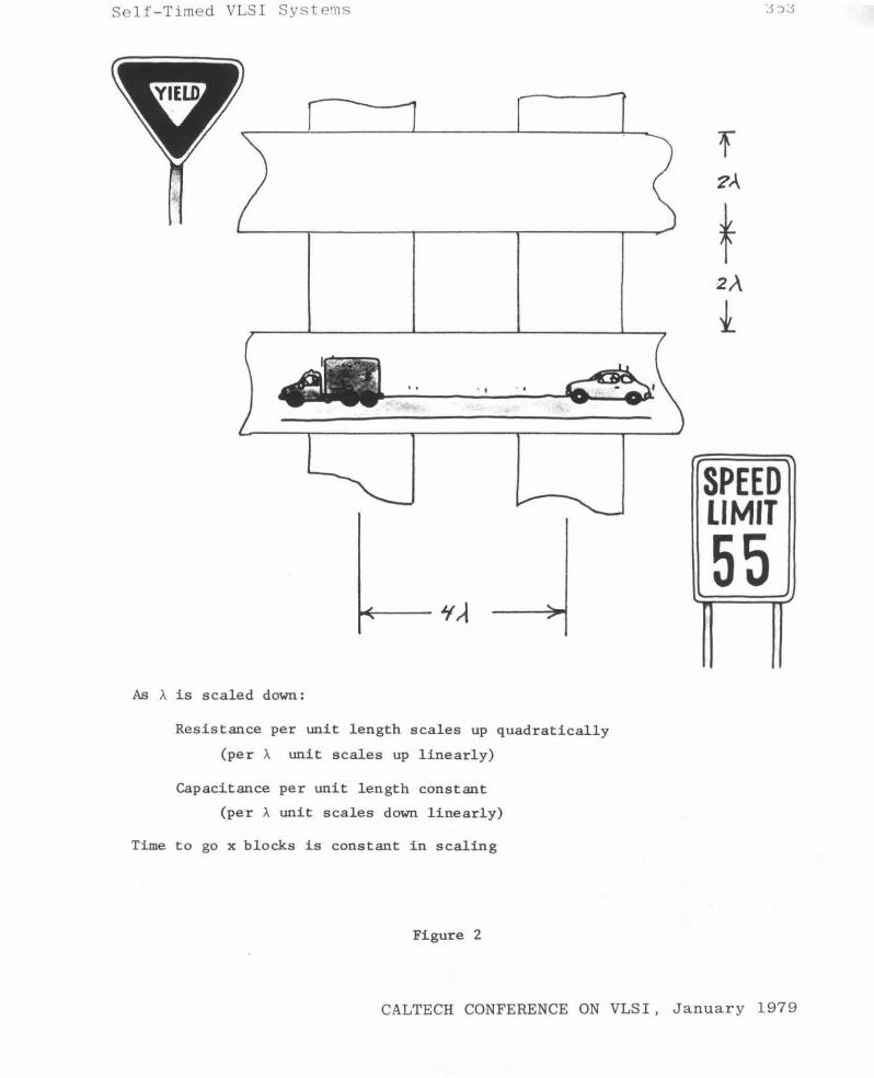
In Swrrma.ry , an Analogy
Let me share with you a simple analogy, illustrated in figures 2 and 3, and whose object is to provide another way of looking at the complexity and communication limitations the designer of VLSI systems will encounter. If one takes half of the width of a poly conductor as the length unit A (the same A as appears in Mead and Conway [1]), with the scaling of feature size
SELF-TIMED LOGIC SESSION
Self-Timed VLS I SystP~S
. I
As A is scaled down:
Resistance per unit length scales up quadratically
(per A unit scales up linearly)
Capacitance per unit length constant
(per A unit scales down linearly)
Time to go x blocks is constant in scaling
Figure 2
SPEED LIMIT
55
CALTECH CONFERENCE ON VLSI, January 1979

cnar~es L. ~e i L~
represented by changing the value of A, it turns out that the diffusion delay for a distance measured in A units is constant. A picture of this world looks not unlike a road network, so we note that the time required to communicate across a certain number of blocks remains constant as A is scaled.
Figure 3 shows four different stages of the microcircuit technology, with the result of making features smaller and chip areas larger by scaling up the chips to make their blocks similar to city blocks. The complexity of one of today's microprocessors is not unlike a multi-level road network covering the Los Angeles basin at urban density, e.g. not unlike L.A. really is. The next two stages illustrate not only the complexity, but also the communication problem that the time required to cross a chip increases even as the switches become faster. Local autonomy in function and in timing may work on VLSI chips just as it appears necessary in our social and political organization.
Referenoes
[1] Carver Mead and Lynn Conway, Introduction to VLSI Systems, Addison-Wesley, 1979.
[2] Amr Mohsen, "Devices and Circuits for VLSI", this issue.
[ 3] Ivan Sutherland and Carver Mead, "Microelectt::onics and Computer Science," Scientific American, September 1977.
SELF-TIMED LOGIC SESSION

Self-Timed VLSI Systems
c: l,63 [
sc~\~ fc.~\-v,. ~o ~c.c~e lo\oc.ks ~oo ~ "'rc..,.t:. c. ~ /r. ..... D~ rJ toode.)
~ t(r-\MW\
'2A 2 %.~
~A~ s-~
G I ~1&
~A=~ 2oM.. '~-
f./A~ I~
z '"~~ ? ~A'= ~ lOOM )C.
~A~2,r
"2 ~~~"?
2A-: 0.2 ~ a.too M y.
~A s ~.~
a
D
/0 "'"<
Figure 3
,-- ---- ., I
, ___ ---- --
CALTECH CONFERENCE ON VLSI, January 1979