Embed Size (px)
Citation preview
BECOME A SLOAN AFFILIATE http://www.sloan.org/programs/affiliates.shtml
SEMICONDUCTOR CAPABILITIES IN THE U.S.
AND INDUSTRIALIZING ASIA
Clair Brown and Greg Linden
University of California, Berkeley
2521 Channing Way #5555Berkeley, CA 94720-5555
Phone: (510) 643-8140 Fax: (510) 642-6432 www.irle.berkeley.edu
University of California, Berkeley
IRLE
Center for WORK,TECHNOLOGYand SOCIETY
SEMICONDUCTOR CAPABILITIESIN THE U.S. ANDINDUSTRIALIZING ASIA
Clair Brown and Greg LindenUniversity of California, BerkeleyMarch 2008
INSTITUTE FOR TECHNOLOGY,ENTERPRISE AND COMPETITIVENESS
Working Paper Series
1
Semiconductor Capabilities in the U.S. and Industrializing Asia1
Clair Brown and Greg Linden University of California, Berkeley
March 2008 The semiconductor industry has a rich experience with the offshoring of manufacturing activity. Semiconductor (or chip) companies were among the first to invest in offshore facilities to manufacture goods for import back to the U.S.
Because meaningful data about the extent of the offshoring are limited, we rely on a more qualitative analysis for our key points. We have conducted dozens of interviews with engineers and managers at numerous semiconductor and related companies in the United States, Asia, and Europe over the past twelve years. Our research also incorporates the rich store of publicly-available information in trade journals and company reports. The paper begins in section one with a brief description of the stages of semiconductor production and our analytical framework. Section two summarizes the offshoring of activities by the industry. Section three provides a more detailed discussion of the offshoring of design. Section four compares engineer capabilities in the relevant countries of Asia, where most offshoring occurs. Section five profiles the chip industry in Taiwan, China, and India. And Section six concludes with an outlook for the chip industry in the investing and host countries. 1. Introduction: The Semiconductor Industry In order to understand the offshoring of activities in the semiconductor industry, we begin by describing the stages of production. The most important type of semiconductor, and the one on which this study is focused, is the integrated circuit, or “chip,” which is basically a network of tiny wires fabricated on a surface connecting transistors that switch on and off for processing data in binary code.2 The development and manufacturing of chips involve three primary activities in the value chain: design, fabrication, test and assembly. The semiconductor industry has successively undergone the offshoring of each of these activities—first assembly, then fabrication, and now design.
1 This paper is based upon material from our forthcoming book Change is the Only Constant. The authors would like to thank the Alfred P. Sloan Foundation, the Institute for Research on Labor and Employment at UC Berkeley, and the Institute for Technology, Enterprise and Competitiveness (ITEC/COE) at Doshisha University, Japan, for funding. We are grateful to Ben Campbell, Bob Doering, David Ferrell, Michael Flynn, Gartner Dataquest, Ron Hira, Dave Hodges, Rob Leachman, Daya Nadamuni, Elena Obukhova, Devadas Pillai, Semiconductor Industry Association, Chintay Shih, Gary Smith, Bill Spencer, Strategic Marketing Associates, Yea-Huey Su, Tim Tredwell, and C-K Wang for their valuable contributions. Melissa Appleyard, Hank Chesbrough, Jason Dedrick, Rafiq Dossani, Richard Freeman, Deepak Gupta, Bradford Jensen, Ken Kraemer, Frank Levy, B. Lindsay Lowell, Jeff Macher, Dave Mowery, Tom Murtha, Tim Sturgeon, Michael Teitelbaum, and Eiichi Yamaguchi, as well as participants at the NAE Workshop on the Offshoring of Engineering, the 2005 Brookings Trade Forum on Offshoring of White-Collar Work, the Berkeley Innovation Seminar, and the Doshisha ITEC seminar series provided thoughtful discussions that improved the paper. 2 Other types of semiconductors, such as single transistors or diodes, use different design and manufacturing methods not subject to the same economic forces discussed in this paper. These other categories constituted about 15% of the total semiconductor market in 2004 (“WSTS Semiconductor Market Forecast,” World Semiconductor Trade Statistics press release dated November 2, 2004.).
2
During design, the desired electronic circuits progress through a series of abstract representations of increasing detail. During fabrication, the circuits of the chips are built up on the surface of a flat, round silicon wafer in successive layers Assembly is, typically, the process of cutting the wafer into individual chips (or die), which can number in the thousands, depending on die size, and packaging the delicate chip in a protective shell that includes connections to other components. The economic characteristics of each step of the process differ significantly. Design is skill intensive, and requires expensive EDA (electronic design automation) software, which is typically licensed per design engineer. Fabrication requires a huge fixed investment (currently on the order of $2 billion) to build a plant (called a fab) that holds a wide variety of expensive equipment and that meets extreme requirements of cleanliness. Assembly also requires expensive equipment, but the overall costs of plant and equipment are much lower than for the fab, as are the average skill requirements. Overall, worker skill requirements go down along the value chain (i.e., design is more skill-intensive than manufacturing, which is more skill-intensive than assembly). However, equipment costs dominate labor costs, especially for fabrication, and this has limited the attractiveness of low-cost labor locations. Even the most labor-intensive activity, chip assembly, has become more automated over time. As discussed below, other costs, including those relating to land, taxes, and government regulations, often affect decisions to invest offshore. In the longer term, numerous firm-level investments in a foreign location may transform the location in such a way that it presents a new set of opportunities that lead to a transformation of the industry. A foreign location that is initially little more than a source of lower costs, especially labor, might develop over time as a specialized supply base, particularly in the presence of incentives and infrastructure provided by the host country government. The changes can increase the value of the location to the point that the industry eventually restructures around the new distribution of skills such that offshoring becomes the preferred mode for this part of the value chain. It will be discussed below how this occurred for semiconductor assembly, but it has also taken place in other industries, such as hard disk drives.3 In other words, the pursuit of offshoring to gain competitive advantage in the context of a growing market initiates a dynamic process that has implications for both host and investing countries.
U.S. companies and analysts have been raising the warning flags about the potential loss of industry leadership to newcomers, Taiwan, China and India. We have come full circle back to the Japan crisis of the 1980s in a new guise—fear of loss of competitive advantage to Asian rivals. In this paper we analyze the global realignment of the industry as greater China and India have become key players in the industry both as suppliers and as consumers. We begin by looking at the movement of manufacturing and design activities abroad by U.S. companies. Then we look in detail at the current state of the semiconductor industry in Taiwan, China and India, where the industry has been developing rapidly, and compare the industry capabilities in those countries to the two industry leaders, United States and Japan.
The current fear of loss of industry leadership is based on the continual escalation of fabrication and design costs combined with competition for the global labor supply of 3 McKendrick, Doner, and Haggard (2000).
3
engineers, which may provide the fast-growing and lower-cost nations of China and India a chance to catch up, and pass, the U.S., especially as Asian markets provide a large part of the growth in global chip demand. Observers also fear loss of U.S. leadership in innovation, since private firms, faced with the low return and high risk on investment and the looming technological challenges to staying on Moore’s law, have become less willing and able to shoulder the continual need for large R&D expenditures.
One version of the current crisis is predicted loss of U.S. industry leadership as a result of R&D following manufacturing to China. We consider this a simplified variant of the current crisis. The fear that the U.S. will become less innovative and no longer be the leader in developing new technologies is based upon the assumption that research and development in leading-edge technology follows manufacturing abroad. In the semiconductor industry, we have not observed this occurring as foundries, especially in Taiwan, have taken over a growing proportion of chip manufacturing. As we discuss below, foundries provide leading-edge process technology, often in alliance with U.S. industry leaders, as well as design services for customers. These activities have served as a complement to innovation activities for U.S. fabless startups as well as mature chip companies, which have been relying increasingly on contract fabrication abroad.
2. Sending activities abroad
The three primary reasons for locating value chain activities globally are 1)access to location-specific resources, especially engineering talent; 2) cost reduction; and 3) local market development and access. Often, the shift of an activity to a new location via internal investment or outsourcing is in response to all three reasons. For example, a company may move chip design to China in order to take advantage of engineering talent that is low cost and knowledgeable about customized solutions for the regional Chinese telecommunication systems as well as to gain government approval for market access.
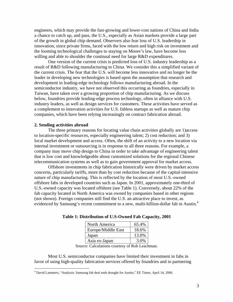
Offshore investments in chip fabrication historically were driven by market access concerns, particularly tariffs, more than by cost reduction because of the capital-intensive nature of chip manufacturing. This is reflected by the location of most U.S.-owned offshore fabs in developed countries such as Japan. In 2001, approximately one-third of U.S.-owned capacity was located offshore (see Table 1). Conversely, about 22% of the fab capacity located in North America was owned by companies based in other regions (not shown). Foreign companies still find the U.S. an attractive place to invest, as evidenced by Samsung’s recent commitment to a new, multi-billion-dollar fab in Austin.4
Table 1: Distribution of U.S-Owned Fab Capacity, 2001
North America 65.4%Europe/Middle East 18.6%Japan 13.0%Asia ex-Japan 3.0%
Source: Calculations courtesy of Rob Leachman.
Most U.S. semiconductor companies have limited their investment in fabs in favor of using high-quality fabrication services offered by foundries and in partnering 4 David Lammers, “Analysis: Samsung fab deal ends drought for Austin,” EE Times, April 14, 2006.
4
with them to develop next generation fabrication processes. For example, TI announced that the company would no longer develop process technology in-house beginning with 0.32-micron generation. Instead TI would partner with TSMC and UMC to develop process technology for contract fabrication. In 2005, the outsourced fabrication market was worth $18 billion,5 with most of it accounted for by the foundries in Taiwan. The first foundry, Taiwan Semiconductor Manufacturing Corporation (TSMC), remains the largest. If it sold chips under its own name, TSMC would have made the chip industry’s top 10 list in 2005 with $8.2 billion in revenue, although foundries are excluded to avoid double-counting of their and their customers’ chips. Since foundry price is about one-third of the final chip value, TSMC actually manufactured nearly $25 billion worth of chips, which would place it number two in the overall chip industry behind only Intel.
Specialized skills are an important reason that U.S. semiconductor companies invest overseas, particularly in Europe. Britain, for example, has developed expertise in consumer multimedia, and Scandinavian countries are noted for their skills in wireless network technology. U.S. firms regularly acquire small European companies to obtain both application know-how and a team of pre-trained engineers.
As is true of fabrication, design offshoring works both ways, and many foreign companies maintain a Silicon Valley or other U.S. design center to take advantage of the high skills and productivity available there as well as to be closer to U.S. customers. Philips of the Netherlands, for example, bought VLSI Technology, a major ASIC company with over 2,000 employees (about one-third of whom were fab workers), in 1999 for nearly $1 billion.6 Hitachi Semiconductor has a U.S. design group several hundred strong.7 Toshiba has a network of seven ASIC design centers around the United States.8 Even foreign start-ups may need to have a U.S. design team to work with U.S. customers or to access leading-edge analog design skills.
However the reason for design offshoring that is perhaps getting the most attention is cost reduction. For Silicon Valley firms, some cost reduction is available by opening satellite design centers elsewhere in the U.S., where some locations have average engineering salaries that are up to 20% lower than those in the Silicon Valley. But these salaries are still much higher than salaries in India and elsewhere, as discussed below.
Cost-driven in-house offshoring incurs non-wage costs that partially offset the difference in salaries, especially during the early stages of establishing an offshore design center. One that is often mentioned is the lower quality and productivity of inexperienced engineers, which also adds monitoring costs. The time and inconvenience of communicating across time zones can also be considerable. Additional control mechanisms may also be needed to protect key intellectual property. According to a venture capitalist, the actual savings from going offshore is more likely to be 25 to 50% rather than the 80 to 90% suggested by a simple salary comparison.9
U.S. chip firms have opened an increasing number of low-cost design subsidiaries in Asia, especially India, over the last decade. Among the top twenty U.S. semiconductor
5 Gartner Dataquest estimate reported in “Foundry Revenue Drops in 2005, Gartner Reports,” Electronic News, March 27, 2006. 6 “Philips to acquire VLSI Technology for $953 million,” Semiconductor Business News, May 3, 1999. 7 “Hitachi Forms North America Semiconductor Systems Solutions Unit,” Hitachi Press Release, September 2, 1998. 8 “Toshiba Expands Soc Design Support Network With Opening Of San Diego Design Center,” Toshiba Press Release, November 26, 2002. 9 Interview, May 2004.
5
companies, only two have not established a design center in India. This movement to establish design centers in India is quite recent, and for most companies is in a very early stage. Nine of these companies opened their Indian operations since 2004. The size of the operations varies widely, from about several thousand engineers at Intel and TI to fewer than 100 at smaller companies.
The growing importance of China and India as providers of various activities in the supply chain, especially manufacturing for China and design for India, and as the fastest expanding markets for cell phones and computers, may threaten US market leadership in the long run. Here we look at the recent past and ask to what extent have U.S. chip companies moved their engineering jobs abroad over the past decade.
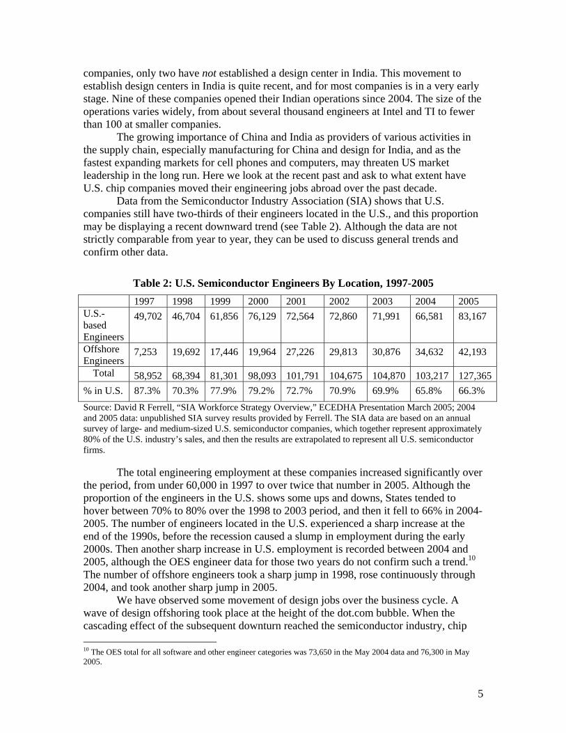
Data from the Semiconductor Industry Association (SIA) shows that U.S. companies still have two-thirds of their engineers located in the U.S., and this proportion may be displaying a recent downward trend (see Table 2). Although the data are not strictly comparable from year to year, they can be used to discuss general trends and confirm other data.
Table 2: U.S. Semiconductor Engineers By Location, 1997-2005 1997 1998 1999 2000 2001 2002 2003 2004 2005 U.S.-based Engineers
49,702 46,704 61,856 76,129 72,564 72,860 71,991 66,581 83,167
Offshore Engineers
7,253 19,692 17,446 19,964 27,226 29,813 30,876 34,632 42,193
Total 58,952 68,394 81,301 98,093 101,791 104,675 104,870 103,217 127,365% in U.S. 87.3% 70.3% 77.9% 79.2% 72.7% 70.9% 69.9% 65.8% 66.3% Source: David R Ferrell, “SIA Workforce Strategy Overview,” ECEDHA Presentation March 2005; 2004 and 2005 data: unpublished SIA survey results provided by Ferrell. The SIA data are based on an annual survey of large- and medium-sized U.S. semiconductor companies, which together represent approximately 80% of the U.S. industry’s sales, and then the results are extrapolated to represent all U.S. semiconductor firms.
The total engineering employment at these companies increased significantly over the period, from under 60,000 in 1997 to over twice that number in 2005. Although the proportion of the engineers in the U.S. shows some ups and downs, States tended to hover between 70% to 80% over the 1998 to 2003 period, and then it fell to 66% in 2004-2005. The number of engineers located in the U.S. experienced a sharp increase at the end of the 1990s, before the recession caused a slump in employment during the early 2000s. Then another sharp increase in U.S. employment is recorded between 2004 and 2005, although the OES engineer data for those two years do not confirm such a trend.10 The number of offshore engineers took a sharp jump in 1998, rose continuously through 2004, and took another sharp jump in 2005.
We have observed some movement of design jobs over the business cycle. A wave of design offshoring took place at the height of the dot.com bubble. When the cascading effect of the subsequent downturn reached the semiconductor industry, chip 10 The OES total for all software and other engineer categories was 73,650 in the May 2004 data and 76,300 in May 2005.
6
companies cut staff at home. Now that the recovery requires expansion of design operations, chip companies appear to be expanding design operations abroad faster than at home.11 It is too early to predict where this relative shift in the geographic distribution of employment will find a new equilibrium.
3. Relocating Design Activities to Lower Costs
We now take a closer look at the offshoring of chip design to reduce costs. All parts of chip design and development, from specification to finished chips, can be done by different teams, either in-house or outsourced, and either locally or offshore. Locational decisions of chip design are based on three primary factors related to competitive advantage: closer contact with customers, access to specialized skilled labor, and cost reduction. Here we focus on cost reduction, although the other two factors play a role that may or may not overlap with lower costs (Brown and Linden, 2005).
The easiest part of chip design to offshore or outsource is physical design because it is a relatively standardized task. It is also the least sensitive part of design in terms of revealing the customer’s intellectual property. However for designs requiring leading-edge process technology such as 90nm linewidths, layout has become much less straightforward because of the sensitivity of the atomic-scale wiring. In such a case, physical design is likely to be outsourced only by small and medium companies that lack the resources to develop the necessary expertise in-house. On the other hand, we interviewed one (well-funded) start-up whose initial design was so complex that outsourcing any parts wasn’t an option.12
Another design function that is frequently offshored or outsourced is logic verification, the resource-intensive task of making sure that that first stages of the physical implementation are a correct translation of the abstract logic. At the other extreme, architectural design, or the design of key functional blocks containing proprietary algorithms are the least likely to be outsourced because of the risk of exposing proprietary knowledge.13
First let us look at moving in-house design activities to areas with lower salaries, and then turn to outsourcing activities, both at home and abroad.
For Silicon Valley firms, some cost reduction is available by opening satellite design centers elsewhere in the U.S., where some locations have average engineering salaries that are up to 20% lower than salaries in the Silicon Valley. But these salaries are still much higher than salaries in India and elsewhere.14 The prospects for cost reduction offshore have become much more feasible with the availability of the global high-bandwidth infrastructure and the economic liberalization of large economic areas in Eastern Europe, and especially Asia.15 Dividing chip designs across locations presents a number of managerial challenges. The sacrifice of face-to-face interaction between different parts of the design team can adversely affect productivity, and distance makes it harder to evaluate and reward individual contributions to team performance. Task assignments must be more
11 See, for example, “The perfect storm brews offshore,” Electronic Business, March 2004, accessible at www.reed-electronics.com/eb-mag/toc/03%2D01%2D2004/ 12. Interview, November 2004. 13. “Outsourcing trend proves: Complex by design,” EE Times, January 31, 2005, and interview, April 2004. 14. “Mean wages edge closer to six-figure mark,” EE Times, August 25, 2004. 15. Ernst (2004).
7
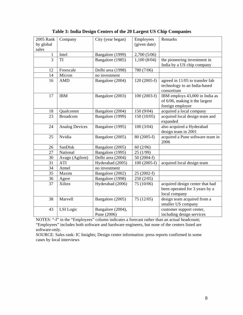
carefully codified for offshore teams than for locally-based engineers, and managers will need to travel periodically between locations. When the separation is across borders, there are also cultural differences that can make communication less effective. A high-level manager at a design center of a U.S. multinational in Bangalore told us about communication problems between teams in India and the U.S., especially when projects were initially being developed. A major cultural difference was the Indian engineers’ reluctance to disagree with their superiors or to speak up with suggestions for improvements since this might appear to be critical of others. Indian engineers would agree to proposed timelines even when they could not be met, since saying that the time was too short indicated the engineers were not up to the task.16 Cost-driven in-house offshoring incurs other costs that partially offset the difference in salaries, especially during the early stages of establishing an offshore design center. One that is often mentioned, and one observed in our fieldwork, is the lower quality and productivity of inexperienced engineers. This raises monitoring costs, and offshore engineers may also require a longer training period than a U.S. team would need. Additional controls may also be needed to protect key intellectual property. According to a venture capitalist, the actual savings from going offshore is more likely to be 25 to 50% rather than the 80 to 90% suggested by a simple salary comparison.17 Design offshoring can run up against national security barriers. For example, the U.S. government has placed limits on the export of advanced encryption technology. Communications chips that employ such technology are difficult to design offshore. Either the chip design must be compartmentalized, with the encryption block designed only in the United States, or government approval, subject to possible delays, must be obtained in advance.18 Yet despite these pitfalls, the amount of offshore design in industrializing economies has noticeably expanded in recent years, especially in India (Bangalore in particular). Among the top twenty U.S. semiconductor companies, only two have not established a design center in India (see Table 3). Nine of these companies opened their Indian operations since 2004, and so their operations are in a very early stage. The company with the most mature Indian design operations is Texas Instruments, which in 1985 was the first U.S. company to establish design operations in India. In the mid- to late-1990s, six U.S. companies, including Intel, Motorola (now Freescale), and Broadcom, set up Indian design centers. The size of the operations varies widely, with Intel employing 2,700 engineers (2006) to Maxim potentially hiring 25 engineers (2002). The training curve for domestically-educated engineers can be steep. In one instance we studied, a chip design project took twice as long to complete as planned.19 The range of activities is quite broad, and can include simple parts of the design flow of a mature technology or can include the entire design flow as at TI.
16. Interview, November 2005. 17. Interview, May 2004. 18. Interview, December 2004. 19. E-mail communications with Indian chip designer, June 2005.
8
Table 3: India Design Centers of the 20 Largest US Chip Companies 2005 Rank by global sales
Company City (year began) Employees (given date)
Remarks
1 Intel Bangalore (1999) 2,700 (5/06) 3 TI Bangalore (1985) 1,100 (8/04) the pioneering investment in
India by a US chip company 12 Freescale Delhi area (1998) 780 (7/06) 14 Micron no investment 16 AMD Bangalore (2004) 120 (2005-f) agreed in 11/05 to transfer fab
technology to an India-based consortium
17 IBM Bangalore (2003) 100 (2003-f) IBM employs 43,000 in India as of 6/06, making it the largest foreign employer
18 Qualcomm Bangalore (2004) 150 (9/04) acquired a local company 23 Broadcom Bangalore (1999) 150 (10/05) acquired local design team and
expanded 24 Analog Devices Bangalore (1995) 100 (3/04) also acquired a Hyderabad
design team in 2001 25 Nvidia Bangalore (2005) 80 (2005-f) acquired a Pune software team in
2006 26 SanDisk Bangalore (2005) 60 (2/06) 27 National Bangalore (1995) 25 (1/99) 30 Avago (Agilent) Delhi area (2004) 50 (2004-f) 31 ATI Hyderabad (2005) 100 (2005-f) acquired local design team 34 Atmel no investment 35 Maxim Bangalore (2002) 25 (2002-f) 36 Agere Bangalore (1998) 250 (2/05) 37 Xilinx Hyderabad (2006) 75 (10/06) acquired design center that had
been operated for 3 years by a local company
38 Marvell Bangalore (2005) 75 (12/05) design team acquired from a smaller US company
43 LSI Logic Bangalore (2004), Pune (2006)
customer support center, including design services
NOTES: “-f” in the “Employees” column indicates a forecast rather than an actual headcount; “Employees” includes both software and hardware engineers, but none of the centers listed are software-only. SOURCE: Sales rank: IC Insights; Design center information: press reports confirmed in some cases by local interviews
9
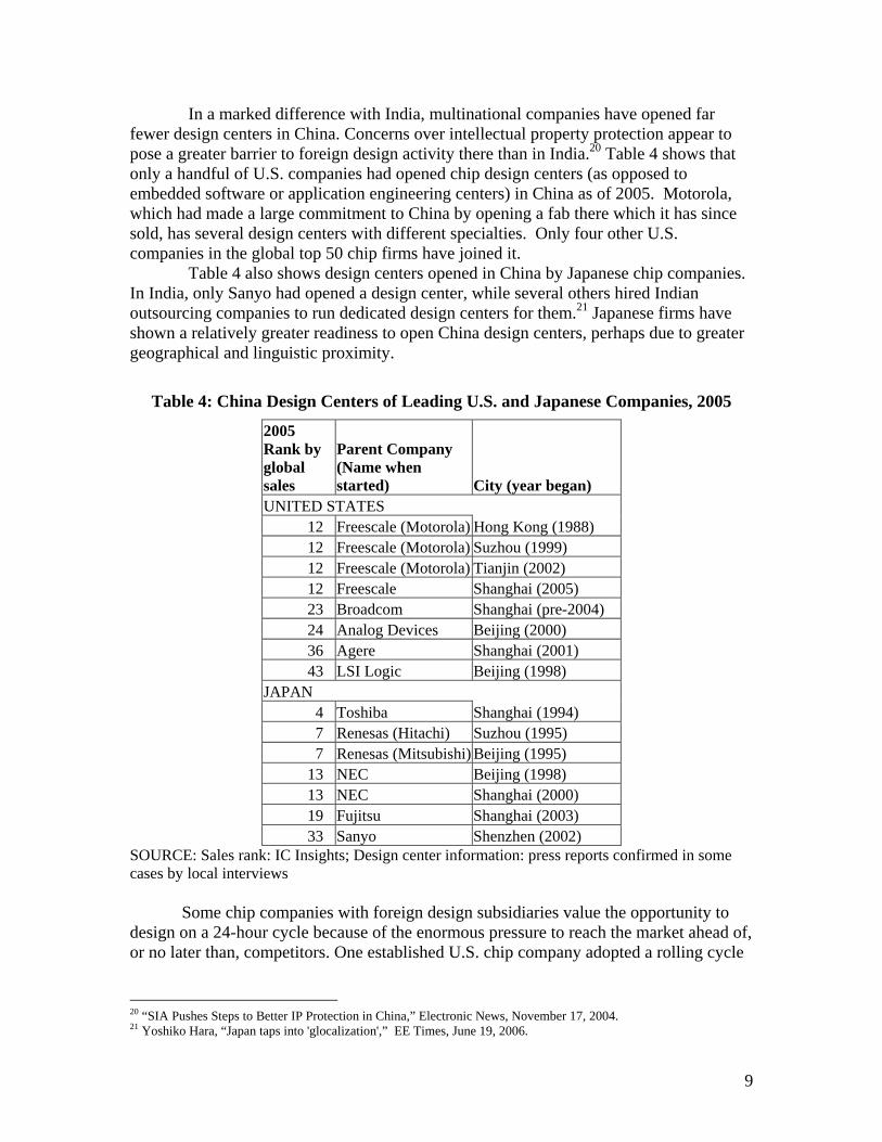
In a marked difference with India, multinational companies have opened far fewer design centers in China. Concerns over intellectual property protection appear to pose a greater barrier to foreign design activity there than in India.20 Table 4 shows that only a handful of U.S. companies had opened chip design centers (as opposed to embedded software or application engineering centers) in China as of 2005. Motorola, which had made a large commitment to China by opening a fab there which it has since sold, has several design centers with different specialties. Only four other U.S. companies in the global top 50 chip firms have joined it.
Table 4 also shows design centers opened in China by Japanese chip companies. In India, only Sanyo had opened a design center, while several others hired Indian outsourcing companies to run dedicated design centers for them.21 Japanese firms have shown a relatively greater readiness to open China design centers, perhaps due to greater geographical and linguistic proximity.
Table 4: China Design Centers of Leading U.S. and Japanese Companies, 2005
2005 Rank by global sales
Parent Company (Name when started) City (year began)
UNITED STATES 12 Freescale (Motorola) Hong Kong (1988) 12 Freescale (Motorola) Suzhou (1999) 12 Freescale (Motorola) Tianjin (2002) 12 Freescale Shanghai (2005) 23 Broadcom Shanghai (pre-2004) 24 Analog Devices Beijing (2000) 36 Agere Shanghai (2001) 43 LSI Logic Beijing (1998)
JAPAN 4 Toshiba Shanghai (1994) 7 Renesas (Hitachi) Suzhou (1995) 7 Renesas (Mitsubishi) Beijing (1995)
13 NEC Beijing (1998) 13 NEC Shanghai (2000) 19 Fujitsu Shanghai (2003) 33 Sanyo Shenzhen (2002)
SOURCE: Sales rank: IC Insights; Design center information: press reports confirmed in some cases by local interviews
Some chip companies with foreign design subsidiaries value the opportunity to design on a 24-hour cycle because of the enormous pressure to reach the market ahead of, or no later than, competitors. One established U.S. chip company adopted a rolling cycle
20 “SIA Pushes Steps to Better IP Protection in China,” Electronic News, November 17, 2004. 21 Yoshiko Hara, “Japan taps into 'glocalization',” EE Times, June 19, 2006.
10
between design centers in the United States, Europe, and India.22 More common is the bi-national arrangement used by a Silicon Valley start-up that had all of its design beyond the initial specification done by a China subsidiary established only months after the head office was set up. Ten executives in the head office had to train the mostly inexperienced staff in Beijing, which was about thirty strong.23 The Silicon Valley staff would review Beijing’s work from the previous day then spend up to three hours on the phone (starting around 5pm California time) providing feedback and reviewing assignments for that day in Beijing. In a single-location firm, this work-feedback cycle would take two days. Venture capitalists have reportedly begun to require start-ups to include some offshoring in their business plans in order to better leverage their resources. A typical comment is, “We don't fund chip designs that don't outsource to India. If you rely on Indian contractors for the things they do well, you can get a chip out for under $10 million. If you don't, you can't, and you won't be competitive. It's that simple.”24 PortalPlayer, the company behind the key multimedia chip in Apple’s iPod, is a recent example of a successful start-up that set up an Indian software and chip design subsidiary within a few months of its founding in 1999.25 Low-cost design engineering resources can also be tapped through international outsourcing, although to date most design outsourcing by U.S. companies takes place domestically. Many interviewees reported that they outsource physical design to small local companies on an as-needed basis. The leading suppliers of design services worldwide are the leading design automation software vendors, Cadence Design Systems, Synopsys, and Mentor Graphics. Their annual services revenue is about $300 million out of a total outsourced design market estimated at $2.5 billion.26 As this suggests, the remaining market is highly fragmented.
The availability of outsourcing (foreign or domestic) is particularly important for small companies and start-ups because of the relatively large fixed cost of EDA tools, which are typically licensed per engineer. One consultant estimated that the minimum annual software expense for a small company is $10 million.27 For the industry as a whole, EDA expense runs close to 1% of revenue. In that case, a company earning less than $1 billion in revenue would be below the efficient scale for in-house design. Only the nine largest fabless companies met that criterion in 2004. One consultant estimated that outsourcing even within the United States would save a small start-up that does fewer than five designs a year up to two-thirds the cost of doing the work in-house.28 Another type of customer for outsourced design services are the systems companies, such as Apple Computer or Cisco. Although these companies often design chips in-house either to protect intellectual property or to reduce the cost of custom chips, they may turn to outside (and possibly offshore) service providers for part of the design process.
22. Interview, April 1998. 23. Interview, August 2004. 24. William Quigley, managing director at Clearstone Venture Partners (Menlo Park, Calif.), quoted in “Venture capitalist explains new rules for IC startups,” EE Times, January 16. 2003. 25. “Designs for Digital Audio, Auto Electronics,” Nikkei Electronics Asia, October 2002. 26. “Complex chips reignite demand for design services,” EE Times, October 11, 2004. 27. International Business Strategies (2002). 28. Interview, April 2004.
11
4. Engineer Capabilities across Countries
In order to assess the semiconductor capabilities of companies across countries, we look in more detail at the availability, quality (education and skills), and cost of chip engineers, which largely determines the technology capability of the companies.
A major problem with comparing semiconductor engineering talent across countries is that the engineers in China and India, and to a lesser extent Taiwan, are younger with less experience and less education than the engineers in the U.S. and Japan. In India and China, technicians with a two-year degree are often classified as engineers, and this is not usually the case in the U.S. and Japan. India and China have very little graduate training available in semiconductor engineering, and what is available is not comparable to the graduate programs in the U.S. and Japan. Taiwan is an intermediate case, where their undergraduate and masters engineering programs are comparable to those in the U.S. and Japan, although their PhD programs are still catching up.
Taiwan’s semiconductor industry was built in large part by PhD engineers who returned after receiving their degrees and valuable work experience in the United States. We see a similar process occurring in China and India, and in many ways we think that Taiwan provides us with a benchmark of how semiconductor engineering will develop in India and China as the semiconductor industry matures, with the important difference that Taiwan is a much smaller country. In India and China, the industry is still quite young in design, in which both countries are active, and in fabrication, which is not yet occurring in India. Subsidiaries of multinational companies (MNCs) are playing a major role in the development of the semiconductor industry in India. In China, domestic companies, often with personnel and funds from Taiwan and government subsidies, are playing a major role in semiconductor design. In China’s fabrication sector, both MNCs and domestic companies (again with government subsidies and labor and capital from Taiwan) are playing a major role in semiconductor fabrication in China.
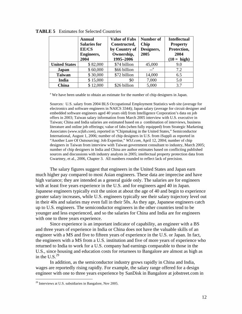
Overview of engineering in Asia. With the caveat that comparing semiconductor engineering talent in the U.S., Japan, Taiwan, China and India means comparing engineers with different education and experience, we present rough estimates for engineer salaries in Table 2, which is based on a combination of published sources and interviews.
We also include the value of fabs constructed, the number of active chip designers (excluding embedded software), and an index of intellectual property protection for these countries. IP protection is an important consideration in deciding what engineering activities to undertake in other countries.
12
TABLE 5 Estimates for Selected Countries Annual
Salaries for EE/CS Engineers, 2004
Value of Fabs Constructed, by Country of
Ownership, 1995–2006
Number of Chip Designers, 2005
Intellectual Property
Protection, 2004
(10 = high) United States $ 82,000 $74 billion 45,000 9.0
Japan $ 60,000 $66 billion --a 7.2 Taiwan $ 30,000 $72 billion 14,000 6.5 India $ 15,000 $0 7,000 5.0 China $ 12,000 $26 billion 5,000 3.7
a We have been unable to obtain an estimate for the number of chip designers in Japan. Sources: U.S. salary from 2004 BLS Occupational Employment Statistics web site (average for electronics and software engineers in NAICS 3344); Japan salary (average for circuit designer and embedded software engineers aged 40 years old) from Intelligence Corporation’s data on job offers in 2003; Taiwan salary information from March 2005 interview with U.S. executive in Taiwan; China and India salaries are estimated based on a combination of interviews, business literature and online job offerings; value of fabs (when fully equipped) from Strategic Marketing Associates (www.scfab.com), reported in “Chipmaking in the United States,” Semiconductor International, August 1, 2006; number of chip designers in U.S. from iSuppli as reported in “Another Lure Of Outsourcing: Job Expertise,” WSJ.com, April 12, 2004; number of chip designers in Taiwan from interview with Taiwan government consultant to industry, March 2005; number of chip designers in India and China are author estimates based on conflicting published sources and discussions with industry analysts in 2005; intellectual property protection data from Gwartney, et al., 2006, Chapter 3. All numbers rounded to reflect lack of precision.
The salary figures suggest that engineers in the United States and Japan earn
much higher pay compared to most Asian engineers. These data are imprecise and have high variance; they are intended as a general guide only. The salaries are for engineers with at least five years experience in the U.S. and for engineers aged 40 in Japan. Japanese engineers typically exit the union at about the age of 40 and begin to experience greater salary increases, while U.S. engineers typically see their salary trajectory level out in their 40s and salaries may even fall in their 50s. As they age, Japanese engineers catch up to U.S. engineers. The semiconductor engineers in the other countries tend to be younger and less experienced, and so the salaries for China and India are for engineers with one to three years experience.
Since experience is an important indicator of capability, an engineer with a BS and three years of experience in India or China does not have the valuable skills of an engineer with a MS and five to fifteen years of experience in the U.S. or Japan. In fact, the engineers with a MS from a U.S. institution and five of more years of experience who returned to India to work for a U.S. company had earnings comparable to those in the U.S., since housing and education costs for returnees to Bangalore are almost as high as in the U.S.29
In addition, as the semiconductor industry grows rapidly in China and India, wages are reportedly rising rapidly. For example, the salary range offered for a design engineer with one to three years experience by SanDisk in Bangalore at jobstreet.com in 29 Interviews at U.S. subsidiaries in Bangalore, Nov 2005.
13
June 2005 was $9,200 to $18,400 .30 In our interviews at semiconductor design firms in India, we were repeatedly told that earnings of domestically-trained Indian engineers have been doubling in their first five years on the job. Senior managers with foreign experience are paid a large premium that mostly wipes out any cost advantage, since these managers are critical in implementing new technology and projects and the housing and education costs in Bangalore are almost as high as in U.S. cities.31
The value of fab construction over the past decade gives some idea of the presence of this part of the value chain in each country. China, at $26 billion, has made significant inroads since its early public-private joint ventures with Japan’s NEC in the mid-1990s. India, in sharp contrast, has yet to see a single commercial-scale fab constructed, although several have been proposed.
We also estimated the number of chip designers, since this group is critical to developing the semiconductor industry. However the number of chip designers can be misleading, since there is confusion about the definition of “chip designer”. Some sources put the number of chip designers being added each year in India and China on the order of 400 each.32 One industry executive claimed that the number of “qualified IC designers” in China in 2004 was only 500.33 A Taiwan consultant didn’t even consider the later (and lower-skilled) stage of physical design, called “place and route,” to be part of chip design;34 this group amounts to about 30% of the Taiwan designers shown in the table. Lastly, the IP protection rating shown covers all industries, and so weak scores in the table may be driven by lapses in specific sectors such as pharmaceuticals, trademark goods, or recorded media, which are not relevant to the semiconductor industry. Despite their lack of precision, these data indicate that the stock of Asian design engineers the emerging giant economies of China and India is growing quickly and represents an important source of supplemental engineering talent globally. The capability of engineers globally depends largely upon the quality of domestic higher education and the number of engineers sent to the U.S. (and elsewhere) for graduate training, which we discuss next. Comparison of higher education. The United States leads the world in higher education, and especially in graduate training, as the Academic Ranking of World Universities (http://ed.sjtu.edu.cn/ranking.htm) by Shanghai JiaoTong University shows (see Table 6). Fifty-three of the top one hundred universities are located in the U.S. and five are in Japan. In the top five hundred universities, 168 are in the U.S., 34 are in Japan, and only 21 are in China, Taiwan, and India combined. Graduate training in the U.S. is an important source of technology capability in Asia if foreign students return home. U.S. universities have attracted large numbers of foreign students to their engineering programs. In 2005, 63% of 6404 engineering PhDs were granted to noncitizen students, and 31% went to students from China (1422 PhDs),
30 converted at 43.52 Indian Rupees to the dollar 31 Interviews at fifteen semiconductor design centers in Bangalore in November 2005. 32 For India: “Designs on the future,” IT People, February 10, 2003; for China: “China’s Impact on the Semiconductor Industry,” PriceWaterhouseCoopers, December 2004, p.7. 33 “China’s Impact on the Semiconductor Industry,” PriceWaterhouseCoopers, December 2004, p.7. 34 E-mail exchange, March 2005.
14
Korea (525 PhDs), India (505 PhDs), and Taiwan (164 PhDs). Foreigners earned even more of the PhD degrees in Electrical Engineering (69%).35
Foreign-born U.S.-educated engineers can help develop the semiconductor industry in their home countries through two routes—returning to work in their home country or starting a new company in the United States with activities in the home country. Both of these paths are used by a small but influential number of engineers from India and China.36 Although the lifetime return rates for engineers is not known, at the time of graduation 80 to 85% of noncitizen PhD graduates planned on remaining in the U.S. to work.37 However only 60% of the noncitizen graduates, compared to 70% of citizen graduates, had made plans, and this indicates that perhaps many were having trouble acquiring a visa required to work in the U.S.
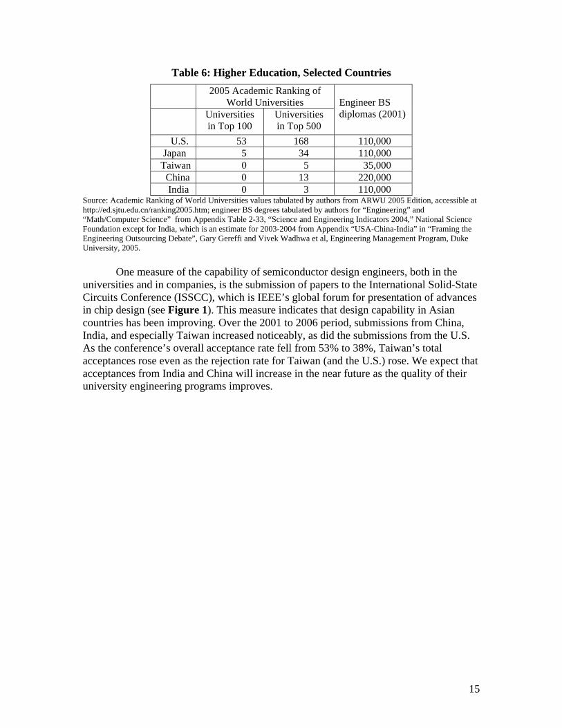
If we look at engineer BS graduation rates by country, we see that China and India produce many engineers with a BS degree, but that most of them graduate from low-ranked colleges (Table 6). The graduation numbers may indicate political and social commitment to advancing technical education rather than actual capability. Also, these numbers are dynamic because of continuing drives to expand engineering degree programs in India and especially China. According to a widely-cited Duke University study, the number of new EE-CS-IT bachelor degrees in China in 2004 had reached 350,000 (Gereffi and Wadhwa, 2005), but how long it will take the new programs to develop quality teaching programs is an open question.
Although China and India have large numbers of engineering graduates, the graduates from U.S. universities, according to our interviews, are better trained, especially in team work on projects and on tools and equipment. For example, undergraduate students in India and China usually do not have the opportunity to work on automated chip design (EDA) tools, while EE students in the U.S. do. According to McKinsey, only 10% of Chinese and 25% of Indian engineering graduates are likely to be suitable for employment by U.S. multinationals (McKinsey Global Institute, 2005).38
35 Data from National Science Foundation, Science and Engineering Doctorate Awards: 2005, accessed online at http://www.nsf.gov/statistics/nsf07305/content.cfm?pub_id=3757&id=2 Tables 3 and 11. 36 See Saxenian, AnnaLee, “International Mobility of Engineers and the Rise of Entrepreneurship in the Periphery”. WIDER Research Paper No. 2006/142, Nov 2006, which discusses the role of entrepreneurs from India and China, educated in the U.S., in the Silicon Valley. 37 Data from National Science Foundation, Science and Engineering Doctorate Awards: 2005, accessed online at http://www.nsf.gov/statistics/nsf07305/content.cfm?pub_id=3757&id=2 Table 13. 38 These figures were arrived at by McKinsey based on a survey of HR managers at multinational subsidiaries in these and other countries which asked the question: “Of 100 graduates with the correct degree, how many could you employ if you had demand for all?”
15
Table 6: Higher Education, Selected Countries 2005 Academic Ranking of
World Universities Universities
in Top 100 Universities in Top 500
Engineer BS diplomas (2001)
U.S. 53 168 110,000 Japan 5 34 110,000 Taiwan 0 5 35,000 China 0 13 220,000 India 0 3 110,000
Source: Academic Ranking of World Universities values tabulated by authors from ARWU 2005 Edition, accessible at http://ed.sjtu.edu.cn/ranking2005.htm; engineer BS degrees tabulated by authors for “Engineering” and “Math/Computer Science” from Appendix Table 2-33, “Science and Engineering Indicators 2004,” National Science Foundation except for India, which is an estimate for 2003-2004 from Appendix “USA-China-India” in “Framing the Engineering Outsourcing Debate”, Gary Gereffi and Vivek Wadhwa et al, Engineering Management Program, Duke University, 2005.
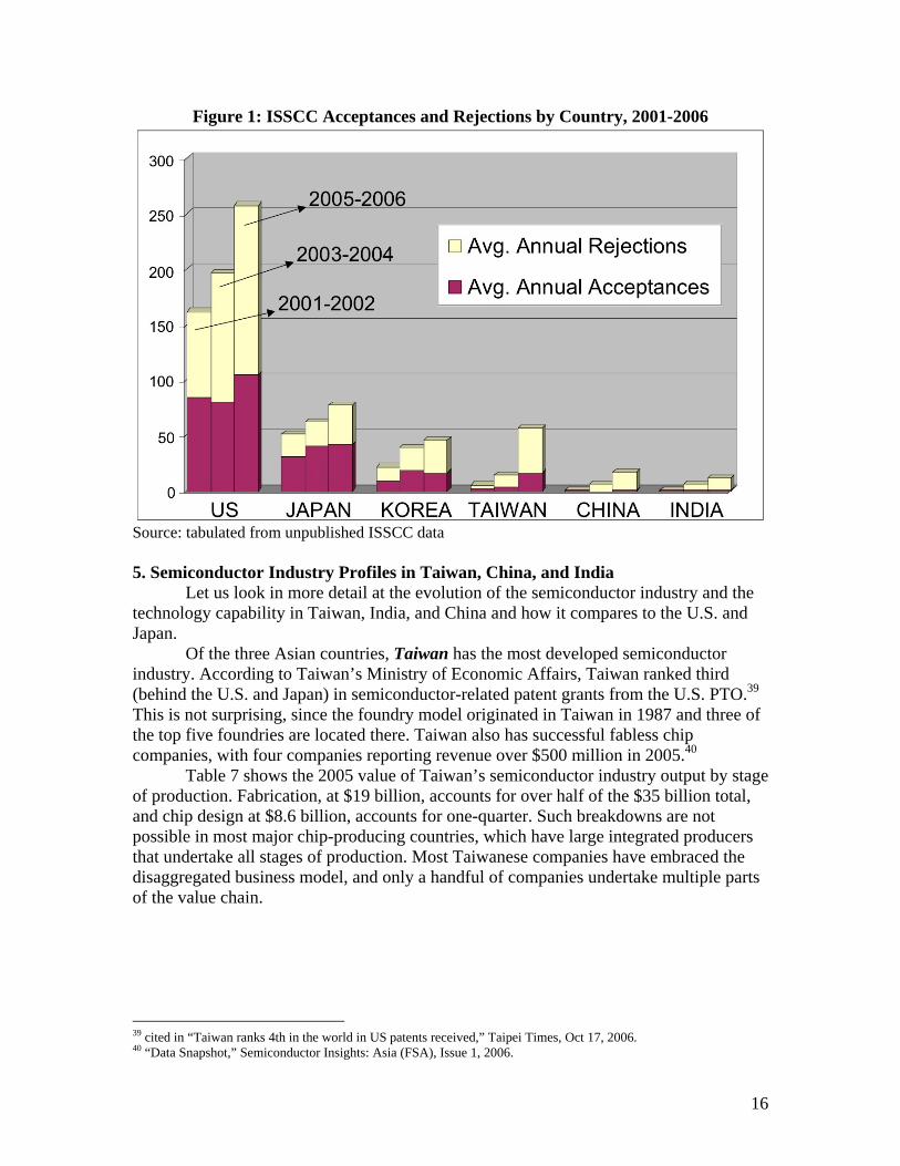
One measure of the capability of semiconductor design engineers, both in the universities and in companies, is the submission of papers to the International Solid-State Circuits Conference (ISSCC), which is IEEE’s global forum for presentation of advances in chip design (see Figure 1). This measure indicates that design capability in Asian countries has been improving. Over the 2001 to 2006 period, submissions from China, India, and especially Taiwan increased noticeably, as did the submissions from the U.S. As the conference’s overall acceptance rate fell from 53% to 38%, Taiwan’s total acceptances rose even as the rejection rate for Taiwan (and the U.S.) rose. We expect that acceptances from India and China will increase in the near future as the quality of their university engineering programs improves.
16
Figure 1: ISSCC Acceptances and Rejections by Country, 2001-2006
Source: tabulated from unpublished ISSCC data 5. Semiconductor Industry Profiles in Taiwan, China, and India
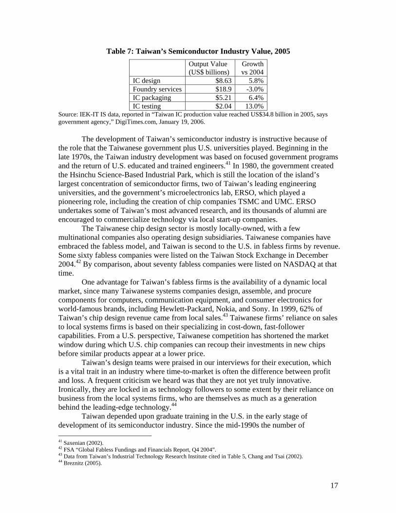
Let us look in more detail at the evolution of the semiconductor industry and the technology capability in Taiwan, India, and China and how it compares to the U.S. and Japan. Of the three Asian countries, Taiwan has the most developed semiconductor industry. According to Taiwan’s Ministry of Economic Affairs, Taiwan ranked third (behind the U.S. and Japan) in semiconductor-related patent grants from the U.S. PTO.39 This is not surprising, since the foundry model originated in Taiwan in 1987 and three of the top five foundries are located there. Taiwan also has successful fabless chip companies, with four companies reporting revenue over $500 million in 2005.40 Table 7 shows the 2005 value of Taiwan’s semiconductor industry output by stage of production. Fabrication, at $19 billion, accounts for over half of the $35 billion total, and chip design at $8.6 billion, accounts for one-quarter. Such breakdowns are not possible in most major chip-producing countries, which have large integrated producers that undertake all stages of production. Most Taiwanese companies have embraced the disaggregated business model, and only a handful of companies undertake multiple parts of the value chain.
39 cited in “Taiwan ranks 4th in the world in US patents received,” Taipei Times, Oct 17, 2006. 40 “Data Snapshot,” Semiconductor Insights: Asia (FSA), Issue 1, 2006.
17
Table 7: Taiwan’s Semiconductor Industry Value, 2005 Output Value
(US$ billions) Growth vs 2004
IC design $8.63 5.8%Foundry services $18.9 -3.0%IC packaging $5.21 6.4%IC testing $2.04 13.0%
Source: IEK-IT IS data, reported in “Taiwan IC production value reached US$34.8 billion in 2005, says government agency,” DigiTimes.com, January 19, 2006.
The development of Taiwan’s semiconductor industry is instructive because of the role that the Taiwanese government plus U.S. universities played. Beginning in the late 1970s, the Taiwan industry development was based on focused government programs and the return of U.S. educated and trained engineers.41 In 1980, the government created the Hsinchu Science-Based Industrial Park, which is still the location of the island’s largest concentration of semiconductor firms, two of Taiwan’s leading engineering universities, and the government’s microelectronics lab, ERSO, which played a pioneering role, including the creation of chip companies TSMC and UMC. ERSO undertakes some of Taiwan’s most advanced research, and its thousands of alumni are encouraged to commercialize technology via local start-up companies.
The Taiwanese chip design sector is mostly locally-owned, with a few multinational companies also operating design subsidiaries. Taiwanese companies have embraced the fabless model, and Taiwan is second to the U.S. in fabless firms by revenue. Some sixty fabless companies were listed on the Taiwan Stock Exchange in December 2004.42 By comparison, about seventy fabless companies were listed on NASDAQ at that time.
One advantage for Taiwan’s fabless firms is the availability of a dynamic local market, since many Taiwanese systems companies design, assemble, and procure components for computers, communication equipment, and consumer electronics for world-famous brands, including Hewlett-Packard, Nokia, and Sony. In 1999, 62% of Taiwan’s chip design revenue came from local sales.43 Taiwanese firms’ reliance on sales to local systems firms is based on their specializing in cost-down, fast-follower capabilities. From a U.S. perspective, Taiwanese competition has shortened the market window during which U.S. chip companies can recoup their investments in new chips before similar products appear at a lower price.
Taiwan’s design teams were praised in our interviews for their execution, which is a vital trait in an industry where time-to-market is often the difference between profit and loss. A frequent criticism we heard was that they are not yet truly innovative. Ironically, they are locked in as technology followers to some extent by their reliance on business from the local systems firms, who are themselves as much as a generation behind the leading-edge technology.44 Taiwan depended upon graduate training in the U.S. in the early stage of development of its semiconductor industry. Since the mid-1990s the number of 41 Saxenian (2002). 42 FSA “Global Fabless Fundings and Financials Report, Q4 2004”. 43 Data from Taiwan’s Industrial Technology Research Institute cited in Table 5, Chang and Tsai (2002). 44 Breznitz (2005).
18
Taiwanese receiving PhDs in engineering has declined steadily, and today few Taiwanese are obtaining graduate training in the U.S. Although PhD education has improved in Taiwan, we heard in our interviews in Taiwan some concern about the declining numbers of returnees from the U.S. Past returnees brought with them both graduate training and work experience that imparted management skills as well as practical knowledge. Taiwan’s government has instituted several programs to improve the local design sector, including a plan to train several thousand new design engineers in Taiwan’s universities, the creation of an exchange where local chip design houses can license reusable functional blocks, and an incubator where early-stage start-ups can share infrastructure and services.45 In 2001, the government began a renewed effort (Si-Soft) to improve local chip design capabilities. As part of the program, the faculty teaching chip design more than doubled from 200 in 2001 to more than 400 by 2005.46 Another initiative aims to attract chip design subsidiaries of major semiconductor companies, with early takers including Sony and Broadcom (a major U.S. fabless company). Following a model Taiwan has used successfully in other segments of the electronics industry, a government research institute created the SoC Technology Center (STC) in 2000 to design functional blocks that can be licensed to local companies. SoC, or system-on-a-chip, is a complex semiconductor that integrates multiple functions. The STC has over 200 engineers, most of whom have a Master’s degree or better.47 For the Taiwanese semiconductor industry, China presents both a challenge and an opportunity. The challenge comes from competition in the foundry and fabless sectors, especially for low-cost designs using older technologies, and from competition for engineering talent to work in China and bring with them their knowledge of advanced technology in design and manufacturing. The opportunity comes from the ability to partner with Chinese companies elsewhere in the value chain, so that Taiwanese companies can provide high-end design and manufacturing services, and from access to the rapidly growing markets in China. Political issues have been constraining the opportunities for companies to develop partnerships and markets in China, even as the companies experience the loss of experienced engineers to Chinese competitors. Currently Taiwan-born engineers are an important ingredient in the technology development that is occurring in China, in much the same way that the U.S. played a role in the earlier development in Taiwan. Although China seems to be benefiting more than Taiwan from the on-going flows of engineers, capital, and business activities between the two countries, this may change over time if official Taiwan government policy changes. China appears to be following the Taiwan pattern of industry development: government sponsorship, access to local system firms such as Haier, Huawei, and TCL that are increasingly engaged in global markets, and active involvement of expatriates returning from the United States or experienced engineers relocating from Taiwan.48
In little over a decade, Chinese firms have developed impressive fabrication capability, with the help of the Chinese government and of foreign companies as investors, technology licensors, or unwitting suppliers of experienced engineers and technology, as was the case in the SMIC hiring of TSMC engineers. Table 8 shows the
45 “Trends in SOC design unthaw at SOC 2004,” EDN, December 9, 2004. 46 Chikashi Horikiri, “Taiwan Transforms into IC Development Center,” Nikkei Electronics Asia, February 2006. 47 SoC Technology Center interview, March 2005. 48 Saxenian (2002).
19
main chip fabs in China, based primarily in Shanghai and more recently in Beijing. The most striking feature of the Chinese foundry business is that it is patterned on the Taiwanese foundry model—the foundries work under contract and do not design and manufacture their own products. The Chinese fabs are relatively small and have mature technologies.
U.S.-based chip companies have few high-profile deals with the China foundries—the major exception being Texas Instruments, which began working with Semiconductor Manufacturing International Corp (SMIC) in 2002 and added a deal to co-develop SMIC’s 90nm process in 2004.49 Executives with U.S. experience have also played key roles. For example, the CEOs of ASMC and HHNEC had previously worked at AMD.50
Table 8: Major Fabs in China, 2006 Company
Fab location
Year entered production
Capacity (wafers per month, 8-inch equivalent)
Advanced Semiconductor Manufacturing Corp (ASMC)
Shanghai 1995 25,000
Shanghai Hua Hong NEC Electronics (HHNEC)
Shanghai 1999 50,000
Semiconductor Manufacturing International Corp (SMIC)
Shanghai, Tianjin, and Beijing
2001 150,000
Grace Semiconductor Manufacturing Corp (GSMC)
Shanghai 2003 27,000
He Jian Technology Suzhou 2003 42,000
Taiwan Semiconductor Manufacturing Co (TSMC)
Shanghai 2004 15,000; (40,000 planned)
Source: iSuppli data, reported in Cage Chao and Esther Lam, “Despite China-based foundries reporting full utilization rates in 1Q, Taiwan players not overly impressed,” Digitimes.com, March 22, 2006 Apart from SMIC, China’s foundries have adopted modest growth plans, especially compared to the headline-grabbing predictions of a few years ago.51 But there is no question that chip fabrication is firmly established in China and will gradually expand. Although China’s fabs pose a growing low-cost challenge to the Taiwan foundries, from the perspective of U.S. chip firms they add welcome competition to the market for wafer processing.
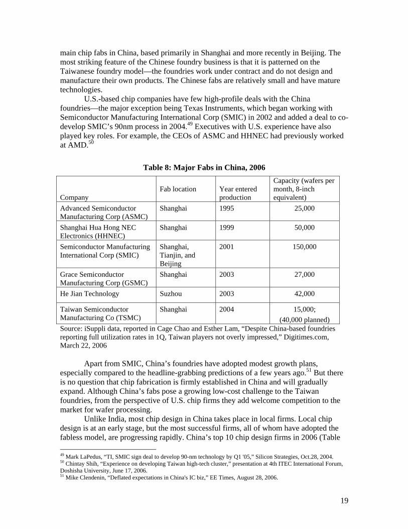
Unlike India, most chip design in China takes place in local firms. Local chip design is at an early stage, but the most successful firms, all of whom have adopted the fabless model, are progressing rapidly. China’s top 10 chip design firms in 2006 (Table 49 Mark LaPedus, “TI, SMIC sign deal to develop 90-nm technology by Q1 '05,” Silicon Strategies, Oct.28, 2004. 50 Chintay Shih, “Experience on developing Taiwan high-tech cluster,” presentation at 4th ITEC International Forum, Doshisha University, June 17, 2006. 51 Mike Clendenin, “Deflated expectations in China's IC biz,” EE Times, August 28, 2006.
20
9) had total revenue of $1.96 billion, up from $1.25 billion the year before.52 This is a fraction of chip consumption in China, which became the largest market of any region for chip consumption in 2005 with internal purchases of $40.8 billion.53
The largest of China’s fabless firms is Hong Kong-based Solomon Systech, which specializes in driver chips for low-end displays. The company, which was spun out from Motorola in 1999, has seen its revenue decline in recent years.
The second- and fourth-largest firms (Actions, media player chips and Vimicro, PC camera image processors) had IPOs on NASDAQ in 2005. Actions was spun out in 2001 from a Taiwanese company that withdrew from China, while Vimicro was founded by returnees with experience as Silicon Valley entrepreneurs following earlier experience at IBM, Hewlett-Packard, and Intel. Spreadtrum (telecom chips) was also founded by returnees.
The third- and fifth-ranked companies, Datang and HiSilicon, are linked to two of China’s largest telecommunications equipment companies, Datang Telecom and Huawei, respectively.
One of the earliest and largest applications for microchips in China are the relatively unsophisticated circuits used in smart cards. Huahong, Tongfang, CEC Huada and others are primarily involved in the smart card chip market.
Table 9: China's Top 10 Fabless Semiconductor Companies, 2006 2006 Rank
Company HQ City Year Established
Revenue ($ millions)
Change From 2005
1 Solomon Systech Hong Kong 1999 $254 -37% 2 Actions Zhuhai,
Guangdong 2001 $171 13%
3 Datang Microelectronics
Beijing 1996 $138 106%
4 Vimicro Beijing 1999 $130 37% 5 HiSilicon (formerly
Huawei ASIC Design Center)
Shenzhen, Guangdong
1991 $116 29%
6 Silan Hangzhou 1997 $112 40% 7 Spreadtrum Shanghai 2001 $107 167% 8 Huahong IC Shanghai 1998 $ 85 85% 9 Tongfang
Microelectronics Beijing 2001 $ 72 148%
10 CEC Huada (formerly China IC Design Center)
Beijing 1986 $ 68 94%
Others $707 Total $1,960 57% SOURCE: iSuppli data for 2006 revenue reported in Tech-On, Aug 20, 2007; miscellaneous sources for remaining columns 52 Ikutarou Kojima, “Chinese Fabless Semiconductor Manufacturers' Sales to Reach $2.8 Bil. in 2007: iSuppli,” Tech-On, Aug 20, 2007 and Mark LaPedus, “iSuppli lists China's top fabless IC rankings,” EE Times, April 21, 2006. 53 Mark LaPedus, “China becomes largest IC market,” EE Times, January 8, 2006.
21
In terms of process technology, which is one measure of sophistication, most Chinese chip design is still a generation or two behind fabless companies in the rest of the world. In 2006, 0.25-micron and 0.18-micron were considered mainstream, with a few companies reaching 0.13-micron.54 Elsewhere, the 0.09-micron generation was considered mainstream, and the leading edge had moved to 0.065-micron.55
The most advanced chip design by Chinese companies is being done by the design divisions of some of the local systems firms (most of which are not counted as fabless design companies) and a few world-class start-ups headed by U.S. returnees. The large and growing domestic market created by the local system firms provides the opportunity for China’s chip design companies to grow and become profitable, especially since market entry by foreign firms is constrained by the government. In the future, local design firms may be able to use their expertise and revenues gained from the large local market to design products for the global marketplace.
The Chinese government has taken many steps in support of chip design firms, some of the largest of whom are state-owned. Measures include tax reductions, venture investing, incubators in seven major cities, and special government projects.56 A value-added tax preference for domestically-designed chips was phased out under U.S. pressure, and will reportedly be replaced by a WTO-friendly R&D fund, although it has not been announced as of this writing (September 2006).57
The return of Chinese nationals with education and work experience has been an important part of China’s recent technology development.58 The returnees provide valuable management experience and connectivity to global networks that tend to accelerate the pace at which China’s chip sector can develop.59 The government maintains statistics on student returnees. In 2003, it was reported that, of 580,000 students that had gone abroad since 1978, one-quarter (or 150,000) had returned.60 These returnees had started 5,000 businesses, including over 2,000 IT companies in Beijing's Zhongguancun Science Park (one-sixth the park total).61 China is working to attract more high-tech returnees with a range of specially-targeted incentives and infrastructure.62 One factor that favors the development of local design companies is that engineers prefer to work for domestic start-ups and domestic companies rather than MNCs – virtually the opposite of what interviews revealed in india. Many young Chinese engineers, especially returnees, want to take the risk working for an emerging company that may result in great wealth.
54 “China’s Fabless Revenue Grows 55 Percent in 2006,” www.euroasiasemiconductor.com, March 2007. 55 Richard Goering, “Running start helps clear 90-nm hurdles,” EE Times, April 3, 2006. 56 “Synopsys Teams with China's Ministry of Science and Technology, SMIC,” Nikkei Electronics Asia, March 21, 2003; “An Uneven Playing Field,” Electronic News, July 3, 2003; “China nurtures home-grown semiconductor industry,” EBN, December 8, 2003; “China government to support Solomon Systech, Actions and Silan,” DigiTimes, April 14, 2005. 57 “China to form R&D fund to replace VAT rebate, says report,” EE Times, April 15, 2005. 58 Saxenian (2002). 59 “Story behind the Story: Design in China is growing, but not exploding,” audiocast by Bill Roberts, Electronic Business, September 1, 2006, http://www.edn.com/article/CA6368425.html?text=%22design+in+china%22# 60 “More overseas Chinese students returning home to find opportunities,” November 16, 2003, http://www.china-embassy.org/eng/gyzg/t42338.htm 61 “More overseas Chinese students return home,” January 1, 2004, http://www.china-embassy.org/eng/gyzg/t57364.htm 62 Mike Clendenin, “China starting to lure back its best brains,” EE Times, January 3, 2002.
22
India presents a very different picture than China in the semiconductor industry. India faces benign neglect by the government, a lack of manufacturing for chips and systems, and weaker levels of brain circulation with its U.S.-based expatriates.63 Unlike Taiwan and China, India has no high-volume chip manufacturing, although as many as five proposals to build a foundry are in various stages of negotiation.64 India is estimated to have 120 chip design firms, and its chip design revenue in 2005 is estimated to be $583 million.65 Most of this chip design is taking place in foreign subsidiaries, including most of the top 20 U.S. companies and many European companies. This flow of semiconductor engineering talent to multinationals slows down the diffusion of technology to local firms, although it lays the foundation for the potential creation of local companies if managers from MNCs decide to start their own firms. So far MNCs in India have had few instances where employees leave to start their own companies. However we heard of at least two cases of this occurring over the past two years at one U.S. subsidiary.66
Foreign chip companies have been attracted to India by Indian engineers’ knowledge of English and the successful Indian software sector. Many of the early Indian investments by chip companies were software-focused and involved writing the microcode that becomes part of the chip. Over time, the Indian affiliates have taken on a bigger role that can extend to complete chip designs from specification to physical layout. This transition can happen quite quickly. Intel, for example, opened a software center in Bangalore in 1999, then started building a design team for 32-bit microprocessors in 2002.67
So far, India has no major fabless companies designing chips for sale under their own brand. Domestic chip design companies mainly provide design services, which vary in their capabilities. Local design companies use a time and material-based pricing method, which allocates specific tasks to be carried out within set time lines and is easy to execute, according to an India Semiconductor Association (ISA) study.68 These companies tend to develop simple subsystems based on customer specifications. The larger independent firms offering VLSI design services, such as Wipro, Tata, and Sasken, are much more sophisticated. They use a fixed price method, are able to provide end-to-end solutions that incorporate in-house proprietary IP, and offer design services across the VLSI design flow. The government is developing policies to support domestic chip design firms.
In contrast to China, Indian engineers, according to our fieldwork, prefer multinationals and large local companies over local start-ups, since engineers and their family members do not tend toward taking risks and their Hindu values constrain pursuing and displaying wealth. However we also heard that the possibility of leaving a multi-national to start a company is slowly becoming more acceptable among Indians
63 Saxenian (2002). 64 Russ Arensman, “Move over, China,” Electronic Business, March 2006. 65 Data from Frost & Sullivan, in Chitra Giridhar, “India design firms as product innovators,” Electronic Business, July 18, 2006. 66 Personal communications in Bangalore, November 2005. 67 “Intel, TSMC Set Up Camps In Developing Asian Markets,” WSJ.com, August 30, 2002. 68 “Study: Indian design firms prefer time and material model”, EE Times, Sept 22, 2006.
23
engineers, whose personal motivation is often given as helping India develop rather accumulating personal wealth.69 The U.S. MNCs are highly dependent upon returnees with advanced degrees from the U.S. to develop new projects in India, since most domestically-trained engineers lack the knowledge of the technology being transferred, lack the management skills required, and also lack knowledge of the entire product cycle. Foreign subsidiaries are facing formidable problems in their operations in India, including a very tight labor market and inadequate infrastructure in transportation, communications, and housing. As in China, the quality of engineering graduates is highly variable. This is exacerbated in India by the fact that most engineers want to study computer science rather than electronics, and many are not aware of the job opportunities in semiconductors. Graduate education in EE is in its infancy, and doctoral education in the seven major technical universities is not up to U.S. standards. The very low wages paid to professors, the lack of expensive and ever-changing EDA tools, and the difficulty and expense in getting engineering chips fabricated, partly explain the problems in developing world-class graduate education. In addition, India has not attracted returnees to the extent that China has, and so the flow of returnees with graduate degrees is low. The low flow of new domestic graduates and returnees into the EE labor supply, coupled with the need for at least three to five years of experience to be a fully-productive chip designer, has prevented the supply of design engineers from keeping up with the fast-growing demand. As a result, wages for chip designers have been rising rapidly, both at entry level and during the first five years (and beyond). As mentioned above, salaries after five years of experience are double the entry-level salary. Inadequate infrastructure, especially in Bangalore, also imposes serious problems for chip design centers. The lack of a stable energy supply and lack of office space means that foreign subsidiaries must make substantial investments to provide both offices and reliable electricity. The small, pothole-filled roads are gridlocked in Bangalore, the country’s primary city for high-tech, and employees spend long hours in commuting from affordable housing. In addition, high-tech companies are spread out over the city, and commuting between companies, or even between company locations, is very time consuming. The housing stock has not kept up with growth, and housing prices and rents have been rising rapidly. Many employees are faced with the choice of living in inadequate housing or living far from work. The housing and schooling problems are especially severe for the returnees from the U.S., who want to replicate the quality of housing and schools their families experienced in the United States. In Bangalore, we were told by several executives that their cost of living was almost as high in Bangalore as in the U.S. because of the high cost of housing and international schools.70 The shortage of engineering talent and weak infrastructure is constraining how fast the semiconductor design industry, both for foreign subsidiaries and local companies, can grow in India, especially in Bangalore. Some companies have been moving operations to areas that are not as expensive as Bangalore and have better infrastructure. However the talent shortages still remain, especially for experienced engineers with advanced degrees.
69 Personal communications in Bangalore, November 2005. 70 Personal communications in Bangalore, November 2005.
24
6. The Outlook for the Semiconductor Industry by Country Overall the U.S. semiconductor industry has benefited from globalization, which
has allowed companies to lower costs by moving operations or subcontracting. In turn, the lower costs have allowed U.S. multinationals to expand the market for their products and to compete with foreign companies that are more efficient or face lower domestic costs or receive government subsidies. U.S. chip industry has also benefited from a large talent pool, which is primarily produced by U.S. world-class universities, and by the U.S. market, which is still the largest in the world. U.S. universities and companies have taken advantage of the brain circulation and of the innovation produced by the linkages between the universities and companies, both mature and start-ups. For the U.S., start-ups have played a critical role in product innovation, both as a source of new technology to mature companies through acquisition or licensing, and to the industry with breakthrough technologies that lead to successful public companies, such as Cisco and Qualcomm.
However danger signs point to problems that the chip industry and its workers may face in the near term. A major challenge for the U.S. is the state of the domestic economy, which has relied on foreign countries and foreigners to provide savings to pay for public and private debts, which were compounded by the housing mortgage crisis. Over time a low domestic savings rate puts upward pressure on interest rates, which lowers private investment and weakens economic growth.
At the same time, U.S. companies must expand in the rapidly growing markets in Asia. Fortunately a realignment of the U.S. dollar with foreign currencies is helpful in making U.S. companies more competitive abroad, but this by itself is not adequate develop products for customers in developing markets, who have different needs and values than U.S. consumers.
A potential problem for the U.S. is its dependence on foreign students for graduate training in U.S. universities, since after graduation these engineers may become increasingly mobile across the globe. If so, U.S. companies may find their access to top talent becomes more unreliable. The lack of integration of immigration policy with higher education policy impedes the ability for the government, universities, and companies to find acceptable solutions that will ensure a steady supply of the best-trained engineers to domestic companies. Foreign graduates of U.S. universities find that they must qualify for a temporary visa (usually H-1B visa) through an employer in order to work in the U.S. after earning a Masters or PhD. However their visa problems do not end there, since the H-1B allows them to work for their employer for up to six years (with one renewal). If the H-1B visa holders have not been able to obtain permanent residency (a “green card”), which now takes more than five years to obtain, these highly educated and skilled workers are forced to return to their home countries.
Hidden discrimination against ethnic groups, who hit glass ceilings in many large U.S. companies, has also pushed many of them back to their home countries, where their opportunity to start new companies, especially in China, or to work for multinational companies, especially in India, provides them with superior careers over the alternative of stagnation in middle management in the U.S. Others may strike out as entrepreneurs in the United States, where they have succeeded. 71 We expect the proportion of foreign
71 AnnaLee Saxenian, The New Argonaut: Regional Advantage in a Global Economy. Cambridge: Harvard University Press, 2006.
25
engineers who return home after being educated and working in the U.S. to grow, and the U.S. may face a brain drain with its current higher education and immigration policies.
Japanese semiconductor companies have been slower to take advantage of
locating activities in lower cost regions in Asia, even though areas are closer to home. This reflects the Japanese preference for keeping manufacturing operation (and jobs) in Japan. This also reflects language barriers in India and China, where English is more likely to be spoken than Japanese as well as cultural barriers in China, where Japanese actions during World War II still cause bitter memories. Japanese electronics companies had relied far too long on their large (but relative shrinking) domestic market, while companies in other countries were expanding their sales abroad. Reliance on the Japanese market became a problem especially during the “lost decade” of the 1990s when Japan suffered slow or negative growth.
In the 2000s, Japanese companies began in earnest to set up manufacturing and assembly operations in China and Taiwan, both to take advantage of the lower costs and to develop a presence in the large rapidly growing market. Established Japanese electronics companies, which had high status in hiring and product promotion in Japan as long as the companies were doing well, continued to rely primarily upon internal R&D for innovation, although Japan’s multinational electronics companies relied upon alliances and networks to push ahead in the innovation process as costs and risks increased. Large Japanese companies presented a barrier to entrepreneurs who wanted to found start-ups to develop new technology, since the large companies would not purchase products from new companies and so start-ups could not break into the domestic market.
Japan’s isolation extended to the university system, which draws largely from a domestic population, which tends to do both undergraduate and graduate training at home. Partly because of language barriers and partly because of preferences, Japan has remained on the periphery of the brain circulation of professional workers that has been a vital part of the start-up and innovation process in the U.S.
Japan’s economic upturn has returned the semiconductor and electronics companies to profitability and provides them with new opportunities to expand into new product market both at home and abroad. Unfortunately, their expanded investment has been disproportionately to build new 300mm fabs, which have generally been operating at throughputs that do not take advantage of economies of scale (the main except being Toshiba). However Japanese expansion of manufacturing operations in China, and more recently design operations in India, indicates that Japan may finally be able to take advantage of the rapid growth of both regional talent and product markets. We believe that Japan’s future depends upon her ability to play a key role in the integration and development of regional markets. In our fieldwork, we observed more willingness by younger Japanese to travel and work in China and Taiwan, as well as to have colleagues from those countries work in Japan. The overlap of written Chinese and Japanese presents less of a barrier than the spoken language, and younger Japanese seem more open to learning Chinese.
Taiwan’s success in building the foundry business and an electronics component industry over the past three decades, is envied by emerging Asian rivals. The role of the government, which set up effective research centers and spawned new companies, and of
26
returnees, who were educated and then worked in the U.S., were critical in the early stages of Taiwan’s industrial development. Taiwan’s development rested upon a well-executed fast follower model that competed on cost and drew on the country’s well-trained technical workers, government-subsidized R&D, and large number of original equipment manufacturers (OEMs). As we saw, however, Taiwan’s challenge is to move beyond the fast-follower model to develop leading-edge technology and products that compete on design as well as price. OEMs may actually support the development of start-ups with a fast-follower (as opposed to leading-edge) strategy because their products use legacy technology and rely on a low-price advantage. Start-ups that develop leading-edge technology or products may have a hard finding customers quickly enough to produce the required revenues for sustainable returns. Taiwan’s universities are building graduate engineering programs to develop leading-edge technology as it trains engineers to conduct research. Yet this process requires time as well as funding, and requires establishing new linkages between the university and company R&D programs. We think that the universities must, and will, play a vital role in the future innovation process in Taiwan, and that Taiwan will continue to draw on its synergy with China, where Taiwan supplies expertise and high-end design and technology to Chinese companies, who help develop products and manufacture them. However China poses a potential threat to Taiwan, both as a “fast follower” competitor and as low-cost foundry competitor. Taiwanese companies must continue to move to higher-end design and manufacturing activities as it benefits from using China for lower-end lower-cost activities.
China and India present an interesting contrast in their approaches to development in high-tech industries. India has developed expertise that primarily complements the activities of developed countries, especially the U.S. We saw this in India’s development of design centers that primarily undertook lower-end activities in the design flow or updated legacy designs. China has undertaken a more ambitious route of supporting start-ups that would compete directly with semiconductor companies globally, and of developing a foundry business that would compete with established foundries, especially in Taiwan. Chinese companies have become the manufacturing center of the world, and this is true in electronics as well as across a wide array of industries.
Chinese companies have taken advantage of ties to Taiwan, especially in recruiting engineering and managerial talent and in attracting investment capital. Some tactics used by Chinese companies in acquiring expertise and technology have been illegal, as when SMIC hired engineers from TSMC who smuggled in proprietary technology. Other Chinese companies have been accused of illegally using designs and technology without licensing them.
Chinese companies have benefited from their large growing market that is protected by the Chinese government through a variety of standards and regulations that are embedded in a bureaucratic maze. In addition, Chinese financial markets are regulated, both its exchange rate with the dollar and the external currency flows. In contrast, India has experienced a slower growth rate in an economy that is now much more open to the global economy. Government planning plans a smaller role in India than in China, because democracy often slows down the process. For example, the building of roads in Bangalore is severely hampered by popular protests, especially of squatters who would be displaced.
27
Both India and China are held back by their lack of graduate education and by their underdeveloped financial and political systems. China is developing higher education at a very rapid pace, especially by attracting world-class professors who are attracted back to well-paid academics jobs in China. India’s efforts to develop graduate education are hampered by low salaries and lack of public support for graduate education compared to other competing demands on public resources. In general, India’s ability to use public resources to push high-tech development plans are severely hampered by competing demands and a slow bureaucracy, as their years-long and continually-changing government program to support chip manufacturing shows. China faces different constraints from its Communist system. Although the government can move forward on projects and plans without public support, the political system is fragile with the enormous income and lifestyle differential between the citizens of the urban coastline and the rural interior, which is causing resentment and potential unrest.
Whether their activities complement or compete with the activities of other countries, becoming part of a global value chain has been an important step in the integration of the Chinese and Indian companies into the global economy. This global integration supports the rapid growth of their potentially large markets. In return, U. S. semiconductor companies have benefited from integrating low-cost manufacturing in China and low-cost design in India into their supply chains, and U.S. companies are learning how to develop and sell goods to the growing markets in India, and especially China. How quickly China or India can move up the technology curve and expand into global markets remains to be seen. These two countries will play an increasingly important role in high-tech industries, both as markets and suppliers. Although neither country will overtake the U.S. in the semiconductor industry in the near future, their long-run challenge U.S. semiconductor leadership remains to be seen.