Embed Size (px)
Citation preview
Semiconductor nanowires as a bottom-up approach to realize nanoelectronic and nanophotonic devices
Lars Samuelson
Lund University, Solid State Physcis/the Nanometer Structure Consortium, Box 118, S-221 00 Lund, Sweden E-mail: [email protected]
Abstract-In this presentation will be given an up-date of the status of epitaxially grown III-V nanowires, from the perspective of growth, processing, physics and applications in the areas of nanoelectronics and nanophotonics
I. INTRODUCTION
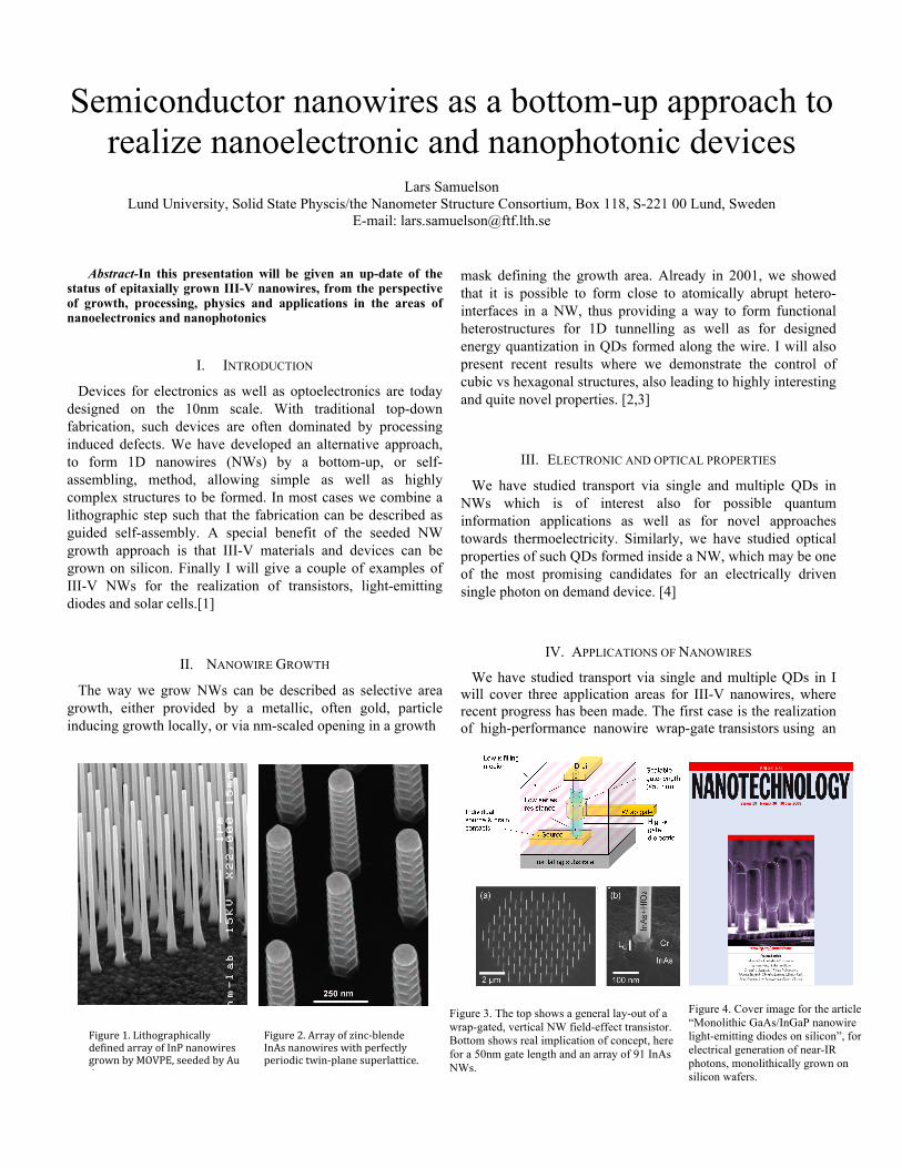
Devices for electronics as well as optoelectronics are today designed on the 10nm scale. With traditional top-down fabrication, such devices are often dominated by processing induced defects. We have developed an alternative approach, to form 1D nanowires (NWs) by a bottom-up, or self-assembling, method, allowing simple as well as highly complex structures to be formed. In most cases we combine a lithographic step such that the fabrication can be described as guided self-assembly. A special benefit of the seeded NW growth approach is that III-V materials and devices can be grown on silicon. Finally I will give a couple of examples of III-V NWs for the realization of transistors, light-emitting diodes and solar cells.[1]
II. NANOWIRE GROWTH
The way we grow NWs can be described as selective area growth, either provided by a metallic, often gold, particle inducing growth locally, or via nm-scaled opening in a growth
mask defining the growth area. Already in 2001, we showed that it is possible to form close to atomically abrupt hetero-interfaces in a NW, thus providing a way to form functional heterostructures for 1D tunnelling as well as for designed energy quantization in QDs formed along the wire. I will also present recent results where we demonstrate the control of cubic vs hexagonal structures, also leading to highly interesting and quite novel properties. [2,3]
III. ELECTRONIC AND OPTICAL PROPERTIES
We have studied transport via single and multiple QDs in NWs which is of interest also for possible quantum information applications as well as for novel approaches towards thermoelectricity. Similarly, we have studied optical properties of such QDs formed inside a NW, which may be one of the most promising candidates for an electrically driven single photon on demand device. [4]
IV. APPLICATIONS OF NANOWIRES
We have studied transport via single and multiple QDs in I will cover three application areas for III-V nanowires, where recent progress has been made. The first case is the realization of high-performance nanowire wrap-gate transistors using an
!
!
!"#$%&'!()!*#+,-$&./,#0.112!3'4#5'3!.&&.2!-4!657!5.5-8#&'9!$&-85!:2!;<=7>?!9''3'3!:2!@%!
3#909)!
"#$%&'!A)!@&&.2!-4!B#50C:1'53'!65@9!5.5-8#&'9!8#+,!/'&4'0+12!/'&#-3#0!+8#5C/1.5'!9%/'&1.++#0')!
Figure 3. The top shows a general lay-out of a wrap-gated, vertical NW field-effect transistor. Bottom shows real implication of concept, here for a 50nm gate length and an array of 91 InAs NWs.
Figure 4. Cover image for the article “Monolithic GaAs/InGaP nanowire light-emitting diodes on silicon”, for electrical generation of near-IR photons, monolithically grown on silicon wafers.
InAs nanowire surrounded by a high-K dielectric and a wrap-around metallic gate. This constitutes an ideal system for co-axial electrostatic control of the conducting channel. The second case I will present is a couple of different light-emitting structures, involving either single QDs as mentioned above, GaAs/InGaP IR-emitting LEDs as well as nitride based NWs for shorter wave-length emission. Finally, I will show very recent progress in making pn-junctions and Esaki-diodes in InP-based NWs for use in solar cells. [5, 6]
V. CONCLUSIONS
NWs are now ready to take the step from being a promising approach to grow materials to being seriously considered for electronics and optoelectronics.
ACKNOWLEDGMENT
This research is indeed the achievement of many students, Post-docs and senior researchers, also in our start-up companies QuNano AB, QuMat Technology AB, GLO AB and Sol Voltaics AB, as well as in EU-funded projects NODE (“Nanowire-based One-Dimensional Electronics”) and AMON-RA (“Architectures, Materials & One-dimensional Nanowires for Photovoltaics – Research & Applications”), with everyone involved gratefully acknowledged for their contributions.
REFERENCES [1] L. Samuelson et al., “Semiconductor nanowires for 0D and 1D physics
and applications” , Physica E 25, 313, (2004) [2] P. Caroff et al., “Controlled polytypic and twin-plane superlattices in III-V
nanowires”, Nature Nanotechn. 4, 50 (2009) [3] M.T. Björk et al., “One-dimensional steeplechase for electrons realized“,
Nano Letters 2, 87 (2002) [4] N. Sköld et al., “Microphotoluminescence studies of tunable wurtzite
InAs0.85P0.15 quantum dots embedded in wurtzite InP nanowires”, Phys Rev B 80, 041312(R) (2009)
[5] C. Thelander et al., “Vertical enhancement-mode InAs nanowire FET with 50nm wrap gate”, IEEE-EDL 29, 206 (2008)
[6] C.P.T. Svensson et al., “Monolithic GaAs/InGaP nanowire light-emitting diodes on Si”, Nanotechn 19, 305201 (2008)