Embed Size (px)
Citation preview

Semiconductor R&D advances for improved energy
efficiency with applications at home and on the road
Hans Stork
Senior VP and CTO

2 • H. Stork March 2012
• Headquarters: Phoenix, AZ
• Employees: ~20,000 globally
• Revenue: ~$3.4Bn(1)
• Market Capitalization: ~$4.3Bn(2)
• Ticker: ONNN
• Founded: Spun-off from Motorola 1999, IPO 2000
ON Semiconductor Today
(1) Based on 2011 annual revenue.
(2) Based on closing stock price on February 9, 2012
(3) Sector % based on 2011 results

3 • H. Stork March 2012
Successful Acquisitions Expand Solutions in Target Markets
20072006
October 10, 2008
May 15, 2006
Oregon Fabrication Facility
June 9, 2010November 4, 2009
December 31, 2007
CPU Voltage and PC
Thermal
Monitoring Business
March 17, 2008
January 27, 2010 January 1, 2011
2008 2009 2010 2011
February 27, 2011
CMOS Image Sensor
Business Unit

4 • H. Stork March 2012
ON Semiconductor products are found in ….
Computer 20%
Communications 20%
Consumer 13%
Automotive 20%
Industrial/Military/
Aerospace/Medical 27%
• Engine control
• Fuel injection
• Lighting
• Power locks/seats
• Smart grid communications
• Industrial automaton &
controls
• Aircraft / satellite
• Hearing aids
• Medical implants • Appliance motor drivers
• TV backlights
• Digital A/V switching &
transmission
• Cell phone battery
charging and protection
• Cell phone ESD
protection and
ElectroMagnetic
Interference Filtering
• Telecom clock generation
• AC-DC power supply
• Power regulation for
microprocessors
• Thermal protection

5 • H. Stork March 2012
Leadership Position in Focus End-Markets
Industrial ASIC#1
Power Adapters (ACDC)#1
Inverter HIC#2
Protection#1
Op Amp#1
Linear VREG#1
Analog ASIC (Non Auto)#2
Hearing Aid SOC#1
Computing
LED Lighting Smart Grid
Wired & Wireless
Comm.
Industrial /
Medical /
Mil-Aero
AutomotiveConsumerPC Core Power (DCDC)#1

6 • H. Stork March 2012
Capacity Investment ContinuesWafer Fab Increases ATO Capacity Increases

7 • H. Stork March 2012
CMOS/BCD Technology Portfolio
ON
C1
8M
S
I3T
25
, I3
T5
0, I3
T8
0
100 V
80 V
65 V
40 V
20 V
12 V
5 V
3.3 V
2.5 V
1.8 V
1.2 V
Vo
lta
ge
(V
ds
)
1.0 µm 0.7-0.8 µm 0.5-0.6 µm 0.35 µm 0.25 µm 0.18 µm 130 nm 110 nm 90 nm
(Technology Node)
BCD
CMOS
D3
L5
PS
5LV
PS
5A
,B
AC
MO
S2
VH
VIC
3 7
00
V
C5
ONBCD
25
ONC25
I2T
10
0
C8
ON
C11
0
ON
C3
5E
E
G10,C9,C3
Memory
ON
C1
8E
EO
NC
18
D
I4T
Fa
mil
y
Develop
8 • H. Stork March 2012
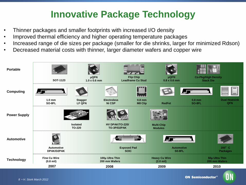
• Thinner packages and smaller footprints with increased I/O density
• Improved thermal efficiency and higher operating temperature packages
• Increased range of die sizes per package (smaller for die shrinks, larger for minimized Rdson)
• Decreased material costs with thinner, larger diameter wafers and copper wire
Portable
Computing
Power Supply
Automotive
Technology
2007 2008 2009 2010
Fine Cu Wire
(0.8 mil)
100μ Ultra Thin
200 mm Wafers
Heavy Cu Wire
(2.0 mil)
50μ Ultra Thin
200 mm Wafers
Automotive
DPAK/D2PAK
Exposed Pad
SOIC
Automotive
S0-8FL
200°C
Packages
Isolated
TO-220
HV DPAK/TO-220/
TO-3P/D2PAKMulti-Chip
Modules
1.0 mm
SO-8FL
Stagger
LF QFN
Electroless
Ni CSP
0.8 mm
M8 Clip RedFet
0.8 mm
SO-8FL
Dual Heatsink
QFN
SOT-1123μQFN
1.0 x 0.6 mm
Flip Chip
Leadframe Cu Stud
μQFN
0.8 x 0.6 mmCo-Pkg/High Density
Stack Die
Innovative Package Technology

9 • H. Stork March 2012
Automotive growth driven by higher sales in the US and emerging economies, and higher semi content per vehicle
Computing segment has the largest TAM; Notebooks and emerging markets drive category growth; Ultrabooks launch to counter potential media tablet cannibalization
Migration to variable speed motors for improved energy efficiency in White Goods presents growth opportunity in Consumer
LED lighting and smart meter deployment lead growth in the Industrial segment
Smartphones and Media Tablets drive growth in wireless; Networking / Telecom grow on increased mobile data consumption
2011 – 2014 Market Outlook
Source: TAM – Gartner Dec’11, iSuppli Dec’11, Strategy Analytics Jun’11
Industrial includes mil-aero and medical; Media Tablets are in Communications (Wireless)
TAM Revenue ($M) 2011 2012 2013 2014 CAGR
Automotive 23,709 27,469 30,431 33,260 11.9%
YonY 15.9% 10.8% 9.3%
Computing 117,131 117,258 129,310 127,808 3.0%
YonY 0.1% 10.3% -1.2%
Consumer 51,700 51,379 51,947 53,124 0.9%
YonY -0.6% 1.1% 2.3%
Industrial 29,053 31,169 35,357 41,637 12.7%
YonY 7.3% 13.4% 17.8%
Communications 84,041 90,451 100,101 106,493 8.2%
YonY 7.6% 10.7% 6.4%
0
20,000
40,000
60,000
80,000
100,000
120,000
140,000
2011 2012 2013 2014
Mill
ion
s $
Segment Revenue
Automotive Computing Consumer Industrial Communications
0.0%
2.0%
4.0%
6.0%
8.0%
10.0%
12.0%
14.0%
CAGR
2011 - 2014 TAM CAGR
Automotive Computing Consumer Industrial Communications
10 • H. Stork March 2012
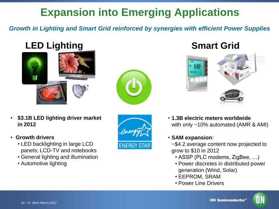
Expansion into Emerging Applications
• $3.1B LED lighting driver market
in 2012
• Growth drivers
• LED backlighting in large LCD
panels; LCD-TV and notebooks
• General lighting and illumination
• Automotive lighting
Growth in Lighting and Smart Grid reinforced by synergies with efficient Power Supplies
• 1.3B electric meters worldwide
with only ~10% automated (AMR & AMI)
• SAM expansion:
~$4.2 average content now projected to
grow to $10 in 2012
• ASSP (PLC modems, ZigBee, …)
• Power discretes in distributed power
generation (Wind, Solar)
• EEPROM, SRAM
• Power Line Drivers
LED Lighting Smart Grid

11 • H. Stork March 2012
LED Lighting Content
• LED Drivers (120 and 240 Vac,
Medium Voltage AC and DC,
Battery Powered)
• Ambient Light Sensors
• Communication (PLC modems)
• Thermal Management Products
• Power Factor Controllers
• AC-DC and DC-DC Controllers
• Charge Pumps and
Inductive Drivers
• Constant Current Regulators
• Protection and Shunts
• MOSFETs and Rectifiers
Offline High Power Factor Triac Dimmable
LED Driver Intended for ENERGY STAR®
Commercial and Residential LED Luminaires• Active mode efficiency ~83% at 12 W Pout
• Dimmable to less than 2% with standard Triac
Dimmers
• Power Factor > 0.97 typical at full load
• Typical Total Harmonic Distortion < 10%

12 • H. Stork March 2012
Smart Grid Segmentation
Applications
Smart Appliances
Applications
Smart HomeDistributed Sources of Energy
(Solar)Smart Meters
Controller / Thermostat
In Home Display
Charging Stations
Junction Boxes
Solar Shingles
Thin Film Panels
PV Panels
Concentrating
Solar Arrays
Inverters
Smart Meters
Communications Modules
for Smart Meters
Applications
13 • H. Stork March 2012
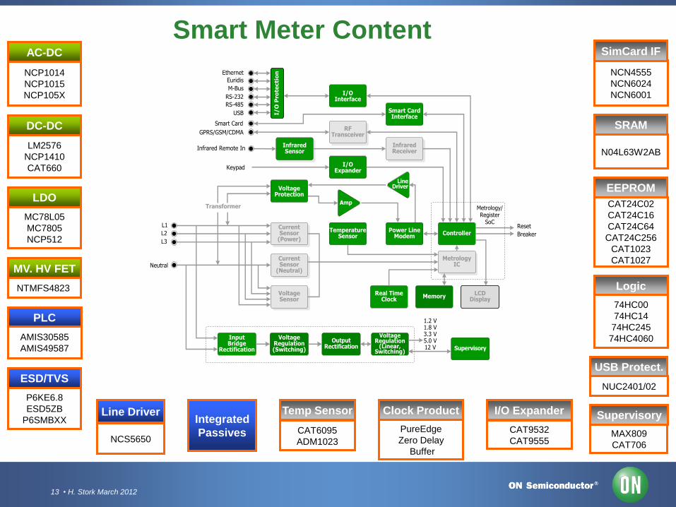
DC-DC
LM2576
NCP1410
CAT660
LDO
MC78L05
MC7805
NCP512
Supervisory
MAX809
CAT706
EEPROM
CAT24C02
CAT24C16
CAT24C64
CAT24C256
CAT1023
CAT1027
I/O Expander
CAT9532
CAT9555
ESD/TVS
P6KE6.8
ESD5ZB
P6SMBXX
Logic
74HC00
74HC14
74HC245
74HC4060
AC-DC
NCP1014
NCP1015
NCP105X
PLC
AMIS30585
AMIS49587
Temp Sensor
CAT6095
ADM1023
Line Driver
NCS5650
SRAM
N04L63W2AB
NCN4555
NCN6024
NCN6001
SimCard IF
Clock Product
PureEdge
Zero Delay
Buffer
Smart Meter Content
USB Protect.
NUC2401/02
NTMFS4823
MV. HV FET
Integrated
Passives
Real Time Clock
Supervisory
I/O
Pro
tecti
on
Line DriverVoltage
Protection
Amp
Smart Card Interface
ControllerCurrent Sensor
(Power)
I/O Interface
Current Sensor
(Neutral)
LCDDisplay
I/O Expander
Voltage Sensor
Infrared Receiver
RF Transceiver
Voltage Regulation
(Linear, Switching)
Breaker
RS-485
L1
Neutral
Keypad
Infrared Remote In
RS-232
GPRS/GSM/CDMA
Smart Card
ResetPower Line
Modem
OutputRectification
InputBridge
Rectification
Voltage Regulation(Switching)
Transformer
USB
Ethernet
Euridis
M-Bus
L2
L3
Metrology IC
Memory
1.2 V1.8 V3.3 V5.0 V12 V
Metrology/Register
SoC
Temperature Sensor
Infrared Sensor

14 • H. Stork March 2012
Solar Content
Bypass Diodes for Modules
Co-packed IGBT
and HV Rectifier
for Inverter
Trench Ultrafast
for PFC Boost
Diode
HV MOSFET or
IGBT for PFC
Switch
15 • H. Stork March 2012
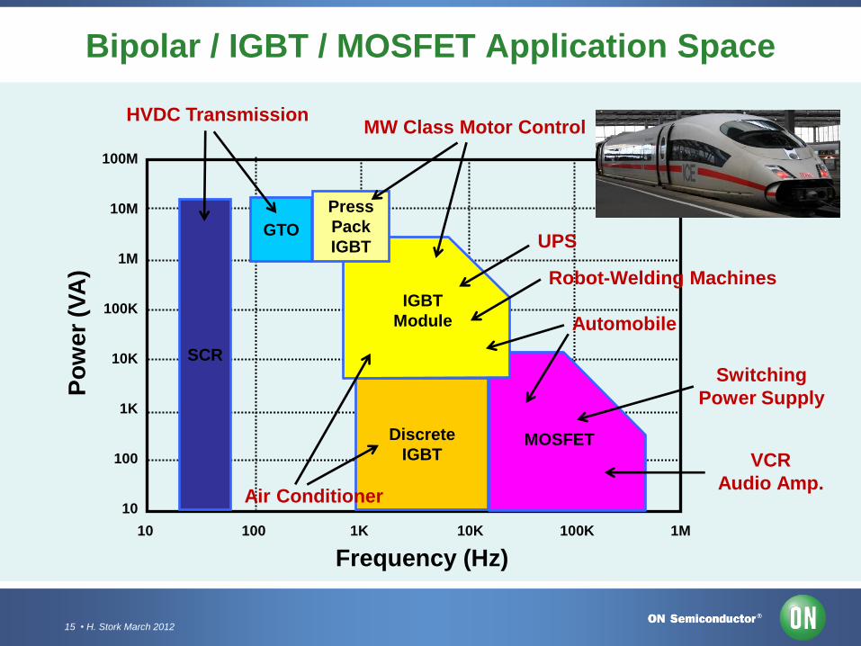
Bipolar / IGBT / MOSFET Application Space
Frequency (Hz)
Po
wer
(VA
)
10 100 1K 10K 100K 1M
100M
10M
1M
100K
10K
1K
100
10
MOSFETDiscrete
IGBT
IGBT
Module
Press
Pack
IGBTGTO
SCR
HVDC Transmission
Robot-Welding Machines
Automobile
Switching
Power Supply
UPS
VCR
Audio Amp.Air Conditioner
MW Class Motor Control

16 • H. Stork March 2012
LV-Power MOSFET Applications
Ultrasonic
Medical
appliance
MD
Machine Tool
Power Supply
For Machine
Processing
Actuator
for Industrial
low loss,
high
reliability
1u 10u 100u 1m 10m
Load Inductance L (H)
Op
era
tin
g F
req
uen
cy
f (H
z)
10M
1M
100K
10K
1K
Small Motor
Drive
(HDD, Printer)
improved start-up
performance,
reduced loss, size
low loss
high accuracy
control
Common Needs:
• Energy savings
• Low noise, EMC
• Small & slim package
AC- DC
Switching
Power Supply
(Network OA,
Basestation)
Motor
Drive for
Industrial
(FA inverter) Automotive Electronic
Components
(ABS, injection, solenoid)
high density,
high speed,
processing
high speed,
high accuracy
graphics proc.
high speed
processing
low loss
reduced voltage,
Loss, noise
DC-DC
Converter
(VRM, PC)
Telecom

17 • H. Stork March 2012
LV-MOSFET Roadmap
Planar
1990 1995 20052000
Trench Gen 1
Trench Gen 2
Trench Gen 3
Rdsonspec
scaling
Rdson.Qgd
scaling
2010
PlanarPlanar
1990 1995 20052000
Trench Gen 1Trench Gen 1
Trench Gen 2Trench Gen 2
Trench Gen 3Trench Gen 3
Rdsonspec
scaling
Rdson.Qgd
scaling
2010

18 • H. Stork March 2012
Devices for MHz SMPS Solutions
• Traditional Trench FETs cannot switch fast enough to meet higher frequency VR requirements
• Switching losses are dominant loss factors
• Innovative RF Power technology is used to meet the needs of high frequency VRMs
This solution
Low Side FET
High Side FETDriver IC
Clip Interconnect
6 mm
5 MHz High Efficiency DC-DC Converter Module
6 mm
1/9

19 • H. Stork March 2012
MV-MOSFET Ron and Ron*Qgd Scaling
n-e
pi
n-e
pi
n-e
pi
gate
gate
gate
gate
BLN = drain
p-body p-body p-body
Source terminal
Tre
nch
oxi
de
Thin gate oxide
n-e
pi
n-e
pi
n-e
pi
gate
gate
gate
gate
BLN = drain
p-body p-body p-body
Source terminal
Tre
nch
oxi
de
Thin gate oxide
Trench
Gate & Field Plate
Planar
1990 1995 20052000 2010
Trench Split Gate
& Field Plate
Trench Gate
Rdson.Qgd
scaling
Rdsonspec
scaling
XtreMOSTM
n-e
pi
n-e
pi
n-e
pi
gate
gate
gate
gate
BLN = drain
p-body p-body p-body
Source terminal
Tre
nch
oxi
de
Thin gate oxide
n-e
pi
n-e
pi
n-e
pi
gate
gate
gate
gate
BLN = drain
p-body p-body p-body
Source terminal
Tre
nch
oxi
de
Thin gate oxide
Trench
Gate & Field Plate
n-e
pi
n-e
pi
n-e
pi
gate
gate
gate
gate
BLN = drain
p-body p-body p-body
Source terminal
Tre
nch
oxi
de
Thin gate oxide
n-e
pi
n-e
pi
n-e
pi
gate
gate
gate
gate
BLN = drain
p-body p-body p-body
Source terminal
Tre
nch
oxi
de
Thin gate oxide
Trench
Gate & Field Plate
PlanarPlanar
1990 1995 20052000 2010
Trench Split Gate
& Field Plate
Trench Split Gate
& Field Plate
Trench GateTrench Gate
Rdson.Qgd
scaling
Rdsonspec
scaling
XtreMOSTM
Rd
so
n a
nd
Rd
so
n*Q
gd
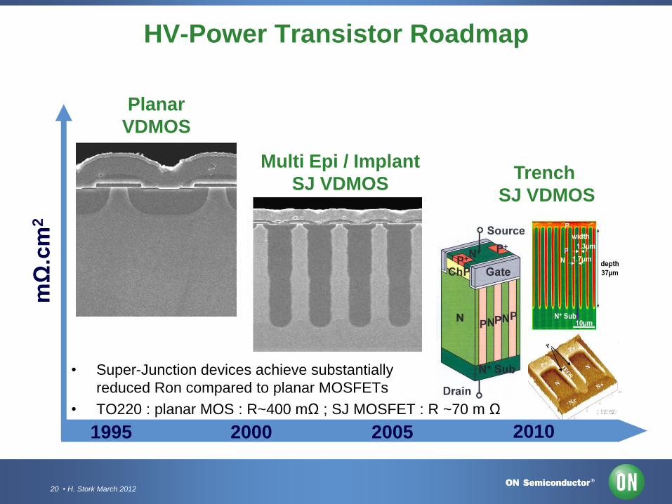
20 • H. Stork March 2012
HV-Power Transistor Roadmap m
Ω.c
m2
Multi Epi / Implant
SJ VDMOS
1995 2000 20102005
Planar
VDMOS
Trench
SJ VDMOS
• Super-Junction devices achieve substantially
reduced Ron compared to planar MOSFETs
• TO220 : planar MOS : R~400 mΩ ; SJ MOSFET : R ~70 m Ω
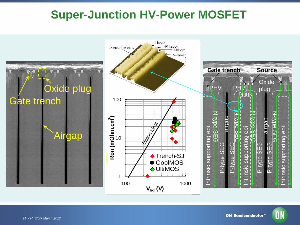
21 • H. Stork March 2012
Super-Junction HV-Power MOSFET
Gate trench
Oxide plug
Airgap
Gate trench
Oxide plug
Airgap
NlinkPHV PHV
N-ty
pe
SE
G
N-ty
pe
SE
G
N-ty
pe
SE
G
N-ty
pe
SE
G
P-t
yp
e S
EG
P-t
yp
e S
EG
P-t
yp
e S
EG
P-t
yp
e S
EG
Intr
insic
su
pp
ort
ing e
pi
Intr
insic
su
pp
ort
ing e
pi
airg
ap
airg
ap
Oxide
plug
SourceGate trench
Intr
insic
su
pp
ort
ing e
pi
NlinkPHV PHV
N-ty
pe
SE
G
N-ty
pe
SE
G
N-ty
pe
SE
G
N-ty
pe
SE
G
P-t
yp
e S
EG
P-t
yp
e S
EG
P-t
yp
e S
EG
P-t
yp
e S
EG
Intr
insic
su
pp
ort
ing e
pi
Intr
insic
su
pp
ort
ing e
pi
airg
ap
airg
ap
Oxide
plug
SourceGate trench
Intr
insic
su
pp
ort
ing e
pi
1
10
100
100 1000Vbd (V)
Ro
n (
mO
hm
.cm
2)
Trench-SJCoolMOSUltiMOS
15
20
25
30
35
600 650 700 750Vbd (V)
Ro
n (
mO
hm
.cm
2)
Comp4, Trench
Comp1, ME/MI
Comp2, ME/MI
Comp3, ME/MI
This work

22 • H. Stork March 2012
IGBT & MOSFET Structures
n- Epi
p ch
n+ Sub
n- Epi
PHV ch
n buffer
p+ Sub
P
N
P
Gate
Collector
Emitter
PNP
Top
Metal
IGBT MOSFET
FieldStop
n+
Source
Drain

23 • H. Stork March 2012
IGBT PT & NPT Structures
FZ-subn- Epi
PHV ch
n buffer
p+ Sub
P
N
P
Gate
Collector
Emitter
PNP
Top
Metal
PT IGBT NPT IGBT
FieldStop
Punch Through (PT) is used to
describe p+ sub/buffer/epi structure.
Non-Punch Through (NPT) is non-epi
structure depending on thin wafer process.
p+ Implant

24 • H. Stork March 2012
Planar & Trench MOSFET Structure
In the trench structure the channel is formed on the sides of trenches dug
vertically into the silicon.
Current flow is strictly vertical. There is no “pinch” region. This means the
trenches and source openings may be arbitrarily small. Channel density is very
large.
Conduction is still majority carrier, all electrons in this case. Switching is faster.
n- Epi
PHV ch
p+ Sub
P
N
P
n- Epi
PHV ch
n+ Sub
P
N
P
PHV chP PHV chP
Top Metal
n+ Sub
n+
Top Metal
n- Epi
PHV
Back MetalBack Metal

25 • H. Stork March 2012
Process Challenges
Back side implantation:- P-type dopant for NPT IGBT
- P-type and N-type for FS IGBT
- Handling of thin wafers
Wafer thinning:- Conventional / TAIKO
- Minimize thickness variation
- Thinning down to 70um (600V) or
40um (400V)
- Subsequent handling of thin wafers
for back side implantation, cleaning,
annealing, metallization, shipping,
probe, die singulation, assembly
- Wafer support systems are
expensive, need substantial
floorspace and the use of adhesives
is limited to low temperatures.
Trench module:- Trench etch: good uniformity
and high etch rate for good
yield and high throughput
- Gate oxide: low defectivity
Back side annealing:-Conventional / laser
- Electrical performance / costs
Back side lithography-Needed for an integrated diode
- Additional handling of thin wafers
Substrate:- FZ-Si or denuded Cz-Si
- Good uniformity of electrical resistivity
- Low oxygen content – no precipitates

26 • H. Stork March 2012
Die Thickness Reduction
50µm with Backmetal
1990 2000 20152010
50µm
100µm
250µm
10µm
70µm
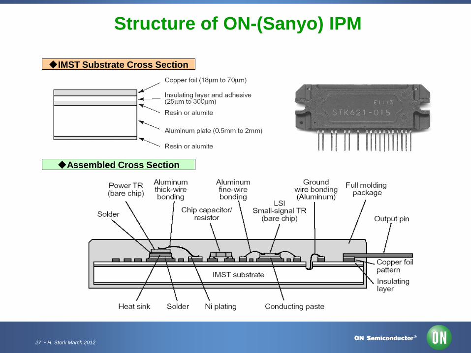
27 • H. Stork March 2012
◆IMST Substrate Cross Section
◆Assembled Cross Section
Structure of ON-(Sanyo) IPM

28 • H. Stork March 2012
Inverter control
Damper control
Energy Saving effect
Air Flow((%)
Power Requirements(%)
Damper (Valve) Control Commercial Power(15kW x 91% x 2,000h) +(15kW x 76% x 2,000h)
85% Air flow 60% Air flow
= 50,100kWh
Inverter Control Commercial Power
(15kW x 66% x 2,000h) +(15kW x 25% x 2,000h)85% Air flow 60% Air flow
= 27,300kWh
Annual Energy Saving50,100kWh-27,300kWh = 22,800kWh/year
Comparison of energy saving: Damper control vs. Inverter control
Energy-Saving Effect: Power Charges as 16 yen/kWh
22,800kWh x 0.195 $ = 4,451 $/ year
Amortize equipment period of 450,000 yen Inverter
5488 $ / 4,451yen = 1.2 years
Annual CO2 Reduction
CO2 emission coefficient: 0.12kg/kWh*
22,800kWh x 0.12kg/kWh = 2,736kg/year* Source: Global Environment Bureau Ministry of the Environment
Energy Efficiency using Inverter
5

29 • H. Stork March 2012
Trends in Power Devices: Si, GaN, and SiC
IGBT
SJ-HVFET
GaN
HEMT

30 • H. Stork March 2012
AlGaN/GaN HEMT: Why GaN ?
Noise Figure (NF)- Less Carrier Scattering
- Small RF Loss
Maximum Oscillation
Frequency (fmax)- High Saturation Velocity
- Small Parasitic Capacitance
Maximum Drain
Current (Imax)- High Carrier Density
- High Electron Mobility
Maximum Breakdown
Field (BVDmax)- High Carrier Density
- High Electron Mobility
Maximum Operating
Temperature (Tjmax)- Wide Bandgap
- High Potential Barrier
(A/mm) (dB)
(V/um)
(Deg C)
(GHz)
400
300
200
100
0

31 • H. Stork March 2012
• The varieties in power semiconductor Discrete and IC technologies
lead to a broad range in power package technologies
• Key power packaging advancements:
Die thickness reduction, thin wafers below 50µm including back metal
Wafer-level technologies, i.e. thick plated Cu or Au power metal
Advanced bonding technologies, i.e. thick Au, Al, Cu wire bonding, ribbon/clip bonding, power CSP
High power density handling capabilities and efficient heat sinking
High operating temperature up to 200C
Volumetric scaling leading to smaller package footprint and ultra-flat packages
Increased system integration through Power SIP technologies
2D Planar co-integration of a number of die and passive components
3D Vertical stacking technologies of wafer, die and package
Power Package Technologies

32 • H. Stork March 2012
Summary Comments
• Semiconductors are key to improve overall efficiency of the Electrical Energy Supply Chain by >25%
• The Power Semiconductor market is very diversified:A broad portfolio of semiconductor materials and devices are available or under development, dependent on power-rating (10 V.A – 10M V.A), frequencies, robustness, cost, …
• Many innovations are hitting the market in Si based MOSFET: SuperJunctions (HV), Vertical Field-plates (MV), Trench-LDMOS (LV), … pushing Si performance to new limits.
• Over the next decade, WBG-materials and devices, such as AlGaN-on-Si HEMT, will be increasingly popular because of superior performance. Cost will have to come down for widespread introduction.