Embed Size (px)
Citation preview

Conference Paper NREL/CP-540-46417 June 2010
Sensitivity of Solder Joint Fatigue to Sources of Variation in Advanced Vehicular Power Electronics Cooling A. Vlahinos Advanced Engineering Solutions M. O’Keefe National Renewable Energy Laboratory Presented at the 2009 ASME International Mechanical Engineering Conference and Exposition Lake Buena Vista, Florida November 13−19, 2009
NOTICE
The submitted manuscript has been offered by an employee of the Alliance for Sustainable Energy, LLC (ASE), a contractor of the US Government under Contract No. DE-AC36-08-GO28308. Accordingly, the US Government and ASE retain a nonexclusive royalty-free license to publish or reproduce the published form of this contribution, or allow others to do so, for US Government purposes.
This report was prepared as an account of work sponsored by an agency of the United States government. Neither the United States government nor any agency thereof, nor any of their employees, makes any warranty, express or implied, or assumes any legal liability or responsibility for the accuracy, completeness, or usefulness of any information, apparatus, product, or process disclosed, or represents that its use would not infringe privately owned rights. Reference herein to any specific commercial product, process, or service by trade name, trademark, manufacturer, or otherwise does not necessarily constitute or imply its endorsement, recommendation, or favoring by the United States government or any agency thereof. The views and opinions of authors expressed herein do not necessarily state or reflect those of the United States government or any agency thereof.
Available electronically at http://www.osti.gov/bridge
Available for a processing fee to U.S. Department of Energy and its contractors, in paper, from:
U.S. Department of Energy Office of Scientific and Technical Information P.O. Box 62 Oak Ridge, TN 37831-0062 phone: 865.576.8401 fax: 865.576.5728 email: mailto:[email protected]
Available for sale to the public, in paper, from: U.S. Department of Commerce National Technical Information Service 5285 Port Royal Road Springfield, VA 22161 phone: 800.553.6847 fax: 703.605.6900 email: [email protected] online ordering: http://www.ntis.gov/ordering.htm
Printed on paper containing at least 50% wastepaper, including 20% postconsumer waste

1
Sensitivity of Solder Joint Fatigue to Sources of Variation in Advanced Vehicular Power Electronics Cooling*
Andreas Vlahinos Advanced Engineering Solutions
Castle Rock, Colorado, USA
Michael O’Keefe National Renewable Energy Laboratory
Golden, Colorado, USA
ABSTRACT
This paper demonstrates a methodology for taking variation into account in thermal and fatigue analyses of the die attach for an inverter of an electric traction drive vehicle. This method can be used to understand how variation and mission profile affect parameters of interest in a design. Three parameters are varied to represent manufacturing, material, and loading variation: solder joint voiding, aluminum nitride substrate thermal conductivity, and heat generation at the integrated gate bipolar transistor, or IGBT. The influence of these parameters on temperature and solder fatigue life is presented. The heat generation loading variation shows the largest influence on the results for the assumptions used in this problem setup.
INTRODUCTION Power inverters are key components of the electric traction
drives of hybrid electric, plug-in hybrid electric, fuel cell electric, and pure electric vehicles [1, 2]. Research and development of power inverters is currently focused on reducing the cost, weight, and volume of the technology while maintaining and/or increasing reliability [1, 2]. If the research goals related to cost, weight, volume, and reliability can be met, more advanced vehicles can enter the marketplace and reduce the amount of petroleum required for transportation.
Current-generation inverter designs used in today’s hybrid vehicles are built on proven technology that has demonstrated high reliability. In contrast, the next generation of inverter concepts combines new materials, new heat transfer methods, and new packaging concepts under increased loads and in smaller spaces. Furthermore, there is interest in expanding the range of temperatures and stresses under which these technologies can operate [3, 4]. For these new technologies and conditions, reliability is, as yet, unproven.
In a production environment, reliability data can be obtained from statistical measures of empirical data or from product testing. However, design changes during production to fix reliability problems are quite expensive. In contrast, during the early phases of research, design changes are cheap to make. However, prototypes may not even be available. Therefore, at the very earliest stages of design, other methods must be used to estimate reliability (see page 3 of [5] for further discussion).
One such method is physical simulation, which we employ here.
Die attach failure has been reported as a critical failure mechanism in power electronics packages and will be the focus of this paper [5, 6]. Die solder joint fatigue is one form of die debonding failure. De-adhesion of the die is another major die debonding failure mechanism [5]. De-adhesion is mainly due to manufacturing defects such as excessive solder voiding or poor wetting of the solder [5]. In this study, we assume that the manufacturing quality is sufficient to avoid failure via de-adhesion. Die attach fatigue results in cracking, which eventually causes the thermal resistance of the joint to increase. Thus, failure of the die attach solder typically results in failure of the power semiconductor due to exceeding the device’s thermal limits [6].
In this paper, we explore the sensitivity of die attach solder joint fatigue to sources of variation for a baseline liquid-cooled power inverter (with pin-fin heat exchanger) placed in a high-temperature automotive environment. Sources of variation can come from the manufacturing process (variation in package geometry and/or some initial voiding during solder joint creation), the material properties, and the loading (coolant temperatures, flow rates, and heat inputs) [2]. Variations and uncertainty associated with these physical parameters exhibit probabilistic distributions (probability density functions). Therefore, the fatigue life (an output) will also exhibit a probability density function.
The modeling technique demonstrated here provides a framework for evaluating the effect of variation on solder joint fatigue prediction. Solder joint fatigue failure was chosen to study because it is an important failure mode for modern day automotive power inverters [5, 6]. *This paper was originally presented at the 2009 ASME International Mechanical Engineering Conference & Exposition, November 13-19, 2009, Lake Buena Vista, Florida (paper no. IMECE2009-11443).

2
There are numerous studies on solder joint reliability in the context of electronics packaging (see, for example, [7-11]). Analytical models have been proposed to estimate the thermally induced (elastic) stresses due to differences in coefficients of thermal expansion between adjacent layers in multilayered bonded materials (see, for example, [12-13]). In these studies, both experimental and analytical evidence indicates that stresses in “soft” lead-based soldered joints (similar to what is used in our analysis) are highest at the edges.
Reference [6] applies the finite element method to explore the failure of solder joints in power electronics packages. The authors use Anand’s viscoplastic model, which incorporates both plasticity and creep phenomena to describe the behavior of the solder joint. The authors are able to show that thermal cycling has a significant effect on solder joint reliability and recommend connecting the finite element model with a damage mechanics constitutive model to predict the number of cycles to failure.
In reference [2], the authors apply a suite of computer-aided engineering tools, including finite element analysis, to study two reliability issues in power electronics modules: wire bond liftoff and substrate fracturing. The combined effects of process and material uncertainty on reliability are highlighted as concerns. The authors state that if a physics-of-failure model were available, an assessment of cycles to failure could be made.
MODEL DESCRIPTION The physical model that we created for this study is
presented in this section. We used a commercially available finite element code for simulation. We varied three parameters in this study: the heat generated from the IGBT (a variation in loading), the thermal conductivity of the IGBT solder joint (assumed to be due to the initial presence of voids), and the thermal conductivity of the substrate (a variation in material properties). These three properties were chosen to demonstrate the process of applying robust design techniques to the domain of power module thermal stress and reliability simulation. In truth, any parameter that can be modeled could have been chosen.
Model Overview For this analysis, we considered a standard inverter design
with a basic geometry similar to that of commercially available designs. The emphasis of this study is on demonstrating the analytical approach, although we will also point out some general insights that can be gained from the analytical results.
As an example to give the context of our model, Figure 1 shows the power inverter from a popular hybrid electric vehicle. The left-hand side of the inverter (circled by a dashed line) is used to power the main traction motor of the vehicle and will be the focus of our subsequent discussion. The traction motor inverter consists of 12 IGBTs and 12 diodes, and each pair of two IGBTs and two diodes (i.e., four devices) forms an electrical switch (each pair is electrically in parallel to reduce the amount of current any one device is exposed to). Electrical
current is routed across the inverter through the metallization on the surface of the inverter and through wire bonds. Wire bonds are also used to deliver current from the gate driver (not shown) to the individual IGBTs to turn them on and off. A more extensive discussion of this inverter topology can be found in [14].
Our physical model is shown in Figures 2 and 3. The model represents a subset of the full vehicle inverter. We assume that the boundary conditions on the model correspond to the last device cooled along the cooling channel; this device typically experiences the hottest temperatures. Our model consists of one IGBT and diode pair and the layers of the inverter package between the devices and the cooling system. The model is simplified to show only the relevant geometry. For example, wire bonds are not explicitly modeled.
It will be important in our model to get a correct prediction of heat transfer and temperatures because the stresses that cause fatigue in the solder joint are thermally induced due to differences in the coefficient of thermal expansion. For this reason, we will briefly discuss the thermal boundary conditions and relevant material properties before focusing on the interaction of model variation and fatigue results.
Figure 1. Example of Hybrid Electric Vehicle Inverter
Model Geometry The geometry used for the devices is similar in size, shape,
and layout to that of commercial hybrid inverters. In our design, we employ an elliptical pin-fin heat exchanger (see Figure 2). The large rectangular region on the top of the model is the IGBT. The smaller square device is a diode. Below the IGBT and diode is a direct bond copper (DBC) substrate consisting of a top copper metallization layer, a substrate layer of aluminum nitride (AlN), and a lower copper layer. The IGBT and diode are soldered to the DBC. In turn, the DBC is soldered to the next layer down, which is a base plate. The base plate is fixed to the heat sink via bolts (not shown) and contains a thermal interface material (TIM) to create good thermal contact. Note that newer designs integrate the base plate and heat sink into one solid item. The advantage of having a
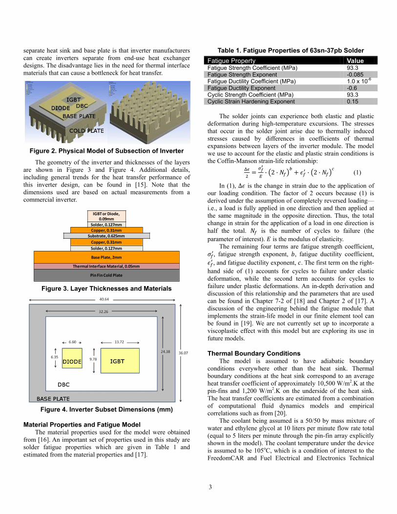
3
separate heat sink and base plate is that inverter manufacturers can create inverters separate from end-use heat exchanger designs. The disadvantage lies in the need for thermal interface materials that can cause a bottleneck for heat transfer.
Figure 2. Physical Model of Subsection of Inverter
The geometry of the inverter and thicknesses of the layers are shown in Figure 3 and Figure 4. Additional details, including general trends for the heat transfer performance of this inverter design, can be found in [15]. Note that the dimensions used are based on actual measurements from a commercial inverter.
Figure 3. Layer Thicknesses and Materials
Figure 4. Inverter Subset Dimensions (mm)
Material Properties and Fatigue Model The material properties used for the model were obtained
from [16]. An important set of properties used in this study are solder fatigue properties which are given in Table 1 and estimated from the material properties and [17].
Table 1. Fatigue Properties of 63sn-37pb Solder Fatigue Property Value Fatigue Strength Coefficient (MPa) 93.3
Fatigue Strength Exponent -0.085 Fatigue Ductility Coefficient (MPa) 1.0 x 10Fatigue Ductility Exponent
-6
-0.6 Cyclic Strength Coefficient (MPa) 93.3 Cyclic Strain Hardening Exponent 0.15
The solder joints can experience both elastic and plastic
deformation during high-temperature excursions. The stresses that occur in the solder joint arise due to thermally induced stresses caused by differences in coefficients of thermal expansions between layers of the inverter module. The model we use to account for the elastic and plastic strain conditions is the Coffin-Manson strain-life relationship:
(1)
In (1), is the change in strain due to the application of our loading condition. The factor of 2 occurs because (1) is derived under the assumption of completely reversed loading—i.e., a load is fully applied in one direction and then applied at the same magnitude in the opposite direction. Thus, the total change in strain for the application of a load in one direction is half the total. is the number of cycles to failure (the parameter of interest). is the modulus of elasticity.
The remaining four terms are fatigue strength coefficient, , fatigue strength exponent, , fatigue ductility coefficient, , and fatigue ductility exponent, . The first term on the right-
hand side of (1) accounts for cycles to failure under elastic deformation, while the second term accounts for cycles to failure under plastic deformations. An in-depth derivation and discussion of this relationship and the parameters that are used can be found in Chapter 7-2 of [18] and Chapter 2 of [17]. A discussion of the engineering behind the fatigue module that implements the strain-life model in our finite element tool can be found in [19]. We are not currently set up to incorporate a viscoplastic effect with this model but are exploring its use in future models.
Thermal Boundary Conditions The model is assumed to have adiabatic boundary
conditions everywhere other than the heat sink. Thermal boundary conditions at the heat sink correspond to an average heat transfer coefficient of approximately 10,500 W/m2.K at the pin-fins and 1,200 W/m2
The coolant being assumed is a 50/50 by mass mixture of water and ethylene glycol at 10 liters per minute flow rate total (equal to 5 liters per minute through the pin-fin array explicitly shown in the model). The coolant temperature under the device is assumed to be 105
.K on the underside of the heat sink. The heat transfer coefficients are estimated from a combination of computational fluid dynamics models and empirical correlations such as from [20].
oC, which is a condition of interest to the FreedomCAR and Fuel Electrical and Electronics Technical
IGBT or Diode, 0.09mm
Solder, 0.127mmCopper, 0.31mm
Substrate, 0.625mmCopper, 0.31mmSolder, 0.127mm
Base Plate, 2mm
Thermal Interface Material, 0.05mm
Pin Fin Cold Plate
4
Team. A discussion of the rationale and motivation for the FreedomCAR and Fuel Partnership, as well as the coolant temperature setting, can be found in [1].
Loading Cycle Heat generation in the IGBT and diodes of an inverter
during normal operation is due to a combination of on-state and switching losses. This heat is simulated in the model as a constant heat input at the IGBT and diodes, respectively. Heat is assumed to be transferred only through the heat sink. All other boundary conditions are assumed to be adiabatic. The inverter is typically packaged under the hood in a casing as part of a larger power module. A silicone gel is typically layered on the top of the inverter surface to protect it from direct exposure to the environment. Although heat may be conducted through the wire bonds themselves, we have taken the conservative assumption that no heat is transferred through the top of the inverter.
Although an automotive inverter is subjected to other loading conditions—most notably, vibrations and corrosive environments—we have chosen only one loading condition for consideration during this study.
The loading cycle used in this study is similar to power cycling. The simulation test is equivalent to heating the inverter under its own power to steady-state conditions and then allowing the inverter to cool back to the initial ambient condition. Note that we do not take transient phenomena such as creep into account during this process.
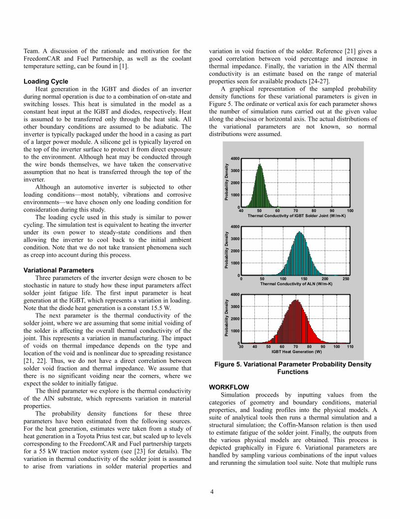
Variational Parameters Three parameters of the inverter design were chosen to be
stochastic in nature to study how these input parameters affect solder joint fatigue life. The first input parameter is heat generation at the IGBT, which represents a variation in loading. Note that the diode heat generation is a constant 15.5 W.
The next parameter is the thermal conductivity of the solder joint, where we are assuming that some initial voiding of the solder is affecting the overall thermal conductivity of the joint. This represents a variation in manufacturing. The impact of voids on thermal impedance depends on the type and location of the void and is nonlinear due to spreading resistance [21, 22]. Thus, we do not have a direct correlation between solder void fraction and thermal impedance. We assume that there is no significant voiding near the corners, where we expect the solder to initially fatigue.
The third parameter we explore is the thermal conductivity of the AlN substrate, which represents variation in material properties.
The probability density functions for these three parameters have been estimated from the following sources. For the heat generation, estimates were taken from a study of heat generation in a Toyota Prius test car, but scaled up to levels corresponding to the FreedomCAR and Fuel partnership targets for a 55 kW traction motor system (see [23] for details). The variation in thermal conductivity of the solder joint is assumed to arise from variations in solder material properties and
variation in void fraction of the solder. Reference [21] gives a good correlation between void percentage and increase in thermal impedance. Finally, the variation in the AlN thermal conductivity is an estimate based on the range of material properties seen for available products [24-27].
A graphical representation of the sampled probability density functions for these variational parameters is given in Figure 5. The ordinate or vertical axis for each parameter shows the number of simulation runs carried out at the given value along the abscissa or horizontal axis. The actual distributions of the variational parameters are not known, so normal distributions were assumed.
Figure 5. Variational Parameter Probability Density
Functions
WORKFLOW Simulation proceeds by inputting values from the
categories of geometry and boundary conditions, material properties, and loading profiles into the physical models. A suite of analytical tools then runs a thermal simulation and a structural simulation; the Coffin-Manson relation is then used to estimate fatigue of the solder joint. Finally, the outputs from the various physical models are obtained. This process is depicted graphically in Figure 6. Variational parameters are handled by sampling various combinations of the input values and rerunning the simulation tool suite. Note that multiple runs
40 50 60 70 80 90 1000
1000
2000
3000
4000
Thermal Conductivity of IGBT Solder Joint (W/m-K)
Pro
babi
lity
Dens
ity
0 50 100 150 200 2500
1000
2000
3000
4000
Thermal Conductivity of ALN (W/m-K)
Pro
babi
lity
Dens
ity
30 40 50 60 70 80 90 100 1100
1000
2000
3000
4000
IGBT Heat Generation (W)
Pro
babi
lity
Dens
ity

5
can be performed very quickly under conditions in which the input loading changes by some constant factor in comparison to a reference case. Under these circumstances, only the reference case needs to be fully run, and the results can be scaled to determine all other cases.
Figure 6. Simulation Workflow
The sampling of two variational parameters (AlN thermal conductivity and solder joint thermal conductivity) is depicted in Figure 8.
RESULTS The thermal and fatigue results are presented in the
sections that follow. In addition, we show how concepts from robust design could be applied to interpret the results.
Thermal Results Because the magnitude of the heat generated by the IGBT
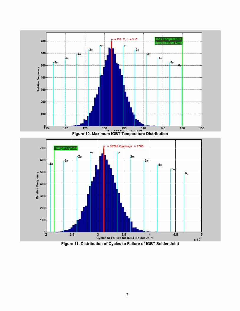
is higher than that of the diode, we see the highest temperatures consistently occurring on the IGBT device itself. Maximum temperature varies stochastically with the input variable distributions, and the IGBT heat rejection is the most significant. A snapshot of the temperature distribution across the model is given in Figure 7. The output distribution of maximum IGBT temperature is given in Figure 10. A maximum specification limit of 150o
C is assumed for the IGBT.
Figure 7. Temperature Distribution
(Tmax
= 138.8)
Figure 8. Sampling Variational Parameters
40 50 60 70 80 90 1000
100
200
300
400
500
600
Thermal Conductivity of IGBT Solder Joint (W/m-K)
40 50 60 70 80 90 10040
50
60
70
80
90
100
Thermal Conductivity of IGBT Solder Joint (W/m-K) The
rmal
Con
duct
ivity
of A
LN (W
/m-K
)
0 100 200 300 400 500 60030
40
50
60
70
80
90
100
The
rmal
Con
duct
ivity
of A
LN (W
/m-K
)
4060
80100
4060
80100
0
50
100
150
K of IGBT Solder Joint K of ALN
Q

6
Fatigue Results In this section, we look at the cycles to failure of the IGBT
solder joint. For a discussion of failure prediction for other solder joints in the package, see [28]. We define failure to represent the number of cycles until the onset of cracking in the solder joint. Upon onset of cracking, the device may survive additional cycles as the crack propagates and eventually causes the effective thermal conductivity to get so low that the device junction temperature goes above specification limits and/or the die becomes completely unattached.
The highest areas of stress occur at the edges and corners, resulting in cracks propagating from these locations. This can be seen in the plot of cycles to failure in Figure 9. This same phenomenon can be seen in the literature [29, 10] and can be explained through simple analytical models of stresses in epitaxial layered devices (see, for example, [12]).
Figure 9. Fatigue Life of IGBT Solder
Robust Design Investigation In this section, we show the output distributions that arise
from the stochastic inputs used (see Figure 5). In Figure 10, the distribution of maximum IGBT temperature is shown. As can be seen, the output distribution of maximum junction temperature is within an acceptable range for the problem setup chosen. The results are normally distributed, and the number of standard deviations away from the mean is plotted on the graphs.
A cycle life of 22,000 cycles was selected for a desired life of this product based on 4 cycles per day, 365 days per year, and a target 15-year life. Figure 11 shows the distribution of cycles to failure and indicates that the IGBT die attach, under the given conditions, would survive the 15-year life with >99% confidence.
The influence of the input parameters on the final results is presented in Figure 12 and Figure 13. The influence is calculated by normalizing the difference between the output result when the input parameter is high and when the input parameter is low. As can be seen, the thermal loading has the highest influence on both the solder joint reliability and the maximum package temperature, which indicates the importance of knowing the usage environment for reliability work.
CONCLUSIONS This paper presented a methodology for taking variable
input parameters into account during a solder die attach fatigue analysis for an automotive inverter of an electric traction drive vehicle. Since the inverter, its boundary conditions, and loading conditions were invented for the purpose of this analysis, we must be careful in drawing specific conclusions about overall inverter performance. Specifically, several failure mechanisms associated with an automotive inverter are not taken into account in the current study (for example, wire bond fatigue failure and substrate cracking). Furthermore, our failure physics model did not take viscoplastic effects such as creep into account.
For the conditions evaluated in this study, the thermal loading condition was shown to have the strongest effect on the output parameters of temperature and fatigue life. Although we did not look at an extensive list of variational parameters, the large impact that heat generation has on fatigue life highlights the importance of understanding the mission profile to which the inverter will be subjected.
Using the design process presented, we have shown that one may be able to estimate the fatigue life of a power inverter for automotive applications using commercially available software. This method allows the designer to understand how variation in input parameters and mission profile can affect metrics of interest, such as fatigue life.
Further work on transient heat generation should be conducted using vehicle systems tools to better estimate a loading profile in place of the simple loading cycle used in this study. Additional loads, such as vibrations, should also be taken into account along with a more comprehensive analysis of additional failure modes and mechanisms (such as wire bond flexural fatigue and substrate cracking). Validation testing will be critical to confirm model predictions. Once these additions are made to the scope of the problem, a meaningful robust design optimization can be attempted.
7
Figure 10. Maximum IGBT Temperature Distribution
Figure 11. Distribution of Cycles to Failure of IGBT Solder Joint
2 2.5 3 3.5 4 4.5 5x 10⁴
0
100
200
300
400
500
600
700 µ = 35708 Cycles, σ = 1705
σ-σ2σ-2σ
3σ-3σ 4σ-4σ
5σ 6σ
Target Cycles
Cycles to Failure for IGBT Solder Joint
Rel
ativ
e Fr
eque
ncy

8
Figure 12. Influence of Inputs on Maximum
Temperature
Figure 13. Influence of Inputs on IGBT Solder Fatigue
NOMENCLATURE IGBT integrated gate bipolar transistor
change in strain due to loading number of cycles to failure
modulus of elasticity (Young’s Modulus) fatigue strength coefficient
fatigue strength exponent fatigue ductility coefficient
fatigue ductility exponent PDF probability density function
ACKNOWLEDGMENTS We would like to acknowledge Susan Rogers of the U.S.
Department of Energy’s Vehicle Technologies Program for funding this effort.
REFERENCES [1] FreedomCAR & Fuels Electrical and Electronics
Technical Team. (November 2006). “Electrical and Electronics Technical Team Roadmap,” online at
http://www1.eere.energy.gov/vehiclesandfuels/pdfs/program/eett_roadmap.pdf
[2] C. Bailey, C., Tilford, T., and Lu, H., 2007, “Reliability Analysis for Power Electronics Modules,” presented at the 30th IEEE International Spring Seminar on Electronics Technology, Cluj-Napoca, Romania, May 9-13, 2007.
[3] McCluskey, F. P., 2007, Power Modulation Investigation for High Temperature (175oC–200 o
[4] Zhu, N., Van Wyk, J. D., and Liang, Z. X., 2004, “Thermal-Mechanical Stress Analysis in Embedded Power Modules,” IEEE Technical Paper, Presented at the 35
C) Automotive Applications, Oak Ridge National Laboratory Technical Report no. ORNL/TM-2007/046.
th
[5] McCluskey, F. P., 2006, “Power Module Reliability in High Temperature Applications: Interim Report on the Results of Phase I,” Dept. of Mechanical Engineering, University of Maryland, College Park, MD, Subcontractor Report submitted to Oak Ridge National Laboratory.
Annual IEEE Power Electronics Specialists Conference in Aachen, Germany, pp. 4503-4508.
[6] Ye, H., Lin, M., and Basaran C., 2002, “Failure Modes and FEM Analysis of Power Electronic Packaging,” Finite Elements in Analysis and Design, vol. 38, 2002, pp. 601-612.
[7] Frear, D. , Grivas, D., and Morris, J.W., Jr., “Parameters Affecting Thermal Fatigue Behavior of 60Sn-40Pb Solder Joints,” Journal of Electronic Materials, vol. 18, no. 6, 1989, pp. 671-680.
[8] Shaw, M.C., 2003, “High-Performance Packaging of Power Electronics,” MRS Bulletin, vol. 28, no. 1, pp. 41-50.
[9] He, J., Shaw, M.C., Mather, J.C., and Addison, R.C., Jr., 1998, “Direct Measurement and Analysis of the Time-Dependent Evolution of Stress in Silicon Devices and Solder Interconnections in Power Assemblies,” 33rd IAS Annual Meeting, IEEE Industry Applications Conference, St. Louis, MO.
[10] Shaw, M. C., He, J., Mather, J. C., and Addison, R. C. Jr., 2000, “Effects of Plasticity on Reliability in Multilayered Electronic Packages,” IEEE technical paper presented at the 2000 Inter-Society Conference on Thermal Phenomena, pp. 279-286.
[11] Stinson-Bagby, K., Huff, D., Katsis, D., Van Wyk, D., and Lu, G.Q., 2004, “Thermal Performance and Microstructures of Lead versus Lead-Free Solder Die Attach Interface in Power Device Packages,” presented at the 2003 International Symposium on Microelectronics, pp. 27-32.
[12] Suhir, E., 1986, “Stresses in Bi-Metal Thermostats,” Journal of Applied Mechanics, vol. 53, pp. 657-660.
[13] Ru, C., 2002, “Interfacial Thermal Stresses in Bimaterial Elastic Beams: Modified Beam Models Revisited,” Journal of Electronic Packaging, vol. 124, pp. 141-146.
[14] Staunton, R. H., Ayers, C. W., Marlino, L. D., Chiasson, J. N., and Burress, T. A., May 2006, Evaluation of 2004 Toyota Prius Hybrid Electric Drive System, Oak Ridge National Laboratory Technical Report, ORNL/TM-2006/423.
[15] O’Keefe, M., and Bennion, K., 2007, “A Comparison of Hybrid Electric Vehicle Power Electronics Cooling Options,”

9
presented at the 3rd
[16] Lau, J. H., and Pao, Y. H., 1997, Solder Joint Reliability of BGA, CSP, Flip Chip, and Fine Pitch SMT Assemblies, McGraw Hill, New York.
Annual IEEE Vehicle Power and Propulsion Systems Conference. Arlington, TX, September 9-12, 2007, pp. 116-123.
[17] Bannantine, J. A., Comer, J. J., and Handrock, J. L., 1990, Fundamentals of Metal Fatigue Analysis, Prentice-Hall, New York.
[18] Shigley, J. E., and Mischke, C. R., 1989, Mechanical Engineering Design, 5th
[19] Hancq, D., Walters, A., and Beuth, J., 2000, “Development of an Object-Oriented Fatigue Tool,” Engineering with Computers, vol. 16, pp. 131-144.
Edition, McGraw-Hill, Inc., New York, pp. 272-273.
[20] Montelpare, S., and Ricci, R., 2004, “An Experimental Method for Evaluating the Heat Transfer Coefficient of Liquid-Cooled Short Pin-Fins Using Infrared Thermography,” Experimental Thermal and Fluid Science, vol. 28, pp. 815-824.
[21] Zhu, N., 1999, “Thermal Impact of Solder Voids in the Electronic Packaging of Power Devices,” Proceedings of the 15th
[22] Biswal, L., Krishna, A., and Sprunger, D., 2005, “Effects of Solder Voids on Thermal Performance of a High Power Electronic Module,” Proceedings of the 7
IEEE SemiTherm Symposium, pp. 22-29.
th
[23] O’Keefe, M., Bennion, K., and Albright, G., 2007, HEV Inverter Thermal Duty Cycles, National Renewable Energy Laboratory Report No. MP-540-41801, Golden, CO.
Electronics Packaging Technology Conference, vol. 2, pp. 526-531.
[24] Material Properties for Aluminum Nitride from Accuratus, online at http://www.accuratus.com/alumni.html.
[25] NTK Spark Plug Co., Ltd., 2002, “Aluminum Nitride (AlN) Ceramic Package/Substrate,” online presentation, http://www.ntktech.com/AlN/ALN%20for%20web.pdf.
[26] Franco Júnior, A., and Shanafield, D. J., 2004, “Thermal Conductivity of Polycrystalline Aluminum Nitride (AlN) Ceramics,” Cerâmica, vol. 50, no. 315, pp. 247-253, São Paulo, Brazil, July 2004.
[27] Savrun, E., and Nguyen, V., 2006, “High Thermal Conductivity Aluminum Nitride for High Power Microwave Windows—An Update,” Sienna Technologies white paper, online at http://www.siennatech.com/HIGH%20THERMAL%20CO%C9AVE%20WINDOWS.pdf
[28] O’Keefe, M., and Vlahinos, A., 2009, “Impacts of Cooling Technology on Solder Fatigue for Power Modules in Electric Traction Drive Vehicles,” presented at the 2009 Vehicle Power and Propulsion Systems Conference, Dearborn, MI, September 7-11, 2009.
[29] He, J., Shaw, M. C., Mather, J. C., and Addison, R. C. Jr., 1998, “Direct Measurement and Analysis of the Time-Dependent Evolution of Stress in Silicon Devices and Solder Interconnections in Power Assemblies,” Proceedings of the 33rd IAS Annual Meeting, 1998 IEEE Industry Applications Conference, St. Louis, MO, vol. 2, pp. 1038-1045.

F1147-E(10/2008)
REPORT DOCUMENTATION PAGE Form Approved OMB No. 0704-0188
The public reporting burden for this collection of information is estimated to average 1 hour per response, including the time for reviewing instructions, searching existing data sources, gathering and maintaining the data needed, and completing and reviewing the collection of information. Send comments regarding this burden estimate or any other aspect of this collection of information, including suggestions for reducing the burden, to Department of Defense, Executive Services and Communications Directorate (0704-0188). Respondents should be aware that notwithstanding any other provision of law, no person shall be subject to any penalty for failing to comply with a collection of information if it does not display a currently valid OMB control number. PLEASE DO NOT RETURN YOUR FORM TO THE ABOVE ORGANIZATION. 1. REPORT DATE (DD-MM-YYYY)
June 2010 2. REPORT TYPE
Conference Paper 3. DATES COVERED (From - To)
4. TITLE AND SUBTITLE
Sensitivity of Solder Joint Fatigue to Sources of Variation in Advanced Vehicular Power Electronics Cooling
5a. CONTRACT NUMBER DE-AC36-08-GO28308
5b. GRANT NUMBER
5c. PROGRAM ELEMENT NUMBER
6. AUTHOR(S) A. Vlahinos, Advanced Engineering Solutions Michael O'Keefe, NREL
5d. PROJECT NUMBER NREL/CP-540-46417
5e. TASK NUMBER FC08.7000
5f. WORK UNIT NUMBER
7. PERFORMING ORGANIZATION NAME(S) AND ADDRESS(ES) National Renewable Energy Laboratory 1617 Cole Blvd. Golden, CO 80401-3393
8. PERFORMING ORGANIZATION REPORT NUMBER NREL/CP-540-46417
9. SPONSORING/MONITORING AGENCY NAME(S) AND ADDRESS(ES)
10. SPONSOR/MONITOR'S ACRONYM(S) NREL
11. SPONSORING/MONITORING AGENCY REPORT NUMBER
12. DISTRIBUTION AVAILABILITY STATEMENT National Technical Information Service U.S. Department of Commerce 5285 Port Royal Road Springfield, VA 22161
13. SUPPLEMENTARY NOTES
14. ABSTRACT (Maximum 200 Words) This paper demonstrates a methodology for taking variation into account in thermal and fatigue analyses of the die attach for an inverter of an electric traction drive vehicle. This method can be used to understand how variation and mission profile affect parameters of interest in a design. Three parameters are varied to represent manufacturing, material, and loading variation: solder joint voiding, aluminum nitride substrate thermal conductivity, and heat generation at the integrated gate bipolar transistor. The influence of these parameters on temperature and solder fatigue life is presented. The heat generation loading variation shows the largest influence on the results for the assumptions used in this problem setup.
15. SUBJECT TERMS power electronics; power electronics cooling; solder joint fatigue analysis
16. SECURITY CLASSIFICATION OF: 17. LIMITATION OF ABSTRACT
UL
18. NUMBER OF PAGES
19a. NAME OF RESPONSIBLE PERSON a. REPORT
Unclassified b. ABSTRACT Unclassified
c. THIS PAGE Unclassified 19b. TELEPHONE NUMBER (Include area code)
Standard Form 298 (Rev. 8/98) Prescribed by ANSI Std. Z39.18