Embed Size (px)
Citation preview

DEVELOPMENT OF A LARGE-FORMAT SCIENCE-GRADE CMOS ACTIVE PIXELSENSOR FOR EXTREME ULTRA VIOLET SPECTROSCOPY AND IMAGING IN
SPACE SCIENCE
N.R. Waltham a, M. Prydderch a, H. Mapson-Menard a, Q. Morrissey a, R. Turchetta a,P. Pool b A. Harris b
a Rutherford Appleton Laboratory, Chilton, Didcot, Oxfordshire, UK, OX11 0QX;b e2v technologies, 106 Waterhouse Lane, Chelmsford, Essex, UK CM1 2QU.
ABSTRACT
We describe our programme to develop a large-format science-gradeCMOS active pixel sensor for future space science missions, and inparticular an extreme ultra-violet spectrograph for solar physics studies onESA’s Solar Orbiter. Our route to EUV sensitivity relies on adapting theback-thinning and rear-illumination techniques first developed for CCDsensors. So far we have designed and tested a 4k x 3k 5µm pixel sensorfabricated on a 0.25 µm CMOS imager process. Wafer samples of thesesensors have been thinned by e2v technologies with the aim of obtaininggood sensitivity at EUV wavelengths. We present our results to date, andplans for a new sensor of 2k x 2k 10 µm pixels to be fabricated on a 0.35µm CMOS process.
1 - INTRODUCTION
We are developing science-grade CMOS active pixel sensors for future space science missions.CMOS sensors promise significant advantages over today’s CCD technology. Firstly, modernCMOS processing enables smaller pixels than current science-grade CCDs, enabling more compactand lower mass instruments. Secondly, on-chip integration of the readout electronics minimizes thesize, mass and power requirements for ancillary control electronics and the associated problems ofspace-flight component procurement and radiation tolerance. Finally, deep sub-micron CMOStechnology promises significantly higher radiation tolerance in the space environment compared toCCDs.
Our goal is the development of a large-format CMOS sensor with useful sensitivity in the extremeultra-violet (EUV) for solar spectroscopy and imaging on ESA’s Solar Orbiter. Our route to EUVsensitivity relies in adapting the back-thinning and rear-illumination techniques first developed forCCD sensors.
We have developed a 4k x 3k pixel sensor with 5µm pixels fabricated on a 0.25 µm CMOS imagerprocess. Wafer samples of these sensors have been thinned by e2v technologies with the aim ofobtaining good sensitivity at EUV wavelengths. We present our results to date from both front- andback-illuminated versions of the sensor.
We also present our plans to develop a new EUV-sensitive sensor of 2k x 2k 10 µm pixels for theExtreme Ultra-violet Spectrograph (EUS) on ESA’s Solar Orbiter. In progress towards this goal, wehave designed a test-structure consisting of six arrays of 512 x 512 10 µm pixels. Each of the arrays

Report Documentation Page Form ApprovedOMB No. 0704-0188
Public reporting burden for the collection of information is estimated to average 1 hour per response, including the time for reviewing instructions, searching existing data sources, gathering andmaintaining the data needed, and completing and reviewing the collection of information. Send comments regarding this burden estimate or any other aspect of this collection of information,including suggestions for reducing this burden, to Washington Headquarters Services, Directorate for Information Operations and Reports, 1215 Jefferson Davis Highway, Suite 1204, ArlingtonVA 22202-4302. Respondents should be aware that notwithstanding any other provision of law, no person shall be subject to a penalty for failing to comply with a collection of information if itdoes not display a currently valid OMB control number.
1. REPORT DATE 13 JUL 2005
2. REPORT TYPE N/A
3. DATES COVERED -
4. TITLE AND SUBTITLE Development Of A Large-Format Science-Grade Cmos Active PixelSensor For Extreme Ultra Violet Spectroscopy And Imaging In Space Science
5a. CONTRACT NUMBER
5b. GRANT NUMBER
5c. PROGRAM ELEMENT NUMBER
6. AUTHOR(S) 5d. PROJECT NUMBER
5e. TASK NUMBER
5f. WORK UNIT NUMBER
7. PERFORMING ORGANIZATION NAME(S) AND ADDRESS(ES) Rutherford Appleton Laboratory, Chilton, Didcot, Oxfordshire, UK,OX11 0QX
8. PERFORMING ORGANIZATIONREPORT NUMBER
9. SPONSORING/MONITORING AGENCY NAME(S) AND ADDRESS(ES) 10. SPONSOR/MONITOR’S ACRONYM(S)
11. SPONSOR/MONITOR’S REPORT NUMBER(S)
12. DISTRIBUTION/AVAILABILITY STATEMENT Approved for public release, distribution unlimited
13. SUPPLEMENTARY NOTES See also ADM001791, Potentially Disruptive Technologies and Their Impact in Space Programs Held inMarseille, France on 4-6 July 2005., The original document contains color images.
14. ABSTRACT
15. SUBJECT TERMS
16. SECURITY CLASSIFICATION OF: 17. LIMITATION OF ABSTRACT
UU
18. NUMBEROF PAGES
12
19a. NAME OFRESPONSIBLE PERSON
a. REPORT unclassified
b. ABSTRACT unclassified
c. THIS PAGE unclassified
Standard Form 298 (Rev. 8-98) Prescribed by ANSI Std Z39-18

has been given a different pixel design to allow verification of our models, and our progresstowards optimizing a design for minimal system readout noise and maximum dynamic range. Thesesensors will also be back-thinned for characterization at EUV wavelengths.
2 - THE 4K X 3K PIXEL CMOS ACTIVE PIXEL SENSOR
A block diagram of the sensor and a schematic of the pixel are shown in Figure 1.
Many CMOS sensors, including our earlier designs [1], employ a simple 3-transistor pixel. Thisconsists of a Reset transistor for recharging the photodiode, a Source Follower for readout, and aRow Select transistor for connecting to the Column Read Lines. Apart from the fixed pattern noisedue to processing variations in the diodes and transistors of each pixel, the drawback to this designis that the Reset transistor generates kTC noise when it is switched off, and this can be the dominantnoise source in CMOS sensors. For our new sensor, we added a Transfer transistor to allowcorrelated double sampling of the reset charge and subsequently the integrated photon signalcharge, the aim being to cancel the kTC noise.
The transistors inside the pixel are usually all NMOS type, but if an NMOS Transfer transistor isused, the reset voltage to the pixel must be lowered to allow the gate to operate. This not only limitsthe voltage swing and hence the dynamic range of the pixel, but it also shifts the operating voltageaway from the positive power rail. This combines with the level shift imposed by the NMOS outputSource-Follower to compress the maximum linear signal range. We therefore decided to implementa PMOS Transfer transistor instead. In this case, the Reset transistor should also be implemented inPMOS to allow the photodiode to be reset to the positive power supply rail. However, we wereunable to accommodate this within our 5 µm x 5 µm pixel layout and thus had to compromise withthe PMOS Transfer transistor and NMOS Reset transistor.
Figure 1 - 4k x 3k pixel sensor architecture and pixel design
The sensor consists of 2880 rows, each of 4096 pixels, and is read out row by row under the controlof the Row Shift Register. Each pixel within a row is connected to a Column Read Line so that allpixels within a selected row are read in parallel. Each Column Read Line is connected to a pair of 1pF correlated double sampling (CDS) capacitors at the bottom of the array which provide storagefor samples of the pixel’s reset charge and integrated photon charge. Two 4096:1 multiplexersaddressed by a shift register route the sample pairs through to a differential switched-capacitoramplifier. This subtracts the two samples to generate a differential analogue output signal. Theamplifier’s gain can be programmed to be x1 or x2. We use a 14 bit differential-input analogue-to-digital converter to digitize the pixel signals at up to 1 Mpixels/s. The readout rate is limitedbecause of the inherently large resistances and parasitic capacitances of the 4096:1 multiplexersprolonging signal settling time to ~ 1 µs for 12 bits precision. This makes the readout time for thewhole sensor ~ 12 seconds, which means cooling is required to reduce the leakage current.
RowSelect
Reset
Photodiode
Reset Voltage
Vdd
SourceFollower
ColumnRead Line
Transfer
ParasiticCapacitor
Shift Register
CDS Capacitors
4k:1 Multiplexers Amp
PixelArray
RowShiftRegister
DifferentialAnalogueOutput

The sensor was fabricated on a 0.25 µm CMOS process intended for imaging chips, and featuringan 8 µm epitaxial layer. The foundry has developed an optimized version of the N-well/P-epi diodewith a dark current of 28 mV/second for a 1.9 µm2 photodiode. The thresholds for the Reset, RowSelect and Source-Follower transistors have also been optimized individually. The pixel array andthe analogue readout circuits are powered from 3.3 V, while the logic is powered from 2.5 V. All ofthe sensor’s control clocks and digital interface signals are buffered with on-chip LVDStransmitters and receivers.
Each sensor is mounted on an invar block and wire-bonded to a small printed circuit board (PCB)that carries ceramic decoupling capacitors for the power and DC bias supplies, and terminationresistors for the LVDS clock receivers. A 51-way micro-D connector soldered to the underside ofthe PCB provides the connections interface. A black-anodised aluminium cover provides protectionfor the bond wires and a small degree of optical shielding over the sensor’s readout circuitryrunning along the long edge of the chip. Photographs of the sensor, PCB and bond-wire cover arereproduced in Figure 2.
Figure 2 - Photograpghs of the 4k x 3k pixel sensor
3 - BACK-THINNING FOR EUV SENSITIVITY
Figure 3 shows the optical absorption coefficient in silicon over the EUV-Visible band. At EUVwavelengths the absorption depth is so shallow that the oxide layers on front-illuminated CMOSsensors absorb the photons before they reach the photodiodes. Our route to EUV sensitivity relies inadapting the back-thinning and rear-illumination techniques first developed for CCD sensors.

Figure 3 - Optical absorption coefficient in silicon
Figure 4 illustrates a cross-section through a typical front-illuminated CMOS sensor, and then afterback-thinning. After first bonding the front side of the sensor to another substrate to providemechanical support, the bulk silicon is removed by chemical etch. For CMOS sensors the thicknessof the silicon wafer, and in particular the epitaxial layer vary between CMOS foundries. It is thethickness of the epitaxial layer that is critical for successful thinning and back-illumination.
Figure 4 - Typical CMOS sensor cross-sections - front- and back-illuminated
If the epitaxial layer is too thin it will very likely be impossible to control the uniformity of thechemical etch sufficiently such that only epitaxial material remains. Over-etching will damage ordestroy the sensor electronics while under-etching will leave unwanted bulk substrate which willcompromise the sensitivity of the device at short wavelengths [1].
In contrast, if there is still a thick epitaxial layer remaining after back-thinning, it will compromisethe MTF performance of the sensor at short wavelengths. Here the critical parameters are the pitchof the pixels and the depth of the field-free region within the remaining epitaxial layer. Electronscreated close to the entry face will be free to diffuse latterally, and significant diffusion willcompromise MTF performance.
Our sensor was fabricated on 8 µm epitaxial, 8-inch silicon wafers. Samples of the 8-inch waferswere first cut into smaller sections as e2v technologies thinning apparatus is designed for theirstandard 5-inch CCD wafers. Sectioning of the wafers was a prerequisit to identifying the preciselocation and profile of the epitaxial/bulk silicon boundary, and thinning to ≤ 6 µm was required.
Nitride coated hi -resitivity silicon substrate
Photodiode
Light Source
P substrate
P Epitaxial layer N well P well
Light Source Photodiode
Readout Transistors
Readout Transistors
n n n n n n n
N well P Epitaxial layer
P well n
Front-Illuminated Back-Illuminated

Precise details of the thinning process and the repair of damage to the backside surface arepropriotary to e2v technologies and thus not for disclosure. However, we can report two obviouschallenges.
1. The fear that the subsequent repair of the backside surface after thinning to inside theepitaxial layer might damage the sensor electronics.
2. Developing a reliable technique for wire-bonding through to the sensors bond pads.
After thinning, e2v technologies mounted the sensors on invar blocks and wire-bonded to modifiedPCBs, mirror-imaged in the long dimension from those of the front-illuminated sensors. Aphotograph of a finished sensor is reproduced in Figure 5.
Figure 5 - Finished thinned, back-illuminated 4k x 3k pixel CMOS sesnor
4 - TEST RESULTS FROM FRONT- AND BACK-ILLUMINATED SENSORS
Initial results from a front-illuminated sensor have already been published [2]. Here, we present forcomparison early test images obtained from both front- and back-illuminated versions of the sensor,and then a brief summary of the intrinsic pixel and readout electronics performance.
Test images obtained from both front- and back-illuminated sensors are reproduced in Figure 6.Both were obtained with sensors cooled to 273K. The front-illuminated image was taken in whitelight, whereas the back-illuminated image was obtained through a 50 nm wide narrow-band filtercentered at 350 nm and an IR-blocking filter. It is important to note that the back-illuminated sensorwould not be expected to work well at long wavelengths because photons penetrate sufficiently tocreate electrons within the readout electronics rather than in the substrate from where they arecollected by the photodiode. We have yet to attempt detailed characterization of the MTFperformance of the back-illuminated sensor, but we have determined that the resolution is notsignificantly degraded compared to the front-illuminated sensor.
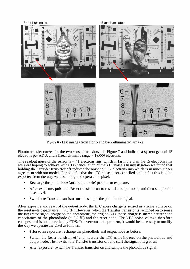
Figure 6 - Test images from front- and back-illuminated sensors
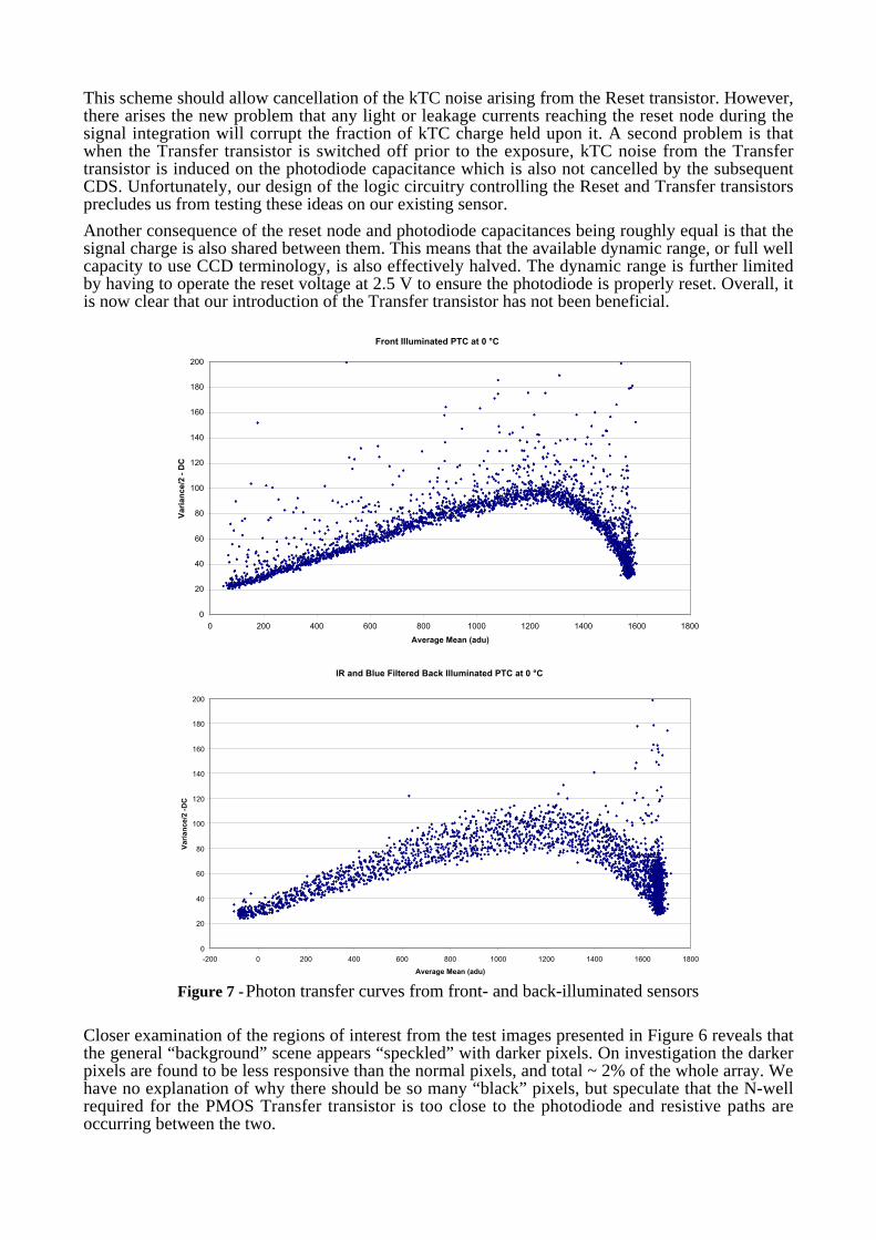
Photon transfer curves for the two sensors are shown in Figure 7 and indicate a system gain of 15electrons per ADU, and a linear dynamic range ~ 18,000 electrons.
The readout noise of the sensor is ~ 41 electrons rms, which is far more than the 15 electrons rmswe were hoping to achieve with CDS cancellation of the kTC noise. On investigation we found thatholding the Transfer transistor off reduces the noise to ~ 17 electrons rms which is in much closeragreement with our model. Our belief is that the kTC noise is not cancelled, and in fact this is to beexpected from the way we first thought to operate the pixel.
• Recharge the photodiode (and output node) prior to an exposure.
• After exposure, pulse the Reset transistor on to reset the output node, and then sample thereset level.
• Switch the Transfer transistor on and sample the photodiode signal.
After exposure and reset of the output node, the kTC noise charge is sensed as a noise voltage onthe reset node capacitance (~ 4.5 fF). However, when the Transfer transistor is switched on to sensethe integrated signal charge on the photodiode, the original kTC noise charge is shared between thecapacitance of the photodiode (~ 5.5 fF) and the reset node. The kTC noise voltage thereforechanges, and is not cancelled by CDS. To overcome this problem, it would be necessary to modifythe way we operate the pixel as follows.
• Prior to an exposure, recharge the photodiode and output node as before.
• Switch the Reset transistor off and measure the kTC noise induced on the photodiode andoutput node. Then switch the Transfer transistor off and start the signal integration.
• After exposure, switch the Transfer transistor on and sample the photodiode signal.
Front-illuminated Back-illuminated
This scheme should allow cancellation of the kTC noise arising from the Reset transistor. However,there arises the new problem that any light or leakage currents reaching the reset node during thesignal integration will corrupt the fraction of kTC charge held upon it. A second problem is thatwhen the Transfer transistor is switched off prior to the exposure, kTC noise from the Transfertransistor is induced on the photodiode capacitance which is also not cancelled by the subsequentCDS. Unfortunately, our design of the logic circuitry controlling the Reset and Transfer transistorsprecludes us from testing these ideas on our existing sensor.
Another consequence of the reset node and photodiode capacitances being roughly equal is that thesignal charge is also shared between them. This means that the available dynamic range, or full wellcapacity to use CCD terminology, is also effectively halved. The dynamic range is further limitedby having to operate the reset voltage at 2.5 V to ensure the photodiode is properly reset. Overall, itis now clear that our introduction of the Transfer transistor has not been beneficial.
Figure 7 - Photon transfer curves from front- and back-illuminated sensors
Closer examination of the regions of interest from the test images presented in Figure 6 reveals thatthe general “background” scene appears “speckled” with darker pixels. On investigation the darkerpixels are found to be less responsive than the normal pixels, and total ~ 2% of the whole array. Wehave no explanation of why there should be so many “black” pixels, but speculate that the N-wellrequired for the PMOS Transfer transistor is too close to the photodiode and resistive paths areoccurring between the two.
Front Illuminated PTC at 0 °C
0
20
40
60
80
100
120
140
160
180
200
0 200 400 600 800 1000 1200 1400 1600 1800
Average Mean (adu)
Var
ian
ce/2
- D
C
IR and Blue Filtered Back Illuminated PTC at 0 °C
0
20
40
60
80
100
120
140
160
180
200
-200 0 200 400 600 800 1000 1200 1400 1600 1800
Average Mean (adu)
Var
ian
ce/2
-D
C

In conclusion, we now regret our choice of pixel design for this sensor. The dynamic range has beenseverely compromised and the CDS cancellation of kTC noise has not worked as we first hoped. Onthe other hand, we have shown that a large-format sensor can be thinned uniformly to inside of an 8µm epitaxial layer. Further work is required to characterize the quantum efficiency and MTFperformance, but the results to date have been encouraging. The next step in our developmentprogramme will be to address how to maximize the pixel dynamic range.
5 - PLANS FOR THE NEXT SENSOR
We are planning to develop a new EUV-sensitive sensor of 2k x 2k 10 µm pixels for the ExtremeUltra-violet Spectrograph (EUS) on ESA’s Solar Orbiter. The original concept for the instrumentcalled for a 4k x 4k pixel detector format, hence our design of a 4k x 3k pixel prototype. However,subsequent optimization of the instrument’s conceptual design has seen this requirement relaxed toa 2k x 2k pixel format.In progress towards this goal, we have designed a test-structure consisting of six arrays of 512 x 51210 µm pixels. The larger pixel size allows us to use a 0.35 µm CMOS process, and we have selectedone from austriamicrosystems (AMS) that is fabricated on a relatively thick epitaxial layer of atleast 14 µm. Each of the arrays has been given a different pixel design to allow verification of ourmodels, and our progress towards optimizing a design for minimal system readout noise andmaximum dynamic range. These sensors will also be back-thinned for characterization at EUVwavelengths.All the pixels are 3-transistor type and so the only possibility for kTC noise cancellation will be toread the chip twice, before and after the signal integration, and perform the CDS off-chip. However[3] has shown that kTC noise can be reduced by using a soft-reset with the expectation that the kTCnoise contribution is closer to √kTC/2 rather than the normal √kTC. On its own, soft-reset will giverise to image lag with the result that one image is affected by the previous. However, [3] has shownthat this can be overcome by first using a hard-reset to ensure that all photodiodes are equally reset,followed by a soft-reset to gain the advantage in reset noise. This reset strategy is referred to as a“flushed-reset”, and we have implemented it on our new test-structure.
Figure 8 shows a schematic of the basic 3-transistor pixel with the additional circuitry required forthe flushed-reset. Figure 9 simplifies the schematic to illustrate how the circuit operates during thehard- and soft-reset phases.
During hard-reset, the Flush line is asserted connecting the Reset Voltage Bus between Mb1 andMb2’ (via Mfb). Mb1 and Mb2’ are biased so as to force the Reset Voltage Bus to some voltagelower than Vdd. When the Reset line is switched to Vdd, Mr will be overdriven and the pixel willbe hard-reset to the voltage on the Reset Voltage Bus.
The soft-reset is applied after allowing sufficient time for the hard-reset. Flush is de-asserted suchthat Mb2’ is no longer connected to the Reset Voltage Bus, and Mrf overrides Mb1, pulling theReset Voltage Bus up to Vdd. Mr is no longer overdriven, and so the reset becomes soft.
A second advantage of the flushed-reset scheme is that the difference in the voltage on the ResetVoltage Bus between hard- and soft-reset is coupled onto the photodiode during the soft-reset phaseand thus increases the dynamic range [3].

Figure 8 - Schematic of the flushed-reset 3-transistor pixel
Figure 9 - Flushed-reset operation
A floor-plan of the test-structure sensor is shown in Figure 10, and the different pixel types arelisted in Table 1. A prime objective is to explore the optimal pixel capacitance required forminimizing the total system noise and maximizing the dynamic range. Large capacitance isdesirable to maximize the photodiode full well capacity, and hence the overall dynamic range. Onthe other hand, small capacitance is needed to minimize kTC noise. Flushed-reset is expected tominimize the kTC noise contribution, and off-chip CDS may reduce it still further. Figure 11illustrates the full well capacity expected as a function of noise for varying capacitance.
Bias1
Bias2
Flush Vdd
Gnd
Row Select
Reset
Pixel
Column Bus
Reset Voltage Bus
Mrf Mb1
Mr
Msf Ms
Mb2’ Mb2
Mfb
Bias1
Bias2
Flush
Vdd
Gnd
Row Sel ect
Reset
Pixel
Column Bus Reset
Voltage Bus
Mb1
Mr
Msf Ms
Mb2’ Mb2
Mfb
Bias2
Flush Vdd
Gnd
Row Sel ect
Reset
Pixel
Column Bus
Mrf
Mr
Msf Ms
Mb2
Reset Voltage Bus
Hard Reset Soft Reset

Figure 10 - Floor plan of of our new test-structure chip
Pixel Name Photodiodecapacitance
Main Features
3TP3.3V 5 fF Simple 3-transistor pixel designed for minimal capacitanceand thus minimum kTC noise.
3TPLD3.3V 10 fF Same as 3TP3.3V but optimized with larger capacitancefor greater well capacity.
3TP3V5 5 fF 3.3 V and 5 V mixed voltage version of 3TP3.3V
3TP5V 5 fF All 5 V version of 3TP3.3V.
3TPEFW 20 fF Enhanced full-well version of 3TP3.3V with an addedcapacitor to maximize well capacity.
3TPSEFW 7 - 24 fF Switchable version of 3TPEFW to allow selectablephotodiode capacitance and hence well capacity.
Table 1- Pixel types of the 6-part 512 x 512 pixel test-structure
We have designed the first pixel (3TP3.3V) with minimal capacitance (~ 5 fF) and the second(3TPLD3.3V) with larger capacitance (~ 10 fF). Both of these pixels employ the standard 3.3 Vtransistors for the AMS 0.35 µm CMOS process. The third and fourth pixel types are variants of thebasic small-capacitance pixel; one with a mixture of 3.3 V and 5 V transistors (3TP3V5), and theother a full complement of 5 V transistors (3TP5V). These will be used to investigate whether 5 Vbiasing can be employed to increase the operating voltage range of the pixel, and hence the dynamicrange. There are side-effects with the 5 V transistors which suggest that the pixel characteristic isnot altogether straightforward to model. The fifth pixel (3TPEFW) has a capacitor added to thephotodiode to increase the overall capacitance to ~ 20 fF. Here we are maximizing the full wellcapacity in the knowledge that we will suffer more kTC noise. In the final pixel (3TPSEFW),shown in Figure 12, we have added a fourth transistor (Range) which allows the extra node
Key Row Selection Shift Registers & Steering Logic Multiplexer Control Shift Registers Analogue Multiplexers Pads
3TP3.3V
3TP5V 3TPSEFW
3TPLD3.3V 3TP3V5
3TPEFW
1
1
n
n
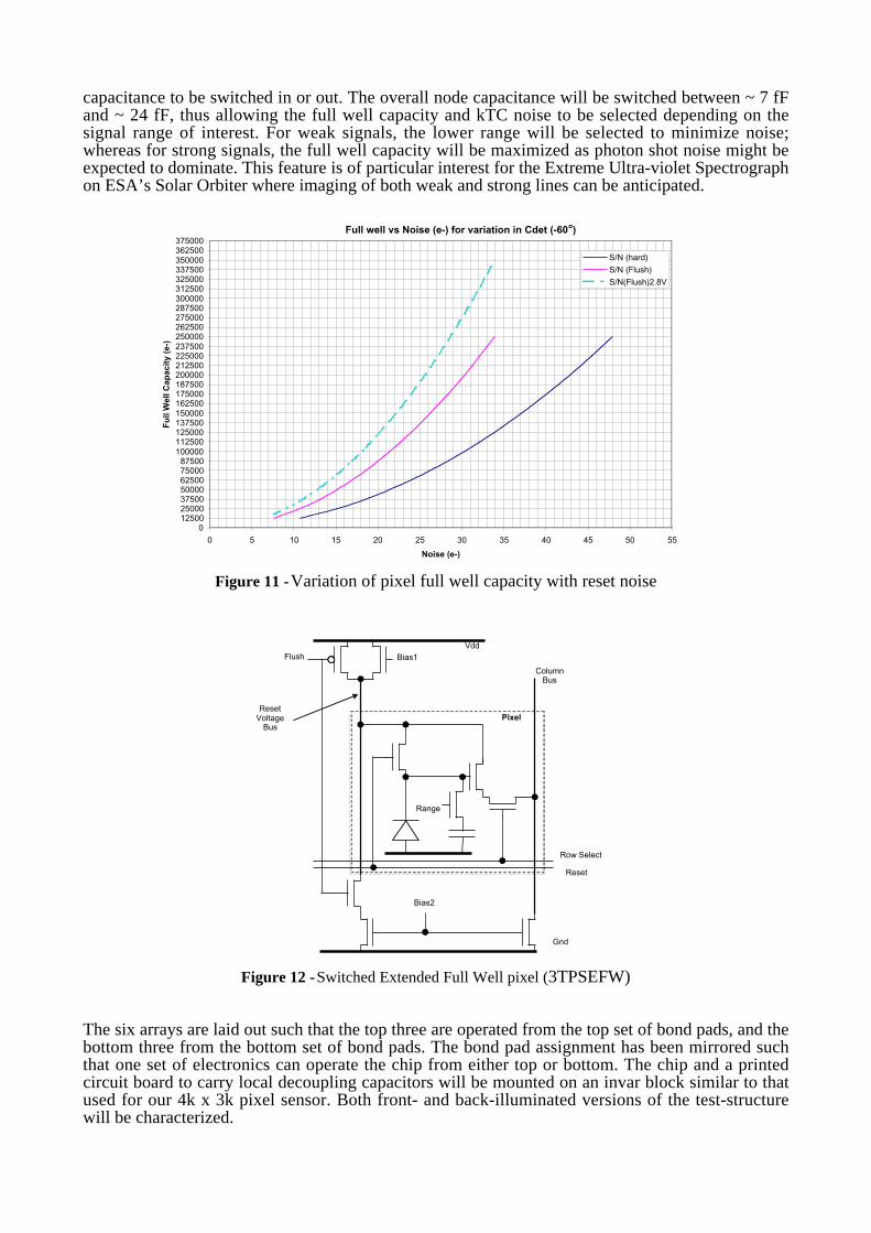
capacitance to be switched in or out. The overall node capacitance will be switched between ~ 7 fFand ~ 24 fF, thus allowing the full well capacity and kTC noise to be selected depending on thesignal range of interest. For weak signals, the lower range will be selected to minimize noise;whereas for strong signals, the full well capacity will be maximized as photon shot noise might beexpected to dominate. This feature is of particular interest for the Extreme Ultra-violet Spectrographon ESA’s Solar Orbiter where imaging of both weak and strong lines can be anticipated.
Figure 11 - Variation of pixel full well capacity with reset noise
Figure 12 - Switched Extended Full Well pixel (3TPSEFW)
The six arrays are laid out such that the top three are operated from the top set of bond pads, and thebottom three from the bottom set of bond pads. The bond pad assignment has been mirrored suchthat one set of electronics can operate the chip from either top or bottom. The chip and a printedcircuit board to carry local decoupling capacitors will be mounted on an invar block similar to thatused for our 4k x 3k pixel sensor. Both front- and back-illuminated versions of the test-structurewill be characterized.
Full well vs Noise (e-) for variation in Cdet (-60o)
012500250003750050000625007500087500
100000112500125000137500150000162500175000187500200000212500225000237500250000262500275000287500300000312500325000337500350000362500375000
0 5 10 15 20 25 30 35 40 45 50 55
Noise (e-)
Fu
ll W
ell C
apac
ity
(e-)
S/N (hard)
S/N (Flush)
S/N(Flush)2.8V
Bias1
Bias2
Flush Vdd
Gnd
Row Select
Reset
Pixel
Column Bus
Reset Voltage
Bus
Range

6 - CONCLUSIONS
We have demonstrated a large-format 4k x 3k pixel CMOS sensor with 5 µm pixels and thefeasibility of thinning for back-illumination. Further work is required to characterize the quantumefficiency and MTF performance of both the front- and back-illuminated sensors.
We have also presented our plans to develop a new EUV-sensitive sensor for the Extreme Ultra-violet Spectrograph on ESA’s Solar Orbiter, and in this the design of a new test-structure consistingof six arrays of 512 x 512 10 µm pixels. Each of the arrays has been given a different pixel designto allow verification of our models and progress towards optimizing well capacity and readoutnoise. These sensors will also be back-thinned for characterization at EUV wavelengths.
ACKNOWLEDGMENTS
The development of our 4k x 3k pixel sensor, our new test-structure, and the back-thinningprogramme with e2v technologies has been funded through a PPARC Rolling Grant to the SpaceScience and Technology Department (SSTD) at the Rutherford Appleton Laboratory. A Marshall,M Clapp, J King, D Drummond and J Rainnie of SSTD are acknowledged for the design andcommissioning of the data acquisition system.
7 - REFERENCES
[1] Prydderch, M. French, M., Holt, R., Marshall, A., Turchetta, R., Waltham, N., Eyles, C.,Mapson-Menard, H., Burt, D., Bell, R., and Pool, P. A 512x512 CMOS Monolithic ActivePixel Sensor with Integrated ADCs for Space Science, Nuclear Instrumentation and MethodsA 512 (2003), 358-367.
[2] Prydderch, M., Waltham, N., Morrissey, Q., Turchetta, R., and Pool P. A Large Area CMOSMonolithic Active Pixel Sensor for Extreme Ultra Violet Spectroscopy and Imaging. ProcSPIE Sensors and Camera Systems for Scientific, Industrial, and Digital PhotographyApplications V, Vol. 5301, San Jose, (2004), 175-185.
[3] Pain, B., Yang, G. Cunningham, T.J., Wrigley, C. and Hancock, H. An enhanced-performance CMOS imager with a flushed-reset photodiode pixel, IEEE Transactions onElectron Devices, Vol. 50, No. 1, (2003), 48-56.
➦ SOMMAIRE/SUMMARY ➦ Detectors and detection electronics