Embed Size (px)
Citation preview
〇Product structure : Silicon monolithic integrated circuit 〇This product has no designed protection against radioactive rays
.
1/25
TSZ02201-0M1M0FZ15130-1-2 © 2015 ROHM Co., Ltd. All rights reserved. 24.Mar.2016 Rev.003 TSZ22111 • 14 • 001
www.rohm.com
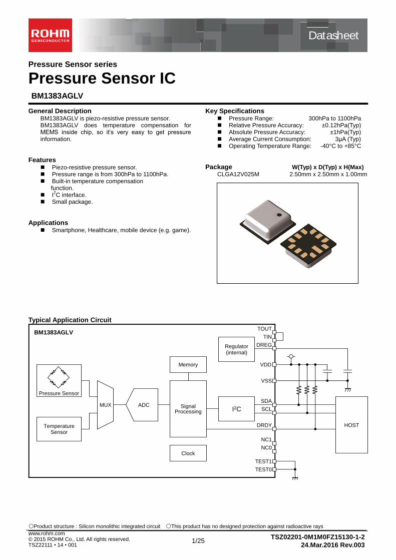
Pressure Sensor series
Pressure Sensor IC BM1383AGLV
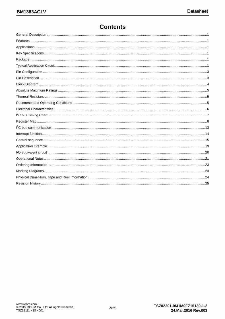
General Description BM1383AGLV is piezo-resistive pressure sensor. BM1383AGLV does temperature compensation for MEMS inside chip, so it’s very easy to get pressure information.
Features Piezo-resistive pressure sensor. Pressure range is from 300hPa to 1100hPa. Built-in temperature compensation
function. I
2C interface.
Small package.
Applications Smartphone, Healthcare, mobile device (e.g. game).
Key Specifications Pressure Range: 300hPa to 1100hPa Relative Pressure Accuracy: ±0.12hPa(Typ) Absolute Pressure Accuracy: ±1hPa(Typ) Average Current Consumption: 3μA (Typ) Operating Temperature Range: -40°C to +85°C
Package W(Typ) x D(Typ) x H(Max) CLGA12V025M 2.50mm x 2.50mm x 1.00mm
Typical Application Circuit
ADC
TemperatureSensor
MUX SignalProcessing I2C SCL
SDA
NC1
NC0
DRDY
Pressure Sensor
Memory
Clock
TOUT
TEST1
TEST0
TIN
VDD
VSS
DREG
HOST
BM1383AGLV
Regulator(internal)
Datasheet
2/25
TSZ02201-0M1M0FZ15130-1-2 © 2015 ROHM Co., Ltd. All rights reserved. 24.Mar.2016 Rev.003
www.rohm.com
TSZ22111 • 15 • 001
BM1383AGLV
Contents General Description ........................................................................................................................................................................ 1
Features.......................................................................................................................................................................................... 1
Applications .................................................................................................................................................................................... 1
Key Specifications ........................................................................................................................................................................... 1
Package .......................................................................................................................................................................................... 1
Typical Application Circuit ............................................................................................................................................................... 1
Pin Configuration ............................................................................................................................................................................ 3
Pin Description ................................................................................................................................................................................ 3
Block Diagram ................................................................................................................................................................................ 4
Absolute Maximum Ratings ............................................................................................................................................................ 5
Thermal Resistance ........................................................................................................................................................................ 5
Recommended Operating Conditions ............................................................................................................................................. 5
Electrical Characteristics................................................................................................................................................................. 6
I2C bus Timing Chart ....................................................................................................................................................................... 7
Register Map .................................................................................................................................................................................. 8
I2C bus communication ................................................................................................................................................................. 13
Interrupt function ........................................................................................................................................................................... 14
Control sequence .......................................................................................................................................................................... 15
Application Example ..................................................................................................................................................................... 19
I/O equivalent circuit ..................................................................................................................................................................... 20
Operational Notes ......................................................................................................................................................................... 21
Ordering Information ..................................................................................................................................................................... 23
Marking Diagrams ......................................................................................................................................................................... 23
Physical Dimension, Tape and Reel Information ........................................................................................................................... 24
Revision History ............................................................................................................................................................................ 25
3/25
TSZ02201-0M1M0FZ15130-1-2 © 2015 ROHM Co., Ltd. All rights reserved. 24.Mar.2016 Rev.003
www.rohm.com
TSZ22111 • 15 • 001
BM1383AGLV
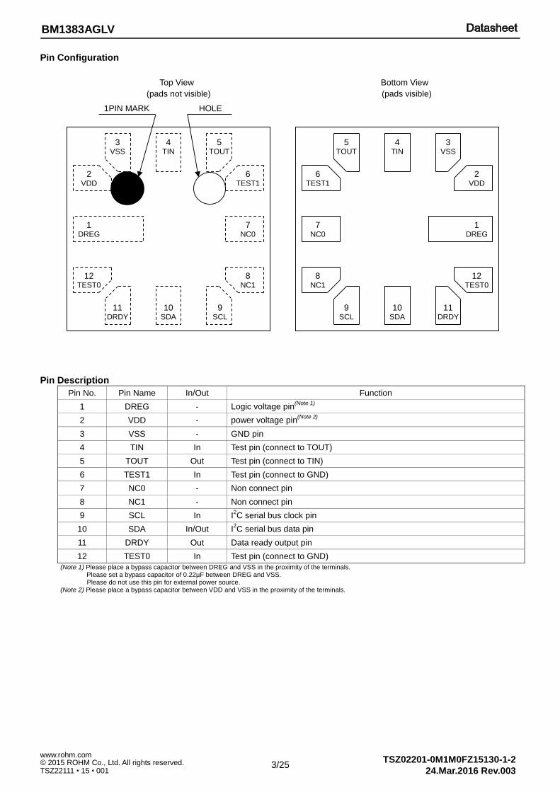
Pin Configuration
Pin Description
Pin No. Pin Name In/Out Function
1 DREG - Logic voltage pin(Note 1)
2 VDD - power voltage pin(Note 2)
3 VSS - GND pin
4 TIN In Test pin (connect to TOUT)
5 TOUT Out Test pin (connect to TIN)
6 TEST1 In Test pin (connect to GND)
7 NC0 - Non connect pin
8 NC1 - Non connect pin
9 SCL In I2C serial bus clock pin
10 SDA In/Out I2C serial bus data pin
11 DRDY Out Data ready output pin
12 TEST0 In Test pin (connect to GND)
(Note 1) Please place a bypass capacitor between DREG and VSS in the proximity of the terminals. Please set a bypass capacitor of 0.22µF between DREG and VSS. Please do not use this pin for external power source. (Note 2) Please place a bypass capacitor between VDD and VSS in the proximity of the terminals.
Top View Bottom View
(pads not visible) (pads visible)
7NC0
8NC1
9SCL
10SDA
11DRDY
12TEST0
1DREG
2VDD
3VSS
4TIN
5TOUT
6TEST1
HOLE
7NC0
8NC1
6TEST1
12TEST0
1DREG
2VDD
9SCL
10SDA
11DRDY
3VSS
4TIN
5TOUT
1PIN MARK
4/25
TSZ02201-0M1M0FZ15130-1-2 © 2015 ROHM Co., Ltd. All rights reserved. 24.Mar.2016 Rev.003
www.rohm.com
TSZ22111 • 15 • 001
BM1383AGLV
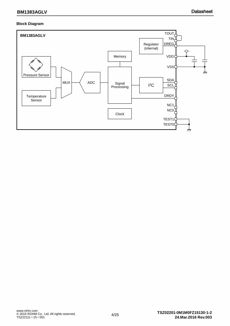
Block Diagram
ADC
TemperatureSensor
MUX SignalProcessing I2C SCL
SDA
NC1
NC0
DRDY
Pressure Sensor
Memory
Clock
TOUT
TEST1
TEST0
TIN
VDD
VSS
DREG
BM1383AGLV
Regulator(internal)
5/25
TSZ02201-0M1M0FZ15130-1-2 © 2015 ROHM Co., Ltd. All rights reserved. 24.Mar.2016 Rev.003
www.rohm.com
TSZ22111 • 15 • 001
BM1383AGLV
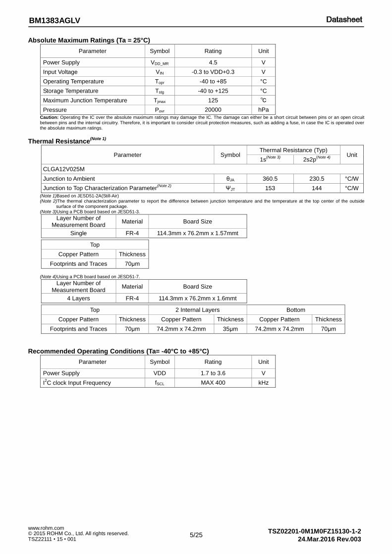
Absolute Maximum Ratings (Ta = 25°C)
Parameter Symbol Rating Unit
Power Supply VDD_MR 4.5 V
Input Voltage VIN -0.3 to VDD+0.3 V
Operating Temperature Topr -40 to +85 °C
Storage Temperature Tstg -40 to +125 °C
Maximum Junction Temperature Tjmax 125 ℃
Pressure Povr 20000 hPa
Caution: Operating the IC over the absolute maximum ratings may damage the IC. The damage can either be a short circuit between pins or an open circuit between pins and the internal circuitry. Therefore, it is important to consider circuit protection measures, such as adding a fuse, in case the IC is operated over the absolute maximum ratings.
Thermal Resistance(Note 1)
Parameter Symbol Thermal Resistance (Typ)
Unit 1s
(Note 3) 2s2p
(Note 4)
CLGA12V025M
Junction to Ambient θJA 360.5 230.5 °C/W
Junction to Top Characterization Parameter(Note 2)
ΨJT 153 144 °C/W
(Note 1)Based on JESD51-2A(Still-Air) (Note 2)The thermal characterization parameter to report the difference between junction temperature and the temperature at the top center of the outside
surface of the component package. (Note 3)Using a PCB board based on JESD51-3.
Layer Number of Measurement Board
Material Board Size
Single FR-4 114.3mm x 76.2mm x 1.57mmt
Top
Copper Pattern Thickness
Footprints and Traces 70μm
(Note 4)Using a PCB board based on JESD51-7.
Layer Number of Measurement Board
Material Board Size
4 Layers FR-4 114.3mm x 76.2mm x 1.6mmt
Top 2 Internal Layers Bottom
Copper Pattern Thickness Copper Pattern Thickness Copper Pattern Thickness
Footprints and Traces 70μm 74.2mm x 74.2mm 35μm 74.2mm x 74.2mm 70μm
Recommended Operating Conditions (Ta= -40°C to +85°C)
Parameter Symbol Rating Unit
Power Supply VDD 1.7 to 3.6 V
I2C clock Input Frequency fSCL MAX 400 kHz
6/25
TSZ02201-0M1M0FZ15130-1-2 © 2015 ROHM Co., Ltd. All rights reserved. 24.Mar.2016 Rev.003
www.rohm.com
TSZ22111 • 15 • 001
BM1383AGLV
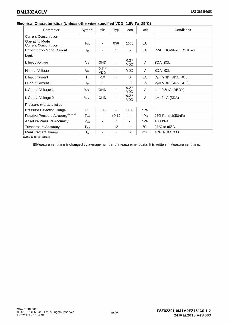
Electrical Characteristics (Unless otherwise specified VDD=1.8V Ta=25°C)
Parameter Symbol Min Typ Max Unit Conditions
Current Consumption
Operating Mode Current Consumption
Iddp - 650 1000 µA
Power Down Mode Current Iss - 1 5 µA PWR_DOWN=0, RSTB=0
Logic
L Input Voltage VIL GND - 0.3 * VDD
V SDA, SCL
H Input Voltage VIH 0.7 * VDD
- VDD V SDA, SCL
L Input Current IIL -10 - 0 μA VIL= GND (SDA, SCL)
H Input Current IIH 0 - 10 μA VIH= VDD (SDA, SCL)
L Output Voltage 1 VOL1 GND - 0.2 * VDD
V IL= -0.3mA (DRDY)
L Output Voltage 2 VOL2 GND - 0.2 * VDD
V IL= -3mA (SDA)
Pressure characteristics
Pressure Detection Range PR 300 - 1100 hPa
Relative Pressure Accuracy(Note 1)
Prel - ±0.12 - hPa 950hPa to 1050hPa
Absolute Pressure Accuracy Pabs - ±1 - hPa 1000hPa
Temperature Accuracy Tabs - ±2 - °C 25°C to 85°C
Measurement Time※ Tm - - 6 ms AVE_NUM=000
(Note 1) Target values
※Measurement time is changed by average number of measurement data. It is written in Measurement time.
7/25
TSZ02201-0M1M0FZ15130-1-2 © 2015 ROHM Co., Ltd. All rights reserved. 24.Mar.2016 Rev.003
www.rohm.com
TSZ22111 • 15 • 001
BM1383AGLV
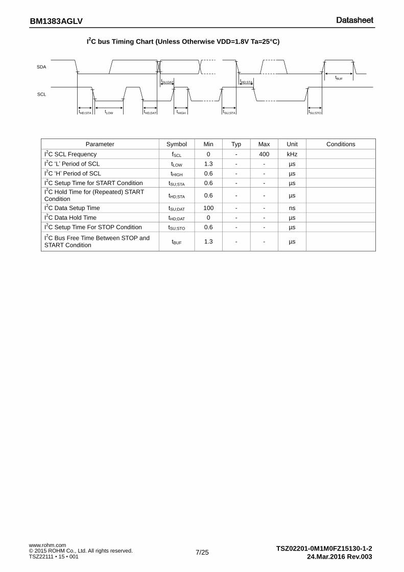
I2C bus Timing Chart (Unless Otherwise VDD=1.8V Ta=25°C)
Parameter Symbol Min Typ Max Unit Conditions
I2C SCL Frequency fSCL 0 - 400 kHz
I2C ‘L’ Period of SCL tLOW 1.3 - - µs
I2C ‘H’ Period of SCL tHIGH 0.6 - - µs
I2C Setup Time for START Condition tSU;STA 0.6 - - µs
I2C Hold Time for (Repeated) START
Condition tHD;STA 0.6 - - µs
I2C Data Setup Time tSU;DAT 100 - - ns
I2C Data Hold Time tHD;DAT 0 - - µs
I2C Setup Time For STOP Condition tSU;STO 0.6 - - µs
I2C Bus Free Time Between STOP and
START Condition tBUF 1.3 - - µs
SDA
SCL
tHD;STA tLOW tHD;DAT
tSU;DAT
tHIGH tSU;STA
tHD;STA
tSU;STO
tBUF
8/25
TSZ02201-0M1M0FZ15130-1-2 © 2015 ROHM Co., Ltd. All rights reserved. 24.Mar.2016 Rev.003
www.rohm.com
TSZ22111 • 15 • 001
BM1383AGLV
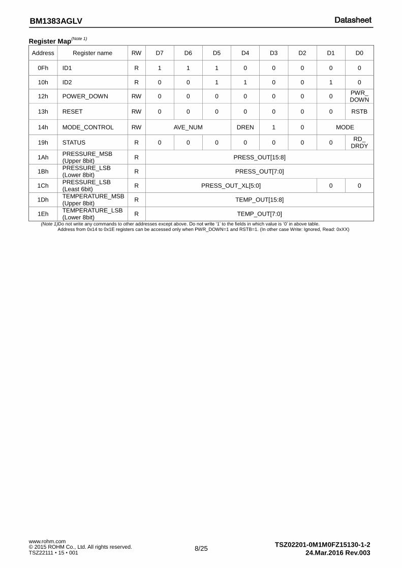
Register Map(Note 1)
Address Register name RW D7 D6 D5 D4 D3 D2 D1 D0
0Fh ID1 R 1 1 1 0 0 0 0 0
10h ID2 R 0 0 1 1 0 0 1 0
12h POWER_DOWN RW 0 0 0 0 0 0 0 PWR_ DOWN
13h RESET RW 0 0 0 0 0 0 0 RSTB
14h MODE_CONTROL RW AVE_NUM DREN 1 0 MODE
19h STATUS R 0 0 0 0 0 0 0 RD_
DRDY
1Ah PRESSURE_MSB (Upper 8bit)
R PRESS_OUT[15:8]
1Bh PRESSURE_LSB (Lower 8bit)
R PRESS_OUT[7:0]
1Ch PRESSURE_LSB (Least 6bit)
R PRESS_OUT_XL[5:0] 0 0
1Dh TEMPERATURE_MSB (Upper 8bit)
R TEMP_OUT[15:8]
1Eh TEMPERATURE_LSB (Lower 8bit)
R TEMP_OUT[7:0]
(Note 1)Do not write any commands to other addresses except above. Do not write ‘1’ to the fields in which value is ‘0’ in above table. Address from 0x14 to 0x1E registers can be accessed only when PWR_DOWN=1 and RSTB=1. (In other case Write: Ignored, Read: 0xXX)
9/25
TSZ02201-0M1M0FZ15130-1-2 © 2015 ROHM Co., Ltd. All rights reserved. 24.Mar.2016 Rev.003
www.rohm.com
TSZ22111 • 15 • 001
BM1383AGLV
○ID1(0Fh)
Field Bit TYPE Description
ID1 7 : 0 R 11100000
default value E0h
○ID2(10h)
Field Bit TYPE Description
ID2 7 : 0 R 00110010
default value 32h ○POWER_DOWN(12h)
Field Bit TYPE Description
Reserved 7 : 1 RW Reserved Write “0”
PWR_DOWN 0 RW 0: power down 1: active
default value 00h
○RESET(13h)
Field Bit TYPE Description
Reserved 7 : 1 RW Reserved Write “0”
RSTB 0 RW 0: Measurement control block is reset 1: Measurement control block is active
default value 00h
10/25
TSZ02201-0M1M0FZ15130-1-2 © 2015 ROHM Co., Ltd. All rights reserved. 24.Mar.2016 Rev.003
www.rohm.com
TSZ22111 • 15 • 001
BM1383AGLV
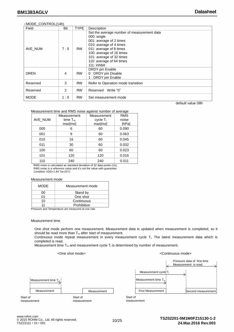
○MODE_CONTROL(14h)
Field Bit TYPE Description
AVE_NUM 7 : 5 RW
Set the average number of measurement data 000: single 001: average of 2 times 010: average of 4 times 011: average of 8 times 100: average of 16 times 101: average of 32 times 110: average of 64 times 111: inhibit
DREN 4 RW DRDY pin Enable 0 : DRDY pin Disable 1 : DRDY pin Enable
Reserved 3 RW Refer to Operation mode transition
Reserved 2 RW Reserved Write “0”
MODE 1 : 0 RW Set measurement mode
default value 08h
Measurement time and RMS noise against number of average
AVE_NUM Measurement
time Tm max[ms]
Measurement cycle Ti max[ms]
RMS noise [hPa]
000 6 60 0.090
001 9 60 0.063
010 16 60 0.045
011 30 60 0.032
100 60 60 0.023
101 120 120 0.016
110 240 240 0.011 RMS noise is calculated as standard deviation of 32 data points (1σ). RMS noise is a reference value and it’s not the value with guarantee. Condition VDD=1.8V Ta=25°C
Measurement mode
MODE Measurement mode
00 Stand by
01 One shot
10 Continuous
11 Prohibition Pressure and Temperature are measured at one rate
Measurement time
One shot mode perform one measurement. Measurement data is updated when measurement is completed, so it should be read more than Tm after start of measurement. Continuous mode repeat measurement in every measurement cycle Ti. The latest measurement data which is completed is read. Measurement time Tm and measurement cycle Ti is determined by number of measurement. <One shot mode> <Continuous mode>
First Measurement
Measurement time Tm
Measurement cycle Ti
Second measurement
Start of measurement
Measurement time Tm
Start of measurement
Start of measurement
Measurement Measurement
Pressure data of first time Measurement is read.
11/25
TSZ02201-0M1M0FZ15130-1-2 © 2015 ROHM Co., Ltd. All rights reserved. 24.Mar.2016 Rev.003
www.rohm.com
TSZ22111 • 15 • 001
BM1383AGLV
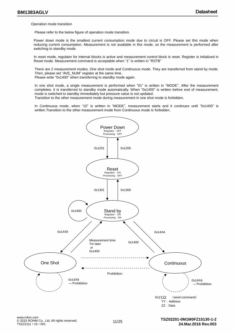
Operation mode transition
Please refer to the below figure of operation mode transition.
Power down mode is the smallest current consumption mode due to circuit is OFF. Please set this mode when reducing current consumption. Measurement is not available in this mode, so the measurement is performed after switching to standby mode.
In reset mode, regulator for internal blocks is active and measurement control block is reset. Register is initialized in Reset mode. Measurement command is acceptable when “1” is written in “RSTB”
There are 2 measurement modes. One shot mode and Continuous mode. They are transferred from stand by mode. Then, please set “AVE_NUM” register at the same time. Please write “0x1400” when transferring to standby mode again. In one shot mode, a single measurement is performed when “01” is written in “MODE”. After the measurement completes, it is transferred to standby mode automatically. When “0x1400” is written before end of measurement, mode is switched to standby immediately but pressure value is not updated. Transition to the other measurement mode during measurement in one shot mode is forbidden. In Continuous mode, when “10” is written in “MODE”, measurement starts and it continues until “0x1400” is written.Transition to the other measurement mode from Continuous mode is forbidden.
0x14X9
Measurement timeTm lateror
0x1400
0x14XA
0x1400
One Shot Continuous
Stand by
Reset
0x1301 0x1300
Power Down
0x1201 0x1200
0x1400
0x14XA→ Prohibition
Prohibition
Regulator:OFF
Processing:OFF
Regulator:ON
Processing:OFF
Regulator:ON
Processing:ON
0x14X9→ Prohibition
0xYYZZ (send command)
YY:Address
ZZ:Data
12/25
TSZ02201-0M1M0FZ15130-1-2 © 2015 ROHM Co., Ltd. All rights reserved. 24.Mar.2016 Rev.003
www.rohm.com
TSZ22111 • 15 • 001
BM1383AGLV
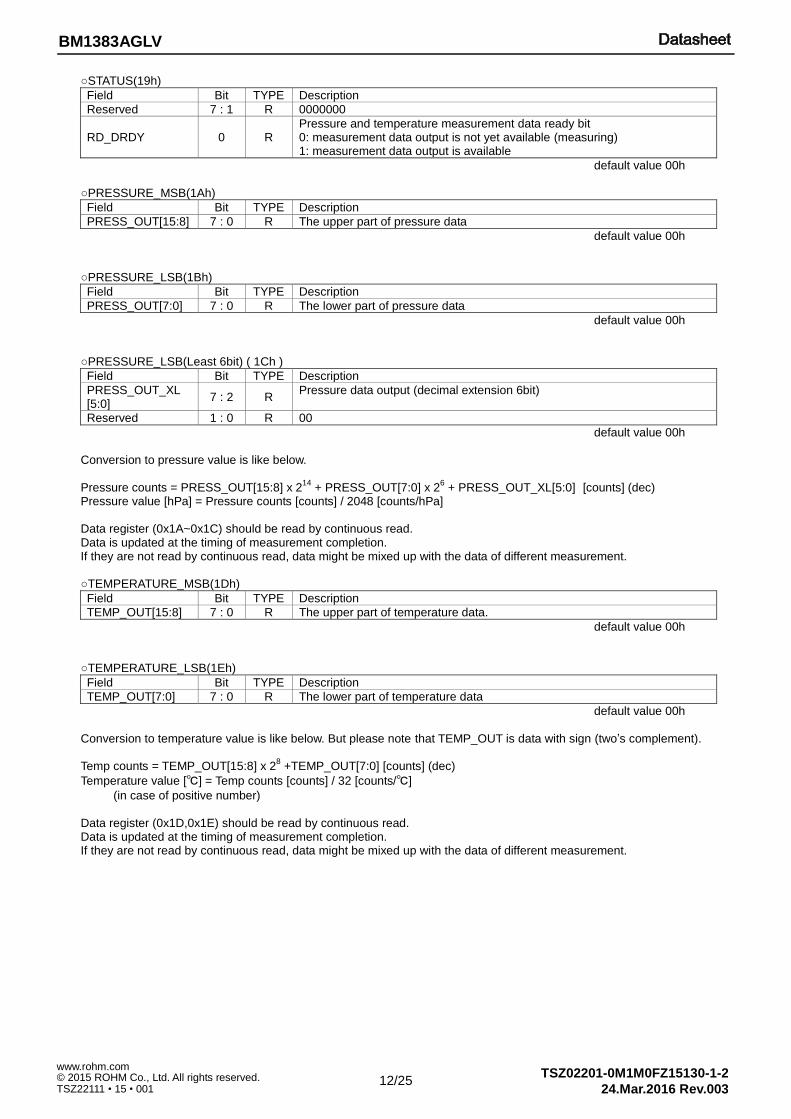
○STATUS(19h)
Field Bit TYPE Description
Reserved 7 : 1 R 0000000
RD_DRDY 0 R Pressure and temperature measurement data ready bit 0: measurement data output is not yet available (measuring) 1: measurement data output is available
default value 00h
○PRESSURE_MSB(1Ah)
Field Bit TYPE Description
PRESS_OUT[15:8] 7 : 0 R The upper part of pressure data
default value 00h
○PRESSURE_LSB(1Bh)
Field Bit TYPE Description
PRESS_OUT[7:0] 7 : 0 R The lower part of pressure data
default value 00h
○PRESSURE_LSB(Least 6bit) ( 1Ch )
Field Bit TYPE Description
PRESS_OUT_XL [5:0]
7 : 2 R Pressure data output (decimal extension 6bit)
Reserved 1 : 0 R 00
default value 00h Conversion to pressure value is like below. Pressure counts = PRESS_OUT[15:8] x 2
14 + PRESS_OUT[7:0] x 2
6 + PRESS_OUT_XL[5:0] [counts] (dec)
Pressure value [hPa] = Pressure counts [counts] / 2048 [counts/hPa] Data register (0x1A~0x1C) should be read by continuous read. Data is updated at the timing of measurement completion. If they are not read by continuous read, data might be mixed up with the data of different measurement. ○TEMPERATURE_MSB(1Dh)
Field Bit TYPE Description
TEMP_OUT[15:8] 7 : 0 R The upper part of temperature data.
default value 00h
○TEMPERATURE_LSB(1Eh)
Field Bit TYPE Description
TEMP_OUT[7:0] 7 : 0 R The lower part of temperature data
default value 00h
Conversion to temperature value is like below. But please note that TEMP_OUT is data with sign (two’s complement). Temp counts = TEMP_OUT[15:8] x 2
8 +TEMP_OUT[7:0] [counts] (dec)
Temperature value [℃] = Temp counts [counts] / 32 [counts/℃]
(in case of positive number) Data register (0x1D,0x1E) should be read by continuous read. Data is updated at the timing of measurement completion. If they are not read by continuous read, data might be mixed up with the data of different measurement.
13/25
TSZ02201-0M1M0FZ15130-1-2 © 2015 ROHM Co., Ltd. All rights reserved. 24.Mar.2016 Rev.003
www.rohm.com
TSZ22111 • 15 • 001
BM1383AGLV
I2C bus communication
1. Slave address : “1011101”
2. Write format
(1) Case of indicating only register address
ST Slave Address W 0
ACK Indicate register address ACK SP
(2) Case of writing data register after indicating register address
ST Slave Address W 0
ACK Indicate register address ACK
Data specified at register address field
ACK ・・・・・・ ACK Data specified at register
address field + N ACK SP
3. Read format
(1) Case of continuous reading data after indicating register address (Master issues restart condition)
ST Slave Address W 0
ACK Indicate register address ACK
ST Slave Address R 1
ACK Data specified at register
address field ACK
Data specified at register address field + 1
ACK ・・・・・・ ACK Data specified at register
address field + N NACK SP
(2) Case of continuous reading data
ST Slave Address R 1
ACK Data specified at register
address field ACK
Data specified at register address field + 1
ACK ・・・・・・ ACK Data specified at register
address field + N NACK SP
from master to slave from slave to master
14/25
TSZ02201-0M1M0FZ15130-1-2 © 2015 ROHM Co., Ltd. All rights reserved. 24.Mar.2016 Rev.003
www.rohm.com
TSZ22111 • 15 • 001
BM1383AGLV
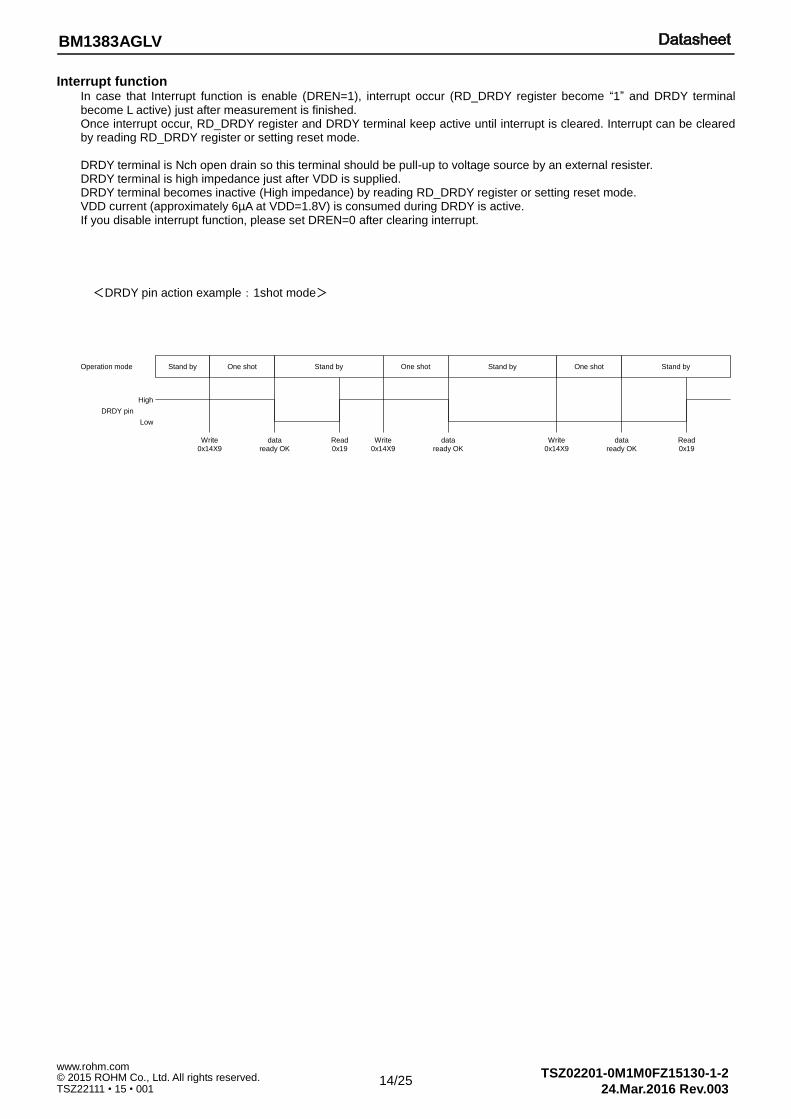
Interrupt function In case that Interrupt function is enable (DREN=1), interrupt occur (RD_DRDY register become “1” and DRDY terminal become L active) just after measurement is finished. Once interrupt occur, RD_DRDY register and DRDY terminal keep active until interrupt is cleared. Interrupt can be cleared by reading RD_DRDY register or setting reset mode. DRDY terminal is Nch open drain so this terminal should be pull-up to voltage source by an external resister. DRDY terminal is high impedance just after VDD is supplied. DRDY terminal becomes inactive (High impedance) by reading RD_DRDY register or setting reset mode. VDD current (approximately 6µA at VDD=1.8V) is consumed during DRDY is active. If you disable interrupt function, please set DREN=0 after clearing interrupt.
<DRDY pin action example:1shot mode>
Stand by One shot
High
Low
DRDY pin
Write0x14X9
Stand by
dataready OK
Read0x19
One shot Stand by One shot Stand by
Read0x19
Write0x14X9
Write0x14X9
Operation mode
dataready OK
dataready OK
15/25
TSZ02201-0M1M0FZ15130-1-2 © 2015 ROHM Co., Ltd. All rights reserved. 24.Mar.2016 Rev.003
www.rohm.com
TSZ22111 • 15 • 001
BM1383AGLV
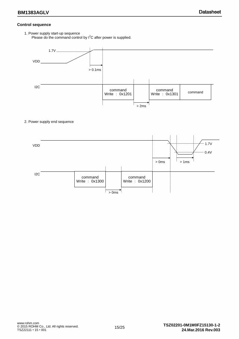
Control sequence
1. Power supply start-up sequence Please do the command control by I
2C after power is supplied.
2. Power supply end sequence
> 2ms
VDD
I2Ccommand
Write : 0x1201
> 0.1ms
commandWrite : 0x1301
command
1.7V
commandWrite : 0x1200
commandWrite : 0x1300
> 0ms
> 0ms
VDD
I2C
1.7V
0.4V
> 1ms
16/25
TSZ02201-0M1M0FZ15130-1-2 © 2015 ROHM Co., Ltd. All rights reserved. 24.Mar.2016 Rev.003
www.rohm.com
TSZ22111 • 15 • 001
BM1383AGLV
3. Starting sequence
power supply
POWER_DOWN setting
Write : 0x1201
RESET setting
Write : 0x1301
Completion of starting sequence
release Power down
release Reset mode
:
:
wait for morethan 2ms
wait for morethan 0.1ms
4. Measurement sequence: One Shot Mode
Starting sequence
MODE_CONTROL setting
Write : 0x14X9 (DREN=1)
DRDY terminal
L
H
read PRESSURE
Read : 0x1A~0x1C
Measurementcomplestion
measurement mode setting:
wait interrupt(DRDY='L') or measurement end:
read Pressure data:
Enable DRDY?noyes
MODE_CONTROL setting
Write : 0x14X9 (DREN=0)
wait for the end of measurement
no
yes
read STATUS
Read : 0x19
check interrupt status
DRDY terminal is set to 'H' by reading.:
17/25
TSZ02201-0M1M0FZ15130-1-2 © 2015 ROHM Co., Ltd. All rights reserved. 24.Mar.2016 Rev.003
www.rohm.com
TSZ22111 • 15 • 001
BM1383AGLV
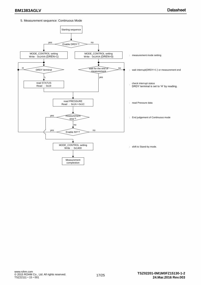
5. Measurement sequence: Continuous Mode
Starting sequence
MODE_CONTROL setting
Write:0x14XA (DREN=1)
DRDY terminal
L
H
read PRESSURE
Read : 0x1A~0x1C
Measurementcomplestion
measurement mode setting:
wait interrupt(DRDY='L') or measurement end:
read Pressure data:
Enable DRDY?noyes
MODE_CONTROL setting
Write:0x14XA (DREN=0)
wait for the end of measurement
no
yes
read STATUS
Read : 0x19:
MODE_CONTROL setting
Write : 0x1400shift to Stand-by mode.:
yes
no
measurement
stop?
Enable INT?noyes
End judgement of Continuous mode:
check interrupt status
DRDY terminal is set to 'H' by reading.
18/25
TSZ02201-0M1M0FZ15130-1-2 © 2015 ROHM Co., Ltd. All rights reserved. 24.Mar.2016 Rev.003
www.rohm.com
TSZ22111 • 15 • 001
BM1383AGLV
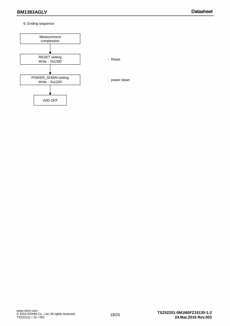
6. Ending sequence
Measurementcomplestion
RESET setting
Write : 0x1300
POWER_DOWN setting
Write : 0x1200
VDD OFF
Reset:
power down:
19/25
TSZ02201-0M1M0FZ15130-1-2 © 2015 ROHM Co., Ltd. All rights reserved. 24.Mar.2016 Rev.003
www.rohm.com
TSZ22111 • 15 • 001
BM1383AGLV
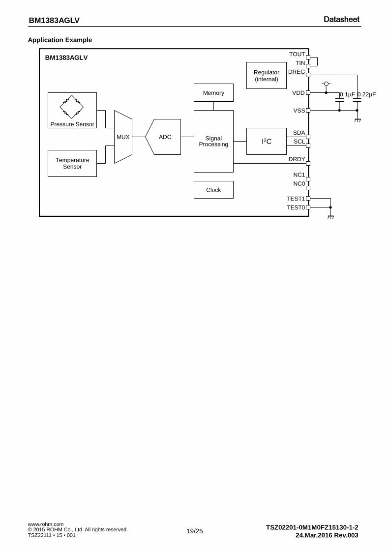
Application Example
ADC
TemperatureSensor
MUX SignalProcessing I2C SCL
SDA
NC1
NC0
DRDY
Pressure Sensor
Memory
Clock
TOUT
TEST1
TEST0
TIN
VDD
VSS
DREG
BM1383AGLV
Regulator(internal)
0.22µF 0.1µF
20/25
TSZ02201-0M1M0FZ15130-1-2 © 2015 ROHM Co., Ltd. All rights reserved. 24.Mar.2016 Rev.003
www.rohm.com
TSZ22111 • 15 • 001
BM1383AGLV
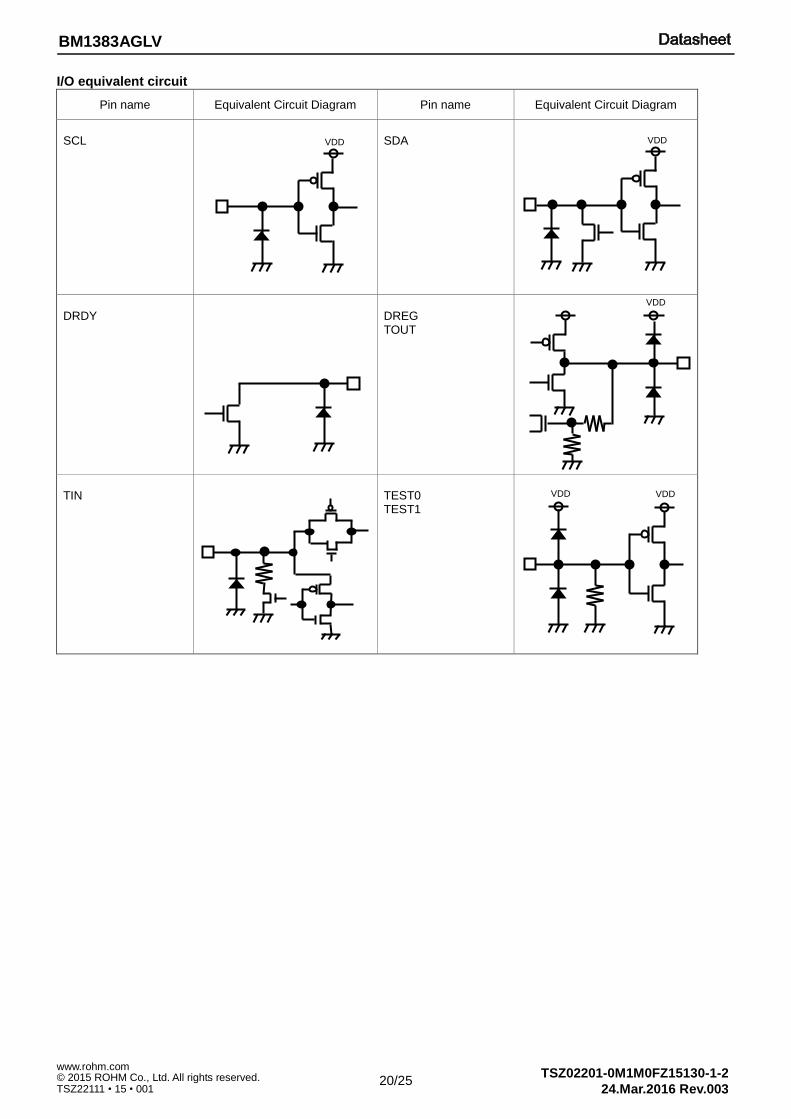
I/O equivalent circuit
Pin name Equivalent Circuit Diagram Pin name Equivalent Circuit Diagram
SCL
SDA
DRDY
DREG TOUT
TIN
TEST0 TEST1
VDD VDD
VDD VDD
VDD
21/25
TSZ02201-0M1M0FZ15130-1-2 © 2015 ROHM Co., Ltd. All rights reserved. 24.Mar.2016 Rev.003
www.rohm.com
TSZ22111 • 15 • 001
BM1383AGLV
Operational Notes
1. Reverse Connection of Power Supply
Connecting the power supply in reverse polarity can damage the IC. Take precautions against reverse polarity when connecting the power supply, such as mounting an external diode between the power supply and the IC’s power supply pins.
2. Power Supply Lines
Design the PCB layout pattern to provide low impedance supply lines. Furthermore, connect a capacitor to ground at all power supply pins. Consider the effect of temperature and aging on the capacitance value when using electrolytic capacitors.
3. Ground Voltage
Ensure that no pins are at a voltage below that of the ground pin at any time, even during transient condition.
4. Ground Wiring Pattern
When using both small-signal and large-current ground traces, the two ground traces should be routed separately but connected to a single ground at the reference point of the application board to avoid fluctuations in the small-signal ground caused by large currents. Also ensure that the ground traces of external components do not cause variations on the ground voltage. The ground lines must be as short and thick as possible to reduce line impedance.
5. Thermal Consideration
Should by any chance the maximum junction temperature rating be exceeded the rise in temperature of the chip may result in deterioration of the properties of the chip. In case of exceeding this absolute maximum rating, increase the board size and copper area to prevent exceeding the maximum junction temperature rating.
6. Recommended Operating Conditions
These conditions represent a range within which the expected characteristics of the IC can be approximately obtained. The electrical characteristics are guaranteed under the conditions of each parameter.
7. Inrush Current
When power is first supplied to the IC, it is possible that the internal logic may be unstable and inrush current may flow instantaneously due to the internal powering sequence and delays, especially if the IC has more than one power supply. Therefore, give special consideration to power coupling capacitance, power wiring, width of ground wiring, and routing of connections.
8. Operation Under Strong Electromagnetic Field
Operating the IC in the presence of a strong electromagnetic field may cause the IC to malfunction.
9. Testing on Application Boards
When testing the IC on an application board, connecting a capacitor directly to a low-impedance output pin may subject the IC to stress. Always discharge capacitors completely after each process or step. The IC’s power supply should always be turned off completely before connecting or removing it from the test setup during the inspection process. To prevent damage from static discharge, ground the IC during assembly and use similar precautions during transport and storage.
10. Inter-pin Short and Mounting Errors
Ensure that the direction and position are correct when mounting the IC on the PCB. Incorrect mounting may result in damaging the IC. Avoid nearby pins being shorted to each other especially to ground, power supply and output pin. Inter-pin shorts could be due to many reasons such as metal particles, water droplets (in very humid environment) and unintentional solder bridge deposited in between pins during assembly to name a few.
11. Unused Input Pins
Input pins of an IC are often connected to the gate of a MOS transistor. The gate has extremely high impedance and extremely low capacitance. If left unconnected, the electric field from the outside can easily charge it. The small charge acquired in this way is enough to produce a significant effect on the conduction through the transistor and cause unexpected operation of the IC. So unless otherwise specified, unused input pins should be connected to the power supply or ground line.

22/25
TSZ02201-0M1M0FZ15130-1-2 © 2015 ROHM Co., Ltd. All rights reserved. 24.Mar.2016 Rev.003
www.rohm.com
TSZ22111 • 15 • 001
BM1383AGLV
Operational Notes – continued
12. Regarding the Input Pin of the IC
In the construction of this IC, P-N junctions are inevitably formed creating parasitic diodes or transistors. The operation of these parasitic elements can result in mutual interference among circuits, operational faults, or physical damage. Therefore, conditions which cause these parasitic elements to operate, such as applying a voltage to an input pin lower than the ground voltage should be avoided. Furthermore, do not apply a voltage to the input pins when no power supply voltage is applied to the IC. Even if the power supply voltage is applied, make sure that the input pins have voltages within the values specified in the electrical characteristics of this IC.
13. Ceramic Capacitor
When using a ceramic capacitor, determine the dielectric constant considering the change of capacitance with temperature and the decrease in nominal capacitance due to DC bias and others.
14. Disturbance light
In a device where a portion of silicon is exposed to light such as in a WL-CSP, IC characteristics may be affected due to photoelectric effect. For this reason, it is recommended to come up with countermeasures that will prevent the chip from being exposed to light.
23/25
TSZ02201-0M1M0FZ15130-1-2 © 2015 ROHM Co., Ltd. All rights reserved. 24.Mar.2016 Rev.003
www.rohm.com
TSZ22111 • 15 • 001
BM1383AGLV
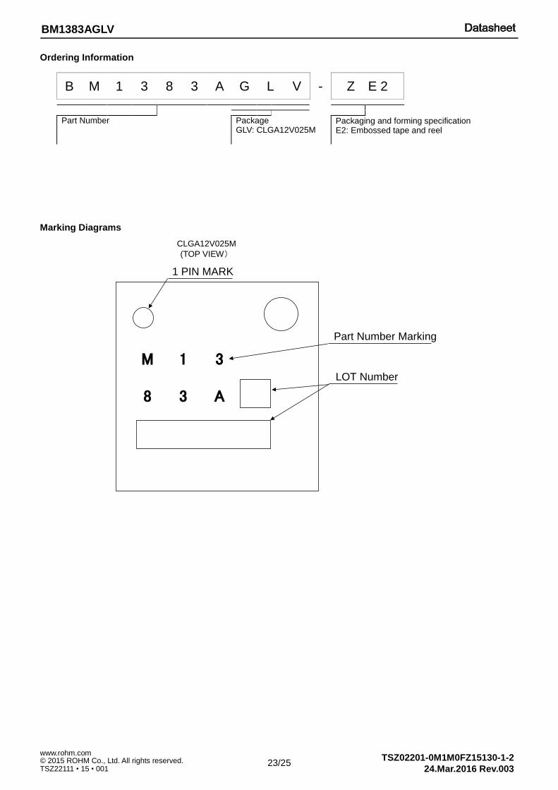
Ordering Information
B M 1 3 8 3 A G L V - Z E 2
Part Number
Package GLV: CLGA12V025M
Packaging and forming specification E2: Embossed tape and reel
Marking Diagrams
M 1 3
8
1 PIN MARK
LOT Number
Part Number Marking
3 A
CLGA12V025M
(TOP VIEW)
24/25
TSZ02201-0M1M0FZ15130-1-2 © 2015 ROHM Co., Ltd. All rights reserved. 24.Mar.2016 Rev.003
www.rohm.com
TSZ22111 • 15 • 001
BM1383AGLV
Physical Dimension, Tape and Reel Information
Package Name CLGA12V025M
25/25
TSZ02201-0M1M0FZ15130-1-2 © 2015 ROHM Co., Ltd. All rights reserved. 24.Mar.2016 Rev.003
www.rohm.com
TSZ22111 • 15 • 001
BM1383AGLV
Revision History
Date Revision Changes
17.Nov.2015 001 New Release
30.Mar.2016 002
P1 modify Typical Application Circuit P3 modify Pin Description P4 modify Block Diagram P5 modify Absolute Maximum Ratings P6 modify Electrical Characteristics P9 modify POWER_DOWN and RESET P10 modify MODE_CONTROL P11 modify Operation mode transition P12 modify STATUS, Pressure value and Temperature value P13 modify I
2C bus communication
P19 modify Application Example
21.Apr.2016 003
P5 modify Absolute Maximum Ratings and Thermal Resistance P8,10,12 modify note of Register Map P11 modify Operation mode transition P21,22 modify Operational Notes
Notice-PGA-E Rev.003
© 2015 ROHM Co., Ltd. All rights reserved.
Notice
Precaution on using ROHM Products 1. Our Products are designed and manufactured for application in ordinary electronic equipments (such as AV equipment,
OA equipment, telecommunication equipment, home electronic appliances, amusement equipment, etc.). If you intend to use our Products in devices requiring extremely high reliability (such as medical equipment
(Note 1), transport
equipment, traffic equipment, aircraft/spacecraft, nuclear power controllers, fuel controllers, car equipment including car accessories, safety devices, etc.) and whose malfunction or failure may cause loss of human life, bodily injury or serious damage to property (“Specific Applications”), please consult with the ROHM sales representative in advance. Unless otherwise agreed in writing by ROHM in advance, ROHM shall not be in any way responsible or liable for any damages, expenses or losses incurred by you or third parties arising from the use of any ROHM’s Products for Specific Applications.
(Note1) Medical Equipment Classification of the Specific Applications
JAPAN USA EU CHINA
CLASSⅢ CLASSⅢ
CLASSⅡb CLASSⅢ
CLASSⅣ CLASSⅢ
2. ROHM designs and manufactures its Products subject to strict quality control system. However, semiconductor
products can fail or malfunction at a certain rate. Please be sure to implement, at your own responsibilities, adequate safety measures including but not limited to fail-safe design against the physical injury, damage to any property, which a failure or malfunction of our Products may cause. The following are examples of safety measures:
[a] Installation of protection circuits or other protective devices to improve system safety [b] Installation of redundant circuits to reduce the impact of single or multiple circuit failure
3. Our Products are designed and manufactured for use under standard conditions and not under any special or extraordinary environments or conditions, as exemplified below. Accordingly, ROHM shall not be in any way responsible or liable for any damages, expenses or losses arising from the use of any ROHM’s Products under any special or extraordinary environments or conditions. If you intend to use our Products under any special or extraordinary environments or conditions (as exemplified below), your independent verification and confirmation of product performance, reliability, etc, prior to use, must be necessary:
[a] Use of our Products in any types of liquid, including water, oils, chemicals, and organic solvents [b] Use of our Products outdoors or in places where the Products are exposed to direct sunlight or dust [c] Use of our Products in places where the Products are exposed to sea wind or corrosive gases, including Cl2,
H2S, NH3, SO2, and NO2
[d] Use of our Products in places where the Products are exposed to static electricity or electromagnetic waves [e] Use of our Products in proximity to heat-producing components, plastic cords, or other flammable items [f] Sealing or coating our Products with resin or other coating materials [g] Use of our Products without cleaning residue of flux (even if you use no-clean type fluxes, cleaning residue of
flux is recommended); or Washing our Products by using water or water-soluble cleaning agents for cleaning residue after soldering
[h] Use of the Products in places subject to dew condensation
4. The Products are not subject to radiation-proof design. 5. Please verify and confirm characteristics of the final or mounted products in using the Products. 6. In particular, if a transient load (a large amount of load applied in a short period of time, such as pulse. is applied,
confirmation of performance characteristics after on-board mounting is strongly recommended. Avoid applying power exceeding normal rated power; exceeding the power rating under steady-state loading condition may negatively affect product performance and reliability.
7. De-rate Power Dissipation depending on ambient temperature. When used in sealed area, confirm that it is the use in
the range that does not exceed the maximum junction temperature. 8. Confirm that operation temperature is within the specified range described in the product specification. 9. ROHM shall not be in any way responsible or liable for failure induced under deviant condition from what is defined in
this document.
Precaution for Mounting / Circuit board design 1. When a highly active halogenous (chlorine, bromine, etc.) flux is used, the residue of flux may negatively affect product
performance and reliability.
2. In principle, the reflow soldering method must be used on a surface-mount products, the flow soldering method must be used on a through hole mount products. If the flow soldering method is preferred on a surface-mount products, please consult with the ROHM representative in advance.
For details, please refer to ROHM Mounting specification

Notice-PGA-E Rev.003
© 2015 ROHM Co., Ltd. All rights reserved.
Precautions Regarding Application Examples and External Circuits 1. If change is made to the constant of an external circuit, please allow a sufficient margin considering variations of the
characteristics of the Products and external components, including transient characteristics, as well as static characteristics.
2. You agree that application notes, reference designs, and associated data and information contained in this document
are presented only as guidance for Products use. Therefore, in case you use such information, you are solely responsible for it and you must exercise your own independent verification and judgment in the use of such information contained in this document. ROHM shall not be in any way responsible or liable for any damages, expenses or losses incurred by you or third parties arising from the use of such information.
Precaution for Electrostatic This Product is electrostatic sensitive product, which may be damaged due to electrostatic discharge. Please take proper caution in your manufacturing process and storage so that voltage exceeding the Products maximum rating will not be applied to Products. Please take special care under dry condition (e.g. Grounding of human body / equipment / solder iron, isolation from charged objects, setting of Ionizer, friction prevention and temperature / humidity control).
Precaution for Storage / Transportation 1. Product performance and soldered connections may deteriorate if the Products are stored in the places where:
[a] the Products are exposed to sea winds or corrosive gases, including Cl2, H2S, NH3, SO2, and NO2 [b] the temperature or humidity exceeds those recommended by ROHM [c] the Products are exposed to direct sunshine or condensation [d] the Products are exposed to high Electrostatic
2. Even under ROHM recommended storage condition, solderability of products out of recommended storage time period may be degraded. It is strongly recommended to confirm solderability before using Products of which storage time is exceeding the recommended storage time period.
3. Store / transport cartons in the correct direction, which is indicated on a carton with a symbol. Otherwise bent leads
may occur due to excessive stress applied when dropping of a carton. 4. Use Products within the specified time after opening a humidity barrier bag. Baking is required before using Products of
which storage time is exceeding the recommended storage time period.
Precaution for Product Label A two-dimensional barcode printed on ROHM Products label is for ROHM’s internal use only.
Precaution for Disposition When disposing Products please dispose them properly using an authorized industry waste company.
Precaution for Foreign Exchange and Foreign Trade act Since concerned goods might be fallen under listed items of export control prescribed by Foreign exchange and Foreign trade act, please consult with ROHM in case of export.
Precaution Regarding Intellectual Property Rights 1. All information and data including but not limited to application example contained in this document is for reference
only. ROHM does not warrant that foregoing information or data will not infringe any intellectual property rights or any other rights of any third party regarding such information or data.
2. ROHM shall not have any obligations where the claims, actions or demands arising from the combination of the Products with other articles such as components, circuits, systems or external equipment (including software).
3. No license, expressly or implied, is granted hereby under any intellectual property rights or other rights of ROHM or any third parties with respect to the Products or the information contained in this document. Provided, however, that ROHM will not assert its intellectual property rights or other rights against you or your customers to the extent necessary to manufacture or sell products containing the Products, subject to the terms and conditions herein.
Other Precaution 1. This document may not be reprinted or reproduced, in whole or in part, without prior written consent of ROHM.
2. The Products may not be disassembled, converted, modified, reproduced or otherwise changed without prior written consent of ROHM.
3. In no event shall you use in any way whatsoever the Products and the related technical information contained in the Products or this document for any military purposes, including but not limited to, the development of mass-destruction weapons.
4. The proper names of companies or products described in this document are trademarks or registered trademarks of ROHM, its affiliated companies or third parties.

DatasheetDatasheet
Notice – WE Rev.001© 2015 ROHM Co., Ltd. All rights reserved.
General Precaution 1. Before you use our Pro ducts, you are requested to care fully read this document and fully understand its contents.
ROHM shall n ot be in an y way responsible or liabl e for fa ilure, malfunction or acci dent arising from the use of a ny ROHM’s Products against warning, caution or note contained in this document.
2. All information contained in this docume nt is current as of the issuing date and subj ect to change without any prior
notice. Before purchasing or using ROHM’s Products, please confirm the la test information with a ROHM sale s representative.
3. The information contained in this doc ument is provi ded on an “as is” basis and ROHM does not warrant that all
information contained in this document is accurate an d/or error-free. ROHM shall not be in an y way responsible or liable for any damages, expenses or losses incurred by you or third parties resulting from inaccuracy or errors of or concerning such information.