Embed Size (px)
Citation preview
BiTS China 2016
September 13, 2016 Burn-in & Test Strategies Workshop www.bitsworkshop.org
Premium Archive
Keynote September 13, 2016
© 2016 BiTS Workshop – Image: 一花一菩提/HuiTu.com
BiTS China 2016
September 13, 2016 Burn-in & Test Strategies Workshop www.bitsworkshop.org
Premium Archive
Presentation / Copyright Notice The presentations in this publication comprise the pre-workshop Proceedings of the BiTS China Workshop. They reflect the authors’ opinions and are reproduced here as they are planned to be presented at the BiTS China Workshop. Updates from this version of the papers may occur in the version that is actually presented at the BiTS China Workshop. The inclusion of the papers in this publication does not constitute an endorsement by the BiTS Workshop or the sponsors. There is NO copyright protection claimed by this publication. However, each presentation is the work of the authors and their respective companies: as such, it is strongly encouraged that any use reflect proper acknowledgement to the appropriate source. Any questions regarding the use of any materials presented should be directed to the author/s or their companies. The BiTS logo, ‘Burn-in & Test Strategies Workshop’, ‘BiTS China’, and ‘Burn-in & Test Strategies China Workshop’ are trademarks of BiTS Workshop.
1
BiTS China 2016
September 13, 2016 Burn-in & Test Strategies Workshop www.bitsworkshop.org
Premium Archive
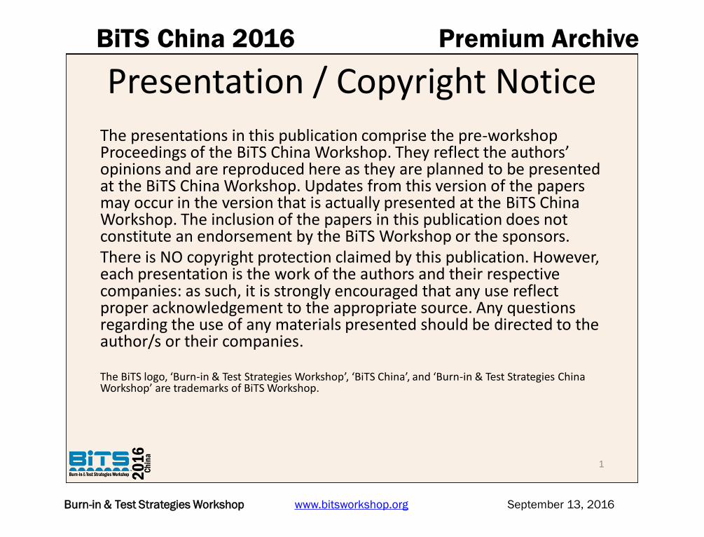
Evolutions in Packaging Technologies for IoT – Assembly and Testing
Yifan Guo
Vice President
Advanced Semiconductor Engineering (ASE)
Keynote
Address BiTS China
BiTS China 2016
September 13, 2016 Burn-in & Test Strategies Workshop www.bitsworkshop.org
Premium Archive
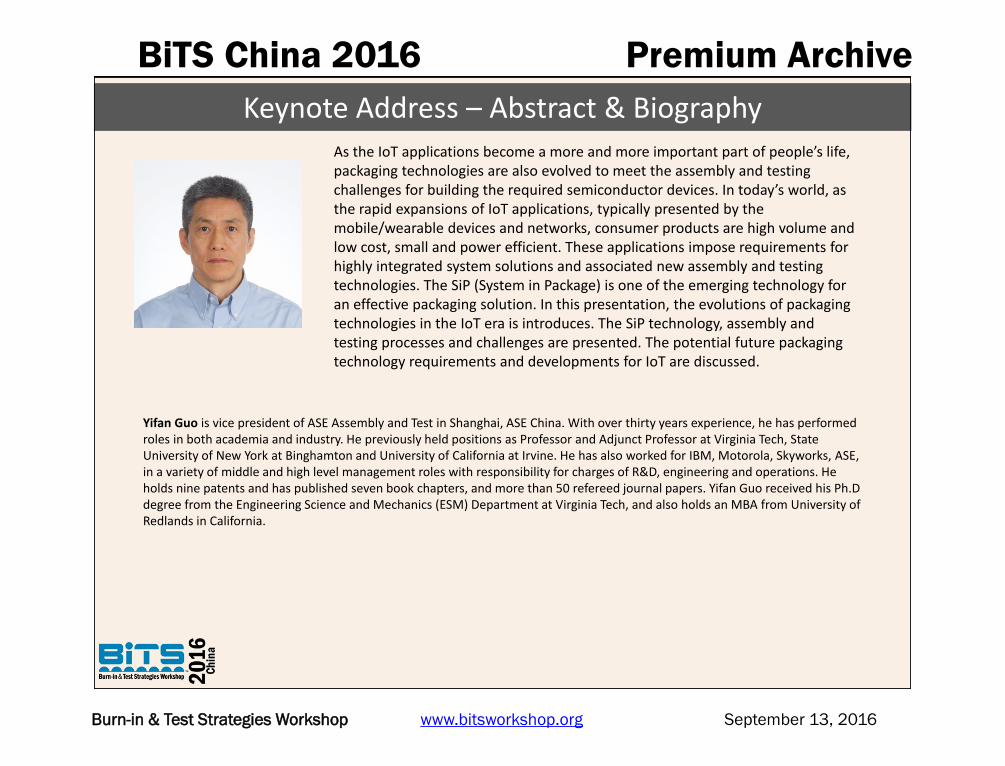
Keynote Address – Abstract & Biography As the IoT applications become a more and more important part of people’s life, packaging technologies are also evolved to meet the assembly and testing challenges for building the required semiconductor devices. In today’s world, as the rapid expansions of IoT applications, typically presented by the mobile/wearable devices and networks, consumer products are high volume and low cost, small and power efficient. These applications impose requirements for highly integrated system solutions and associated new assembly and testing technologies. The SiP (System in Package) is one of the emerging technology for an effective packaging solution. In this presentation, the evolutions of packaging technologies in the IoT era is introduces. The SiP technology, assembly and testing processes and challenges are presented. The potential future packaging technology requirements and developments for IoT are discussed.
Yifan Guo is vice president of ASE Assembly and Test in Shanghai, ASE China. With over thirty years experience, he has performed roles in both academia and industry. He previously held positions as Professor and Adjunct Professor at Virginia Tech, State University of New York at Binghamton and University of California at Irvine. He has also worked for IBM, Motorola, Skyworks, ASE, in a variety of middle and high level management roles with responsibility for charges of R&D, engineering and operations. He holds nine patents and has published seven book chapters, and more than 50 refereed journal papers. Yifan Guo received his Ph.D degree from the Engineering Science and Mechanics (ESM) Department at Virginia Tech, and also holds an MBA from University of Redlands in California.
Evolutions in IC Packaging
Technologies for IoT
BiTS China 2016 2016.09.13 Suzhou, China
ASE Group. All rights reserved. BiTS China 2016
《 Agenda 》
Technology and Application Evolution
Major Trends in Development and Demand
Status and Challenges to Semiconductor A&T
Summary
2
ASE Group. All rights reserved. BiTS China 2016
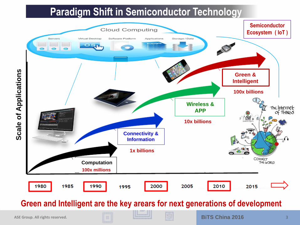
Connectivity & Information
S
cale
of
Ap
plicati
on
s
10x billions
Wireless &
APP
• Smart interfaces
• Sensors
• Networking devices
Computation
Green &
Intelligent
100x billions
1x billions
100x millions
Semiconductor
Ecosystem ( IoT )
Green and Intelligent are the key arears for next generations of development
Paradigm Shift in Semiconductor Technology
3
ASE Group. All rights reserved. BiTS China 2016
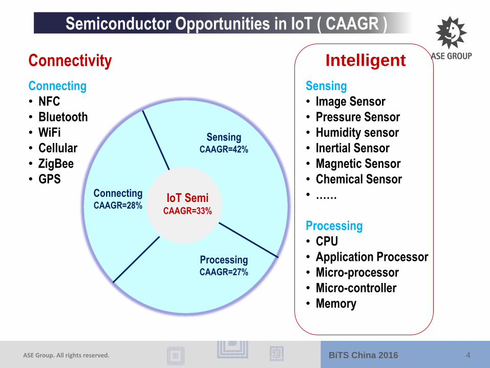
Connecting CAAGR=28%
Sensing CAAGR=42%
Processing CAAGR=27%
Connectivity Intelligent
Semiconductor Opportunities in IoT ( CAAGR )
IoT Semi CAAGR=33%
Connecting
• NFC
• Bluetooth
• WiFi
• Cellular
• ZigBee
• GPS
Sensing
• Image Sensor
• Pressure Sensor
• Humidity sensor
• Inertial Sensor
• Magnetic Sensor
• Chemical Sensor
• ……
Processing
• CPU
• Application Processor
• Micro-processor
• Micro-controller
• Memory
4
ASE Group. All rights reserved. BiTS China 2016
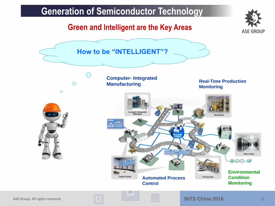
Green and Intelligent are the Key Areas
Generation of Semiconductor Technology
How to be “INTELLIGENT”?
Automated Process
Control
Real-Time Production
Monitoring
Computer- Integrated
Manufacturing
Environmental
Condition
Monitoring
5
ASE Group. All rights reserved. BiTS China 2016
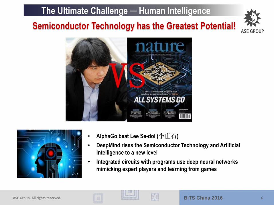
• AlphaGo beat Lee Se-dol (李世石)
• DeepMind rises the Semiconductor Technology and Artificial
Intelligence to a new level
• Integrated circuits with programs use deep neural networks
mimicking expert players and learning from games
The Ultimate Challenge ─ Human Intelligence
Semiconductor Technology has the Greatest Potential!
6
ASE Group. All rights reserved. BiTS China 2016
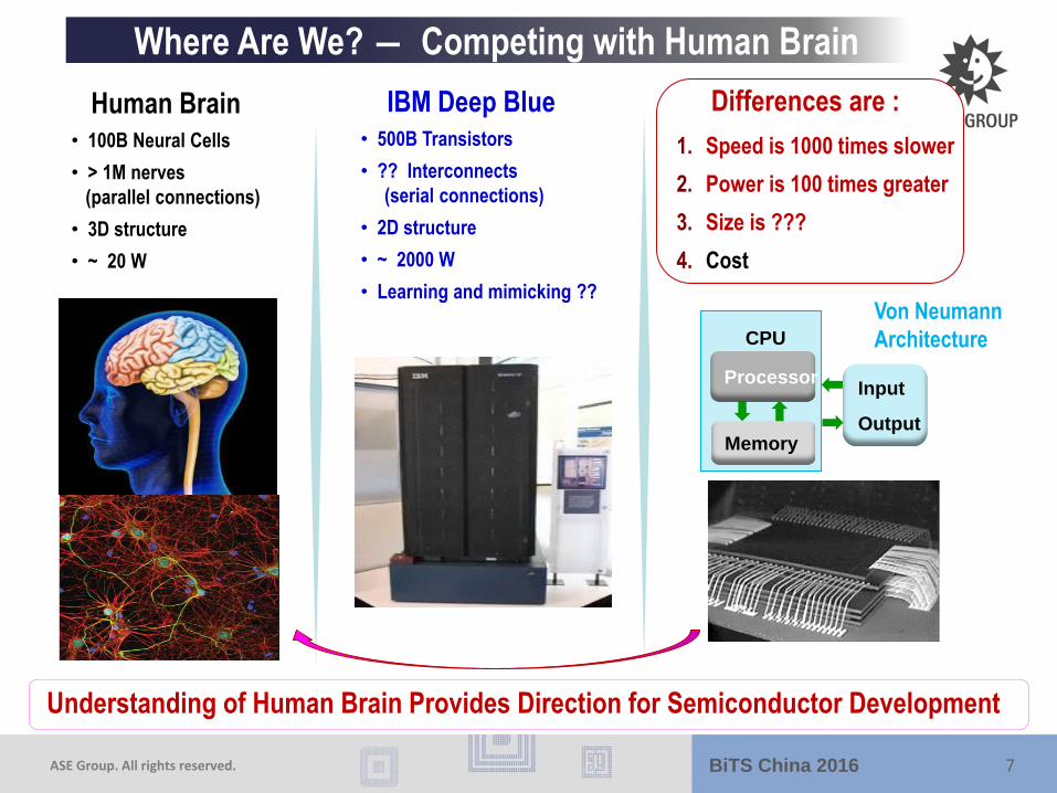
1. Speed is 1000 times slower
2. Power is 100 times greater
3. Size is ???
4. Cost
Human Brain • 100B Neural Cells
• > 1M nerves
(parallel connections)
• 3D structure
• ~ 20 W
IBM Deep Blue • 500B Transistors
• ?? Interconnects
(serial connections)
• 2D structure
• ~ 2000 W
• Learning and mimicking ??
Differences are :
Input
Output
Processor
Memory
Von Neumann
Architecture CPU
Understanding of Human Brain Provides Direction for Semiconductor Development
Where Are We? ― Competing with Human Brain
7
ASE Group. All rights reserved. BiTS China 2016
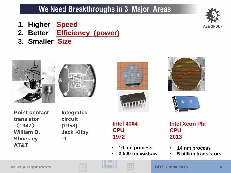
Point-contact
transistor
(1947)
William B.
Shockley
AT&T
Integrated
circuit
(1958)
Jack Kilby
TI
• 14 nm process
• 5 billion transistors
Intel Xeon Phi
CPU
2013
Intel 4004
CPU
1972
• 10 um process
• 2,500 transistors
We Need Breakthroughs in 3 Major Areas
1. Higher Speed
2. Better Efficiency (power)
3. Smaller Size
8
ASE Group. All rights reserved. BiTS China 2016
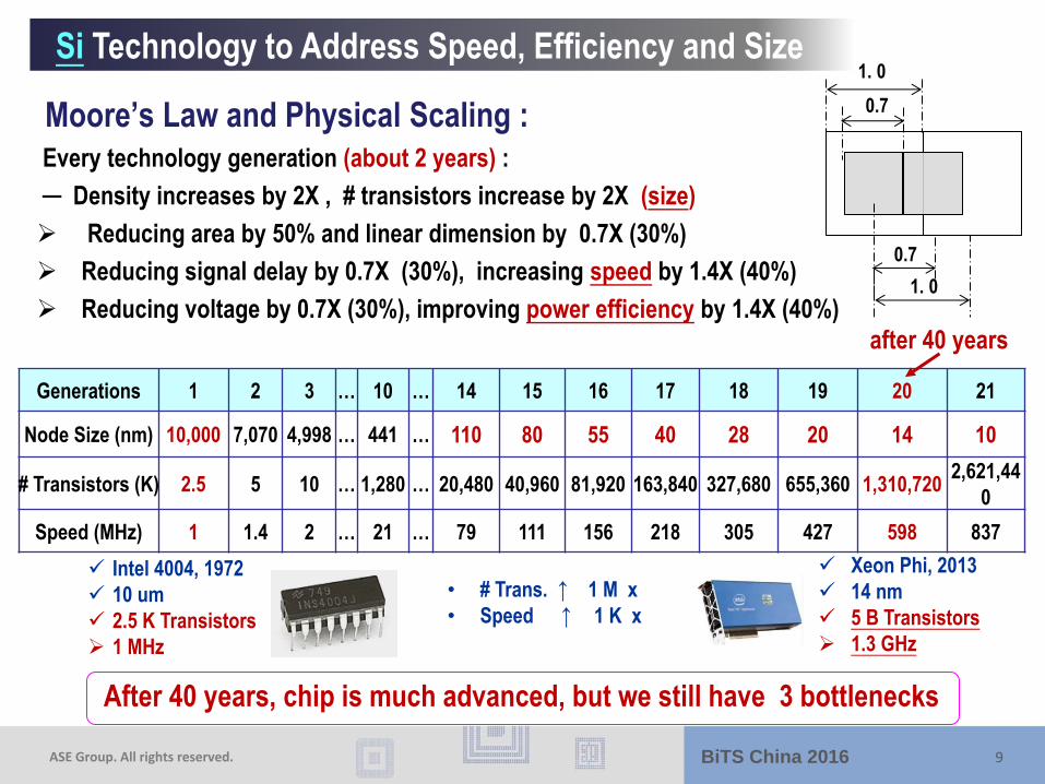
Every technology generation (about 2 years) :
─ Density increases by 2X , # transistors increase by 2X (size)
Reducing area by 50% and linear dimension by 0.7X (30%)
Reducing signal delay by 0.7X (30%), increasing speed by 1.4X (40%)
Reducing voltage by 0.7X (30%), improving power efficiency by 1.4X (40%)
Moore’s Law and Physical Scaling :
Generations 1 2 3 … 10 … 14 15 16 17 18 19 20 21
Node Size (nm) 10,000 7,070 4,998 … 441 … 110 80 55 40 28 20 14 10
# Transistors (K) 2.5 5 10 … 1,280 … 20,480 40,960 81,920 163,840 327,680 655,360 1,310,720 2,621,44
0
Speed (MHz) 1 1.4 2 … 21 … 79 111 156 218 305 427 598 837
after 40 years
1. 0
0.7
Intel 4004, 1972
10 um
2.5 K Transistors
1 MHz
Xeon Phi, 2013
14 nm
5 B Transistors
1.3 GHz
• # Trans. ↑ 1 M x
• Speed ↑ 1 K x
1. 0
0.7
Si Technology to Address Speed, Efficiency and Size
After 40 years, chip is much advanced, but we still have 3 bottlenecks
9
ASE Group. All rights reserved. BiTS China 2016
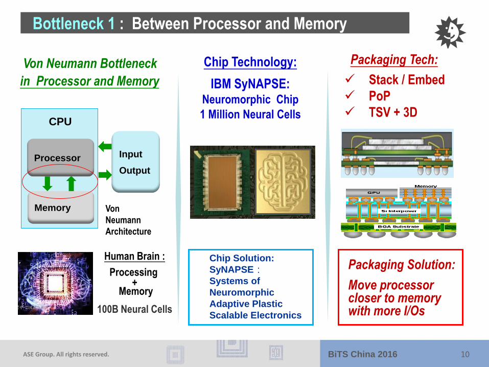
Chip Technology:
IBM SyNAPSE: Neuromorphic Chip
1 Million Neural Cells
Human Brain :
Processing +
Memory
100B Neural Cells
Packaging Tech:
Stack / Embed
PoP
TSV + 3D
Packaging Solution:
Move processor closer to memory with more I/Os
Von Neumann Bottleneck
in Processor and Memory
Chip Solution:
SyNAPSE:
Systems of
Neuromorphic
Adaptive Plastic
Scalable Electronics
Input
Output
Processor
Memory Von
Neumann
Architecture
CPU
Bottleneck 1 : Between Processor and Memory
10
ASE Group. All rights reserved. BiTS China 2016
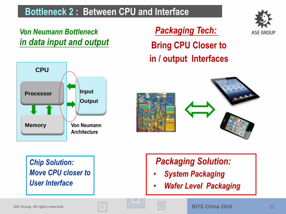
Bring CPU Closer to
in / output Interfaces
Von Neumann Bottleneck
in data input and output
Packaging Solution:
• System Packaging
• Wafer Level Packaging
Packaging Tech:
Input
Output
Processor
Memory Von Neumann
Architecture
CPU
Chip Solution:
Move CPU closer to
User Interface
Bottleneck 2 : Between CPU and Interface
11
ASE Group. All rights reserved. BiTS China 2016
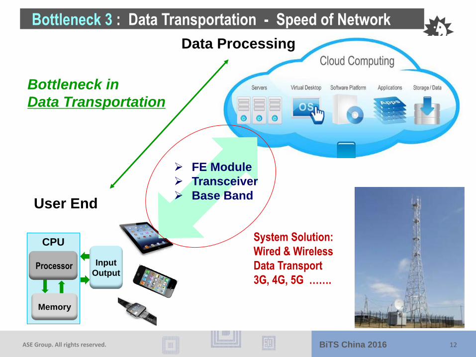
Input
Output Processor
Memory
CPU
FE Module
Transceiver
Base Band
Bottleneck 3 : Data Transportation - Speed of Network
System Solution:
Wired & Wireless
Data Transport
3G, 4G, 5G …….
Bottleneck in
Data Transportation
Data Processing
User End
12
ASE Group. All rights reserved. BiTS China 2016
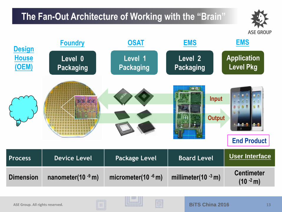
Level 0
Packaging
Foundry
Level 1
Packaging
OSAT
Level 2
Packaging
EMS
Application
Level Pkg
Process Device Level Package Level Board Level User Interface
Dimension nanometer(10 -9 m) micrometer(10 -6 m) millimeter(10 -3 m) Centimeter
(10 -2 m)
Input
Output
Design
House
(OEM)
User Interface
The Fan-Out Architecture of Working with the “Brain”
EMS
13
End Product
ASE Group. All rights reserved. BiTS China 2016
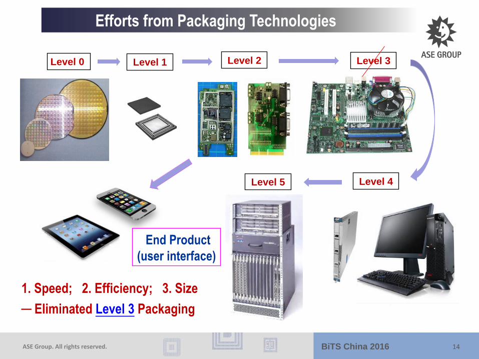
Level 1 Level 2 Level 0
Level 4
Level 3
Level 5
Efforts from Packaging Technologies
1. Speed; 2. Efficiency; 3. Size
─ Eliminated Level 3 Packaging
End Product
(user interface)
14
ASE Group. All rights reserved. BiTS China 2016
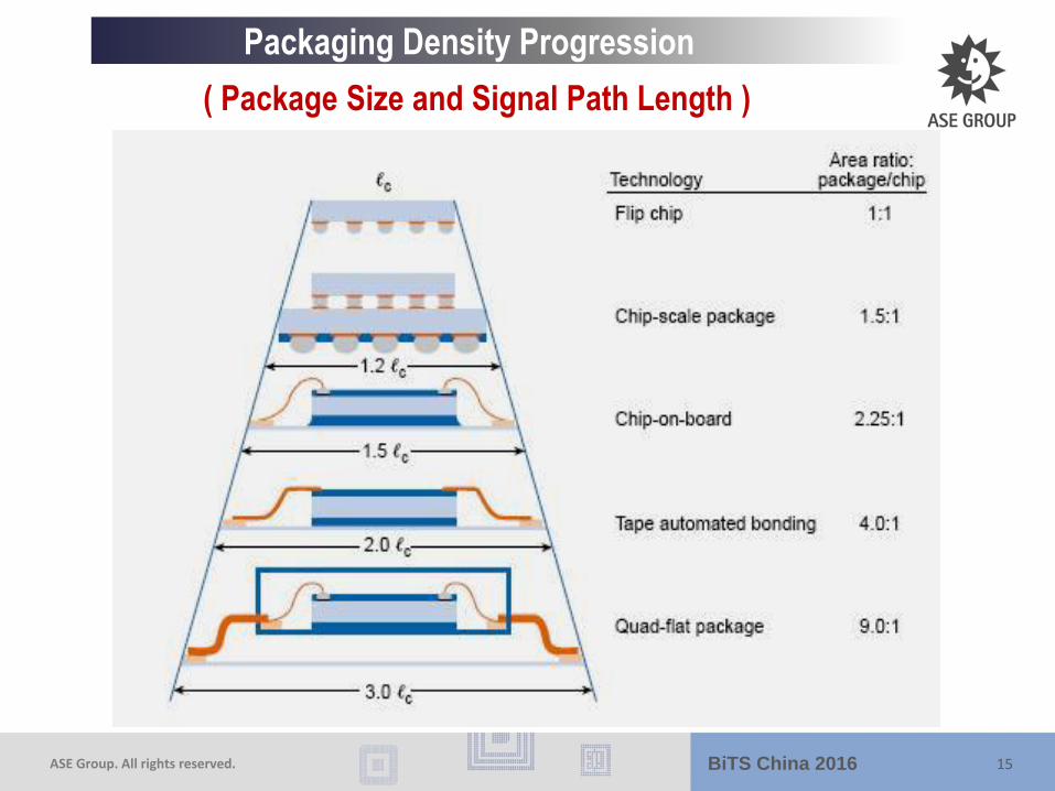
( Package Size and Signal Path Length )
Packaging Density Progression
15
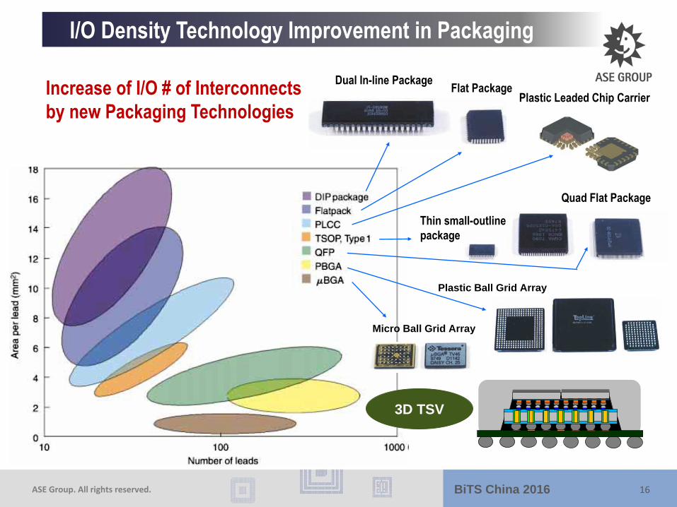
ASE Group. All rights reserved. BiTS China 2016
Thin small-outline
package
Quad Flat Package
Plastic Leaded Chip Carrier
Dual In-line Package
Plastic Ball Grid Array
Micro Ball Grid Array
Flat Package
3D TSV
Increase of I/O # of Interconnects
by new Packaging Technologies
I/O Density Technology Improvement in Packaging
16
ASE Group. All rights reserved. BiTS China 2016
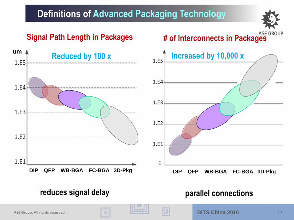
parallel connections reduces signal delay
# of Interconnects in Packages Signal Path Length in Packages
Definitions of Advanced Packaging Technology
DIP QFP WB-BGA FC-BGA 3D-Pkg
Reduced by 100 x um
DIP QFP WB-BGA FC-BGA 3D-Pkg
Increased by 10,000 x
17
ASE Group. All rights reserved. BiTS China 2016
3D and SiP High Density Technology Development
Heterogeneous
Integration
3D TSV SiP
3D FOWLP
2.5 D Interposer
Embedded die
Substrate
DRAM DRAM DRAM DRAM
High Density
Interconnects
18
ASE Group. All rights reserved. BiTS China 2016
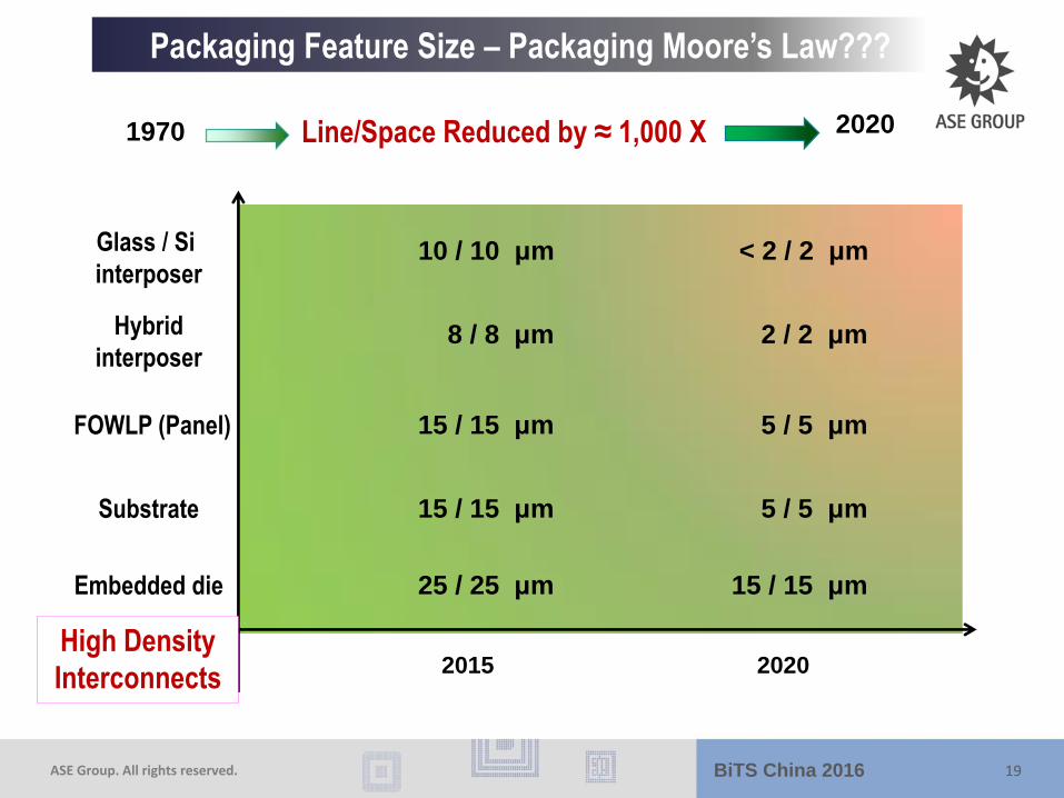
Packaging Feature Size – Packaging Moore’s Law???
Line/Space Reduced by ≈ 1,000 X 1970 2020
2015 2020
Glass / Si
interposer
Hybrid
interposer
FOWLP (Panel)
Substrate
Embedded die
10 / 10 μm < 2 / 2 μm
15 / 15 μm 5 / 5 μm
15 / 15 μm 5 / 5 μm
25 / 25 μm 15 / 15 μm
8 / 8 μm 2 / 2 μm
High Density
Interconnects
19
ASE Group. All rights reserved. BiTS China 2016
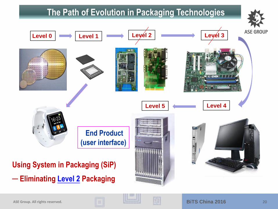
Level 1 Level 2 Level 0
Level 4
Level 3
Level 5
Using System in Packaging (SiP)
─ Eliminating Level 2 Packaging
The Path of Evolution in Packaging Technologies
20
End Product
(user interface)
ASE Group. All rights reserved. BiTS China 2016
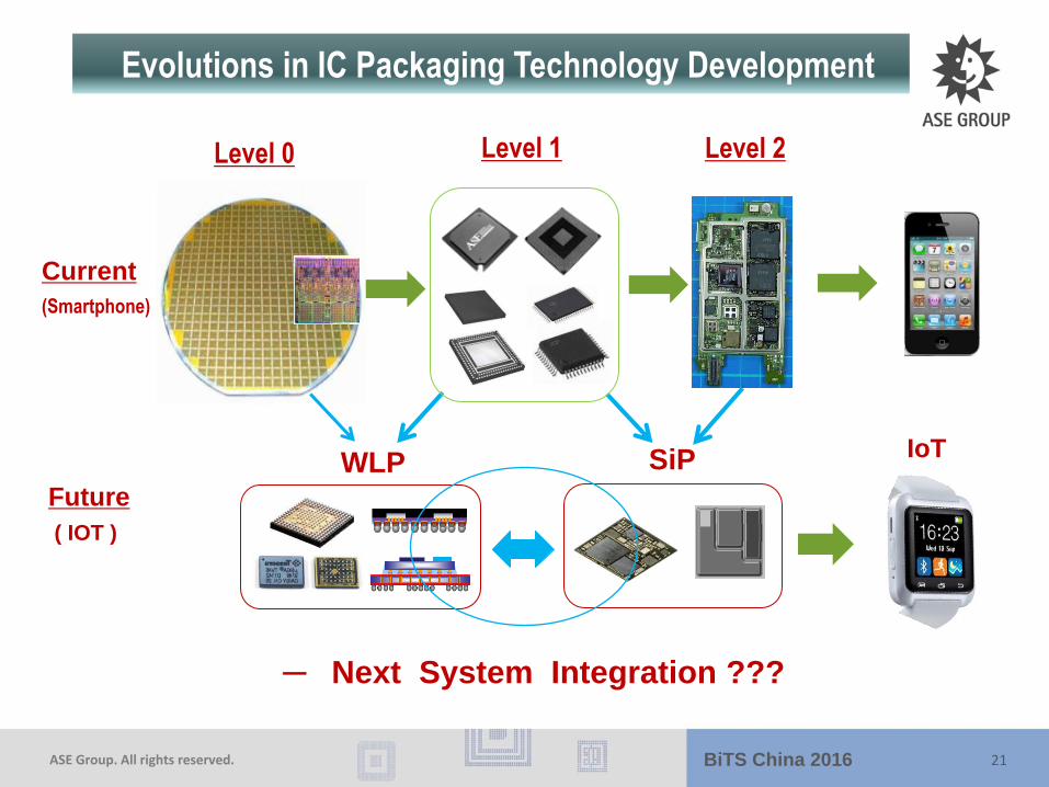
Level 0 Level 1 Level 2
Current
(Smartphone)
Future
( IOT )
WLP SiP IoT
─ Next System Integration ???
Evolutions in IC Packaging Technology Development
21
ASE Group. All rights reserved. BiTS China 2016
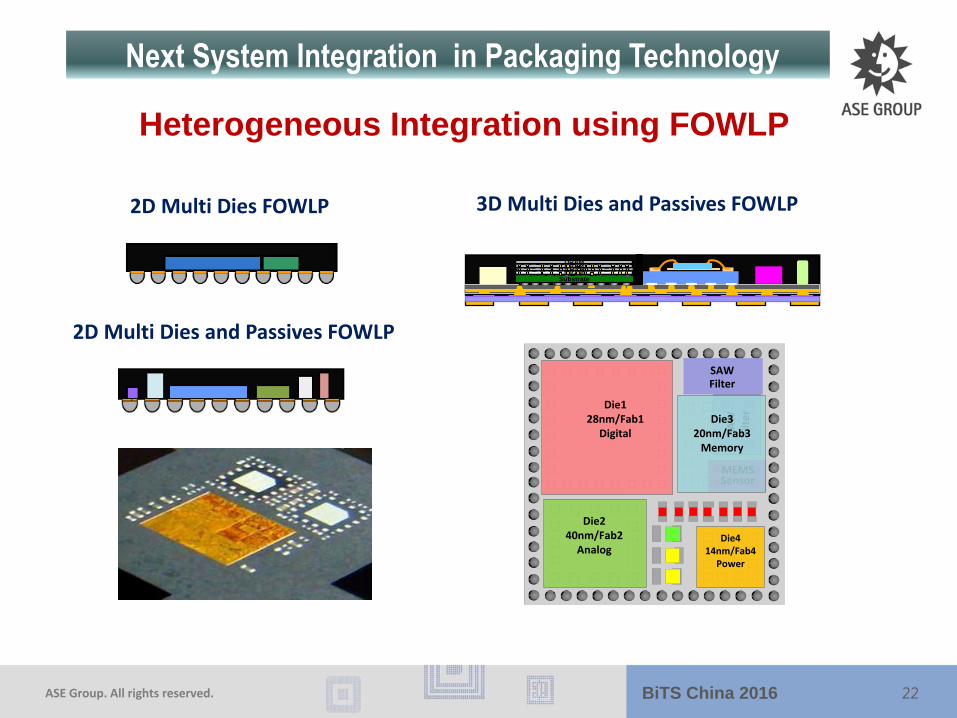
2D Multi Dies FOWLP
2D Multi Dies and Passives FOWLP
Die1 28nm/Fab1
Digital
Die2 40nm/Fab2
Analog Die4
14nm/Fab4 Power
SAW
Fi
lte
r
MEMS Sensor
Die3 20nm/Fab3
Memory
SAW Filter
Heterogeneous Integration using FOWLP
Next System Integration in Packaging Technology
22
3D Multi Dies and Passives FOWLP
Substrate DRAM DRAM DRAM DRAM
ASE Group. All rights reserved. BiTS China 2016
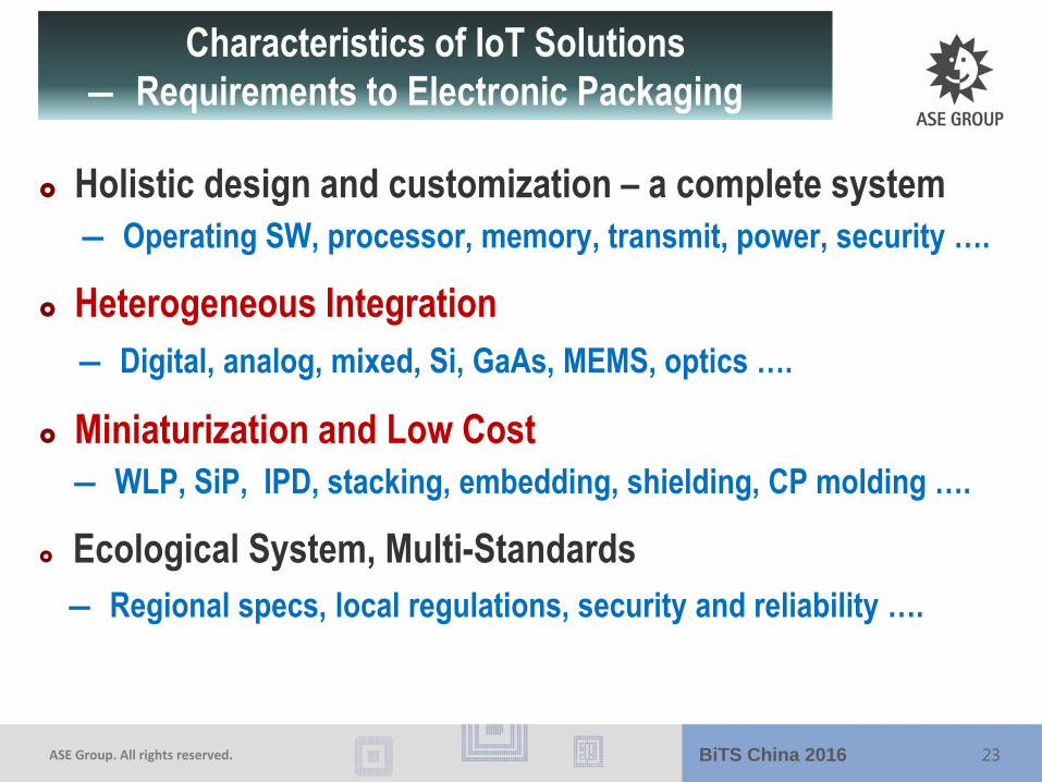
Holistic design and customization – a complete system
― Operating SW, processor, memory, transmit, power, security ….
Heterogeneous Integration
― Digital, analog, mixed, Si, GaAs, MEMS, optics ….
Miniaturization and Low Cost
― WLP, SiP, IPD, stacking, embedding, shielding, CP molding ….
Ecological System, Multi-Standards
― Regional specs, local regulations, security and reliability ….
Characteristics of IoT Solutions
― Requirements to Electronic Packaging
23
ASE Group. All rights reserved. BiTS China 2016
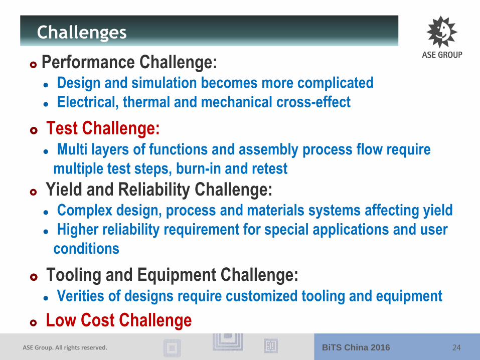
Performance Challenge: Design and simulation becomes more complicated
Electrical, thermal and mechanical cross-effect
Test Challenge: Multi layers of functions and assembly process flow require
multiple test steps, burn-in and retest
Yield and Reliability Challenge: Complex design, process and materials systems affecting yield
Higher reliability requirement for special applications and user
conditions
Tooling and Equipment Challenge: Verities of designs require customized tooling and equipment
Low Cost Challenge
Challenges
24
ASE Group. All rights reserved. BiTS China 2016
A big step toward IoT (wearable) applications
• Integrating Digital, Analog,
RF FEM, PMIC, Memory,
Sensors…
• Employed many state of art
packaging technologies
• Used many new packaging
processes and materials
• Very high density
interconnects and L/S with
many functions
Advanced System in Package ( SiP )
Die1 28nm/Fab1
Digital
Die2 40nm/Fab2
Analog Die4
14nm/Fab4 Power
SAW
Fi
lte
r
MEMS Sensor
Die3 20nm/Fab3
Memory
SAW Filter
25
ASE Group. All rights reserved. BiTS China 2016
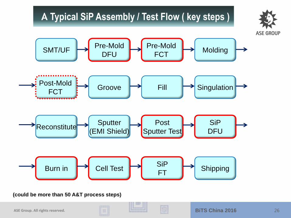
SMT/UF Pre-Mold
DFU
Pre-Mold
FCT Molding
Post-Mold
FCT Groove Fill Singulation
Reconstitute Sputter
(EMI Shield)
Post
Sputter Test
SiP
DFU
Burn in Cell Test SiP
FT
(could be more than 50 A&T process steps)
Shipping
A Typical SiP Assembly / Test Flow ( key steps )
26
ASE Group. All rights reserved. BiTS China 2016
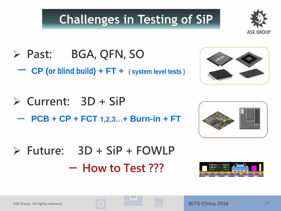
Past: BGA, QFN, SO
─ CP (or blind build) + FT + ( system level tests )
Current: 3D + SiP
─ PCB + CP + FCT 1,2,3…+ Burn-in + FT
Future: 3D + SiP + FOWLP
─ How to Test ???
Substrate DRAM DRAM DRAM DRAM
Challenges in Testing of SiP
27
ASE Group. All rights reserved. BiTS China 2016
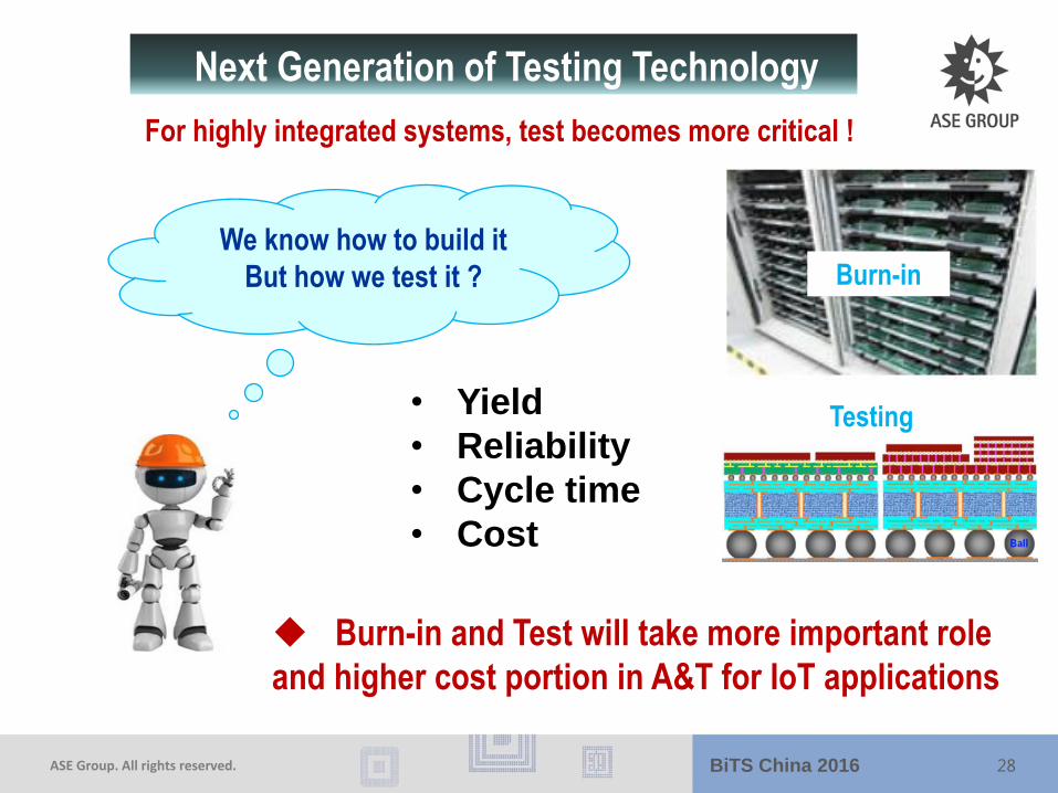
Burn-in and Test will take more important role
and higher cost portion in A&T for IoT applications
• Yield
• Reliability
• Cycle time
• Cost
For highly integrated systems, test becomes more critical !
Burn-in
Next Generation of Testing Technology
We know how to build it
But how we test it ?
Testing
28

www.aseglobal.com
Thank You