Embed Size (px)
Citation preview


Series EditorAnantha Chandrakasan, Massachusetts Institute of TechnologyCambridge, Massachusetts
For other titles published in this series, go to
Integrated Circuits and Systems
www.springer.com/series/7236

Low-Power Crystal andMEMS Oscillators
Eric Vittoz
The Experience of Watch Developments

Eric Vittoz
1015 Lausanne Switzerland
ISSN 1558-9412 ISBN 978-90-481-9394-3 e-ISBN 978-90-481-9395-0 DOI 10.1007/978-90-481-9395-0 Springer Dordrecht Heidelberg London New York
Cover design: Spi Publisher Services Printed on acid-free paper Springer is part of Springer Science+Business Media (www.springer.com)
No part of this work may be reproduced, stored in a retrieval system, or transmitted in any form or by any means, electronic, mechanical, photocopying, microfilming, recording or otherwise, without written permission from the Publisher, with the exception of any material supplied specifically for the purpose of being entered and executed on a computer system, for exclusive use by the purchaser of the work.
© Springer Science+Business Media B.V. 2010
Library of Congress Control Number: 2010930852
Ecole Polytechnique Fédérale de Lausanne (EPFL)

To my wife Monique

Contents
Preface . . . . . . . . . . . . . . . . . . . . . . . . . . . . . . . . . . . . . . . . . . . . . . . . . . . . . . xi
Symbols . . . . . . . . . . . . . . . . . . . . . . . . . . . . . . . . . . . . . . . . . . . . . . . . . . . . . xiii
1 Introduction . . . . . . . . . . . . . . . . . . . . . . . . . . . . . . . . . . . . . . . . . . . . . 11.1 Applications of Quartz Crystal Oscillators . . . . . . . . . . . . . . . . . 11.2 Historical Notes . . . . . . . . . . . . . . . . . . . . . . . . . . . . . . . . . . . . . . 21.3 The Book Structure . . . . . . . . . . . . . . . . . . . . . . . . . . . . . . . . . . . . 21.4 Basics on Oscillators . . . . . . . . . . . . . . . . . . . . . . . . . . . . . . . . . . 4
2 Quartz and MEM Resonators . . . . . . . . . . . . . . . . . . . . . . . . . . . . . . 72.1 The Quartz Resonator . . . . . . . . . . . . . . . . . . . . . . . . . . . . . . . . . . 72.2 Equivalent Circuit . . . . . . . . . . . . . . . . . . . . . . . . . . . . . . . . . . . . . 82.3 Figure of Merit . . . . . . . . . . . . . . . . . . . . . . . . . . . . . . . . . . . . . . . 102.4 Mechanical Energy and Power Dissipation . . . . . . . . . . . . . . . . 152.5 Various Types of Quartz Resonators . . . . . . . . . . . . . . . . . . . . . . 152.6 MEM Resonators . . . . . . . . . . . . . . . . . . . . . . . . . . . . . . . . . . . . . 18
2.6.1 Basic Generic Structure . . . . . . . . . . . . . . . . . . . . . . . . . . 182.6.2 Symmetrical Transducers . . . . . . . . . . . . . . . . . . . . . . . . . 21
3 General Theory of High-Q Oscillators . . . . . . . . . . . . . . . . . . . . . . 233.1 General Form of the Oscillator . . . . . . . . . . . . . . . . . . . . . . . . . . 233.2 Stable Oscillation . . . . . . . . . . . . . . . . . . . . . . . . . . . . . . . . . . . . . 253.3 Critical Condition for Oscillation and Linear Approximation . 273.4 Amplitude Limitation . . . . . . . . . . . . . . . . . . . . . . . . . . . . . . . . . . 273.5 Start-up of Oscillation . . . . . . . . . . . . . . . . . . . . . . . . . . . . . . . . . 293.6 Duality . . . . . . . . . . . . . . . . . . . . . . . . . . . . . . . . . . . . . . . . . . . . . . 303.7 Basic Considerations on Phase Noise . . . . . . . . . . . . . . . . . . . . . 31
3.7.1 Linear Circuit . . . . . . . . . . . . . . . . . . . . . . . . . . . . . . . . . . 31
vii

viii Contents
3.7.2 Nonlinear Time Variant Circuit . . . . . . . . . . . . . . . . . . . 333.8 Model of the MOS Transistor . . . . . . . . . . . . . . . . . . . . . . . . . . . 36
4 Theory of the Pierce Oscillator . . . . . . . . . . . . . . . . . . . . . . . . . . . . . 414.1 Basic Circuit . . . . . . . . . . . . . . . . . . . . . . . . . . . . . . . . . . . . . . . . . 414.2 Linear Analysis . . . . . . . . . . . . . . . . . . . . . . . . . . . . . . . . . . . . . . . 42
4.2.1 Linearized Circuit . . . . . . . . . . . . . . . . . . . . . . . . . . . . . . . 424.2.2 Lossless Circuit . . . . . . . . . . . . . . . . . . . . . . . . . . . . . . . . . 464.2.3 Phase Stability . . . . . . . . . . . . . . . . . . . . . . . . . . . . . . . . . . 504.2.4 Relative Oscillator Voltages . . . . . . . . . . . . . . . . . . . . . . . 514.2.5 Effect of Losses . . . . . . . . . . . . . . . . . . . . . . . . . . . . . . . . . 524.2.6 Frequency Adjustment . . . . . . . . . . . . . . . . . . . . . . . . . . . 54
4.3 Nonlinear Analysis . . . . . . . . . . . . . . . . . . . . . . . . . . . . . . . . . . . . 554.3.1 Numerical Example . . . . . . . . . . . . . . . . . . . . . . . . . . . . . 554.3.2 Distortion of the Gate Voltage . . . . . . . . . . . . . . . . . . . . . 574.3.3 Amplitude Limitation by the Transistor Transfer
Function . . . . . . . . . . . . . . . . . . . . . . . . . . . . . . . . . . . . . . . 584.3.4 Energy and Power of Mechanical Oscillation . . . . . . . . 684.3.5 Frequency Stability . . . . . . . . . . . . . . . . . . . . . . . . . . . . . . 694.3.6 Elimination of Unwanted Modes . . . . . . . . . . . . . . . . . . . 71
4.4 Phase Noise . . . . . . . . . . . . . . . . . . . . . . . . . . . . . . . . . . . . . . . . . . 774.4.1 Linear Effects on Phase Noise . . . . . . . . . . . . . . . . . . . . . 774.4.2 Phase Noise in the Nonlinear Time Variant Circuit . . . . 78
4.5 Design Process . . . . . . . . . . . . . . . . . . . . . . . . . . . . . . . . . . . . . . . 844.5.1 Design Steps . . . . . . . . . . . . . . . . . . . . . . . . . . . . . . . . . . . 844.5.2 Design Examples . . . . . . . . . . . . . . . . . . . . . . . . . . . . . . . . 89
5 Implementations of the Pierce Oscillator . . . . . . . . . . . . . . . . . . . . 935.1 Grounded-Source Oscillator . . . . . . . . . . . . . . . . . . . . . . . . . . . . 93
5.1.1 Basic Circuit . . . . . . . . . . . . . . . . . . . . . . . . . . . . . . . . . . . 935.1.2 Dynamic Behavior of Bias . . . . . . . . . . . . . . . . . . . . . . . . 955.1.3 Dynamic Behavior of Oscillation Amplitude . . . . . . . . . 975.1.4 Design Examples . . . . . . . . . . . . . . . . . . . . . . . . . . . . . . . . 1005.1.5 Implementation of the Drain-to-Gate Resistor . . . . . . . . 1025.1.6 Increasing the Maximum Amplitude . . . . . . . . . . . . . . . . 106
5.2 Amplitude Regulation . . . . . . . . . . . . . . . . . . . . . . . . . . . . . . . . . 1075.2.1 Introduction . . . . . . . . . . . . . . . . . . . . . . . . . . . . . . . . . . . . 1075.2.2 Basic Regulator . . . . . . . . . . . . . . . . . . . . . . . . . . . . . . . . . 1085.2.3 Amplitude Regulating Loop . . . . . . . . . . . . . . . . . . . . . . . 1155.2.4 Simplified Regulator Using Linear Resistors . . . . . . . . . 118

Low-Power Crystal and MEMS Oscillators ix
5.2.5 Elimination of Resistors . . . . . . . . . . . . . . . . . . . . . . . . . . 1205.3 Extraction of the Oscillatory Signal . . . . . . . . . . . . . . . . . . . . . . 1235.4 CMOS-Inverter Oscillator . . . . . . . . . . . . . . . . . . . . . . . . . . . . . . 124
5.4.1 Direct Implementation . . . . . . . . . . . . . . . . . . . . . . . . . . . 1245.4.2 Current-controlled CMOS-inverter oscillator . . . . . . . . . 129
5.5 Grounded-Drain Oscillator . . . . . . . . . . . . . . . . . . . . . . . . . . . . . 1325.5.1 Basic Implementation . . . . . . . . . . . . . . . . . . . . . . . . . . . . 1325.5.2 Single-Substrate Implementation . . . . . . . . . . . . . . . . . . 133
6 Alternative Architectures . . . . . . . . . . . . . . . . . . . . . . . . . . . . . . . . . . 1376.1 Introduction . . . . . . . . . . . . . . . . . . . . . . . . . . . . . . . . . . . . . . . . . . 1376.2 Symmetrical Oscillator for Parallel Resonance . . . . . . . . . . . . . 137
6.2.1 Basic Structure . . . . . . . . . . . . . . . . . . . . . . . . . . . . . . . . . 1376.2.2 Linear Analysis with the Parallel Resonator . . . . . . . . . 1396.2.3 Linear Analysis with the Series Motional Resonator . . 1406.2.4 Effect of Losses . . . . . . . . . . . . . . . . . . . . . . . . . . . . . . . . . 1436.2.5 Nonlinear Analysis . . . . . . . . . . . . . . . . . . . . . . . . . . . . . . 1446.2.6 Phase Noise . . . . . . . . . . . . . . . . . . . . . . . . . . . . . . . . . . . . 1496.2.7 Practical Implementations . . . . . . . . . . . . . . . . . . . . . . . . 157
6.3 Symmetrical Oscillator for Series Resonance . . . . . . . . . . . . . . 1646.3.1 Basic Structure . . . . . . . . . . . . . . . . . . . . . . . . . . . . . . . . . 1646.3.2 Linear Analysis . . . . . . . . . . . . . . . . . . . . . . . . . . . . . . . . . 1656.3.3 Nonlinear Analysis . . . . . . . . . . . . . . . . . . . . . . . . . . . . . . 1726.3.4 Phase Noise . . . . . . . . . . . . . . . . . . . . . . . . . . . . . . . . . . . . 1776.3.5 Practical Implementation . . . . . . . . . . . . . . . . . . . . . . . . . 183
6.4 Van den Homberg Oscillator . . . . . . . . . . . . . . . . . . . . . . . . . . . . 1906.4.1 Principle and Linear Analysis . . . . . . . . . . . . . . . . . . . . . 1906.4.2 Practical Implementation and Nonlinear Behavior . . . . 193
6.5 Comparison of Oscillators . . . . . . . . . . . . . . . . . . . . . . . . . . . . . . 1946.5.1 Pierce Oscillator (1) . . . . . . . . . . . . . . . . . . . . . . . . . . . . . 1956.5.2 Van den Homberg Oscillator (2) . . . . . . . . . . . . . . . . . . . 1966.5.3 Parallel Resonance Oscillator (3) . . . . . . . . . . . . . . . . . . 1966.5.4 Series Resonance Oscillator (4) . . . . . . . . . . . . . . . . . . . . 197
Bibliography . . . . . . . . . . . . . . . . . . . . . . . . . . . . . . . . . . . . . . . . . . . . . . . . . 201
Index . . . . . . . . . . . . . . . . . . . . . . . . . . . . . . . . . . . . . . . . . . . . . . . . . . . . . . . 203

Preface
In the early 60s, the watchmaking industry realized that the newly inventedintegrated circuit technology could possibly be applied to develop electronicwristwatches. But it was immediately obvious that the precision and stabilityrequired for the time base could not be obtained by purely electronic means.A mechanical resonator had to be used, combined with a transducer. The fre-quency of the resonator had to be low enough to limit the power consumptionat the microwatt level, but its size had to be compatible with that of the watch.After unsuccessful results with metallic resonators at sonic frequencies, ef-forts were concentrated on reducing the size of a quartz crystal resonator.Several solutions were developed until a standard emerged with a thin tun-ing fork oscillating at 32kHz and fabricated by chemical etching. After firstdevelopments in bipolar technology, CMOS was soon identified as the bestchoice to limit the power consumption of the oscillator and frequency dividerchain below one microwatt. Low-power oscillator circuits were developedand progressively optimized for best frequency stability, which is the mainrequirement for timekeeping applications. More recent applications to port-able communication devices require higher frequencies and a limited levelof phase noise. Micro-electro-mechanical (MEM) resonators have been de-veloped recently. They use piezoelectric or electrostatic transduction and aretherefore electrically similar to a quartz resonator.
The precision and stability of a quartz is several orders of magnitude bet-ter than that of integrated electronic components. Hence, an ideal oscillatorcircuit should just compensate the losses of the resonator to maintain its os-cillation on a desired mode at the desired level, without affecting the fre-quency or the phase of the oscillation. Optimum designs aim at approachingthis ideal case while minimizing the power consumption.
xi

xii Preface
This book includes the experience accumulated along more than 30 yearsby the author and his coworkers. The main part is dedicated to variants ofthe Pierce oscillator most frequently used in timekeeping applications. Otherforms of oscillators that became important for RF applications have beenadded, as well as an analysis of phase noise. The knowledge is formalized inan analytical manner, in order to highlight the effect and the importance ofthe various design parameters. Computer simulations are limited to particularexamples but have been used to crosscheck most of the analytical results.
Many collaborators of CEH (Centre Electronique Hologer, WatchmakersElectronic Center), and later of CSEM, have contributed to the know-howdescribed in this book. Among them, by alphabetic order, Daniel Aebischer,Luc Astier, Serge Bitz, Marc Degrauwe, Christian Enz, Jean Fellrath, ArminFrei, Walter Hammer, Jean Hermann, Vincent von Kaenel, Henri Oguey, andDavid Ruffieux. Special thanks go to Christian Enz for the numerous discus-sions about oscillators and phase noise during the elaboration of this book.
Eric A. VittozCernier, SwitzerlandFebruary 2010

Symbols
Table 0.1 Symbols and their definitions.
Symbol Description Reference
a Power factor of the flicker noise current (6.71)A Normalized transconductance in series resonance oscillator (6.108)B Normalized bandwidth in series resonance oscillator (6.108)Ca, Cb Functional capacitors Fig. 6.37CD Capacitance between drains Fig. 6.1CL Load capacitance in series resonance oscillator Fig. 6.16Cm (Cm,i) Motional capacitance (of mode i) Fig. 2.2CP Total parallel capacitance of the resonator (2.22)Cs Series connection of C1 and C2 (4.9)CS Capacitance between sources Fig. 6.1C0 Parallel capacitance of the dipole resonator (2.1)C1 Total gate-to-source capacitance Fig. 4.1C2 Total drain-to-source capacitance Fig. 4.1C3 Total capacitance across the motional impedance Fig. 2.2Em Energy of mechanical oscillation (2.23)f Frequencyfm Motional resonant frequency (4.140)fs Frequency of stable oscillation (3.24)fs(mv) Fundamental function in strong inversion (6.37)fw(vin) Fundamental function in weak inversion (6.30)Fa Flicker noise current constant (6.71)Ga Reference conductance for the flicker noise current (6.71)Gds Residual output conductance in saturation (3.57)Gm Gate transconductance of a transistor (3.53)
continued on next page
xiii

xiv Symbols
continued from previous page
Symbol Description ReferenceGms Source transconductance of a transistor (3.49)Gmd Drain transconductance of a transistor (3.49)Gmcrit Critical transconductance for oscillation Fig. 4.4Gmcrit0 Critical transconductance for lossless circuit Fig. 4.6Gmlim Limit transconductance in series resonance oscillator (6.109)Gmmax Maximum possible transconductance for oscillation Fig. 4.4Gmopt Optimum value of transconductance Fig. 4.4Gm(1) Transconductance for the fundamental frequency (4.54)
Gvi Transconductance of the regulator (5.52)hs(mi) Transconductance function in strong inversion (6.142)IB0(x) Modified Bessel function of order 0 (4.59)IB1(x) Modified Bessel function of order 1 (4.61)Ic Circuit current Fig. 3.1Ics Value of Ic at stable oscillation (3.6)ID Drain current Fig. 3.10ID0 DC component of drain current (5.1.2)ID(1) Fundamental component of ID Fig. 4.13IF Forward component of drain current (3.40)Im Motional current Fig. 2.2Ims Value of Im at stable oscillation (3.6)IR Reverse component of drain current (3.40)Ispec Specific current of a transistor (3.41)I0 Bias current of the oscillator Fig. 4.13I0start Start-up value of bias current (5.45)I0crit Critical value of bias current I0 Fig. 4.14I0critmin Critical current in weak inversion (4.64)I1 Complex value of the sinusoidal drain current 6.3.2.3IC Inversion coefficient of a transistor (3.45)IC0 Inversion coefficient at I0 = I0crit (4.72)kc Capacitive attenuation factor (4.69)Kf Flicker noise voltage constant of a transistor (3.62)Kf i Flicker noise current function (3.36)Kf v Flicker noise voltage function (3.35)Kg Transconductance ratio Fig. 6.37Ki Mirror ratio in the regulator Fig. 5.9Kiv Gain parameter of |V1|(ID0) (5.24)Kl Level of specific current (6.92)Km Margin factor (4.17)Kr Ratio of transfer parameters Fig. 5.4
continued on next page
Low-Power Crystal and MEMS Oscillators xv
continued from previous page
Symbol Description ReferenceKs Ratio of specific currents (6.82)Kt Transconductance ratio (6.175)Kw Width ratio in the regulator (5.43)Lm (Lm,i) Motional inductance (of mode i) Fig. 2.2mi Index of current modulation (6.133)mv Index of voltage modulation (4.122)mvd Index of voltage modulation for a differential pair (6.35)M Figure of merit (2.9)MD Figure of merit of the resonator used as a dipole (2.22)ML Figure of merit of the resonator used as a loaded dipole (6.7)M0 Intrinsic figure of merit of the resonator (2.10)n Slope factor of a transistor (3.40)p Frequency pulling (2.7)pc Frequency pulling at critical condition for oscillation (3.10)ppa Frequency pulling at parallel resonance (2.15)ps Frequency pulling at stable oscillation (3.7)pse Frequency pulling at series resonance (2.14)Pm Power dissipated in the resonator (2.24)Q (Qi) Quality factor (of mode i) (2.3)Qb Quality factor of the bias circuit (5.12)Riv Slope of the amplitude |V1|(I0) Fig. 5.3RL Load resistance Fig. 6.16Rm (Rm,i ) Motional resistance (of mode i) Fig. 2.2Rn Negative resistance of the circuit (3.2)Rn0 Value of Rn for the linear circuit (3.12)svi Normalized slope of the regulator Fig. 5.10siv Normalized slope of the amplitude Fig. 4.17S
I2n
Current noise spectrum (4.107)
SI2nD
Drain current channel noise spectrum (3.59)
SI2nL
Loop Current noise spectrum (3.27)
SV 2
nVoltage noise spectrum (4.107)
SV 2
nGGate voltage flicker noise spectrum (3.62)
Sφ 2n
Phase noise power spectrum (3.29)
t TimeUT Thermodynamic voltage (3.40)V Voltage across the resonator Fig. 2.2VB Supply voltage (battery voltage) Fig. 5.1vc Value of |Vc| normalized to nUT (6.130)Vc Control voltage of a transistor (6.129)
continued on next page

xvi Symbols
continued from previous page
Symbol Description ReferenceVD Drain voltage Fig. 3.10VDsat Saturation value of drain voltage (3.46)ve Normalized effective DC gate voltage (4.57)VG Gate voltage Fig. 3.10VG0 DC component of gate voltage (4.52)vin Value of |Vin| normalized to nUT (6.31)Vin Differential input voltage Fig. 6.5VM Channel length modulation voltage (3.57)Vn Open-loop noise voltage of the circuit 3.7.1VS Source voltage Fig. 3.10VT 0 Threshold voltage of a transistor (3.40)V(1) Complex value of fundamental component of V (3.1)
v1 value of |V1| normalized to nUT (4.57)V1 Complex value of gate-to-source voltage Fig. 4.8V2 Complex value of drain-to-source voltage Fig. 4.8V3 Complex value of drain-to-gate voltage Fig. 4.8Zc Impedance of the linear circuit (3.8)Zc(1) Circuit impedance for fundamental frequency (3.1)Zc0 Circuit impedance without parallel capacitance (6.3)ZD Impedance between drains Fig. 6.3ZL Load impedance Fig. 6.16Zm (Zm,i) Motional impedance (of mode i) Fig. 2.2Zp Total parallel impedance (2.12)ZS Impedance between sources Fig. 6.3Z1 Total gate-to-source impedance Fig. 4.3Z2 Total drain-to-source impedance Fig. 4.3Z3 Total drain-to-gate impedance Fig. 4.3α Ratio of critical transconductance (4.98)αi Noise current modulation function Fig. 3.9αv Noise voltage modulation function Fig. 3.9α0 Value of α for the lossless case (4.99)β Transfer parameter of a transistor (3.44)∆ω Noise frequency offset (3.28)εmax Maximum relative mismatch (6.15)ε0 Permittivity of free space (2.27)γ Noise excess factor of the oscillator Fig. 3.7γt Channel noise excess factor of a transistor (3.60)Γi Effective impulse sensitivity function for noise current (3.34)Γv Effective impulse sensitivity function for noise voltage (3.32)
continued on next page

Low-Power Crystal and MEMS Oscillators xvii
continued from previous page
Symbol Description Referenceτ Time constant of oscillation growth (3.16)τ0 Start-up value of τ (3.15)ω Approximate angular frequency of oscillationωm (ωm,i) angular frequency of resonance (of mode i) (2.2)ωn Angular frequency at which noise is considered (4.106)ωs Angular frequency at stable oscillation (3.24)Ωciv Cut-off angular frequency of |V1|(ID0) (5.26)Ω0 Resonant angular frequency of bias circuit (5.10)Ω1 Unity gain frequency of the regulation loop (5.71)

Chapter 1Introduction
1.1 Applications of Quartz Crystal Oscillators
Relevant time durations for modern science range from the femtosecond ofvery fast electronics to the age of the universe, 15 billion years. This corres-ponds to a range of about 32 orders of magnitude. Moreover, this variable canbe controlled and measured with an accuracy better than 10−14 by modernatomic clocks. However, the accuracy that can be obtained by purely elec-tronic circuits, such as integrated circuits, is only of the order of 10−3. Thisis because there is no combination of available electronic components (likea RC time constant for example) that is more precise and constant with timeand temperature. Now, 10−3 corresponds to an error of about 1.5 minute perday, which is totally unacceptable for timekeeping applications. The sameis true for applications to modern telecommunications, which exploits thefrequency spectrum up to 300Ghz.
Quartz crystal oscillators offer the range of accuracy required by theseapplications by combining the electronic circuit with a simple electromech-anical resonator that essentially controls the frequency.
Timekeeping devices like wristwatches need a long-term precision betterthan 10−5, possibly 10−6 that corresponds to 30s/year. Additional require-ments for watches include a very low power consumption, of the order of 0.1µW in the range of indoor and outdoor temperatures. The frequency shouldbe as low as possible, to minimize the additional power consumed by thefrequency divider (period counter).
1Integrated Circuits and Systems, DOI 10.1007/978-90-481-9395-0_1, E. Vittoz, Low-Power Crystal and MEMS Oscillators: The Experience of Watch Developments,
© Springer Science+Business Media B.V. 2010

2 1 Introduction
The same level of long-term precision is needed for telecommunications,with less demanding requirements on power consumption. However, higheror much higher frequencies are needed, and there is an additional importantrequirement on phase noise (or short-time stability).
Crystal oscillators are also often used for generating the clock of digitalsystems or analog circuits. The precision needed is then of the order of 10−4,which makes the quartz oscillator very uncritical, but problems may arise ifis is not properly designed, the worst one being oscillation on an parasiticresonance of the resonator.
1.2 Historical Notes
The first quartz crystal oscillator was invented by Walter Guyton Cady in1921 [1], as a way to produce an electrical signal of very constant frequency.Soon after, George Washington Pierce developed a very elegant oscillatorcircuit using a single vacuum tube [2, 3], that has been easily adapted tointegrated circuits, some 40 years later. Quartz oscillators have since beenused extensively to produce the accurate and stable frequency needed for thecarrier of telecommunication circuits.
Artificial quartz, first produced in 1958, progressively replaced naturalquartz crystal. Quartz production was boosted in the seventies by a surge ofdemand for the 40-channel of citizen band transceivers. It was alleviated bythe introduction of frequency synthesizers made possible by the evolution ofVLSI circuits.
The application of quartz oscillators to timekeeping devices started in1927 with the first quartz clock developed by Marrison and Horton [4]. Port-able clocks became possible with the invention of the transistor, but integ-rated circuits were needed to develop the first quartz wristwatch presented in1967 [5].
1.3 The Book Structure
After this short introductory chapter, Chapter 2 is essentially dedicated to thequartz crystal resonator and to its electrical equivalent circuit. By exploit-ing the very large value of quality factor Q, the electrical impedance of theresonator is described by a bilinear function of the relative amount p of fre-quency difference with the mechanical resonant frequency, called frequency

Low-Power Crystal and MEMS Oscillators 3
pulling. After a brief description of the various types of quartz resonators,a last section shows how the equivalent circuit of a MEM resonator usingan electrostatic transducer can be reduced qualitatively to that of the quartzresonator.
Chapter 3 describes a general theory that applies to all oscillators based ona high-Q series resonant circuit (or parallel resonant circuit by swapping cur-rents for voltages). By adequately splitting conceptually the oscillator intoa frequency-independent nonlinear part and a frequency-dependent linearseries resonator, this approach allows to predict the amplitude and the pre-cise value of frequency pulling by including nonlinear effects. This chapteralso introduces some basic considerations on phase noise. An analysis of theeffect of cyclostationary noise sources is proposed, based on the effectiveimpulse sensitivity function (ISF) [6], with the approximation of sinusoidalwaveforms made possible by the high value of Q. The chapter ends with ashort introduction to the EKV analytical model of the MOS transistor that isused in all subsequent circuit analyses.
Chapter 4 concentrates on the theory of the Pierce oscillator [3], which isthe only possible architecture with a single active transistor. The linear ana-lysis (valid at the critical condition for oscillation or for sufficiently smallamplitudes) capitalizes on the circular locus resulting from the bilinear de-pendency of the circuit impedance on the transconductance of the transistor.The amplitude of oscillation is obtained analytically from the DC transferfunction of the transistor, using the fact that the gate voltage remains almostsinusoidal. The important problem of frequency stability and that of avoidingoscillation on a parasitic resonant mode of the resonator are also discussed.Phase noise is then approached analytically, using the concept of effectiveimpulse sensitivity function (ISF) to treat the effect of the cyclostationarywhite and flicker noise produced by the active transistor. A design process ispresented and illustrated by two numerical examples.
Chapter 5 deals with the practical realization of the Pierce oscillator. Thedynamic behavior of the grounded source implementation with respect tovariations of its bias current is analyzed. The oscillator is then embeddedin an amplitude regulating loop based on a particular amplitude regulatorscheme. The results are then applied to the two numerical examples presen-ted in Chapter 4. The Pierce oscillator is frequently realized by means ofa simple CMOS inverter. A qualitative analysis supported by circuit simu-lations demonstrates the many drawbacks of this solution. A better way toreduce the power consumption by means of complementary transistors ispresented. The chapter ends with the grounded-drain implementation, whichhas the advantage of requiring only one pin to connect the external reson-

4 1 Introduction
ator. Its performance is shown to be lower than that of the grounded-sourcesolution, especially if the active transistor is not put in a separate well.
Many architectures become possible when two or more active transistorsare considered. Chapter 6 describes and analyzes three of them. The first oneis a symmetrical circuit that exploits the parallel resonance of the resonator,and delivers symmetrical output voltages [25]. The power consumption ofthis circuit can be made very low, at the cost of an increased sensitivity ofthe frequency to electrical parameters. The second circuit is also symmetricaland based on two active transistors. It produces a current stable DC negativeresistance compatible with a series resonator. Compared to other solutions,the power consumption of this circuit is lower for low-Q resonators and/orfor very low values of frequency pulling. In the third architecture [27], oneside of the resonator is grounded (one-pin oscillator). This more complexcircuit uses a full operational transconductance amplifier (OTA) combinedwith two grounded capacitors. The chapter ends with a comparison of thefour types of oscillators analyzed in the book.
An analytical approach is favored all along the chapters, with a list of allthe variables at the beginning of the book. Results are simple equations illus-trated by normalized graphs. The advantage is to explicit clearly the effectof each design parameter on the circuit performance. The drawback is thatsome approximations are sometimes necessary, leading to approximative res-ults. Computer simulations can then be used to obtain more precision. Mostof the analytical results have been cross-checked by circuit simulations, withthe notable exception of phase noise. Theses simulations have been carriedout with the LTspice circuit simulator of Linear Technology and the EKVmodel of the MOS transistor.
1.4 Basics on Oscillators
As depicted in Fig. 1.1, the most general way of describing an oscillator is bya frequency-dependent nonlinear circuit block connected in closed loop. Thetransfer function of the block is G(ω ,A), where ω is the angular frequencyand A is the input amplitude.
If the circuit is strongly nonlinear with a large bandwidth, it results in arelaxation oscillator, the waveform of which is far from being sinusoidal.
On the contrary, if the circuit has a narrow bandwidth, the system becomesa harmonic oscillator and the oscillatory signal is approximately sinusoidal.Stable oscillation may take place at frequency ωs with an amplitude As for

Low-Power Crystal and MEMS Oscillators 5
ω
Figure 1.1 General representation of an oscillator.
G(ωs,As) = 1. (1.1)
However, this is only possible if two fundamental conditions are fulfilled.The first condition is that for phase stability [7]
d(arg G)dω
|ωs,As< 0. (1.2)
No periodic solution can be maintained if this condition is not fulfilled. Thesecond condition is that of amplitude stability
d|G|dA
|ωs,As< 0. (1.3)
This condition requires that the circuit block contains some nonlinearity tofix the amplitude of oscillation.
Although this approach of a closed loop is applicable to all kinds of os-cillators, we will show in Chapter 3 that, for the case of oscillators includinga resonator with very high quality factor, more insight can be obtained byseparating this resonator from the rest of the circuit.

Chapter 2Quartz and MEM Resonators
2.1 The Quartz Resonator
As illustrated by Fig. 2.1(a), a quartz resonator is essentially a capacitor,the dielectric of which is silicon dioxide (SiO2), the same chemical com-pound as used in integrated circuits. However, instead of being a glass, it is amonocrystal, a quartz crystal, which exhibits piezoelectric properties. There-fore, a part of the electrical energy stored in the capacitor is converted intomechanical energy.
Figure 2.1 Quartz crystal resonator: (a) Schematic structure; (b) symbol.
Whatever the shape of the piece of quartz, it has some mass and someelasticity; it can therefore oscillate mechanically. Unlike simple LC electricalresonators, mechanical resonators always possess several resonance frequen-cies, corresponding to different possible modes of oscillation (eigenmodes).
E. Vittoz, Low-Power Crystal and MEMS Oscillators: The Experience of Watch Developments,Integrated Circuits and Systems, DOI 10.1007/978-90-481-9395-0_2,
7
© Springer Science+Business Media B.V. 2010

8 2 Quartz and MEM Resonators
Now, if an AC voltage is applied to the capacitor at a frequency close tothat of a possible mode, it can possibly excite this mode and drive the quartzresonator into mechanical oscillation.
In addition to its piezoelectric properties, quartz has the advantage of be-ing an excellent mechanical material, with very small internal friction. It hastherefore a very high intrinsic quality factor, of the order of 106.
The resonant frequency depends essentially on the shape and the dimen-sions of the piece of quartz. Possible frequencies range from 1 kHz for largecantilever resonators to hundreds of MHz for very thin thickness-mode res-onators.
The exact frequency and its variation with temperature depend on the ori-entation with respect to the 3 crystal axes. By choosing the optimum modewith an optimum orientation, the linear and quadratic components of thevariation of the frequency with temperature can be cancelled, leaving at besta residual dependency of about 10−6 from -20 to +80C.
2.2 Equivalent Circuit
The equivalent circuit of a quartz resonator is shown in Fig. 2.2(a). Althoughthe intrinsic device is a dipole, it is very important in some circuits to modelit as a 3-point component, in order to separate the electrical capacitor C12from the parasitic capacitances to the packaging case C10 and C20.
If the device is only considered as a dipole, with node 0 floating, then thelumped electrical capacitance is
C0 C12 +C10C20
C10 +C20. (2.1)
Each possible mode of oscillation i of the resonator corresponds to a mo-tional impedance Zm,i formed by the series resonant circuit Rm,iLm,iCm,i. Themotional inductance Lm is proportional to the mass of the mechanical reson-ator. The motional capacitance Cm is proportional to the inverse of its stiff-ness. The motional resistance Rm represents the mechanical losses.
The resonant angular frequency of mode i is given by
ωm,i = 1/√
Lm,iCm,i, (2.2)
and its quality factor by
Qi =1
ωm,iRm,iCm,i=
ωm,iLm,i
Rm,i=
1Rm,i
√Lm,i
Cm,i. (2.3)

Low-Power Crystal and MEMS Oscillators 9
Figure 2.2 Equivalent circuit: (a) of the resonator alone with all possible modes;(b) of a single mode with C12 increased to C3 by external capacitors.
This factor is very large, typically ranging from 104 to 106. Wheneverneeded, this relation between Q, ωm, Rm and Cm will be used implicitlythroughout this book.
The motional current Im,i flowing through the motional impedance Zm,iis proportional to the velocity of mode i. Thus its peak value |Im,i| is pro-portional to the peak velocity and |Im,i|/ωi to the amplitude of oscillation ofmode i.
The voltage V across the motional impedances is proportional to the forceproduced by the piezoelectric effect.
The ratio Cm,i/C12 1 represents the electromechanical coupling to themode i. It is always much lower than unity, since it never exceeds the in-trinsic coupling coefficient of quartz, which is about 1%. If a mode i is notcoupled at all, then Cm,i = 0 and the corresponding branch disappears fromthe equivalent circuit.
At this point, two very important remarks must be introduced, since theywill greatly simplify the nonlinear analysis of quartz oscillators:
1. Since Qi 1, the bandwidth of Zm is very narrow. Hence, for frequen-cies close to the resonance of mode i, the harmonic content of the motionalcurrent Im,i is always negligible. Thus, this current can be considered per-fectly sinusoidal, even if the voltage V is strongly distorted:
Im,i(t) = |Im,i|sin (ωt) (2.4)

10 2 Quartz and MEM Resonators
or, expressed as a complex value
Im,i = |Im,i|exp ( jωt). (2.5)
2. Among the various possible modes of oscillation, we may have the“overtones”, the frequencies of which are close to multiples of that of thefundamental mode. However, because of end effects, these frequencies arenot exact multiples of the fundamental. Hence, once a mode is excited, theharmonics that can be produced by the distortion of V cannot excite theseovertones. Once oscillation has taken place at one mode, the other modes(and thus the other branches in the equivalent circuit) can be ignored.
From now on, let us consider only this particular “wanted” mode, and dropthe index i in the notations. The equivalent circuit is then reduced to that ofFig. 2.2(b), where C3 now includes external capacitances possibly added toC12 of the resonator itself.
The complex motional impedance is given by
Zm = Rm + jωLm +1
jωCm= Rm +
jωCm
· ω + ωm
ωm· ω −ωm
ωm, (2.6)
where the last term has be obtained by introducing (2.2).Now, because of the very large value of Q, the frequency of oscillation
will always be very close to ωm. It is thus very useful to replace ω by therelative amount of frequency pulling (by the circuit)
p ω −ωm
ωmwith |p| 1, (2.7)
which, introduced in (2.6), gives almost exactly
Zm = Rm + j2p
ωCm, (2.8)
where ω can be considered constant with respect to its effect on Zm. Hence,Zm is a linear impedance that is strongly dependent on p. Indeed, its real partis constant (as long as the quality factor remains constant) but its imaginarypart is proportional to p.
2.3 Figure of Merit
An important parameter of quartz resonators (and of all electrostaticallydriven resonators) is its figure of merit

Low-Power Crystal and MEMS Oscillators 11
M 1ωC3Rm
=QCm
C3, (2.9)
which has a maximum intrinsic value when C3 is reduced to its minimumvalue C12, defined as
M0 1ωC12Rm
=QCm
C12. (2.10)
Indeed, M is the maximum possible ratio of currents through Zm and C3. Byintroducing this definition in (2.8), we can express Zm normalized to 1/ωC3as
ωC3Zm =1M
(1+ 2Qp j). (2.11)
We can now calculate Zp, the impedance of the parallel connection of Zm andC3. Assuming ω constant (since p 1), it gives, in normalized form:
ωC3Zp =1+ 2Qp j
(M−2Qp)+ j=
M−[4(Qp)2 −2MQp+ 1
]j
(M−2Qp)2 + 1. (2.12)
This impedance becomes real for
Qp =M±
√M2 −44
. (2.13)
The negative sign correspond to the series resonance frequency, at a valueof pulling
pse =Cm
4C3
[1−
√1−4/M2
], (2.14)
whereas the positive sign corresponds to the parallel resonance frequency,at a value of pulling
ppa =Cm
4C3
[1+
√1−4/M2
], (2.15)
For M 1, pse = 0; the series resonance frequency is the mechanical fre-quency of the resonator. But ppa =Cm/2C3; the parallel resonance frequencydepends on the electrical capacitance C3.
Notice that for M < 2, (2.13) has no real solution. The impedance Zp itselfis never real but remains capacitive for all frequencies.
As shown by (2.12), Zp is a bilinear function of Qp. Now, a property ofbilinear functions is to transform circles into circles in the complex plane [8].Therefore, the locus of Zp(Qp) for p changing from −∞ to +∞ (circle ofinfinite radius) is a circle, as illustrated by Fig. 2.3 for the particular caseM = 3.

12 2 Quartz and MEM Resonators
ω
!
"#
$ %
"
#
Figure 2.3 Complex plane of ωC3Zp(Qp). Notice that this representation is nolonger valid for Qp →±∞, since it assumes that |p| 1.
This circle of radius M/2 is centered at (M/2;− j). Since M > 2 in thisexample, the circle crosses the real axis at points S and P corresponding tothe series and parallel resonance frequencies given by (2.13). The maximuminductive (normalized) impedance (positive imaginary value) is M/2−1 andoccurs at Qp = (M − 1)/2. The maximum resistive component of the (nor-malized) impedance is M and occurs at Qp = M/2. Notice that the circularlocus is no longer valid for p →±∞, since ω is no longer constant. The min-imum module of the impedance (min) occurs for a slightly negative value ofQp. The maximum module (max) is larger by M (diameter of the circle).
A small value of M was chosen in Fig. 2.3 in order to make the variouspoints on the circle visible. For larger (and more realistic) values of M, thiscircle becomes much larger and almost centered on the real axis. The evolu-tion of the module and phase of Zp(p) for increasing values of M is shownin Fig. 2.4.
As can be seen, for M 2 the values of p at series and parallel resonancetend to 0, respectively M/2Q = Cm/2C3, in accordance with (2.13). The cor-responding values of Zp tend to
Zp =1
ωC3M= Rm at series resonance (2.16)
Zp =M
ωC3= M2Rm at parallel resonance. (2.17)

Low-Power Crystal and MEMS Oscillators 13
Figure 2.4 Module and phase of Zp vs. normalized frequency pulling pC3/Cm.
According to (2.14), (2.15) and (2.9), the exact series and parallel reson-ance frequencies depend on the electrical capacitance C3 and the qualityfactor Q. The calculation of these sensitivities yields:
dpse
dC3/C3=
Cm
4C3
[M√
M2 −4−1
]→ Cm
2M2C3for M 1, (2.18)
dppa
dC3/C3= − Cm
4C3
[M√
M2 −4+ 1
]→− Cm
2C3for M 1, (2.19)
dppa
dQ/Q= − dpse
dQ/Q=
Cm
C3
1
M√
M2 −4→ Cm
M2C3for M 1. (2.20)
These sensitivities are plotted in Fig. 2.5 as functions of the figure of meritM. As can be seen, they become rapidly negligible for M 1, except that ofppa which tend to Cm/2C3. Indeed, the parallel resonance frequency dependson the series connection of Cm and C3.
If M is sufficiently larger than 2, the series resonance frequency becomesindependent of the electrical capacitance and of the factor of quality Q. Thelatter point is important, since some quartz resonators may have a mechanicalfrequency ωm very constant with temperature variations, but large variationsof their quality factor.
π
π
ωω

14 2 Quartz and MEM Resonators
Figure 2.5 Sensitivities of pse and ppa to C3 and Q.
In order to have a high value of M, the coupling factor Cm/C3 of the reson-ator should be sufficiently large according to (2.9). Hence, its intrinsic valueitself Cm/C12 should already be sufficiently large, since C3 > C12 due to ad-ditional parasitic capacitances in the circuit. The figure of merit is furtherdegraded if one of the two “hot” terminals of the resonator is grounded, asin “1-pin” oscillators: indeed, either C10 or C20 is then connected in parallelwith C3.
As will be explained later in Chapter 4, the minimization of C3 is alsouseful to prevent harmonic currents to flow between nodes 1 and 2, in orderto minimize the effect of nonlinearities on the frequency of oscillation.
If the resonator is used as just a dipole, then capacitors C10, C20 and C12of Fig. 2.2(a) merge into the single parallel capacitance C0 defined by (2.1).The corresponding figure of merit is then
MD0 =1
ωC0Rm=
QCm
C0. (2.21)
In practice, some additional parasitic capacitors will be added to the intrinsiccapacitors of the resonators, and the total parallel capacitance CP is some-what larger than C0, resulting in a figure of merit
MD 1ωCPRm
=QCm
CP. (2.22)

Low-Power Crystal and MEMS Oscillators 15
2.4 Mechanical Energy and Power Dissipation
Since the quality factor is very large, the energy Em of mechanic oscillationis almost constant along each period. It is simply exchanged from kineticenergy to potential energy. It is all kinetic energy at the peaks of velocity,and all potential energy at the peaks of amplitude.
Since the motional current Im represents the mechanical velocity and Lm
represent the equivalent mass moving at this velocity, Em is equal to the peakvalue of the kinetic energy
Em =Lm|Im|2
2=
|Im|22ω2Cm
=QRm|Im|2
2ω, (2.23)
where the second form is obtained by introducing (2.2) and the third form bymeans of (2.3).
Since this energy is proportional to the square of the amplitude, it shouldbe limited to avoid destruction and limit nonlinear effects and aging. But itshould be much larger than the noise energy, in order to limit the phase noise,as will be discussed in Section 3.7.
The motional current is sinusoidal, with an RMS value |Im|/√
2. Thepower dissipated in the resonator is thus given by
Pm =Rm|Im|2
2=
|Im|22ωQCm
. (2.24)
This power must be provided by the sustaining circuit in order to maintainthe amplitude of oscillation. Otherwise, at each period of oscillation 2π/ω ,the energy would be reduced by
∆Em =2πPm
ω=
|Im|22ω2Cm
· 2πQ
=2πQ
Em. (2.25)
According to (2.23) and (2.24), Em and Pm can be calculated as soon as |Im|is known.
2.5 Various Types of Quartz Resonators
Quartz is monocrystal of SiO2 that has an hexagonal structure with 3 mainaxes, as illustrated in Fig. 2.6 [9]. The optical axis Z passes through the apexof the crystal. The electrical axis X is a set of three axes perpendicular to Z

16 2 Quartz and MEM Resonators
that pass through the corners of the crystal. The mechanical axis Y is a setof three axes that are perpendicular to Z and to the faces of the crystal. Theelectromechanical transducing property comes from the fact that an electricalfield applied along one of the X axes produces a mechanical stress in thedirection of the perpendicular Y axis.
0"
1"
2" (
Figure 2.6 Schematic view of a quartz crystal.
Many types of quartz resonators have been developed along the years.They are essentially differentiated by their mode of oscillation, and by theorientation of their cut with respect to the axes. A precise choice of orient-ation for a given mode is essential to control the variation of the resonantfrequency ωm with that of the temperature.
The variety of possible modes of oscillation is depicted in Fig. 2.7. Eachof them corresponds to a practical range of frequency.
( 3
"
Figure 2.7 Possible modes of oscillation of a quartz resonator.
The flexural mode of Fig. 2.7(a) provides the lowest possible frequencies(down to a few kHz). To minimize losses, it is suspended at its two nodes of

Low-Power Crystal and MEMS Oscillators 17
oscillation. The electric field is applied by deposited metallic electrodes. Thepattern of these electrodes is optimized to maximize the coupling Cm/C12 forthe expected fundamental mode. The temperature dependency is a square lawof about -35.10−9/C2 that can be centered at the middle of the temperaturerange. A vacuum package is needed to obtain a large value of quality factor.This is the type of quartz used for the very first quartz wristwatch in the 60’s,with a frequency of 8 kHz [5]. To further reduce its size, the flexural moderesonator can be split into two parallel bars supported by a foot. It becomesa tuning fork resonator [10]. Modern tuning fork resonators are fabricatedin a batch process by using the patterning and etching techniques developedfor integrated circuits. Their tiny 32 kHz version has become a standard formost electronic watches.
For the same dimensions, the torsional mode depicted in Fig. 2.7(b) res-onates at a higher frequency. It can be applied to a tuning fork as well.
Contour modes are obtained by a plate that oscillates within its own plane,as shown by Fig. 2.7(c) (generically, they include the length-mode oscillationof a bar). Resonant frequencies are higher than for the flexural and torsionalmodes. Best among a large variety of known cuts, the GT-cut [11] eliminatesthe first, second and third order terms in the variation of ωm with temperature.The residual variation is of the order of 2 ppm in a 100 C range. But this cutrequires a very precise control of the dimensions of the plate, and is thereforevery expensive. A less critical solution called the ZT-cut that can be producedin batch was developed more recently [12]. It cancels the first and secondorder terms, leaving a third order term of only 55.10−12/C3.
High frequencies are obtained by plates resonating in thickness modes asillustrated in Fig. 2.7(d). The most frequent is the AT-cut, that resonates inthe thickness shear mode, with a frequency variation of 20 to 100 ppm in a100C temperature range. Since the frequency is inversely proportional tothe thickness of the plate, very high frequencies are obtained by thinningthe vibrating center area of the plate in an “inverted mesa” structure. Fun-damental frequencies as high as 250 MHz can then be reached. Harmonicfrequencies (overtones) may be used, but their coupling Cm/C12 is alwayssmaller than that for the fundamental.

18 2 Quartz and MEM Resonators
2.6 MEM Resonators
2.6.1 Basic Generic Structure
Very small resonators can be fabricated by be using the modern etching tech-niques that have been developed by the microelectronics industry. For com-patibility with integrated circuits, these micro-electro-mechanical (MEM)resonators can be made of polysilicon glass, of aluminum or of silicon it-self. The latter exhibits excellent mechanical characteristics, in particular avery high intrinsic quality factor.
However, these material are not piezoelectric, hence the resonator must becombined with an electromechanical transducer.
The transducer may be a layer of piezoelectric material deposited on theresonator, together with electrodes. The equivalent circuit is then qualitat-ively the same as that of the quartz resonator illustrated in Fig. 2.2. Thecoupling factor Cm/C12 is reduced by the fact that the transducer only rep-resents a small volume of the resonator, but this may be compensated byusing a piezoelectric material with a higher coupling coefficient than thatof the quartz. It is thus possible to obtain a sufficiently high value of theintrinsic figure of merit defined by (2.10). The capacitance C12 of the trans-ducer should be large enough to limit the reduction of the figure of merit Mdefined by (2.9) by parasitic capacitors.
Another interesting solution that avoids the need for piezoelectric mater-ial is to use an electrostatic transducer. Consider the lumped spring-massequivalent of such a MEM resonator shown in Fig. 2.8 with its capacitivetransducer.
4
Figure 2.8 Spring-mass equivalent of a MEM resonator with electrostatic transduc-tion.
The equivalent mass of the resonator is m and k is the stiffness of thespring. The angular frequency of mechanical resonance is then given by

Low-Power Crystal and MEMS Oscillators 19
ωm =√
k/m, (2.26)
whereas the electrical capacitance of the transducer is
C12 = Aε0/g, (2.27)
where A is the area, g is the gap and ε0 the permittivity of free space.Statically, the force F due to the electrical field should compensate the
force kx of the spring for any value of x, hence:
F = QE = C12V 2/g = Aε0V2/g2, (2.28)
For a small variation δV of the voltage V around its DC value V0, the vari-ation of the force is
δF = 2Aε0V0δV/g2, (2.29)
which moves the mass byδx = ηdδF/k, (2.30)
where ηd ≤ 1 is a measure of the efficiency of the force to displace the mass,that depends on the mode of oscillation considered (ηd = 1 in the schem-atic case of Fig. 2.8). The corresponding variation of the stored mechanicalenergy Em is then
δEm =12
δF ·δx =ηdδF2
2k=
2ηdA2ε20V 2
0
kg4︸ ︷︷ ︸Cm/2
δV 2. (2.31)
The value of the motional capacitor is then given by
Cm =4ηdA2ε2
0V 20
kg4 . (2.32)
The intrinsic figure of merit of the resonator is then obtained by combining(2.32) and (2.27):
M0 =QCm
C12=
4ηdQAε0V2
0
kg3 , (2.33)
or, by replacing the elastic constant by the mass according to (2.26)
M0 =4ηdQAε0V
20
mω2mg3 . (2.34)
It can be increased by decreasing the gap or by increasing the bias voltageV0. However, the latter is limited by the effect of electrostatic pulling. Indeed,

20 2 Quartz and MEM Resonators
since V creates a force F that moves the mass by a distance x, the gap g isreduced with respect to its unbiased value g0 and (2.28) can be rewritten as
F =Aε0V
2
(g0 − x)2 = kx/ηs, (2.35)
where ηs is a measure the efficiency of the force to statically displace themass (ηs = 1 in the schematic case of Fig. 2.8). By introducing the normal-ized position ξ = x/g0, this equation becomes
ξ (1−ξ )2 =ηsAε0
kg30
V 2 or V =
√kg3
0
ηsAε0(1−ξ )
√ξ . (2.36)
The system becomes unstable when ξ reaches the limit value ξl for whichdV /dξ = 0; indeed, for ξ > ξl , the electrostatic force increases faster thanthe force of the spring and the mass moves to x = g0. This critical value isreached for
dVdξ
|ξ=ξl= 0 giving ξl = 1/3. (2.37)
Introducing this value in (2.36) gives the limit value Vl of V
Vl =
√4kg3
0
27ηsAε0, (2.38)
or, by replacing k by m according to (2.26)
Vl = ωm
√4mg3
0
27ηsAε0. (2.39)
The bias voltage V0 can only be some fraction of this limit voltage:
V0 = αVl with α < 1. (2.40)
By introducing (2.40) and (2.38) in (2.33), we obtain an interesting expres-sion for the all-important figure of merit:
M0 =QCm
C12=
1627
· ηd
ηsα2Q
g30
g3∼=
1627
· ηd
ηsα2Q (2.41)
where the second expression is a good approximation if α 1. Thus, fora given ratio ηd/ηs (which depends on the structure of the resonator), the

Low-Power Crystal and MEMS Oscillators 21
intrinsic figure of merit only depends on the quality factor and on the frac-tion α of the limit voltage at which the device is biased. The square of thisfraction is the equivalent of the coupling factor of piezoelectric resonators.
According to (2.39), the limit voltage is proportional to the frequency andincreases with g3/2
0and m1/2. It can be decreased by increasing the area A of
the transducer.For a given frequency, the impedance level (and the value of motional
resistor Rm for a given value of Q) is inversely proportional to C12 givenby (2.27). Hence, it decreases as g/A. Because of the small value of area Apossible with a thin resonator and of the difficulty to reduce the gap g muchbelow 1 µm, the value of C12 is expected to be at least one order of magnitudesmaller than for quartz resonators.
2.6.2 Symmetrical Transducers
In many practical cases, the metallic MEM resonator is grounded and isdriven by two electrostatic transducers operating in opposite phase accordingto the spring-mass equivalent depicted in Fig. 2.9. The spring of stiffness kis here represented by a massless flexible blade.
4
*
4
#
Figure 2.9 Spring-mass equivalent with symmetrical electrostatic transduction.
Using (2.28), the forces produced the two transducers are given by
F1 = A1ε0V2
1 /g21 and F2 = A2ε0V
22 /g2
2. (2.42)
The variation of net force F1 −F2 produced by small variations of V1 and V2around their bias values V10 and V20 is thus

22 2 Quartz and MEM Resonators
δF = δF1 −δF2 = 2ε0
(A1V01
g21
δV1 −A2V02
g22
δV2
). (2.43)
Let us assume that the bias situation is adjusted for no net force by impos-ing
A1V01
g21
=A2V02
g22
=AV0
g2 . (2.44)
ThenδF = 2Aε0V0(δV1 −δV2)/g2, (2.45)
This result is identical to (2.29), since δV1 − δV2 = δV . Therefore, (2.31)also applies to this symmetrical transducer, for which the motional capacitoris also given by (2.32).
However, there is a major important difference with respect to the nonsymmetrical case. Indeed, since the body of the resonator is grounded, no ca-pacitive coupling exists between nodes 1 and 2 in Fig. 2.2(a), hence C12 = 0.The intrinsic figure of merit M0 is therefore infinite and the overall figure ofmerit M defined by (2.9) is only limited by all parasitic capacitors contribut-ing to C3.

Chapter 3General Theory of High-Q Oscillators
3.1 General Form of the Oscillator
In order to sustain the oscillation of the resonator, it must be combined witha circuit to form a full oscillator, as illustrated in Fig. 3.1(a).
#
Figure 3.1 General form of an oscillator: (a) combination of the resonator with anonlinear circuit ; (b) splitting into motional impedance Zm and circuit impedanceZc(1).
It is important to point-out that the circuit must be nonlinear, in order toimpose the level of oscillation. Indeed, a linear circuit would be independ-
E. Vittoz, Low-Power Crystal and MEMS Oscillators: The Experience of Watch Developments,Integrated Circuits and Systems, DOI 10.1007/978-90-481-9395-0_3,
23
© Springer Science+Business Media B.V. 2010

24 3 General Theory of High-Q Oscillators
ent of the amplitude and would therefore not be capable of controlling thisamplitude.
Now, as discussed in Chapter 2, the current Im flowing through the mo-tional impedance Zm is always sinusoidal, thanks to the high value of qualityfactor Q. Therefore the best way to analyze the behavior of the oscillator,while including the necessary nonlinearity of the circuit, is to split it concep-tually into the motional impedance Zm and a circuit impedance containingall electronic components, including capacitors C12, C10 and C20 of the res-onator, as depicted in Fig. 3.1(b) [13, 14]. The current flowing through theelectronic part Ic = −Im is then also sinusoidal.
Since Ic is sinusoidal, no energy can be exchanged with the circuit at mul-tiples of the oscillating frequency (harmonics). The nonlinear circuit cantherefore be characterized by its impedance Zc(1) for the fundamental fre-quency defined by
Zc(1) =V(1)
Ic, (3.1)
where Ic is the complex value of the sinusoidal current, and V(1) the corres-ponding complex value of the fundamental component of voltage V . Sincethe circuit is nonlinear Zc(1) = Zc(1)(|Ic|): it is a function of the amplitudeoscillation |Ic|. But it is practically independent of p 1. It should be men-tioned that this approach is a particular case of the general approach of os-cillators proposed by H.J. Reich (see Section 75 of [15]).
In general, the locus of Zc(1)(|Ic|) cannot be calculated analytically. But itcan be obtained by means of a circuit simulator according to the followingprocedure:
(a) The circuit is first fully described including its bias.(b) A source of sinusoidal current of amplitude |Ic1| is connected across
terminals 1 and 2.(c) The resulting stationary voltage V (t) is calculated by the simulator.(d) The fundamental component V(1) of V (t) is calculated by Fourier ana-
lysis and Zc(1)(|Ic1|) is calculated according to (3.1).(e) A new value |Ic2| of the current source is selected and the process is
iterated from step (c).The result is the locus of Zc(1)(|Ic|) in the complex plane as illustrated by
the qualitative example of Fig. 3.2. In this putative example, Zc(1) has beencalculated (according to the above procedure) for 6 increasing values of |Ic|corresponding to points 0 to 5.
As long as the sinusoidal current is small enough, the circuit remains lin-ear and the voltage V (t) remains sinusoidal with a complex value V(1) = V .

Low-Power Crystal and MEMS Oscillators 25
#
!
5 5
*5 5
' +
Figure 3.2 Qualitative example of the locus of Zc(1)(|Ic|).
This corresponds to point 0, where Zc(1) is identical to the small-signal im-pedance Zc of the circuit. The real part of Zc should be negative (as is thecase in this example) to be able to compensate the losses of the resonator.
When the current is large enough to produce harmonic components ofV (t), the amplitude |V(1)| of its fundamental component is normally pro-gressively reduced, thereby reducing the negative real part of Zc(1), as is thecase for points 1 to 4.
Too much current may produce so much nonlinearities that the real partof Zc(1) becomes positive, as shown by point 5.
In this example, the imaginary part of Zc(1) is negative, and corresponds toa circuit that contains only capacitors (functional or parasitic). Notice that,as shown in this example, this imaginary value is usually also affected bynonlinear effects.
3.2 Stable Oscillation
With the definition of Zc(1) introduced in the previous section, the equivalentcircuit of the full oscillator can be represented by the resonant circuit shownin Fig. 3.3(a).
Let us define the negative resistance provided by the circuit
Rn Re(Zc(1)). (3.2)
The total resistance is thus Rm + Rn. It can easily be shown that any existingoscillation with therefore decay exponentially with a time constant
τ −2Lm
Rm + Rn. (3.3)
But if this this net resistance is negative, the value of τ is positive and theamplitude grows exponentially. Thus, stable oscillation is obtained for

26 3 General Theory of High-Q Oscillators
!
5 5 5 5
5#
"
5 5#5 5
$
#
#
!
Figure 3.3 Oscillation: (a) equivalent circuit ; (b) intersection of the locus ofZc(1)(|Ic|) with that of −Zm(p).
Rn = Re(Zc(1)) = −Rm corresponding to τ = ∞. (3.4)
At that point, the imaginary parts must also balance each other, thus thegeneral condition for stable oscillation is simply given by
Zc(1)(|Ic|) = −Zm(p), (3.5)
that is at the intersection point S of the locus of Zc(1)(|Ic|) with that of−Zm(p), as illustrated in Fig. 3.3(b). According to (2.8), the locus of −Zm(p)is a vertical line at the distance −Rm from the imaginary axis.
At point S, the stable amplitude of motional current has the value
|Ims| = |Ics| = |Ic|S (3.6)
Equating the imaginary part of Zc(1) at point S with that of −Zm expressedby (2.8) gives the amount of frequency pulling at stable oscillation
ps = −ωCm
2Im(Zc(1)|S). (3.7)
This relation provides the exact relative difference between the frequencyof oscillation and the mechanical resonant frequency of the resonator. Theeffect of nonlinearities on the amount of frequency pulling is shown inFig. 3.3(b) as the difference between the imaginary parts of Zc(1) at pointS and at point 0 (linear case). It would be zero if the locus of Zc(1)(|Ic|)would be an horizontal line.

Low-Power Crystal and MEMS Oscillators 27
3.3 Critical Condition for Oscillation and Linear Approximation
The critical condition for oscillation occurs when points S and 0 coincide inFig. 3.3(b), corresponding to Zc(1) ≡ Zc. It is thus simply expressed as
Zc = −Zm(p), (3.8)
or, by separating the real and imaginary parts and according to (2.8)
Re(Zc) = −Re(Zm) = −Rm, (3.9)
and
Im(Zc) = −Im(Zm) = − 2pc
ωCm, (3.10)
where pc is the amount of frequency pulling at the critical condition for os-cillation.
Although these equations are only strictly valid at the verge of oscillation,when the amplitude is so small that the circuit remains linear, equations (3.8)to (3.10) can be used for a linear approximation of the real nonlinear case.In particular, equation 3.10 can be used to obtain an approximative value offrequency pulling ps for larger amplitudes. This approximation gives a neg-ligible error if the circuit is designed to eliminate the effect of nonlinearitieson the frequency pulling p (see Fig. 3.3(b)).
3.4 Amplitude Limitation
As already pointed out, any oscillator must be nonlinear, in order to definethe amplitude of oscillation. The resonator itself should be kept in its linearrange of operation, in order to avoid aging or even destruction. Hence, thenonlinearity must be provided by the circuit. This nonlinearity must cause aprogressive reduction of the negative resistance with the increase of oscilla-tion current, which can be expressed as
Rn = Rn0F(|Ic|) (3.11)
where F(|Ic|) is a monotonously decreasing function with F(0) = 1, and
Rn0 = Re(Zc) (3.12)
is the real part of the impedance of the linear circuit.

28 3 General Theory of High-Q Oscillators
If the circuit is designed with a fixed amount of bias current, the amplitudelimitation will be caused by instantaneous nonlinearities. These nonlinearit-ies will reduce the amount of negative resistance by increasing the losses,while creating harmonic components of voltages. Intermodulation of thesecomponents will eventually create a new fundamental component of Ic witha different phase, which will affect the imaginary part of Zc(1) and thereforeps.
This problem can be solved by using a bias regulator as illustrated byFig. 3.4. Instead of maintaining a fixed value of bias current I0, the biasregulator reduces this current as the amplitude increases, as shown by thecurve I0(|Ic|) in Fig. 3.4(a).
6
5 5 5 55 5
5 5
*
*
5 5
5 5
Figure 3.4 Amplitude limitation by bias regulator; (a) qualitative transfer function;(b) closed loop system.
For the oscillator itself, the critical condition is reached for a value I0crit ofI0. For any slight increase of I0 above this value the oscillation grows, untilit is limited by nonlinear effects. A further growth of the oscillation requiresmore bias current, as illustrated by the curve |Ic|(I0).
When the two blocks are connected in a closed loop as shown by Fig. 3.4(b),stable oscillation is given by the intersection point P of the two transfer func-tions. The amplitude |Ics| can be controlled to impose I0 just above I0crit ,thereby producing a negligible amount of voltage distortion across the res-onator.
Without regulator, and with the same start-up bias current, the amplitudewould be stabilized at point P’ by instantaneous nonlinearities (voltage dis-tortion).

Low-Power Crystal and MEMS Oscillators 29
3.5 Start-up of Oscillation
As already established from Fig. 3.3(a), any existing motional current ofamplitude |Ica| will grow exponentially according to
|Ic| = |Ica|exptτ
(3.13)
where τ is the time constant given by (3.3). By differentiation
dt =τ(|Ic|)|Ic|
d|Ic| (3.14)
The value of 2Lm/τ can be obtained graphically as illustrated in Fig. 3.5(a).As long as the current is small enough, the circuit remains linear with an
τ5 5
!
5 5 5 5
5#
"
$
5 5#5 5
#
5 5 5 5 5 5
τ
τ5 5τ5 55 5
τ5 5
5 5
Figure 3.5 Start-up of oscillation: (a) variation of time constant τ ; (b) evaluationof the start-up time.
impedance Zc (point 0) and this value is maximum, corresponding to a min-imum value τ0 of the time constant given by
τ0 =−2Lm
Rm + Rn0=
2ω2Cm
· 1−Rn0 −Rm
. (3.15)
When nonlinearities start to appear, the margin of negative resistance de-creases, thereby increasing the time constant as shown in Fig. 3.5(b). Thistime constant become infinite at stable oscillation.
By introducing the expression (3.11) of Rn(|Ic|) in (3.3), we obtain
τ =−2Lm
Rm + Rn0F(|Ic|)], (3.16)

30 3 General Theory of High-Q Oscillators
which should be infinite for |Ic| = |Ics| (stable oscillation). Hence, by using(3.15)
τ = τ01−F(|Ics|)
F(|Ic|)−F(|Ics|). (3.17)
Introducing this result in (3.14) and integrating gives the time Tab needed forthe oscillation to grow from |Ica| to |Icb|:
Tab = τ0
∫ |Icb|
|Ica|
1|Ic|
1−F(|Ics|)F(|Ic|)−F(|Ics|)
d|Ic|, (3.18)
represented by the hatched area in Fig. 3.5(b). This time tends to infinity for|Icb| = |Ics| (fully stable oscillation).
In absence of oscillation, some energy is provided by the thermal energykT , corresponding to a total noise current of variance kT/Lm; therefore thelower limit of |Ica| is
|Ica| >√
kT/Lm = ω√
kTCm. (3.19)
In practice, for quartz resonators, the start-up time to reach 90% of thestable amplitude ranges from 7 to 15 τ0.
3.6 Duality
The general analysis developed in the previous sections can be applied toall oscillators based on a series resonant circuit. It is applicable to high-Qparallel resonant circuits as well, by using the duality principle, as shown byFig. 3.6.
Figure 3.6 Oscillator using a high-Q parallel resonant circuit.
The motional impedance Zm becomes a parallel admittance
Yp = Gp + j2p
ωLp= Gp + 2 jpωCp (3.20)

Low-Power Crystal and MEMS Oscillators 31
The circuit impedance for the fundamental frequency Zc(1) becomes a cir-cuit admittance for the fundamental frequency
Yc(1) =I(1)
Vc, (3.21)
where Vc is the complex value of the sinusoidal voltage across the parallelresonant circuit and I(1) is the corresponding complex value of the funda-mental component of the distorted circuit current I. The condition for stableoscillation (3.5) becomes
Yc(1)(|Vc|) = −Yp(p), (3.22)
provided the amplitude and phase stability conditions (1.2) and (1.3) are ful-filled.
High-Q parallel resonant circuits are difficult to obtain by electrical com-ponents only, especially with small physical dimensions. But they can be partof the equivalent circuit of high-Q mechanical resonators associated with anelectromagnetic transducer. The other parts of this equivalent circuit are thenembedded in the circuit admittance Yc(1).
3.7 Basic Considerations on Phase Noise
3.7.1 Linear Circuit
For a linear circuit with time invariant noise sources, the phase noise ofthe oscillator may be analyzed by using the classical approach proposed byLeeson [16]. The equivalent circuit of the oscillator at stable oscillation isshown in Fig. 3.7.
A noise voltage of spectral density 4kT Rm is associated with the motionalresistance Rm of the resonator. At stable oscillation, the real part of the circuitimpedance is equal to −Rm and can therefore be associated with an open-loop noise voltage Vn of spectral density SV 2
nthat can be expressed as
SV 2n
= 4kT γRm, (3.23)
where γ is the noise excess factor that depends on the detailed noise contri-butions of the circuit.
At stable oscillation, the impedance ZL that loads the total noise voltagesource of spectral density 4kT Rm(1+γ) is that of the lossless series resonator

32 3 General Theory of High-Q Oscillators
#
#γ
7
8
Figure 3.7 Equivalent circuit at stable oscillation for noise calculation. ZL is theimpedance loading the total noise voltage source of spectral density 4kT Rm(1 + γ).
formed by the motional components Lm and Cm of the resonator and by thecapacitance Cc of the circuit.
The frequency of stable oscillation is given by
ωs = 2π fs =1√
LmCt, (3.24)
where Ct is the series connection of Cm and Cc.The loading impedance for noise sources may then be expressed as
ZL = jωnLm +1
jωnCt= jωnLm
(ωn + ωs)(ωn −ωs)ω2
n, (3.25)
where ωn is the frequency at which noise is considered.For (ωn −ωs)/ωs 1, this impedance is almost exactly given by
ZL = 2 jωLmωn −ωs
ω= 2 jQRm
ωn −ωs
ω, (3.26)
where the second form is obtained by applying (2.3).The power spectral density of the noise current InL circulating in the loop
is then
SI2nL
=4kT (1+ γ)Rm
|ZL|2=
(1+ γ)kTQ2Rm
( ω∆ω
)2, (3.27)
where ∆ω is the offset of the noise frequency ωn with respect to the stablefrequency of oscillation ωs:
∆ω = |ωn −ωs|. (3.28)
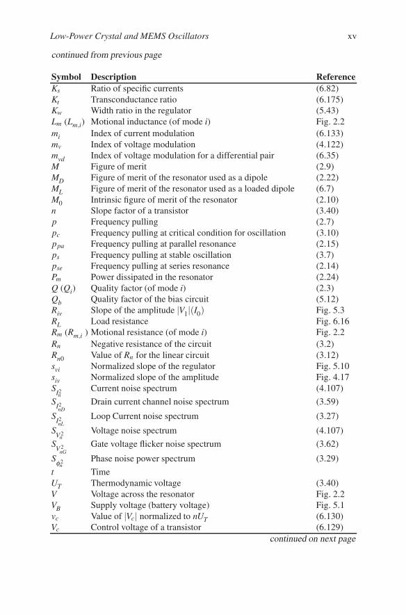
This noise current is added to the oscillation (motional) current Im. For anelementary bandwidth d f at angular frequency ω , the corresponding com-plex phasors are illustrated in Fig. 3.8 at a given instant. Notice that thelength of the noise phasor dIn is a random value of variance SI2
nLd f .
Low-Power Crystal and MEMS Oscillators 33
7
ω ω
∆ω
7
φ
Figure 3.8 Complex phasors of oscillation current Im and elementary noise currentsdInL at a given instant.
Now, since the noise current is small compared to the oscillation current,the power spectrum of the phase noise φn can be expressed as
Sφ 2n
=12
SI2nL
(|Im|/√
2)2=
(1+ γ)kT ω2
Q2Rm|Im|2∆ω2 , (3.29)
where |Im|/√
2 is the RMS value of the oscillation current. The factor 1/2 in-troduced in the first form is due to the fact that only half of the noise power istranslated into phase noise, whereas the other half becomes amplitude noise.
Using expressions (2.24) and (2.23) of the power Pm dissipated in theresonator and of the energy Em of oscillation, (3.29) becomes
Sφ 2n
=(1+ γ)kT ω2
2Q2Pm∆ω2 =(1+ γ)kT ω2QEm∆ω2 . (3.30)
The power spectrum of phase noise is thus proportional to 1/∆ω2. How-ever, this law is no longer valid when ∆ω tends to zero, because of the un-avoidable mechanism of amplitude limitation.
For a given oscillation frequency ω , Sφ 2n
is inversely proportional to theenergy of oscillation Em and to the quality factor Q.
3.7.2 Nonlinear Time Variant Circuit
The results derived in the previous section are only valid if the amplitude ofoscillation is so small that the circuit remains linear and the noise sourcesare time invariant. But to reduce the phase noise, the amplitude must beincreased to increase the motional current Im and the energy of oscillationEm. As a result, the circuit becomes nonlinear and the noise produced by theactive devices becomes cyclostationary (even when it remains white). Phasenoise can then be analyzed by using the impulse sensitivity function (ISF)introduced by Hadjimiri and Lee [6].

34 3 General Theory of High-Q Oscillators
Consider the equivalent circuit of a quartz oscillator at stable oscillationillustrated in Fig. 3.9 It is a second order system with two state variables.
9 9
55 ω
αω
αω
55ω
55ω
Figure 3.9 Equivalent circuit of the oscillator for nonlinear analysis of phase noise.
One is the current flowing through the single inductance Lm. The second isthe total voltage across the capacitances that exchange their energy with theinductance at every cycle of oscillation. The loss resistance Rm and the activedevice that compensates for it are ignored in a first approximation. Indeed,the energy dissipation in Rm during each cycle is 2π/Q the total energy ofoscillation, thus a very small percentage for large values of the quality factorQ. Therefore, we will simplify the analysis by assuming that the voltageacross all the capacitors of the loop is perfectly sinusoidal.
Two separate noise sources are shown, both of them possibly cyclostation-ary. A voltage noise source in series with the inductance and composed of astationary noise Vn(t) multiplied by a modulation function αv synchronouswith the current. A current noise source in parallel with a capacitor Ci Cm
and composed of a stationary noise In(t) multiplied by a modulation functionαi synchronous with the voltage.
According to [6], the phase noise spectrum density resulting from thewhite noise voltage Vn(t) of spectral density SV 2
ncan be expressed as
Sφ 2n
=Γ 2
v ·SV 2n
2(Lm|Im|)2∆ω2 , (3.31)
where Γv is the effective impulse sensitivity function (ISF) given, for the si-nusoidal current |Im|cos φ , by
Γv = −sinφ ·αv(φ). (3.32)
The product Lm|Im| is the maximum magnetic flux in the inductor and ∆ω isgiven by (3.28).

Low-Power Crystal and MEMS Oscillators 35
With a white noise current In(t) source of spectral density SI2n, the phase
noise spectrum is
Sφ 2n
=Γ 2
i ·SI2n
2(Ci|Vi|)2∆ω2 ·(
Cm
Ci
)2
, (3.33)
where Γi is the effective impulse sensitivity function given, for the sinusoidalvoltage |Vi|sinφ , by
Γi = cosφ ·αi(φ). (3.34)
The product Ci|Vi| is the maximum charge in capacitors Ci and Cm. The factor(Cm/Ci) corresponds to the fraction of the total voltage (state variable) thatappears across Ci Cm.
According to [6], the phase noise spectrum density due to a 1/ f flickernoise voltage source of spectral density Kf v/ωn is
Sφ 2n
=Γv
2 ·Kf v
(Lm|Im|)2∆ω3 . (3.35)
The effective ISF Γv is still defined by (3.32), but may be different from thatfor white noise.
With a flicker noise current source of spectral density Kf i/ωn, the phasenoise spectral density is
Sφ 2n
=Γi
2 ·Kf i
(Ci|Vi|)2∆ω3 ·(
Cm
Ci
)2
. (3.36)
The effective ISF Γi is still defined by (3.34), but may be different from thatfor white noise.
The phase noise spectrum density due to white noise sources is propor-tional to 1/∆ω2 and to the mean square value of the corresponding ISF.For 1/ f flicker noise sources, this density is proportional 1/∆ω3 and to thesquare of the mean value of the effective ISF.
The phase noise due to the motional resistance Rm alone can be obtainedby introducing the corresponding thermal noise density SV 2
n= 4kT Rm in
(3.31), with αv = 1 in the expression (3.32) of the effective ISF. ReplacingLm by QRm/ω gives
Sφ 2n
=kT ω2
Q2Rm|Im|2∆ω2 , (3.37)
which is identical to (3.29) for γ = 0 (no contribution of the circuit).

36 3 General Theory of High-Q Oscillators
If the noise current across capacitor Ci comes from the active device thatcompensates for losses, the current delivered by this active device producesa change in voltage Vi. During each period of oscillation, the relative changeof energy in Ci to compensate the loss in Rm must be
∆Ec
Ec=
2πCi
QCm, (3.38)
which is Ci/Cm larger than the relative loss in the resonator itself. Thus, evenwith a large value of Q, the assumption of a sinusoidal voltage Vi acrossC1 becomes a crude approximation when the current is strongly distorted.Without this approximation, the ISF is much more complicated and a precisecalculation of the phase noise can only be obtained by numerical computa-tion.
3.8 Model of the MOS Transistor
The most important nonlinear devices in the circuit are the transistors. Hencetheir proper modelling is essential for nonlinear analyses. Fig. 3.10 shows thesymbols used for N-channel and P-channel MOS transistors. Unlike bipolartransistors, MOS transistors are 4-terminal devices. They have an intrinsicsymmetry that can be preserved in the model by using the local substrate Bas the reference for voltages. This local substrate is normally common to alltransistors of the same type, and is connected to one rail of the power supply(negative rail for the N-channel p-substrate, positive rail for the P-channeln-substate). Hence, the corresponding electrode is usually not represented inschematics, except when it is connected differently.
The static drain current ID of a MOS transistor depends on the valuesof the gate voltage VG, the source voltage VS and the drain voltage VD, all ofthem being defined with respect to the substrate B of the transistor, as definedin Fig. 3.10. According to the EKV model [17,18], it can be expressed as thedifference of two values of a function I(V,VG), for V = VS and V = VD:
ID = I(VS,VG)− I(VD,VG) = IF − IR, (3.39)
where the first term is called the forward (component of) current IF and thesecond the reverse (component of) current IR. A simple but sufficiently accur-ate expression of these symmetrical currents valid in a wide range of currentis [19]

Low-Power Crystal and MEMS Oscillators 37
:
$ ;
;$ ;
:
<
=) (
:
$;
; $;
:
<
= (
Figure 3.10 Definitions of currents and voltages; (a) for a N-channel transistor; (b)for a P-channel transistor.
IF(R) = Ispec
[ln
(1+ exp
VG −VT0 −nVS(D)
2nUT
)]2
, (3.40)
where VT 0 is the threshold voltage (its value for VS = 0), n the slope factor(value ranging from 1.1 to 1.6) and UT = kT/q the thermodynamic voltage(26mV at 27C). Ispec is the specific current of the transistor given by
Ispec 2nµCoxWL
U2T , (3.41)
which depends on the mobility µ of carriers in the channel, on the gate oxidecapacitance per unit area Cox, and on the width-to-length ratio of the channelW/L.
In normal situations (VD > VS for a N-channel transistor), the forward cur-rent IF = I(VS,VG) is larger than the reverse current IR = I(VD,VG).
If IR IF the transistor is in saturation. The drain current becomes inde-pendent on the drain voltage since IF only depends on VG and VS.
If IF(R) Ispec, this component is in weak inversion and can be simplifiedto
IF(R) = Ispec expVG −VT0 −nVS(D)
nUT(3.42)
If IF(R) Ispec, it is in strong inversion and can be simplified to
IF(R) = Ispec
(VG −VT0 −nVS(D)
2nUT
)2
=β2n
(VG −VT0 −nVS(D))2, (3.43)
whereβ µCoxW/L (3.44)
is the transfer parameter that can be used instead of Ispec.The amount of inversion in the transistor can be characterized by the in-
version coefficient IC defined as

38 3 General Theory of High-Q Oscillators
IC max
(IF
Ispec,
IR
Ispec
). (3.45)
If IF and IR are both in weak inversion, the transistor itself operates inweak inversion. Saturation (IR IF ) is then obtained for
VD > VDsat = VS + 4UT to 6UT (saturation in weak inversion). (3.46)
The transistor operates in strong inversion as soon of one of componentsis in strong inversion. Saturation (IR IF ) is then approximately obtainedfor
VD > VDsat =VG −VT0
n= VS +2UT
√IC (satur. in strong inversion). (3.47)
For small variations of the control voltages around a bias point, the deviceremains linear and the variation of drain current can be expressed as
δ ID = −GmsδVS + GmdδVD + GmδVG, (3.48)
where Gm is the usual small-signal gate transconductance, and Gms(d) is thesmall-signal source (drain) transconductance given by
Gms(d) −dIF(R)
dVS(D). (3.49)
It can be obtained by differentiation of (3.40):
Gms(d) =
√IF(R)Ispec
UT
(1− e
−√
IF(R)/Ispec
). (3.50)
For strong inversion, it can be expressed as a function of the voltagesby differentiation of (3.43), or as a function of currents from (3.50) withIF(R) 1:
Gms(d) = β (VG −VT0 −nVS(D)) =
√IF(R)Ispec
UT. (3.51)
In weak inversion, (3.50) becomes simply
Gms(d) = IF(R)/UT (3.52)
It can easily be shown that the more usual gate transconductance is relatedto Gms and Gmd by

Low-Power Crystal and MEMS Oscillators 39
Gm dID
dVG=
Gms −Gmd
n. (3.53)
Hence in weak inversion:
Gm =1n
[IF
UT− IR
UT
]=
ID
nUT(weak inversion). (3.54)
In forward saturation, IR IF and Gmd Gms. The general expressionof the gate transconductance is then:
Gm =Gms
n=
√IDIspec
nUT
(1− e−
√ID/Ispec
)=
ID
nUT· 1− e−
√IC
√IC
, (3.55)
In strong inversion, it is reduced to
Gm =Gms
n=
√IDIspec
nUT=
ID
nUT
√IC
=
√2β ID
n=
βn
(VG −VT0 −nVS).
(3.56)It should be mentioned that even in saturation (i.e. for ID = IF ), the drain
current ID remains slightly dependent on the drain voltage, due to the phe-nomenon of channel length modulation. This effect can be modelled by asource-to-drain conductance Gds that can be approximated by
Gds = ID/VM , (3.57)
where VM is the channel length modulation voltage, proportional to the lengthL of the channel. If the channel is not too short (sufficiently longer than theminimum length allowed by the process), the intrinsic voltage gain of thetransistor in saturation
AV0 Gm/Gds =VM
nUT· 1− e−
√IC
√IC
(3.58)
is much larger than unity but is reduced for large values of IC.The most fundamental source of noise of the transistor is its channel noise.
It can be modelled by a noise current of spectral density SI2nD
independent of
the frequency, which is added to the drain current. For VD = VS (thus forID = IF − IR = 0), this noise is the thermal noise of the channel conductanceequal to Gms and Gmd :
SI2nD
= 4kT Gms for VD = VS (3.59)

40 3 General Theory of High-Q Oscillators
As shown by Fig. 3.11, when the transistor is saturated this spectral densityis reduced to
SI2nD
= 4kT γtGms = 4kT γtnGm in saturation, (3.60)
where γt is the channel noise excess factor of the transistor, of value 1/2 inweak inversion and 2/3 in strong inversion. These values can be higher inshort-channel devices. Notice that in saturation, the noise of the transistor
;$%;$
%
, >
;$#!;;
!
*
&
!
;
%
;$% >
#!;;!
?3
!
;
Figure 3.11 Variation of the channel noise spectral density with increasing VDS =VD −VS.
in weak inversion is the shot noise associated with the forward current IF =ID IR:
SI2nD
= 2qID (saturated weak inversion). (3.61)
In strong inversion, the noise for a given value of drain current is reduced,since Gms/ID is reduced.
Flicker noise due to carrier trapping and mobility fluctuations is also im-portant in MOS transistors. Since its spectral density is inversely propor-tional to the frequency, it dominates at low frequencies. It can be approxim-ated by a noise voltage VnG added to the gate voltage, with a spectral densitySV 2
nGgiven by
SV 2nG
=Kf
ωnwhere Kf ∝
1W L
. (3.62)
This noise voltage is minimum in moderate inversion and increases onlyslowly in weak and in strong inversion. Hence, in a first approximation, Kfcan be considered constant. In a given process, it can be reduced by increas-ing the gate area WL.

Chapter 4Theory of the Pierce Oscillator
4.1 Basic Circuit
The simplest possible oscillator uses a single active device to generate the re-quired negative resistance. If no inductance is available, the only possibilityis the 3-point oscillator developed in 1923 by G. W. Pierce [2, 3]. The prin-ciple of this oscillator is depicted in Fig. 4.1. The active device is assumed to
;
:
Figure 4.1 Basic 3-point Pierce oscillator (biasing omitted).
be a MOS transistor, but it could be a bipolar transistor as well. The sourceof the MOS transistor is connected to its substrate, to make it a 3-terminaldevice. The bias circuitry needed to activate the transistor is omitted here.Capacitors C1 and C2 connected between gate and source, respectively drainand source, are functional: they must have finite values in order to obtain anegative resistance across the motional impedance of the resonator.
This oscillator is very similar to the Clapp circuit [20], except for thepresence of the unavoidable capacitance in parallel with the series motional
E. Vittoz, Low-Power Crystal and MEMS Oscillators: The Experience of Watch Developments, 41Integrated Circuits and Systems, DOI 10.1007/978-90-481-9395-0_4, © Springer Science+Business Media B.V. 2010

42 4 Theory of the Pierce Oscillator
resonator. The presence of this capacitance has important implications on thebehavior of the circuit.
Assuming that the transistor is saturated, the equivalent circuit of thisstructure is that of Fig. 4.2.
;
;
;
#
;:
":
Figure 4.2 General equivalent circuit of the Pierce oscillator.
The active part of the saturated transistor is represented by the voltage-controlled current source ID(VG). The three passive dipoles D1, D2 and D3include all remaining parts of the equivalent circuit of the transistor itself,as well as the functional and parasitic components of the biasing circuitry.Moreover, in accordance with Fig. 3.1(a), D3 includes the capacitance C12of the quartz resonator, whereas C10 and C20 are included in D1 and D2 re-spectively. Notice that each of these three dipole may be nonlinear, as forexample D1 if the active device is a bipolar transistor. The rest of the circuitis the motional impedance Zm of the resonator.
4.2 Linear Analysis
4.2.1 Linearized Circuit
Linearizing the general equivalent circuit of Fig. 4.2 around a biasing pointof the active device results in the equivalent circuit of impedance Zc depictedin Fig. 4.3(a). Assuming no inductance dominates, the three passive dipolesDi becomes linear complex impedance given by
Zi =1
Gi + jωCi, (4.1)

Low-Power Crystal and MEMS Oscillators 43
#
#
Figure 4.3 Linearized equivalent circuit of the oscillator.
that are practically independent of slight amount of frequency pulling p 1.The voltage-controlled current source becomes GmV1, where Gm is the gatetransconductance of the transistor and V1 the complex voltage across Z1.
The linear circuit impedance Zc can easily be expressed as
Zc =Z1Z3 + Z2Z3 + GmZ1Z2Z3
Z1 + Z2 + Z3 + GmZ1Z2, (4.2)
which corresponds to the compact small-signal model of Fig. 4.3(b). Thecircuit impedance Zc is thus a bilinear function of Gm. Bilinear functionstransform circles into circles in the complex plane [8], therefore the locusof Zc(Gm) for Gm changing from −∞ to +∞ (circle of infinite radius) is acircle, as illustrated in Fig. 4.4. It should not be confused with the locus ofZc(1)(|Ic|) represented in Fig. 3.3.
Since the reactive components of Zi are all capacitive, this circle is locatedin the lower half of the complex plane (negative imaginary part). The realpart of Zc can only be negative (providing a negative resistance) when thecircuit is made active by a positive value of Gm. However, the circuit remainspassive if Gm is too small to compensate the losses due to the reals part of Zi.Moreover, as can be seen in the figure, is also remains passive if Gm is toolarge.
The real value of Zc is minimum for a particular value Gmopt of transcon-ductance. It is the maximum absolute value of negative resistance |Rn0|max
that can be obtained.The locus of −Zm(p) given by (2.8) is plotted in dotted line in the same
figure. It is a vertical strait line at distance −Rm of the imaginary axis.According to (3.8), the critical condition for oscillation is reached at the
intersection of the two loci. For the particular case depicted in Fig. 4.4, thereare two solutions labelled A and B. We will show later that solution B isunstable, because it does not fulfill the condition (1.2) for phase stability.

44 4 Theory of the Pierce Oscillator
#
#
@ A
55"
4
<
=#
=#"
ω
!
Figure 4.4 Loci of Zc(Gm) and −Zm(p) in the complex plane.
The only stable solution is at intersection A, for the particular value Gmcrit ofGm called critical transconductance for oscillation.
If Gm is increased beyond Gmcrit , the oscillation will start up and growexponentially with time constant τ0 given by (3.15) (as long as the circuitremains linear). A maximum amount of net negative resistance Rn0 + Rm isobtained for Gm = Gmopt , corresponding to a minimum value of time con-stant τ0. If Gm is increased beyond Gmcrit , τ0 starts increasing again, until itbecomes infinite at point B, for Gm = Gmmax.
If the quality factor Q given by (2.3) decreases, then Rm increases and theintersection points A and B move to the left. They approach each other, untilthey merge into a single point, when −Zm(p) becomes tangent to Zc(Gm). Nosolution exists for Rm > |Rn0|max; no oscillation is then possible, whatever thevalue of transconductance Gm.
For the critical condition, the frequency pulling p takes the value pc ob-tained by equating the imaginary part of Zc at point A with that of −Zm givenby (2.8). This yields
pc = −ωCm
2Im(Zc|A). (4.3)
Now, it is important to notice that the variation of Rm due to a variation ofquality factor Q moves the point A not only horizontally, but also vertically,proportionally to the slope dIm(Zc)/dRe(Zc) at point A. Hence, accordingto (4.3):

Low-Power Crystal and MEMS Oscillators 45
dpc
dQ/Q= − dpc
dRm/Rm= −ωCmRm
2dIm(Zc)dRe(Zc)
|A = − 12Q
dIm(Zc)dRe(Zc)
|A. (4.4)
Since, even in good resonators, the quality factor can change by a largeamount with temperature variations, this sensitivity to the quality factorshould be minimized to avoid a degradation of the frequency stability. Thiscan be obtained by pushing the point A as close as possible to the top ofthe circle, where the sensitivity is zero (horizontal tangent). Notice that thissensitivity tends to infinity when Rm approaches |Rn0|max.
The radius of the circle increases with the value of Z3. If Z3 is infinite,then
Zc = Z1 + Z2 + GmZ1Z2 for Z3 = ∞ (4.5)
becomes a linear function of Gm. As illustrated in Fig. 4.5, this correspondsto a circle of infinite radius. The maximum value of |Rn0| is no longer limited,
#@
@
!
δ
δ
δδ
Figure 4.5 Locus of Zc(Gm) for infinite Z3.
and the slope of this strait-line locus would be zero if Z1 and Z2 would bepurely capacitive. However, if the capacitors have losses represented by theirloss angles δ1 and δ2 as shown in the figure, the locus of Zc(Gm) has a slopecharacterized by an angle δ1 + δ2, and some sensitivity of pc to Q remains.
Notice that an infinite value of Z3 cannot be obtained with an electromech-anical resonator. Indeed, since the figure of merit M0 defined by (2.10) isnever infinite, the electrical capacitance C12 always remains as a componentof Z3. The situation of Fig. 4.5 can be approached by using large values ofC1 and C2, in order to obtain Z1 + Z2 Z3 for Gm Gmopt .

46 4 Theory of the Pierce Oscillator
4.2.2 Lossless Circuit
To obtain a maximum activity and a minimum sensitivity of the frequency tothe quality factor, the circuit should be made of lossless capacitors, thus
Zi =1
jωCi(4.6)
The expression (4.2) of the circuit impedance then becomes
Zc =−GmC1C2 − j[ω(C1 +C2)(C1C2 +C2C3 +C3C1)+ G2
mC3/ω ]ω2(C1C2 +C2C3 +C3C1)2 +(GmC3)2 . (4.7)
The locus Zc(Gm) of Fig. 4.4 is now centered on the imaginary axis, as shownin Fig. 4.6. The right half of the circle corresponding to negative values oftransconductance is of no practical interest. For Gm = 0 the circuit impedance
#
#
@
A
ω%
4
<
"
#ω%
!
ω
ω
55"
Figure 4.6 Loci of Zc(Gm) and −Zm(p) in the complex plane for a lossless circuit.
is imaginary and has the value
Zc =− j
ω(C3 +Cs)for Gm = 0, (4.8)
where Cs is the series combination of C1 and C2:
Cs =C1C2
C1 +C2(4.9)

Low-Power Crystal and MEMS Oscillators 47
It is also imaginary for Gm = ∞ where it has the value
Zc =− j
ωC3for Gm = ∞. (4.10)
Some negative resistance is produced for 0 < Gm < ∞, with a maximumgiven by the radius of the circle. Hence, from (4.8) and (4.10):
|Rn0|max =1
2ωC3(1+C3/Cs). (4.11)
The minimum possible value of the start-up time constant τ0 can be ob-tained by introducing this expression in (3.15):
1τ0min
= ω(
Cm
4C3(1+C3/Cs)− 1
2Q
)=
ω2Q
(M
2(1+C3/Cs)−1
), (4.12)
where the figure of merit M is defined by (2.9).The value of transconductance producing this maximum can be obtained
by equating to zero the first derivative of the real part of Zc in (4.7). Thisgives
Gmopt = ω(
C1 +C2 +C1C2
C3
). (4.13)
By using the fact that the locus of Zc(Gm) is a centered circle of radius|Rn0|max, and remembering that Re(Zc) = Rn0, the imaginary part of the cir-cuit impedance can be expressed as
Im(Zc) = − 1ω(Cs +C3)
−|Rn0|max
⎡⎣1±
√1−
( |Rn0||Rn0|max
)2⎤⎦ , (4.14)
whereas the slope of the locus is given by
dIm(Zc)dRe(Zc)
=±1√(
|Rn0|max
|Rn0|
)2−1
. (4.15)
It is zero on the imaginary axis (|Rn0| = 0) and infinite for |Rn0| = |Rn0|max.The locus of −Zm(p) is also reported in Fig. 4.6, for a particular value of
motional resistance Rm. A necessary condition for oscillation is that Rm =|Rn0|< |Rn0|max. By introducing (4.11), (2.3) and (2.9), this condition can beexpressed as
M =QCm
C3> 2(1+C3/Cs) > 2. (4.16)

48 4 Theory of the Pierce Oscillator
Hence no oscillation is possible with the Pierce oscillator if the factor ofmerit M of the resonator (and a fortiori its intrinsic value M0) is smaller thantwo. This is because the lumped impedance between the drain and the gatein Fig. 4.1 must become inductive.
Moreover, the condition (4.16) must be fulfilled with a large margin, inorder to limit the sensitivity the oscillator frequency to variations of Q. Thuswe shall impose a margin factor
Km |Rn0|max
Rm=
M2(1+C3/Cs)
1. (4.17)
Then, according to (4.4) and (4.15) the sensitivity at of the frequency at thestable solution A is given
dpc
dQ/Q=
−1
2Q√
K2m −1
. (4.18)
It is drastically degraded when Km approaches 1.The exact amount of frequency pulling at the stable point A is obtained
by introducing (4.14) (with the minus sign in the parenthesis) and (4.17) into(4.3), giving
pc =Cm
2(Cs +C3)+
Cm
4C3(1+C3/Cs)
(1−
√1− 1
K2m
). (4.19)
If K2m 1, this expression can be approximated by
pc∼=
Cm
2(Cs +C3)+
12QM
(1+
C3
Cs
). (4.20)
Now, since usually QM (Cs +C3)/Cm, this result can be further simpli-fied by neglecting the second term:
pc∼= Cm
2(Cs +C3). (4.21)
The amount of frequency pulling is then independent of the quality factor.The capacitance that is responsible for the frequency pulling, in this caseCs +C3, is usually called (in quartz data sheets) the load capacitance of theresonator.
The value of transconductance at solutions A and B in Fig. 4.6 is obtainedby equating the real part of Zc in (4.7) with −Rm and solving for Gm. Thisyields

Low-Power Crystal and MEMS Oscillators 49
Gm =C1C2
2RmC23
⎡⎣1±
√1−
[2M
(1+
C3
Cs
)]2⎤⎦ , (4.22)
where the positive sign gives the maximum value (at point B) and the negat-ive sign gives the critical value. According to (4.17) the squared term in thesquare root is 1/K2
m. If K2m 1, this result can be approximated to give the
maximum transconductance
Gmmax∼=
C1C2
RmC23
=ωCmC1C2Q
C23
= MωC1C2
C3, (4.23)
and the critical transconductance (for the lossless circuit)
Gmcrit0∼= ω2RmC1C2(1+C3/Cs)2 =
ωQCm
C1C2(1+C3/Cs)2. (4.24)
It is worth noticing that the ratio
Gmmax
Gmcrit0
∼=M2
(1+C3/Cs)2∼=︸︷︷︸
for C3Cs
M2 (4.25)
is essentially dependent on the figure of merit M.It is interesting to replace the squared parenthesis in (4.24) by its value
obtained from (4.21). The critical transconductance can then be expressed as
Gmcrit0∼=
ωCm
Qp2c
(C1 +C2)2
4C1C2=︸︷︷︸
for C2=C1
ωCm
Qp2c. (4.26)
For a given quartz resonator, the critical transconductance is thus inverselyproportional to the square of the frequency pulling pc and is minimum forC1 = C2. Hence, decreasing the sensitivity of the frequency of oscillation tocircuit parameters by decreasing pc requires a large increase of bias current.This is especially true if the device is a MOS transistor operated in strong in-version: indeed, the transconductance is then only proportional to the squareroot of the bias current; decreasing pc by a factor 10 would then require10’000 more current!
For C1 = C2 (4.24) becomes
Gmcrit0∼= ω2Rm(C1 + 2C3)
2 =ω
QCm(C1 + 2C3)
2. (4.27)

50 4 Theory of the Pierce Oscillator
4.2.3 Phase Stability
In order to verify the phase stability condition (1.2), the overall oscillator canbe opened at the gate of the transistor, as illustrated in Fig. 4.7.
6
Figure 4.7 Open-loop oscillator for calculation of gain G.
The open-loop gain G is then easily calculated to be
G =V
′1
V1=
−GmZ1Z2
Z1 + Z2 + Z3Zm
Z3+Zm
, (4.28)
where Zm is given by (2.8) and Z1 to Z3 by (4.6) for a lossless oscillator. Tosimplify the analysis, let us assume that |Z1 + Z2| |Z3Zm(Z3 + Zm)| (verylarge values of C1 and C2), which should have no effect on the phase stability.The tangent of the argument of G is then obtained as
tan (argG) =4C3
ωC2mRm
p2 − 2pωCmRm
+ ωC3Rm, (4.29)
the derivative of which is
d(tan (arg G))dp
=2
ωC3Rm
(4pC3
Cm−1
). (4.30)
Now, since the sign of d(arg G)/dω is the same as that of d(tan (arg G))/dp,condition (1.2) becomes
stable phase for p <Cm
4C3(point A) (4.31)
unstable phase for p >Cm
4C3(point B). (4.32)
Thus, point A of figures 4.4 and 4.6 is indeed stable, whereas point B inunstable.

Low-Power Crystal and MEMS Oscillators 51
4.2.4 Relative Oscillator Voltages
By lumping the parallel impedances Zm and Z3 in to a single impedance Zx,the overall oscillator at small signals can be redrawn as shown in Fig. 4.8.
$"
#
Figure 4.8 Calculation of voltage ratios.
Now, since Z3 is already included in Zx, at the critical condition (3.8) foroscillation, according to (4.5)
Zx = −Zc|Z3=∞ = −(Z1 + Z2 + GmcritZ1Z2). (4.33)
Voltage ratios can then easily be calculated by means of Fig. 4.8:
V2
V1= 1+
Zx
Z1= −Z2
(1Z1
+ Gmcrit
), (4.34)
with a modulus
|V2||V1|
=
√(G1 + Gmcrit)2 +(ωC1)2
G22 +(ωC2)2 , (4.35)
andV3
V1=
Zx
Z1=
V2
V1−1. (4.36)
with a modulus
|V3||V1|
=
√(G1 + G2 + Gmcrit)2 + ω2(C1 +C2)2
G22 +(ωC2)2 . (4.37)
For a lossless circuit with a large margin factor Km, the critical transcon-ductance is given by (4.24), and the voltage ratio becomes
V2
V1= −C1
C2+ j
C1
QCm
(1+
C3
C1+
C3
C2
)2
. (4.38)
If C2 is not too large, the imaginary part of this expression is usually smalleror much smaller than C1/C2. Then, for C1 = C2, V2
∼= −V1 and V3∼= −2V1.

52 4 Theory of the Pierce Oscillator
4.2.5 Effect of Losses
4.2.5.1 Numerical Example
The effect of losses on the locus of Zc(Gm) is obtained by introducing the fullexpression of Z1, Z2 and Z3 given by (4.1) in the equation (4.2) of Zc, whichgives a very complicated analytical result. A numerical example is shown inFig. 4.9 with particular values corresponding to a realistic case of a 32 kHzoscillator with large losses.
Figure 4.9 Example of the effect of loss conductance G1, G2 and G3 on the locusof Zc(Gm).
As can be seen, the circle is moved to the right of the complex plane,thereby reducing the amount of negative resistance. The corresponding ef-fects on the critical transconductance can be obtained by equating the realpart of −Zc(Gm) to the motional resistance Rm = 1/(ωCmQ), thereby provid-ing Q(Gm). The result obtained with the same numerical values is shown inFig. 4.10(a).
Losses result in an increase of the critical transconductance
Gmcrit = Gmcrit0 + ∆Gmcrit (4.39)
Ω
Ω
μμμ

Low-Power Crystal and MEMS Oscillators 53
Figure 4.10 Example of the effect of loss conductance G1, G2 and G3; (a) on thecritical transconductance; (b) on the amount of frequency pulling.
where ∆Gmcrit is approximately independent of the quality factor. In thisexample, Gmcrit is increased by a factor 6 for Q = 105.
The effect of losses on the frequency pulling pc calculated by (4.3) isshown in Fig. 4.10(b) for the same numerical values. It is smaller than 10−5
for Q = 105. This figure also shows the dependency of pc on Q that wasdiscussed in Section 4.2.1.
4.2.5.2 Approximative Expression for the Increase of Gm
An inspection of Fig. 4.9 shows that if the shift of the circle is small withrespect to its radius, then the effect of losses is approximately equivalent toan increase ∆Rm of the motional resistance given by
∆Rm = Re(Zc)|Gm=0. (4.40)
Then, according to (4.24)
∆Gmcrit∼= ω2C1C2(1+C3/Cs)2∆Rm. (4.41)
For Gm = 0, the expression (4.2) of Zc is reduced to
|Zc|Gm=0 =1
1/(Z1 + Z2)+ 1/Z3. (4.42)
µµµµ

54 4 Theory of the Pierce Oscillator
If the losses are small with
G2i (ωCi)
2, (4.43)
then
Re(Zc)|Gm=0 =G1C
22 + G2C
21 + G3(C1 +C2)
2
ω2(C1C2 +C2C3 +C3C1)2 (4.44)
By introducing (4.40) and (4.44) in (4.41), the increase of critical transcon-ductance due to losses can be approximated by
∆Gmcrit∼=
G1C22 + G2C
21 + G3(C1 +C2)
2
C1C2. (4.45)
Notice that this approximation is independent of C3. For C1 = C2, it becomes
∆Gmcrit∼= G1 + G2 + 4G3, (4.46)
showing the larger effect of the drain-gate conductance G3.
4.2.6 Frequency Adjustment
The mechanical resonant frequency ωm of the resonator cannot be adjustedwith a precision better than about 10 ppm. It is therefore usually necessaryto fine tune the frequency of oscillation by electrically adjusting the amountof frequency pulling p, given in a good approximation by (4.21).
One possibility would be to adjust capacitor C3. However, this is not agood solution, since C3 should remain as small as possible to maximize theradius of the circular locus of Zc(Gm).
Best would be to adjust C1 and C2 while maintaining C1 = C2, since itensures a minimum of critical transconductance for a given amount of fre-quency pulling, as expressed by (4.26). It is usually more convenient to adjustonly one capacitor.
Now the relative range of frequency adjustement can be expressed as
ωmax −ωmin
ω= pmax − pmin. (4.47)
To increase pmax, C1 and/or C2 must be reduced. This increases the relativeimportance of parasitic capacitors (usually voltage-dependent) and reducesthe radius of the circular locus of Zc(Gm). The frequency stability is thereforedegraded. The absolute maximum of p for stable oscillation is reached at the

Low-Power Crystal and MEMS Oscillators 55
point corresponding to Gmopt in Fig. 4.4. Calculation for a lossless circuit(Fig. 4.6) yields
pmaxmax =Cm
2C3
(1− 1
M
), (4.48)
which is lower than the pulling ppa at parallel resonance given by (2.15).According to (4.26), a reduction of pmin increases the critical transcon-
ductance and therefore the power consumption of the oscillator. The abso-lute minimum of p would be reached for infinite values of C1 and C2 (henceinfinite critical transconductance) and is equal to its value at series resonancegiven by (2.14).
The maximum possible range of frequency adjustment is thus limited byconsiderations on frequency stability and power consumption. In practice, itis never more than a small fraction of Cm/(2C3).
In some applications like time-keeping, the precise adjustment of the os-cillator can be replaced by adjusting the ratio of the following frequencydivision chain. The amount of pulling can then be kept at an optimal valuewith respect to power consumption and frequency stability.
4.3 Nonlinear Analysis
4.3.1 Numerical Example
As soon as the critical transconductance is exceeded, the amplitude of os-cillation increases until it is limited by nonlinear effects. As explained inSection 3.1, these nonlinear effects can be analyzed by computing the circuitimpedance for the fundamental frequency Zc(1) defined by (3.1).
As an example, consider the simple Pierce oscillator circuit shown inFig. 4.11(a). The active N-channel transistor is biased by means of the cur-rent I0 (mirrored by the P-channel transistors) and the resistor R connectedbetween drain and gate. The locus of Zc(1)(Ic) has been calculated accordingto the procedure introduced in Section 3.1, by using the EKV model [18] ofMOS transistors for a standard a 0.18 µm process. The extraction of the fun-damental component V(1) of the voltage resulting from the sinusoidal currentIc forced into the circuit was obtained by simulating an LC filter tuned atexactly the same frequency.
The results at a frequency of 32kHz are depicted in Fig. 4.11(b) for severalvalues of bias current I0.

56 4 Theory of the Pierce Oscillator
5 5C8%4E
&
&
&
&'
&-
&
+&'
&'
,&'
&'
Cµ4E #'4
#&-4
%#3F
#3Ω
&',&' !
#+4
#+&-4
5 5#
#&+4
#/
#/ #/
#D
Ω
&#µ#µ
&#µ#µ
<#&'8
;9
Figure 4.11 Example of nonlinear effects in a Pierce oscillator: (a) Circuit schem-atic with numerical values; (b) Loci of Zc(1)(Ic) for several values of bias I0 at32kHz.
The circle in dotted line is the theoretical locus of Zc(Gm) for the linearcircuit. It includes the losses due to bias resistor R, but not those due to theoutput conductance of the transistors.
For a bias current I0 = 0.6 µA, these additional losses are negligible andthe locus of Zc(1)(Ic) starts on the circle. It remains on the circle (Zc(1) =Zc) as long as the amplitude |Ic| ≤ 10nA. Indeed, assuming that all the ACcurrent flows through C1, 10nA flowing in 20pF produce a voltage of about5mV, for which the circuit remains linear. For |Ic| = 100nA, the circuit isalready nonlinear: the locus leaves the circle and the negative resistance isreduced. It is further reduced when the amplitude increases. For 10µA andabove, the losses are so high that the real part of Zc(1)) becomes positive (nonegative resistance produced by the circuit).
For a bias current I0 = 1 µA, more negative resistance is produced (closeto the maximum possible), but the losses due to the output conductance ofthe active transistor are no longer negligible: the locus of Zc(1)(Ic) does notstart exactly on the circle.
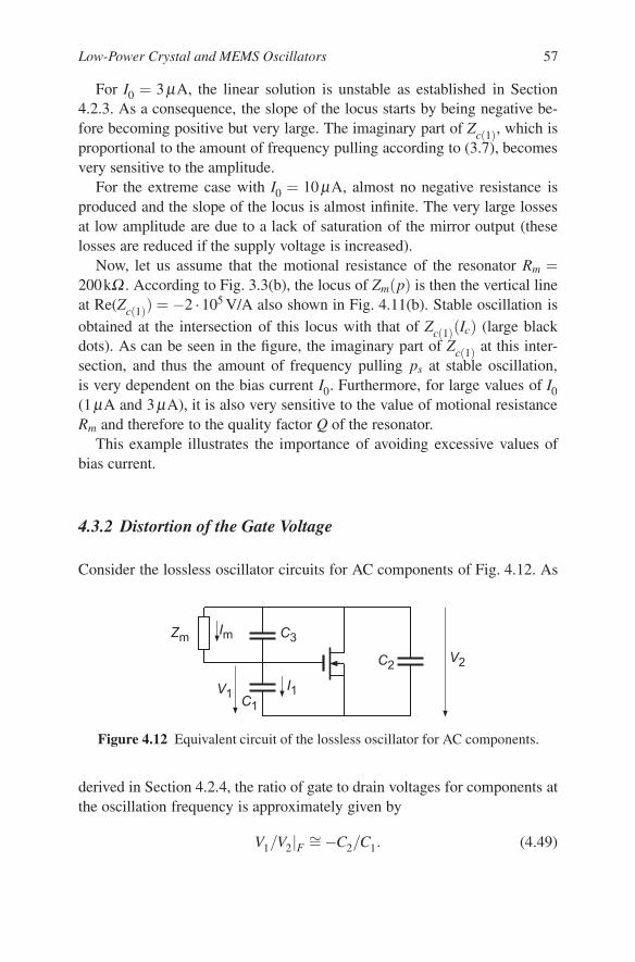
Low-Power Crystal and MEMS Oscillators 57
For I0 = 3 µA, the linear solution is unstable as established in Section4.2.3. As a consequence, the slope of the locus starts by being negative be-fore becoming positive but very large. The imaginary part of Zc(1), which isproportional to the amount of frequency pulling according to (3.7), becomesvery sensitive to the amplitude.
For the extreme case with I0 = 10 µA, almost no negative resistance isproduced and the slope of the locus is almost infinite. The very large lossesat low amplitude are due to a lack of saturation of the mirror output (theselosses are reduced if the supply voltage is increased).
Now, let us assume that the motional resistance of the resonator Rm =200kΩ . According to Fig. 3.3(b), the locus of Zm(p) is then the vertical lineat Re(Zc(1)) = −2 · 105 V/A also shown in Fig. 4.11(b). Stable oscillation isobtained at the intersection of this locus with that of Zc(1)(Ic) (large blackdots). As can be seen in the figure, the imaginary part of Zc(1) at this inter-section, and thus the amount of frequency pulling ps at stable oscillation,is very dependent on the bias current I0. Furthermore, for large values of I0(1 µA and 3 µA), it is also very sensitive to the value of motional resistanceRm and therefore to the quality factor Q of the resonator.
This example illustrates the importance of avoiding excessive values ofbias current.
4.3.2 Distortion of the Gate Voltage
Consider the lossless oscillator circuits for AC components of Fig. 4.12. As
Figure 4.12 Equivalent circuit of the lossless oscillator for AC components.
derived in Section 4.2.4, the ratio of gate to drain voltages for components atthe oscillation frequency is approximately given by
V1/V2|F ∼= −C2/C1. (4.49)

58 4 Theory of the Pierce Oscillator
But for harmonic components of the drain voltage, the motional impedanceZm is almost infinite, therefore the drain to gate voltage ratio is simply givenby the capacitive divider C1 −C3:
V1/V2|H =C3
C1 +C3. (4.50)
The relative attenuation of harmonics is thus
V1/V2|HV1/V2|F
∼=C3C1
(C1 +C3)C2. (4.51)
Therefore, even if the drain voltage is strongly distorted, the gate voltagecan remain sinusoidal if C3 = 0 (or more generally if Z3 = ∞). Practically, itremains almost sinusoidal if C3 C2.
It must be pointed-out that it is very important to limit the amount of dis-tortion of the gate voltage. Indeed, harmonic components can be intermod-ulated by the nonlinear transfer function of the transistor, thereby producingan additional fundamental component of drain current. Since the phase ofthis additional component will be different from that of the main compon-ent, the frequency of oscillation will be shifted by nonlinear effects.
For Z3 = ∞, the gate signal would remain perfectly sinusoidal, hence thenonlinear transfer function would have no effect on the frequency. Referringto Fig. 3.3(b), this means that the locus of Zc(1)(|Ic|) would be an horizontalstraight line.
4.3.3 Amplitude Limitation by the Transistor Transfer Function
4.3.3.1 Introduction
When the oscillation grows up, it is usually first limited by the nonlineartransfer function of the active device, as illustrated in Fig. 4.13. Part (a) ofthe figure shows the oscillator circuit with its bias current I0. A resistivepath Rb is provided between drain and gate so that, at equilibrium, the DCcomponent of the drain current ID can reach the imposed value I0. The supplyvoltage VB must be large enough in order to maintain I0 constant even duringthe positive peaks of drain voltage.
As was discussed in Section 4.3.2, the gate voltage of amplitude |V1| re-mains approximately sinusoidal, with
VG(t) = VG0 + |V1|sin ωt, (4.52)

Low-Power Crystal and MEMS Oscillators 59
;'
<
φ#ω
;
55
:φ#ω
;
5(5
Figure 4.13 Amplitude limitation by the nonlinear transfer function of a transistor;(a) basic circuit; (b) mechanism of limitation.
But when its amplitude grows, the drain current ID is distorted by the non-linearity of ID(VG), as shown in part (b) of the figure, and
ID(t) = I0 + |ID(1)|sinωt + harmonic components. (4.53)
The harmonic components cannot flow through the motional impedance,and therefore flow mainly through capacitor C2. The only useful componentof ID is the fundamental component of amplitude |ID(1)|. Hence the relevanttransconductance is that for the fundamental frequency, defined by
Gm(1) |ID(1)||V1|
=ID(1)
V1. (4.54)
It is a real value as long as no phase shift exists in the transistor itself.Now, because of the creation of harmonics, |ID(1)| grows less than linearly
with |V1| and therefore Gm(1) decreases when |V1| increases. The latter stopsincreasing when the condition for stable oscillation is reached for
Gm(1) = Gmcrit , (4.55)
where Gmcrit is given by (4.39), (4.24) and (4.45). The amplitude obtained fora given current depends on the critical transconductance and on the width-to-length ratio of the transistor, which affects the specific current Ispec definedby (3.41).

60 4 Theory of the Pierce Oscillator
4.3.3.2 Transistor in Weak Inversion
Let us assume that the transistor remains in weak inversion even for the peakvalue of drain current. In order to avoid losses, it should also remain saturated(fulfilling condition (3.46)), even for the minimum value of drain voltage.Thus ID = IF and weak inversion is ensured if Ispec IDmax. Since the sourcevoltage VS = 0, the drain current given by the model described in Section 3.8is
ID
Ispec= exp
VG −VT0
nUT= exp
VG0 −VT0 + |V1|sin φnUT
= eve+v1 sinφ , (4.56)
where φ = ωt and
ve =VG0 −VT0
nUTand v1 =
|V1|nUT
(4.57)
are normalized variables.Notice that saturation may be difficult to ensure with a large drain voltage
amplitude if VT0 is too small. This problem will be discussed in Section 5.1.6.The DC component of drain current is obtained by averaging (4.56) over
one period:
I0
Ispec= eve · 1
2π
∫ 2π
0ev1 sinφ dφ = eve · IB0(v1), (4.58)
where
IB0(v1) = 1+v2
1
22 +v4
1
22 ·42 +v6
1
22 ·42 ·62 + · · · (4.59)
is the modified Bessel function of order 0.The fundamental component of drain current is given by
|ID(1)|Ispec
= eve · 1π
∫ 2π
0ev1 sinφ sinφ dφ = eve ·2IB1(v1), (4.60)
where
IB1(v1) =v1
2+
v31
22 ·4 +v5
1
22 ·42 ·6 +v7
1
22 ·42 ·62 ·8 + · · · (4.61)
is the modified Bessel function of order 1.The transconductance for the fundamental frequency can then be ex-
pressed as a function of the bias current I0 and of the normalized gate voltageamplitude v1 by introducing (4.57), (4.58) and (4.60) into (4.54), which gives
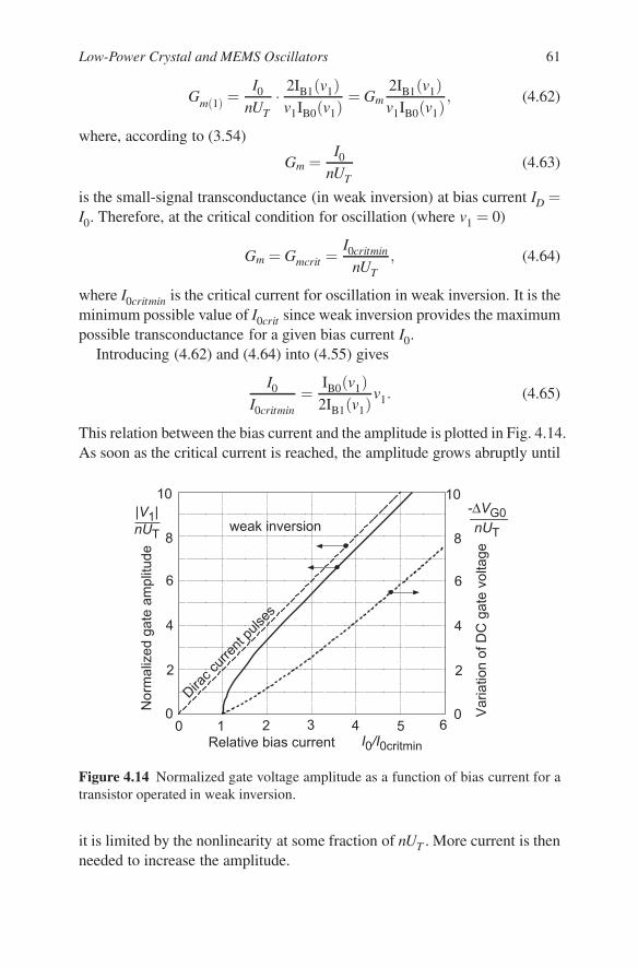
Low-Power Crystal and MEMS Oscillators 61
Gm(1) =I0
nUT· 2IB1(v1)
v1IB0(v1)= Gm
2IB1(v1)v1IB0(v1)
, (4.62)
where, according to (3.54)
Gm =I0
nUT(4.63)
is the small-signal transconductance (in weak inversion) at bias current ID =I0. Therefore, at the critical condition for oscillation (where v1 = 0)
Gm = Gmcrit =I0critmin
nUT, (4.64)
where I0critmin is the critical current for oscillation in weak inversion. It is theminimum possible value of I0crit since weak inversion provides the maximumpossible transconductance for a given bias current I0.
Introducing (4.62) and (4.64) into (4.55) gives
I0
I0critmin=
IB0(v1)2IB1(v1)
v1. (4.65)
This relation between the bias current and the amplitude is plotted in Fig. 4.14.As soon as the critical current is reached, the amplitude grows abruptly until
Figure 4.14 Normalized gate voltage amplitude as a function of bias current for atransistor operated in weak inversion.
it is limited by the nonlinearity at some fraction of nUT . More current is thenneeded to increase the amplitude.
Δ

62 4 Theory of the Pierce Oscillator
As the amplitude increases, the duration of the peaks of drain current isprogressively reduced. If these peaks of current would be Dirac functions(zero duration and infinite amplitude), then |ID(1)|/I0 = 2. Introducing (4.62)and (4.64) into (4.55) would then give
v1 =|V1|nUT
= 2I0
I0critmin. (4.66)
This asymptotic linear behavior is also represented in Fig. 4.14. It is a reas-onable approximation of weak inversion for |V1| nUT .
What is the variation of ve (and thus of the DC gate voltage VG0) when theamplitude increases? For stable oscillation, (4.55) and (4.60) give
Gmcrit = Gm(1) =|ID(1)||V1|
=|ID(1)|v1nUT
=Ispec
nUT· eve ·2IB1(v1)
v1. (4.67)
Solving for ve results in
ve =VG0 −VT 0
nUT= ln
I0critmin
Ispec− ln
2IB1(v1)v1︸ ︷︷ ︸
∆VG0/(nUT )
. (4.68)
The normalized value of DC gate voltage variation ∆VG0 is also represented(in dotted line) in Fig. 4.14.
4.3.3.3 Larger Amplitude by Capacitive Attenuator
As shown by Fig. 4.14, to obtain a gate voltage amplitude larger than a fewnUT in weak inversion, a bias current I0 much larger than its critical value isneeded. As a consequence, the drain current will be strongly distorted. Onepossibility to alleviate this problem is to introduce a capacitive attenuator atthe gate, as depicted by Fig. 4.15. The AC component of gate voltage is thenattenuated by a factor
kc = (Ca +Cb)/Ca, (4.69)
where Cb includes the gate capacitance of the transistor. For the AC compon-ent, this is equivalent to a transistor in weak inversion with UT replaced bykcUT , thereby producing an equivalent transconductance I0/(kcnUT ). Hence,the current axis and the voltage axis of Fig. 4.14 are both expanded by factorkc. The result is shown in Fig. 4.16 for several values of attenuation kc.

Low-Power Crystal and MEMS Oscillators 63
;
:
Figure 4.15 Capacitive attenuator of the AC component of gate voltage (biasingnot shown).
Figure 4.16 Normalized gate voltage amplitude for a transistor operated in weakinversion with a capacitive attenuator.
4.3.3.4 Transistor in Moderate or Strong Inversion
Another way to increase the amplitude while maintaining an acceptableamount of distortion is to operate the transistor in strong inversion.
Using the full model (3.40) of the transistor in saturation (ID = IF =I(VS,VG)) and the normalized voltages ve and v1 defined by (4.57), the DCand fundamental components of drain current can be expressed as
I0
Ispec=
12π
∫ 2π
0
[ln
(1+ e(ve+v1 sinφ)/2
)]2dφ , (4.70)
|ID(1)|Ispec
=1π
∫ 2π
0
[ln
(1+ e(ve+v1 sinφ)/2
)]2sinφdφ . (4.71)
Compared to weak inversion (equations (4.58) and (4.60)), the calculationis more complicated since the normalized DC gate voltage ve remains insidethe integral.
Let us define the inversion coefficient at the critical current for oscillation(hence for |V1| = 0) as

64 4 Theory of the Pierce Oscillator
IC0 I0crit/Ispec. (4.72)
The critical transconductance can then be calculated by applying (3.55)with ID = I0crit :
Gmcrit =I0crit
nUT· 1− e−
√IC0√
IC0
. (4.73)
According to (4.54) and (4.55), the condition for stable oscillation can beexpressed as
|ID(1)||V1|
=|ID(1)|v1nUT
= Gmcrit . (4.74)
Using (4.64), (4.73) and (4.72), we obtain the ratio
I0critmin
Ispec=
nUT Gmcrit
Ispec=
I0crit
Ispec· 1− e−
√IC0√
IC0
=√
IC0(1− e−√
IC0), (4.75)
which only depends on IC0. The same ratio can be obtained from (4.74):
I0critmin
Ispec=
nUT Gmcrit
Ispec=
|ID(1)|v1Ispec
. (4.76)
The required current I0 can then be related to the critical current in weakinversion I0critmin (minimum critical current) by
I0
I0critmin=
I0
Ispec· Ispec
I0critmin. (4.77)
The calculation of the current required for a given amplitude can thus becarried out in the following manner:
1. Select a value of IC0.2. Calculate the corresponding value of I0critmin/Ispec by (4.75)3. Select a value of normalized DC gate voltage ve.4. Compute |ID(1)|(v1)/Ispec for the selected value of ve, using (4.71).5. Choose the value of v1 giving the required value of I0critmin/Ispec, using
(4.76).6. Compute the value of I0/Ispec(ve,v1) by (4.70)7. Apply (4.77) to obtain I0/I0critmin(v1) ; this gives one point of the curve.8. Go back to step 3 to calculate a new point.
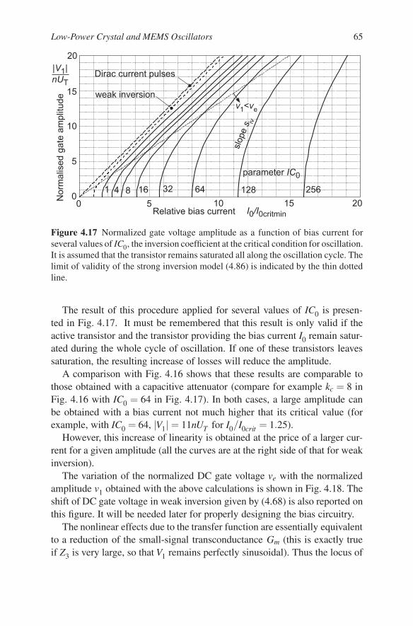
Low-Power Crystal and MEMS Oscillators 65
Figure 4.17 Normalized gate voltage amplitude as a function of bias current forseveral values of IC0, the inversion coefficient at the critical condition for oscillation.It is assumed that the transistor remains saturated all along the oscillation cycle. Thelimit of validity of the strong inversion model (4.86) is indicated by the thin dottedline.
The result of this procedure applied for several values of IC0 is presen-ted in Fig. 4.17. It must be remembered that this result is only valid if theactive transistor and the transistor providing the bias current I0 remain satur-ated during the whole cycle of oscillation. If one of these transistors leavessaturation, the resulting increase of losses will reduce the amplitude.
A comparison with Fig. 4.16 shows that these results are comparable tothose obtained with a capacitive attenuator (compare for example kc = 8 inFig. 4.16 with IC0 = 64 in Fig. 4.17). In both cases, a large amplitude canbe obtained with a bias current not much higher that its critical value (forexample, with IC0 = 64, |V1| = 11nUT for I0/I0crit = 1.25).
However, this increase of linearity is obtained at the price of a larger cur-rent for a given amplitude (all the curves are at the right side of that for weakinversion).
The variation of the normalized DC gate voltage ve with the normalizedamplitude v1 obtained with the above calculations is shown in Fig. 4.18. Theshift of DC gate voltage in weak inversion given by (4.68) is also reported onthis figure. It will be needed later for properly designing the bias circuitry.
The nonlinear effects due to the transfer function are essentially equivalentto a reduction of the small-signal transconductance Gm (this is exactly trueif Z3 is very large, so that V1 remains perfectly sinusoidal). Thus the locus of

66 4 Theory of the Pierce Oscillator
Figure 4.18 Variation of the DC component VG0 of gate voltage with the gatevoltage amplitude |V1| at stable oscillation. The shift ∆VG0 in weak inversion isshown in dotted line.
Zc(1)(Ic) follows the circular locus of Zc(Gm). For a given value of Rm, thevalue of pc is therefore independent of the amplitude.
As illustrated in the example of Fig. 4.11, this is not the case for strongernonlinear effects such as those due to the desaturation of the active transistor,or of the transistor delivering the bias current. In order to avoid those effects,the amplitude should be limited. This is best obtained by using an amplitudecontrol loop as will be described in Section 5.2.
4.3.3.5 Transistor Strictly in Strong Inversion
If the transistor is in strong inversion at the critical current for oscillation(Ispec I0crit ) then from (3.56):
I0crit = nUT
√IC0Gmcrit =
√IC0I0critmin. (4.78)
If the transistor remains strictly in strong inversion as the oscillation growsup, its drain current in saturation ID = IF can be expressed from (3.43) by
ID =Ispec
4(ve + v1 sinφ)2, (4.79)
Δ

Low-Power Crystal and MEMS Oscillators 67
where ve and v1 are the normalized voltages defined by (4.57). The funda-mental component of ID is then given by
|ID(1)|Ispec
=1
4π
∫ 2π
0(ve + v1 sinφ)2 sinφdφ =
vev1
2. (4.80)
The transconductance for the fundamental frequency, equal to the criticaltransconductance at stable oscillation according to (4.55), becomes
Gm(1) =|ID(1)||V1|
=veIspec
2nUT= Gmcrit . (4.81)
Solving for ve gives
ve =2nUT Gmcrit
Ispec=
2I0critmin
Ispec= 2
√IC0 (4.82)
where the last expression comes from the fact that, using (4.78):
I0critmin
Ispec=
I0crit
Ispec· I0critmin
I0crit=
IC0√IC0
=√
IC0. (4.83)
The normalized effective DC gate voltage ve is thus constant. But this is trueonly for
v1 < ve = 2√
IC0 (4.84)
otherwise the transistor enters weak inversion in the negative half periods ofgate voltage and (4.79) is no longer valid. This limit is shown by the dottedstrait line in Fig. 4.18. Notice that ve is already slightly descending belowthis limit, since the full model used for the calculation includes moderateinversion.
Returning to strict strong inversion, the DC component of drain current,that is the bias current I0 is given by
I0
Ispec=
18π
∫ 2π
0(ve + v1 sinφ)2dφ =
14
(v2
e +v2
1
2
)= IC0 +
v21
8. (4.85)
HenceI0
Icritmin=
I0
Ispec· Ispec
Icritmin=
√IC0 +
v21
8√
IC0
. (4.86)
By introducing the condition (4.84), the limit of validity becomes
v1 <34
I0
I0critmin. (4.87)
It is reported as a thin dotted line in Fig. 4.17.

68 4 Theory of the Pierce Oscillator
4.3.4 Energy and Power of Mechanical Oscillation
As explained in Section 2.4, the energy of mechanical oscillation is directlyrelated to the amplitude of motional current Im flowing in the motional im-pedance Zm. Considering the lossless case of Fig. 4.12, this current is relatedto the current I1 flowing through capacitor C1 by
I1 = (1+ jωC3Zm)Im. (4.88)
The real part of Zm is Rm, whereas at stable oscillation its imaginary partcompensates that of the circuit:
Im(Zm) = −Im(Zc(1)). (4.89)
If the circuit is not strongly nonlinear, Zc(1) may be replaced by Zc, the circu-lar locus of which is represented in Fig. 4.6. Now if Rm |Rn0|max (Km 1),this figure shows that Im(Zc) = 1/ jω(C3 +Cs). Thus, at stable oscillation:
Zm = Rm − 1jω(C3 +Cs)
, (4.90)
which, introduced in (4.88) yields
I1
Im=
(1− C3
Cs +C3+ jωC3Rm
)=
(Cs
Cs +C3+
jM
), (4.91)
or, for the amplitudes:
|I1||Im|
=
√(Cs
Cs +C3
)2
+1
M2 . (4.92)
Now the second term may usually be neglected since M 2, hence
|Im| ∼=(
1+C3
Cs
)|I1| =
(1+
C3
Cs
)ωC1|V1|. (4.93)
The amplitude of motional current depends on the gate voltage amplitude|V1| calculated in Section 4.3.3. The energy of mechanical oscillation is thenobtained by introducing this result in (2.23):
Em∼=
(1+
C3
Cs
)2 C21
2Cm|V1|2. (4.94)
It is proportional to the maximum energy stored in capacitor C1 and to the ra-tio C1/Cm. The power dissipated in the resonator can be obtained by applying(2.24), which gives
Pm =ωQ
Em∼=
(1+
C3
Cs
)2 ωC21
2QCm|V1|2 =
(1+
C3
Cs
)2 ω2C21Rm
2|V1|2. (4.95)

Low-Power Crystal and MEMS Oscillators 69
4.3.5 Frequency Stability
4.3.5.1 Introduction
The main feature to be optimized in a crystal oscillator, especially for time-keeping applications, is its frequency stability. Separated in three groups,the causes of degradation of this stability will be discussed in what follows,together with possible cures.
4.3.5.2 Resonator
The resonant frequency ωm of the resonator itself is not perfectly constant:a. Some variation with temperature is always present. As discussed in
Section 2.5, this variation depends on the type of resonator, which must beselected in accordance with the specifications of the oscillator.
b. There is no way to avoid some aging of the resonator after fabrication.Since the rate of aging usually decreases with time, it is possible to carry outsome pre-aging on the resonator before using it.
4.3.5.3 Nonlinear Effects in the Circuit
The amount of frequency pulling ps at stable oscillation was discussed inSection 3.2. As explained by Fig. 3.3, it is proportional to the imaginary partof Zc(1) (the circuit impedance for the fundamental frequency) at the stablepoint S.
Now, as illustrated by the example of Fig. 4.11(b), this imaginary part maybe strongly dependent on nonlinear effects. The nonlinear effects are them-selves dependent on various variables, including the supply voltage of thecircuits, the threshold voltage of the transistor and the ambient temperature.They must therefore be minimized to improve the frequency stability.
a. The nonlinear transfer function ID(VG) of the active transistor are thefirst to intervene when the amplitude increases. They limit the amplitude |V1|at the gate as illustrated in Fig. 4.17. To limit the resulting nonlinear effects,the bias current should not be much higher than its critical value, typically nomore than 10 or 20% above. The inversion coefficient IC0 of the transistorshould be selected in order to obtain the desired amplitude. Now, precisevalues of currents are hard to obtain in integrated circuits, and the criticalcurrent itself depends on many possibly variable parameters. Thus, the only

70 4 Theory of the Pierce Oscillator
possibility to control the amount of overdrive is to implement some kind ofvoltage amplitude regulation, as will be discussed in Section 5.2.
As was already explained in Section 4.3.2, the change of frequency dueto the nonlinear ID(VG) function is caused by intermodulation between har-monic components of the gate voltage. These are produced by harmoniccomponents of current flowing through the drain-to-gate impedance Z3,which can be reduced by increasing |Z3| (in particular by decreasing C3).
b. Nonlinearities in Z1 are due to the nonlinear dependency of the gatecapacitance on the gate voltage. Their effect can be reduced by implementinga sufficiently large value of C1 by means of a linear capacitor.
c. An important nonlinearity in Z2 occurs when the amplitude is so largethat the active transistor and/or the transistor delivering the bias current I0leave saturation in the peaks of drain voltage. Both transistors should be keptsaturated all along the oscillation cycle.
d. If |Z3| is large, as it should be, its possible nonlinearity should havenegligible effect on the frequency.
4.3.5.4 Variation of Linear Effects
If nonlinear effect on the frequency are made negligible, the amount of fre-quency pulling is equal to its value pc at the critical condition for oscillation.As illustrated by Fig. 4.4, pc is proportional to the imaginary part of thecircuit impedance Zc at the solution point A, where the real part of Zc com-pensates the motional resistance of the resonator (Re(Zc) = −Rm). Hence,any vertical displacement of A results in a variation of pc. Such a displace-ment may be due to several causes:
a. Even if the resonator has a very constant motional frequency, its qualityfactor may change, resulting in a change of motional resistance Rm. Theeffect of a variation of Rm is proportional to the slope of Zc at point A. Thisslope can be minimized by
- reducing C3 to increase the radius of the circle,- reducing the losses, in order to have the circular locus better centered on
the imaginary axis, and/or- reducing Rm (increasing Q).
b. Variation of the losses, that should therefore be- as small as possible- as constant as possible.

Low-Power Crystal and MEMS Oscillators 71
c. Variations of C1, C2 and/or C3, with an effect on pc given by (4.21).These 3 capacitors should therefore be kept as constant as possible. Thevoltage dependency of C1 due to the voltage dependent gate capacitance ofthe transistor can be minimized by implementing a sufficiently large valueof C1 by means of a linear capacitor. The same can be done to reduce thevoltage dependency of C2 due to the voltage dependent junction capacitanceat the drain node of the circuit.
Some capacitance variation may be due to mechanically unstable connec-tions between the circuit and the resonator.
The sensitivity of pc to capacitance variations can be obtained by differ-entiating (4.21). For Cs (series connection of C1 and C2) much larger than C3,this gives
dpc = −pc
(C2
C1(C1 +C2)dC1 +
C1
C2(C1 +C2)dC2 +
1Cs
dC3
). (4.96)
Thus, the effect of capacitance variations on the frequency of oscillation canbe reduced by reducing pc. But, as already explained in Section 4.2.2, thismay require a large increase of bias current, according to (4.26).
4.3.6 Elimination of Unwanted Modes
4.3.6.1 Introduction
As was explained in Section 2.2, all electromechanical resonators, in partic-ular the quartz resonator, have several possible modes of oscillation. Eachof them corresponds to a series resonant circuit in the complete equivalentcircuit of Fig. 2.2(a). We have explained in the same section that, once oscil-lation was obtained on one of these modes, no coupling could be producedby the circuit to the other modes.
Now, in all previous analyses, we have assumed that oscillation was ob-tained at the “wanted” mode and not at any other “unwanted” mode. Let usnow examine how this can be ensured.
Assuming that the circuit is designed to provide, for the desired mode, alarge margin factor Km (defined by (4.17)) and that losses are negligible, thecritical transconductance is given by (4.24) repeated here for convenience:
Gmcrit0∼= ω2Rm ·C1C2(1+C3/Cs)2. (4.97)
Now, the part after the dot is given by the circuit, and is at least the same forall the other modes (it could be larger for some modes if the corresponding

72 4 Theory of the Pierce Oscillator
value of Km would not be large, and (4.22) would have to be used instead of(4.24)).
On the contrary, the term ω2Rm (=ω/(QCm)) is specific to each mode.Hence (ω2Rm)w can be used to distinguish the wanted mode from allother unwanted modes, each of them being characterized by their value of(ω2Rm)u. Let us define
α (Gmcrit)u
(Gmcrit)w. (4.98)
For the lossless case, according to (4.97):
α = α0 (Gmcrit0)u
(Gmcrit0)w=
(ω2Rm)u
(ω2Rm)w. (4.99)
The wanted mode will be said to be more active than the unwanted mode ifα > 1 and less active if α < 1.
According to (3.55), the transconductance is proportional to the current ifthe transistor is in weak inversion (IC0 1), but only to the square root ofthe current if the transistor is in strong inversion (IC0 1). Hence:
(I0crit)u = α(I0crit)w in weak inversion (4.100)
(I0crit)u = α2(I0crit)w in strong inversion. (4.101)
4.3.6.2 Wanted Mode More Active Than Unwanted Modes (α > 1)
The wanted mode of oscillation is frequently the most active one. A safeprocedure is then to impose a fixed bias current I0 in the range
(I0crit)w < I0 < (I0crit)u. (4.102)
In practice however, this is only possible if α 1. Indeed, a small range ofpossible current would require a precise value of current that is not availablein an integrated circuit environment. Even if such a precise current wouldbe possible, its value would depend on Gmcrit and therefore on the value ofquality factor Q and on that of the various capacitors. Moreover, a small ratioI0/I0crit would provide only a small excess of negative resistance, resultingin a large start-up time constant τ0 given by (3.15), and thus in a very longstart-up time.
If the range of possible current is limited (α not much larger than 1),the best solution is to generate the bias current by means of an amplitude

Low-Power Crystal and MEMS Oscillators 73
regulator, as was explained in Section 3.4. Such a regulator provides a largeinitial bias current, which ensures a short start-up time. This bias currentdecreases when the amplitude increases, until equilibrium is reached.
Instead of regulating the current |Ics| = |Im| in the motional branch as inFig. 3.4, it is preferable to limit the voltage |V1| at the gate, which is relatedto |Im| by (4.93). This type of regulation is illustrated by Fig. 4.19 and willbe detailed in Section 5.2.
<
:*55
?
=? =?
=55 *
$?$
Figure 4.19 Regulation of the gate voltage amplitude.
In this example, Curve a represents the amplitude of oscillation |V1| atthe gate as a function of the bias current I0 for the wanted mode, as given byFig. 4.16 or 4.17. Curve b represents the bias current I0(|V1|) delivered by theamplitude detector. When the loop is closed, the system is expected to reachthe stable point Sw, with a bias current only slightly larger than its criticalvalue (I0crit)w. For the unwanted mode, the |V1|(I0) relationship is given byCurve c.
Let us assume that the start-up time constant of the unwanted mode isshorter than that for the wanted mode. Oscillation will start at this unwantedmode, and possibly reach the corresponding equilibrium point Su, with avalue of bias current just slightly larger than (I0crit)u. The transconductanceof the transistor is thus practically not affected by this oscillation, and re-mains larger than its critical value for the wanted mode. The amplitude ofthe wanted mode can therefore still grow up, thereby reducing I0 until thestable point Sw is reached. The bias current is then below its critical valuefor the unwanted mode, that can no longer be sustained. Oscillation at thewanted mode only is thus ensured.

74 4 Theory of the Pierce Oscillator
It is important to point out such a behavior is not ensured if I0 at pointSu is much larger than (I0crit)u, resulting in a strongly nonlinear behavior ofthe transistor. As a consequence, the remaining transconductance may not besufficient for starting up oscillation at the wanted mode. This is illustrated bythe results of simulations depicted in Fig. 4.20.
#µ
CE
Cµ4E
#µ
Cµ4E
55
5?5
5?5
55
?#'F
#F
?##&/
?##'3Ω ##/
#/
Figure 4.20 Possible dominance of the less active of two possible modes; in thesesimulation of start-up in a 0.18 µm process, the channel width is W = 50 µmwhereas the channel length L is changed from 2 to 4 µm. Notice that low valuesof quality factors (Qu < Qw = 1000) are used to facilitate the simulation.
In this example, the resonator has two possible modes (two series branchesin parallel). The wanted mode w has a resonant angular frequency ωw =2 · 105 s−1 with a motional inductance Lmw=250H, whereas Lmu=100H forthe unwanted mode u, giving ωu = 3.16 · 105 s−1. It is therefore less activethan mode w, in a ratio α = 2.5. The upper part of the figure shows that, fora channel length L = 2 µm of the active transistor, the motional current |Imw|of mode w remains zero (no oscillation at the wanted mode) whereas |Imu|stabilizes at about 2 µA. If L is increased to 4µm, the circuit become slightlyless nonlinear because the inversion coefficient in the peaks of drain currentis increased (from 0.26 to 0.49). As a result, oscillation at mode u does notprevent mode w to grow and to finally stay alone.

Low-Power Crystal and MEMS Oscillators 75
4.3.6.3 Effect of Losses
As discussed in Section 4.2.5, the main effect of losses is to increase the crit-ical transconductance Gmcrit . At a given frequency, these losses may alwaysbe represented by an additional component of conductance G1, G2 and/or G3in parallel with the capacitors. As long as they are not too large, the resultingincrease of Gmcrit is given by (4.45).
If the Gi remain independent of the frequency (as is the case if they are dueto real conductances in parallel), the critical transconductance is increased bythe same amount for all possible modes of oscillation. The relative differenceof critical transconductances is reduced and, according to (4.98), the valueof α becomes closer to unity. The potential problem illustrated by Fig. 4.20is worsened, and this kind of losses cannot help separating the wanted modefrom the unwanted one.
But each of the Gi can possibly be frequency dependent. The most simplecase is a resistance Ri in series with capacitance Ci. If (ωCiRi)
2 1, then
Gi∼= ω2C2
i Ri. (4.103)
The loss conductance is then increasing with the frequency, which may helpeliminating an unwanted mode, as discussed below.
4.3.6.4 Wanted Mode Less Active Than Unwanted Modes (α < 1)
This is a difficult situation. If the unwanted mode has a higher frequencythan the wanted mode, its overall activity may be reduced by introducing aresistance in series with C1 and/or C2. As given by (4.103), this will producean additional component of G1 and/or G2 that is proportional to ω2. Thiscomponent is therefore larger for the unwanted mode, which may push thevalue of α above unity.
An other way to analyze this solution is to consider the path of the mo-tional current for each mode as illustrated in Fig. 4.21. If C3 is sufficientlysmall to be negligible, most of the motional current of each resonator branchflows in the loop closed by capacitors C1 and C2. Hence, a resistor Rs insertedin this loop is approximately added to the motional resistors Rmw and Rmu.The effective activity ratio can therefore be approximated by
α ∼= ω2u (Rmu + Rs)
ω2w(Rmw + Rs)
, (4.104)
which is assumed to be smaller than unity for Rs = 0 (more active unwantedmode at higher frequency). This ratio will become larger than unity for

76 4 Theory of the Pierce Oscillator
?
?
?
ω?ω
Figure 4.21 Loss resistor Rs is the main loop of oscillation current.
Rs >ω2
wRmw −ω2u Rmu
ω2u −ω2
w=
1−α0
(ωu/ωw)2 −1Rmw. (4.105)
If α0 is close to unity or if the frequency ratio is large, then Rs Rmw andthe unwanted mode can be eliminated without too much effect on the wantedmode.
The situation is even more difficult if the unwanted mode is more activeand has a lower frequency than the wanted mode. This is the case if thewanted mode is an overtone.
One possible solution would be to exploit the nonlinear effects illustratedby Fig. 4.20. Indeed, in the upper part of the figure, the less active higher fre-quency mode dominates because it has a shorter start-up time constant. How-ever, this solution is not recommended because two possible stable modesof oscillation exist, and which one dominates depends on the initial condi-tions. For example, simulations show that, in the example of the figure withL = 2 µm, the more active low-frequency mode still dominates if the sup-ply voltage of the circuit is raised very slowly instead of being switched onabruptly.
There is no simple way to produce losses that increase when the frequencydecreases, but the unwanted mode can be avoided by inserting a parallel res-onant circuit tuned to its frequency in series with the source of the transistor.The unwanted mode will then be prevented if the (real) impedance at the res-onance is larger than 1/Gmcritu (where Gmcritu is the critical transconductancefor the unwanted mode). Furthermore, the capacitance of the resonant circuitshould be large enough to prevent source degeneration for the wanted mode.For the example of Fig. 4.20, this solution would require a capacitance of1nF, an inductance of 25mH and parallel resistance of 1MΩ, correspondingto a quality factor of 200, which is not realistic. In an integrated circuit en-

Low-Power Crystal and MEMS Oscillators 77
vironment, this solution is thus only applicable at high frequencies, and fora large ratio ωw/ωu.
4.4 Phase Noise
4.4.1 Linear Effects on Phase Noise
4.4.1.1 General Case
According to (3.30), the phase noise of the oscillator depends on the energyof oscillation Em, the quality factor Q of the resonator, and the frequency ofoscillation ω . It also depends on the noise excess factor γ of the circuit.
As defined by (3.23), this noise excess factor is the ratio between the spec-trum SV 2
nof the noise voltage Vn produced by the circuit to that of the thermal
noise of the motional resistance 4kT Rm. If Gi ωCi, losses can be neg-lected and this noise voltage can be calculated from the equivalent circuit ofFig. 4.22. The source of noise In is the channel noise of the transistor plus
Figure 4.22 Equivalent circuit of the Pierce oscillator for the calculation of thenoise voltage Vn.
additional noise delivered by the biasing current source. Assuming C3 C1and C2, the noise voltage can be expressed as
Vn =In
jωnC2 + GmC3/C1, (4.106)
where ωn is the frequency at which noise is considered.At frequencies close to the oscillation frequency ω , the spectral densities
are thus related by

78 4 Theory of the Pierce Oscillator
SV 2n
=SI2
n
(ωC2)2 +(GmC3/C1)2 =SI2
n
(ωC2)2
[1+
(Gm
MGmcrit0
)2] ∼=
SI2n
(ωC2)2 ,
(4.107)where the second expression has been obtained by introducing the factor ofmerit M defined by (2.9) through the relationship (4.24) between Rm andGmcrit0. Since M 1, the term between brackets is usually close to unity,thus the noise excess factor for very small amplitudes is
γ0 SV 2
n
4kT Rm
∼=SI2
n
4kT Rm(ωC2)2 (4.108)
4.4.1.2 Channel Noise of the Active Transistor
If the bias current were free of noise, the only source of In would be thechannel noise of the active transistor. Its spectral density given by (3.60) canbe introduced into (4.108). The noise excess factor is then given by
γ0∼=
γtnGmcrit
(ωC2)2Rm. (4.109)
Using again (4.24) to replace Rm by Gmcrit0, it becomes
γ0∼= γtn ·
C1
C2· Gmcrit
Gmcrit0. (4.110)
4.4.2 Phase Noise in the Nonlinear Time Variant Circuit
4.4.2.1 Introduction
As discussed in Section 3.7.2, the results obtained in the previous sectionare no longer valid when the amplitude increases, since the circuit becomesnonlinear and the noise becomes cyclostationary.
Neglecting the parallel capacitor C3, the phase noise can be analyzed bymeans of the equivalent circuit of Fig. 3.9 with Ci = C2. The cyclostationarynoise sources are functions of sin(φ + ∆φ ), where φ = ωt and ∆φ is thephase shift between the sinusoidal voltages V2 and V1.

Low-Power Crystal and MEMS Oscillators 79
An approximation of this phase shift can be calculated at the critical con-dition for oscillation from (4.34) and (4.45). As long as the condition (4.43)if fulfilled (small losses):
tan ∆φ ∼=1
ωC1
[Gmcrit0 + G1
(1+
C2
C1
)+ G3
C1 +C2
Cs
]. (4.111)
It is independent of a possible loss conductance G2.Now, because of the presence of C3 (or more generally Z3 between drain
and gate, some noise fed back through the transistor is added to the noisecurrent In of Fig. 4.22. This effect will be neglected, as was done in thelinear analysis.
4.4.2.2 Effect of the White Channel Noise in Weak Inversion
In weak inversion, the variation of drain current during each cycle of stableoscillation can be expressed by introducing (4.58) and (4.65) in (4.56). Withthe phase shift ∆φ , this yields
ID = I0critminv1
2IB1(v1)ev1 sin(φ+∆ φ). (4.112)
Thus, from (3.61) and (3.54), the cyclostationary drain noise current spec-trum is
α2i SI2
n= 2nkT Gmcrit
v1
2IB1(v1)︸ ︷︷ ︸S
I2n
ev1 sin(φ+∆ φ)︸ ︷︷ ︸α2
i
, (4.113)
where the first part is the spectrum SI2n
of a fictitious white noise currentmodulated by αi. According to (3.34), the squared RMS value of the effectiveimpulse sensitivity function (ISF) is then
Γ 2i (v1) = cos2 φα2
i =1
2π
∫ 2π
0cos2 φ · ev1 sin(φ+∆ φ)dφ (weak inversion).
(4.114)The phase noise spectrum is then obtained by introducing the above valuesof SI2
nand Γ 2
i in (3.33), which results in
Sφ 2n
= Sφ 2n 0
v1
IB1(v1)Γ 2
i (v1), (4.115)
where

80 4 Theory of the Pierce Oscillator
Sφ 2n 0 =
nkT Gmcrit
2(C2|V2|∆ω)2 ·C2m
C22
. (4.116)
is the phase noise spectrum for very small amplitudes. Referring to Fig. 3.9,C2|V2| may be replaced by |Im|/ω (even with a small phase shift, the amp-litude of the current is only very slightly affected). Thus, by introducing theexpression (4.24) of the lossless critical transconductance Gmcrit0 (with C3neglected):
Sφ 2n 0 =
nC1
2C2· Gmcrit
Gmcrit0· kT
Q2|Im|2Rm· ω2
∆ω2 . (4.117)
According to (3.29), this corresponds to an noise excess factor
γ0 =nC1
2C2· Gmcrit
Gmcrit0, (4.118)
which is identical to the value given by (4.110) and obtained by the linearanalysis, since γt = 1/2 in weak inversion. For larger amplitudes, γ growsproportionally to the noise spectrum contribution:
γ = γ0v1
IB1(v1)Γ 2
i (v1). (4.119)
This variation is plotted in Fig. 4.23 for several values of phase shift ∆φ .
∆φ #&'&
&
&
&
)**55
) >
+ ,&
&'
&
&'
)"
γ/γ
Figure 4.23 Phase noise excess factor in weak inversion.
The increase of γ with the amplitude depends on the phase shift ∆φ . Therewould be no increase with ∆φ = 0.
4.4.2.3 Effect of the White Channel Noise in Strong Inversion
The variation of the transconductance in strong inversion can be expressedby introducing in (3.56) the normalized variables ve and v1 defined by (4.57):

Low-Power Crystal and MEMS Oscillators 81
Gm = βUT (ve + v1 sin (φ + ∆φ)). (4.120)
In stable oscillation, the value of ve is independent of the amplitude, as in-dicated by (4.82). Hence βUT ve = Gmcrit , giving
Gm = Gmcrit(1+ mv sin (φ + ∆φ)), (4.121)
where
mv =v1
ve=
|V1|2nUT
√IC0
≤ 1 (4.122)
is the gate voltage modulation index. Thus, from (3.60), the spectrum of thecyclostationary drain current noise is
α2i SI2
n= 4γt kT nGmcrit︸ ︷︷ ︸
SI2n
(1+ mv sin(φ + ∆φ)︸ ︷︷ ︸α2
i
. (4.123)
The squared RMS value of the effective ISF is thus
Γ 2i (v1) =
12π
∫ 2π
0cos2 φ · (1+ mv sin(φ + ∆φ))dφ =
12. (4.124)
It is constant, hence the phase noise spectrum is independent of the phaseshift ∆φ and of the amplitude of oscillation. This is true as long as the tran-sistor remains strictly in strong inversion (i.e with mv ≤ 1). It can easily beshown that the corresponding noise excess factor is γ = γ0 given by (4.110).
4.4.2.4 Effect of the Flicker Noise in Weak Inversion
Using the approximation (3.62) of a noise voltage at the gate independent ofthe current, the resulting drain current noise spectrum is
α2i SI2
n=
Kf G2m
ωn=
Kf G2mcrit
ωn
(v1
2IB1(v1)
)2
︸ ︷︷ ︸Kfi/ωn
(ev1 sin (φ+∆ φ)
)2
︸ ︷︷ ︸α2
i
, (4.125)
since the transconductance is proportional to the drain current given by(4.112). The first part is the spectrum density Kf i/ωn of a fictitious stationaryflicker current noise source modulated by αi.
According to (3.34), the average value of the effective ISF is then
Γi = cosφ ·αi =1
2π
∫ 2π
0cosφ · ev1 sin (φ+∆ φ)dφ . (4.126)

82 4 Theory of the Pierce Oscillator
Now∫ 2π
0cos φ · ev1 sin (φ+∆ φ)dφ = sin (∆φ)
∫ 2π
0sinφ · ev1 sinφ dφ . (4.127)
Thus:Γi = sin(∆φ) · IB1(v1). (4.128)
The phase noise spectrum is obtained by introducing the above values ofKf i and Γi in (3.36), which yields
Sφ 2n
=(
GmcritCmv1
2C22 |V2|
)2
·Kf
∆ω3 · sin2 (∆φ). (4.129)
By introducing again the expression (4.24) of the lossless transconduct-ance Gmcrit0 (C3 neglected) and using the good approximation C2|V2| =C1|V1|, this results becomes
Sφ 2n
=(
Gmcrit
Gmcrit0
)2 (ω
2QnUT
)2
·Kf
∆ω3 · sin2 (∆φ), (4.130)
which is independent of the amplitude. Thus the flicker noise contribution tothe phase noise is independent of the amplitude, but depends on the phaseshift ∆φ . Remember that this results is obtained with the hypotheses of asinusoidal drain voltage and the noise model (3.62).
4.4.2.5 Effect of the Flicker Noise in Strong Inversion
Using the expression (4.121) of the transconductance, the noise current drainspectrum is
α2i SI2
n=
Kf G2m
ωn=
Kf G2mcrit
ωn︸ ︷︷ ︸Kfi/ωn
(1+ mv sin (φ + ∆φ))2
︸ ︷︷ ︸α2
i
. (4.131)
The average value of the effective ISF is thus
Γi = cosφ ·αi =1
2π
∫ 2π
0cosφ · (1+ mv sin(φ + ∆φ))dφ =
mv
2sin (∆φ).
(4.132)The phase noise spectrum is obtained by introducing the above values of Kf i
and Γi in (3.36):

Low-Power Crystal and MEMS Oscillators 83
Sφ 2n
=(
mvGmcritCm
2C22 |V2|
)2
·Kf
∆ω3 · sin2 (∆φ). (4.133)
This result is identical to (4.129), except that the normalized voltage v1 isreplaced by the modulation index mv = v1/(2
√IC0) (as defined by (4.122)).
For strong inversion, the result (4.130) is thus changed to
Sφ 2n
=(
Gmcrit
Gmcrit0
)2 (ω
4QnUT
)2
· 1IC0
·Kf
∆ω3 · sin2 (∆φ). (4.134)
For the same value of phase shift ∆φ , the noise spectrum is reduced by afactor 4IC0 compared to weak inversion.
4.4.2.6 Effect of the Noise in the Bias Current
The noise density associated with the bias current I0 is constant along the os-cillation cycle, thus αi = 1. As long as the hypothesis of a sinusoidal voltageV2 is valid, the effective ISF Γi is given by (3.34).
Hence, the average value of the effective ISF is zero and no flicker noise(or other low frequency noise) is transposed around the oscillation frequency.
Still according to (3.34), Γ 2i = 1/2. The phase noise produced by the white
noise content of the bias current of density SI2nb
is thus, from (3.33)
Sφ 2n
=SI2
nb
4(C2|V2|)2∆ω2 ·C2
m
C22
. (4.135)
Or, after replacing again C2|V2| by |Im|/ω and using (2.3) to replace Cm:
Sφ 2n
=SI2
nb
(2|Im|C2QRm∆ω)2 . (4.136)
According to (3.29), the phase noise excess factor due to bias noise is thus
γb =SI2
nb
4kT Rm(ωC2)2 . (4.137)
The comparison with (4.108) shows that, with the hypothesis of a sinusoidaldrain voltage V2, the circuits behaves linearly with repect to the noise of thebias current I0 (as could be expected).
Now if the saturated transistor delivering the bias current is controlledby a gate voltage that is free of noise at frequencies around the oscillation

84 4 Theory of the Pierce Oscillator
frequency, then SI2nb
is given by (3.60). Using the expression of the critical
transconductance Gmcrit0 of the lossless circuit and neglecting C3, (4.137)becomes
γb = γtnC1
C2· Gmb
Gmcrit0, (4.138)
where Gmb is the transconductance of the biasing transistor.This contribution to phase noise can thus be made negligible by having
this transconductance much lower than Gmcrit , by operating the biasing tran-sistor in strong inversion at an inversion coefficient much larger than IC0,and by filtering out the noise at its gate for frequencies around the oscillationfrequency.
4.5 Design Process
4.5.1 Design Steps
On the basis of what has been explained so far, the design of the core of aPierce oscillator should be done according to the following steps.
4.5.1.1 Selection of a Quartz Crystal or MEM Resonator
Several criteria should be considered, most of them imposed by the system.Most important are the desired frequency of oscillation and its acceptabledependency on temperature. Both have an impact on the type of resonator.For example, very low frequency is only possible with resonators oscillatingin flexural mode (possibly in the form of a tuning fork), but their temperaturedependency is quadratic, with a coefficient of about −4 ·10−8/C2. For veryhigh frequencies, a thickness mode is necessary, either shearing or expan-sion. Other criteria are cost, size, and aging properties. The quality factor Qshould be as high as possible, especially to ensure a low phase noise. A goodcircuit design can always take advantage of its high value.
Technical data published by commercial quartz crystal vendors alwaysinclude the frequency of oscillation ω and the motional resistor Rm (or atleast its maximum value). They do not always publish the third parameterneeded to characterize the series resonant circuit of Fig. 2.2, namely Q orCm. But they usually give the value of the “static capacitor” C0 across the

Low-Power Crystal and MEMS Oscillators 85
resonator measured as a dipole, defined by (2.1). The value of C12 can thus beobtained since the values of C10 and C20 are known, measurable or negligible.
Knowing C12, the value of Cm is always smaller than C12/100 (because ofthe limited piezoelectric coupling coefficient of quartz). It is usually rangingbetween 0.1 and 0.25 this limit. Practical numerical values range from 0.5 to5fF for quartz resonators.
The value of Cm might be smaller for MEM resonators, due to the smallvalue of the electrical capacitance given by (2.27). The motional resistanceRm would then be higher and the parallel capacitance C3 would be dominatedby parasitic capacitances, there by reducing the margin factor Km definedby (4.17). In the extreme case, oscillation might not be possible with thePierce oscillator, and alternative architectures like those discussed in Chapter6 might be needed.
4.5.1.2 Choice of Circuit Capacitances C1 and C2 and Estimation of C3
As given by (4.21), the values of C1 and C2 essentially control the amountof frequency pulling pc by the circuit. If pc is increased, the frequency ofoscillation moves away from the intrinsic mechanical resonant frequency ofthe resonator and becomes more dependent on the sustaining circuit. Fre-quency stability is then degraded. If pc is reduced, (4.26) shows that the crit-ical transconductance Gmcrit is increased, resulting in an increase of powerconsumption. The same formula shows that for a given amount of pulling,Gmcrit is minimum for C1 = C2.
As explained in Section 4.2.2, C1 and C2 must be large enough with re-spect to C3 to ensure a maximum value of negative resistance much largerthan the motional resistance Rm (Km 1). This is to minimize the effect ofvariations of Rm on the frequency of oscillation.
If the source of the transistor is grounded, C3 is usually dominated by theintrinsic parallel capacitance C12 of the resonator plus the drain-to-source ca-pacitance of the transistor (that must be pre-estimated). If the drain is groun-ded, C10 (or C20) is added (see Fig. 2.2) and C3 may become much larger.
It should be pointed out that many crystal vendors do not provide the valueof motional capacitor Cm, but specify instead the value of load capacitancefor the specified frequency of oscillation (thereby imposing the value of pc).This load capacitance is the total equivalent capacitance connected in parallelwith the physical resonator. Thus, for the Pierce oscillator:
CLoad C3 +Cs −C0, (4.139)

86 4 Theory of the Pierce Oscillator
If frequency adjustment is obtained by adjusting the value of Cs, bestwould be to maintain C1 = C2. In practice, only C1 or C2 is adjusted, de-pending on which of the 3 nodes in grounded in the final implementation.
4.5.1.3 Calculation of Pulling and Series Resonant Frequency
Knowing Cm, C1, C2 and C3, the frequency pulling pc at the critical conditionfor oscillation can be calculated by (4.21), assuming a negligible effect oflosses. In a good design, this effect as well as that of nonlinearities should bekept negligible. Hence the pulling ps at stable oscillation will be very closeto this value. Knowing the specified frequency of stable oscillation fs, theexact (series) resonant frequency fm to be specified for the resonator is givenby
fm ωm
2π= fs(1− pc). (4.140)
4.5.1.4 Calculation of the Minimum Start-up Time Constant and of theCorresponding Transconductance
The maximum possible negative resistance |Rn0|max is given by (4.11). Theminimum start-up time constant is then calculated by (3.15), and (4.13) givesthe value Gmopt of the transconductance for which it is obtained.
4.5.1.5 Calculation of the Critical Transconductance and MinimumCritical Bias Current
Assuming that K2m is duly much larger than unity, the lossless critical transcon-
ductance Gmcrit0 is given by (4.24) (since the values of ω and Rm are alwaysavailable from the resonator data sheet).
After verification of the condition (4.43) with the expected values of lossconductances, the increase of critical transconductance ∆Gmcrit due to theseslosses can be calculated by (4.45) and added to its lossless value Gmcrit0.
The minimum value of critical current Icritmin, which would be obtainedwith the transistor operated in weak inversion, can be calculated by (4.64).

Low-Power Crystal and MEMS Oscillators 87
4.5.1.6 Choice of the Amplitude of Oscillation |V1| at the Gate
If the amplitude of oscillation is too small, the output signal has to be amp-lified to be used in the system. As will be shown later, the input admittanceof the amplifier may have a real part proportional to its voltage gain, whichadds losses in the oscillator. Moreover, the input referred noise of the ampli-fier is transformed into a component of phase noise. Furthermore, accordingto (4.94), the energy of oscillation is proportional to |V 2
1 |. Thus, according to(3.30), a too small value of |V1| may result in an unacceptable level of phasenoise around the frequency of oscillation.
If the amplitude of oscillation is too large, the power dissipated in theresonator ( given by (4.95)) can exceed the acceptable limit, resulting in ex-cessive aging or even breaking of the resonator. Moreover, a large amplitudeof oscillation requires a large value of supply voltage to maintain the activetransistor in saturation, in order to avoid additional losses and a degradationof frequency stability.
4.5.1.7 Calculation of Power
The power dissipated in the resonator is obtained by (4.95). This is alwayspossible since ω and Rm are always known. The result must then be com-pared with the maximum acceptable value, as given by the vendor.
4.5.1.8 Choice of the Amount of Overdrive
As illustrated by Fig. 4.17 (or by Fig. 4.16), the overdrive current ratioI0/I0crit necessary to obtain a given amplitude can be controlled by IC0, theinversion coefficient of the transistor at I0crit (or by kc, the attenuation of thecapacitive divider of Fig. 4.16).
A small amount of overdrive should be chosen to minimize the nonlineareffects. This is needed to reduce the risk of oscillation on an unwanted mode,as discussed in Section 4.3.6. It is also needed for a good frequency stability,as explained in Section 4.3.5.3a.
But Fig. 4.17 also shows that the larger the overdrive, the smaller the biascurrent necessary to obtain a given amplitude. Indeed, the absolute minimumis obtained when the transistor is weak inversion.

88 4 Theory of the Pierce Oscillator
4.5.1.9 Calculation of Critical Current, Bias Current and SpecificCurrent of the Transistor
Once the choice of IC0 has been made, the critical current of oscillation (biascurrent for zero amplitude) is obtained from (4.73) and (4.64):
I0crit = I0critmin
√IC0
1− e−√
IC0
. (4.141)
It is simply kc · I0critmin in weak inversion with a capacitive attenuator as inFig. 4.15.
The bias current needed to obtain the expected amplitude is then be ob-tained by inspecting Fig. 4.17 (or Fig. 4.16).
Knowing I0crit and IC0, the specific current of the transistor is obtainedfrom the definition (4.72) of IC0:
Ispec = I0crit/IC0. (4.142)
4.5.1.10 Calculation of the Active Transistor
The width-to-length ratio of the active transistor W/L is obtained from thedefinition (3.41) of Ispec.
To avoid additional losses due to the output conductance Gds, the intrinsicvoltage gain of the transistor given by (3.58) should be much larger thanunity. Thus, the channel length L should be more than the minimum possible,to ensure an acceptable value of VM .
Knowing the values of L and W , the gate capacitance can be can be cal-culated to verify that it is only a small fraction of C1, since it is voltagedependent.
The voltage-dependent drain capacitance is proportional to W , and shouldonly be a small fraction of C2.
The drain to gate capacitance is also proportional to W . It must be includedin the value of C3.
4.5.1.11 Calculation of Energy and Phase Noise
The energy of oscillation in the resonator is given by 4.94. Its calculationrequires the value of Cm or an approximation of it.
The phase shift ∆φ is obtained from the approximation (4.111).

Low-Power Crystal and MEMS Oscillators 89
In strict strong inversion, the noise excess factor due to the active transistoralone is just the small amplitude value given by (4.110). In weak inversion, itincrease with the amplitude as expressed by (4.119). It should be augmentedto include the noise component of the bias current as discussed in Section(4.4.2.6). The phase noise spectrum due white noise sources can then becalculated by (3.30).
The component of phase noise due to the flicker noise of the active tran-sistor is calculated by (4.130) in weak inversion, and by (4.134) in stronginversion.
Overall, and due to the very large values of quality factor Q, the phasenoise of the quartz oscillator itself is negligible in many applications.
4.5.1.12 Final Complete Design
The next design steps will be to select which of the three points of the basiccircuit is grounded, to define a bias scheme (including the very importantamplitude limitation) and to design the output circuitry that is usually anamplifying stage. These steps will be discussed in Chapter 5.
4.5.2 Design Examples
The design process summarized in the previous section will now be illus-trated by two examples with two different quartz resonators. Their charac-teristics are given in Table 4.1.
The quartz of Example 1 is a typical miniaturized wristwatch tuning fork.Its flexural mode in X+5 cut gives a quadratic temperature behavior (3.5 ·10−8/C2, with a maximum around 25C). The quartz of Example 2 is ahigh frequency AT cut inverted mesa, with a cubical temperature behavior. Ithas a lower minimum value of quality factor Q and oscillates in fundamentalmode.
Table 4.2 gives the main data of the process to be used in these examples.It is a typical 0.18 µm process. Note that, except for the threshold VT0, onlythe nominal values are given; the final design should be checked for the worstcase by computer simulation.
The successive design steps of Section 4.5.1 are presented in Table 4.3.The quartz data do not provide the value of C12 defined in Fig. 2.2(a).
Instead, they only give the lumped parallel capacitance C0 defined by (2.1)(quartz considered as a dipole). To consider the worst case in Step 2, we

90 4 Theory of the Pierce Oscillator
Param. Example 1 Example 2 Unitexact osc.frequency fs 32768.00 50.00000 ·106 Hzapproximation ω 2.06 ·105 3.14 ·108 1/smax. resistance Rm 42 ·103 100 Ωmotional capacitance Cm 2.1 ·10−15 2.7 ·10−15 Fmin. quality factor Q 55100 11800parallel capacitance C0 0.9 ·10−12 2.4 ·10−12 Fmax. power Pmax 10−6 10−4 W
Table 4.1 Quartz crystal data.
parameter N-channel P-channel unitkT 4.16 ·10−21 4.16 ·10−21 JUT 26 ·10−3 26 ·10−3 Vn 1.30 1.35Ispec (for L = W ) 0.50 ·10−6 0.20 ·10−6 AVT0 0.45±0.1 0.45±0.1 VCox 8.50 ·10−3 8.50 ·10−3 F/m2
Cd/W 0.90 ·10−9 1.05 ·10−9 F/mCgd/W 0.36 ·10−9 0.33 ·10−9 F/mVM/L 30 ·106 40 ·106 V/mWLKf 2 ·10−22 m2V2
Table 4.2 Process data.
assume that C12 =C0 to evaluate the value of C3. Only a very small additionalcapacitor due to interconnects is assumed for the more critical high frequencyquartz.
Step 3 assumes that the amount of pulling ps in stable oscillation is notmodified by losses or by nonlinear effects, hence ps = pc. It provides theexact value of the resonant frequency fm.
The maximum negative resistance obtained in Step 4 is much larger thanRm for Example 1. It is sufficiently larger (K2
m = 20.7 1) for Example 2 tovalidate the approximations of pc by (4.21) and of Gmcrit0 by (4.24). Fromthe values obtained for τ0min, the minimum start-up times (ranging between7τ0min and 15τ0min) are 0.16 to 0.35 s and 0.15 to 0.32 ms. These values willbe larger if the transconductance at start-up is smaller (or larger) than thecalculated value of Gmopt .
In Step 5, estimated values of loss conductances are introduced. G1 ac-counts for the load by the output amplifier. G2 is essentially the output con-ductance of the saturated transistor and that of the driving current source. G3will be mainly due to the device biasing the gate. All these value will have

Low-Power Crystal and MEMS Oscillators 91
to be verified during the final design stage, and corrected if necessary. Theincrease of critical transconductance ∆Gmcrit is calculated by the approxim-ation (4.45) after verification of the condition (4.43).
In Step 6, the amplitude of oscillation is chosen sufficiently low to be com-patible with a supply voltage below 1.5V. For Example 2, it is also limitedto maintain the power Pm dissipated in the resonator (Step 7) below its max-imum acceptable value Pmax. The drain voltage amplitude |V2| is obtained by(4.35).
The choice of the inversion coefficient IC0 is made in Step 8. In Example1, the noise is not critical and the risk of exciting unwanted overtones issmall. Hence, a reasonably large overdrive is acceptable, and IC0 = 1 ischosen to achieve the minimum possible bias current. The transistor is thusapproximately in weak inversion.
Nonlinear effects must be limited in Example 2, essentially to minim-ize the phase noise. The choice is then IC0 = 64, resulting in an overdriveI0/I0crit = 1.078, as calculated in Step 9.
In Step 9, the critical current I0crit is calculated by (4.141) and the biascurrent I0 is obtained from Fig. 4.17 (or calculated by (4.86) for Example 2).
In Step 10, a long channel length L is chosen for Example 1, to render theoutput conductance Gds totally negligible. The length is reduced in Example2 to avoid a too large width W . As a consequence, the value of Gds is themain part of G2. Calculation of the various (voltage-dependent) capacitorsof the transistor show that they are all negligible with respect to C1, C2 andC3.
In Step 11, the noise excess factor γ is equal to its small amplitude valueγ0 in strong inversion (Example 2). It does not include the noise contributionof the current source I0. But even if γ is increased by a factor 10, therebyincreasing the noise by about 10dB, the phase noise remains very low.
The noise included in I0 is not modulated by the active transistor. Henceits low-frequency noise content is not shifted around fs.
Notice that the resulting phase noise is expressed in dBc/Hz (decibel rel-ative to the carrier) for ∆ f = 1kHz. With negligible amplitude noise, this isabout equivalent to radian2/Hz.

92 4 Theory of the Pierce Oscillator
step variable Example 1 Example 2 unit ref.2 C1 20 ·10−12 15 ·10−12 F
C2 20 ·10−12 15 ·10−12 FC3 2.0 ·10−12 2.6 ·10−12 FCs 10 ·10−12 7.5 ·10−12 F (4.9)
3 pc 87.5 ·10−6 134 ·10−6 (4.21)fm 32765.13 49.99332 ·106 Hz (4.140)
4 |Rn0|max 1.01 ·106 455 Ω (4.11)Km 24.1 4.55 (4.17)τ0min 23.2 ·10−3 21.2 ·10−6 s (3.15)Gmopt 49.4 ·10−6 36.6 ·10−3 A/V (4.13)
5 Gmcrit0 1.03 ·10−6 4.03 ·10−3 A/V (4.24)G1 0.10 ·10−6 0.20 ·10−3 A/VG2 0.01 ·10−6 0.20 ·10−3 A/VG3 0.10 ·10−6 0.20 ·10−3 A/V∆Gmcrit 0.51 ·10−6 1.20 ·10−3 A/V (4.45)Gmcrit 1.54 ·10−6 5.23 ·10−3 A/V (4.39)I0critmin 51.9 ·10−9 0.177 ·10−3 A (4.64)
6 |V1|/nUT 4.00 6.00|V1| 135 ·10−3 203 ·10−3 V|V2| 145 ·10−3 309 ·10−3 V (4.35)|V3| 276 ·10−3 472 ·10−3 V (4.37)
7 Em 2.51 ·10−9 3.11 ·10−9 J (4.94)Pm 9.37 ·10−9 82.8 ·10−6 W (4.95)
8 IC0 1 64I0/I0critmin 2.70 8.6 Fig. 4.17
9 I0crit 82.1 ·10−9 1.41 ·10−3 A (4.141)I0 140 ·10−9 1.52 ·10−3 AIspec 82.1 ·10−9 22.1 ·10−6 A (4.142)
10 W/L 0.164 44.2 (3.41)L 6.00 ·10−6 1.00 ·10−6 mW 0.985 ·10−6 44.2 ·10−6 mVM 180 30 VGds 0.78 ·10−9 50.6 ·10−6 A/V (3.57)Cg 50 ·10−15 376 ·10−15 FCd 0.88 ·10−15 39.8 ·10−15 FCgd 0.36 ·10−15 15.9 ·10−15 F
11 ∆φ 0.376 0.837 rad (4.111)γ0 0.973 1.12 (4.110)γ 1.31 Fig.4.23SΦ2
n 1/ f 2 at 1k -187 -150 dBc/Hz (3.30)
SΦ2n 1/ f 3 at 1k -189 dBc/Hz (4.130)
SΦ2n 1/ f 3 at 1k -140 dBc/Hz (4.134)
Table 4.3 Design calculations.

Chapter 5Implementations of the PierceOscillator
5.1 Grounded-Source Oscillator
5.1.1 Basic Circuit
Grounding the source of the active transistor results in the basic oscillatorcircuit depicted in Fig. 5.1. Transistor T2 is part of a current mirror thatdelivers the bias current I0 to the active transistor T1. The latter is maintainedin active mode by a resistor R3 that forces the DC component VD0 of the drainvoltage VD to be equal to the DC component VG0 of the gate voltage VG (sinceno current is flowing through R3).
:
;
<
;
>
>;
Figure 5.1 Basic grounded source oscillator.
E. Vittoz, Low-Power Crystal and MEMS Oscillators: The Experience of Watch Developments,Integrated Circuits and Systems, DOI 10.1007/978-90-481-9395-0_5,
93
© Springer Science+Business Media B.V. 2010

94 5 Implementations of the Pierce Oscillator
To avoid unnecessary losses, both transistor must remain saturated allalong the oscillation cycle.
If T1 is in weak inversion, it remains saturated as long as VD > 5UT , ac-cording to (3.46). Since VDmin = VD0 − |V2|, the minimum acceptable valueof threshold voltage can be expressed as
VT0 > 5UT + |V2|− (VD0 −VT0), (5.1)
where (VD0 −VT 0) is given by (4.68) for VD0 = VG0. The drain amplitude|V2| is related to the gate amplitude |V1| by (4.35). Some additional marginshould be provided to account for nonlinear effects that result in slightlylarger negative half periods of drain voltage.
For T1 is in strong inversion, the minimum value of drain voltage ensuringsaturation is given by (3.47). By introducing the DC components VG0 and VD0and the complex voltages V1 and V2 at the gate and at the drain, this conditionbecomes
VT 0 > |V1 −nV2|+VG0 −nVD0. (5.2)
For VD0 = VG0, it may be rewritten to express the minimum acceptablethreshold voltage:
VT 0 >1n[|V1 −nV2|− (n−1)(VG0 −VT0)]. (5.3)
The first term in the square parenthesis can be related to |V1| by using (4.35):
|V1 −nV2| = |V1|√
(nG1 + G2 + nGmcrit)2 + ω2(nC1 +C2)2
G22 +(ωC2)2 . (5.4)
The value VG0 −VT 0 for a given value of AC amplitude |V1| can be obtainedfrom Fig. 4.18 or from (4.82) for strict strong inversion. To ensure that theactive transistor remains saturated along the whole oscillation cycle, the min-imum threshold guaranteed for the process should fulfill condition (5.3). Ifthis condition is not fulfilled, the circuit should be modified to obtain a DCcomponent of drain voltage larger than VG0, as will be discussed in Section5.1.6.
For a given amplitude of oscillation |V2|, the minimum value of supplyvoltage VB is limited by the need to maintain the P-channel biasing transistorT2 in saturation:
VB > VD0 + |V2|+VD2sat , (5.5)
where VD2sat is the saturation drain voltage of T2 given by (3.47) (withVS = 0) if it is in strong inversion. It has a minimum value given by (3.46)

Low-Power Crystal and MEMS Oscillators 95
obtained in weak inversion. Hence, if its width does not become too large,this transistor should have a specific current larger than the bias current I0 toreduce the minimum value of VB. But, according to (4.138), the noise con-tribution of T2 is then no longer negligible. The drain amplitude |V2| is re-lated to the gate amplitude by (4.35) and the DC component of drain voltageVD0 = VG0 can be found in Fig. 4.18, using the maximum value of VT 0 forthe process considered.
5.1.2 Dynamic Behavior of Bias
If the bias current I0 is constant, then the DC component of drain current ID0has the same value. But if there are variations of I0, they are not followed im-mediately by ID0. Let us consider the equivalent circuit the oscillator drivenby small variations of the bias current, as shown in Fig. 5.2. δ I0 and δ ID0
δ
δ
Figure 5.2 Calculation of the bias transfer function.
are now complex variables representing small variations of I0 and ID0. The(angular) frequency Ω of these variations is supposed to be much smallerthan ωm, hence the motional impedance can be neglected (since Cm C1).It can easily be shown that
δ ID0
δ I0=
GmZ1Z2
Z1 + Z2 + Z3 + GmZ1Z2
, (5.6)
where Gm is the average value of transconductance along each oscillatorycycle. It has the value
Gm =I0
nUT(in weak inv.) and Gm = Gmcrit (in strict strong inv.), (5.7)
since it is proportional to the drain current in weak inversion and varies lin-early with the gate voltage in strong inversion.

96 5 Implementations of the Pierce Oscillator
Calculating (5.6) for the general case with real and imaginary parts ofthe impedances would result in a complicated expression, so it should becomputed numerically. But let us consider lossless capacitive impedancesZ1,Z2 (as in the example of Fig. 5.1), and neglect C3, thus Z3 = R3. Thisexpression becomes, in the s-domain
δ ID0
δ I0=
Gm
s2C1C2R + s(C1 +C2)+ Gm. (5.8)
For GmR3 (C1 +C2)2/(C1C2), the roots of the denominator are conjugate
complex, thus this expression can be rewritten as
δ ID0
δ I0=
Ω 20
s2 + sΩ0/Qb + Ω 20
. (5.9)
This transfer function has a resonant peak at frequency
Ω0 =
√Gm
R3C1C2(5.10)
In stable oscillation, Gm ≥ Gmcrit0, hence by introducing the expression(4.24) of Gmcrit0 (and neglecting C3), (5.10) becomes
Ω0 ≥ ωm
√Rm
R3, (5.11)
showing that the bias resistance R3 must be much larger than the motionalresistance Rm to obtain a resonant frequency of the bias circuit much lowerthan the frequency of oscillation.
The quality factor of this resonant circuit is
Qb =
√GmR3C1C2
(C1 +C2)2 =√
GmR3/4︸ ︷︷ ︸
for C1=C2
. (5.12)
So, without C3 the resonant peak could be very large, since R3 1/Gm tolimit the loss conductance G3. However, C3 strongly attenuates this peak assoon as its impedance at Ω0 is comparable to R3, which occurs if
C3∼=
√C1C2
GmR3
=Cs
Qb. (5.13)

Low-Power Crystal and MEMS Oscillators 97
so the higher the peak without C3, the more it is attenuated by C3. For ex-ample, with C1 =C2 and C3 =C1/10, the maximum peak is only 1.43 and oc-curs for GmR3
∼= 30 (where it would be 2.74 with C3 = 0 according to (5.12)).For C3 = C1/100, the maximum peak is 3.62 and occurs for GmR3
∼= 200(where it would be 7.07 with C3 = 0 ). Thus, with usual values of C3/C1,the peak is never very large. However, just above the peak frequency, thephase always reaches at least 90 degrees, which may have consequences onthe stability of an amplitude regulating loop, as will be seen further.
5.1.3 Dynamic Behavior of Oscillation Amplitude
For a constant DC component of drain current ID0 = I0, stable oscillationis reached with a gate amplitude |V1| as plotted in Fig. 4.17 (or Fig. 4.16).At this point the negative resistance Rn produced by the circuit compensatesexactly the motional resistance Rm of the resonator, and the time constant ofgrowth (or decay) τ defined by (3.3) is infinite.
Now, if at some time ID0 differs from this stable point by an amountδ ID0(t), the instantaneous value of amplitude will depart by an amountδ |V1|(t) from its stable value, as illustrated by Fig. 5.3.
δ|5
:*
;9
δ;
;#
δ"#δ;δ|5%
#
δ
δ
Figure 5.3 Calculation of the dynamic behavior of the oscillation amplitude.
As shown by the figure, this produces an instantaneous excess of currentδ Iex (that would tend to zero if δ ID0(t) would remain constant). Since allthese variables are time dependent, we can express them in the s-domain as:

98 5 Implementations of the Pierce Oscillator
δ Iex = δ I0 −δ |V1|/Riv (5.14)
where resistance Riv is the slope of the |V1|(I0) curve corresponding to stableoscillation. According to (4.55), this curve is the locus of Gm(1) = Gmcrit ,where Gm(1) is the effective transconductance including the effect of nonlin-earity of the transistor. The small excess current δ Iex produces an increase oftransconductance δGm(1), thus in the s-domain:
δGm(1) = k1δ Iex, (5.15)
where
k1 dGm(1)
dIex(5.16)
This increase of Gm(1) is the same as what would be obtained by an increaseδ I0crit of the critical transconductance, as illustrated by the curve in inter-rupted line. Since Gm(1) = Gm at Iocrit , the coefficient k1 can therefore beexpressed as
k1 =dI0crit
dIex· dGm
dID|ID=I0crit
=I0crit
I0· 1
2nUT
(1− e−
√IC0√
IC0
+ e−√
IC0
)(5.17)
by using expression (3.55) of the transconductance Gm. In weak inversion,I0/I0crit is given by (4.65) and IC0 1; (5.17) then becomes
k1 =2IB1(v1)|V1|IB0(v1)
(weak inversion) (5.18)
It must be remembered that Gm(1) = Gmcrit = Gmcrit0 +∆Gmcrit is the valueof transconductance needed to produce a negative resistance Rn equal themotional resistance −Rm. Then, if the increase of critical transconductance∆Gmcrit due to losses is constant, from (4.24):
k2 − dRn
dGm(1)=
Rm
Gmcrit0=
1ω2C1C2(1+C3/Cs)2 . (5.19)
Thus, the excess current δ Iex produces a net excess of negative resistancegiven by
δRn =dRn
dGm(1)·
dGm(1)
dIexδ Iex = −k1k2δ Iex (5.20)
The time constant τ given by (3.3) is then no longer infinite but, by introdu-cing (5.20) and (5.14)

Low-Power Crystal and MEMS Oscillators 99
1τ(s)
=δRn
−2Lm=
k1k2
2Lm
(δ I0 −
δ |V1|Riv
), (5.21)
where all variables are in the s-domain. The exponential growth of gatevoltage amplitude can be expressed in the time domain as
d(δ |V1|)dt
=|V1|τ
, (5.22)
which becomes, in the s-domain
sδ |V1| =|V1|τ(s)
= Kiv
(δ I0 −
δ |V1|Riv
), (5.23)
where
Kiv =k1k2|V1|
2Lm=
k1k2ω2Cm|V1|2
. (5.24)
Solving (5.23) for δ |V1| gives low-pass the transfer function for the amp-litude of oscillation
δ |V1|δ ID0
=Kiv
s+ Ωciv, (5.25)
whereΩciv = Kiv/Riv (5.26)
is the cut-off frequency. The differential resistance Riv is related to the slopesiv of the normalized function of Fig. 4.17 (or Fig. 4.16) by
Riv = siv/Gmcrit . (5.27)
The expressions (5.17) of k1 and (5.19) of k2 can be introduced in (5.24),which gives
Kiv =|V1|
4nUT· I0crit
I0· Cm
C1C2(1+C3/Cs)2 ·(
1− e−√
IC0√IC0
+ e−√
IC0
), (5.28)
where the term in parenthesis changes from 2 in weak inversion to 1/√
IC0in strong inversion. For the lossless case, Gmcrit = Gmcrit0 = Rm/k2 accordingto (5.19). The cut-off frequency can then be expressed from (5.26) as
Ωciv =ω
4Qsiv· |V1|
nUT· I0crit
I0·(
1− e−√
IC0√IC0
+ e−√
IC0
)(lossless case).
(5.29)

100 5 Implementations of the Pierce Oscillator
It is proportional to the frequency of oscillation and inversely proportionalto the quality factor Q of the resonator. The amplitude of oscillation followsthe variations of the drain current for frequencies lower than Ωciv, with thetransresistance Riv. Beyond this frequency, the transfer function is that of anintegrator Kiv/s and the variations are attenuated. However, they are shiftedby 90 degrees, which may endanger the stability of an amplitude regulatingloop. As can be seen in (5.28), this integrating behavior does not depend onthe frequency of oscillation nor on the quality factor of the resonator.
5.1.4 Design Examples
Table 5.1 shows the values obtained for the implementation of the two ex-amples introduced in Section 4.5.2 (Tables 4.1 and 4.2), using the resultsof Table 4.3. For the calculation of the minimum value of the N-channelthreshold ensuring saturation of the active transistor, weak inversion has beenassumed for Example 1 with VDsat = 5UT , and strong inversion for Example2. Both results are lower than the minimum value of 0.35V guaranteed forthe process.
To minimize the value of supply voltage VB in Example 1, the bias tran-sistor T2 is operated at an inversion coefficient IC2 = 1 for which a valueof VDsat =150mV is assumed. The minimum supply voltage is then only0.86V in the worst case of maximum threshold. Such a low value of IC2would have required an excessively large transistor (W =2.3mm) in Example2. Therefore, the inversion coefficient has been increased to 10, with the res-ult of an increase of saturation voltage. Combined with the large inversioncoefficient of the active transistor and with the larger amplitude of oscilla-tion, it increases the minimum value of VB to 1.62V in the worst case. Ofcourse, the oscillator would still works under this limit, but the amplitude ofoscillation would be limited by losses due to the output conductance of T2,with the negative consequences discussed in Section 4.3.5.
Even if the gate voltage of the biasing transistor T2 is free of noise, thecontribution γb of the bias current noise is not negligible. It increases thephase noise by 2dB in Example 1 and 4dB in Example 2.
Sizing the bias transistor is easy in Example 1. In Example 2, the channellength L has been selected as short as possible while keeping a value ofoutput conductance Gds smaller than the estimated value of G3. Becauseof the large current, a very wide transistor is however needed to limit theinversion coefficient at a large value of current. For both examples, the added

Low-Power Crystal and MEMS Oscillators 101
variable Example 1 Example 2 unit ref.|V1 − nV2| 319 ·10−3 561 ·10−3 V (5.4)VT0min 321 ·10−3 307 ·10−3 V (5.1),(5.3)IC2 1.00 10.0 V choiceVD2sat 150 ·10−3 200 ·10−3 V (3.46),(3.47)VBmin 0.86 1.62 V (5.5)Gmb = Gm2 2.52 ·10−6 13.1 ·10−3 A/V (3.55)γb 1.66 2.93 (4.138)γ0 + γb 2.97 4.05SΦ2
n 1/ f 2 at 1kHz -185 -146 dBc/Hz (3.30)
Ispec2 1.40 ·10−7 1.52 ·10−4 A (3.45)W2/L2 0.7 760 (3.41)L2 4 ·10−6 3 ·10−7 m choiceW2 2.8 ·10−6 228 ·10−6 mVM2 160 12 ·10−6 VGds2 0.88 ·10−9 0.13 ·10−3 A/V (3.57)Cd2 2.94 ·10−15 239 ·10−15 FCgd2 0.92 ·10−15 75.2 ·10−15 FR3 1.00 ·107 5.00 ·103 V/A choiceGm 4.14 ·10−6 5.23 ·10−3 A/V (5.7)Ω0 32.0 ·103 68.2 ·106 1/s (5.10)Qb 3.22 2.55 (5.12)siv 2.05 5.33 Fig. 4.17Riv 1.34 ·106 1.02 ·103 V/A (5.27)Kiv 2.14 ·106 1.16 ·106 V/As (5.28)Ωciv 1.60 1.13 ·103 1/s (5.26)
Table 5.1 Examples of practical implementations of the basic grounded source os-cillator.
parasitic capacitors (drain and drain-to-gate) can be considered negligiblewith respect to C2.
The only component of loss conductance G3 is the drain-to-gate bias res-istor, so R3 = 1/G3. The resulting resonance of the bias circuit occurs at afrequency sufficiently lower than the oscillation frequency.
The maximum frequency for which the amplitude of oscillation followsthe variations of drain current (Ωciv) is very low. Hence, these variations arestrongly attenuated at frequencies for which the phase is increased beyond180 degrees by the other poles in a amplitude regulation loop. This will beneeded to ensure the stability of this loop.

102 5 Implementations of the Pierce Oscillator
5.1.5 Implementation of the Drain-to-Gate Resistor
The drain-to-gate resistor R3 in the basic grounded-source oscillator ofFig. 5.1 is needed to bias the active transistor T1 in saturation. Its value mustbe sufficiently large to limit the loss conductance G3 (but not too large, inorder to keep Ω0 Ωciv).
Many processes do not provide any possibility to implement a real resistor.When they do, the sheet resistivity is usually high enough to implement thefew kiloohms needed in Example 2 above. But it is usually much to small toimplement the 10MΩ resistors of Example 1 on a acceptable area.
A possibility to replace a linear resistor by a transistor is illustrated inFig. 5.4. It is applicable when the imaginary part of (4.38) relating the ACdrain voltage V2 to the AC gate voltage V1 is much smaller than unity. ThenV2 = −V1 if C2 = C1.
>
>
β%+β
Figure 5.4 Implementation of a linear resistive element by a transistor.
The voltage V3 = 2V1 across transistor T3 varies symmetrically with re-spect to some constant voltage Vb. This voltage is applied at the source of theassociated transistor T4, with a bias current Ib.
Assuming that both transistors are in strong inversion (Ib Ispec4), theapplication of (3.39) and (3.43) to the saturated T4 (ID4 = IF4 = Ib) and tothe non-saturated T3 (ID3 = IF3 − IR3 = I) that share the same constant gatevoltage VG yields
I =βKr
(VG −VT 0 −nVb)V3 =1Kr
√2nβ Ib ·V3, (5.30)
corresponding to a resistor of value
R = Kr/√
2nβ Ib =KrUT
Ispec√
IC(in strong inversion). (5.31)
where Ispec and IC are the specific current and the inversion coefficient oftransistor T4. This linearity is maintained as long as T3 is not saturated, hencefor value of voltage limited by

Low-Power Crystal and MEMS Oscillators 103
|V3| <2n(VG −VT0 −nVb) = 2
√2Ib/βn = 4UT
√IC. (5.32)
Once the value of IC has been selected to fulfill (5.32), the specific currentIspec/Kr of transistor T3 needed for the desired value of R can be calculatedfrom (5.31).
If R is very large as in our Example 1, the corresponding value of Ispec/Kr
becomes very low, requiring a very large value of channel length L. But thereare limits to L. One limit is the area occupied by the device. Another limitis the channel-to-substrate leakage current due to carrier generation in thespace charge region underneath the channel. Therefore, there is a limit to theminimum possible value of Ispec/Kr. Below this limit, the only possibilityto further increase R given by (5.31) is to reduce the inversion coefficient,thereby reducing the range of linearity given by (5.32).
The behavior of the circuit at low values of IC can be obtained by usingthe full model (3.40) instead of (3.43) in the calculation of I(V3). This yields
KrIIspec
=[ln
(1+ eV3/4UT (e
√IC −1)
)]2−
[ln
(1+ e−V3/4UT (e
√IC −1)
)]2.
(5.33)This equation is plotted in Fig. 5.5 for several values of inversion coefficientIC. As can be seen, this I(V3) function is linear within the voltage range rep-
' '
''
#' + .
&
)*% >
+
,
)
Figure 5.5 Current-voltage relationship in moderate and weak inversion.
resented for IC = 16 and 25, the slope corresponding to the value of R givenby (5.31). For IC = 9, the function is already slightly nonlinear; according

104 5 Implementations of the Pierce Oscillator
to (5.32), it leaves the linear range for V3 > 12UT ). For lower values of IC,the transistors are no longer truly in strong inversion, and the nonlinearityincreases. The limit case of weak inversion can be calculated either by thelimit of (5.33) for IC → 0 or by using (3.42) in the calculation of I(V3). Theresult is then
I =2Ib
Krsinh
V3
2UT=
Ib
Kr
(eV1/UT − e−V1/UT
)(weak inversion) (5.34)
The slope of this function at V3 = 0 is the small signal equivalent conductanceG0 given by
G0 =Ib
KrUT(weak inversion). (5.35)
For amplitudes larger than UT , this function becomes nonlinear. Assumingthat the gate voltage V1 remains sinusoidal in spite of this small additionalnonlinearity, the equivalent conductance contributing to the loss conductanceG3 is the conductance for the fundamental frequency component:
G(1) I(1)
|V3|=
I(1)
2|V1|=
Ib
Kr· 1
π
∫ 2π
0sinφ
(env1 sinφ − e−nv1 sinφ)
dφ (5.36)
where v1 = |V1|/(nUT ) as defined previously. By introducing (5.35) we ob-tain finally
G(1) = G0 ·2IB1(nv1)
nv1(5.37)
This result is plotted in Fig. 5.6. As can be seen, G(1) = G0 for very smallvalues of |V |, but it increases rapidly for |V3| = 2|V1| > UT due to the strongnonlinearity of equation (5.34). In Example 1 of Table 4.3, V3
∼= 10UT . ThusG(1)
∼= 10G0 and a value of G0 = 10−8 A/V would have to be realized to ob-
tain G3 = 10−7 A/V as intended. According to (5.35), the saturation currentof T3 would then be Ib/Kr = 0.25nA.
Now, to implement the drain-to-gate bias resistor by means of the schemeof Fig. 5.4, the bias voltage Vb must be equal to the DC component of gatevoltage VG0 of the active transistor T1. As illustrated in Fig. 5.7, this canbe done by means of an additional transistor T5 matched to T1. Indeed, ifthe two transistors have the same inversion coefficient (Ib/Ispec5 = I0/Ispec1),then Vb = VG0 in absence of oscillation (|V1| = 0 ). But when |V1| increases,VG0 is reduced as illustrated by Fig. 4.18. This variation ∆VG0 is negligibleif |V1| remains small or if IC0 is large. Otherwise Vb must be reduced by thesame amount by reducing the inversion coefficient of T5.

Low-Power Crystal and MEMS Oscillators 105
+ ,
+
,
H
))"#55% >
Figure 5.6 Equivalent loss conductance of the nonlinear resistor implemented bytransistors in weak inversion (for a symmetrical sinusoidal signal of total amplitude|V3|).
>
>$:
>' >
;
:
Figure 5.7 Implementation of the drain-to-source bias resistor R3 by transistor T3(all transistors are in the same substrate).
If all transistors are in weak inversion, ∆VG0 is given by (4.68) (or byFig. 4.18) and is usually not negligible. But it can be compensated by choos-ing
lnIC5
IC0=
∆VG0
nUTor
IC5
IC0=
|V1|/nUT
2IB1(|V1|/nUT ), (5.38)
where IC0 is, as before, the inversion coefficient of T1 at the critical conditionof oscillation, and IB1 the modified Bessel function first order.
The implementation of R3 by this scheme increases the minimum value ofsupply voltage VB of Fig. 5.4, because of the stack of transistors T5 and T4.Indeed, to obtain the linearity provided by strong inversion, (5.32) implies
VG4 = VT 0 + nVG0 + n|V3|/2 > VD1max = VG0 + |V2|. (5.39)
106 5 Implementations of the Pierce Oscillator
This problem may be alleviated by reducing the inversion coefficient T4 be-low the limit given by (5.32). As shown by Fig. 5.5, the resulting nonlinearityremains acceptable even for an inversion coefficient as low as 1.
5.1.6 Increasing the Maximum Amplitude
Even with a large supply voltage, the maximum of |V2| is limited by thefact that the active transistor leaves saturation in the negative peaks of drainvoltage. This limitation is especially important when the threshold VT 0 islow. In order to increase |V2|, some scheme must be implemented to raisethe DC component of drain voltage VD0 by ∆VD0 above the DC componentof gate voltage VG0. According to (5.2), the minimum possible value of VT0in strong inversion is then decreased by n∆VD0 (but only by ∆VD0 in weakinversion, according to (5.1)).
In the basic circuit of Fig. 5.1, VD0 and VG0 are forced to be equal bythe linear resistor R3. This situation is not changed if R3 is implemented bya transistor as in Fig. 5.7 (because of the transistor is also a symmetricaldevice), provided V2 = −V1. But the symmetry is lost if |V2| > |V1|, and VD0is pushed above VG0. The amount of increase ∆VD0 can be calculated by stat-ing that the average current through transistor T3 is zero, or that the averageforward component of current compensates the average reverse component(according to the definition introduced in Section 3.8). If the transistor T3 re-mains in weak inversion during the whole oscillation cycle, this is expressedby means of (3.39) and (3.42) as
e−VG0
UT
∫ 2π
0e− |V1|
UTsinφ
dφ = e−VD0
UT
∫ 2π
0e− |V2|
UTsinφ
dφ , (5.40)
which yields finally
∆VD0 = VD0 −VG0 = UT lnIB0(|V2|/UT)IB0(|V1|/UT)
. (5.41)
Notice that ∆VD0 becomes negative (reduction of VD0) if |V2|/|V1| < 1.In the case of a linear biasing resistor R3, a voltage shift ∆VD0 = R3Ib
can be created by flowing a current Ib I0 through this resistor, as shownin Fig. 5.8(a). If floating diodes are available in the process, a diode D canbe placed between gate and drain, as illustrated in Fig. 5.8(b). For an idealdiode and an infinite resistance R3, the shift of drain voltage would dependon the amplitude |V3| across the diode according to

Low-Power Crystal and MEMS Oscillators 107
>
∆;
>
;
455% >
;9(
∆;% >
Figure 5.8 Ways to increase the maximum possible amplitude of oscillation; (a) byflowing a DC current Ib through resistor R3; (b) by adding a floating diode D; (c)shift ∆VD0 produced by an ideal diode D for R3 infinite.
∆VD0 = UT ln[IB0(|V3|/UT )]. (5.42)
The plot of Fig. 5.8(c) shows that this shift would be just slightly smallerthan the amplitude. But an integrated diode is never ideal, which reduces theshift. Furthermore, a resistance R3 is usually still needed to ensure a sufficientsettling speed of the bias circuitry, according to (5.10), which further reducesthe shift.
If the polarity of the diode is inverted, then then VD0 < VG0. This maybe useful to reduce the minimum of supply voltage VB when desaturation ofthe active transistor is not a problem (small amplitude and/or high thresholdVT 0).
5.2 Amplitude Regulation
5.2.1 Introduction
We know that an oscillator must be somewhat nonlinear in order to fix theamplitude of oscillation. We have seen in Section 4.3.3 that the first nonlin-earity that plays a role when the oscillation grows up is that of the transferfunction of the active transistor (this will no longer be true for the inverter-oscillator that will be discussed discussed in Section 5.4.1). We have alsopointed out that this nonlinearity has only a small effect on the frequency ofoscillation (none at all if |Z3| is infinite). On the contrary, as illustrated bythe example of Section 4.3.1, other nonlinear effects (in particular the desat-uration of transistors) may have a dramatic impact on the frequency, whiledissipating power uselessly. It is therefore very important to avoid these ef-fects by limiting the bias current I0 of the active transistor.

108 5 Implementations of the Pierce Oscillator
Best is to limit I0 just above its critical value I0crit as in our examplesof Section 4.5.2. But this requires a very precise value of bias current.Moreover, I0crit depends not only on the precise value of capacitors, but alsoon the quality factor of the resonator and on the amount of losses that areneither predictable nor constant.
Therefore, the only realistic way is to implement a control loop that reg-ulates the voltage amplitude |V1| at the gate. Some kind of voltage referenceis needed, but it should not depend on process parameters or on the supplyvoltage.
The next section describes an amplitude regulator that has become a stand-ard in low-power oscillators for time-keeping. It uses UT as an internalvoltage reference.
5.2.2 Basic Regulator
The basic circuit of the regulator is shown in Fig. 5.9(a). It is driven by thevoltage V1 produced at the gate of the oscillator, and delivers the bias currentI0 of the oscillator. Transistors T6 and T8 are designed to operate in weakinversion. They have the same channel length, but their channel widths arein the ratio
Kw W8/W6 > 1. (5.43)
They are in the same substrate but the source of T8 is degenerated by a res-istor R6.
>+
'+
$+,
<
+$, ,
'
+>,
>.
>->
-
+?#
GD
> +> ,
> -> .
+
>%+
,
>%+
Figure 5.9 (a) Basic amplitude regulator; (b) DC solutions.
Low-Power Crystal and MEMS Oscillators 109
In absence of oscillation (V1 = 0), the circuit settles to DC values. Resist-ors R4 and R5 can be considered as short circuits since there are no gate cur-rents. The two N-channel transistors are saturated so the expressions (3.39)and (3.42) of the drain currents for IR negligible give
I8 = I6 ·Kwe−R6I8/UT , (5.44)
which is represented in a normalized form in Fig. 5.9(b) for Kw = 10.The one-to-one complementary mirror T9−T7 forces the two branch cur-
rents to be equal with I6 = I8. This is represented by the interrupted line inthe same figure.
Two solutions are possible corresponding to point P and Q. It can beshown that P is stable, hence Q is unstable. The circuit is self-starting (fromnoise). The current at stable point P is obtained by equating I6 and I8 in(5.44); it is multiplied by the gain Ki of the current mirror T9 −T2 to pro-duce the start-up value of I0:
I0start =KiUT
R6lnKw. (5.45)
It should be pointed out that if the transistor T8 is placed inside a separatewell connected to its source (as shown in dotted line in Fig. 5.9(a), then UTis replaced by nUT in (5.45).
Although this circuit is in principle self-starting, this might no longerbe true if some leakage currents are present (e.g. currents of reverse-biaseddrain-substrate junctions). Fig. 5.9(b) shows in dotted line the case of a dom-inant leakage current flowing across T6 and/or T9. If this current is small, thenew stable solution P’ remains very close to P, but a third solution appears atpoint M, between P’ and Q. This solution is unstable, therefore Q becomesstable. This does not occur in the opposite case of a leakage current acrossT7 and/or T8. It is therefore very important to implement the ratio Kw byW8 = KwW6 and not by L6 = KwL8. The dominant drain leakage of the widerT8 then ensures that the circuit is self-starting.
If I0start is larger than Icrit of the oscillator, the oscillation grows up andV1 is superimposed on the DC component of gate voltage for T6, but notfor T8, since V1 is blocked by the low-pass filter of time constant R5C5. Thetwo transistors still have the same DC component of gate voltage but theaverage drain current of T6 is amplified by IB0(v1) (with v1 = |V1|/(nUT ) aspreviously), as is shown by (4.58). Thus, from (5.44):
I6 =IB0(v1)
KwI8eR6I8/UT . (5.46)

110 5 Implementations of the Pierce Oscillator
Again, equating the two currents provides their value, which is then multi-plied by Ki to obtain the current delivered to the oscillator:
I0 =KiUT
R6ln
Kw
IB0(v1), (5.47)
or, by introducing (5.45):
I0
I0start=
ln [Kw/IB0(v1)]lnKw
= 1− ln [IB0(v1)]lnKw
. (5.48)
This result is plotted in Fig. 5.10(a) for several values of Kw. The limit of the
+?# , + +
' +
&
&
&+
&,
&
55
) >
)
)"#
,
+
,
+?
D"&
55"
) >
Figure 5.10 (a) Regulation curve; (b) maximum regulated amplitude.
regulated amplitude for I0 I0start is obtained by nulling the left hand sideof (5.48), giving
IB0(v1max) = Kw, (5.49)
which is plotted in Fig. 5.10(b). For amplitudes larger than v1max, the regu-lator delivers just a very small current essentially due to the drain to substrateleakage of T8.
It should be noticed that, according to (4.58), the shift ∆VG06 of the DCgate voltage component of T6 due to the AC amplitude |V1| at a fixed biascurrent I6 is
∆VG06 = −nUT ln [IB0(v1)]. (5.50)

Low-Power Crystal and MEMS Oscillators 111
It is different from the shift ∆VG0 at constant Gm(1) = Gmcrit expressed in(4.68).
The slope svi of the regulator’s normalized transfer function is obtainedby differentiating (5.48):
svi = − 1lnKw
· IB1(v1)IB0(v1)
, (5.51)
since the derivative of IB0(v1) is IB1(v1). The variation of this slope with thenormalized current can be calculated by using (5.51) and (5.48) as paramet-ric equations, v1 being the parameter. It is plotted in Fig. 5.11 for severalvalues of Kw. After de-normalization, this slope is the transconductance of
)*
) %
& & &+ &, &
&
&
&+
&,
&
+?#+
+
,
Figure 5.11 Normalized transconductance of the regulator.
the regulator
Gvi δ I0
δ |V1|=
I0start
nUTsvi = − I0start
nUT lnKw· IB1(v1)
IB0(v1)= − Ki
nR6· IB1(v1)
IB0(v1), (5.52)
where the last form has been obtained by introducing (5.45). Now for|V1| > nUT (v1 > 1), the ratio IB1(v1)/IB0(v1) is comprised between 0.5 and1. Hence, Gvi is approximately equal to Ki/(nR6).
The previous results are only valid if transistor T6 remains in weak inver-sion, even in the peaks of drain current. Its maximum inversion coefficientcan be expressed from (4.56) as
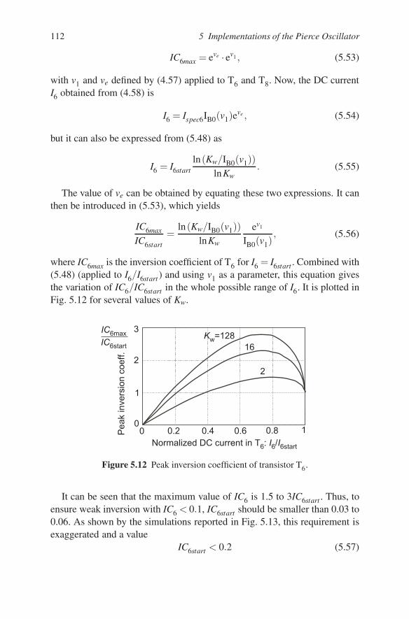
112 5 Implementations of the Pierce Oscillator
IC6max = eve · ev1 , (5.53)
with v1 and ve defined by (4.57) applied to T6 and T8. Now, the DC currentI6 obtained from (4.58) is
I6 = Ispec6IB0(v1)eve , (5.54)
but it can also be expressed from (5.48) as
I6 = I6start
ln(Kw/IB0(v1))lnKw
. (5.55)
The value of ve can be obtained by equating these two expressions. It canthen be introduced in (5.53), which yields
IC6max
IC6start=
ln(Kw/IB0(v1))lnKw
ev1
IB0(v1), (5.56)
where IC6max is the inversion coefficient of T6 for I6 = I6start . Combined with(5.48) (applied to I6/I6start ) and using v1 as a parameter, this equation givesthe variation of IC6/IC6start in the whole possible range of I6. It is plotted inFig. 5.12 for several values of Kw.
+?#,
+
& & &+ &,
);9 >+=+%+
3 &
+"
+
Figure 5.12 Peak inversion coefficient of transistor T6.
It can be seen that the maximum value of IC6 is 1.5 to 3IC6start . Thus, toensure weak inversion with IC6 < 0.1, IC6start should be smaller than 0.03 to0.06. As shown by the simulations reported in Fig. 5.13, this requirement isexaggerated and a value
IC6start < 0.2 (5.57)

Low-Power Crystal and MEMS Oscillators 113
is sufficient to remain very close to the theoretical result for weak inversion(shown in dotted line).
But if Ispec6 is reduced further, the voltage scale is expanded at high cur-rent because of strong inversion, but unchanged at low current. As a con-sequence, the slope svi increases at intermediate current levels, and finallybecomes negative. The overall loop will then be unstable.
The inversion coefficient of T8 is always smaller, since this transistor isKw-times wider as does not receive the AC voltage.
+ ,
&
&
&+
&,
&
+C4E#' '
+?#+
)*"
+
+
#
) +
#& &-&,
Figure 5.13 Effect of strong inversion on the regulator characteristics. The theoret-ical curve for weak inversion is shown in dotted line.
Capacitor C6 is needed in Fig. 5.9(a) to limit the AC drain variation oftransistor T6, thereby keeping it in saturation. For the fundamental compon-ent, the AC amplitude |VD6| at the drain is
|VD6| =1−Gm6(1)R4√1+(ωR4C6)2
V1, (5.58)
with, according to (4.62)
Gm6(1) =I6
|V1|· 2IB1(v1)
IB0(v1)= Gm6 ·
2IB1(v1)
v1IB0(v1). (5.59)
It could in principle be cancelled by choosing Gm6(1)R4 = 1, but the harmoniccomponents would remain. An upper bound of |VD6| including all compon-ents may be estimated by assuming that the drain current is a very large spike

114 5 Implementations of the Pierce Oscillator
of negligible length with respect to the period of oscillation 2π/ω . The drainvoltage would then be a triangular wave of amplitude
|VD6|max∼=
πI6
ωC6. (5.60)
The DC component of gate voltage is obtained by applying (4.58) to tran-sistor T6:
VG06 = VT 0 + nUT lnI6
Ispec6 · IB0(v1). (5.61)
In order to maintain T6 in saturation, C6 should be sufficiently large to ensure
VG06 −|VD6| > 5UT (5.62)
for the largest value I6 = I6start .The values of R4 and R5 should be sufficiently large to limit the loss con-
ductance G1 of the oscillator.The regulator of Fig. 5.9 is a positive feedback loop. At equilibrium, its
open-loop low-frequency gain for constant input voltage |V1| can be calcu-lated to be
GR0(ol) =1
1+ α≤ 1, (5.63)
with
α VR6
nUT=
I0
I0startlnKw, (5.64)
where VR6 is the voltage across resistor R6. This gain is always smaller thanunity, but it approaches unity if the bias current becomes much smaller thanthe start-up current.
If the output noise current spectral density (noise content of current I0) inopen-loop is Si2n0(ol), when the loop is closed it becomes
Si2n0=
(1
1−G0
)2
Si2n0(ol) =(
1+1α
)2
Si2n0(ol), (5.65)
showing that the noise content of the output current I0 increases with I0max/I0.This noise may be reduced by an RC filter before it reaches the gate of T2,but care must be taken to maintain the stability of the overall amplitude reg-ulating loop discussed in Section 5.2.3.
For a frequency Ω much lower than the frequency Ωci of each of theN poles inside the regulator loop, the phase of the open-loop gain can beapproximated by

Low-Power Crystal and MEMS Oscillators 115
ΦR(ol) = −N
∑1
ΩΩci
. (5.66)
Hence, the closed-loop gain GR (for constant |V1|) is given by
1GR
=1
GR0(ol)(1+ jΦR(ol))−1 =
α − jΦR(ol)
1+ ΦR(ol). (5.67)
For ΦR(ol) 1, it becomes
GR =1+ jΦR
α, (5.68)
withΦR = ΦR(ol)(1+ 1/α). (5.69)
Thus, reducing the value of α also results in an increase of the phase shiftin the regulator, which may endanger the stability of the regulation loop.According to (5.64), the ratio I0start/I0 must therefore be limited.
If R4 is a perfectly linear resistor, the DC voltage component at the drainof T6 is equal to that at its gate. Thus, the resistor R5 of the low-pass filtercan be connected to the drain instead of the gate, as illustrated in dottedline in the figure. This variant offers the advantage of reducing the load onthe oscillator. Furthermore, it improves the attenuation of the residual ACcomponent that reaches the gate of T8.
A very large value of ratio Kw is required to reach an amplitude largerthan 4UT , as can be seen in Fig. 5.10(a). Instead, the regulated amplitude canbe increased by attenuating the input voltage of the regulator. This can bedone by adding a capacitor C7 shown in dotted line in Fig. 5.9(a). A part ofC7 can be the gate capacitance of transistor T6. It can be shown that, sincethis transistor is in weak inversion, its gate capacitor is the oxide capacitormultiplied by (n−1)/n < 1.
5.2.3 Amplitude Regulating Loop
The amplitude regulating loop is realized by combining the oscillator ofFig. 5.1 with the regulator of Fig. 5.9(a). The input of the regulator is con-nected to the gate of T1, since it is the gate voltage amplitude that needs tobe regulated.
As illustrated in Fig. 5.14, a stable amplitude is reached at the intersectionS of the |V1|(I0) function of the oscillator with the I0(|V1|) function of the

116 5 Implementations of the Pierce Oscillator
*
<
55
4
**?3
" B
$
DI
) J
Figure 5.14 Amplitude regulating loop; a stable amplitude is reached at point Sif the regulator has the monotonic descending transfer function obtained in weakinversion. If it leaves weak inversion, monotonicity is lost and a relaxation cyclemay occur.
regulator. But this is true only if the current delivered by the regulator isdescending monotonically when the amplitude increases, as obtained whenthe transistor T6 is maintained in weak inversion by observing the condition(5.57).
This monotonicity is lost if the transistor leaves weak inversion during thepeaks of AC current. If the intersection with the |V1|(I0) function of the os-cillator occurs in a region of positive slope (point U), the loop is no longerstable. Instead, a relaxation cycle takes place, as shown in interrupted linein the figure. At start-up, the amplitude |V1| increases and the current I0decreases down to point M where the slope becomes positive. The currentjumps abruptly to a very low value (point O) where the amplitude starts de-creasing, until point P is reached. The current then jumps to a high value atpoint N and the cycle is repeated.
A negative slope of the regulator is thus a necessary condition for a stableloop, but this condition is not sufficient. Indeed, the loop must also satisfythe Nyquist criterion of stability.
Neglecting all other poles than the dominant pole Ωciv of the oscillatoramplitude, the gain of the open loop is obtained by combining (5.25), (5.26)and (5.52):
Gol δV1
δ ID0· δ I0
δ |V1|=
KivGvi
s+ Kiv/Riv, (5.70)

Low-Power Crystal and MEMS Oscillators 117
variable Example 1 Example 2 unit referenceC7/C4 0 1 choiceKw 16 8 choiceI0/Istart 0.12 0.21 Fig. 5.10aI0start 1.17 ·10−6 7.24 ·10−3 A from I0Ki 10 100 choiceI6start 0.117 ·10−6 72.4 ·10−6 A from I0startR6 0.617 ·106 74.7 ·103 V/A (5.45)Ispec6 584 ·10−9 362 ·10−6 A (5.57)W6/L6 1.17 724L6 = L8 2 ·10−6 0.5 ·10−6 m choiceW6 2.34 ·10−6 362 ·10−6 mW8 = KwW6 37.4 ·10−6 2.89 ·10−3 mv1C4/(C4 +C7) 4 3−svi 0.31 0.39 (5.51)−Gvi 10.8 ·10−6 83.4 ·10−3 A/V (5.52)Ω1 23 96.5 ·103 1/s (5.71)Ω0/Ω1 1400 706
Table 5.2 Examples of practical implementations of the amplitude regulator.
where Kiv and Riv and Gvi are given by (5.28), (5.27) and (5.52) respectively.For very low frequencies including DC, it has the absolute value RivGvi thatshould be sufficiently higher than unity to obtain a good regulation. But forfrequencies higher than Ωciv = Kiv/Riv, it behaves as an integrator with aunity gain frequency (or gain-bandwidth product) simply given by
Ω1 = Kiv|Gvi|. (5.71)
There are several other poles in the loop. Indeed, we have seen that thedynamic behavior of the oscillator bias has a resonant frequency with twopoles at Ω0. Moreover, the basic regulator of Fig. 5.9(a) may introduce threemore poles. For loop stability, each of these poles should be at frequencymuch higher than Ω1. If this condition is verified, the phase margin at Ω1can be approximated by using (5.69) and (5.66):
∆Φ =Π2−2
Ω1
Ω0− (1+ 1/α)
N
∑i=1
Ω1
Ωci, (5.72)
where N is the number of poles in the regulator and Ωci the frequency of polei.
Examples of implementation of regulators adapted to the two examples ofoscillators described in the previous sections (Tables 4.1, 4.2, 4.3 and 5.1)are given in Table 5.2.

118 5 Implementations of the Pierce Oscillator
To avoid a too large value of Kw in Example 2, the input voltage of theregulator is divided by two by introducing C7 = C4. The regulator is thendesigned for v1 = 3 instead of 6.
In this example, in spite of a large current ratio Ki, a very large width oftransistors T6 and T8 is needed to maintain them in weak inversion.
For both examples, the unity gain frequency Ω1 is, as it should, muchlower than the resonant frequency Ω0 of the biasing circuit. The loop willbe stable if the additional poles due to the regulator itself are also at a muchhigher frequency. Their number and their values depend on the specific im-plementation of the regulator. Several possibilities will be discussed in thefollowing sections.
5.2.4 Simplified Regulator Using Linear Resistors
If R4 is a linear resistor, the DC component VD0 of drain voltage remainsequal to VG0 at the gate. If C6 is sufficiently large, it will limit the amplitudeof drain voltage |VD6| evaluated by (5.58) to a very low value, so that thelow-pass filter R5C5 can be removed, as shown in Fig. 5.15. For a correct
Figure 5.15 Simplified form of the regulator; the low-pass filter R5C5 is suppressedand T8 is driven directly by the DC component of drain voltage VD06 that followsVG06.
operation of the regulator, the residual AC amplitude |VD6| should be smallerthan about 0.3nUT . If the required value of C6 is to large, it might be betterto keep the additional low-pass filter R5C5.
Another simplified version of the regulator is depicted in Fig. 5.16(a).Here, the low-pass filter R5C5 is maintained, but the drain of T6 is directlyconnected to the gate. This transistor is therefore a nonlinear load for the

Low-Power Crystal and MEMS Oscillators 119
>+
'
+
$',
<
+$, ,
'
>,
>.
>->
-
+ ,
&
&
&+
&,
&
)"#55
) >
+
+
Figure 5.16 (a) Simplified form of the regulator; the drain of T6 is directly connec-ted to the gate. (b) The equivalent conductance loading the oscillator is smaller thanthe small-signal transconductance Gm6.
oscillator, which should be made negligible. The contribution to G1 is thetransconductance for the fundamental component Gm6(1) given by (5.59) andplotted in Fig. 5.16(b).
Thanks to the DC shift, it is always smaller than the small-signal conduct-ance Gm6 for ID6 = I6. To avoid a too large loss conductance G1, the branchcurrent I6 should be much smaller than the bias current I0 of the oscillator.
The most compact solution is obtained by merging the regulator with theoscillator as illustrated in Fig. 5.17 [21]. Transistors T6 and T7 of the reg-
<
>
>
'+
,
'
>,
>.
Figure 5.17 Compact regulating loop by merging the oscillator with the regulator.
ulator are merged with T1 and T2 of the oscillator, so that T1 and T8 havethe same DC gate voltage. Since transistor T6 must be in weak inversion,

120 5 Implementations of the Pierce Oscillator
this solution is only possible if the oscillator is designed with T2 in weakinversion, with Ispec1 > 5I0start according to (5.57).
5.2.5 Elimination of Resistors
A possible implementation of the regulator without any resistor is depictedin Fig. 5.18.
>+
$',
<
+$,,
+
>,
>.
>->
,
> >
>
>
>
>'
'
>'
Figure 5.18 Possible implementation of the amplitude regulator without resistors.Resistor R4 of Fig. 5.15 is replaced by transistor T12; this modifies the characteristicsof the regulator. Resistor R6 is replaced by transistor T10.
The role of resistor R6 of the original circuit (Fig. 5.9) is to define thevalue of start-up current. It is here replaced by transistor T10 operating instrong inversion with VD VDsat (or IF − IR IF ). The corresponding res-istance is the inverse of the source transconductance of T10 given by (3.50).If transistors T10 and T11 are identical, the equivalent resistance is then
R6 =UT√
IF10Ispec10=
UT√I11Ispec10
. (5.73)
The bias current I11 must be provided by some external current reference.This could be avoided by suppressing T11 and connecting the gate of T10 tosome bias voltage Vb. From (3.50), the equivalent resistance would then be
R6 =1
β10(Vb −VT0). (5.74)
A simple possibility is to use the supply voltage VB as bias voltage Vb, withthe risk of perturbing the oscillator by the noise content of VB.
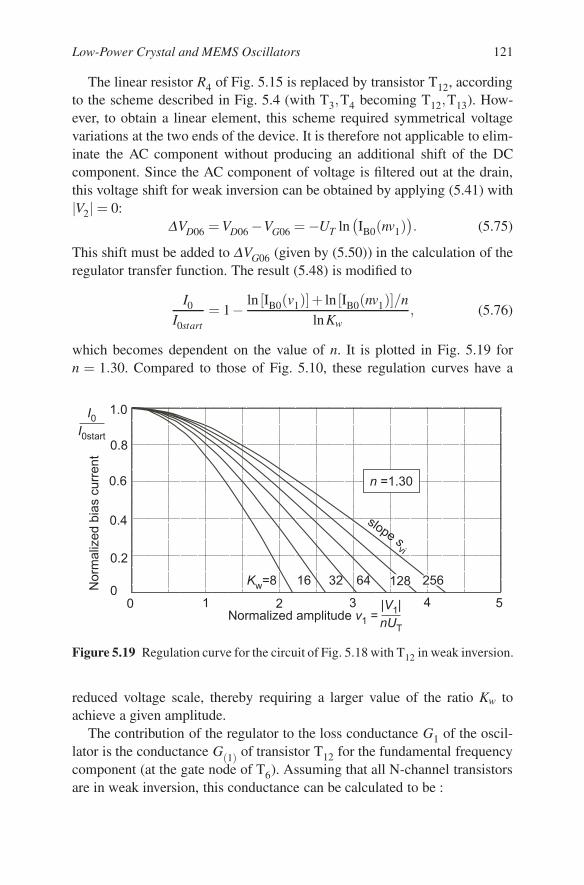
Low-Power Crystal and MEMS Oscillators 121
The linear resistor R4 of Fig. 5.15 is replaced by transistor T12, accordingto the scheme described in Fig. 5.4 (with T3,T4 becoming T12,T13). How-ever, to obtain a linear element, this scheme required symmetrical voltagevariations at the two ends of the device. It is therefore not applicable to elim-inate the AC component without producing an additional shift of the DCcomponent. Since the AC component of voltage is filtered out at the drain,this voltage shift for weak inversion can be obtained by applying (5.41) with|V2| = 0:
∆VD06 = VD06 −VG06 = −UT ln(IB0(nv1)
). (5.75)
This shift must be added to ∆VG06 (given by (5.50)) in the calculation of theregulator transfer function. The result (5.48) is modified to
I0
I0start= 1− ln [IB0(v1)]+ ln [IB0(nv1)]/n
lnKw, (5.76)
which becomes dependent on the value of n. It is plotted in Fig. 5.19 forn = 1.30. Compared to those of Fig. 5.10, these regulation curves have a
&
&
&+
&,
&
'
+?#, + + , '+
)#&
)"#55
) >
)
Figure 5.19 Regulation curve for the circuit of Fig. 5.18 with T12 in weak inversion.
reduced voltage scale, thereby requiring a larger value of the ratio Kw toachieve a given amplitude.
The contribution of the regulator to the loss conductance G1 of the oscil-lator is the conductance G(1) of transistor T12 for the fundamental frequencycomponent (at the gate node of T6). Assuming that all N-channel transistorsare in weak inversion, this conductance can be calculated to be :

122 5 Implementations of the Pierce Oscillator
G(1) = G0 ·2IB1(nv1)
nv1. (5.77)
This result is identical to (5.37) plotted in Fig. 5.6, but the small signal valueG0 is
G0 = e(VG14−VG06)/UTI8
KrUT(5.78)
with Kr = β13/β12. The voltage difference (VG14 −VG06) depends on the rel-ative size of transistors T6 and T14 and on the shift of DC gate voltage of T6given by (5.50):
VG14 −VG06 = nUT · ln[
β6
β14IB0(v1)
], (5.79)
thus (5.78) becomes
G0 =[
β6
β14IB0(v1)
]n I8
KrUT, (5.80)
which is can be made independent of n by choosing β14/β6 = IB0(v1).To improve the amount of filtering, the low-pass filter R5C5 of Fig. 5.9(a)
can be implemented by means of an additional transistor T15 (shown in dot-ted line in Fig. 5.18) with the same gate voltage as T12. This transistor doesnot produce any voltage shift since it only receives the very small residualAC voltage, but it should have a smaller value of specific current to com-pensate for the additional voltage shift given by (5.75). To obtain the samesmall signal conductance G0 as T12:
β15 = β12/IB0(nv1). (5.81)
Now, even if T12 and T13 are in strong inversion, with inversion coef-ficients IC12 = IC13 much larger that unity, T12 cannot behave as a linearresistor, since there is no AC voltage at the drain of T6. The voltage shift canbe calculated to be
∆VD06 = VD06 −VG06 = 2UT
√IC13
[1−
√1− |V1|2
8U2T IC13
], (5.82)
which is only valid if the peaks of V1 do not saturate T12, i.e. for
|V1| < 2UT
√IC13. (5.83)
This shift can be made negligible with respect to ∆VG06 expressed by (5.50)by choosing a large value of inversion coefficient IC13. The basic regulationcurves of Fig. 5.10(a) will then remain valid.
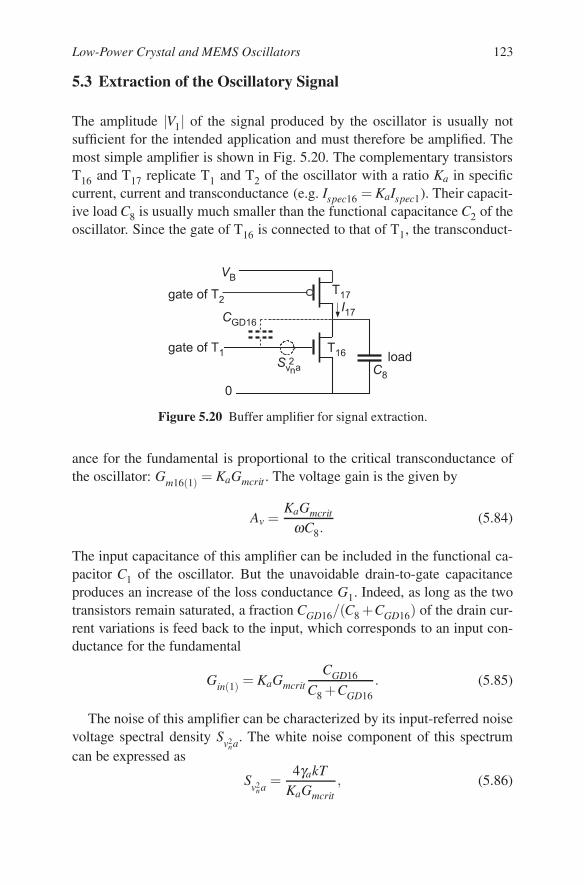
Low-Power Crystal and MEMS Oscillators 123
5.3 Extraction of the Oscillatory Signal
The amplitude |V1| of the signal produced by the oscillator is usually notsufficient for the intended application and must therefore be amplified. Themost simple amplifier is shown in Fig. 5.20. The complementary transistorsT16 and T17 replicate T1 and T2 of the oscillator with a ratio Ka in specificcurrent, current and transconductance (e.g. Ispec16 = KaIspec1). Their capacit-ive load C8 is usually much smaller than the functional capacitance C2 of theoscillator. Since the gate of T16 is connected to that of T1, the transconduct-
>+
-
,
>-
:;+
<
*>
*>
Figure 5.20 Buffer amplifier for signal extraction.
ance for the fundamental is proportional to the critical transconductance ofthe oscillator: Gm16(1) = KaGmcrit . The voltage gain is the given by
Av =KaGmcrit
ωC8.(5.84)
The input capacitance of this amplifier can be included in the functional ca-pacitor C1 of the oscillator. But the unavoidable drain-to-gate capacitanceproduces an increase of the loss conductance G1. Indeed, as long as the twotransistors remain saturated, a fraction CGD16/(C8 +CGD16) of the drain cur-rent variations is feed back to the input, which corresponds to an input con-ductance for the fundamental
Gin(1) = KaGmcritCGD16
C8 +CGD16. (5.85)
The noise of this amplifier can be characterized by its input-referred noisevoltage spectral density Sv2
na. The white noise component of this spectrumcan be expressed as
Sv2na =
4γakTKaGmcrit
, (5.86)

124 5 Implementations of the Pierce Oscillator
where γa is the noise excess factor of the amplifier. This factor is always lar-ger than 1/2, but it may be much larger than unity if T16 is in strong inversionwith an inversion coefficient much larger than that of T17.
This voltage noise results in a component of phase noise, with a spectrumgiven by given by
Sφ 2n a = Sv2
na/|V2
1 |. (5.87)
This noise is added to the phase noise of the oscillator (given by (3.29) or(3.30)) and dominates at frequencies distant from the frequency of oscilla-tion.
5.4 CMOS-Inverter Oscillator
5.4.1 Direct Implementation
One of the earliest implementations of a CMOS oscillator is illustrated byFig. 5.21. It is a simple CMOS inverter biased in active mode by a resistor
<
Figure 5.21 Direct implementation of a CMOS inverter as an oscillator.
R, to which the two functional capacitors of the Pierce circuit are added.It is still a grounded-source configuration, since both sources are groundedwith respect to AC signals. The transconductances of the two transistors areadded, but they are produced by the same current I0. If the transistors aredesigned to have the same specific current, the combined transconductanceis doubled. According to (3.55), the critical current is thus reduced by a factor2 for any given value of inversion coefficient IC0.
However, this simple circuit suffers from two major drawbacks.

Low-Power Crystal and MEMS Oscillators 125
First, the current drawn from the supply voltage is not constant and itsaverage value I0 depends on the supply voltage and on the threshold voltageof the two transistors. This dependency increases when the inversion factoris decreased and is maximum in weak inversion.
The second drawback is that, at low values of the inversion coefficient,the nonlinearity of the transfer function of the inverter results in an increaseof the transconductance for the fundamental frequency Gm(1) with the amp-litude of oscillation. Thus, as soon as the critical transconductance is reached(for a critical value of VB), the amplitude increases abruptly, until it is lim-ited by the loss conductance of the transistors leaving saturation in the peaksof oscillation. The corresponding variation of Zc(1)(|Ic)| simulated in an ex-ample is shown in Fig. 5.22. The simulated circuit is depicted in part (a) of
<#&,8
<#&8
&',&'
+&'
&'
,&'
&'
!
%#3F
&+
&
<#&8
<#&+8
<#&8
5 5Cµ4E#&
5 5C8%4E
&#/
#/ #/
DΩ
<
#&µ4
#&'µ4
Figure 5.22 Simulation of the circuit impedance for the fundamental frequencyZc(1) of a CMOS-inverter oscillator.
the figure. The two complementary transistors have approximately identicalspecific currents and the loss due to the biasing resistor is practically negli-gible.
Part (b) of the figure shows the loci of Zc(1)(|Ic|) calculated from simula-tions with several values of supply voltage VB. As long as the amplitude |Ic|of the sinusoidal current injected in the circuit is smaller than 100nA, the cir-
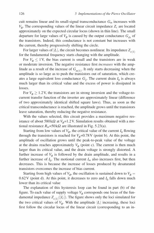
126 5 Implementations of the Pierce Oscillator
cuit remains linear and its small-signal transconductance Gm increases withVB. The corresponding values of the linear circuit impedance Zc are locatedapproximately on the expected circular locus (shown in thin line). The smalldeparture for large values of VB is caused by the output conductance Gds ofthe transistors. Indeed, this conductance is not constant but increases withthe current, thereby progressively shifting the circle.
For larger values of |Ic|, the circuit becomes nonlinear. Its impedance Zc(1)for the fundamental frequency starts changing with the amplitude.
For VB ≤ 1V, the bias current is small and the transistors are in weakor moderate inversion. The negative resistance first increases with the amp-litude as a result of the increase of Gm(1). It only starts decreasing when theamplitude is so large as to push the transistors out of saturation, which cre-ates a large equivalent loss conductance G2. The current drain I0 is alwaysmuch larger than its critical value and the excess of power is dissipated inlosses.
For VB ≥ 1.2V, the transistors are in strong inversion and the voltage-to-current transfer function of the inverter are approximately linear (differenceof two approximately identical shifted square laws). Thus, as soon as thecritical transconductance is reached, the amplitude grows until the transistorsleave saturation, thereby reducing the negative resistance.
With the values selected, this circuit provides a maximum negative res-istance of about 580kΩ at VB=1.2V. Simulation results obtained with a mo-tional resistance Rm=50kΩ are illustrated in Fig. 5.23(a).
Starting from low values of VB, the critical value of the current I0 flowingthrough the transistors is reached for VB=0.78V (point b). At this point, theamplitude of oscillation grows until the peak-to-peak value of the voltageat the drains reaches approximately VB (point c). The current is then muchlarger than its critical value, and the drain voltage is strongly distorted. Afurther increase of VB is followed by the drain amplitude, and results in afurther increase of I0. The motional current Im also increases first, but thendecreases. This is because the increase of losses produced by desaturatedtransistors overcomes the increase of bias current.
Starting from high values of VB, the oscillation is sustained down to VB =0.62V (point d). At this point, it decreases to zero and I0 falls down muchlower than its critical value
The explanation of this hysteresis loop can be found in part (b) of thefigure. To each value of supply voltage VB corresponds one locus of the fun-damental impedance Zc(1)(|Ic|). The figure shows only the loci simulated forthe two critical values of VB. With the amplitude |Ic| increasing, these locifirst follow the circular locus of the linear circuit (corresponding to an in-

Low-Power Crystal and MEMS Oscillators 127
& &+ &, & & &
&'
&
&'
&
&'
B*<C8E
55Cµ4E
Cµ4E
<
#'3Ω
3
3
C
8E
<#&-,8&'&'&'&'
&'&'
<#&+8
#'&
C8%4E
Figure 5.23 Simulation of the CMOS inverter-oscillator of Fig. 5.22(a) withRm =50 kΩ ; (a) variation of motional current, current drain and peak-to-peak drainamplitude; (b) partial Zc(1) complex plane explaining the hysteresis loop.
crease of the negative resistance |Rn|). This is because Gm(1) increases withthe amplitude, as explained above. When the losses at the drain becomestoo important, the loci loop back and the negative resistance decreases asnormally.
The locus of the motional impedance −Zm(p) for Rm=50kΩ is repres-ented in dotted line in the same figure. As explained in Chapter 3, stableoscillation can be reached for Zc(1) = Zm.
Starting from low values of VB, the first solution is found at point b (originof the Zc(1) locus for VB = 0.78V). But this solution is unstable since theamplitude stability criterion (1.3) is not met. At this value of VB, the amp-litude first increases and then decreases until the stable point c is reached.Larger values of VB correspond to lower positions of this stable solution.
When VB is reduced below 0.78V, the stable solution will move on inter-mediate loci, until point d is reached for VB=0.62V. But this point is meta-stable since for any small change of amplitude the negative resistance be-comes smaller than Rm. At this value of VB, the amplitude decreases untilpoint a is reached.
This hysteresis loop can disappear if the transistors are both in stronginversion at the critical value of VB. But this requires a higher value of VBand the critical current is increased, thus the advantage of minimizing thecurrent is lost. It is very difficult in practice to avoid dissipating much morepower than the minimum needed for a given amplitude of oscillation.

128 5 Implementations of the Pierce Oscillator
The current (and thus the excess of negative resistance) is strongly de-pendent on the supply voltage and on the gate threshold voltage of the tran-sistors. Since the amplitude limitation is achieved by increasing the losses,the amount of frequency pulling depends also strongly on these voltages andthus on the temperature. Furthermore, because of this strong possible over-drive, this circuit is prone to parasitic oscillation on unwanted modes of theresonator.
Its only advantages are a possible rail-to-rail output (peak-to-peak drainvoltage close to VB) and a large power efficiency
η =Pm
VBI0. (5.88)
The mechanical power Pm and the efficiency η calculated from the simula-tion of the circuit of Fig. 5.22 are plotted in Fig. 5.24. The power efficiency
& &+ &, & & &
,
+
'
+
-
-
η
B*<C8E
D ( ?
? B
η -CKE
Figure 5.24 Mechanical power and power efficiency of the CMOS inverter-oscillator of Fig. 5.22(a) with Rm =50 kΩ .
reaches a maximum close to 50% at the minimum value of VB but decreasesfor higher values with the increase of losses.
Compared to the current-biased Pierce oscillator, the high value of Pm (andthus of Em for a given value of Q) might be an advantage to reduce the phasenoise, according to (3.30). However, the noise excess factor γ is increased bya higher current due to losses, which compensates this higher energy of os-cillation. Moreover, for high frequency resonators, Pm might largely exceedthe acceptable value (it was close to the limit in Example 2 of Tables 4.1 to4.3).
In spite of its apparent simplicity the direct implementation of a CMOSinverter-oscillator illustrated in Fig. 5.21 is not recommended because of itsmany pitfalls.

Low-Power Crystal and MEMS Oscillators 129
5.4.2 Current-controlled CMOS-inverter oscillator
The best way of exploiting the increased transconductance provided bya complementary inverter is to impose its bias current as illustrated byFig. 5.25 [22].
<
>
Figure 5.25 CMOS-inverter oscillator biased by current I0. The coupling capacitorCc is necessary to activate the P-channel transistor.
As for the basic grounded source circuit of Fig. 5.1 and all its variantsand extensions, the bias current I0 is imposed by transistor T2. A couplingcapacitor Cc must be added to ensure the activity of the P-channel part of theinverter. Its impedance must be much lower than the source transconduct-ance of the transistor. Assuming that the two complementary transistors haveabout the same transconductance (otherwise the complementary scheme isuseless):
ωCc nGmcrit/2 (5.89)
For the Example 1 of Section 4.5.2, this gives Cc 4.9pF, thus a largecapacitance of at least 50pF is needed.
The large signal behavior of this complementary circuit is exactly thesame as that of the basic circuit. When the amplitude grows, the DC compon-ent VG0 of the N-channel transistors decreases by ∆VG0 according to Fig. 4.18to keep I0 constant. For the P-channel transistor, the current is kept constantby a decrease ∆V0 of the voltage V0 at its source. According to (3.40), thesaturated drain current is controlled by VG − nVS. Hence, for symmetricaltransistors (Ispecp = Ispecn):
∆V0 = 2∆VG0/n. (5.90)

130 5 Implementations of the Pierce Oscillator
To minimize losses, the two transistors should remain saturated in thepeaks of drain amplitude:
VDS0n + |V2| < VDSsatn and VDS0p + |V2| < VDSsat p, (5.91)
where VDS0n and VDS0p are the DC component of the voltage across the tran-sistors, and |V2| is, as before, the amplitude of oscillation at the drain.
Considering the case of weak inversion, (4.58), VDS0n is obtained directlyfrom (4.68):
VDS0n = VG0n = VT 0n −nUT ln
[Ispec
I0critmin·
2IB1(v1)
v1
](5.92)
The same DC current I0 flows through the two complementary transistors.It is given by (4.58) with
ve = ven =VGon −VT0n
nnUT(5.93)
for the N-channel transistor and
ve = vep =VGop −VT0p −nVSp
npUT(5.94)
for the P-channel device (with the definitions of Fig. 3.10 for voltages). Ifthe transistors are symmetrical (Ispecp = Ispecn and np = nn), equating the twoexpressions of I0 yields
VSp = (VG0p −VT0p −VG0n +VT0n)/n, (5.95)
where VT 0n and VT 0p are the values of threshold VT 0 for the two types oftransistors. Now VG0p = VB −VG0n, thus
VDS0p = VG0p −VSp = VB
(1− 1
n
)+VG0n
(2n−1
)+
VT 0p −VT0n
n, (5.96)
or, by introducing (5.92)
VDS0p =VT 0p
n+
n−1n
(VB −VT0n)− (2−n)UT ln
[Ispec
I0critmin·
2IB1(v1)
v1
].
(5.97)The drain amplitude |V2| must then be limited to fulfill the two condi-
tions of (5.91) with VDSsatn = VDSsat p∼= 5UT . If needed, the DC voltage VDS0n

Low-Power Crystal and MEMS Oscillators 131
<
>
∆
∆
Figure 5.26 CMOS-inverter oscillator modified to allow an increase of drain amp-litude.
across the N-channel transistor can be increased by one of the schemes dis-cussed in Section 5.1.6.
If the DC voltages across both transistors must be increased, the solutiondepicted in Fig. 5.26 can be implemented. Two separate resistors Rn and Rp
are used to bias the gates of the two transistors, and a small current Ib is flownthrough them. The voltage drops ∆Vn and ∆Vp across them are equivalent toan increase of VT n and VT p in equations (5.92) and (5.96). The gate of theP-channel transistor is coupled by means of capacitor Cp.
If transistors must be used to implement resistors, the floating resistor Rp
is hard to realize. It is then better to bias the gate of the P-channel transistorfrom a separate voltage source of adequate value.
As shown by (5.96), VDS0p increases with VB. This would not be the caseif the P-channel transistor were put in a separate well connected to its source(as indicated in dotted line in Fig. 5.25). The DC voltage across the transistorwould then be symmetrical to that of the N-channel device:
VDS0p = VG0p = VT 0p −nUT ln
[Ispec
I0critmin·
2IB1(v1)
v1
], (5.98)
which is always smaller than the value given by (5.96). The advantage wouldbe a reduction of the minimum value of supply voltage VB.

132 5 Implementations of the Pierce Oscillator
5.5 Grounded-Drain Oscillator
5.5.1 Basic Implementation
The basic grounded-drain version of the Pierce oscillator is shown in Fig. 5.27.To avoid modulation by the source, the active transistor T1 is put in a sep-
;
<
$#
>
>
Figure 5.27 Basic grounded-drain version of the 3-point Pierce oscillator.
arate well connected to its source. In this N-channel implementation, thedrain of T1 is connected to the positive rail of the power supply (which isthe ground of the AC signal), and a bias current I0 is delivered by a currentsource T2 (also N-channel). As in the grounded-source version, T1 is biasedin saturation by means of resistor R3.
All the results obtained in Chapter 4 for the Pierce oscillator are applicableto this circuit. But there are some notable differences with respect to thegrounded-source implementation of Section 5.1.
One side of the resonator is grounded. Therefore, only one additional pinis needed, hence its appellation “single pin oscillator” [23]. But this advant-age also turns out to be a drawback, since C3 now includes parasitic capacit-ors to ground (connecting pad, package feedthrough, external connections).Even if these are minimized, it includes C10 or C20 of the resonator itself.As a result, C3 becomes much larger than its minimum value C12 due to theresonator. The radius of the circular locus of Fig. 4.6 and the margin factorKm defined by (4.17) are thus drastically reduced, with the various negativeconsequences discussed in Chapter 4.
One potential advantage of this implementation is that the voltage V3across the resonator can be used as the output signal. As expressed by (4.37)this voltage is larger than V1. However, this will further increase the over-

Low-Power Crystal and MEMS Oscillators 133
all value of C3. It might also increase the loss conductance G3, which has astrong effect on the critical transconductance, according to (4.45).
Another negative point is the fact that the relatively large capacitanceto ground of the separate well is now part of C2. Since this capacitance isvoltage dependent, the frequency stability is degraded.
As for the grounded-source realization, even with a large value of supplyvoltage, the maximum amplitude is limited by the desaturation of the activetransistor in the peak of oscillation. This limit can be pushed by flowing somecurrent through the bias resistor R3, thereby lowering the DC voltages at thegate and at the source and substrate node.
The resistor can be implemented by means of a P-channel transistor T3biased in the linear region of strong inversion. Then, according to (3.50):
R3 =1
Gms3=
UT√IF3Ispec3
. (5.99)
The circuit of Fig. 5.27 assumes that a the N-channel active transistor canbe put in a separate P-type well. If only N-type wells are available, P-channeldevices must be used.
The amplitude of oscillation can be controlled by the regulator discussedin Section 5.2 (or by its P-channel version). This circuit can be capacitivelycoupled to the gate of T1 to control |V3|, or to its drain to control |V2|. Itdelivers the bias current I0.
5.5.2 Single-Substrate Implementation
It might be tempting to avoid a separate well for the active transistor T1 andto realize the circuit as shown in Fig. 5.28. This was the only possibility forthe first implementation of this oscillator in a P-MOS process [24]. The com-mon substrate of the N-channel devices is now the negative rail of the powersupply (reference 0). The source voltage VS and drain voltage VG are bothchanging with the oscillatory signal, whereas the drain voltage is constantand equal to VB.
The general expression of the circuit impedance Zc is now
Zc =Z1Z3 + Z2Z3 + nGmZ1Z2Z3
Z1 + Z2 + Z3 + GmZ2[nZ1 +(n−1)Z3], (5.100)
where each impedance Zi is defined by (4.1). It would be reduced to (4.2)(impedance of the basic circuit) for n = 1. The circuit impedance is still a

134 5 Implementations of the Pierce Oscillator
:
;
<
$
>
>
Figure 5.28 Grounded-drain 3-point Pierce oscillator without separate well.
bilinear function of the gate transconductance Gm, hence the locus of Zc(Gm)is still a circle.
For the lossless circuit (Zi = 1/ jωCi), this circle is centered on the ima-ginary axis, as illustrated in Fig. 5.29.
% )
&
&
&)
!
ω
ω))
ω
55"
@#
#
ω))
#&
Figure 5.29 Loci of Zc(Gm): a: Single-substrate with C1 = C2; b: separate wellwith C1 = C2 (optimum ratio); c: single-substrate with C2/C1 = 2n− 1 (optimumratio). All three loci have the same value of Cs +C3, thus same frequency pullingfor Rm |Rn0|max. The radius of the loci for the single-substrate is dramaticallyreduced.
Compared to the basic implementation of Fig. 5.27 (corresponding to n =1), the upper point of the circle (Gm = 0) is not changed, but the lower point(Gm = ∞) is much higher, due to the term C1(n− 1)/n added to C3. Theradius of the circle is therefore drastically reduced. The maximum value ofnegative resistance (radius of the circle) is reduced to

Low-Power Crystal and MEMS Oscillators 135
|Rn0|max =n− (n−1)C1/Cs
2ωC3(1+C3/Cs)(n+(n−1)C1/C3), (5.101)
where Cs is the series combination of C1 and C2.For Rm |Rn0|max (which is much more difficult to satisfy), the critical
transconductance for the lossless case is
Gmcrit0∼=
ω2Rm(C1C2 +C2C3 +C3C1)2
C1[C2 − (n−1)C1], (5.102)
or, by combination with (4.21) (which is not modified):
Gmcrit0∼=
ωCm
Qp2c· (C1 +C2)
2
4C1[C2 − (n−1)C1], (5.103)
which reduces to (4.26) for n = 1. The optimum is no longer for C1 =C2, butfor
C2 = (2n−1)C1 giving Gmcrit0∼= n
ωCm
Qp2c. (5.104)
Thus, even with the optimum capacitance ratio, the critical transconductancefor a given value of frequency pulling is increased by factor n. As shown inFig. 5.28 (curve c), the radius of the locus is slightly larger than for C1 = C2(curve a), but still much smaller than for the optimum implementation witha separate well (curve b).
In summary, the implementation of the grounded-drain Pierce oscillator ina single substrate (with no separate well) strongly reduces the radius of thecircular locus, thereby reducing the margin factor Km defined by (4.17). Theminimum critical transconductance is increased and is obtained with C1 <C2(and thus |V1| > |V2| according to (4.38)). In view of these many drawbacks,this solution should be avoided.

Chapter 6Alternative Architectures
6.1 Introduction
The basic 3-point Pierce oscillator of Fig. 4.1 is the only possible configur-ation of a quartz (or MEMS) oscillator using a single active transistor. Assoon as two or more active transistors are considered, many configurationsbecome possible. Three of them will be discussed in this last Chapter.
Two-transistors symmetrical circuits for parallel and series resonance willbe analyzed in Sections 6.2 and 6.3. An example of more complicated ar-chitecture using an operational transconductance amplifier (OTA) will bypresented more briefly in Section 6.4. These three circuits will be comparedwith the Pierce oscillator in Section 6.5.
6.2 Symmetrical Oscillator for Parallel Resonance
6.2.1 Basic Structure
The standard circuit used for a symmetrical parallel resonance oscillator isillustrated in Fig. 6.1(a). It is based on a known circuit using vacuum tubes(figure 68b, page 82 of [15]). The negative resistance produced by the cross-coupled differential pair is simply
Zc00 = −2/Gm, (6.1)
E. Vittoz, Low-Power Crystal and MEMS Oscillators: The Experience of Watch Developments, 137Integrated Circuits and Systems, DOI 10.1007/978-90-481-9395-0_6, © Springer Science+Business Media B.V. 2010

138 6 Alternative Architectures
<
> >
> >
;
$
$ $
; ;
Figure 6.1 Basic parallel resonance oscillator; (a) standard circuit for a R,L,G res-onator; (b) modified circuit adapted to the absence of a DC path in the resonator(without bias circuitry).
where Gm is the transconductance of each transistor. The critical conditionfor oscillation is thus
Gm = 2G, (6.2)
and oscillation will take place exactly at the resonant frequency of the res-onator, since the circuit admittance is real (except for the effect of parasiticcapacitors).
This circuit produces a voltage stable negative resistance compatible withparallel resonance. It would not provide a stable oscillatory solution with aplain series resonator. One obvious reason is that a DC path is needed acrossthe resonator, otherwise the circuit becomes bistable. But even if bistabilityis avoided by some means, no stable oscillation would be possible, becausethe basic condition (1.2) for phase stability would not be fulfilled. Therefore,if this circuit is associated with a quartz resonator, it must exploit the parallelresonance discussed in Chapter 2. For this parallel resonance, the parallelcapacitance CP is part of the resonator. If necessary, this capacitance may beincreased to a value CD > CP to reduce the amount of frequency pulling.
To eliminate the DC bistable solution, the DC coupling between thesources of the transistors must be replaced by a capacitive coupling CS as il-lustrated in Fig. 6.1(b). The circuit impedance (without parallel capacitance)becomes
Zc0 = − 2Gm
+ jn
ωCS. (6.3)

Low-Power Crystal and MEMS Oscillators 139
Away from the resonant frequencies of the quartz, the drains are simplyconnected by a parallel capacitance CD and a parasitic oscillation may occurat the frequency ωp that cancels the imaginary part of the total admittance:
Im
[1
Zc0(ωp)
]+ ωpCD = 0, (6.4)
which results in
ω2p =
nG2m
4CDCS
(1− nCD
CS
). (6.5)
Thus ifCS < nCD, (6.6)
this frequency does not exist and no parasitic oscillation can occur.
6.2.2 Linear Analysis with the Parallel Resonator
The variation of the parallel impedance Zp of the resonator (i.e with the par-allel capacitance CP across the motional impedance Zm) was discussed inChapter 2, with the locus of Zp(Qp) illustrated in Fig. 2.3. This circularlocus is reproduced in Fig. 6.2, with the figure of merit M replaced by itsvalue for the loaded dipole resonator defined by
ML QCm
CD≤ MD < M0. (6.7)
The circuit impedance Zc0 given by (6.3) (without the parallel capacitanceCD that is now part of the parallel resonator) is a linear function of 2/Gm
with a constant imaginary part. The locus of −ωCDZc0 is plotted in dottedline in Fig. 6.2. It is an horizontal strait line that is below -1 in order to fulfillcondition (6.6). One of its two intersections with ωCDZp(p) corresponds tothe critical condition for oscillation (the other can be shown to be unstable).
As can be seen, the oscillation frequency is always above the parallel res-onance frequency. By introducing the definition (6.7) of ML, the range ofpossible pulling can be expressed as
Cm
2CD≤ pc ≤
Cm
2CD+
12Q
, (6.8)
whereas the range of critical transconductance for the lossless circuit is

140 6 Alternative Architectures
7
7
#
!
$
#
);
$
ω;%
7
#
ω;
ω;
7
ω;% 7%
Figure 6.2 Normalized loci of Zp(p) and −Zc0(Gm). Their intersection defines thecritical condition for oscillation.
2ωCD
ML≤ Gmcrit0 ≤
4ωCD
ML. (6.9)
In normal cases, ML 1 (very large circle) whereas nCD/Cs is not muchlarger than unity. Then Gmcrit0 has the lowest value of this range:
Gmcrit0 =2ωCD
ML=
2ωC2D
QCm= 2ω2C2
DRm. (6.10)
6.2.3 Linear Analysis with the Series Motional Resonator
Although it is basically a parallel resonance oscillator, this circuit can beanalyzed as was done for the previous circuit, by separating the motionalimpedance Zm of the resonator from the overall circuit impedance Zc (thatincludes the parallel capacitance CD). Both approaches are equivalent forthe small-signal linear analysis, but the splitting (Zm,Zc(1)) is needed to con-sider nonlinear effects, as explained in Chapter 3. Indeed, the current flowingthrough Zp is no longer sinusoidal when the voltage across it is distorted.
The impedance of the whole circuit shown in Fig. 6.3(a) in the generalcase with losses is
Zc =ZDZc0
ZD + Zc0=
ZD(2+ nGmZS)2+ nGmZS −GmZD
, (6.11)

Low-Power Crystal and MEMS Oscillators 141
> >$ $
; ;
$
;
∆$
"
*)$
;
%
Figure 6.3 Parallel resonance oscillator with lossy impedances ZS and ZD; (a) fullcircuit without bias; (b) small-signal equivalent circuit.
It corresponds to the small-signal equivalent circuit of Fig. 6.3(b).The values of Zc for the extremes of Gm are
Zc = ZD for Gm = 0 andnZDZS
nZS −ZDfor Gm = ∞. (6.12)
If the two impedances are simply capacitors (lossless circuit), these limitsbecome − j/ωCD and − j/ω(CD −CS/n), and the circular locus of Zc iscentered on the imaginary axis, as illustrated in Fig. 6.4.
The stable locus with CS <CD looks similar to the locus of Zc(Gm) for thePierce lossless oscillator, represented in Fig. 4.6. However, there is a majordifference due to the fact that CD plays the role of C3 +Cs, but can be muchsmaller. The amount of pulling can therefore be larger than for the Piercecircuit, with the advantage of a smaller value of critical transconductance(given by (6.10)), and the drawback of a larger dependency on CD.
As for the Pierce circuit, the locus of −Zm(p) is also represented inFig. 6.4. The critical condition for oscillation is at its intersection A withZc(Gm).
The maximum value of negative resistance is easily obtained by inspec-tion, since it is the radius of the circle:
|Rn0|max =1
2ωCD(nCD/CS −1). (6.13)
It is reached for Gm = Gmopt given by
Gmopt =2ωCD
nCD/CS −1. (6.14)

142 6 Alternative Architectures
ω;$%)
ω;
!
$#);
$@);
$A);
55"
#
#
@ A
*
4
<
Figure 6.4 Loci of Zc(Gm) and −Zm(p) for the circuit of Fig. 6.1(b); the limit casefor nCS = CD and the unstable case for nCS > CD are represented in thinner lines.
The maximum negative resistance increases to infinity for the limit caseCS = nCD. In practice, it is limited by the need to ensure some margin ofsecurity. This margin depends on the worst mismatch expected between CDand CS/n. This mismatch can be large, since the two capacitors do not havethe same structure.
Let us define the maximum relative mismatch
εmax (nCD/CS)max − (nCD/CS)min
(nCD/CS)max +(nCD/CS)min. (6.15)
Since the minimum value of nCD/CS must be larger or equal to unity, itsnominal value must be at least 1/(1− εmax) and its maximum value will be(1+ εmax)/(1− εmax). The maximum value of negative resistance will be inthe range
1− εmax
4ωCD · εmax≤ |Rn0|max ≤ ∞, (6.16)
with CD ≥CP.Now, as was discussed for the Pierce circuit, the motional resistance Rm
should be much smaller than the maximum negative resistance |Rn|max, sothat the point A corresponding to stable oscillation remains located at thetop of the circle. The imaginary part is then −1/ωCD, which introduced in(3.10) gives

Low-Power Crystal and MEMS Oscillators 143
pc =Cm
2CD, (6.17)
the minimum of the range defined by (6.8).By introducing this result in (6.10), the critical transconductance can be
expressed as
Gmcrit0 =ωCm
2Qp2c. (6.18)
An inspection of Fig. 6.3 shows that the amplitudes at the gates and atthe sources are simply related by Vin/∆VS = −Zx/ZS, where Zx is the par-allel combination of Zm and ZD (Zx = Zp if ZD is just the lossless parallelcapacitance CD).
Now, at the critical condition for oscillation, Zx = Zc0. In the lossless case,Zc0 is given by (6.3). Hence, with Gmcrit given by (6.10):
Vin
∆VS= −Zc0
ZS= n+ j
2ωCS
Gmcrit= n+ j
CS
CD· QCm
CD= n+ j
CS
CD·ML. (6.19)
If CD is not too large, the figure of merit ML defined by (6.7) remainsmuch larger than unity. Moreover, CS/CD is close to n. Hence, the voltageratio Vin/∆VS is essentially imaginary and much larger than unity. But thisis no longer true if CD is made much larger than CP to reduce the frequencypulling given by (6.17).
6.2.4 Effect of Losses
The lossy impedance at the drain can be expressed as
ZD =1
GD + jωCD. (6.20)
Its real part is then
Re(ZD) =GD
G2D +(ωCD)2
∼=GD
(ωCD)2︸ ︷︷ ︸
for G2D(ωCD)2
. (6.21)
Since most of the oscillatory current flows around the loop ZmZD, this resist-ance comes in series with the motional resistance Rm (thereby reducing thequality factor Q). According to (6.10), this increases the critical transcon-ductance by

144 6 Alternative Architectures
∆Gmcrit = 2ω2C2DRe(ZD) ∼= 2GD. (6.22)
With losses, the imaginary part of ZD is
Im(ZD) =−1
ωCD
[1+
(GD
ωCD
)2] . (6.23)
The effective value of CD is thus increased, which increases the margin ofstability imposed by (6.6). But it also has an effect of the frequency of oscil-lation, according to (6.17).
Losses associated with CS at the oscillation frequency are best character-ized by a series resistance RS:
ZS = RS +1
jωCS. (6.24)
This resistance has no effect on the pulling, but half of it degenerates thetransconductance of each transistor. Introducing (6.22), the critical transcon-ductance with losses becomes
Gmcrit =Gmcrit0
1−nRSGmcrit0/2+ 2GD. (6.25)
6.2.5 Nonlinear Analysis
The most immediate way of biasing the active transistors is shown in Fig. 6.5[25]. The two transistors are biased by separate current sources I0, and loadresistors R fix the common mode drain voltage at VB −RI0. The value ofthese resistors should be high enough to limit the drain loss conductanceGD = 1/2R. Indeed, according to (6.22) they cause an increase of criticaltransconductance ∆Gmcrit = 1/R.
Now, the AC drain voltage is produced by the drain current flowingthrough the parallel resonant circuit of impedance Zp. At the frequency ofoscillation Fig. 6.2 shows that for the usual case of ML 1
ωCDZp = ML − jnCD/CS. (6.26)
Hence, |Zp| is much larger than the impedance of CD alone. Since the lat-ter is further reduced for harmonic components of current produced by the

Low-Power Crystal and MEMS Oscillators 145
> >
;
$
<
∆$
Figure 6.5 parallel resonance oscillator biased by current sources I0 and resistorsR.
transistors, these are virtually short-circuited, and the voltage Vin across itremains approximately sinusoidal.
The active part of the circuit can be seen as a differential pair with thesource transconductance of each transistor degenerated by a series capacit-ance 2CS. The degeneration can be neglected if
Gms = nGm 2ωCS. (6.27)
By introducing the expression (6.10) of Gmcrit0, this condition becomes
Gm
Gmcrit0· nCD
CS ML. (6.28)
Thus, as long as the figure of merit ML of the loaded resonator is sufficientlylarge, a good approximation is obtained by considering the circuit as a differ-ential amplifier biased by a current source 2I0, and driven by the differentialsinusoidal gate voltage Vin.
When the bias current I0 exceeds a critical value I0crit , the amplitude |Vin|increases until it is limited by the nonlinear transfer function of this dif-ferential pair. A small values of Vin produces a small difference of draincurrents ∆ ID = GmVin that mainly flows through the parallel resonator. In-deed, the small-signal transconductance of the differential pair is equal tothe transconductance Gm of one of the transistors alone, and the critical con-dition of oscillation is obtained for Gm = Gmcrit .
When |Vin| increases ∆ ID is distorted, and its fundamental component∆ ID(1) is reduced. Stable oscillation is reached when Gm(1) = Gmcrit , where

146 6 Alternative Architectures
Gm(1) is the transconductance of the differential pair for the fundamental fre-quency defined by
Gm(1) |∆ ID(1)|/|Vin|. (6.29)
If the transistors are in weak inversion, the transfer function of the differ-ential pair is a hyperbolic tangent and the fundamental component of outputcurrent is given by
∆ ID(1) = 2I0 ·1π
∫ 2π
0tanh (
vin
2sinφ) sinφ ·dφ
︸ ︷︷ ︸fw(vin)
, (6.30)
where vin is the normalized value of the amplitude |Vin| defined by
vin |Vin|nUT
. (6.31)
Introducing (6.30) in (6.29) gives at stable oscillation
Gm(1) =2I0
nUT· fw(vin)
vin≡ Gmcrit =
I0critmin
nUT, (6.32)
or finallyI0
I0critmin=
vin
2fw(vin). (6.33)
This result is plotted in Fig. 6.6 .If the transistors are in strict strong inversion, the transfer function of the
differential pair biased by 2I0 can be calculated from (3.43). The dependencyof the two drain currents on the differential input voltage Vin obtained fromthis calculation is
ID1 = I0(1−mvd
√2−m2
vd) and ID2 = I0(1+ mvd
√2−m2
vd), (6.34)
where
mvd |V |in2nUT
√2IC
=vin
2√
2IC,≤ 1, (6.35)
is the index of voltage modulation of the differential pair and IC = I0/Ispec
is the inversion coefficient of the transistors at current I0. Notice that thisinversion coefficient is different from its value IC0 = I0crit/Ispec as soon asthe amplitude is increased. But introducing IC0 instead of IC does not resultin a closed form solution.
The difference of drain currents is then

Low-Power Crystal and MEMS Oscillators 147
,
+
' + - , . ) %
)
55
) >
?3
#, + +
&
=
55#,π
"#
Figure 6.6 Amplitude limitation by a differential pair. These results are applicableto the parallel resonance oscillator if |Vin| |∆VS| according to (6.19). Here, thecurves for strong inversion correspond to a constant value of inversion coefficientIC, and not to a constant Ispec of the transistors.
∆ ID
2I0= mvd
√2−m2
vd. (6.36)
The fundamental component of output current is given by
∆ ID(1) = 2I0 ·1π
∫ 2π
0mvd sin2 φ
√2− (mvd sinφ)2 ·dφ
︸ ︷︷ ︸fs(mvd)
. (6.37)
Introducing again this result in (6.29) gives at stable oscillation
Gm(1) =2I0
nUT· fs(mvd)
vin≡ Gmcrit =
I0critmin
nUT, (6.38)
where I0critmin is the minimum critical current (that would be reached in weakinversion). Finally, knowing that I0crit =
√IC0 · I0critmin:
I0 =vin
2fs(vin
2√
2IC)I0critmin =
√2mvd
fs(mvd)·√
ICIC0
I0crit . (6.39)
This result is also plotted in Fig. 6.6 for several values of inversion coeffi-cient IC. Now, the parameter IC = I0/Ispec is not constant if the bias currentI0 is increased to increase the amplitude. Thus, the curves for strong inver-sion do not represent the variation of amplitude for a given value of Ispec.The design process should therefore be the following:

148 6 Alternative Architectures
- select an amplitude vi- select an inversion coefficient IC- obtain the value of I0 from the graph and from I0critmin = nUT Gmcrit .- calculate the required value of Ispec = I0/IC.Part of the curves are missing in the calculation due to the limit of validity
of (6.36), but all curves finally merge at the limit value
|Vin|lim =8nUT I0
πI0critmin=
8π· I0
Gmcrit(6.40)
corresponding to a square waveform of the drain currents.Knowing the voltage amplitude |Vin| across the resonator, the motional
current can be calculated. For Rm 1/(ωCD) (hence for ML 1), 1/Zm =−1/Zc
∼= − jωCD. The motional current is then
Im = Vin/Zm = − jωCDVin. (6.41)
This result can be introduced in (2.23) and (2.24) to obtain the energy ofmechanical oscillation and the power dissipated in the resonator:
Em =C2
D|Vin|22Cm
and Pm =ωC2
D|Vin|22QCm
. (6.42)
In order to avoid clipping the sinusoidal drain voltage, the voltage drop RI0across the resistors should be larger than half the amplitude |Vin| = k|Vin|lim,with k ≤ 1 and |Vin|lim given by (6.40). The resistance produces a loss con-ductance 2GD = 1/R, which must be added to the lossless transconductanceGmcrit0 according to (6.22). This gives the condition
R ≥ 1Gmcrit0
(4kπ
−1
), (6.43)
which is easily fulfilled, even with the maximum value of k = 1 (or |Vin| =|Vin|lim). However, at this limit, the critical transconductance is increased bya factor close to 5 by the losses due to the resistor. To reduce these losses, thevalue of R must be increased much above this limit, at the cost of an increaseof supply voltage VB. In order to limit the excess of transconductance ∆Gmcritto a small value α ·Gmcrit0, the voltage drop across R must be increased to
RI0 =π(1+ α)
4α· |Vin|lim
2. (6.44)
For example, for α = 0.1, the voltage drop must be increased to 8.6 timesthe maximum amplitude |Vin|lim/2, which requires a large value of supplyvoltage VB. This can be avoided by using the practical implementations dis-cussed in Section 6.2.7.
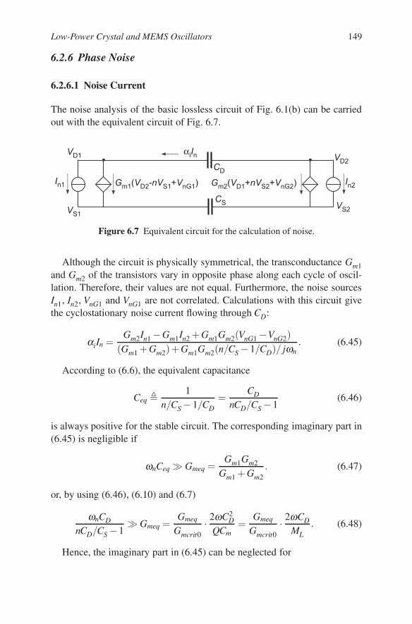
Low-Power Crystal and MEMS Oscillators 149
6.2.6 Phase Noise
6.2.6.1 Noise Current
The noise analysis of the basic lossless circuit of Fig. 6.1(b) can be carriedout with the equivalent circuit of Fig. 6.7.
;)$:
;
$
;)$:
α
$$
;
;
Figure 6.7 Equivalent circuit for the calculation of noise.
Although the circuit is physically symmetrical, the transconductance Gm1and Gm2 of the transistors vary in opposite phase along each cycle of oscil-lation. Therefore, their values are not equal. Furthermore, the noise sourcesIn1, In2, VnG1 and VnG1 are not correlated. Calculations with this circuit givethe cyclostationary noise current flowing through CD:
αiIn =Gm2In1 −Gm1In2 + Gm1Gm2(VnG1 −VnG2)
(Gm1 + Gm2)+ Gm1Gm2(n/CS −1/CD)/ jωn. (6.45)
According to (6.6), the equivalent capacitance
Ceq 1n/CS −1/CD
=CD
nCD/CS −1(6.46)
is always positive for the stable circuit. The corresponding imaginary part in(6.45) is negligible if
ωnCeq Gmeq =Gm1Gm2
Gm1 + Gm2. (6.47)
or, by using (6.46), (6.10) and (6.7)
ωnCD
nCD/CS −1 Gmeq =
Gmeq
Gmcrit0· 2ωC2
D
QCm=
Gmeq
Gmcrit0· 2ωCD
ML. (6.48)
Hence, the imaginary part in (6.45) can be neglected for

150 6 Alternative Architectures
ωn
ω
(nCD
CS−1
)· Gmeq
Gmcrit0· 2
ML. (6.49)
The right hand term is normally much smaller than unity, therefore this con-dition is fulfilled even for noise frequencies ωn much lower than the oscilla-tion frequency ω . The expression (6.45) can then be approximated by
αiIn =Gm2In1 −Gm1In2 + Gm1Gm2(VnG1 −VnG2)
Gm1 + Gm2. (6.50)
This approximation corresponds to a worst case, since the imaginary termwould reduce the value of αiIn.
Because of the capacitance CS between the two sources, the transconduct-ance of the differential amplifier is slightly reduced. Although this effect canbe (and has been) neglected in the calculation of the amplitude, it creates aphase shift ∆φ between the gate voltages and the drain currents. This phaseshift is given by
tan∆φ =nGm1Gm2
ωCS(Gm1 + Gm2). (6.51)
For small amplitudes, Gm1 = Gm2 = Gmcrit , thus
tan∆φ =nGmcrit
2ωCS=
nCD
CS· 1
ML· Gmcrit
Gmcrit0, (6.52)
where the last form has been obtained by introducing the expression (6.10)of Gmcrit0. This phase shift has a minimum value ∆φ = arctan (1/ML) forCS = nCD and Gmcrit = Gmcrit0 (no loss in the circuit).
For large amplitudes, ∆φ is variable along each cycle (which means thatit participates to the distortion of the drain currents), but we will use the ap-proximation of a constant phase shift given by (6.52), which is the maximumvalue of (6.51).
6.2.6.2 Phase Noise of the Linear Circuit
If the amplitude is very small, the circuit remains linear, and the phase noisecan be calculated as explained in Section (3.7.1). The noise voltage Vn acrossCD is obtained from (6.50) with αi = 1 (stationary noise), VG1 = VG2 = 0(since the 1/f gate noise voltage cannot be transposed around the oscillationfrequency) and Gm1 = Gm2 = Gmcrit :
Vn =In1 − In2
2 jωCD. (6.53)

Low-Power Crystal and MEMS Oscillators 151
If the noise currents are solely the channel noise of the transistors, theirspectra are given by (3.60). The noise spectrum of Vn can then be expressedas
SV 2n
= 2kT nγtGmcrit
(ωCD)2 = 4kT nγtRm · Gmcrit
Gmcrit0, (6.54)
where the second form has been obtained by introducing the expression(6.10) of the critical transconductance for the lossless circuit.
The small-amplitude noise excess factor due to the channel noise of theactive transistors is then obtained by inspection of Fig. 3.7:
γ0 =SV 2
n
4kT Rm= nγt
Gmcrit
Gmcrit0, (6.55)
where Gmcrit/Gmcrit0 is the increase of critical transconductance due to pos-sible losses.
6.2.6.3 Phase Noise due to White Channel Noise in the Nonlinear TimeVariant Circuit
For a large amplitude of oscillation, the voltage Vin across CD remains ap-proximately sinusoidal but the drain currents are distorted. From (6.50) and(3.60), the spectrum of the cyclostationary noise current injected in CD isthen
α2i SI2
n=
G2m2SI2
nD1+ G2
m1SI2nD2
(Gm1 + Gm2)2 = 4kT nγtGm1Gm2
Gm1 + Gm2. (6.56)
Notice that the simplification in the second form is made possible by the in-troduction of the channel noise sources of the two transistors. This is possiblesince the values of α2
i corresponding to each source will be simply added inthe calculation of Γ 2
i .Neglecting the effect of CS, the drain currents in weak inversion can be
expressed as
ID1 =2I0
1+ evin sinφ and ID2 =2I0
1+ e−vin sinφ , (6.57)
where vin is the normalized voltage amplitude defined by (6.31) and φ = ωt.The corresponding transconductances in saturation are thus given by (3.54):
Gm1 =2I0
nUT (1+ evin sinφ )and Gm2 =
2I0
nUT (1+ e−vin sinφ ), (6.58)

152 6 Alternative Architectures
Using (6.33) to replace I0 by I0critmin, these expressions can be introduced in(6.56), which gives
α2i SI2
n= 2γtqI0critmin ·
vin
2fw(vin)︸ ︷︷ ︸S
I2n
· 42+ evin sinφ + e−vin sinφ︸ ︷︷ ︸
α2i
. (6.59)
According to (3.34), the mean squared RMS value of the effective impulsesensitivity function (ISF) is thus, for weak inversion
Γ 2i = cos2 (φ + ∆φ)α2
i =1
2π
∫ 2π
0
4cos2 (φ + ∆φ)2+ evin sinφ + e−vin sinφ dφ , (6.60)
where ∆φ is the phase shift approximated by (6.52). The phase noise spec-trum is then obtained by introducing the above values of SI2
nand Γ 2
i in (3.33),which results in
Sφ 2n
= Sφ 2n 0 ·
vin
fw(vin)·Γ 2
i , (6.61)
where
Sφ 2n 0 =
γtqI0critmin
2(CD|Vin|)2∆ω2 ·(
Cm
CD
)2
, (6.62)
or, by introducing (3.54), (6.10) and (2.3), and knowing that CDVin = Im/ω :
Sφ 2n 0 =
γtnkT ω2
|Im|2Q2Rm∆ω2 ·Gmcrit
Gmcrit0. (6.63)
Comparing this result with (3.29) gives the expression (6.55) of the noiseexcess factor γ0 for small amplitudes, which was obtained from the linearmodel.
For larger amplitudes, according to (6.61), the noise excess factor is
γ = γ0 ·vin
fw(vin)·Γ 2
i . (6.64)
This result is plotted in Fig. 6.8 for ∆φ = 0 and ∆φ = 0.4.As can be seen, in weak inversion γ remains constant with the amplitude
if ∆φ = 0. If ∆φ = 0, it decreases when the amplitude increases, but onlyslightly even for a large phase shift ∆φ = 0.4.
In strict strong inversion the two drain currents are given by (6.34). Thetransconductance variations can thus be obtained by introducing these cur-rents in (3.56), which gives

Low-Power Crystal and MEMS Oscillators 153
?3
# , + +
)"#55
) >
&,' '
("
γ/γ&
&,'
&.
&.'
∆φ #∆φ #& ?3
*
Figure 6.8 Variation of the noise excess factor with the drain-to-drain amplitude.The results for strong inversion are based on the approximation IC = IC0.
Gm1(2) =
√I0Ispec
nUT
√1∓mvd sinφ
√2− (mvd sinφ)2. (6.65)
Thus, from (6.56):
α2i SI2
n= 2nγt kT ·
√I0Ispec
nUT·α2
i , (6.66)
with
α2i =
21√
1+mvd sinφ√
2−(mvd sinφ)2+ 1√
1−mvd sinφ√
2−(mvd sinφ)2
. (6.67)
We do not have a closed form expression for the variation of I0 with theamplitude of oscillation. Indeed, both mvd and IC depend on I0 in (6.39). Weshall neglect these dependencies, and approximate IC by IC0.
By using (6.39) to replace I0 by I0crit and (3.56) to express Gmcrit fromI0crit , (6.66) becomes
α2i SI2
n=
SI2n0︷ ︸︸ ︷
2nkT γtGmcrit
√√2mvd
fs(mvd)︸ ︷︷ ︸S
I2n
α2i , (6.68)
According to (3.34), the squared RMS value of the effective impulse sens-itivity function (ISF) is

154 6 Alternative Architectures
Γ 2i =
12π
∫ 2π
0cos2 (φ + ∆φ)α2
i dφ , (6.69)
where ∆φ is the phase shift between gate voltage and drain current approx-imated by (6.52).
For small amplitudes, SI2n
= SI2n0
, α2i = 1 and therefore Γ 2
i = 0.5. Intro-
ducing these values in (3.33) gives, as could be expected, the phase noisespectrum Sφ 2
n 0 obtained for weak inversion and by given (6.63), and the noiseexcess factor γ0 given by (6.55).
For large amplitudes:
γ = γ0 ·2
√√2mvd
fs(mvd)·Γ 2
i . (6.70)
This variation of γ is also plotted in Fig. 6.8 for various values of IC0, usingthe definition (6.35) of mvd (with the approximation IC = IC0).
These results do not include the additional noise due to the biasing cir-cuitry and to losses. But they already include in γ0 the increase of transcon-ductance Gmcrit/Gmcrit0 due to losses.
6.2.6.4 Phase Noise Due to 1/f Flicker Noise
According to the simple model introduced in Section (3.8), the flicker noiseof each of the two transistors can be modelled by a noise voltage VnG, with aspectral density given by (3.62).
The expression (6.45) of the noise current flowing through CD shows thatthe function weighting the noise voltages VnG1 and VnG2 is symmetrical withrespect to Gm1 and Gm2. For this reason the mean value of the ISF givenby (3.34) is zero. Hence, no 1/f noise is transferred around the oscillationfrequency if the noise source is a bias independent noise voltage at the gates(which corresponds to a drain current noise spectral density proportional tothe square of the transconductance).
But this model is an approximation. Let us introduce a more general modelby defining a drain current noise spectral density
SI2nD1/ f =
Fa
ωn
(Gm
Ga
)a
, (6.71)
where Ga is the value of Gm for which the spectrum density has the valueFa/ωn. Considering the noise of transistor T1 only, the resulting cyclosta-tionary noise spectrum is then, from (6.50):
Low-Power Crystal and MEMS Oscillators 155
α2SI2n=
(Gm2
Gm1 + Gm2
)2 Fa
ωn
(Gm1
Ga
)a
. (6.72)
In weak inversion, the transconductance is given by (6.58) or, by using(6.33) to replace I0 by its critical value I0critmin = nUT Gmcrit :
Gm1 =2Gmcrit
1+ evin sinφ · vin
2fw(vin)and Gm2 =
2Gmcrit
1+ e−vin sinφ · vin
2fw(vin). (6.73)
Introducing these expressions in (6.72) yields
α2SI2n=
Fa
ωn
(2Gmcrit
Ga
)a (vin
2fw(vin)
)a
︸ ︷︷ ︸Kfi/ωn
(1+ evin sinφ)2−a
(2+ evin sinφ + e−vin sinφ )2
︸ ︷︷ ︸α2
i
, (6.74)
where Kf i/ωn is the power spectrum of a fictitious source of stationary flickernoise current.
The average value of the effective ISF is thus
Γi = αi cos (φ + ∆φ) =1
2π
∫ 2π
0
(1+ evin sinφ)1−a/2
cos (φ + ∆φ),2+ evin sinφ + e−vin sinφ dφ .
(6.75)which is equal to zero for ∆φ = 0. Using the decomposition cos (φ + ∆φ) =cosφ cos∆φ − sin φ sin∆φ , the dependency on ∆φ can be made more expli-cit:
Γi =−sin∆φ
2π
∫ 2π
0
(1+ evin sinφ)1−a/2
sin φ2+ evin sinφ + e−vin sinφ dφ . (6.76)
For a very small amplitude vin 1, this ISF becomes
Γi0 = −1−a/2
23+a/2vin sin∆φ . (6.77)
Furthermore, for very small amplitudes 2fw(vin) = vin, thus from (6.74):
Kf i0 = Fa
(2Gmcrit
Ga
)a
. (6.78)
The phase noise spectrum for very small amplitude is then obtained by in-troducing (6.77) and (6.78) in (3.36) with Ci = CD and Vi = Vin, which gives
Sφ 2n 0 = 2
((1−a/2)Cm sin∆φ
8nUTC2D
)2 (Gmcrit/Ga)aFa
∆ω3 , (6.79)

156 6 Alternative Architectures
where a factor 2 has been introduced to include the noise of the secondtransistor T2. This result can be further simplified by using the expression(6.10) of the lossless critical transconductance Gmcrit0 = I0crit0/(nUT ), whichyields:
Sφ 2n 0 =
((1−a/2)ω sin∆φ
QI0critmin0
)2 (Gmcrit/Ga)aFa
8∆ω3 , (6.80)
where I0critmin0 is the critical bias current for the lossless circuit. Notice thatif the flicker noise of the transistor is characterized at the critical transcon-ductance, then Ga = Gmcrit and the expression is further simplified.
As could be expected, the phase noise cancels for a = 2, which corres-ponds to the model (3.62) that assumes a bias-independent noise voltage atthe gate. This situation is approached when the transistors operate at the up-per limit of weak inversion [18].
For large amplitudes, Kf i0 is multiplied by [vin/(2fw)]a according to (6.74)
and Γi0 is replaced by Γi given by (6.76). Thus:
Sφ 2n
= Sφ 2n 0
(Γi
Γi0
)2 (vin
2fw(vin)
)a
. (6.81)
This variation is represented in Fig. 6.9 for several values of a.
&'
.#
+ , ' -
&
&,
&+
&
&
)"#
) >
%∆
ω (
φ
φ
?3
Figure 6.9 Variation of the 1/∆ω3 noise due to flicker noise with the amplitude(transistors in weak inversion). The noise spectrum for very small amplitudes Sφ 2
n 0is given by (6.80). The parameter a defined in (6.71) represents the dependency ofthe drain current flicker noise on the transconductance.

Low-Power Crystal and MEMS Oscillators 157
Now, it should be remembered that these results for flicker noise are basedon the expression (6.50) of the cyclostationary noise, in which the imaginarypart of the full expression (6.45) has been neglected. For frequencies ωn thatare to small to fulfill condition (6.49), the noise is reduced, thus the phasenoise spectrum stops increasing with 1/∆ω3.
6.2.7 Practical Implementations
To avoid the need to increase the supply voltage in order to reduce the losses,the parallel resonance oscillator can be biased as illustrated in Fig. 6.10(a).The biasing resistors are replaced by current sources I0 and the common-
>
;
$
<
;
$
<
>
> >
>
>>
>
Figure 6.10 Practical biasing of the parallel resonance oscillator.
mode drain voltage of the active transistors Ta is controlled by a feedbackloop through the biasing transistors Tb. The role of the resistors is to ex-tract this common-mode voltage, hence their value can be very large withoutincreasing the minimum supply voltage. At the DC bias point, the two tran-sistors Ta and Tb in series are equivalent (by symmetry) to a single transistorhaving is gate connected to its drain. Hence, the common mode voltage isthe gate voltage corresponding to a drain current equal to I0.
Now, transistors Tb are not saturated since they have the same gate voltageas Ta. According to (3.50) and (3.40), their drain (trans)conductance is pro-portional to the source transconductance of the active transistors:

158 6 Alternative Architectures
Gmdb = Ks ·Gmsa with Ks Ispecb
Ispeca, (6.82)
since the drain voltage of Tb is the source voltage of Ta. This drain con-ductance corresponds to a loss conductance GS = Gmdb/2 in parallel withCS. But this loss conductance is now proportional to the transconductanceGm = Gmsa/n of the active transistors, with the consequence that the locusof Zc(Gm) is no longer a circle. This locus can be computed by introducing
1/ZS = jωCS + KsnGm/2 (6.83)
in the expression (6.11) of the circuit impedance. The result is illustrated inFig. 6.11 for two values of the ratio Ks of specific currents. As can be seen,
+ , + ,
)
ω;ω;
+#&
+#&
+#&
+#
)#&$#;
ω;! ω;
+#&
Figure 6.11 Normalized locus of circuit impedance Zc(Gm) for the oscillator ofFig. 6.10(a), with negligible losses due to resistors R. The locus for the losslesscircuit is shown in dotted line.
the losses due the biasing transistors Tb are negligible for small values ofthe transconductance Gm, but the loci depart from the lossless case when Gm
increases. For this particular (but typical) case with n = 1.3 and CS = CD, themaximum value of negative resistance is not reduced for Ks = 0.01, but it isreduced by about 50% for Ks = 0.1.
Now, for the calculation of the loci shown in Fig. 6.11 the value of resistorR was assumed to be very large. But to maintain a stable bias point this valuehas an upper limit. Indeed, because of the DC path provided by transistors

Low-Power Crystal and MEMS Oscillators 159
Tb, the circuit can become bistable. The active transistor Ta has its sourcedegenerated by the drain (trans)conductance of Tb given by (6.82), hence itsequivalent gate transconductance at low frequencies is
Gmequ =GmsaGmdb
n(Gmsa + Gmdb)=
Gm
1+ 1/Ks. (6.84)
Bistability is avoided if the voltage gain GmequR of each branch is smallerthan unity, which results in the following condition for stability of the biaspoint:
R <1+ 1/Ks
Gmmax, (6.85)
where Gmmax is gate transconductance of Ta alone obtained at the maximumvalue of bias current I0. Hence, Ks must be very small to limit the losses dueto R, especially if I0 I0crit at start-up.
To avoid using resistors, the gates of the biasing transistors Tb can beconnected as shown in Fig. 6.10(b) [25]. The DC bias point remains thesame, since by symmetry the two drains are at the same (common mode)potential. But the transistors Tb are now active, with a gate transconductanceGmb. The circuit impedance without the parallel capacitance CD becomes
Zc0 =1+ Ks + 2
nGmZS
Gmb2 − 1
nZS− KsGm
2
. (6.86)
Now, the relationship between Gmb and the gate transconductance Gm ofthe main active transistors depends on their mode of operation. Knowing thatTa and Tb have the same gate voltage with Ta saturated, their components ofdrain current can be expressed as
IRb = KsIFa = KsI0 and IFb = I0 + IRb = (1+ Ks)I0. (6.87)
If both transistors are in strong inversion, the corresponding values of gatetransconductance are obtained from (3.53) and (3.51):
Gm =
√I0Ispeca
nUTand Gmb =
√I0Ispecb
(√1+ Ks−
√Ks
)
nUT, (6.88)
and their ratio is
Gmb
Gm=
√Ks(1+ Ks)−Ks (in strong inversion). (6.89)

160 6 Alternative Architectures
This ratio tends to√
Ks for Ks 1 and never exceeds 0.5.The introduction of (6.89) in (6.86) gives Zc0(Gm), which can be com-
bined with ZD according to (6.11) to obtain the full circuit impedanceZc(Gm). The analytical result is too complicated to be expressed, but the nu-merical calculation can be carried out step by step. The result for the losslesscase (GD = GS = 0) is plotted in full lines in Fig. 6.12(a) for two values ofthe ratio Ks of specific currents.
+#&
+#&
+#&ω;
'
'
#
#
!
+#&
'
&
'ω;!
ω;
&
&,
)&
ω;
?3*
&
)#&$#;
+#&
+#&
+#&
+#&
Figure 6.12 (a) Normalized locus of circuit impedance Zc(Gm ≥ 0) for the oscil-lator of Fig. 6.10(b); full lines: for all transistors always in strong inversion; dottedlines: for all transistors always in weak inversion. The circular lossless locus for thebasic circuit of Fig. 6.1(b) is shown in fine dotted line for comparison. (b) Variationof the real and imaginary parts with the normalized transconductance.
Compared to the circular locus of the basic circuit (shown in fine dot-ted line), the maximum negative resistance is reduced by the activity of thebiasing transistors.
If the transistors are in weak inversion, the gate transconductance onlydepends on the total drain current that is the same for the two transistors,hence Gmb ≡ Gm. The degradation is increased due to the larger Gmb, asshown by the corresponding results in dotted lines. However, as can be seenin part (b) of the figure, as long as the negative resistance Rn = −Re(Zc)is much smaller than its maximum value, it always depends linearly on thetransconductance with
Rn = − Gm
2(ωCD)2 , (6.90)

Low-Power Crystal and MEMS Oscillators 161
thereby resulting in the critical condition for oscillation Gmcrit0 for thelossless circuit given by (6.10).
Furthermore, for |Rn| |Rn|max, the imaginary part remains close to -1,thus the expression (6.17) of the frequency pulling is not affected.
Now, the plots of Fig. 6.12 have been obtained by assuming the all tran-sistors are always in weak or in strong inversion. In reality, all transistorsare in weak inversion at very low currents (i.e. for very low values of thetransconductance), and all transistors are in strong inversion for very highcurrents. The transition occurs at a level of current that depends on the spe-cific currents Ispeca and Ispecb, according to the general equation (3.50) forthe transconductance. No analytical expression of Zc(Gm) can be found inthe general case.
*
?3
&
&
+#& *
*
?3
?3
&&
+#
&
&
'
&
&,
&
'
)
ω;
ω;!
ω;
ω;
)#&$#;+#&
+#
Figure 6.13 (a) Normalized locus of circuit impedance Zc(Gm ≥ 0) for the oscil-lator of Fig. 6.10(b) with transistors Ta in weak inversion and Tb in strong inversioncharacterized by parameter Kl (defined by (6.92)). Curves in dotted lines are for theasymptotic cases of all transistor in weak and in strong inversion. (b) Variation ofthe real and imaginary parts with the normalized transconductance.
To minimize the value of the critical bias current I0crit , the active tran-sistors Ta must be operated in weak inversion, whereas the biasing transist-ors Tb should be in strong inversion to reduce their transconductance. Theirtransconductance given by (6.88) can then be expressed as a function of themain transconductance Gm = I0/(nUT :

162 6 Alternative Architectures
;
$
<
> >>>
>
>
> >
>>
>
:
:
:
:
/
Figure 6.14 Parallel resonance oscillator with amplitude regulation.
Gmb
ωCD=
√Kl ·
√Gm
ωCD
(√1+ Ks−
√Ks
), (6.91)
where Kl is a parameter defined by
Kl Ispecb
ωCDnUT(6.92)
that characterizes the level of the specific current.This new expression of Gmb can again be combined with (6.86) and (6.11)
to obtain Zc(Gm). An example with Ks = 0.01 and several values of Kl isillustrated in Fig. 6.13. The results are between the extreme cases of weakand strong inversion for both transistors.
The amplitude of oscillation can be regulated by delivering the bias cur-rent from the regulator discussed in Section (5.2). A more compact solutionis depicted in Fig. 6.14 [25].
Two pairs of transistors matched to the main pairs Ta −Tb have been ad-ded. The same current I0 flows through all four branches. The common modevoltage of the main pairs is extracted by transistors Tr1 and Tr2 matched totheir biasing transistor Tcr.
The pair Ta3 −Tb3 is identical to the main pair. Hence, in absence of os-cillation, all four gates nodes G1 to G4 are at the same potential. But thespecific currents of the transistors of the fourth pair are Kw times larger than

Low-Power Crystal and MEMS Oscillators 163
those of the main pair, which must be compensated by a voltage drop RI0across resistor R.
If all pairs are in weak inversion, a stable solution without oscillation isreached as in the regulator of Section (5.2) for
I0 = I0start =UT
RlnKw. (6.93)
If this current is larger than the critical current, the oscillation starts growing,but unlike for the single transistor of the Pierce oscillator, the common modevoltage remains essentially constant at constant I0. Hence no amplitude reg-ulation would occur if the common mode would be extracted by linear res-istors instead of transistors. But the nonlinearity of the transistor produces avoltage drop at the node G4 given by (5.41) with |V2| = 0 and |V1| replacedby |Vin|/2:
∆VG0 = −UT ln [IB0(|Vin|/2UT)]. (6.94)
The transfer function of the regulator is then obtained by adding ∆VG0/n toUT lnKw in the expression (6.93) of the current, which yields:
I0
I0start= 1− ln [IB0(|Vin|/2UT)]
n lnKw, (6.95)
where |Vin| is the gate to gate amplitude of oscillation. This function is plottedin Fig. 6.15 for several values of ratio Kw.
!
Figure 6.15 Regulation curves for the circuit of Fig. 6.14 with all transistors oper-ated in weak inversion. The small drain voltage shift due to the distortion of draincurrent is neglected.

164 6 Alternative Architectures
The loss conductance due to transistors Tr (for the fundamental fre-quency) can be obtained as discussed in Section 5.1.5, with Vin/2 acrosseach transistor:
G1 ≡ G(1) = G02IB1(|Vin|/2UT)
|Vin|/2UT. (6.96)
With the specific current of the biasing transistor Tcr Kr-times larger than thatof one of the transistors Tr, the small-signal value G0 of this loss conductanceis now
G0 =I0
2KrUT. (6.97)
6.3 Symmetrical Oscillator for Series Resonance
6.3.1 Basic Structure
The basic symmetrical oscillator circuit intended for series resonators isshown in Fig. 6.16(a). It is based on a current stable negative resistancecircuit developed for vacuum tubes (Fig. 69e, page 82 of [15]). A ver-sion with bipolar transistors was used in early developments of electronicwatches [26]. Each of the two cross-coupled transistors is biased by a cur-
!
"
#
$" "
"
% &
"
#
!
!
"
%&
"
%!&
Figure 6.16 Symmetrical oscillator for series resonator; (a) complete oscillator; (b)negative resistance circuit without bias sources; (c) small-signal general equivalentcircuit.

Low-Power Crystal and MEMS Oscillators 165
rent source I0 and is loaded by a resistor of value RL/2. As long as the circuitremains symmetrical, the effect of all capacitors at the drains can be repres-ented by a single load capacitance CL between the two drains. The resonatorconnects the sources of the two transistors. The transistors are assumed to bein the same local substrate.
6.3.2 Linear Analysis
6.3.2.1 Circuit Impedance in the General Case
To calculate the small-signal circuit impedance Zc, the circuit may be repres-ented as in Fig. 6.16(b), after removing the biasing elements. Capacitance CPis the capacitance C0 of the quartz resonator considered as a dipole definedby (2.1), augmented by the parasitic capacitors in the circuit.
At frequencies for which the capacitors can be neglected, the circuit im-pedance is easily calculated to be
Zc|ω=0 =2−GmRL
Gms=
1n(2/Gm −RL), (6.98)
where Gms is the source transconductance, which is n times larger than thegate transconductance Gm, according to (3.55). Hence, unlike the Pierce os-cillator, this circuit provides a DC negative resistance. It becomes DC un-stable, that is bi-stable, when it is connected to a resistor of value smallerthan this negative resistance.
But it can also become AC unstable, i.e. an oscillator, when it is connectedto the sole capacitance CP. The AC circuit impedance Zc0 without CP is givenby
Zc0 =2−GmZL
Gms=
1n(2/Gm −ZL), (6.99)
where the load impedance ZL including CL can be expressed as
ZL =RL − jωCLR2
L
1+(ωCLRL)2 . (6.100)
Thus
Zc0 =2
nGm− RL/n
1+(ωCLRL)2 + jωCLR2
L/n1+(ωCLRL)2 . (6.101)
When CP is connected, an oscillation can occur at the frequency for whichIm(ZC0) = 1/(ωCP), that is for

166 6 Alternative Architectures
ω2 =1
CLR2L(CP/n−CL)
. (6.102)
this frequency does not exist if
CL > CP/n, (6.103)
which is a sufficient condition to avoid this parasitic oscillation. But thiscondition is not absolutely necessary, since the real part of Zc0 in (6.101)must be negative at the frequency given by (6.102). This requirement givesthe following necessary condition for no parasitic oscillation:
CL >CP
n
(1− 2
RLGm
), (6.104)
which is reduced to (6.103) for RLGm 1.
"#
! '
# (!)"
ω"#
*
+
"#
Figure 6.17 Loci of circuit impedance Zc/RL for ωRLCP = 0.3 and n = 1.3. Noticethat CL/CP = 0 will produce a parasitic oscillation whereas CL/CP = 1/n corres-ponds to the sufficient condition (6.103) for no parasitic oscillation.
Adding the impedance ZP of the parallel capacitor CP (with possiblelosses) in parallel with Zc0 gives the overall circuit impedance
Zc =ZP(2−GmZL)
2+ Gm(nZP −ZL), (6.105)

Low-Power Crystal and MEMS Oscillators 167
which corresponds to the equivalent circuit of Fig. 6.16(c). It is a bilinearfunction of the transconductance Gm. The corresponding circle in the com-plex plane is plotted in Fig. 6.17 for particular values of ωRLCP and slopefactor n, and for various values of the capacitance ratio CL/CP.
6.3.2.2 Particular Case with CL = CP/n
The analytic expressions of the real and imaginary parts of Zc are complic-ated, but they can be simplified for the particular (and realistic) case forwhich the sufficient condition (6.103) is just fulfilled, i.e. for CL = CP/n.All the following derivations will be made with this assumption.
The results are then
Re(Zc) =1
ωCP· AB(2B + 2/B−A)
4+(2B−A)2 (6.106)
Im(Zc) =1
ωCP· 4(AB−B2−1)
4+(2B−A)2 , (6.107)
where
A Gm
ωCL=
nGm
ωCPand B ωCLRL = ωCPRL/n. (6.108)
The locus of the normalized circuit impedance for positive values oftransconductance Gm is plotted in Fig. 6.18 for various values of B (thusof RL for ωCP/n constant). This locus is a circle of radius (1+ B2)/2 that isalways centered on the imaginary axis.
For Gm = 0 the transistors are not active and the impedance is that of theparallel capacitance CP.
The value of transconductance needed to obtain a negative resistance isobtained from (6.106):
Gm > Gmlim =2(1+ B2)
RL=
2ωCP
n(B + 1/B). (6.109)
The imaginary part of Zc at the limit of negative resistance (for Re(Zc) = 0)is
Im(Zc)lim = Im(Zc)|Re(Zc)=0 =B2
ωCP= BRL/n. (6.110)
Eliminating B between these two equations gives

168 6 Alternative Architectures
ω
ω!
/#&
&
&
&,
&+
&
*/
#
#
7#%)
ω
/
Figure 6.18 Locus of the normalized circuit impedance ωCPZc for several valuesof B = ωCPRL/n. The locus of −Zm(p) for a particular value of motional resistanceRm is represented in dotted line.
Gmlim =2ωCP
n
(√ωCPIm(Zc)lim +
1√ωCPIm(Zc)lim
.
). (6.111)
If the maximum value of negative resistance (−Rn)max is much larger thanthe motional resistance Rm of the resonator (as depicted in dotted line inFig. 6.18), that is if
B ωCPRm = 1/MD (6.112)
(with MD defined by (2.22)), then the imaginary part of Zc can be approxim-ated by (6.110). According to (4.3), the amount of frequency pulling at thecritical condition for oscillation is then
pc∼= − Cm
2CPB2. (6.113)
The comparison with (4.21) shows that CP/B2 plays the same role as Cs +C3 in the Pierce oscillator. But B depends on a resistance, which is usuallymuch less precise and stable with the temperature than a capacitor in anintegrated circuit. Another important difference is that pc is now negative:the frequency of oscillation is lower than the mechanical resonant frequencyof the resonator.
For Gm very large, (6.106) gives:

Low-Power Crystal and MEMS Oscillators 169
Zc|Gm=∞ = − BωCP
= −RL/n. (6.114)
This is the maximum possible value of negative resistance that can be ob-tained for B ≤ 1. But for B > 1, a larger negative resistance can be obtained,corresponding to the radius (1 + B2)/2 of the circle, as can be observed inFig. 6.18:
(−Rn)max =1+ B2
2ωCP=
B + 1/B2n
RL (for B > 1) (6.115)
for a value Gmopt of the transconductance given by
Gmopt =ωCP
n· 2(B2 + 1)
B−1. (6.116)
For Gm > Gmopt , the slope of the locus becomes negative, and no stable solu-tion exists, as was the case for solution B in Fig. 4.4. Therefore, the only use-ful range of transconductance for B > 1 is between Gmlim given by (6.109)and Gmopt .
The critical transconductance for oscillation is the value of Gm for whichRe(Zc) = Rn = −Rm. It is obtained by solving (6.106) with respect to A =nGm/(ωCP). This gives:
Gmcrit =ωCP
n· 1+ B2 −2BωCPRm +
√(1+ B2)2 − (2ωCPRm)2
B−ωCPRm. (6.117)
This critical transconductance can also be expressed as
Gmcrit = Gmlim + ∆Gm(Rm). (6.118)
For Rm (−Rn)max, ∆Gm can be approximated linearly by
∆Gm∼=
2ω2C2P
nB2 Rm =2nRm
R2L
=ωCP
n· 1
Q|pc|, (6.119)
where |pc| has been obtained from (6.113). The combination of (6.118),(6.109) and (6.119) gives an approximation of the critical transconductance
Gmcrit∼= 2ωCP
n
(B +
1B
+1
2Q|pc|
). (6.120)
It is worth noticing that, as long as Q|pc| is sufficiently large, it has no effecton the critical transconductance:

170 6 Alternative Architectures
Gmcrit = Gmlim =2ωCP
n(B + 1/B) for 2Q|pc|
B1+ B2 . (6.121)
Unlike for the Pierce oscillator (see (4.26)), the critical transconductance isnot reduced by a large value of quality factor Q. But it still depends on pc
through the design parameter B (i.e. through the choice of load resistanceRL).
The dependency of the various important values discussed above on theparameter B is plotted in Fig. 6.19.
'
+
,
ω!
ω"
)
ω
)
ω
/#ω7%)
)
ω∆
&
Figure 6.19 Normalized values of Gmlim, −Rn/∆Gm, Im(Zc) at Gmlim (thus forRn = 0), (−Rn)max and Gmopt as functions of parameter B.
For a fixed value of parallel capacitance CP, the limit value Gmlim of thetransconductance has a minimum for B = 1:
Gmlimmin= 4ωCP/n = 4/RL for B = 1. (6.122)
For B > 1 the imaginary part of Zc increases dramatically, thereby in-creasing the amount of frequency pulling given by (6.113). The only reasonto choose B > 1 would thus be to produce a very large value of negativeresistance, at the cost of an increase transconductance and an increase of pc.
As already pointed out, B = 1 corresponds to a minimum value of limittransconductance Gmlim. The corresponding locus of Zc(Gm) is illustrated inFig. 6.20(a) with the real and imaginary parts in Fig. 6.20(b).
The exact critical transconductance given by (6.117) becomes
Gmcrit |B=1 =2ωCP
n
(1+
√1+ ωCPRm
1−ωCPRm
), (6.123)

Low-Power Crystal and MEMS Oscillators 171
ω
ω
ω
ω
ω
! ω
Figure 6.20 Normalized circuit impedance ωCPZc for CL = CP/n and minimumlimit transconductance (B = 1). The approximation (6.120) of Gmcrit (Rn) is alsoshown in dotted line.
"
! ω
"
"
#
ω
ω
ω
"
Figure 6.21 Normalized circuit impedance ωCPZc for CL = CP/n and B = 0.5.
and the exact amount of frequency pulling obtained by introducing (6.107)in (4.3) with B = 1 is
pc|B=1 = − Cm
2CP
√1− (ωCPRm)2. (6.124)
For B < 1, The maximum negative resistance is decreased according to(6.114). The imaginary part of Zc decreases rapidly with B (thereby decreas-ing the amount of frequency pulling pc), at the cost of an increase of the

172 6 Alternative Architectures
necessary value of transconductance. But this increase can be small for alarge reduction of |pc|. For example, choosing B = 0.5 results in just a 25%increase of Gmlim whereas pc is decreased by a factor 4. This particular casein illustrated in Fig. 6.21.
6.3.2.3 Relative Oscillation Currents
At the critical condition for oscillation, the frequency pulling is approxim-ately given by (6.113). Thus the motional impedance expressed by (2.8) be-comes
Zm|p=pc = Rm − jB2
ωCP= Rm(1− jMDB2), (6.125)
where MD is the factor of merit defined by (2.22).The AC component of drain current I1 is split between the motional cur-
rent Im and the current IP through the parallel capacitance CP according to
IP
Im= jωCPZm = B2 +
jMD
∼= B2, (6.126)
and the AC component of drain current I1 is related the motional current Im
byI1
Im= 1+ jωCPZm = (1+ B2)+
jMD
∼= (1+ B2). (6.127)
6.3.3 Nonlinear Analysis
As soon as the transconductance Gm exceeds the critical value given by(6.117) (or by its approximation (6.120)), the amplitude of oscillation grows.The drain current of each transistor can then be expressed as
ID = I0 + I1, (6.128)
where I0 is the DC component imposed by the biasing current source, and I1is the AC oscillatory current.
According to (6.126), if B 1 and MD 1 most of the AC currentI1 flowing through the transistors is the motional current of the resonator.Hence I1 remains approximately sinusoidal. Therefore the gate voltage re-mains also sinusoidal, but the source voltage VS is distorted by the nonlinear

Low-Power Crystal and MEMS Oscillators 173
transfer function of the transistors. The effective transconductance is reducedand more bias current I0 is needed to further increase I1, until it reaches itsmaximum value equal to I0 (100% modulation of bias current I0).
The variation of the amplitude of oscillation with the bias current canbe obtained by an approach similar to that used for the Pierce oscillator inSection 4.3.3. However, the source of the transistor is not grounded and thedrain current is modulated by gate and source voltage variations. Accordingto (3.40), the drain current in saturation depends on a control voltage
Vc VG −VT0 −nVS (6.129)
of normalized amplitude
vc |Vc|nUT
(6.130)
The corresponding transconductance is equal to the gate transconductanceat the same value of current:
dID
dVc=
dID
dVG= Gm (6.131)
Let us assume that the AC component of drain current is perfectly sinusoidal,with
ID = I0(1+ mi sinΦ), (6.132)
wheremi |I1|/I0 (6.133)
is the index of current modulation.The value of Gm for the fundamental frequency can be expressed as
Gm(1) =|I1|
|Vc(1)|=
miI0
nUT vc(1), (6.134)
where |Vc(1)| is the amplitude of the fundamental component of Vc and vc(1)its value normalized to nUT . Stable oscillation is obtained when Gm(1) equalsthe critical value of Gm
Gmcrit =I0critmin
nUT, (6.135)
where I0critmin is the minimum possible value of I0 needed to produce Gmcrit(that is in weak inversion). Equating (6.134) with (6.135) yields
I0
I0critmin=
vc(1)
mi. (6.136)

174 6 Alternative Architectures
In weak inversion, the saturation drain current ID = IF given by (3.42) canbe rewritten
ID = Ispec exp(vc) or vc = lnID
Ispec= ln
I0
Ispec+ ln(1+ mi sinφ) (6.137)
The fundamental component of vc is thus given by
vc(1) =1π
∫ 2π
0ln(1+ mi sinΦ)sin Φ ·dΦ . (6.138)
Introducing this result in (6.136) yields the relation between the bias currentI0 in weak inversion and the index of modulation mi. It is plotted in Fig. 6.22.
+ ,
&
&
&+
&,
&
?3
#,++
/#&'
!"
$
< %
/#&
Figure 6.22 Index of current modulation as a function of the bias current. The para-meter IC0 is the inversion coefficient at the critical bias current I0crit . Circles aresimulation results of |Im|/I0 in weak inversion, showing that, except for B 1, thedistortion of the drain current cannot be neglected when saturation is approached.
In strong inversion, the saturation drain current ID = IF given by (3.43)can be written
ID = Ispec
(vc
2
)2or vc = 2
√ID
Ispec. (6.139)
As for the Pierce circuit, the level of inversion can be characterized by theinversion coefficient at the critical current for oscillation:

Low-Power Crystal and MEMS Oscillators 175
IC0 I0crit
Ispec(6.140)
The fundamental component of vc can then be expressed as
vc(1) =
√I0
I0critIC0 ·hs(mi), (6.141)
with
hs(mi) =2π
∫ 2π
0
√(1+ mi sinΦ) · sinΦ ·dΦ (6.142)
According to (3.56), the critical current in strong inversion is related to itsminimum value (reached in weak inversion) by
I0crit = I0critmin
√IC0, (6.143)
therefore (6.141) becomes
vc(1) =
√I0
I0critmin· 4√
IC0 ·hs(mi), (6.144)
Introducing this result in (6.136) and solving for I0/I0critmin gives finally
I0
I0critmin=
√IC0 ·
(hs(mi)
mi
)2
, (6.145)
which is plotted in Fig. 6.22 for several values of IC0. As can be seen inthis figure, |I1| saturates to the value I0 for I0 >
√2I0crit (slightly more in
weak inversion). But a part of I1 flows through the load capacitor CL and thevoltage amplitude at the drain is limited to
|VD(1)| =RLI0
2√
1+ B2. (6.146)
Similarly, a part of I1 is diverted from the resonator itself to flow through theparallel capacitor CP, according to (6.127).
But it must be remembered that this calculation of the amplitude is onlyan crude approximation, since it is based on the assumption that the ACcomponent I1 of drain current is perfectly sinusoidal. In reality, when thesource voltage is distorted, harmonic components of current can flow throughthe parallel capacitance CP and the drain current is distorted.
In practice, except for B 1, nonlinear effects cannot be neglected when|I1| reaches its assumed saturation value I0. This is illustrated by the simu-lation results of |Im|/I0 (for |Rn| RL) represented by circles in Fig. 6.22.
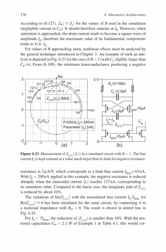
176 6 Alternative Architectures
According to (6.127), |Im| ∼= |I1| for the values of B used in the simulation(negligible current in CP). It should therefore saturate at I0. However, whensaturation is approached, the drain current tends to become a square wave ofamplitude I0, therefore the maximum value of its fundamental componentstends to 4/π · I0.
For values of B approaching unity, nonlinear effects must be analyzed bythe general technique introduced in Chapter 3. An example of such an ana-lysis is depicted in Fig. 6.23 for the case of B = 1 (with CL slightly larger thanCP/n). From (6.109), the minimum transconductance producing a negative
7%#DΩ
7#&'/
#/
#'µ4
#'µ4
#
8
'-&
-&'-&+
.
+
,
-&
-&-
!
5 5CDΩE
5 5C4E
%#3F#4
Figure 6.23 Measurement of Zc(1)(|Ic|) in a simulated circuit with B = 1. The biascurrent I0 is kept constant at a value much larger than its limit for negative resistance.
resistance is 2 µA/V, which corresponds to a limit bias current I0lim= 63nA.With I0 = 200nA applied in this example, the negative resistance is reducedabruptly when the sinusoidal current |Ic| reaches 127nA, corresponding toits saturation value. Compared to the linear case, the imaginary part of Zc(1)is reduced by about 10%.
The variations of Im(Zc(1)) with the normalized bias current I0/I0lim forRe(Zc(1))
∼= 0 has been simulated for the same circuit, by connecting it toa motional impedance with Rm = 0. The result is shown in dotted line inFig. 6.24.
For I0 < 7I0lim, the reduction of |Zc(1)| is smaller than 10%. With the mo-tional capacitance Cm = 2.1 fF of Example 1 in Table 4.1, this would cor-

Low-Power Crystal and MEMS Oscillators 177
&,
&
&
&
&+
+ , +
5 5
?3 #
< %
5 5
5 5
Figure 6.24 Measurements of Zc(1)(I0) and |Ic|(I0) in the simulated circuit ofFig. 6.23(b).
respond to a maximum variation of frequency pulling of 3.5 · 10−5. It startschanging more drastically for larger values of I0.
The same figure shows the variation of the sinusoidal current |Ic| = |Im|with the bias current. The ratio |Ic|/I0 reaches a first plateau that is about4/π higher than what would be calculated by (6.127) for a sinusoidal draincurrent of amplitude |I1| = I0, before further increasing.
6.3.4 Phase Noise
6.3.4.1 Noise Voltage
The effect of the channel noise can be analyzed by means of the equival-ent circuit of Fig. 6.25. Besides the channel noise sources InD1 and InD1 ofthe two transistors, the thermal noise current InR of the load resistance is in-cluded. Calculations on this circuit for the limit case CP = nCL yields thecyclostationary noise voltage across the motional impedance Zm:
αvVn =1n· RLInR +(1+ jBn)(InD1/Gm1 − InD2/Gm2)
(1− xB2n)+ jxBn
, (6.147)
where Bn is the value of B defined in (6.108) with ω replaced by ωn, thefrequency at which the noise is considered. The local variable x is defined by
x 1RL
(1
Gm1+
1Gm2
)(6.148)

178 6 Alternative Architectures
;)$ ;
;
;)$;
7
;
α
#)7
7
$ $
Figure 6.25 Equivalent circuit for noise calculation of the series resonance oscil-lator.
It varies periodically along each cycle of oscillation.Using the expression (3.60) of the spectrum of InD, the spectrum of this
cyclostationary voltage is then
α2v SV 2
n=
4kT RL
n2 · 1+(1+ B2n)nγt x
B2nx2 +(1−B2
nx)2 , (6.149)
6.3.4.2 Phase Noise of the Linear Circuit
For very small amplitudes, the circuit remains linear and only noise frequen-cies close to the oscillation frequency have to be considered, thus αv = 1,Gm1 = Gm2 = Gmcrit and Bn = B. After approximating Gmcrit by Gmlim givenby (6.109), the voltage noise spectral density becomes
SV 2n0
= 4kT RL1+ nγt
n2 (1+ B2). (6.150)
According to Fig. 3.7, the phase noise excess factor at very small amplitudesis obtained after division of the thermal noise spectrum of Rm:
γ0 =1+ nγt
n2 (1+ B2)RL
Rm, (6.151)
showing that γ0 is minimum for B small and for RL close to Rm.

Low-Power Crystal and MEMS Oscillators 179
6.3.4.3 Phase Noise due to White Noise in the Nonlinear Time VariantCircuit
The calculation of phase noise for large amplitudes is made complicatedby the fact that the spectrum of the cyclostationary noise voltage expressedby (6.149) depends on Bn, i.e. on the frequency ωn at which the noise isconsidered. Furthermore, this spectrum depends on the value of x that variesalong each cycle with Gm1 and Gm2, according to (6.148). This variation isillustrated by Fig. 6.26.
) B
) B/#/ω%ω&' & &' &
#&'
,
α87
)#&
Figure 6.26 Spectrum of the cyclostationary noise for various values of x.
To render the problem tractable analytically, we shall assume that thespectrum remains constant at its value at the oscillation frequency by re-placing Bn by B. As can be seen in the figure, this approximation is onlyvalid for ωn ω/B and x not too large. This domain of validity includesnoise frequencies above ω only if B 1 and mi not to close to unity (sincethe peaks of x tend to infinity when mi approaches unity).
The spectrum (3.60) of the cyclostationary voltage is thus approximatedby
α2v SV 2
n=
4kT RL
n2︸ ︷︷ ︸S
V 2n
· 1+(1+ B2)nγt xB2x2 +(1−B2x)2︸ ︷︷ ︸
α2v
, (6.152)
where SV 2n
is the spectrum of a fictitious noise voltage modulated by αv.If the transistors operate in weak inversion, the transconductance is given
by (3.54) and varies cyclically with the drain current according to (6.132):
180 6 Alternative Architectures
Gm1,2 =I0
nUT(1±mi sinφ) = Gmcrit ·
vc(1)
mi(1±mi sinφ), (6.153)
where the second form has been obtained by using (6.136) to replace I0 byits critical value, with vc(1) given by (6.138).
As done previously, the critical transconductance Gmcrit can be approxim-ated by the limit value Gmlim given by (6.109). The local variable x definedby (6.148) then becomes
x =1
1+ B2 ·mi
vc(1)· 1
1−m2i sin2φ
(6.154)
and can be introduced into (6.152) to obtain α2v . The mean square value of
the effective impulse sensitivity function is then given by
Γ 2v = α2
v cos2 (φ + ∆φ) =1
2π
∫ 2π
0α2
v cos2 (φ + ∆φ)dφ , (6.155)
where ∆φ is the phase shift between the current I1 through the transistor andthe motional current Im. Indeed, the peaks of the noise voltage modulationfunction αv coincide with the peaks of current through the transistors. Thus,from (6.127)
tan∆φ =1
MD(1+ B2)(6.156)
Now, SV 2n
in (6.152) is independent of the current modulation index mi.Therefore, according to (3.31), the spectral density of the phase noise due tothe circuit is proportional to Γ 2
v . Thus the variation of the phase noise excessfactor γ is
γγ0
=Γ 2
v
Γ 2v /|mi=0
. (6.157)
Results obtained by introducing (6.154) and (6.152) in (6.155) are plottedin Fig. 6.27 for two values of the normalized bandwidth B. They show thatthe noise excess factor remains approximately constant with the index ofmodulation.
It must be reminded that the approximation by a white noise voltage spec-trum (Bn = B in (6.149)) is only valid for B 1. Otherwise, if the modula-tion factor approaches unity, Gm1 or Gm2 becomes very small in the peaksof oscillation and x defined by (6.148) becomes very large. As illustratedby Fig. 6.26, the noise is then no longer white but is concentrated at lowfrequencies.

Low-Power Crystal and MEMS Oscillators 181
∆φ#&
/#&
& &, & &, &+
&
&+
&
)" γ
γ
9"
∆φ#&
/#&
)#&
Figure 6.27 Variation of the phase noise excess factor with the amplitude of oscil-lation, with transistors operated in weak inversion. These results are calculated withthe approximation of a white noise voltage spectrum across the motional impedanceof the resonator.
6.3.4.4 Phase Noise due to the Flicker Noise of the Active Transistors
As for the parallel resonance oscillator, a bias independent voltage source offlicker noise at the gate (as in the simple model defined by (3.62)) producesno phase noise, due to the symmetry of the circuit. Let us use again themore general model (6.71) for a flicker noise drain current. For the noise oftransistor T1 only, the spectral density of cyclostationary noise voltage acrossthe motional impedance given by (6.147) becomes
α2v SV 2
n=
(1+ B2n)
(1− xB2n)2 + x2B2
n· Fa(Gm1/Ga)a
ωnn2G2m1
. (6.158)
For low-frequency flicker noise, Bn = ωn/ω 1. Furthermore xBn 1, ex-cept when x defined by (6.148) becomes very large in the peaks of oscillation(Gm1 or Gm2 very small). Therefore, (6.158) can be simplified to
α2v SV 2
n=
FaGa−2m1
ωnn2Gaa. (6.159)
In weak inversion, the variation of Gm1 along each cycle is given by (6.153),hence
α2v SV 2
n=
FaGa−2mcrit
ωnn2Gaa·(vc(1)
mi
)a−2
︸ ︷︷ ︸12 ·
Kf vωn
·(1+ mi sinφ)a−2
︸ ︷︷ ︸α2
v
. (6.160)
The spectrum of the fictitious flicker noise voltage modulated by αv is thuscharacterized by

182 6 Alternative Architectures
Kf v = 2Fa ·(
Gmcrit
Ga
)a
· 1n2G2
mcrit
·(vc(1)
mi
)a−2
, (6.161)
where a factor 2 has been introduced to account for the noise of the secondtransistor.
The average value of the effective ISF is
Γv = αv cos (φ + ∆φ) =1
2π
∫ 2π
0(1+ mi sinφ)a/2−1 cos (φ + ∆φ)dφ ,
(6.162)with ∆φ given by (6.156). After decomposing cos (φ + ∆φ), (6.162) be-comes
Γv =−sin∆φ
2π
∫ 2π
0(1+ mi sinφ)a/2−1 sinφdφ . (6.163)
Before introducing (6.161) and (6.163) in (3.35) to obtain the phase noisespectrum due to the flicker noise of the transistors, the motional current canbe expressed as a function of the current modulation index mi. By using(6.127) and (6.136):
Im∼=
I1
1+ B2 =miI0
1+ B2 =miI0critmin
1+ B2 ·vc(1)
mi. (6.164)
The phase noise spectrum obtained from (3.35) is then
Sφ 2n
=2Fa
∆ω3
(Gmcrit
Ga
)a (ω2Cm(1+ B2)sin ∆φ
nI0critminGmcrit
)2
·
(vc(1)
mi
)a−4[∫ 2π
0 (1+ mi sinφ)a/2−1 sinφdφ2πmi
]2
, (6.165)
where vc(1) is given by (6.138).The first line of this expression is independent of the amplitude, whereas
the second line takes the value (a− 2)2/16 for mi = 0. The spectral densityfor very small amplitudes is thus
Sφ 2n 0 =
2Fa
∆ω3
(Gmcrit
Ga
)a ((a−2)ω2Cm(1+ B2)sin ∆φ
4nI0critminGmcrit
)2
, (6.166)
or after replacing I0critmin by Gmcrit approximated by Gmlim (given by (6.109)):
Sφ 2n 0
∼=2Fa
∆ω3
(Gmcrit
Ga
)a ((a−2)ω2CmR2
L sin∆φ16n2UT (1+ B2)
)2
. (6.167)

Low-Power Crystal and MEMS Oscillators 183
&'
.#
&'
'
&'
& & &+ &, &&+
&
&
&,
&,
&
&+
&
9"
%∆
ω(
?3
φ
φ
Figure 6.28 Variation of the 1/∆ω3 phase noise (due to flicker noise) with theindex of current modulation mi, for various values of the exponent a of the transistorflicker noise current spectrum described by (6.71).
The variation with mi of the 1/∆ω3 noise phase spectrum described by(6.165) is plotted in Fig. 6.28. It must be remembered that these results arecalculated for xBn 1, i.e. for flicker noise frequencies of the transistors
ωn 1
CL(1/Gm1 + 1/Gm2). (6.168)
They are therefore not valid for mi very close to unity. As can be seen, the1/∆ω3 noise does not depart significantly from its value for small amp-litudes expressed by (6.166) or (6.167).
6.3.5 Practical Implementation
Complementary oscillatory signals can be extracted at the drains of the activetransistors by simple voltage followers. If no resistors are available, they canbe replaced by a non-saturated P-channel transistors TR associated with abias transistor TB, as shown in Fig. 6.29, both operated in strong inversion.If the maximum current I = 2I0 is sufficiently smaller than its saturationvalue Isat given by
Isat = IB ·IspecR
IspecB, (6.169)
then the current I remains an approximately linear function of the voltageV across TR, with a slope equal to the source transconductance GmsR. Intro-

184 6 Alternative Architectures
>< >
<
#%7
Figure 6.29 Implementation of the load resistor RL/2 by means of transistor TR;(a) circuit; (b) I −V function.
ducing (6.169) in the expression (3.56) of the source transconductance thenyields
RL = 2/GmsR =2UT
IspecR
√IspecB
IB. (6.170)
The drain voltage amplitude could be regulated, for example by the schemedeveloped for the Pierce oscillator and described in Section 5.2. But the sim-ulated example of Fig. 6.23 shows that the nonlinear effects on the imaginarypart (and thus on the frequency) are already limited for B = 1. They are fur-ther reduced for lower values of B, so that amplitude regulation is not reallynecessary. Anyway, an amplitude regulator would not drastically reduce thecurrent consumption, since the negative resistance increases rapidly with thebias current as soon as the limit transconductance is reached, as can be ob-served in Fig. 6.20(b).
This circuit is by nature a current-mode oscillator, and the signal isbest extracted as a current (or two complementary currents), as depicted inFig. 6.30. The P-channel transistors T3 and T4 of the output mirrors are inseries with the load resistors. Thus, in the small-signal analysis, the inverseof the transconductance Gmp of the P-channel transistors must be added toRL/2. But this transconductance depends on the bias current I0 and thuschanges with the transconductance Gm of the N-channel active transistorsT1 and T2. The circuit impedance Zc is therefore no longer a bilinear func-tion of Gm and its locus is no longer a circle.
Still, the essential characteristics of the basic circuit can be maintainedif Gmp Gm. Since the same current flows through both transistors, (3.56)shows that this can only be obtained if the active N-channel transistors op-erate in strong inversion with specific current much smaller than that of theP-channel input transistors of the mirrors, i.e. if
Ispec1,2 I0 and Ispec1,2 Ispec3,4. (6.171)
These conditions can be fulfilled without reducing Ispec1,2 too much if themirrors operate in weak inversion (i.e with Ispec3,4 > I0).

Low-Power Crystal and MEMS Oscillators 185
7%7
7%
> >
> >
<
>' >+
Figure 6.30 Extraction of the oscillatory signals by current mirrors.
If all transistors are in weak inversion, then, according to (3.54), theirtransconductance are almost equal (with just a small difference due to differ-ent values of n for P-channel and N-channel devices). The transconductanceGmp of the P-channel devices can no longer be neglected.
Let us assume that Gmp ≡ Gm. Since 1/Gmp is connected in series withRL/2, RL must be replaced by RL + 2/Gm in (6.98). Then Zc|ω=0 = −RL.A DC negative resistance would be obtained for an infinitely small valueof transconductance. But a finite transconductance is needed to obtain anAC negative resistance. The analysis of Section 6.3.2 can be modified byreplacing B by
B ⇒ ωCL(RL + 2/Gm) = B + 2/A. (6.172)
From (6.106), the real part of the impedance Re(Zc) then changes sign for
2(B + 2/A)+2
(B + 2/A)−A = 0. (6.173)
This is a third order equation in A, but a second order equation in B. Solvingit for B gives:
B =14
(A− 8
A±√
A2 −16
). (6.174)
This result is plotted as A(B) in Fig. 6.31(a). The minimum transconductanceproducing a negative resistance is the same as for the basic circuit of Fig. 6.16(Gmlim = 4ωCL), but it is reached for B = 0.5 instead of B = 1. The imaginarypart of Zc at this limit is obtained by applying the substitution (6.172) in(6.110). The result is plotted in Fig. 6.31(b).

186 6 Alternative Architectures
ω! #
)& /#ω77
G
7#%)
,
+
) /#ω77
G
7#%)
)& %ω7
Figure 6.31 (a) Limit transconductance for negative resistance. (b) Im(Zc) at thislimit for the circuit of Fig. 6.30 with Gmp = Gm. The corresponding curves for thebasic circuit of Fig. 6.16 (equations (6.106) and (6.110)) are shown in dotted lines.
The relation between the limit transconductance for a negative resistanceGmlim and the imaginary part of the circuit impedance at this limit is given by(6.111). It does not depend on B. It is thus the same for the modified circuitas for the basic circuit, as illustrated by the example of points P and Q on thecurves.
As already pointed out, Zc is no longer a bilinear function of Gm. As anexample, the locus of Zc(Gm) calculated for B = 0.5 (minimum of Gmlim) isplotted in Fig. 6.32. The locus is now a spiral that is decentered with respectto the imaginary axis. Compared to the locus of the basic circuit with B = 1,the slope is no longer zero on the imaginary axis. This will result in a largerdependency of the frequency pulling on the quality factor and on nonlineareffects.
Another variant of the basic circuit is illustrated in Fig. 6.33. The loadresistors of Fig. 6.30 have been eliminated and replaced by the transconduct-ance Gmp of the P-channel transistors. The necessary voltage gain is obtainedby choosing
Gmp = Gm/Kt , (6.175)
where Kt is a constant factor sufficiently larger than unity. This is not pos-sible in weak inversion but, according to (3.56), it can be obtained in stronginversion by sizing the transistors so that
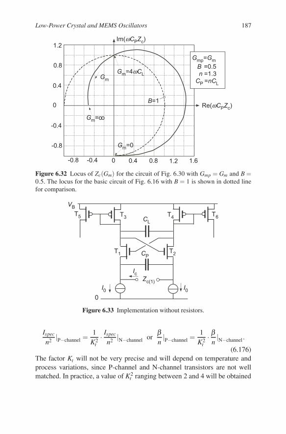
Low-Power Crystal and MEMS Oscillators 187
& &, & &+
&
&,
&
&
ω
!ω
#
#ω7
&,
/#
&
&,
#
#
/#&')#&#)7
Figure 6.32 Locus of Zc(Gm) for the circuit of Fig. 6.30 with Gmp = Gm and B =0.5. The locus for the basic circuit of Fig. 6.16 with B = 1 is shown in dotted linefor comparison.
7
> >
> >
<
>' >+
Figure 6.33 Implementation without resistors.
Ispec
n2 |P−channel =1
K2t· Ispec
n2 |N−channel orβn|P−channel =
1K2
t· β
n|N−channel.
(6.176)The factor Kt will not be very precise and will depend on temperature andprocess variations, since P-channel and N-channel transistors are not wellmatched. In practice, a value of K2
t ranging between 2 and 4 will be obtained

188 6 Alternative Architectures
for identical dimensions of N-channel and P-channel devices, due to the dif-ference of mobility between electrons and holes.
With this scheme, the original load resistance RL/2 is replaced by Kt/Gm
thus, according to (6.108):
B =2KtωCL
Gm=
2Kt
A, (6.177)
which, introduced in (6.106) and (6.107) gives
Re(Zc) =1
ωCP· 2Kt(4Kt/A + A/Kt −A)
4+(4Kt/A−A)2 (6.178)
Im(Zc) =1
ωCP· 4(2Kt −4K2
t /A2 −1)4+(4Kt/A−A)2 , (6.179)
with the normalized transconductance A defined by (6.108). The locus ofZc(Gm) is plotted in Fig. 6.34(a) for several values of the transconductanceratio Kt . It is again a spiral, but |Zc| tend to zero when Gm tends to infinity.
+#&
&'
&
&'
&
#
#
!
ω
+ ,
)& )
ω
ω!
ω
+#7#%)
Figure 6.34 (a) Locus of Zc(Gm) for the circuit of Fig. 6.33 for several values ofKt = Gm/Gmp. The locus for the circuit of Fig. 6.30 with Gmp = Gm and B = 0.5 isshown in dotted line for comparison. (b) Real and imaginary parts of Zc for Kt = 2.
No negative resistance is possible for Kt ≤ 1. The slope at Re(Zc = 0) isfurther worsened, as indicated by the comparison with the locus of Fig. 6.32,repeated here in dotted line.

Low-Power Crystal and MEMS Oscillators 189
Part (b) of the figure shows the variations of the real and imaginary partsof the circuit impedance with the transconductance, for Kt = 2. Comparedto Fig. 6.20(b) for the basic circuit, the maximum of negative resistance isalready reached for a small excess of transconductance Gm/Gmlim, and theimaginary part is strongly dependent of Gm.
Using (6.178), the limit transconductance for a negative resistance (i.e. forRe(Zc) = 0 is
Gmlim =2Kt√Kt −1
· ωCP
n. (6.180)
As shown in the plot of Fig. 6.35, it has a minimum at Kt = 2. It increasesrapidly below Kt = 1.5 but only slowly above its minimum.
'
+
,
)& &
ω7
) (% ( +
7#%)
Figure 6.35 Variation of the limit transconductance with the transconductance ratioKt .
The imaginary part of the circuit impedance for Gm = Gmlim is obtainedby introducing (6.177) and (6.180) in (6.110)
Im(Zc)lim = Im(Zc)|Re(Zc)=0 =Kt −1ωCP
. (6.181)
This can be verified in Fig. 6.34.Nonlinear effects in the modified circuits are difficult to express analyt-
ically, since the active devices and their loads are both nonlinear. Results ofa simulation of the transistors-only circuit of Fig. 6.33 for Re(Zc(1)) = 0 areplotted in Fig. 6.36.
As could be expected from the shape of the impedance locus, Im(Zc(1) =|Zc(1)| (since Re(Zc(1)=0) is very dependent on the bias current: nonlinearitieshave a much larger effect on the frequency of oscillation than in the basiccircuit (see Fig. 6.24).

190 6 Alternative Architectures
+ , &
&
&
&+
&,
&
) %
5 5
5 5
5 5
+#&L
#
Figure 6.36 Measurements of Zc(1)(I0) and |Ic|/I0 in a simulation of the modifiedcircuit of Fig. 6.33 for Re(Zc(1))=0 with Kt = 2.2.
6.4 Van den Homberg Oscillator
6.4.1 Principle and Linear Analysis
A good example of an oscillator based on an operational transconductanceamplifier (OTA) is illustrated in Fig. 6.37 [27]. The main purpose of this
I>4
+*
Figure 6.37 Principle of the oscillator proposed by van den Homberg.
structure is to provide a single pin oscillator (one side of the quartz groun-ded) with grounded capacitors only. The input Vin of the OTA is the dif-ference of voltages across the two capacitors Ca (that include the electricalcapacitor C0 of the resonator defined by (2.1)) and Cb. It delivers two separ-ate output currents. The first one is proportional to Vin by a transconductance

Low-Power Crystal and MEMS Oscillators 191
Gm and produces a positive feedback. The second one, with a proportionaltransconductance KgGm creates a negative feedback.
Assuming an ideal OTA and replacing the capacitances by more generalimpedances Za and Zb including possible losses, the small-signal circuit im-pedance is
Zc =Za + KgGmZaZb
1+ Gm(KgZb −Za), (6.182)
which is again a bilinear function of the transconductance Gm. The locus ofZc(Gm) is thus once more a circle. Without the motional impedance Zm, thecircuit must be stable, hence the real part of the poles of Zc must be negative.
With lossless capacitors, the condition for stability becomes
Cb < KgCa, (6.183)
meaning that the negative feedback gain KgGm/(ωCb) must be larger thanthe positive feedback gain Gm/(ωCa). The circular locus is centered on theimaginary axis as depicted in Fig. 6.38.
ω
ω%+*
55"
#
#
@ A
!
Figure 6.38 Locus of the circuit impedance for the oscillator of Fig. 6.37 with anideal OTA and lossless capacitors.
The real part of Zc is
Re(Zc) =−Gm
(ωCa)2 + G2m(KgCa/Cb −1)2 , (6.184)
and provides a maximum value of negative resistance
|Rn0|max =1
2ωCa(KgCa/Cb −1)for Gm = Gmopt =
ωCa
KgCa/Cb −1, (6.185)

192 6 Alternative Architectures
with Ca ≥CP.For Rm |Rn0|max (margin factor Km 1), the frequency pulling at the
critical condition for oscillation is simply, from (4.3)
pc∼= Cm
2Ca, (6.186)
and the term in G2m in the denominator of (6.184) can be neglected. Thus,
from (3.9), the critical transconductance for the lossless circuit can be ap-proximated by
Gmcrit0∼= ω2C2
aRm =ωC2
a
QCm=
ωCm
4Qp2c
(6.187)
The locus of Zc(Gm) resembles that for the Pierce oscillator depicted inFig. 4.6. Here, Ca plays the role of C3 +Cs and C3 is replaced by Ca−Cb/Kg.The latter could in principle be made as large as wanted, thereby increas-ing the value of |Rn0|max. In practice, it is limited by the need to satisfy thestability condition (6.183) in the worst case of mismatch, as for the parallelresonance oscillator of Section 6.2.
Using (6.16), the maximum value of negative resistance is therefore in therange
1− εmax
4ωCa · εmax≤ |Rn0|max ≤ ∞, (6.188)
where ε is given by (6.15) with nCD/CS replaced by KgCa/Cb.Since Ca in this circuit includes not only the electrical capacitor C0 of
the resonator, but also the overall interconnection capacitance to ground, agood matching with Cb cannot be ensured. Furthermore, since the transcon-ductance ratio Kg must be obtained by a ratio of drain currents, it will beaffected by a random error that increases when the inversion decreases. Forthese reasons, the practical value of |Rn0|max is not larger than for the basicPierce oscillator.
The comparison of (6.187) with (4.26) shows that the critical transcon-ductance for a given amount of frequency pulling pc is four times smallerthan for the Pierce oscillator. But this does not necessarily result in a re-duction of power consumption, since the OTA consumes much more currentthan a single transistor to produce the same transconductance.
At the critical condition for oscillation, the transconductance is given by(6.187) and the voltages across the capacitors are related to the differentialinput voltage of the OTA by
Vb = − jKgCa
Cb· Ca
QCmVin and Va = Vb +Vin. (6.189)

Low-Power Crystal and MEMS Oscillators 193
The value of KgCa/Cb is not much larger than unity to maximize the radiusof the circular locus of Fig. 6.38. The value of Vb/Vin therefore dependsessentially on QCm/Ca = 2Qpc. This value is often much larger than unity,resulting in |Vb| |Vin| and |Va| ∼= |Vin|.
6.4.2 Practical Implementation and Nonlinear Behavior
A full circuit implementation of the principle explained by Fig. 6.37 is shownin Fig. 6.39 [27]. The two feedback loops are implemented by adequate com-
ββ
β β
+*β
β
β+*β
<
Figure 6.39 Circuit implementation of the oscillator of Fig. 6.37.
binations of P-channel and N-channel current mirrors. The DC bias currentof each branch is I0, except in the output stage driving Cb where it is KgI0.Thus, the total current is (4+Kg)I0, plus the current flowing through the biasresistors R1 and R2. The ratio of these resistances is chosen for best centeringof the output oscillatory signal, and their value must be sufficiently large tominimize the loss conductance Ga across Ca.
Some power could be saved by reducing the bias current in some branches.But this would increase the noise excess factor γ defined in Section 3.7 andthe phase noise would be increased.
When the oscillation grows, the amplitude is limited by the nonlinear be-havior of the input differential pair. Thus its dependency on the bias currentI0 is given by (6.33) if the pair is in weak inversion, or by (6.39) if it is instrong inversion. These results are plotted in Fig. 6.6.
As for the other oscillator schemes, the bias current may be adjusted tothe desired amplitude by means of a regulating loop.
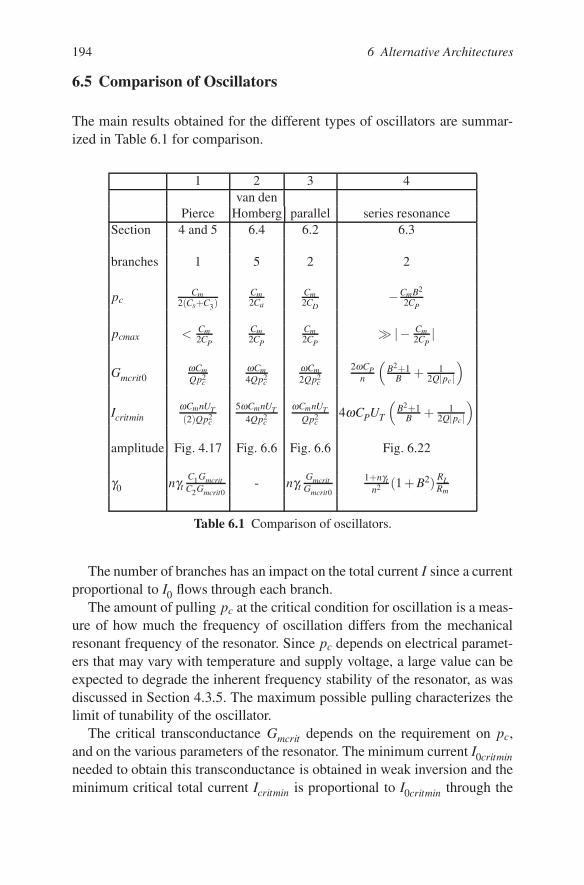
194 6 Alternative Architectures
6.5 Comparison of Oscillators
The main results obtained for the different types of oscillators are summar-ized in Table 6.1 for comparison.
1 2 3 4van den
Pierce Homberg parallel series resonanceSection 4 and 5 6.4 6.2 6.3
branches 1 5 2 2
pcCm
2(Cs+C3)Cm2Ca
Cm2CD
−CmB2
2CP
pcmax < Cm2CP
Cm2CP
Cm2CP
|− Cm2CP
|
Gmcrit0ωCmQp2
c
ωCm4Qp2
c
ωCm2Qp2
c
2ωCPn
(B2+1
B + 12Q|pc|
)
IcritminωCmnUT(2)Qp2
c
5ωCmnUT4Qp2
c
ωCmnUTQp2
c4ωCPUT
(B2+1
B + 12Q|pc|
)
amplitude Fig. 4.17 Fig. 6.6 Fig. 6.6 Fig. 6.22
γ0 nγtC1GmcritC2Gmcrit0
- nγtGmcritGmcrit0
1+nγtn2 (1 + B2) RL
Rm
Table 6.1 Comparison of oscillators.
The number of branches has an impact on the total current I since a currentproportional to I0 flows through each branch.
The amount of pulling pc at the critical condition for oscillation is a meas-ure of how much the frequency of oscillation differs from the mechanicalresonant frequency of the resonator. Since pc depends on electrical paramet-ers that may vary with temperature and supply voltage, a large value can beexpected to degrade the inherent frequency stability of the resonator, as wasdiscussed in Section 4.3.5. The maximum possible pulling characterizes thelimit of tunability of the oscillator.
The critical transconductance Gmcrit depends on the requirement on pc,and on the various parameters of the resonator. The minimum current I0critminneeded to obtain this transconductance is obtained in weak inversion and theminimum critical total current Icritmin is proportional to I0critmin through the

Low-Power Crystal and MEMS Oscillators 195
number of branches. Somewhat larger values are needed to obtain a usableamplitude.
Calculations have shown that the phase noise excess factor γ does notchange very much with the amplitude of oscillation. Its value γ0 at smallamplitude is therefore used in the comparison. The effect of the noise comingfrom the bias current is not included.
6.5.1 Pierce Oscillator (1)
It is the most simple structure since the basic circuit (Fig. 4.1) requires asingle active transistor. The current can be minimized by using the current-controlled CMOS implementation of Fig. 5.25, but the simple implement-ation with a CMOS inverter (Fig. 5.21) has many drawback, and shouldbe avoided. The two functional capacitors C1 and C2 are grounded in thegrounded source implementations (Fig. 5.1 ), but the resonator is not. Theresonator may be grounded by using the grounded-drain implementation(Fig. 5.27), but C1 is then floating.
Oscillation is only possible if the total impedance Z3 + Zm between gateand drain is inductive. Therefore, according to the condition (4.16), the fig-ure of merit M defined by (2.9) must be larger than 2. This condition shouldbe satisfied with a large margin to maximize the frequency stability, but thismargin is reduced in the grounded-drain implementation. The motional im-pedance Zm is also inductive at stable oscillation, thus the pulling pc givenby (4.21) is always positive. It may be reduced by increasing Cs, the seriesconnection of the two functional capacitors C1 and C2. The maximum pullingis limited by CP, the electrical capacitance C0 of the resonator augmented byunavoidable parasitic capacitors.
The critical transconductance of the lossless circuit Gmcrit0 is related to pc
by (4.26) and is minimum for C1 = C2. The minimum critical total current issimply nUT Gmcrit0. It may be reduced by a factor 2 by replacing the singletransistor by a complementary pair.
The amplitude of oscillation depends on I0/I0critmin according to Fig. 4.17.A current I ≥ 2.8Icritmin is needed to obtain an amplitude |V1| = 5nUT at thegate.
The noise excess factor γ0 is minimum for C1 = C2. It increases with theincrease of critical transconductance Gmcrit/Gmcrit0 due to lossy components,but the noise associated with these components is not included.

196 6 Alternative Architectures
6.5.2 Van den Homberg Oscillator (2)
This is the most complicated of the 4 schemes, since it requires a fulldouble output operational transconductance amplifier (OTA), as illustratedin Fig. 6.37. Thus a minimum of 5 branches are needed with at least 5 in-ternal nodes (Fig. 6.39). The poles related to these internal nodes should bemade negligible, as was implicitly assumed in the analysis. The two func-tional capacitors Ca and Cb are grounded, as well as the resonator that isused as a dipole.
This circuit has no requirement on a minimum value of the figure of merit,but the condition for stability (6.183) must be fulfilled so that the negativefeedback through Cb overrides the positive feedback through Ca. The circuitimpedance Zc is therefore always capacitive and thus the pulling pc givenby (6.186) always positive. It can be reduced by increasing Ca. Its maximumvalue pcmax is obtained for Ca = CP.
The minimum critical transconductance for a given value of pc is close toone fourth of that of the Pierce circuit. However, the total critical current isabout the same as the non-complementary implementation if the currents inthe 5 branches are equal, as it should be to avoid increasing the noise.
The amplitude of oscillation is limited by the transfer function of the dif-ferential pair. Its dependency on I/Icritmin is plotted in Fig. 6.6. A currentI ≥ 2.5Icritmin is needed to obtain an amplitude |Vin| = 5nUT at the input ofthe OTA. According to (6.189), the amplitude |Va| across the resonator isalways larger or equal to |Vin|.
The phase noise has not been evaluated for this oscillator, but its is expec-ted to be increased by the larger number of active components.
6.5.3 Parallel Resonance Oscillator (3)
This is a symmetrical circuit which delivers complementary output voltagesat the drain of the two transistors (Fig. 6.1(b)). It emulates a parallel resonatorby using the parallel resonance of the motional impedance Zm combinedwith the parallel capacitor CP. The latter can be increased to a value CDby an additional capacitor to reduce the pulling. This additional capacitorcan be connected across the resonator, or it can be split in two groundedcapacitor of double value. The sources of the transistor must be AC coupledby a capacitor CS to avoid DC bistability. This capacitor can also be replacedby two grounded capacitors of value 2CS.

Low-Power Crystal and MEMS Oscillators 197
There is no condition on the maximum value of CD (and thus on the min-imum value of the figure of merit ML defined by (6.7)). But to ensure ACstability at other frequencies then that of the resonator, the maximum valueof CS is limited by the condition (6.6). The impedance Zc of the stable circuitis always capacitive, thus the pulling pc given by (6.17) is always positive.Its minimum value is obtained when CD is limited to CP ≥C0.
The minimum critical transconductance for the lossless circuit Gmcrit0 ishalf that of the Pierce oscillator, but the minimum critical current Icritmin isthe same, since the bias current flows in 2 branches.
As long as the impedance of the capacitance CS is negligible comparedto their source transconductance (condition (6.28) fulfilled), the active tran-sistors operate as a differential pair. The variation of the drain to drain (orgate to gate) voltage amplitude |Vin| with I/Icritmin is shown in Fig. 6.6 forweak inversion, and for strong inversion with a given value of inversion coef-ficient IC = I0/Ispec (thus not for a fixed value of specific current Ispec of thetransistors).
The small-amplitude noise excess factor γ0 is the same as that of the Pierceoscillator with C1 = C2.
6.5.4 Series Resonance Oscillator (4)
Whereas the first three oscillators above have comparable characteristics inspite of their different architectures, the series resonance oscillator depictedin Fig. 6.16 is very different in many aspects.
The function of the active devices of this symmetrical circuit is to changethe sign of the load resistor RL to obtain a negative resistance. Because of thecapacitance CP across the motional impedance Zm of the resonator, a load ca-pacitance CL is needed to avoid parasitic oscillations. It must be sufficientlylarge to fulfill the condition (6.104), but not too large, since it would reducethe negative resistance. To simplify the analysis, all the derivations havebeen carried out with the assumption that the sufficient condition (6.103)is just fulfilled, i.e. CL = CP/n. The circuit impedance is always inductive(Re(Zc > 0), thus the pulling pc is always negative; the frequency of oscilla-tion is lower than the mechanical resonance frequency of the resonator. Thepulling depends on the value of the load resistor RL. But this load resist-ance is neither precise nor constant in an integrated circuit. The value of |pc|increases with B2, and its maximum is not limited.
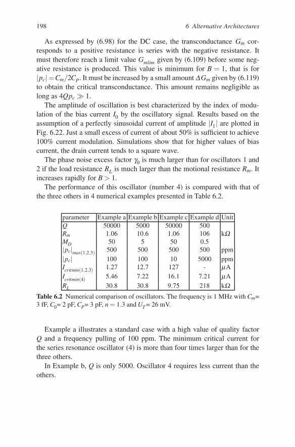
198 6 Alternative Architectures
As expressed by (6.98) for the DC case, the transconductance Gm cor-responds to a positive resistance is series with the negative resistance. Itmust therefore reach a limit value Gmlim given by (6.109) before some neg-ative resistance is produced. This value is minimum for B = 1, that is for|pc|=Cm/2CP. It must be increased by a small amount ∆Gm given by (6.119)to obtain the critical transconductance. This amount remains negligible aslong as 4Qpc 1.
The amplitude of oscillation is best characterized by the index of modu-lation of the bias current I0 by the oscillatory signal. Results based on theassumption of a perfectly sinusoidal current of amplitude |I1| are plotted inFig. 6.22. Just a small excess of current of about 50% is sufficient to achieve100% current modulation. Simulations show that for higher values of biascurrent, the drain current tends to a square wave.
The phase noise excess factor γ0 is much larger than for oscillators 1 and2 if the load resistance RL is much larger than the motional resistance Rm. Itincreases rapidly for B > 1.
The performance of this oscillator (number 4) is compared with that ofthe three others in 4 numerical examples presented in Table 6.2.
parameter Example a Example b Example c Example d UnitQ 50000 5000 50000 500Rm 1.06 10.6 1.06 106 kΩMD 50 5 50 0.5|pc|max(1,2,3) 500 500 500 500 ppm
|pc| 100 100 10 5000 ppmIcritmin(1,2,3) 1.27 12.7 127 - µAIcritmin(4) 5.46 7.22 16.1 7.21 µA
RL 30.8 30.8 9.75 218 kΩTable 6.2 Numerical comparison of oscillators. The frequency is 1 MHz with Cm=3 fF, C0= 2 pF, CP= 3 pF, n = 1.3 and UT = 26 mV.
Example a illustrates a standard case with a high value of quality factorQ and a frequency pulling of 100 ppm. The minimum critical current forthe series resonance oscillator (4) is more than four times larger than for thethree others.
In Example b, Q is only 5000. Oscillator 4 requires less current than theothers.
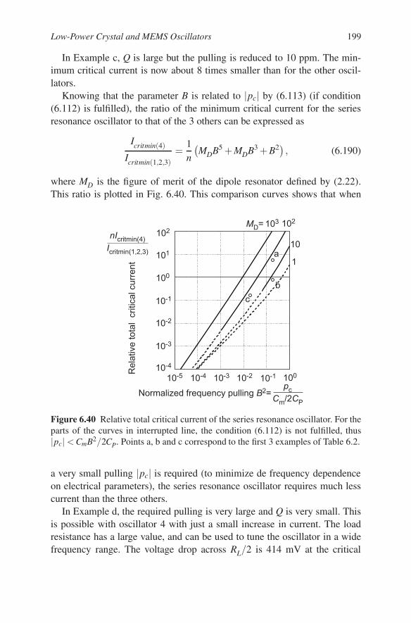
Low-Power Crystal and MEMS Oscillators 199
In Example c, Q is large but the pulling is reduced to 10 ppm. The min-imum critical current is now about 8 times smaller than for the other oscil-lators.
Knowing that the parameter B is related to |pc| by (6.113) (if condition(6.112) is fulfilled), the ratio of the minimum critical current for the seriesresonance oscillator to that of the 3 others can be expressed as
Icritmin(4)
Icritmin(1,2,3)=
1n
(MDB5 + MDB3 + B2) , (6.190)
where MD is the figure of merit of the dipole resonator defined by (2.22).This ratio is plotted in Fig. 6.40. This comparison curves shows that when
'
) B*/#
%
)
;#
Figure 6.40 Relative total critical current of the series resonance oscillator. For theparts of the curves in interrupted line, the condition (6.112) is not fulfilled, thus|pc| < CmB2/2CP. Points a, b and c correspond to the first 3 examples of Table 6.2.
a very small pulling |pc| is required (to minimize de frequency dependenceon electrical parameters), the series resonance oscillator requires much lesscurrent than the three others.
In Example d, the required pulling is very large and Q is very small. Thisis possible with oscillator 4 with just a small increase in current. The loadresistance has a large value, and can be used to tune the oscillator in a widefrequency range. The voltage drop across RL/2 is 414 mV at the critical

200 6 Alternative Architectures
current, so about 600 mV for full current modulation; this is still compatiblewith low supply voltage.
The series resonance oscillator is thus interesting for its large tuning rangecapability, for minimizing the current when a very low value of pulling isrequired, and/or for low-Q resonators.

Bibliography
1. W. G. Cady. “Method of Maintaining Electric Currents of Constant Frequency”,US patent 1,472,583, filed May 28, 1921, issued Oct. 30, 1923.
2. G. W. Pierce, “Piezoelectric Crystal Resonators and Crystal Oscillators Appliedto the Precise Calibration of Wavemeters”, Proc. American Academy of Artsand Sciences, vol. 59, October 1923, pp. 81-106.
3. G. W. Pierce, “Electrical System”, US patent 2,133,642, filed Febr. 25, 1924 ,issued Oct. 18, 1938.
4. W. A. Marrison and J.W. Horton, ”Precision Determination of Frequency”.I.R.E. Proc. vol. 16, pp. 137154 Feb., 1928.
5. E. Vittoz, The Electronic Watch and Low-Power Circuits”, IEEE Solid-StateCircuits Society News, Vol. 13, No. 3, Summer 2008, pp.7-23.
6. A. Hadjimiri and T. H. Lee, “A General Theory of Phase Noise in ElectricalOscillators”, IEEE J. Solid-State Circuits, vol. 33, pp. 179-194, Febr. 1998.Corrections at page 928 of the same journal (June 1998).
7. V. Uzunoglu, Semiconductor Network Analysis and Design, McGraw Hill,1964, p.245.
8. M.R. Spiegel, Complex Variables, Schaum Publishing Co, New York, 1964.
9. F.E. Terman, Radio Engineering HandBook, McGraw-Hill, 1943.
10. E. Momosaki, ”A Brief Review of Progress in Quartz Tuning Fork Resonators”,Proceedings of the 1997 IEEE International Frequency Control Symposium,1997, pp. 552-565, 28-30 May 1997.
11. W. P. Mason, “A New Quartz Crystal Plate, Designated the GT, Which Producesa Very Constant Frequency Over a Wide Temperature Range”, Proc. IRE, vol.28, p. 220, May 1940.
201

202 Bibliography
12. J. Hermann,”A Novel Miniature ZT-Cut Resonator”, Proc. of the 39th AnnualSymposium on Frequency Control, 1085, pp. 375-380.
13. E. Vittoz, ”Quartz Oscillators for Watches”, invited paper, Proc. 10th Interna-tional Congress of Chronometry, pp. 131-140, Geneva, 1979.
14. E. Vittoz, M. Degrauwe and S. Bitz, ”High-Performance Crystal Oscillator Cir-cuits: Theory and Applications”, IEEE J. Solid-State Circuits, vol. SC-23, pp.774-783, June 1988.
15. H. J. Reich, Functional Circuits and Oscillators, Boston technical Publishers,Cambridge MS, 1965.
16. D. B. Leeson, “A Simple Model of Feedback Oscillator Noise Spectrum”, Proc.IEEE, Vol. 54, pp. 329-330, Febr. 1966.
17. C. Enz, F. Krummenacher and E. Vittoz, “An Analytical MOS Transistor ModelValid in All Regions of Operation and Dedicated to Low-Voltage and Low-Current Applications”, Analog Integrated Circuits and Signal Processing, Vol.8,pp. 83-114, 1995.
18. C. Enz and E. Vittoz, Charge-Based MOS Transistor Modeling, John Wiley andSons, Chichester, 2006.
19. H. Oguey and S. Cserveny, “MOS Modelling at Low Current Density”, SummerCourse on Process and Device Modelling. ESAT-Leuven, June 1983.
20. J. K. Clapp, “An inductive-Capacitive Oscillator of Unusual Frequency Stabil-ity”, Proc. IRE, vol. 36, 1948, pp. 356-358.
21. E. Vittoz and J. Fellrath, ”CMOS Analog Integrated Circuits Based on WeakInversion Operation”, IEEE J. Solid-State Circuits, vol. SC-12, pp. 224-231,June 1977.
22. D. A. Aebischer, H. J. Oguey and V. R. von Kaenel, “A 2.1MHz Crystal Os-cillator Time Base With a Current Consumption under 500nA”, IEEE J. Solid-State Circuits, vol. 32, pp. 999-1005, July 1997.
23. J.Santos and R. Meyer, “A One-Pin Oscillator for VLSI Circuits”, IEEE J.Solid-State Circuits, vol. SC-19, pp. 228-236, April 1984.
24. J. Luescher, “Oscillator Circuit Including a Quartz Crystal Operating in ParallelResonance”, US patent 3,585,527, filed oct. 27, 1969, issued June 15, 1971.
25. D. Ruffieux, “A High-Stability, Ultra-Low-Power Differential Oscillator Circuitfor Demanding Radio Applications”, Proc. ESSCIRC’02, pp. 85-88, 2002.
26. M. P. Forrer, “Survey of Circuitry for Watches”, Proc. IEEE, vol. 60, pp.1047-1054, Sept. 1972.
27. J.A.T.M. van den Homberg, “A Universal 0.03-mm2 One-Pin Crystal Oscillatorin CMOS”, IEEE J. Solid-State Circuits, vol. 34, pp. 956-961, July 1999.

Index
amplitudedetector, 73increase of, 62, 106limitation, 27, 28, 58of drain voltage, 94, 184of gate voltage, 58, 61, 62, 65of oscillation, 5, 61, 62, 65, 94, 146,
162regulation, 73, 107, 122, 162
stability, 116, 117regulator, 108
curve, 110, 121, 163simplified, 117
stability, 5
bias current, 61, 145critical, 61, 64, 108, 161start-up, 109
bilinear function, 11, 43, 167
capacitancegate oxide, 37load, 48motional, 8parallel, 8, 14parasitic, 8
capacitiveattenuator, 62circuit impedance, 196coupling, 22, 138load, 123
transducer, 18channel length modulation, 39
voltage, 39channel noise excess factor, 40circuit impedance, 24, 43, 70, 165, 166,
191for the fundamental, 24, 31, 55, 69
locus of, 24, 26, 56, 125locus of, 43, 46, 52, 56, 134, 141,
158, 160, 162, 167, 170, 172,187, 188, 191
real and imaginary parts, 167, 170,172
couplingcoefficient, 9, 18electromechanical, 9factor, 14, 18, 21
criticalcondition for oscillation, 27, 43current, 108, 126, 161
minimum, 61, 64, 147, 194supply voltage, 125, 126transconductance, 44, 49, 59, 139,
143, 169, 170, 194current
bias, 65specific, 37, 162
cyclostationary noise, 33, 79, 81, 149,151, 154, 157, 177, 179, 181
design
203

204 Index
example, 89, 100, 117process, 84
differential pair, 137distortion
of drain current, 174of gate voltage, 57
drain current, 36forward component of, 36reverse component of, 36
duality, 30dynamic behavior
of bias, 95, 97of oscillation amplitude, 97, 100
electromechanicalcoupling, 9transducing property, 16
electrostatic transducer, 18energy
dissipation, 34exchange of, 24, 34kinetic, 15mechanical, 7, 15, 68, 148of oscillation, 33potential, 15thermal, 30
equivalent circuitof series resonance oscillator, 164
for small signal, 164of parallel resonance oscillator, 140
for small signal, 140of Pierce oscillator, 42
for small signal, 42of quartz resonator, 8, 10
figure of merit, 18–20, 22, 47of dipole resonator, 14of loaded dipole resonator, 139of resonator, 10, 14
frequencyadjustment, 54parallel resonance, 11–13pulling, 10resonant, 8, 16, 138series resonance, 11–13
stability, 69frequency pulling, 54, 139
at critical condition, 27, 44, 48, 142,168, 171, 194
at stable oscillation, 26, 57effect of losses on, 53
fundamental componentof control voltage, 173, 174of drain current, 59, 60, 63of output current, 146, 147of voltage, 24, 55
impedancemotional, 8, 10parallel, 11, 139
locus of, 11, 139impulse sensitivity function (ISF), 33,
34, 79, 81–83, 152, 153, 180, 182inversion
coefficient, 37at bias current, 146at critical current, 63, 174
strong, 37, 38weak, 37, 38
linearanalysis, 42, 55, 139, 144, 165, 172,
190, 193approximation, 27circuit, 27
noise, 31, 33, 150, 178function, 103impedance, 10range of operation, 27resistive element, 102
loadcapacitance, 48resistance, 188resistor, 165
losses, 43, 163effect of, 52, 54, 75, 143
on frequency pulling, 53lossless
capacitor, 46circuit, 46, 51, 55, 84, 139

Low-Power Crystal and MEMS Oscillators 205
mechanicalenergy of oscillation, 15, 68, 148power dissipation, 15, 68, 148
MEM resonators, 18, 22mode
activity, 72contour, 17flexural, 16fundamental, 10of oscillation, 7overtone, 10thickness, 17torsional, 17unwanted, 71, 128wanted, 10
modulation indexof current, 173, 174, 180of differential pair, 146of gate voltage, 81
MOS transistordrain current, 36EKV model, 36, 40, 55intrinsic voltage gain, 39saturation, 37slope factor, 37specific current, 37threshold voltage, 37, 94transfer function, 58transfer parameter, 37
motionalcapacitance, 8current, 9, 15impedance, 8, 24, 30, 41, 68
locus of, 43, 141inductance, 8resistance, 8
negative resistance, 41, 43, 44, 47, 52,56, 137
current stable, 164maximum, 47, 141, 142, 158, 160,
168, 191voltage stable, 138
noisechannel noise, 39
cyclostationary, 33, 79, 81, 149, 151,154, 157, 177, 179, 181
excess factor, 31, 77, 78, 80, 83, 151,152, 154, 195
flicker, 35, 81–83, 154, 157, 181, 183model, 40
of bias current, 83phase noise, 31, 35, 36, 77, 84, 149,
157, 177, 183thermal, 35white, 34, 35, 77–79, 81, 150, 154,
178, 180nonlinear
analysis, 55, 77, 144, 148, 172, 177effects, 25, 55, 65, 69, 176, 189
simulation of, 56, 125, 176example, 55transfer function, 58, 65
oscillationamplitude, 24, 61, 62, 65, 146critical condition for, 27, 43energy, 15, 33mode of, 8, 16
unwanted, 128parasitic, 139, 166signal extraction, 123, 185stable, 25, 26, 31, 59start-up of, 29start-up of
time constant, 29, 47oscillator
applications of, 1basics on, 4comparison of, 194, 200current-mode, 184parallel resonance, 196Pierce, 2, 41, 91, 93, 135, 195
CMOS inverter, 124, 131grounded drain, 132, 135grounded source, 93, 131
quartz, 1series resonance, 197single pin, 132, 190symmetrical

206 Index
for parallel resonance, 137, 164for series resonance, 164, 189
van den Homberg, 190, 193, 195
parallel resonance oscillator, 137, 164,196
phasenoise, 31, 34–36, 77, 84, 149, 157,
177, 183shift, 79–81, 150, 154, 180stability, 5, 31, 43, 50, 138
Pierce oscillator, 2, 41, 91, 93, 135, 195CMOS inverter, 124, 131
current-controlled, 129, 131simulation, 125
grounded drain, 132, 135grounded source, 93, 131
practical implementationof parallel resonance oscillator, 157,
164of Pierce oscillators, 93, 135of series resonance oscillator, 183,
189of van den Homberg oscillator, 193
quality factor, 8, 24, 33, 44, 46, 53, 57,70, 72, 77, 84, 89
quartzcrystal, 15production, 2
quartz resonator, 7cut
AT, 17CT, 17GT, 17
equivalent circuit, 8resonant frequency of, 8types of, 15
resistorelimination, 120implementation, 102
load, 165resonance
parallel, 11, 138series, 11
resonant circuitparallel, 30series, 8, 30
resonatordipole, 14mechanical, 7MEM, 18, 21, 22quartz, 7
saturationdrain voltage, 94of MOS transistor, 37
series resonance oscillator, 164, 189,197
strong inversion, 37, 63, 80, 82, 94,146, 152
strict, 66, 88, 94, 146
thermodynamic voltage, 37transconductance
amplifier, 190critical, 44, 49, 52, 59, 139, 143, 169,
170, 194drain transconductance, 38for the fundamental frequency, 59,
67, 146gate transconductance, 38in saturation, 39limit for negative resistance, 167, 189maximum, 49optimum, 43, 46, 169source transconductance, 38
van den Homberg oscillator, 190, 193,195
weak inversion, 37, 60, 62, 64, 72, 79,81, 86, 89, 94, 146, 151, 155