Embed Size (px)
Citation preview
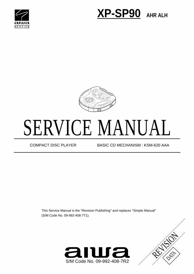
BASIC CD MECHANISM : KSM-620 AAACOMPACT DISC PLAYER
XP-SP90
S/M Code No. 09-992-408-7R2
AHR ALH
SERVICE MANUAL
REVISION
DATA
This Service Manual is the "Revision Publishing" and replaces "Simple Manual"
(S/M Code No. 09-992-408-7T1).
2
SPECIFICATIONS
• Design and specif icat ions are subject to change withoutnot ice.
REF. NO PART NO. KANRI DESCRIPTIONNO.
ACCESSORIES/PACKAGE LIST
1 8Z-HC3-914-010 IB,HR(ECA)C<AHR> 1 8Z-HC3-916-010 IB,LH(3L)C<ALH>! 2 87-042-201-110 AC ADAPTOR,AC-A62 HEJ 3 87-B30-225-010 HEADPHONE,HP-M034! 4 87-A90-312-010 PLUG,CONVERSION WTN-1157R1
3
PROTECTION OF EYES FROM LASER BEAM DURING SERVICING
VAROITUS!Laiteen Käyttäminen muulla kuin tässä käyttöohjeessa mainit-
ulla tavalla saattaa altistaa käyt-täjän turvallisuusluokan 1 ylit-
tävälle näkymättömälle lasersäteilylle.
VARNING!Om apparaten används på annat sätt än vad som specificeras i
denna bruksanvising, kan användaren utsättas för osynling
laserstrålning, som överskrider gränsen för laserklass 1.
Caution: Invisible laser radiation when
open and interlocks defeated avoid expo-
sure to beam.
Advarsel:Usynling laserståling ved åbning,
når sikkerhedsafbrydere er ude af funktion.
Undgå udsættelse for stråling.
CAUTIONUse of controls or adjustments or performance of procedures
other than those specified herein may result in hazardous
radiation exposure.
ATTENTIONL'utilisation de commandes, réglages ou procédures autres que
ceux spécifiés peut entraîner une dangereuse exposition aux
radiations.
ADVARSEL!Usynlig laserståling ved åbning, når sikkerhedsafbrydereer ude
af funktion. Undgå udsættelse for stråling.
This Compact Disc player is classified as a CLASS 1 LASER
product.
The CLASS 1 LASER PRODUCT label is located on the rear
exterior.
This set employs laser. Therefore, be sure to follow carefully the
instructions below when servicing.
WARNING!WHEN SERVICING, DO NOT APPROACH THE LASER EXIT
WITH THE EYE TOO CLOSELY. IN CASE IT IS NECESSARY TO
CONFIRM LASER BEAM EMISSION. BE SURE TO OBSERVE
FROM A DISTANCE OF MORE THAN 30cm FROM THE
SURFACE OF THE OBJECTIVE LENS ON THE OPTICAL
PICK-UP BLOCK.
CLASS 1KLASSE 1LUOKAN 1KLASS 1
LASER PRODUCTLASER PRODUKTLASER LAITELASER APPARAT
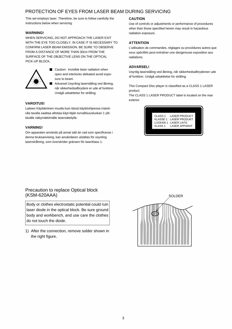
Precaution to replace Optical block(KSM-620AAA)
1) After the connection, remove solder shown inthe right figure.
Body or clothes electrostatic potential could ruinlaser diode in the optical block. Be sure groundbody and workbench, and use care the clothesdo not touch the diode.
SOLDER
4
REF. NO PART NO. KANRI DESCRIPTIONNO.
REF. NO PART NO. KANRI DESCRIPTIONNO.
ELECTRICAL MAIN PARTS LIST
IC
87-A21-082-040 C-IC,BA6655AFV 87-A21-083-040 C-IC,BH6508FS 87-A21-087-010 C-IC,CXA2542AR 87-A20-916-010 C-IC,CXD3009Q 87-A21-208-010 C-IC,HM51W17400LTS-6/7
87-A21-262-010 C-IC,SM5903AF 87-A21-085-040 C-IC,TA2120FN 8Z-HC3-620-010 C-IC,CXP83417-159Q 87-017-631-080 IC,AT93C46R
TRANSISTOR
87-A30-183-040 C-TR,2SD1628G 89-211-323-080 C-TR,2SB1132R 89-113-695-680 C-TR,2SA1369G/H 87-026-608-080 C-TR,DTC 123 JK 86-NFZ-687-080 C-TR,2SA1037S
89-416-643-080 C-TR,2SD1664R 89-324-121-080 C-TR,2SC2412K 87-026-239-080 TR,DTC114TK (0.2W) 87-026-235-080 CHIP-TR,DTC114EK 87-026-233-080 TR,DTA114TK-TP
87-026-211-080 TR,DTA144EK
DIODE
87-A40-592-040 C-ZENER,HZM11NB2 87-A40-469-040 C-DIODE,HSM2838CTR 87-A40-590-040 C-DIODE,HRW0202A
MAIN C.B
C101 87-010-561-040 CAP,E 100-16 GAS C102 87-010-502-040 CAP ELECT GAS 100/4 C103 87-010-831-080 C-CAP,U,0.1-16F C104 87-A10-505-080 CAP,E 220-6.3 SF C106 87-010-503-040 CAP,E 220-4 GAS
C107 87-010-831-080 C-CAP,U,0.1-16F C109 87-012-199-080 CAP 220P C110 87-010-502-040 CAP ELECT GAS 100/4 C111 87-A10-025-080 C-CAP,U 0.22-16Z F C112 87-012-274-080 CHIP CAP,U 1000P-50B
C113 87-010-829-080 CAP, U 0.047-16 C115 87-A10-047-080 C-CAP,U 1-10 Z F C124 87-A10-047-080 C-CAP,U 1-10 Z F C201 87-012-273-080 C-CAP,U 820P-50 B C202 87-012-287-080 C-CAP,U 0.015-25 F
C203 87-012-287-080 C-CAP,U 0.015-25 F C204 87-012-287-080 C-CAP,U 0.015-25 F C205 87-012-287-080 C-CAP,U 0.015-25 F C206 87-012-286-080 CAP, U 0.01-25 C207 87-010-502-040 CAP ELECT GAS 100/4
C208 87-A10-047-080 C-CAP,U 1-10 Z F C209 87-010-831-080 C-CAP,U,0.1-16F C210 87-A10-047-080 C-CAP,U 1-10 Z F C211 87-A10-463-080 C-CAP,U 0.47-10 Z F C301 87-012-274-080 CHIP CAP,U 1000P-50B
C302 87-A11-066-080 C-CAP,TN 47-4 M TCMS-B2R C303 87-012-274-080 CHIP CAP,U 1000P-50B C304 87-010-831-080 C-CAP,U 0.1-16 Z F C305 87-010-831-080 C-CAP,U 0.1-16 Z F C306 87-010-831-080 C-CAP,U 0.1-16 Z F
C307 87-012-199-080 C-CAP,U 220P-50 J CH C308 87-010-421-040 CAP,E 4.7-50 5L C311 87-010-788-080 C-CAP,U 0.033-2.5F C312 87-012-286-080 C-CAP,U 0.01-25 K B C313 87-012-195-080 C-CAP,U 100P-50CH
C314 87-A10-047-080 C-CAP,U 1-10 Z F
C315 87-010-498-040 CAP,E 10-16 GAS C316 87-012-278-080 C-CAP,U 2200P-50 B C317 87-010-502-040 CAP ELECT GAS 100/4 C318 87-010-502-040 CAP ELECT GAS 100/4 C319 87-010-788-080 C-CAP,U 0.033-2.5F
C320 87-012-286-080 CAP, U 0.01-25 C321 87-012-286-080 CAP, U 0.01-25 C322 87-010-788-080 C-CAP,U 0.033-2.5F C323 87-012-172-080 CAPACITOR CHIP U 10P CH C324 87-010-787-080 CAP, U 0.022-25
C325 87-010-831-080 C-CAP,U 0.1-16 Z F C326 87-012-286-080 CAP, U 0.01-25 C327 87-A11-066-080 C-CAP,TN 47-4 M TCMS-B2R C328 87-A11-066-080 C-CAP,TN 47-4 M TCMS-B2R C329 87-010-959-080 CHIP CAP,U 0.056-16F
C331 87-010-829-080 CAP, U 0.047-16 C332 87-010-829-080 CAP, U 0.047-16 C333 87-A10-047-080 C-CAP,U 1-10 Z F C334 87-010-502-040 CAP ELECT GAS 100/4 C335 87-012-165-080 CAP 3P
C336 87-A10-047-080 C-CAP,U 1-10 Z F C350 87-010-829-080 CAP, U 0.047-16 C351 87-012-280-080 CAP, U 3300P-50 C352 87-012-279-080 C-CAP,U 2700P-50 B C353 87-012-199-080 CAP 220P
C354 87-A10-463-080 C-CAP,U 0.47-10 Z F C355 87-010-831-080 C-CAP,U 0.1-16 Z F C356 87-010-503-040 CAP,E 220-4 GAS C357 87-012-188-080 C-CAP,U 47P-50 CH C358 87-010-503-040 CAP,E 220-4 GAS
C359 87-010-831-080 C-CAP,U,0.1-16F C360 87-A10-463-080 C-CAP,U 0.47-10 Z F C362 87-012-178-080 C-CAP,U 18P-50 CH C364 87-010-831-080 C-CAP,U,0.1-16F C365 87-010-831-080 C-CAP,U,0.1-16F
C366 87-A11-066-080 C-CAP,TN 47-4 M TCMS-B2R C371 87-012-277-080 C-CAP, U 1800P-50 B C372 87-012-277-080 C-CAP, U 1800P-50 B C373 87-012-269-080 C-CAP,U 390P-50 B C374 87-012-269-080 C-CAP,U 390P-50 B
C375 87-012-274-080 CHIP CAP,U 1000P-50B C376 87-010-831-080 C-CAP,U,0.1-16F C401 87-012-274-080 CHIP CAP,U 1000P-50B C402 87-010-502-040 CAP ELECT GAS 100/4 C403 87-010-831-080 C-CAP,U,0.1-16F
C405 87-012-188-080 C-CAP,U 47P-50 CH C701 87-A10-047-080 C-CAP,U 1-10 Z F C702 87-A10-047-080 C-CAP,U 1-10 Z F C703 87-010-831-080 C-CAP,U,0.1-16F C704 87-010-831-080 C-CAP,U,0.1-16F
C705 87-010-503-040 CAP,E 220-4 GAS C706 87-010-503-040 CAP,E 220-4 GAS C707 87-012-274-080 CHIP CAP,U 1000P-50B C708 87-012-274-080 CHIP CAP,U 1000P-50B C751 87-A11-065-080 C-CAP,TN 10-4 M TCMS-AR
C752 87-A11-065-080 C-CAP,TN 10-4 M TCMS-AR C753 87-A10-047-080 C-CAP,U 1-10 Z F C754 87-A11-065-080 C-CAP,TN 10-4 M TCMS-AR C756 87-010-502-040 CAP ELECT GAS 100/4 C801 87-010-502-040 CAP ELECT GAS 100/4
C802 87-010-831-080 C-CAP,U,0.1-16F C804 87-012-274-080 CHIP CAP,U 1000P-50B C805 87-012-199-080 CAP 220P C806 87-010-831-080 C-CAP,U,0.1-16F C807 87-012-188-080 C-CAP,U 47P-50 CH
C808 87-012-188-080 C-CAP,U 47P-50 CH C813 87-012-274-080 CHIP CAP,U 1000P-50B C837 87-A10-047-080 C-CAP,U 1-10 Z F CN201 87-A60-757-080 C-CONN,16P H IL-402R-16S CN202 87-009-411-010 CONN,6P ZH V
65
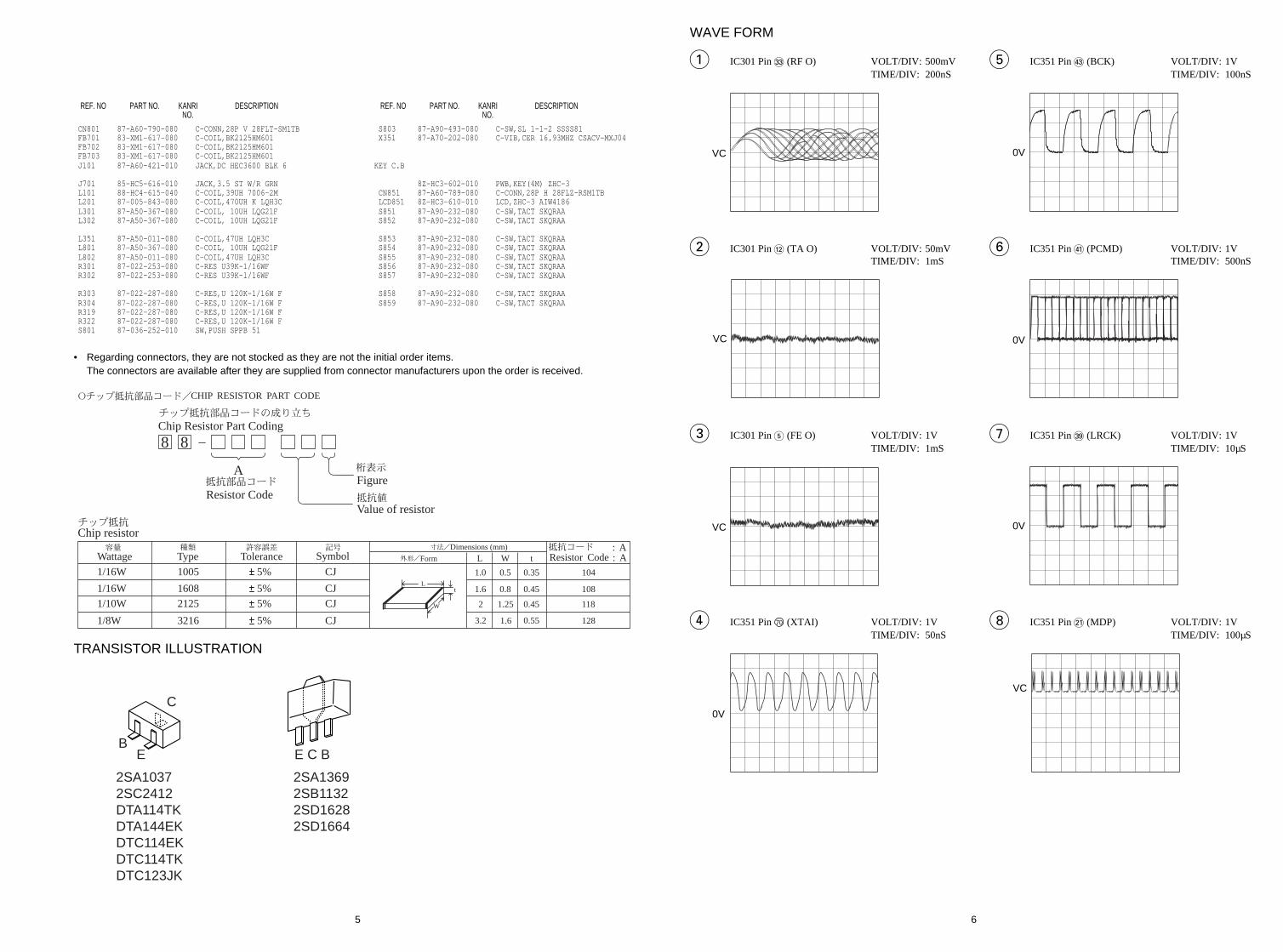
WAVE FORM
1 IC301 Pin ‹ (RF O) VOLT/DIV: 500mVTIME/DIV: 200nS
VC
2 IC301 Pin @ (TA O) VOLT/DIV: 50mVTIME/DIV: 1mS
VC
3 IC301 Pin 5 (FE O) VOLT/DIV: 1VTIME/DIV: 1mS
VC
4 IC351 Pin (XTAI) VOLT/DIV: 1VTIME/DIV: 50nS
0V
5 IC351 Pin , (BCK) VOLT/DIV: 1VTIME/DIV: 100nS
0V
6 IC351 Pin = (PCMD) VOLT/DIV: 1VTIME/DIV: 500nS
0V
7 IC351 Pin · (LRCK) VOLT/DIV: 1VTIME/DIV: 10µS
0V
8 IC351 Pin ¡ (MDP) VOLT/DIV: 1VTIME/DIV: 100µS
VC
70
REF. NO PART NO. KANRI DESCRIPTIONNO.
REF. NO PART NO. KANRI DESCRIPTIONNO.
TRANSISTOR ILLUSTRATION
8 8
A
Resistor Code
Chip Resistor Part Coding
Figure
Value of resistor
Chip resistor
Wattage Type Tolerance
1/16W
1/10W
1/8W
1608
2125
3216
5%
5%
5%
CJ
CJ
CJ
Form L W t
1.6 0.8 0.45
2 1.25 0.45
3.2 1.6
108
118
128
: A : A
CHIP RESISTOR PART CODE
0.55
Resistor CodeDimensions (mm)
Symbol
1/16W 1005 5% CJ 1.0 0.5 0.35 104L
t
W
• Regarding connectors, they are not stocked as they are not the initial order items.The connectors are available after they are supplied from connector manufacturers upon the order is received.
BE
C
E C B
2SA10372SC2412DTA114TKDTA144EKDTC114EKDTC114TKDTC123JK
2SA13692SB11322SD16282SD1664
CN801 87-A60-790-080 C-CONN,28P V 28FLT-SM1TB FB701 83-XM1-617-080 C-COIL,BK2125HM601 FB702 83-XM1-617-080 C-COIL,BK2125HM601 FB703 83-XM1-617-080 C-COIL,BK2125HM601 J101 87-A60-421-010 JACK,DC HEC3600 BLK 6
J701 85-HC5-616-010 JACK,3.5 ST W/R GRN L101 88-HC4-615-040 C-COIL,39UH 7006-2M L201 87-005-843-080 C-COIL,470UH K LQH3C L301 87-A50-367-080 C-COIL, 10UH LQG21F L302 87-A50-367-080 C-COIL, 10UH LQG21F
L351 87-A50-011-080 C-COIL,47UH LQH3C L801 87-A50-367-080 C-COIL, 10UH LQG21F L802 87-A50-011-080 C-COIL,47UH LQH3C R301 87-022-253-080 C-RES U39K-1/16WF R302 87-022-253-080 C-RES U39K-1/16WF
R303 87-022-287-080 C-RES,U 120K-1/16W F R304 87-022-287-080 C-RES,U 120K-1/16W F R319 87-022-287-080 C-RES,U 120K-1/16W F R322 87-022-287-080 C-RES,U 120K-1/16W F S801 87-036-252-010 SW,PUSH SPPB 51
S803 87-A90-493-080 C-SW,SL 1-1-2 SSSS81 X351 87-A70-202-080 C-VIB,CER 16.93MHZ CSACV-MXJ04
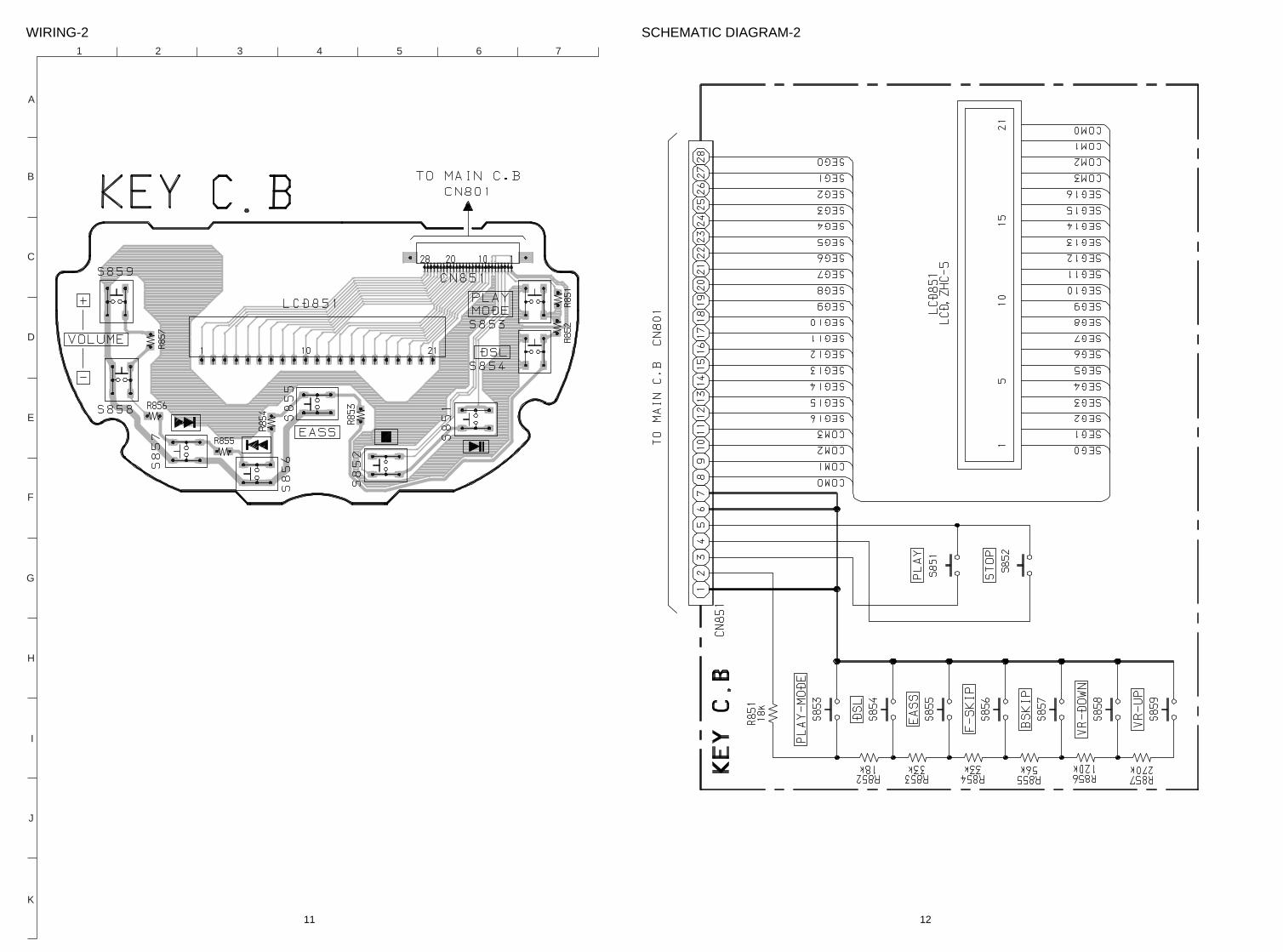
KEY C.B
8Z-HC3-602-010 PWB,KEY(4M) ZHC-3 CN851 87-A60-789-080 C-CONN,28P H 28FLZ-RSM1TB LCD851 8Z-HC3-610-010 LCD,ZHC-3 AIW4186 S851 87-A90-232-080 C-SW,TACT SKQRAA S852 87-A90-232-080 C-SW,TACT SKQRAA
S853 87-A90-232-080 C-SW,TACT SKQRAA S854 87-A90-232-080 C-SW,TACT SKQRAA S855 87-A90-232-080 C-SW,TACT SKQRAA S856 87-A90-232-080 C-SW,TACT SKQRAA S857 87-A90-232-080 C-SW,TACT SKQRAA
S858 87-A90-232-080 C-SW,TACT SKQRAA S859 87-A90-232-080 C-SW,TACT SKQRAA
87
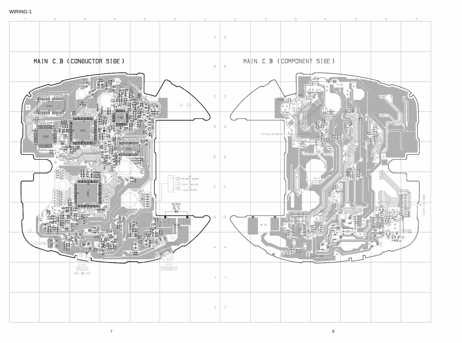
WIRING-17 6 5 4 3 2 1 1 2 3 4 5 6 7
A
B
C
D
E
F
G
H
I
J
A
B
C
D
E
F
G
H
I
J
109
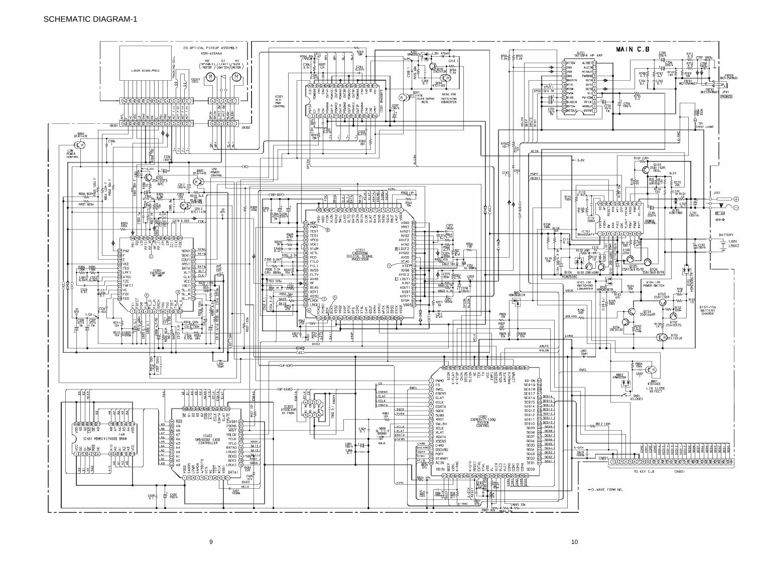
SCHEMATIC DIAGRAM-1
1211
1 2 3 4 5 6 7
A
B
C
D
E
F
G
H
I
J
K
WIRING-2 SCHEMATIC DIAGRAM-2
13
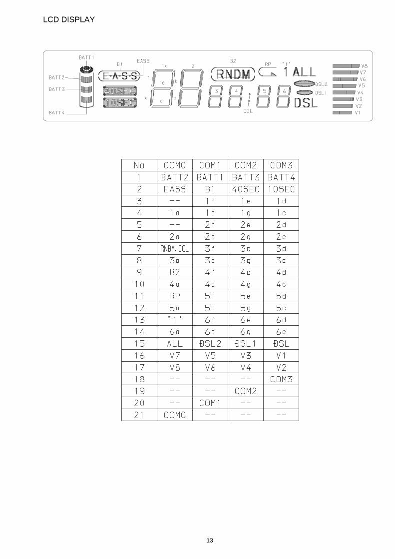
LCD DISPLAY
14
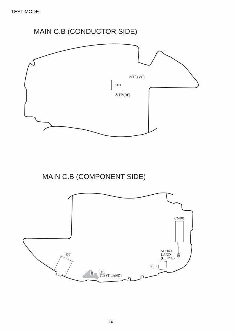
TEST MODE
MAIN C.B (CONDUCTOR SIDE)
IC301
TP (VC)
TP (RF)
TP1(TEST LAND)
J701
S801
SHORTLAND(CLOSE)
CN801
MAIN C.B (COMPONENT SIDE)
15
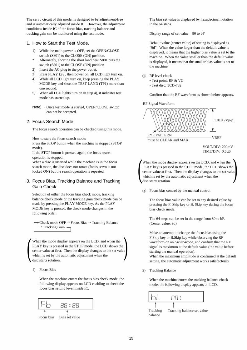
The bias set value is displayed by hexadecimal notationin the 64 steps.
Display range of set value 80 to bF
Default value (center value) of setting is displayed as“9d”. When the value larger than the default value isdisplayed, it means that the higher bias value is set to themachine. When the value smaller than the default valueis displayed, it means that the smaller bias value is set tothe machine.
1 RF level check• Test point: RF & VC• Test disc: TCD-782
Confirm that the RF waveform as shown below appears.
RF Signal Waveform
EYE PATTERNmust be CLEAR and MAX
1.0±0.2Vp-p
VREF
VOLT/DIV: 200mVTIME/DIV: 0.5µS
When the mode display appears on the LCD, and when thePLAY key is pressed in the STOP mode, the LCD shows thecenter value at first. Then the display changes to the set valuewhich is set by the automatic adjustment when thedisc starts rotation.
2 Focus bias control by the manual control
The focus bias value can be set to any desired value bypressing the F. Skip key or B. Skip key during the focusbias check mode.
The 64 steps can be set in the range from 80 to bF.(Center value: 9d)
Make an attempt to change the focus bias using theF.Skip key or B.Skip key while observing the RFwaveform on an oscilloscope, and confirm that the RFsignal is maximum at the default value (the value beforestarting the manual operation).When the maximum amplitude is confirmed at the defaultsetting, the automatic adjustment works satisfactorily
2) Tracking Balance
When the machine enters the tracking balance checkmode, the following display appears on LCD.
Tracking balance set valueTracking balance
The servo circuit of this model is designed to be adjustment-freeand is automatically adjusted inside IC. However, the adjustmentconditions inside IC of the focus bias, tracking balance andtracking gain can be monitored using the test mode.
1. How to Start the Test Mode.
1) While the main power is OFF, set the OPEN/CLOSEswitch (S801) to the CLOSE (ON) position.
* Alternately, shorting the short land near S801 puts theswitch (S801) to the CLOSE (ON) position.
2) Insert the AC plug to the power outlet.3) Press PLAY key , then power on, all LCD light turn on.4) While all LCD light turn on, keep pressing the PLAY
MODE key and short the TEST LAND (TP1) more thanone second.
5) When all LCD lights turn on in step 4), it indicates testmode has started up.
Note) • Once test mode is started, OPEN/CLOSE switchcan not be accepted.
2. Focus Search Mode
The focus search operation can be checked using this mode.
How to start the focus search mode:Press the STOP button when the machine is stopped (STOPmode).If the STOP button is pressed again, the focus searchoperation is stopped.When a disc is inserted while the machine is in the focussearch mode, the disc does not rotate (focus servo is notlocked ON) but the search operation is repeated.
3. Focus Bias, Tracking Balance and TrackingGain Check
Selection of either the focus bias check mode, trackingbalance check mode or the tracking gain check mode can bemade by pressing the PLAY MODE key. As the PLAYMODE key is pressed, the check mode changes in thefollowing order.
Check mode OFF ™ Focus Bias ™ Tracking Balance™ Tracking Gain
When the mode display appears on the LCD, and when thePLAY key is pressed in the STOP mode, the LCD shows thecenter value at first. Then the display changes to the set valuewhich is set by the automatic adjustment when thedisc starts rotation.
1) Focus Bias
When the machine enters the focus bias check mode, thefollowing display appears on LCD enabling to check thefocus bias setting level inside IC.
Focus bias Bias set value
( (
( (
16
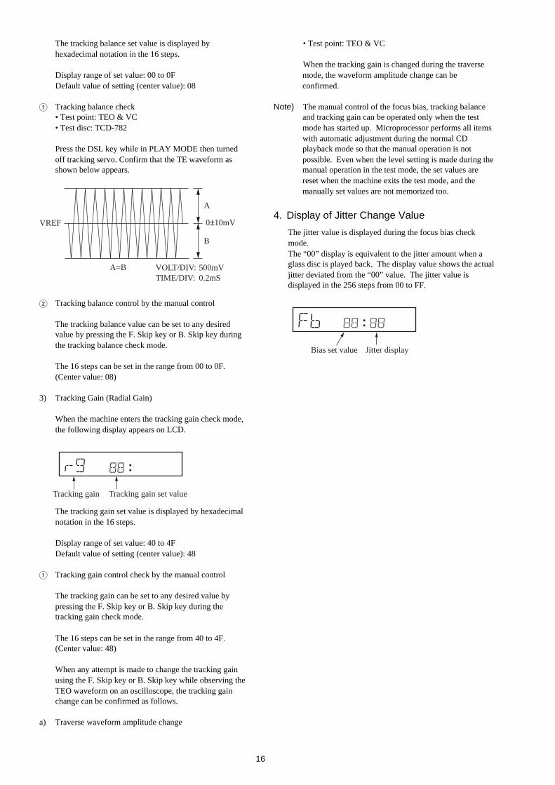
The tracking balance set value is displayed byhexadecimal notation in the 16 steps.
Display range of set value: 00 to 0FDefault value of setting (center value): 08
1 Tracking balance check• Test point: TEO & VC• Test disc: TCD-782
Press the DSL key while in PLAY MODE then turnedoff tracking servo. Confirm that the TE waveform asshown below appears.
0±10mV
A
B
VREF
A=B VOLT/DIV: 500mVTIME/DIV: 0.2mS
2 Tracking balance control by the manual control
The tracking balance value can be set to any desiredvalue by pressing the F. Skip key or B. Skip key duringthe tracking balance check mode.
The 16 steps can be set in the range from 00 to 0F.(Center value: 08)
3) Tracking Gain (Radial Gain)
When the machine enters the tracking gain check mode,the following display appears on LCD.
Tracking gain Tracking gain set value
The tracking gain set value is displayed by hexadecimalnotation in the 16 steps.
Display range of set value: 40 to 4FDefault value of setting (center value): 48
1 Tracking gain control check by the manual control
The tracking gain can be set to any desired value bypressing the F. Skip key or B. Skip key during thetracking gain check mode.
The 16 steps can be set in the range from 40 to 4F.(Center value: 48)
When any attempt is made to change the tracking gainusing the F. Skip key or B. Skip key while observing theTEO waveform on an oscilloscope, the tracking gainchange can be confirmed as follows.
a) Traverse waveform amplitude change
• Test point: TEO & VC
When the tracking gain is changed during the traversemode, the waveform amplitude change can beconfirmed.
Note) The manual control of the focus bias, tracking balanceand tracking gain can be operated only when the testmode has started up. Microprocessor performs all itemswith automatic adjustment during the normal CDplayback mode so that the manual operation is notpossible. Even when the level setting is made during themanual operation in the test mode, the set values arereset when the machine exits the test mode, and themanually set values are not memorized too.
4. Display of Jitter Change Value
The jitter value is displayed during the focus bias checkmode.The “00” display is equivalent to the jitter amount when aglass disc is played back. The display value shows the actualjitter deviated from the “00” value. The jitter value isdisplayed in the 256 steps from 00 to FF.
Bias set value Jitter display

17
IC BLOCK DIAGRAMIC, BA6655AFV
IC, BH6508FS
18
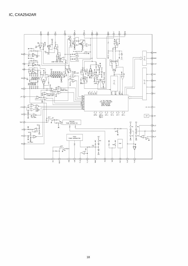
IC, CXA2542AR
19
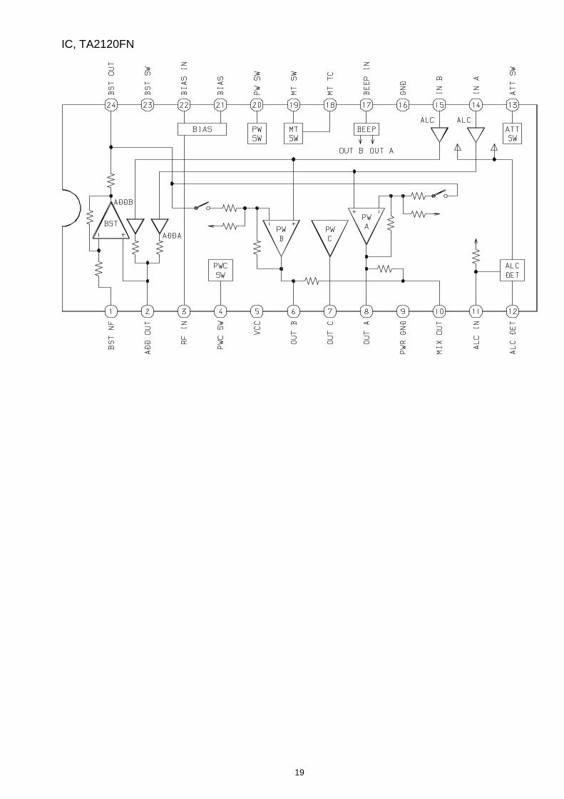
IC, TA2120FN
20
Pin Name
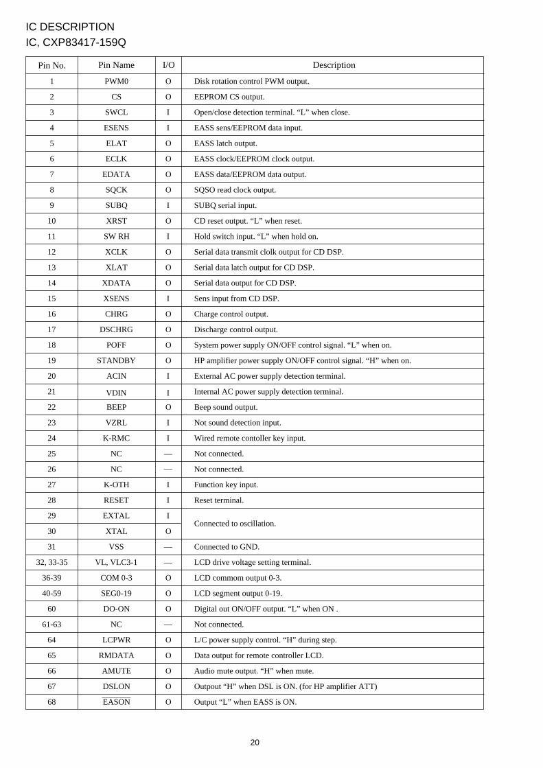
IC DESCRIPTIONIC, CXP83417-159Q
1 PWM0 O Disk rotation control PWM output.
2 CS O EEPROM CS output.
3 SWCL I Open/close detection terminal. “L” when close.
4 ESENS I EASS sens/EEPROM data input.
5 ELAT O EASS latch output.
6 ECLK O EASS clock/EEPROM clock output.
7 EDATA O EASS data/EEPROM data output.
8 SQCK O SQSO read clock output.
9 SUBQ I SUBQ serial input.
10 XRST O CD reset output. “L” when reset.
11 SW RH I Hold switch input. “L” when hold on.
12 XCLK O Serial data transmit clolk output for CD DSP.
13 XLAT O Serial data latch output for CD DSP.
14 XDATA O Serial data output for CD DSP.
15 XSENS I Sens input from CD DSP.
16 CHRG O Charge control output.
17 DSCHRG O Discharge control output.
18 POFF O System power supply ON/OFF control signal. “L” when on.
19 STANDBY O HP amplifier power supply ON/OFF control signal. “H” when on.
20 ACIN I External AC power supply detection terminal.
21 VDIN I Internal AC power supply detection terminal.
22 BEEP O Beep sound output.
23 VZRL I Not sound detection input.
24 K-RMC I Wired remote contoller key input.
25 NC — Not connected.
26 NC — Not connected.
27 K-OTH I Function key input.
28 RESET I Reset terminal.
29 EXTAL IConnected to oscillation.
30 XTAL O
31 VSS — Connected to GND.
32, 33-35 VL, VLC3-1 — LCD drive voltage setting terminal.
36-39 COM 0-3 O LCD commom output 0-3.
40-59 SEG0-19 O LCD segment output 0-19.
60 DO-ON O Digital out ON/OFF output. “L” when ON .
61-63 NC — Not connected.
64 LCPWR O L/C power supply control. “H” during step.
65 RMDATA O Data output for remote controller LCD.
66 AMUTE O Audio mute output. “H” when mute.
67 DSLON O Outpout “H” when DSL is ON. (for HP amplifier ATT)
68______________
EASON O Output “L” when EASS is ON.
DescriptionPin No. I/O

21
69 EMPI O Diemphasis control terminal. “H” when on.
70 VCC — Power supply input.
71 TX O Sub clock oscillation output.
72 TEX I Sub clock oscillation input.
73 NC — Connected to VDD.
74 SLCON O Sled motor control.
75 SPCON O Spindle motor control.
76 CNIN I Track count input.
77 K-STOP I Stop key input. “H” when ON.
78 K-PLAY I Play key input. “H” when ON.
79 SCOR I Sub code SYNC SCOR input.
80 — — Connected to VDD.
I/O DescriptionPin No. Pin Name
22
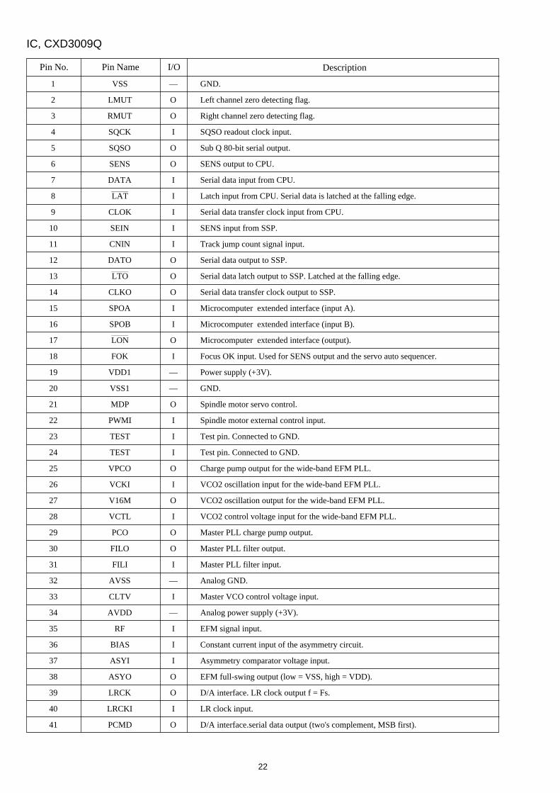
1 VSS — GND.
2 LMUT O Left channel zero detecting flag.
3 RMUT O Right channel zero detecting flag.
4 SQCK I SQSO readout clock input.
5 SQSO O Sub Q 80-bit serial output.
6 SENS O SENS output to CPU.
7 DATA I Serial data input from CPU.
8________
LAT I Latch input from CPU. Serial data is latched at the falling edge.
9 CLOK I Serial data transfer clock input from CPU.
10 SEIN I SENS input from SSP.
11 CNIN I Track jump count signal input.
12 DATO O Serial data output to SSP.
13________
LTO O Serial data latch output to SSP. Latched at the falling edge.
14 CLKO O Serial data transfer clock output to SSP.
15 SPOA I Microcomputer extended interface (input A).
16 SPOB I Microcomputer extended interface (input B).
17________
LON O Microcomputer extended interface (output).
18 FOK I Focus OK input. Used for SENS output and the servo auto sequencer.
19 VDD1 — Power supply (+3V).
20 VSS1 — GND.
21 MDP O Spindle motor servo control.
22 PWMI I Spindle motor external control input.
23 TEST I Test pin. Connected to GND.
24 TEST I Test pin. Connected to GND.
25 VPCO O Charge pump output for the wide-band EFM PLL.
26 VCKI I VCO2 oscillation input for the wide-band EFM PLL.
27 V16M O VCO2 oscillation output for the wide-band EFM PLL.
28 VCTL I VCO2 control voltage input for the wide-band EFM PLL.
29 PCO O Master PLL charge pump output.
30 FILO O Master PLL filter output.
31 FILI I Master PLL filter input.
32 AVSS — Analog GND.
33 CLTV I Master VCO control voltage input.
34 AVDD — Analog power supply (+3V).
35 RF I EFM signal input.
36 BIAS I Constant current input of the asymmetry circuit.
37 ASYI I Asymmetry comparator voltage input.
38 ASYO O EFM full-swing output (low = VSS, high = VDD).
39 LRCK O D/A interface. LR clock output f = Fs.
40 LRCKI I LR clock input.
41 PCMD O D/A interface.serial data output (two's complement, MSB first).
DescriptionPin No. Pin Name I/O
IC, CXD3009Q
23
42 PCMDI I D/A interface.serial data input (two's complement, MSB first).
43 BCK O D/A interface. Bit clock output.
44 BCKI I D/A interface. Bit clock input.
45 VSS2 — GND.
46 VDD2 — Power supply (+3V).
47 XUGF O XUGF output. Switch to MNT1 or RFCK output by a command. (Not connected)
48 XPCK O XPLCK output. Switch to MNT0 output by a command. (Not connected)
49 GFS O GFS output. Switch to MNT3 or XRAOF output by a command.
50 C2PO O C2PO output. Switch to GTOP output by a command. (Not connected)
51 XTSL I Crystal selector input. Low: 16.9344MHz; High: 33.8688MHz.
52 C4M O 4.2336MHz output. (Not connected)
53 DOUT O Digital out output.
54 EMPH OOutput a high signal when the playback disc has emphasis, and a low signal when
there is no emphasis. (Not connected)
55 EMPHI I Input a high signal when de-emphasis is on, and a low signal when de-emphasis is off.
56 WFCK O WFCK output. (Not connected)
57 SCOR O Output a high signal when either subcode sync S0 or S1 is detected.
58 SBSO O Sub P to W serial output.(Not connected)
59 EXCK I SBSO readout clock input.
60 VSS3 — GND.
61 VDD3 — Power supply (+3V).
62 SYSM I Mute input. Active when high.
63 AVSS — Analog GND.
64 AVDD — Analog power supply (+3V).
65 AOUT-L O Left–channel analog output.
66 AIN-L I Left-channel operational amplifier input.
67 LOUT-L O Left-channel line output.
68 AVSS — Analog GND.
69 XVDD — Power supply for master clock.
70 XTAI I Crystal oscillation circuit input. Input the external master clock via the pin.
71 XTAO O Crystal oscillation circuit output.
72 XVSS — GND for master clock.
73 AVSS — Analog GND.
74 LOUT-R O Right-channel line output.
75 AIN-R I Right-channel operational amplifier input.
76 AOUT-R O Right-channel analog output.
77 AVDD — Analog power supply (+3V).
78 AVSS — Analog GND.
79________
RST I System reset. Reset when low.
80 VDD — Power supply (+3V).
I/O DescriptionPin No. Pin Name
24
1 VDD2 — Power supply.
2 EASON — Not connected.
3 COMP — Not connected.
4 EAMOD — Not connected.
5 4/5BITS — Not connected
6 VSS2 — Connected to GND
7 DIT — Not connected.
8___________
TEST — Not connected.
9 MCLK I 16.9344MHz clock input.
10 VSS1 — Connected to GND.
11 DATAI I Audio serial input data.
12 LRCKI I Audio serial input LR clock data.
13 BCKI I Audio serial input bit clock data.
14 BCKO O Audio serial output bit clock data.
15 LRCKO O Audio serial output LR clock data.
16 DATAO O Audio serial output data.
17 YFLG I RAM over-flow flag of signal processing IC.
18 YCLK I Frame clock for crystal oscillator system.
19 YBLCK I Subcode block cloke signal.
20________
RST I System reset terminal.
21 ESENS O Microprocessor interface status output.
22 VDD1 — Power supply.
23 EMUTE I Force mute termial.
24 ELA T I Microprocessor interface latch clock input.
25 EDATA I Microprocessor interface serial data input.
26 ECLK I Microprocessor interface shift clock input.
27 A10 — Not connected.
28________
CAS O________
D-RAM/CAS control output.
29-32 D2, D3, D0, D1 I/O D-RAM data input/output 2, 3, 0, 1.
33______
WE O______
D-RAM WE control.
34________
RAS O________
D-RAM RAS control.
35-40 A9-A4 O D-RAM address 9-4.
41-44 A0-A3 O D-RAM address 0-3.
IC, SM5904AF
DescriptionPin No. Pin Name I/O
2625
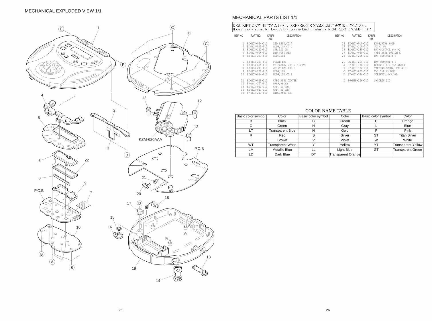
MECHANICAL EXPLODED VIEW 1/1
E
E
C
C
B
D
B
B
A
111
2
1212
12
KZM-620AAA
P.C.B
5
22
P.C.B
6
89
10
7
4
3
21
20
19
16
15
17
18
14
13
REF. NO PART NO. KANRI DESCRIPTIONNO.
REF. NO PART NO. KANRI DESCRIPTIONNO.
MECHANICAL PARTS LIST 1/1
Basic color symbol Color Basic color symbol Color Basic color symbol ColorB Black C Cream D OrangeG Green H Gray L BlueLT Transparent Blue N Gold P PinkR Red S Silver ST Titan SilverT Brown V Violet W White
WT Transparent White Y Yellow YT Transparent YellowLM Metallic Blue LL Light Blue GT Transparent GreenLD Dark Blue DT Transparent Orange
COLOR NAME TABLE
1 8Z-HC3-024-310 LID ASSY,CD A 2 8Z-HC3-015-010 HLDR,LID CD C 3 8Z-HC3-212-010 SPR,LID CD 4 8Z-HC3-006-010 BTN,CONT RBR 5 8Z-HC3-203-010 HLDR,BTN
6 8Z-HC3-201-010 PLATE,LCD 7 8Z-HC3-605-010 FF-CABLE, 28P 0.5 53MM 8 8Z-HC3-211-010 JOINT,LCD ZHC-3 9 8Z-HC3-202-010 HLDR,LCD 10 8Z-HC3-014-010 HLDR,LID CD B
11 8Z-HC3-018-110 CABI ASSY,CENTER 12 88-HV1-207-010 DMPR,MECHA 13 8Z-HC3-012-110 CAP, DC RBR 14 8Z-HC3-011-110 CAP, HP RBR 15 87-HC3-211-010 RING,KNOB RBR
16 8Z-HC3-010-010 KNOB,RTRY HOLD 17 87-HC3-210-010 JOINT,SW 18 8Z-HC3-230-010 BAT-CONTACT,(+)(-) 19 8Z-HC3-025-010 CABI ASSY,BOTTOM A 20 8Z-HC3-215-010 BAT-CONTACT,(-)
21 8Z-HC3-214-010 BAT-CONTACT,(+) A 87-067-736-010 SCREW,1.4-2 BLK NLOCK B 87-067-732-010 TAPPING SCREW, VT1.4-3 C 87-067-869-010 V+1.7-8 HL BLK D 87-067-384-010 SCREWVT1.4-3.5HL
E 86-HSB-226-010 S-SCREW,LID
27
REF. NO PART NO. KANRI DESCRIPTIONNO.
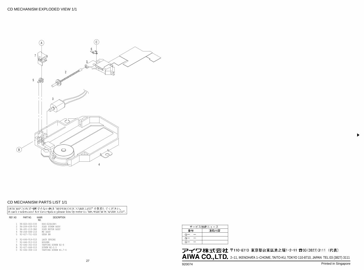
1 98-820-063-030 KSS-620A(RP) 2 9X-264-638-910 SLED SCREW ASSY 3 9A-491-219-9A0 SLED MOTOR ASSY 4 9X-264-648-210 MD ASSY 5 92-627-751-020 GEAR BN
6 92-646-914-010 LACK SPRING 7 92-646-913-010 HOLDER A 92-646-352-010 TAPPING SCREW B2-8 B 92-627-668-010 SCREW M2-2.5 C 92-646-358-110 TAPPING SCREW B1.7-4
CD MECHANISM EXPLODED VIEW 1/1
CD MECHANISM PARTS LIST 1/1
1
2
3
4
5
6
7
B
A C
920074 Printed in Singapore
2–11, IKENOHATA 1–CHOME, TAITO-KU, TOKYO 110-8710, JAPAN TEL:03 (3827) 3111