Embed Size (px)
Citation preview

DIGITAL DELAY
SDD-2000
SERVICE MANUAL
CONTENTS
1. SPECIFICATIONS 2
2. STRUCTURAL DIAGRAM 3
3. BLOCK DIAGRAM 7
4. CIRCUIT DIAGRAM 8
5. PC BOARD 15
6. CIRCUIT DESCRIPTION 19
7. TROUBLE SHOOTING CHART 21
8. CHECK AND ADJUSTMENT PROCEDURE 23
9. REFERENCE DATA 25
10. PARTS LIST 27
KEIO ELECTRONIC LABORATORY CORPORATION
TOKYO/JAPAN

1. SPECIFICATIONS
Input Input level:
Impedance:
Max clip level:
Output (Unity) Output level:
Impedance:
Max clip level:
Frequency 20Hz ~ 20KHz,
response 30Hz ~ 18KHz,
(X1 mode)
30Hz~4.5KHz,
(X4 mode)
-35dBm
-10dBm
47kft
500kft
+6dBm
+19dBm
-35dBm
-10dBm
600ft
600ft
600ft
600ft
-20dBm (Direct)
-20dBm (Effect)
+6dBm (Direct)
+3dBm (Effect)
±1dB (Direct)
+1dB,-3dB (Effect)
+1dB, -3dB (Effect)
• Dynamic range
• S/N ratio
• Distortion
• Delay time
Feedback
• Modulation
• Dimensions
• Weight
• Power supply
voltage
90dB (IHF) (Effect) or more
95dB (IHF) (Direct) or more
80dB(IHF) (Effect)
0.05% (Direct)
0.1% (Effect)
0 ~ 4368msec (1msec step)
0~ 1092msec (1 ~ 10msec- 1msec
step) (X1 mode)
0 ~ 4368msec (X4 mode)
63 steps
0 ~ 31 (Positive phase) 0: 0%,
33: 110%
0^-31 (Opposite phase) 0: 0%,
-31:110%
Waveform: Triangle wave (A)
Modulation frequency: 0.1 Hz ~ 10Hz
(Frequency 0:0.1Hz, 31: 10Hz)
Delay time modulation range: 2:1
(Intensity 31)
482 (W) X44(H)X344(D) mm
4.5kg
AC100V#50/60Hz
• Power
consumption
• Accessories
Options
17W
Rack mounting kit (4 screws,
4 washers)
Signal cord, MIDI cable, FootSW
(PS-1, S-2), IU rack case
-2-

2. STRUCTURAL DIAGRAM
PART No.
A
B
C
0
E
F
G
H
PART NAME
FEB3x6ZMC
FE B 3»10 BZMC
FE B 4«8 BZMC
TP2GB 3»6 BZMC
FHN 3 ZMC
FHN 4 ZMC
VN7ZMC
VN9ZMC
QTY
26
5
1
13
5
1
3
1
PART No.
1
2
3
4
5
6
7
8
9
10
11
12
13
14
IS
16
17
18
19
20
21
22
23
24
25
26
27
PART NAME
CHASSIS
FRONT CHASSIS
METAL FITTING OF FRONT PANEL L
METAL FITTING OF FRONT PANEL R
METAL FITTING OF PHONE JACK
HEAT SINK
METAL FITTING OF BUSHING
VR HOLDER
SHIELDING PLATE
RUBBER FEET
KLM-825
KLM-829
KLM-831
KLM-832
KLM-833
TACT SW KNOB
TACT SW KNOB
TACT SW KNOB
POWER TRANSFORMER TA-802
TB-802
VR
ROTARY ENCOOER
POWER SW
BUSHING
WIRE BAND
WIRE BAND
PLASTIC RIVET
SNAP PLATE
PART CODE
64069300
64069400
64063600
64063601
64069600
64063800
64064000
79022102
63000300
50007800
34082610
34082910
34083100
34083200
34083300
62011001
62011202
62011000
40008900
40009000
36019100
37003100
37506100
54005300
54007100
54011000
45402400
-3- -4-

PART No.
A
B
C
0
PART NAME
TP2G B 3x6 BZMC
TP2G F 3*8 BZMC
FEHS 4x8 BZMC
WK4 BZMC
OTY
11
4
4
4
PART No.
2
3
5
6
7
8
9
10
PART NAME
CHASSIS
FRONT PANEL
COVER
FRONT PANEL BOARO
NAME PLATE
RADIATION MASK
LEO FILTER
VR KNOB
POWER SW KNOB
ROTARY VR (SW) KNOB SMALL
PART COOE
64069300
64069200
64069500
64063700
68600700
55005100
63001000
62013200
62011100
62007400
-5--6-

CO■
00
5o
g
*
HEAD
ROOM
/ ._ DELAY OFF EMPHASIS FEEDBACK LEVEL
PROGRAMMABLE
PROG.NO DATA/TIM£(n>5) QlSPLAY
o o o o o o

00
[k"lM-833~~]CN9! |CN9
T10I TA802orlB802.1 1
o
O
H
a
I
SKI :PME265MC533 100V
1 17V
220V
24UV
Fl. F2
250V 1A
250V.T500mA
F3
125v 2A
250V. T1A
F4
250V 0.5A
250V.T315mA
T101
TA-802
TB-8C2

KLM-831
DATA/TlME(mS)
KLM-831
-9-

o
00
(a)

6. CIRCUIT DESCRIPTION
1. KLM-833 Analog Circuit
Audio signal route
Level of Audio signal input from Connector CN-11 pin 2
is decided by Relay RY1 which is controlled by Attenuator
SW. Level of Audio signal amplified by 1/2 IC31 is change
able by Input Level VR (VR101). Audio signal re-amplified
by 1/2 IC31 (4558) is sent to each of (1) 2 kinds of Low-
pass filter LPF-1, LPF-2 (2) Direct Out VR 102, 1/2 IC36
and (3) Q24.
Q24 is amplifier for trigger controlled by Audio signal
sending trigger signal to CPU port PA7 (IC23, pin 8)
while sampling and start sampling according to Audio
signal level.
IC35 is an Analog Switch selecting which Audio signal
will be output, one from LPF-1, one from LPF-2 or no
signal (OFF). This IC is controlled by Gate Array. In
this case, OFF is selected to off Audio signal and make
Audio signal not to be sent to A/D while REC CANCEL.
This IC35 is controlled by Gate Array IC22 pin 29 (SOFF
terminal). (SOFF terminal is "L" while REC CANCEL)
Selecting of LPF-1, LPF-2 is made by CPU IC23. This is,
CPU address is decoded by decoder IC56 and let IC47
latch data. Filter selecting signal is controlled by IC47
latch output pin 15. When delay time mode is x 4, this
terminal comes to be "H" and LPF-1 (4.5KHz) is selected.
1/2 IC33 (Pin 1,2,3) works as Pre-emphasis, and Mix Amp
of FEED BACK and 1/2 IC33 (Pin 5,6,7), IC32, IC37
work as Analog Compander (Compressor+Expander)
and Audio signal.
1/2 IC13 is an Analog Switch and works as a Bypass Switch
of Analog Compander Circuit. This IC is controlled by
pin 27 :COMP Terminal of Gate Array IC22. ("L" at Delay,
"H" at Sampling, Sequencer)
While sampling, it lets compressed Audio signal bypass
Analog Compander Part not to have compressing error.
Output signal (LCOM terminal) of IC13 is output as A/D
signal to Digital Circuit.
D/A signal once digitalized in Digital Circuit changes to
Analog signal after through D/A and is input to IC29, IC32.
IC32 constructs Expander with 1/2 IC34, and IC37.
IC29 constructs Audio Muting Circuit with IC30. 1/2
IC13 is an Analog Switch and works with Compander to
make Audio signal bypass Expander while Sampling.
IC 29: Signal Muting Circuit is VCA which has time
Constance in order not to generate Noise at signal sudden
ON/OFF and smoothen Audio signal while sampling.
This IC works with control signal from CPU PA6 terminal
letting IC30 drive VCA.
IC39 is an Analog Switch selecting which Audio signal
will be output, one from LPF-3, one from LPF-4 or no
signal (=OFF). OFF is selected in order to off delay sound
while REC SYNC SW is ON (Sampling, Sequencer, Trigger
Overdub are ON). When those Switches are ON, Gate Array
IC22 pin 28 (DOFF terminal) becomes "H" and off output
from IC39.
The signal which passes IC39 is de-emphasized at 1/2
IC40 (pin 5,6,7) and go into EFFECT Volume Control
Circuit and FEED BACK Volume Control Circuit.
A) EFFECT Volume Control Circuit
EFFECT Level data from CPU DATA BUS DO - D7
is latched by IC44 and IC44 lets Analog switches IC45,
IC46 control Block R. RM8 to decide EFFECT level.
B) FEED BACK Volume Control
FEED BACK Level Data of CPU DATA BUS is latched
by IC41 and IC41 lets Analog Switches IC42, IC43
control Block R. RM7 to decide FEED BACK level.
Phase of FEED BACK signal output from Block R. RM7
is inverted at 1/2 IC40 (pin 1,2,3).
Analog SW. IC42 selects if normal or inverted and the
feedbacked signal is returned to IC35 output.
(Note: Analog Switch is controlled by CPU DATA
latched by IC41.)
MODULATION PART
FREQ.
At 2/4 IC54 (pin 5,6,7 pin 8,9,10), Triangle Wave Oscillator
Circuit is constructed. Data from CPU DATA BUS is
latched by IC47 and IC47 Analog SW. IC49, IC48 control
RM9 to decide oscillation frequency.
INTENSITY
Data from CPU DATA BUS DATA is latched by IC50
and lets Analog Switch IC51, 52 control Block R. RM10
to be working as attenuator in order to decide MG INT.
IC53 latches Scale Data which is from CPU DATA BUS
By the latched data, IC55 works as D/A and input latched
data to pin 2 of IC54 and mix with basic voltage to control
VCO: IC21 which changes system clock.
2. KLM-833 Digital Circuit
1) Audio Signal Path
A/D signal is made to be S/H by IC15 and 1/2 IC14.
The signal made to be S/H is at IC17 and to be Digital
signal after linearization (12bit) by D/A IC18 and
Succesive Approximation Registers. And memorized
into IC11 — IC14 accordingly.
IC3, IC2 (74HC138) are decoders.
Gate Array reads Delay value from DATA BUS of CPU
and outputs address which accesses D-RAM. And output
data from D-RAM returns to Gate Array and Gate
Array controls IC18 to output D/A signal. Output
data from D/A is made to be S/H at IC16, 1/2 IC14
and output to Analog Circuit as analog signal.
2) System Clock Path
VCO control D/C voltage is sent from Analog Circuit
to IC21 pin 13. With the voltage, IC21 generates and
supplies System Clock to IC22 pin 31. Gate Array IC22
produces Timing which controls each part of SDD-2000.
-19-

KLM-833(1)
I 04 SLt26v«y
j KLM-825A
D.ONO
| KLM-829C
UNLESS OTHERWISE NOTICED
POWER SUPPLY VOLTAGE OF OP AMP +15V AND -15V
ALL DIODES 1SS133 OR 1SS176
CERAMIC CAPACITORS RANK J (5%)
MYLAR CAPACITORS RANK J (57c)
ARE CONNECTED TO KLM-833A (2)
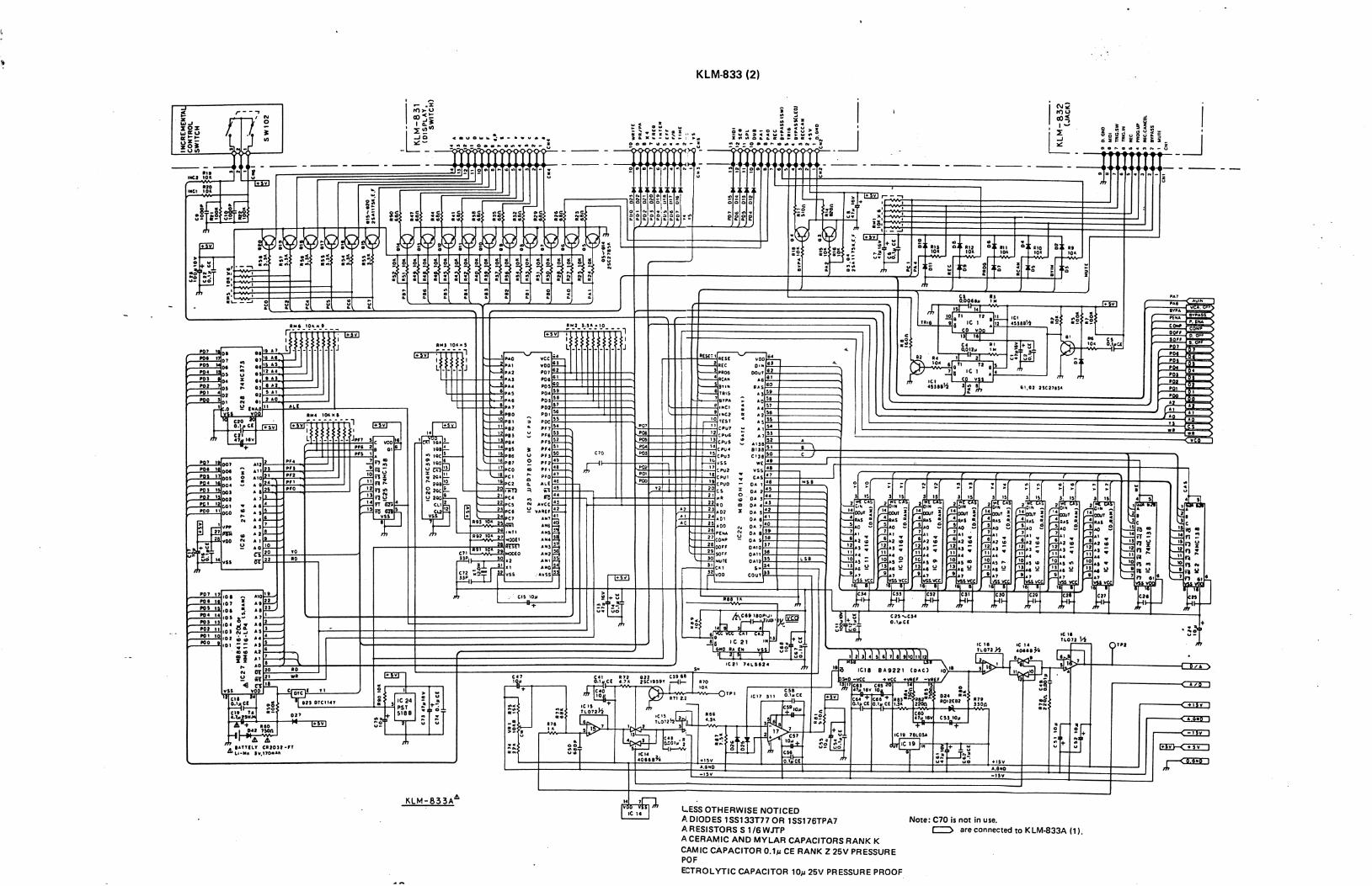
KLM-833 (2)
KLM-833A*
JT<ES3E=]
1 >c" ILESS OTHERWISE NOTICED
ADIODES 1SS133T77OR 1SS176TPA7
A RESISTORS S1/6WJTP
A CERAMIC AND MYLAR CAPACITORS RANK K
CAMIC CAPACITOR 0.1** CE RANK Z 25V PRESSUREPOF
ECTROLYTIC CAPACITOR 10m 25V PRESSURE PROOF
Note:C70 is not in use.
are connected to KLM-833A (1).

5. PC BOARD
KLM-833
- . , Tc V I C90» / C91 \ «24 'te)\\ n,; , ^yi®;® o)>% ©) ©z±^i ©s.. . -8 ©-© ©-©v*©-© f^^^ v
-15- -16-

00
©*
®
r>~i
£ ?-g^
r>~i
lr®i
sL«ll
^
ftOo
-o L
I'
-■»/
1
00ro
CJl
iLoJ
©©
•Loll
yO
-I
©OO
r"®ns
*
o-
aoo
oo©
o
®
^;\
oo©»
*©©,
oo
©o
*o
&_
"oo
o©
©
@
JAGAINST
THE
RISK
OFFI
REI2SOV
T3i5mA|
REPUCE
ONLY
WITH
SAME
TYPE
FUSE.
LL
JJ
00
CO
00ro
CO
O
I
ri
SWI
R2
R5
R6
u do;
RI2
WV*-
••
o
CO
00
CO
ro
O
J2
RI4VNV-
Q3
r.ou
N■ y o
lod= O
<D
u
—-r-«-«r>o—=:—~
a.o
>r*
O>

3) Switch, Control Part
Pulse signal sent from Incremental Controller controls
Internal Counter of Gate Array and it sends Count
value to CPU DATA BUS.
Waveform of the signal sent from Trigger Jack is shapen-
ed at Q1 and at One shot-MuIti of IC1 reformed to pulse
wave. LED displaying of Trigger signal ON/OFF is done
by IC1 and Q2.
Input signals of MUTE, BYPASS, REC CANCEL,
PROG. UP, REC TRIG SW. are input to Gate Array and
sent to CPU as readable data. *
MIDI signal is sent to and controlled by CPU.
Tact Switch on Front Panel is controlled by CPU.
4) CPU
CPU connects IC28 (Latch), IC26 (ROM), IC27 (RAM)
and IC22 (Gate Array) through decoder and controls
each with DATA BUS.
IC20 Counter HC393 devides the signal (S/H) syncro-
nizing with System Clock of Gate Array and sends it to
CPU in order that CPU can read system clock.
i
-20-

7. TROUBLESHOOTING CHART
Note:
Before servicing, make sure that all harnesses are plugged into their connectors.
Problem:Bad LED
indication
Bad MIDI scale.
FREQ, INT
doesn't work.
Check KLM-829
power supply and
confirm proper
± 15V and +5V
voltages.
Trouble is in IC1,
IC2 (±15V), IC3
(+5V), fuse, diodes,
transformer, AC
cord, power switch,
or KLM-833 power
supply line.
Refer to KLM-833
clock adjustment
procedure and
check if clock is
normal.
NO
Check reset circuit.
When power is
turned on: low
to high level;
low is active.
Check IC24,
Q23, IC22, IC23.
Check IC23
x1,x2
terminals.
Check x1, IC23
C71,C72.
YES
Follow
adjustment
procedure.
Check IC53,
IC55, IC21,
IC22.
Does oscilloscope
show normal
waveform at IC23
INT1, INT2
terminals?
(NOTE) WAVEFORM AT DELAY SETTING.
Check IC20
1-pin (S/H)for
ormal input.
Trouble is in IC26
IC27, IC28, IC23
IC22, etc. Check
each chip and bus,
in turn.
Trouble in
IC23 or IC20
Check
IC22, IC20
INT1
INT2
SH
n_TLTL5V
OV
L5V
OV
6.4ms
U LI5V
-21-

No deiay out put,
Check IC13
1 hpm (A/DI on
oscilloscope.
YES
Chr kck (CIS
IS/H output}
1 -p
osc
n on
Hoscope.
Check Q2.,
IC14, 1C15,
IC22 (S/H
OU! put)..
Check 1C22 33-pin
fCOUT input lerfTiitnal}.,
* Th e w«■jve f n r rn qoe s
i h r -o u g h a c o ft's pa ra i ot
so it can be loaded
into IC22asOV-5V
digital data.
Check IC1 /
and IC22.
YES
Check SC22
63-pin {data
output terminal
for DRAM).
Check TP2
<0/A>on
oscilloscope..
NO Check IC18
(DAC)(
and Id6.
YES
Check and
replace IC1 3.
NO
Oh*
! 1 !>■
a $c
;ck IC35
p i n o n
ilsoicope.
YES Check JC33,
1C37, and
IC32.
Check and
replace IC35.
Can you
a waveform for
IC40 7-pin on
I he o
Can you observe
IC38 1-pin on
the osciHoscope?
Check 1C44,
5P IC46,
RM8,
Trouble in 1/2 IC38,
,1C38,, jacks,, or circuit
board pattern.
-22-

8. CHECK AND ADJUSTMENT PROCEDURE
Caution:
a. This product has been adjusted completely at the
f ac i: o f y be for e s h i pme n t.
Therefore, do not adjust any points other than those
seemed necessary,
b, Wait at feast 10 minutes after turning on the power
before rnaking any adjustments,.
1) Clock check and adjustment — 1
,H Setting: (any program number OK) Set TUNE VR on
rear panel to center.
ai r sw :
t o ;
D. TIM £
0
LEVEL VR !
0
INTENSITY
0
DIRECT VR
0
FRECX.
: 0
EFFECT 1
0
TIME k. 4
0 F F
F.BACK
0
MODE
DELAY
n) Connect frequency counter to TP1 test point of KLM-
833 and observe frequency.
c) Check if value of the counter is 4 Oik Hz ! lOOHz.
cl'i Adjust VR8 to obtain above value if the observed value
iS out of above range.
2) Clock check and adjustment — 2
a? Setting: (any program number OK) Set TUNE VR on
rear panel to center,
<TT S'/y
1 0
J.TIME
o ""
LEVEL VR
7
INTENSITY
: o
DIRECT VR
'"" o
FREO.
o " '
EFFECT
o
TIME :k 4
OF?
F.BACK
~ o " "
MODE
* Off the MIDI SW. and record any sound with SEQ
MODE.
b) Connect frequency counter to TP1 and observe fre
quency.
el ON the MIDI SW., and play MIDI Keyboard such as
POLY-800,
Cl Key
C2 Key
C3 Key
B3 Key
value on counter
10rOO0Hz
20,,OOOHz
40,OO0Hz
7 5,644 Hz
Bend Up (Bend Range Max) BO/QQOHz
Note:.
MIDI: Receive CH must be ICiH.,
MIDI ed i t i n f orm a t io n mu s t be X 4 m od e.,
Support note range must be Cl,
31 LFO check and adjustment
a) Sa t1 \ n cj: i a n y P rog r am n umbe r O K)
Al f SW
10
D.TIME
0
t EVEL VR
0
i IN TENS 11 V
1 " ' o
DIRECT VR
0
FREQ.
0
EFFECT
0
\ TIME x 4
OFF
F BACK
0
MODE
DELAY
b) Connect oscilloscope (0.5V/div, 0.5V/div, DC) to TP3
on Kt IV!-833 and observe waveform described below,
GNDA "
/ \ ./\
,/\/
\
A
/ \■ /
Fig, 1
c} C o fi f s rm s f t o p of t h e w ave f o r rn i s 0 V.
cl) Adjust VR6 to obtain above waveform if observed
wav e f o rm i s d i f f e r e n t from t h e a bove d e sc r i p t i o n,
4) Maximum output level cheek and adjustment
a) Set11 n g: (a n y p r ogram n u rn be r O K 31
ai rsw
10
D.TiME
0
1 EVEL VR
'?
INTENSITY
0
DIRECT VR
«
FREO.
0
EFFECT
TIME x 4
OFF
F.BACK 10 i
MODE ;
DEI AY
any value OK
b( Connect standard signal generator (1KHz sine wave) to
this unit's Input Jack,,
c} Co n n ec t osc i 11 ©scope (2V /'cl j v, 50/usec/di v, A C} to T P 2
on KLlvi-833 and observe waveform described as below.
To get the click waveform as below, adjust output
v o 1 u me o f sta nd a rd s i cj n a I g e n e r a to r.
i'S !\ I s x"\ I \ r \
\f "•,.
fi -\ / - \J U I / l
GOOD
Fig, 2
d) Check if the observed waveform is GOOD, If not,, adjust
VR1 on KLM-833.
BAD BAD
clj Confirm if the value on the counter is within 80KHz
e) Adjust VR7 to obtain above value if the observed value
ts out of above range.
■•- 23 •

5) Analog Converter check and adjustment
a) Setting: (any program number OK)
ATTSW
-10
D.TIME
0
LEVEL VR
7
INTENSITY
0
DIRECT VR
0
FREQ.
0
EFFECT
22
TIME x 4
OFF
F.BACK
0
MODE
DELAY
b) Input sine toneburst wave (=Sine Pulse Wave) (level:
10dBm, Freq.: 400Hz, width: 100msec) to Input Jack
and observe EFFECT OUT with oscilloscope.
*l*2
100 msec
*3
Fig. 3
c) When you cannot get correct waveform as above;
Adjust linearity at *3 with VR3, or adjust VR4 on
KLM-833 to minimize DC drift in part *3 of the wave
form. ("Description of the above figure is almost same
as Service Manual for SDD-1000. Please refer to it.)
(Page 16)
7) VCA check and adjustment
a) Setting: (any program number OK)
ATT SW.
-10
TIME
0
LEVELVR
7
INTENSITY
0
DIRECT VR
0
FREQ.
0
EFFECT
31
TIME x 4
OFF
F.BACK
0
MODE
SAMPLING
b) Input SG (sine wave of 1KHz, 2.5V P-P) to Input
Jack and play sampling.
c) Connect MIDI Keyboard and playback sampling note,
(play any key continuously)
d) Connect oscilloscope (DC 0.2V/div, 20msec/div) to
EFFECT OUT and observe waveform as below.
Key on
NG
Key on Key on
GOOD NG
Fig. 4
e) Confirm if the observed waveform is GOOD. If not,
adjust VR2 on KLM-833.
6) Feed back check and adjustment
a) Setting: (any program number OK)
ATTSW
-10
D.TIME
120msec
LEVEL VR
7
INTENSITY
0
DIRECT VR
0
FREQ.
0
EFFECT
22
TIME x4
OFF
F.BACK
30
MODE
DELAY
b) Connect oscilloscope (AC 0.5V/div, 0.5msec/div)
to EFFECT OUT and confirm ringing when input
sineburst wave (Freq.: 400Hz, width: 100msec) to
Input Jack.
c) Set parameter value of FEED BACK to 28 and confirm
no ringing when input the same sineburst wave as b).
d) Adjust VR5 not to generate ringing in case ringing
occurs in above c).
e) Confirm if ....
no ringing occurs without any input.
ringing occurs with parameter value of FEED BACK
is even -30±1 and phase changes.
-24-

9. REFERENCE DATA
8 BIT D/A CONVERTER HA17408
BLOCK DIAGRAM
MSB
Ai A2 A3 A4 A5
LSB
LOGIC INPUT SWITCH
1 1 1 I I
VREF H (15
2) GND
16J Compensation
PIN CONFIGURATION
nc|T
gnd[T
vee[T
(MSB) Ai |T
A2[6
A3Q
A4[T
Compensation
15] vref h
2f]vREF (+)
H)vcc
T5J A8 (LSB)
n]A7
To] A6
T| A5
12 BIT D/A CONVERTER BA9221
BLOCK DIAGRAM PIN CONFIGURATION
MSB LSB
VccGND/VlcB0 B, B2 B, B, B, 8, B, B8 B, 8l0 B, ,
920 Jli3 ?1 <f2 <f3 <j>4 <?5 <f6 <?7 <? 8 ?9 ?10 ?11 <? 12
LOGIC INPUT SWITCH DRIVERS
.16 617
COMP VEE
CMOS ANALOG SWITCH mPD6360C VCA BA6110
BLOCK DIAGRAM, PIN CONFIGURATION BLOCK DIAGRAM
I I i
I I I1 I " > CD
-25-

CPU juPD7810
BLOCK DIAGRAM PIN CONFIGURATION
1 •I ILATCH
INC/OEC
SP
EA
V
B
D
E
V
B'
H1
A
c
BUFFER
I
G,R
G,R
PROGRAM
MEMORY
(MPO7811
only)
a
MEMORY
(256-BYTEI
ITINTERNAL DATA BUS ICO
[PSW
SiXALU
8/16)
-
0INST. REG
INST.
OECODER
Note: >jPD7810 doesn't contain program memory
(4 Kbyte). CONTROL CONTROL CONTROL
I!is li
PAO C
PA1 C
'A2 C
PB2 C
PB3C
PB4C
PB5C
PB6C
PB7 C
PCO/TxO C
PCI/RxD C
PC2/SCK C
PC3/INT2 C
PC4/TO C
PC5/CI C
PC6/CO0 C
PC7/COJ C
MA\ C
INT1 C
MODE1 C
RESET C
MODEO C
X2 C
X1 C
2
3
4
5
6
7
8
9
0
1
2
3
4
S
7
8
9
20
21
22
23
24
25
26
27
28
29
30
31
32
^ 6463
62
61
60
59
58
57
56
55
54
53
52
51
50
48
47
46
45
44
43
42
41
40
39
38
37
36
35
34
33
3VQ0
3 PD7
3 PD6
3 PD5
3 PD4
3 PD3
3 PD2
3PD1
3PD0
3 PF7
3PF6
0 PF5
3 PF4
3 PF3
0 PF2
0 PF1
0 PFO
0 ALE
0 VTE
0 R"D"
0 AVcc
0 VAREF0 AN7
0 AN6
O AN5
O AN4
0 AN3
0 AN2
0 AN1
13 AN0
0 AVSS
GATE ARRAY MB60H144
PA7-0
PB7-0
PC7-0
PD7-0
PF7-0
NMI
MODE 0.1
PIN
: Port A
: Port B
: Port C
: Port D
: Port F
NAMES
X1, X2
AN7-0
RD
WR
ALE
: Non Maskable Interrupt RESET
: Mode 0, 1
: Crystal
: Analog Input
, : Read Strobe
: Write Strobe
: Address Latch Enabl
: Reset
PIN CONFIGURATION PIN DEFINITIONS
64 63 62 61 60 S9 58 57 66 65 54 S3 52 51 50 49 48 47 46 45 44 43 42 41 40 39 38 37 36 35 34 33
nnnnnnnnnnnnnnnnnnnflnnnrnnnnnnnn
EJECTOR WARK
o
UUUUUUUUUJJUU9 20 21 22 23 24 25 26 27 28 29 30 31 32
Pin
no.
1
2
3
4
5
6
7
8
9
10
11
12
13
14
15
16
I/O
I
I
I
I
I
I
0
I
I
I
I/O
I/O
I/O
I/O
I/O
-
Pin
name
RESE
REC
PROG
RCAN
BYIN
TRIG
BYPA
INC1
INC2
TEST
CPU 7
CPU6
CPU 5
CPU4
CPU3
VSS
Pin
no.
17
18
19
20
21
22
23
24
25
26
27
28
29
30
31
32
I/O
I/O
I/O
I/O
I
I
I
I
I
I
0
0
0
0
0
I
-
Pin
name
CPU2
CPU1
CPUO
CS
WR
RD
AD2
AD1
ADO
PENA
CONP
DOFF
SOFF
MUTE
CK1
VDD
Pin
no.
33
34
35
36
37
38
39
40
41
42
43
44
45
46
47
48
I/O
•
0
0
0
0
0
0
0
0
0
0
0
0
0
0
-
Pin
name
COUT
SH
DA12
DA11
DA10
DA9
DA8
DA7
DA6
DA 5
DA4
DA3
DA2
DA1
CAS
VSS
Pin
no.
49
50
51
52
53
54
55
56
57
58
59
60
61
62
63
64
I/O
0
0
0
0
0
0
0
0
0
0
0
0
0
I
0
-
Pin
name
WE
C138
B138
A138
A7
A1
A5
A2
A4
AO
A3
RAS
A6
DOUT
DIN
VDD
Fujitsu CMOS Gate Array "H" Version Pin Assign
-26-

10. PARTS LIST
PARTS
CODE
PARTS NAME
SPECIFICATIONS
P.C.
BOARD
IDENTIFICATION NO.
FUNCTIONQ'TY
CARBON RESISTORS
10113747
10416268
10416310
10416316
10416322
10416322
10416327
10416333
10416351
10416375
10416382
10416410
10416410
10416411
10416412
10416413
10416422
10416424
10416427
10416430
10416433
10416443
10416447
10416447
10416451
10416456
10416462
10416475
10416482
10416510
10416510
10416512
10416515
10416518
10416520
10416522
10416522
10416527
10416530
10416533
10416536
10416539
10416547
10416551
10416556
S1/4JT4.7M
1 /6JTP 68ft
1/6JTP 100ft
1/6JTP 160ft
1/6JTP 220ft
1 /6JTP 220ft
1/6JTP 270ft
1/6JTP 330ft
1/6JTP 510ft
1/6JTP 750ft
1 /6JTP 820ft
1/6JTP 1.0K
1/6JTP1.0K
1/6JTP 1.1K
1/6JTP 1.2K
1/6JTP1.3K
1/6JTP2.2K
1/6JTP2.4K
1/6JTP2.7K
1/6JTP3.0K
1/6JTP3.3K
1/6JTP4.3K
1/6JTP4.7K
1/6JTP4.7K
1/6JTP5.1K
1/6JTP5.6K
1/6JTP6.2K
1/6JTP7.5K
1/6JTP8.2K
1/6JTP 10K
1/6JTP 10K
1/6JTP 12K
1 /6JTP 15K
1/6JTP 18K
1 /6JTP 20K
1 /6JTP 22K
1/6JTP22K
1/6JTP27K
1/6JTP30K
1/6JTP33K
1/6JTP36K
1/6JTP39K
1/6JTP47K
1/6JTP51K
1/6JTP56K
K LM-833
KLM-832
K LM-833
KLM-832
K LM-833
KLM-832
K LM-833
K LM-832
K LM-833
KLM-832-
K LM-833
K LM-832
K LM-833
2
10
1
1
3
3
1
1
3
3
3
4
10
1
1
1
2
4
1
2
8
1
3
7
1
1
1
1
3
2
52
6
1
2
1
2
10
3
3
4
1
4
2
2
1
PARTS
CODE
10416562
10416568
10416582
10416591
10416591
10416610
10416611
10416615
10416616
10416618
10416620
10416622
10416627
10416633
10416647
10416656
10416662
10416710
10509000
PARTS NAME
SPECIFICATIONS
1 /6JTP 62K
1 /6JTP 68K
1 /6JTP 82K
1/6JTP91K
1/6JTP91K
1/6JTP 100K
1/6JTP 11 OK
1/6JTP 150K
1/6JTP 160K
1/6JTP 180K
1/6JTP200K
1 /6JTP 220K
1 /6JTP 270K
1 /6JTP 330K
1/6JTP470K
1/6JTP560K
1/6JTP620K
1 /6JTP 1.0M
YLCOft
P.C.
BOARD
K LM-833
KLM-832
K LM-833
KLM-832
K LM-833
KLM-832
IDENTIFICATION NO.
FUNCTION
METAL FILM RESISTOR
12516100 1/6TP 100K K LM-833
Q'TY
3
4
3
3
1
13
2
1
1
1
1
3
1
3
1
1
2
3
11
1
BLOCK RESISTORS
13505510
13506510
13508510
13509510
13510433
13807001
RKC1/8B5J 10K
RKC1/8B6J 10K
RKC1/8B8J 10K
RKC1/8B9J 10K
RKC1/8B10J3.3K
RKM7L502G
K LM-833 1
2
1
1
1
4
MYLAR CAPACITORS
20401410
20401427
20401522
20401533
20401547
20401568
20402410
20402468
20402512
50V 0.001/uF
50V 0.002 7/u F
50V 0.022mF
50V 0.033/uF
50V 0.047/iF
50V 0.068/xF
50V 0.001/xF
50V 0.0068mF
50V0.012/uF
K LM-833 1
2
3
2
1
1
2
1
1

PARTS
CODE
PARTS NAME
SPECIFICATIONS
P.C.
BOARD
IDENTIFICATION NO.
FUNCTIONQ TY
CERAMIC CAPACITORS
21226318
21356100
21451500
21452100
21452330
21452470
21453220
21453220
21453680
21454100
21455100
21456100
21456100
50V 180pF J
25V0.1juF
50V 5pF TP
50V 10pF TP
50V 33pF TP
50V 47pF TP
50V 220pF TP
50V 220pF TP
50V 680pF TP
50V 1000pFTP
50V0.01juFTP
25V0.1mFTP
25V0.1mFTP
KLM-833
KLM-829
KLM-833
KLM-832
KLM-833
K LM-832
KLM-833
1
3
6
4
2
2
1
2
2
2
2
3
37
SPARK KILLER
21900300 PME265MC533 KLM-829 1
TAMTALUM CAPACITORS
22424147
22425022
25V 4.7m F-M
35V 0.22/iF
KLM-833 1
2
ELECTROLYTIC CAPACITORS
23507322
23507347
23507410
23513410
25402310
25403247
25403247
25404147
25404210
25404210
25464168
25466047
25466110
16V 220mF
16V 470mF
^16V 1000mF
35V 1000/iF
10V 100mF
16V47mF
16V47mF
25V 4.7MF
25V 10mF
25V 10mF
25V 6.8mF
50V 0.47/uF
50V 1mF
KLM-829
K LM-833
K LM-832
KLM-833
KLM-832
KLM-833
1
2
1
2
5
1
14
11
4
48
1
1
1
TRANSISTORS
30400020
30420020
30420020
2SA1175 KTN
2SC2785 K TN
2SC2785 K TN
KLM-833
KLM-832
KLM-833
8
1
14
PARTS
CODE
30420060
30420060
PARTS NAME
SPECIFICATIONS
2SC-1959Y
2SC-1959Y
P.C.
BOARD
KLM-832
KLM-833
IDENTIFICATION NO.
FUNCTIONO'TV
2
1
DIGITAL TRANSISTOR
30430040 DTC-114Y KLM-833 1
DIODES
31001500
31001500
31001500
31401300
31401300
SR1K-2
SR1K-2
SR1K-2
1SS-133
1SS-133
KLM-829
KLM-832
KLM-833
KLM-832
KLM-833
11
1
1
1
35
LEDs
31201400
31203900
31204000
31205000
31205100
31205200
PR 3932S
SLB-26VR3F RED
SLB-26MG3F GREEN
LN513RARED
LN513GAGRN
SLB-26DU3F
KLM-831
KLM-825
KLM-831
KLM-825
2
1
2
4
2
1
ZENER DIODES
31420200
31421400
31421700
RD-5.1EB-TN-B2
RD-12-T1-B2
RD7.5-T1-B2
KLM-833 3
1
2
ICs
32001023
32001048
32001059
32001071-
32001073
32001074
32001076
32002019
32002155
32004020
32004030
32004039
32007016
MPD-4066BC
MPD-4164C-3
MPD-4538BC
74HC(40H) 138C
74HC (40H) 373C
MPD6360C
MPD7810CW
AN-6878
74HC (40H) 273
HD-14174 BP
HA-17408P
HD-14053BP
BA6110
KLM-833 Quad analog switch
65536 bit dynamic RAM
Dual precision retrigger able
monostable multivibrator
3-line to 8-line decoder
Octal D type latch with 3 state
output
Dual analog switch
CPU
LED driver
Octal D type flip-flop
Hex D type flip-flop
8 bit DAC
Analog multiplexer
VCA
1
8
1
4
1
1
1
1
1
4
1
10
1

PARTS
CODE
32007017
32009001
32009004
32009012
32009022
32009032
32009033
32009034
32011020
32011024
32012002
32012003
32012011
32013001
32021011
32021036
32021046
32025002
33001000
PARTS NAME
SPECIFICATIONS
BA9221
NJM-4558D-V
NJM-78L05A
NJM-311D
NJM-4558D-D
NJM-78M05A
NJM-78M15A
NJM-79M15A
M5224P
M-5223
MB-8416-20LP
MBM-2764-25Z
MB60H144
PST-518
TL-072
SN-74LS624
SN74HC393
NE-571
P.C.
BOARD
KLM-833
KLM-829
KLM-833
IDENTIFICATION NO.
FUNCTION
12 bit DAC
OP AMP
Regulator for DAC
Comparator
OP AMP
Power regulator (+5V)
Power regulator (+15V)
Power regulator (-15V)
OP AMP
OP AMP
16384-bit RAM
65536-bit EPROM
Gate array
Reset
OP AMP
VCO
Dual 4 bit binary counter
Compander
PHOTO COUPLER
TLP-552 KLM-832
O'TV
1
5
1
1
1
1
1
1
2
1
1
1
1
1
2
1
1
1
1
CERAMIC OSCILLATOR
33501700 KBR-12.0MHZ KLM-833 1
P.C. BOARD WITH PARTS
34082510
34082910
34083100
34083200
34083300
KLM-825
KLM-829
KLM-831
KLM-832
KLM-833
KLM-825
KLM-829
KLM-831
KLM-832-
KLM-833
1
1
1
1
1
SEMI FIXED VRs
35001310
35001347
35001410
H0651A 10KB
H0651A47KB
H0651A 100KB
KLM-833 5
1
2
VRs
36019000
36019100
K09110A25 10KB
K1611008TE20KB
KLM-832 1
2
ROTARY ENCODER
37003100 LA22658 1
PARTS
CODE
PARTS NAME
SPECIFICATIONS
P.C.
BOARD
IDENTIFICATION NO.
FUNCTIONQTY
SLIDE SW
37305400 SLS-25-2042 KLM-832 1
TACT SWs
37504800
37504900
KEC-10010
KEC-11903
KLM-831 1
13
POWER SW
37506100 Power SW SDL-1P 1
POWER TRANSFORMERS
40008900
40008900
40008900
40008900
40009000
40009000
40009000
40009000
40009000
40009000
40009000
40009000
40009000
40009000
40009000
40009000
TA-802
TA-802
TA-802
TA-802
TB-802
TB-802
TB-802
TB-802
TB-802
TB-802
TB-802
TB-802
TB-802
TB-802
TB-802
TB-802
100V
UNI
JAM
117 2P
220 GE
220 SE
240 AF
240 AU
DEMKO
SEMKO
NEMKO
240 GE
GAF
FIMKO
240 RME
VDE
1
1
1
1
1
1
' 1
1
1
1
1
1
1
1
1
1
LOW PASS FILTERS
40202000
40202100
PFB-3-4500-01
FB-22-0527-06
KLM-833 2
2
RELAYS
40300800
40300900
FR-644D05/1AS
FR-644D05/2AS
KLM-833
KLM-832
1
1
PHONE JACKS
45402000
45402100
HLJ0520-0M10
HLJ0520-01-010
8
1
SNAP PLATES
45402400
i
4

PARTS
CODE
PARTS NAME
SPECIFICATIONS
P.C.
BOARD
IDENTIFICATION NO.
FUNCTIONQ'TY
FUSES
46402301
46402301
46402301
46402301
46411701
46411701
46411701
46411701
46412003
46412003
46412003
46412003
46461501
46461501
46461501
46461501
46461501
46461501
46461501
46461501
46461501
46461501
46461501
46461501
46461701
46461701
46461701
46461701
46461701
46461701
46461701
46461701
46461701
46461701
46461701
46461701
46462001
46462001
46462001
46462001
46462001
46462001
46462001
46462001
46462001
125V 2AUL
125V 2A UL
125V 2AUL
125V 2AUL
250V0.5AUL
250V0.5AUL
250V0.5AUL
250V0.5AUL
250V 1.0AUL
250V 1.0AUL
250V 1.0A UL
250V 1.0AUL
250VT315MA
250VT315MA
250VT315MA
250VT315MA
250VT315MA
250VT315MA
250VT315MA
250VT315MA
250V T315MA
250VT315MA
250V T315MA
250VT315MA
250V T500MA
250V T500MA
250V T500MA
^250V T500MA
250V T500MA
250V T500MA
250V T500MA
250V T500MA
250V T500MA
250V T500MA
250V T500MA
250V T500MA
250V T1.0A
250VT1.0A
250VT1.0A
250VT1.0A
250VT1.0A
250VT1.0A
250VT1.0A
250V T1 .OA
250VT1.0A
100V
UNI
JAM
117 2P
100V
UNI
JAM
117 2P
100V
UNI
JAM
1172P
220 GE
220 SE
240 AF
240 AU
DEMKO
SEMKO
NEMKO
240 GE
GAF
FIMKO
240 RME
VDE
220 GE
220 SE
240 AF
240 AU
DEMKO
SEMKO
NEMKO
240 GE
GAF
FIMKO
240 RME
VDE
220 GE
220 SE
240 AF
240 AU
DEMKO
SEMKO
NEMKO
240 GE
GAF
1
1
1
1
1
1
1
1
2
2
2
2
1
1
1
1
1
1
1
1
1
1
1
1
2
2
2
2
2
2
2
2
2
2
2
2
1
1
1
1
1
1
1
1
1
PARTS
CODE
46462001
46462001
46462001
PARTS NAME
SPECIFICATIONS
250V T1 .OA
250VT1.0A
250V T1.0A
P.C.
BOARD
IDENTIFICATION NO.
FUNCTION
FIMKO
240 RME
VDE
Q'TY
1
1
1
HARNESSES
47093800
47093900
47094000
47094100
47094200
47094300
47094400
47094500
47094600
47094700
47094800
47094900
HNS-838
HNS-839
HNS-840
HNS-841
HNS-842
HNS-843
HNS-844
HNS-845
HNS-846
HNS-847
HNS-848
HNS-849
KLM-832
I
I
I
CONNECTOR TOPS
47130300
47130400
47130500
47130500
47130600
47130900
47130900
47131000
47131300
47131400
B3B-XHA
B4B-XHA
B5B-XHA
B5B-XHA
B6B-XHA
B9B-XHA
B9B-XHA
B10B-XHA
B13B-XHA
B14B-XHA
KLM-833
KLM-829
KLM-833
KLM-832
KLM-833
2
I
2
BASE PIN
47407301 RTB-1.5-5 KLM-829 1
IC SOCKET
48001282 28P DICA-28CTI KLM-833 1
DIN SOCKETS
48010190 TCS4650-01-1211 KLM-832 2

PARTS
CODE
PARTS NAME
SPECIFICATIONS
P.C.
BOARD
IDENTIFICATION NO.
FUNCTION
O'TY
RUBBER FEETS
50007800 25x25x4.5 4
FUSE HOLDERS
51501600 S-N5053 #01 KLM-829 8
LITHIC BATTERY
52001300 CR2032-FT 1
BUSHINGS
54000300
54000300
54000300
54000400
54000500
54000500
54000500
54000500
54000500
54000500
54000500
54000500
54000500
54000500
54000500
54000501
SR-4K-4
SR-4K-4
SR-4K-4
SR-5P-4
SR-6W-1
SR-6W-1
SR-6W-1
SR-6W-1
SR-6W-1
SR-6W-1
SR-6W-1
SR-6W-1
SR-6W-1
SR-6W-1
SR-6W-1
SR-6N3-4
100V
UNI
117 2P
240 AU
220 GE
220 SE
240 AF
DEMKO
SEMKO
NEMKO
240 GE
GAF
FIMKO
240 RME
VDE
JAM
1
1
1
1
1
1
1
1
1
1
1
1
1
1
1
1
WIRE BANDS
54005300
54007200
SKM-1
PLT-1M
1
10
TEST PINS
54007100 LC-2-G-YELLOW KLM-833 4
ISOLATING WASHERS
54007300 B-1725K KLM-829 2
PARTS
CODE
PARTS NAME
SPECIFICATIONS
P.C.
BOARD
IDENTIFICATION NO.
FUNCTIONQ'TY
CORD BAND
54007600 No.113 BLACK 1
PLASTIC RIVETS FOR DIN JACK
54011000 4
RADIATION MASK
55005100 120x105 1
RADIATION SHEETS
56500300 BFG-30 KLM-829 3
LED HOLDERS
57502200 3x6x5.5 KLM-831 2
AC CORDS
60000102
60000201
60000201
60000301
60000301
60000301
60000301
60000301
60000301
60000301
60000301
60000401
60000501
60000901
60001301
60002000
KE-1044B PVC.75
SPT-2 18AWGSU426-58
SPT-2 18AWGSU426-58
CLASS1 (SU429-58)
CLASS1 (SU429-58)
CLASS1 (SU429-58)
CLASS1 (SU429-58)
CLASS1 (SU429-58)
CLASS1 (SU429-58)
CLASS1 (SU429-58)
CLASS1 (SU429-58)
SAA (SU428-58) 3x.75
BSPLUG (SU431A-58)
SEV (SU430-58)
KP-4819D GTCE-3.75
SJT (SU338-56) 18/3MM
100V
UNI
1172P
220 GE
DEMKO
SEMKO
NEMKO
240 GE
FIMKO
240 RME
VDE
240 AU
240 AF
220 SE
GAF
JAM
1
1
1
1
1
1
1
1
1
1
1
1
1
1
1
1
ROTARY VR (SW) KNOB
62007400 SMALL 1
TACT SW KNOBS
62011000 KT-8 12

COISJ
PARTS
CODE
62011001
62011202
PARTS NAME
SPECIFICATIONS
KT-8
RED
P.C.
BOARD
IDENTIFICATION NO.
FUNCTIONQTY
1
1
POWER SW KNOB
62011100 SUE55102 1
VR KNOB
62013200 3
SHIELDING PLATE
63000300 1
LED FILTER
63001000 AL-602 T-4 1
METAL FITTING OF FRONT PANEL
64063600
64063601
L
R
1
1
FRONT PANEL BOARDS
64063700 2
HEAT SINK
64063800 KLM-829 1
METAL FITTING OF BUSHING
64064000
64064000
64064000
64064000
64064000
64064000
64064000
64064000
64064000
64064000
64064000
64064000
64064000
NO1
NO1
NO1
NO1
NO1
NO1
NO1
NO1
NO1
NO1
NO1
NO1
NO1
100V
UNI
117 2P
220 GE
220 SE
240 A F
240 AU
DEMKO
SEMKO
NEMKO
240 GE
GAF
FIMKO 1
PARTS
CODE
64064000
64064000
64064100
PARTS NAME
SPECIFICATIONS
NO1
NO1
NO2
P.C.
BOARD
IDENTIFICATION NO.
FUNCTION
240 RME
VDE
JAM
Q'TY
1
1
1
FRONT PANEL
64069200 1
CHASSIS
64069300 1
FRONT CHASSIS
64069400 1
COVER
64069500 1
METAL FITTING OF PHONE JACK
64069600 1
NAME PLATES
68600700
68600700
68600700
68600700
68600700
68600700
68600700
68600700
68600700
68600700
68600700
68600700
68600700
68600700
68600700
■s
UNI
JAM
117 2P
220 GE
220 SE
240 AF
240 AU
DEMKO
SEMKO
NEMKO
240 GE
GAF
FIMKO
240 RME
VDE
1

COCO
PARTS
CODE
PARTS NAME
SPECIFICATIONS
P.C.
BOARD
IDENTIFICATION NO.
FUNCTIONO'TY
SCREWS
70060512
70530306
70530308
70530408
70560310
72160308
72560306
FEP BZMC 5x12
FE B ZMC3x6
FE BZMC 3x8
FE BZMC 4x8
FE B BZMC 3x10
TP2G F BZMC 3x8
TP2G B BZMC 3x6
KLM-829
NUTS
77030300
77030400
77130300
FHNZMC3
FHNZMC4
HN1 ZMC 3 KLM-829
WASHERS
78060500
78160400
78430400
78430400
78430400
78430400
78430400
78430400
78430400
78430400
78430400
78430400
78430400
78430400
78430400
WM BZMC 5x12
WKBZMC4
TWU ZMC 4
TWU ZMC 4
TWU ZMC 4
TWU ZMC 4
TWU ZMC 4
TWU ZMC 4
TWU ZMC 4
TWU ZMC 4
TWU ZMC 4
TWU ZMC 4
TWU ZMC 4
TWU ZMC 4
TWU ZMC 4
JAM
220 GE
220 SE
240 AF
240 AU
DEMKO
SEMKO
NEMKO
240 GE
GAF
FIMKO
240 RME
VDE
VR HOLDER
79022102 10x7x2 BSBM
4
26
5
1
5
4
24
5
1
3
4
'4
1
SCREWS W/HEX HOLE
79090408 4x8 BZMC 4