Embed Size (px)
Citation preview
56
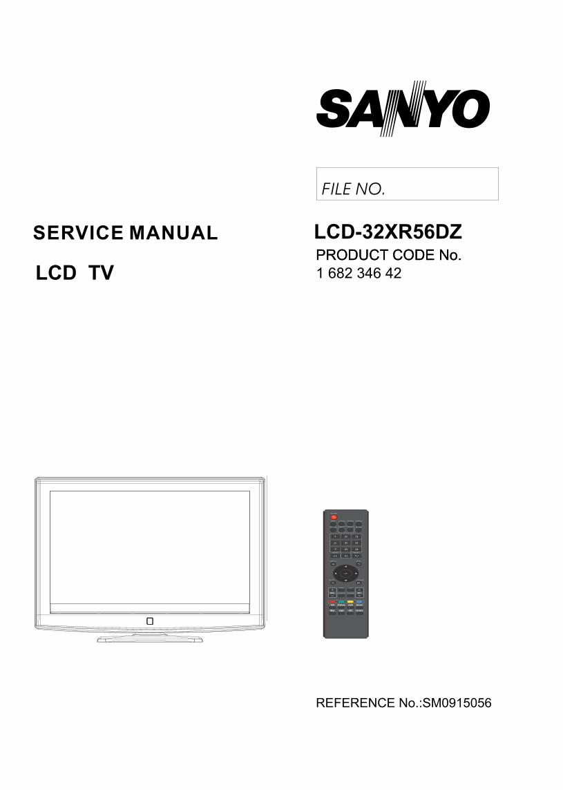
3 6 2 LCD TV
LCD-32XR56DZ
CONTENTS
Safety precautions………………………………………………………………………..…
Alignment instructions …………………………….…….…………………………………
Method of software upgrading……………………………………………………………..
Working principle analysis of the unit……………………………….………….………….
Block diagram…………………………………..………………………………….…………
IC block diagram and instruction…………………………………………………………..……
Wiring diagram …………………………………………………………………………….
Troubleshooting guide ………………………………………………………………..……
Schematic diagram…………………………………………………………………………
APPENDIX-A: Main assembly list
APPENDIX-B: Exploded View
3
5
11
15
18
19
23
24
27
Safety precautions 1. Instructions Be sure to switch off the power supply before replacing or welding any components or inserting/plugging in connection wire Anti static measures to be taken (throughout the entire production process!): a) Do not touch here and there by hand at will; b) Be sure to use anti static electric iron; c) It’s a must for the welder to wear anti static gloves. Please refer to the detailed list before replacing components that have special safety requirements. Do not change the specs and type at will. 2. Points for attention in servicing of LCD 2.1 Screens are different from one model to another and therefore not interchangeable. Be sure to use the screen of the original model for replacement. 2.2 The operation voltage of LCD screen is 700-825V. Be sure to take proper measures in protecting yourself and the machine when testing the system in the course of normal operation or right after the power is switched off. Please do not touch the circuit or the metal part of the module that is in operation mode. Relevant operation is possible only one minute after the power is switched off. 2.3 Do not use any adapter that is not identical with the TV set. Otherwise it will cause fire or damage to the set. 2.4 Never operate the set or do any installation work in bad environment such as wet bathroom, laundry, kitchen, or nearby fire source, heating equipment and devices or exposure to sunlight etc. Otherwise bad effect will result. 2.5 If any foreign substance such as water, liquid, metal slices or other matters happens to fall into the module, be sure to cut the power off immediately and do not move anything on the module lest it should cause fire or electric shock due to contact with the high voltage or short circuit. 2.6 Should there be smoke, abnormal smell or sound from the module, please shut the power off at once. Likewise, if the screen is not working after the power is on or in the course of operation, the power must be cut off immediately and no more operation is allowed under the same condition. 2.7 Do not pull out or plug in the connection wire when the module is in operation or just after the power is off because in this case relatively high voltage still remains in the capacitor of the driving circuit. Please wait at least one minute before the pulling out or plugging in the connection wire. 2.8 When operating or installing LCD please don’t subject the LCD components to bending, twisting or extrusion, collision lest mishap should result. 2.9 As most of the circuitry in LCD TV set is composed of CMOS integrated circuits, it’s necessary to pay attention to anti statics. Before servicing LCD TV make sure to take anti static measure and ensure full grounding for all the parts that have to be grounded. 2.10 There are lots of connection wires between parts behind the LCD screen. When servicing or moving the set please take care not to touch or scratch them. Once they are damaged the screen
Attention: This service manual is only for service personnel to take reference with. Before servicing please read the following points carefully.
would be unable to work and no way to get it repaired. If the connection wires, connections or components fixed by the thermotropic glue need to disengage when service, please soak the thermotropic glue into the alcohol and then pull them out in case of dagmage. 2.11 Special care must be taken in transporting or handling it. Exquisite shock vibration may lead to breakage of screen glass or damage to driving circuit. Therefore it must be packed in a strong case before the transportation or handling. 2.12 For the storage make sure to put it in a place where the environment can be controlled so as to prevent the temperature and humidity from exceeding the limits as specified in the manual. For prolonged storage, it is necessary to house it in an anti-moisture bag and put them altogether in one place. The ambient conditions are tabulated as follows:
Temperature Scope for operation 5 ~ +35 oC
Scope for storage -15~ +45 oC
Humidity Scope for operation 20% ~ 80%
Scope for storage <= 80% 2.13 Display of a fixed picture for a long time may result in appearance of picture residue on the screen, as commonly called “ghost shadow”. The extent of the residual picture varies with the maker of LCD screen. This phenomenon doesn’t represent failure. This “ghost shadow” may remain in the picture for a period of time (several minutes). But when operating it please avoid displaying still picture in high brightness for a long time. 3. Points for attention during installation 3.1 The front panel of LCD screen is of glass. When installing it please make sure to put it in place. 3.2 For service or installation it’s necessary to use specified screw lest it should damage the screen. 3.3 Be sure to take anti dust measures. Any foreign substance that happens to fall down between the screen and the glass will affect the receiving and viewing effect 3.4 When dismantling or mounting the protective partition plate that is used for anti vibration and insulation please take care to keep it in intactness so as to avoid hidden trouble. 3.5 Be sure to protect the cabinet from damage or scratch during service, dismantling or mounting.
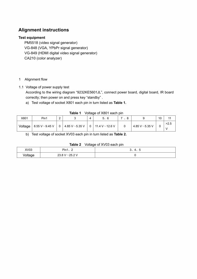
Alignment instructions Test equipment
PM5518 (video signal generator) VG-848 (VGA, YPbPr signal generator) VG-849 (HDMI digital video signal generator) CA210 (color analyzer)
1 Alignment flow
1.1 Voltage of power supply test According to the wiring diagram “9232KE5601JL”, connect power board, digital board, IR board correctly; then power on and press key “standby” . a) Test voltage of socket X801 each pin in turn listed as Table 1.
Table 1 Voltage of X801 each pin X801 Pin1 2 3 4 5、6 7 、8 9 10 11
Voltage 8.55 V~9.45 V 0 4.85 V~5.35 V 0 11.4 V~12.6 V 0 4.85 V~5.35 V 0 >2.5
V
b) Test voltage of socket XV03 each pin in turn listed as Table 2.
Table 2 Voltage of XV03 each pin XV03 Pin1、2 3、4、5
Voltage 23.8 V~25.2 V 0
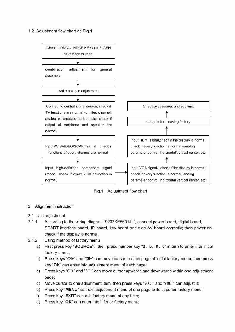
1.2 Adjustment flow chart as Fig.1
Fig.1 Adjustment flow chart
2 Alignment instruction
2.1 Unit adjustment 2.1.1 According to the wiring diagram “9232KE5601JL”, connect power board, digital board,
SCART interface board, IR board, key board and side AV board correctly; then power on, check if the display is normal.
2.1.2 Using method of factory menu a) First press key “SOURCE”,then press number key “2、5、8、0” in turn to enter into initial
factory menu; b) Press keys “CH+” and “CH-” can move cursor to each page of initial factory menu, then press
key “OK” can enter into adjustment menu of each page; c) Press keys “CH+” and “CH-” can move cursor upwards and downwards within one adjustment
page; d) Move cursor to one adjustment item, then press keys “VOL-” and “VOL+” can adjust it; e) Press key “MENU” can exit adjustment menu of one page to its superior factory menu; f) Press key “EXIT” can exit factory menu at any time; g) Press key “OK” can enter into inferior factory menu;
Check if DDC、、HDCP KEY and FLASH
have been burned.
combination adjustment for general
assembly
white balance adjustment
Connect to central signal source, check if
TV functions are normal -omitted channel,
analog parameters control, etc; check if
output of earphone and speaker are
normal.
Input VGA signal,check if the display is normal;
check if every function is normal -analog
parameter control, horizontal/vertical center, etc.
Input AV/SVIDEO/SCART signal,check if
functions of every channel are normal.
Input HDMI signal,check if the display is normal;
check if every function is normal –analog
parameter control, horizontal/vertical center, etc.
setup before leaving factory
Check accessories and packing.
Input high-definition component signal
(mode), check if every YPbPr function is
normal.
h) Factory menu item “ADC Calibrate” is used to correct ADC of VGA and Component channel;
i) Factory menu item “W/B ADJUST” is used to adjust white balance; j) Factory menu item “POWER MODE” is used to set power-on mode, “Standby” means the
set will be in standby state after power-on; “MEM” means the set will be in the state before the last power-off; “ForceOn” means the set will be working automatically after power-on, this mode is also used for factory-machine-aging; default setting should be “Standby” mode unless specified by customer requirement;
k) Factory menu item “ISP MODE” is used to upgrade unit software from VGA port when the item is set as “ON” and the set is connected to ISP adjustment equipment; DDC function of VGA port will be recovered when the item is set as “OFF”; the value of the item can not be kept in the memory, that is to say the item is reset as “OFF” after power-on again;
l) Factory menu item “RESET ALL” is used to reset factory menu data and user menu data; after execute the item, the set will be started up again and the startup guided picture will be displayed;
m) Factory menu item “FACTORY CHANNEL PRESET” is used to preset factory programs data; it is necessary to connect to central signal source for DTV searching programs. Now digital frequency of central signal CH28(529.5 MHz) and CH33(564.5 MHz) are distributed to Australia programs. Primary preset programs would not be modified along with the changing of central signals, so please select item DTV in menu Channel to manual search digital programs, the process will spend about 15s;
n) Factory menu item “CUSTOM CHANNEL PRESET” : first delete all DTV/ATV programs for factory adjustment, then preset ATV channel data according to customer order requirements; please execute the item to clear out all programs for factory adjustment before leaving factory;
o) Factory menu item “MST Debug” :default setting “OFF” is used for engineering models whose RS232 functions can measure up to design specifications; setting “ON” is convenient for debugging by developing tools; the value of the item can not be kept in the memory, that is to say the item is reset as “OFF” after power-on again;
p) Factory menu item “BACKLIGHT” is used to adjust backlight brightness, adjust the item and test voltage of X802-2# (PWM) to measure up to the maximum PWM voltage in panel specification;
q) Factory menu item “SSC ADJUST” is used to adjust expended functions of frequency content, the software having been preset according to model need not be adjusted again;
r) Factory menu item “AUDIO Curve” is used to adjust audio curve; without special customer requirements, the software having been preset according to model need not be adjusted again; If the software has been upgraded or EEPROM has data already, please execute item “RESET ALL” before adjustment for the first time.
2.1.3 ADC calibrationADC calibration of VGA channel
a) Switch to VGA channel; b) Press key “SOURCE”, then press number keys “2、5、8、0” to enter into initial factory menu; c) Move cursor to item “ADC ADJUST” and press key “OK” to enter into interior factory menu; d) Input VGA signal (VG-848 Timing:856(1024×768/60 Hz),Pattern 920 Gray 8 step(H)),
move cursor to item “MODE”,press keys “” and “” to select item “RGB”, then move cursor to item “AUTO ADC” and press key “OK” to begin adjustment automatically until adjustment completion. ADC calibration of YPbPr channel
a) Switch to YPbPr channel; b) Press key “SOURCE”,then press number keys “2、5、8、0” to enter into initial factory menu; c) Move cursor to item “ADC ADJUST” and press key “OK” to enter into interior factory menu; d) Input YPbPr signal (VG848 Timing 972(1080i),Pattern 918 SMPTE Color Bar), move
cursor to item “MODE”,press keys “” and “” to select item “YPbPr(HD)”, then move cursor to item “AUTO ADC” and press key “ENTER” to begin adjustment automatically, a prompt “success” displayed under “AUTO ADC” means auto-adjustment completed successfully;
e) Input YPbPr signal (VG848 Timing 978(483P),Pattern 918 SMPTE Color Bar), move cursor to item “MODE”,press keys “” and “” to select item “YPbPr(SD)”, then move cursor to item “AUTO ADC” and press key “ENTER” to begin adjustment automatically, a prompt “success” displayed under “AUTO ADC” means auto-adjustment completed successfully;
2.2 White balance adjustment Unless specified by customer, default COOL color temperature is 12000K, chromaticity coordinates is (272、278) ; default Normal color temperature is 9300K, chromaticity coordinates is(285、293); default Warm color temperature is 6500K, chromaticity coordinates is (313、329).
2.3 White balance adjustment processes The set should be working above 30 minutes before white balance adjustment for it would be in a stabler state. Use white balance apparatus CA-210 and switch to its BBY channel.
a) Switch to HDMI channel; b) Press key “SOURCE”, then press number keys “2、5、8、0” in turn to enter into initial factory
menu; c) Move to item “W/B ADJUST” and press key “OK” to enter into interior factory menu; d) Input DVI/HDMI signal (VG-848 Timing: 856(1024×768/60 Hz),Pattern:921 16 step
Gray), move cursor to item “MODE”, press keys “” and “” to select item “HDMI1” or other HDMI channels, then move cursor to item “TEMPERTURE”, press keys “” and “” to select item “COOL”;
e) Adjust items “R GAIN、G GAIN、B GAIN” to set chromaticity coordinates of the 14th step is (272、278);
f) Adjust item “R Offset、G Offset、B Offset” to set chromaticity coordinates of the 4th step is (272、278);
g) During adjustment , make sure that color temperature of bright step is (X=272±10 Y=278±10) and color temperature of dark step is (X=272±10 Y=278±10);
h) Then move cursor to item “COPY ALL” to copy white balance data to the other channels except DTV channel;
i) Check if color temperature of HDMI NORMAL and WARM meet requirements as below: bright step: allowable error is ±10, dark step: allowable error is ±10; otherwise adjust items “R_GAIN /B_GAIN/R_OFF/B_OFF” to meet requirements and then save data;
j) Switch to other channels ATV, AV,COMPONENT and D-SUB , check if color temperature of COOL,NORMAL and WARM meet requirements; otherwise adjust them respectively with 16 step Gray signal and the same adjustment method as HDMI channel’s; exit menu “W/B ADJUST” after adjustment and the data would be saved automatically;
k) DTV channel adjustment: switch to DTV channel, input 16 step Gray signal, enter into factory menu, then begin adjustment followed by steps “e, f, g”;
l) Adjustment rules for reference as below: adjust B gun: adjust B gun value downwards , then coordinates of X、Y will rise; adjust B gun value upwards , then coordinates of X、Y will descent; adjust R gun will effect the coordinate of X , and effect the value of Lv a little: adjust R gun value upwards , then coordinate of X will rise; adjust R gun value downwards , then coordinate of X will descent; adjust G gun will effect the coordinate of Y , and effect the value of Lv a lot: adjust G gun value upwards , then coordinate of Y will rise; adjust G gun value downwards , then coordinate of Y will descent; note: default color temperature for SANYO customer is Normal; change to picture mode Dynamic, adjust chromaticity coordinates of color temperature Normal and Cool; only adjust chromaticity coordinates of color temperature Cool for other customers when picture mode is Dynamic.
3 Performance check
3.1 TV functions Connect RF port to central signal source, first enter into menu CHANNEL, then search programs automatically, check if there is any omitted program, check if the output of speakers is normal, check if the picture is normal.
3.2 AV/S-Video port Input AV/S-Video signal respectively, check if the picture, the sound and other functions are normal;
3.3 SCART port Input signal to SCART port, check if the picture, the sound and other functions are normal; Switch to TV channel, check if the picture, the sound and other functions of SCART OUT channel are normal;
3.4 YPbPr/YCbCr port Input YUV signal from signal generator VG-848 with YUV formats as Table 4 respectively, check if the display and the sound are normal under the circumstances of power-on/off, switching channel, switching signal format, etc.
Table 4 YUV receiving signal formats
No. Definition
Horizontal
frequency (kHz)
Vertical frequenvy(Hz)
Dot-pulse
frequency (MHz)
Remark
1 720×480 15.734 60 13.5 480i (NTSC)
2 720×480 15.734 59.94 13.5 480i (NTSC)
3 720×576 15.625 50 13.5 576i (PAL)
4 720×480 31.469 60 27 480p (NTSC
PROG)
5 720×480 31.469 59.94 27 480p (NTSC
PROG)
6 720×576 31.25 50 27 576p (PAL PROG)
7 1280×720 45 59.94 74.18 720p (59p)
8 1280×720 45 60 74.25 720p (60p)
9 1280×720 37.5 50 74.25 720p (50p)
10 1920×1080 33.75 59.94 74.25 1080i (59i)
11 1920×1080 33.75 60 74.25 1080i (60i)
12 1920×1080 28.125 50 74.25 1080i (50i)
13 1920×1080 67.5 59.94 148.35 1080p (59p)
14 1920×1080 67.5 60 148.5 1080p (60p)
15 1920×1080 56.25 50 148.5 1080p (50p)
16 1920×1080 - 23.94/24 - -
17 1920×1080 - 25 - -
18 1920×1080 - 29.97/30 - -
3.5 VGA port Input VGA signal from signal generator VG-848 with VGA formats as Table 5 respectively, check if the display and the sound are normal; if there is any deviation of line or field, enter into main menu, select and execute items “Picture->Screen->Auto Adjusting” in turn to correct them automatically.
Table 5 VGA receiving signal formats
No. Definition
Horizontal
frequency (kHz)
Vertical
frequenvy(Hz)
Dot-pulse
frequency (MHz)
Remark
1 640×480 31.469 59.94 25.175 IBM
2 720×400 31.469 70.086 28.322 IBM
3 640×480 37.861 72.809 31.5 VESA
4 640×480 37.5 75 31.5 VESA
5 800×600 35.156 56.25 36 VESA
6 800×600 37.879 60.317 40 VESA
7 800×600 48.077 72.188 50 VESA
8 800×600 46.875 75 49.5 VESA
9 1024×768 48.363 60.004 65 VESA
10 1024×768 56.476 70.069 75 VESA
11 1024×768 60.023 75.029 78.75 VESA
12 1152×864 67.5 75 108 VESA
13 1280×960 60 60 108 VESA
14 1280×1024 63.98 60.02 108 VESA
15 1280×1024 80 75 135 SXGA
16 1440×900 - 60 - -
17 1680×1050 - 60 - -
18 1360×768 47.7 60 85.5 -
3.6 HDMI port Input HDMI signal from signal generator VG-849 with the formats as Table 4 and Table 5 respectively, check if the display and the sound(32 KHz、44.1 KHz、48 KHz)are normal under the circumstances of power-on/off, switching channel, switching signal format, etc.
3.7 Other functions check a) Check if the functions are normal —timing turn-on/off、 turn-off of sleeping time、
picture/sound mode、OSD、stereo and digital audio interface, etc.; b) Check if audio only digital programs (RADIO) are normal; c) For UK models, check if MHEG function of digital programs are normal; d) Check if common interface(CI:Common Interface)is normal; e) For New Zealand models, check if function of logic channel number (LCN) is normal, check
if function of Over Air Download(OAD)is normal; f) For France, UK and Italy models, check if function of logic channel number (LCN) is
normal.
4 User menu setup before leaving factory
Enter into page “LOCK” of user menu, select submenu item “Restore Factory Default” to preset items before leaving factory as below: a) Clear out all programs information; b) Clear out information of parental control (VCHIP); c) Default setup of user analog data; d) Set Menu Language as English; e) Set Power on MODE as Off.
5 Instruction of factory software burning as Table 6
Table 6 Instruction of factory software burning
No. Part No. Part type
Instruction of
software
function
Burned
before
SMT
Burning method
N111 5276405001 MX25L6405DMI-12G FLASH Yes
burned with program
ALL100, write-protect setup,
refer to Note 1 in detail
N108 5272404002 AT24C04 HDMI KEY Yes burned with program ALL100
NA04 5272402002 AT24C02 HDMI EDID Yes burned with program ALL100
NA05 5272402002 AT24C02 HDMI EDID Yes burned with program ALL100
NA06 5272402002 AT24C02
HDMI EDID
(supporting
the3rd HDMI)
Yes burned with program ALL100
N106 5272402002 AT24C02 VGA EDID Yes burned with program ALL100
Note 1: Write-protect setup method Enter into burning interface of program ALL-100, select item “Config”, press item “config Setting”, set item “Protect” as “All Protect”; be sure to select item “Config” before burning software, and write-protect must be re-set after burning program ALL-100 startup every time.
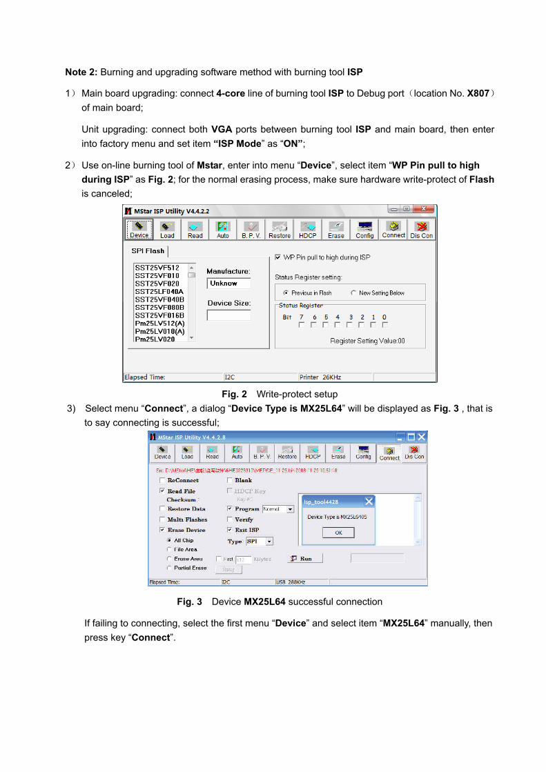
Note 2: Burning and upgrading software method with burning tool ISP
1) Main board upgrading: connect 4-core line of burning tool ISP to Debug port(location No. X807)of main board;
Unit upgrading: connect both VGA ports between burning tool ISP and main board, then enter into factory menu and set item “ISP Mode” as “ON”;
2) Use on-line burning tool of Mstar, enter into menu “Device”, select item “WP Pin pull to high during ISP” as Fig. 2; for the normal erasing process, make sure hardware write-protect of Flash is canceled;
Fig. 2 Write-protect setup
3) Select menu “Connect”, a dialog “Device Type is MX25L64” will be displayed as Fig. 3 , that is to say connecting is successful;
Fig. 3 Device MX25L64 successful connection
If failing to connecting, select the first menu “Device” and select item “MX25L64” manually, then press key “Connect”.
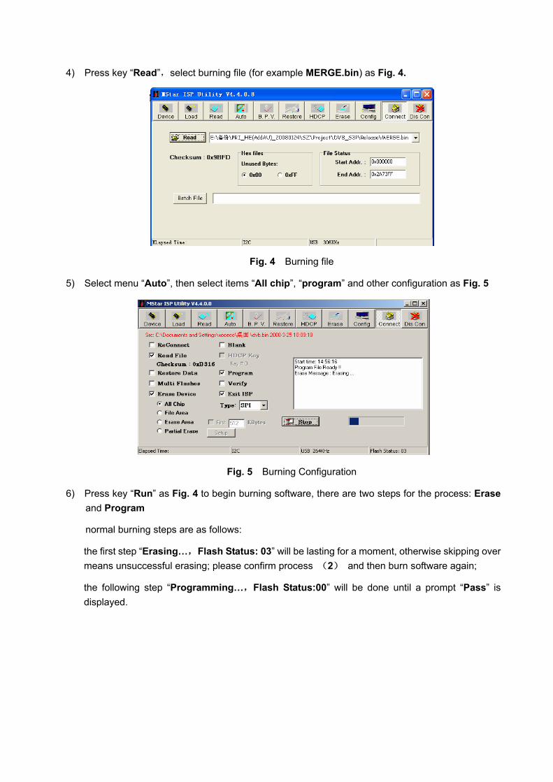
4) Press key “Read”,select burning file (for example MERGE.bin) as Fig. 4.
Fig. 4 Burning file
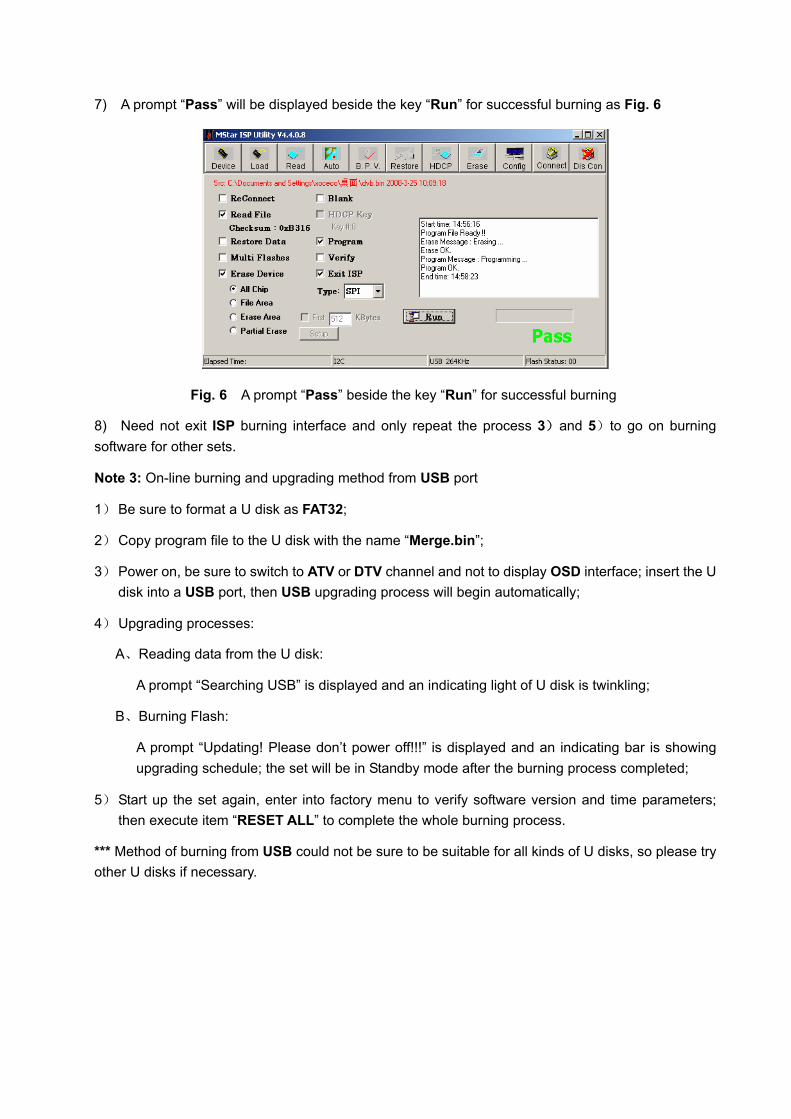
5) Select menu “Auto”, then select items “All chip”, “program” and other configuration as Fig. 5
Fig. 5 Burning Configuration
6) Press key “Run” as Fig. 4 to begin burning software, there are two steps for the process: Erase and Program
normal burning steps are as follows:
the first step “Erasing…, Flash Status: 03” will be lasting for a moment, otherwise skipping over means unsuccessful erasing; please confirm process (2) and then burn software again;
the following step “Programming…,Flash Status:00” will be done until a prompt “Pass” is displayed.
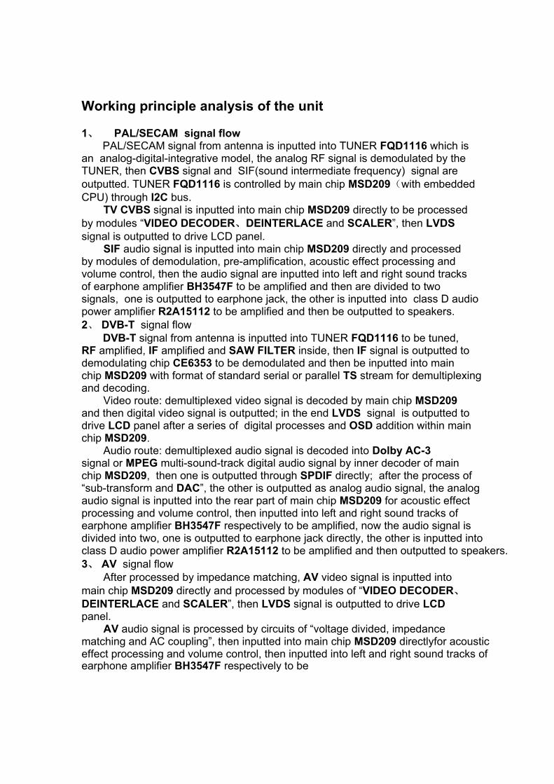
7) A prompt “Pass” will be displayed beside the key “Run” for successful burning as Fig. 6
Fig. 6 A prompt “Pass” beside the key “Run” for successful burning
8) Need not exit ISP burning interface and only repeat the process 3)and 5)to go on burning software for other sets.
Note 3: On-line burning and upgrading method from USB port
1) Be sure to format a U disk as FAT32;
2) Copy program file to the U disk with the name “Merge.bin”;
3) Power on, be sure to switch to ATV or DTV channel and not to display OSD interface; insert the U disk into a USB port, then USB upgrading process will begin automatically;
4) Upgrading processes:
A、Reading data from the U disk:
A prompt “Searching USB” is displayed and an indicating light of U disk is twinkling;
B、Burning Flash:
A prompt “Updating! Please don’t power off!!!” is displayed and an indicating bar is showing upgrading schedule; the set will be in Standby mode after the burning process completed;
5) Start up the set again, enter into factory menu to verify software version and time parameters; then execute item “RESET ALL” to complete the whole burning process.
*** Method of burning from USB could not be sure to be suitable for all kinds of U disks, so please try other U disks if necessary.
Working principle analysis of the unit 1、 PAL/SECAM signal flow PAL/SECAM signal from antenna is inputted into TUNER FQD1116 which is an analog-digital-integrative model, the analog RF signal is demodulated by the TUNER, then CVBS signal and SIF(sound intermediate frequency) signal are outputted. TUNER FQD1116 is controlled by main chip MSD209(with embeddedCPU) through I2C bus.
TV CVBS signal is inputted into main chip MSD209 directly to be processed by modules “VIDEO DECODER、DEINTERLACE and SCALER”, then LVDS signal is outputted to drive LCD panel.
SIF audio signal is inputted into main chip MSD209 directly and processed by modules of demodulation, pre-amplification, acoustic effect processing and volume control, then the audio signal are inputted into left and right sound tracks of earphone amplifier BH3547F to be amplified and then are divided to two signals, one is outputted to earphone jack, the other is inputted into class D audiopower amplifier R2A15112 to be amplified and then be outputted to speakers. 2、 DVB-T signal flow
DVB-T signal from antenna is inputted into TUNER FQD1116 to be tuned, RF amplified, IF amplified and SAW FILTER inside, then IF signal is outputted to demodulating chip CE6353 to be demodulated and then be inputted into main chip MSD209 with format of standard serial or parallel TS stream for demultiplexingand decoding.
Video route: demultiplexed video signal is decoded by main chip MSD209 and then digital video signal is outputted; in the end LVDS signal is outputted to drive LCD panel after a series of digital processes and OSD addition within main chip MSD209.
Audio route: demultiplexed audio signal is decoded into Dolby AC-3 signal or MPEG multi-sound-track digital audio signal by inner decoder of main chip MSD209, then one is outputted through SPDIF directly; after the process of “sub-transform and DAC”, the other is outputted as analog audio signal, the analog audio signal is inputted into the rear part of main chip MSD209 for acoustic effect processing and volume control, then inputted into left and right sound tracks of earphone amplifier BH3547F respectively to be amplified, now the audio signal is divided into two, one is outputted to earphone jack directly, the other is inputted into class D audio power amplifier R2A15112 to be amplified and then outputted to speakers. 3、 AV signal flow
After processed by impedance matching, AV video signal is inputted into main chip MSD209 directly and processed by modules of “VIDEO DECODER、DEINTERLACE and SCALER”, then LVDS signal is outputted to drive LCD panel.
AV audio signal is processed by circuits of “voltage divided, impedance matching and AC coupling”, then inputted into main chip MSD209 directlyfor acoustic effect processing and volume control, then inputted into left and right sound tracks of earphone amplifier BH3547F respectively to be
amplified, now the audio signal is divided into two, one is outputted to earphone jack directly, the other is inputted into class D audio power amplifier R2A15112 to be amplified and then outputted to speakers. 4、 PC/YPbPr signal flow
After processed by impedance matching, PC/YPbPr video signal is inputted into main chip MSD209 to be processed by modules of “A/D transform, digital video processing and OSD addition”, then LVDS signal is outputted to drive LCD panel.
PC/YPbPr audio signal is processed by circuits of “voltage divided, impedance matching and AC coupling”, then inputted into main chip MSD209 directly for acoustic effect processing and volume control, afterwards the audio signal is inputted into left and right sound tracks of earphone amplifier BH3547F directly to be amplified, now the audio signal is divided into two, one is outputted to earphone jack directly, the other is inputted into class D audio power amplifier R2A15112 to be amplified and then outputted to speakers. 5、 HDMI signal flow
HDMI video signal is inputted into main chip MSD209 to be processed by modules of “digital video processing and OSD addition”, then LVDS signal is outputted to drive LCD panel. HDMI audio signal is decoded into Dolby AC-3 signal or MPEG multi-sound-track digital audio signal by inner decoder of main chip MSD209, then one is outputted through SPDIF directly; after the process of “sub-transform and DAC”, the other is outputted as analog audio signal, the analog audio signal is inputted into the rear part of main chip MSD209 for acoustic effect processing and volume control, then inputted into left and right sound tracks of earphone amplifier BH3547F respectively to be amplified, now the audio signal is divided into two, one is outputted to earphone jack directly, the other is inputted into class D audio power amplifier R2A15112 to be amplified and then outputted to speakers. 6、 Brief instruction on unit functions MPEG-2 MP@HL、H.264 Main and High profile up to Leve4.0 Decoding MPEG、Dolby Digital(AC-3)、AAC Digital Audio Decoding 3D comb filter Wide-range power supply、low consumed power in standby mode(≤1W) Class D audio power amplifier with HI-FI acoustic effect output High quality transformation from interleaved scanning to progressive scanning
Realizing integrative functions really - build integration - integrative TUNER(integrating analog with digital) - integrative searching-program function - integrative OSD interface
Main parts of the unit: 32 inch LCD panel(1366X768)
Main chip:MStar MSD209FG-LF Demodulating chip:Intel CE6353 TUNER:NXP FQD1116ME/IV DDR:SAMSUNG K4T51163QC-HCF7 Class D audio power amplifier:RENESAS R2A15112
FLASH :MX25L6405DMI-12G External ports of the unit:
Two groups of Video input and RCA L/R input One group of S-VIDEO input Two groups of HDMI input One group of VGA input One group of audio input for VGA and DVI(Mini Phone Jack) One group of YPBPR input and RCA L/R input One group of RF One group of RS232(Mini Phone Jack) One group of audio output(Mini Phone Jack) One group of Video output and RCA L/R output One group of SPDIF(coaxial)output One group of USB(for upgrading)
Block diagram
IC block diagram and instruction
1、 Main chip MSD209FG-LF: GENERAL DESCRIPTION
The MSD209FG is a highly integrated controller IC for LCD/PDP DTV applications with resolutions up to full-HD (1920 x 1080). It is configured with an integrated triple-ADC/PLL, a multi-standard TV video and audio decoder, a motion adaptive video de-interlacer, a scaling engine, the MStarACE-3 color engine, an advanced 2D graphics engine, a transport processor, a high-definition (HD) MPEG video decoder, a 24-bit DSP for MPEG audio decoding, a DVI/HDCP/HDMI receiver, and a peripheral control unit providing a variety of HDTV control functions. For digital TV application, the MSD209FG comprises an MPEG-2 transport processor with advanced section filtering capability, an MPEG-2 (MP@HL profile) video decoder, an MPEG layer I and II digital audio decoder with analog audio outputs that are designed to support existing and future DVB-T programs while handling conditional access. Furthermore, it is also possible to decode MPEG-4, JPEG, MP3 formats from external sources such as USB interfaces. For analog TV, the MSD209FG includes NTSC/PAL/SECAM multi-standard video decoder comprising a 3-D motion adaptive comb filter and time-based correction, and a NICAM/A2 audio decoder to support worldwide television standards. The MSD209FG is also configured with a VBI processor to decode digital information such as Close Caption / V-chip / teletext / WSS / CGMS-A / VPS. In addition, the MStar advanced LCD TV processor enhances video quality, motion adaptive de-interlacer, picture quality adjustment units, and MStarACE-3 color engine. By integrating peripherals including two USB 2.0 host controllers, UARTs, IR, SPI, I2C, and PWM, the MSD209FG fulfills all requirements in advanced DTV sets. To further reduce system costs, the MSD209FG also integrates intelligent power management control capability for green-mode requirements and spread-spectrum support for EMI management.
MSD209FG Features: Analog RGB Compliant Input Ports
Three analog ports support up to 1080P Supports PC RGB input up to SXGA@75Hz Supports HDTV RGB/YPbPr/YCbCr Supports Composite Sync and SOG (Sync-on-Green) separator Automatic color calibration VIF Input Support
Multi-standard analog TV receiver applications Digital low IF architecture
Stepped-gain PGA with 25 dB tuning range and 1 dB tuning resolution Maximum IF gain of 37 dB Programmable TOP to accommodate different tuner gain to optimize noise and linearity performance DVI/HDCP/HDMI Compliant Input Port
Three DVI/HDCP/HDMI input ports support up to 225MHz @ 1080P 60Hz with 12-bit deep-color resolution Single link on-chip DVI 1.0 compliant receiver High-bandwidth Digital Content Protection (HDCP) 1.1 compliant receiver High Definition Multimedia Interface (HDMI) 1.3 compliant receiver with CEC (Consumer Electronics Control) support Long-cable tolerant robust receiving High -Performance Scaling Engine
Fully Programmable shrink/zoom capabilities Nonlinear video scaling supports various modes including Panorama Auto -Configuration/Auto-Detection
Auto input signal format and mode detection Auto-tuning function including phasing, positioning, offset, gain, and jitter detection Sync Detection for H/V Sync Video Processing & Conversion
3-D motion adaptive video de-interlacers with edge-oriented adaptive algorithm for smooth low-angle edges Automatic 3:2 pull-down & 2:2 pull-down detection and recovery MStar 3rd Generation Advanced Color Engine (MStarACE-3) automatic picture enhancement gives: Brilliant and fresh color Intensified contrast and details Vivid skin tone Sharp edge Enhanced depth of field perception Accurate and independent color control sRGB compliance allows end-user to experience the same colors as viewed on CRTs and other displays 10-bit internal data processing Programmable 12-bit RGB gamma CLUT 3-D video noise reduction MPEG artifact removal including de-blocking and mosquito noise reduction Frame rate conversion MFC (Motion Frame Conversion) supports: Judder-free motion video Output frame rate 50/60/100/120 f/sec Up to 60Hz full HD or 120Hz HD panels Output Interface
Supports up to 10-bit dual LVDS full-HD (1920 x 1080) panel interface Supports 2 data output formats: Thine & TI data mappings Compatible with TIA/EIA With 6/8 bits optional dithered output Spread spectrum output frequency for EMI suppression CVBS Video Output
Supports two CVBS bypass output ports 2D Graphics Engine
Point draw, line draw, rectangle draw/fill and text draw BitBlt and stretch BitBlt Raster Operation (ROP) Miscellaneous
DRAM controller to support up to 32-bit DDR2 interface Supports Common Interface for conditional access SPI bus for external flash Two ports of USB 2.0 host controller with the flexibility for connecting external storage devices 375-ball LFBGA package Operating at 1.26V (core), 1.9V (DDR2), and 3.3V (I/O and analog)
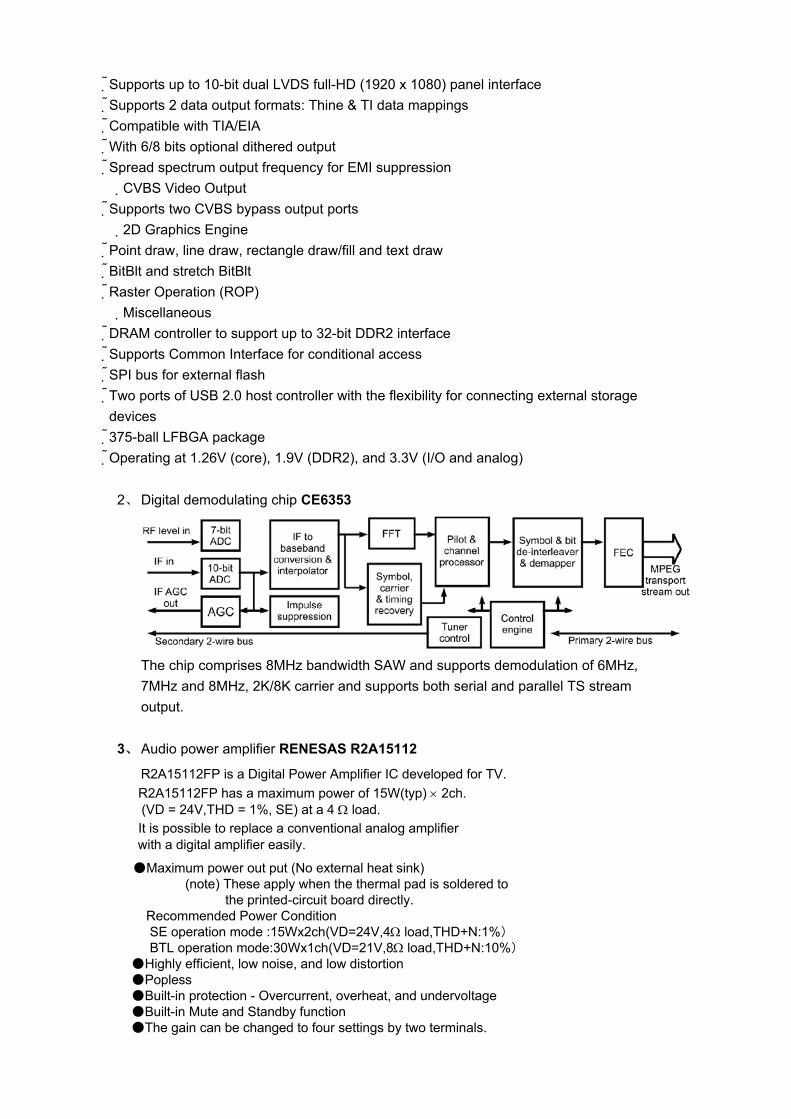
2、 Digital demodulating chip CE6353
The chip comprises 8MHz bandwidth SAW and supports demodulation of 6MHz, 7MHz and 8MHz, 2K/8K carrier and supports both serial and parallel TS stream output.
3、 Audio power amplifier RENESAS R2A15112
R2A15112FP is a Digital Power Amplifier IC developed for TV. R2A15112FP has a maximum power of 15W(typ) × 2ch.
(VD = 24V,THD = 1%, SE) at a 4 Ω load. It is possible to replace a conventional analog amplifier
with a digital amplifier easily.
Maximum power out put (No external heat sink) (note) These apply when the thermal pad is soldered to
the printed-circuit board directly. Recommended Power Condition SE operation mode :15Wx2ch(VD=24V,4Ω load,THD+N:1%) BTL operation mode:30Wx1ch(VD=21V,8Ω load,THD+N:10%)
Highly efficient, low noise, and low distortion PoplessBuilt-in protection - Overcurrent, overheat, and undervoltageBuilt-in Mute and Standby functionThe gain can be changed to four settings by two terminals.
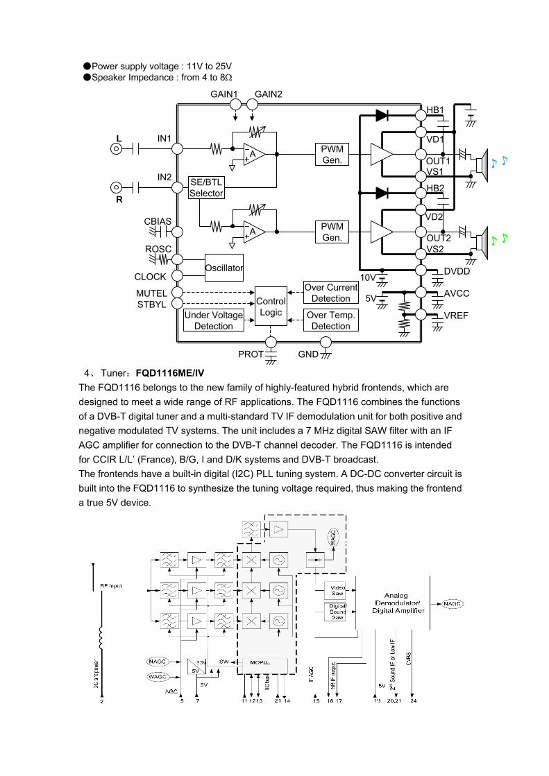
4、 Tuner:FQD1116ME/IV The FQD1116 belongs to the new family of highly-featured hybrid frontends, which are designed to meet a wide range of RF applications. The FQD1116 combines the functions of a DVB-T digital tuner and a multi-standard TV IF demodulation unit for both positive and negative modulated TV systems. The unit includes a 7 MHz digital SAW filter with an IF AGC amplifier for connection to the DVB-T channel decoder. The FQD1116 is intended for CCIR L/L’ (France), B/G, I and D/K systems and DVB-T broadcast. The frontends have a built-in digital (I2C) PLL tuning system. A DC-DC converter circuit is built into the FQD1116 to synthesize the tuning voltage required, thus making the frontend a true 5V device.
Power supply voltage : 11V to 25V Speaker Impedance : from 4 to 8Ω
Under VoltageDetection
Over Temp.Detection
Over CurrentDetectionControl
LogicSTBYL
GND
IN1
A
MUTEL
PROT
CBIASA
IN2
PWMGen.
PWMGen.
Oscillator
ROSC
GAIN1 GAIN2
SE/BTLSelector
OUT1
HB1
VD1
VS1
OUT2
VD2
VS2
HB2
DVDD
AVCC
R
L
CLOCK
VREF
10V
5V
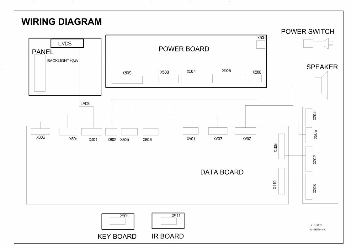
WIRING DIAGRAM
POWER BOARD
POWER SWITCH
PANEL
BACKLIGHT
DATA BOARD
KEY BOARD
IR BOARD
SPEAKER
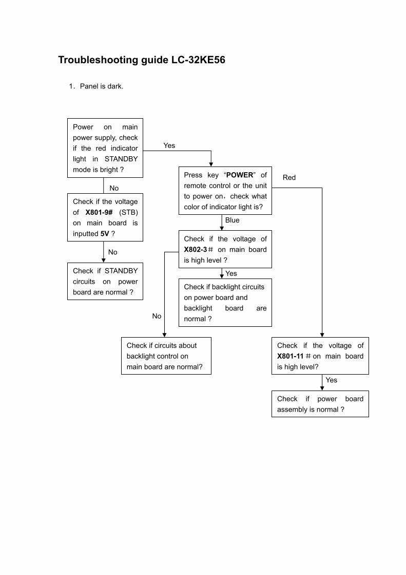
Troubleshooting guide LC-32KE56 1.Panel is dark.
Yes
Red No Blue
No Yes
No
Yes
Power on main power supply, check if the red indicator light in STANDBY mode is bright ?
Check if backlight circuits on power board and backlight board are normal ?
Check if STANDBY circuits on power board are normal ?
Press key “POWER” of remote control or the unit to power on,check what color of indicator light is?
Check if the voltage of X802-3# on main board is high level ?
Check if the voltage of X801-11#on main board is high level?
Check if power board assembly is normal ?
Check if the voltage of X801-9# (STB) on main board is inputted 5V ?
Check if circuits about backlight control on main board are normal?
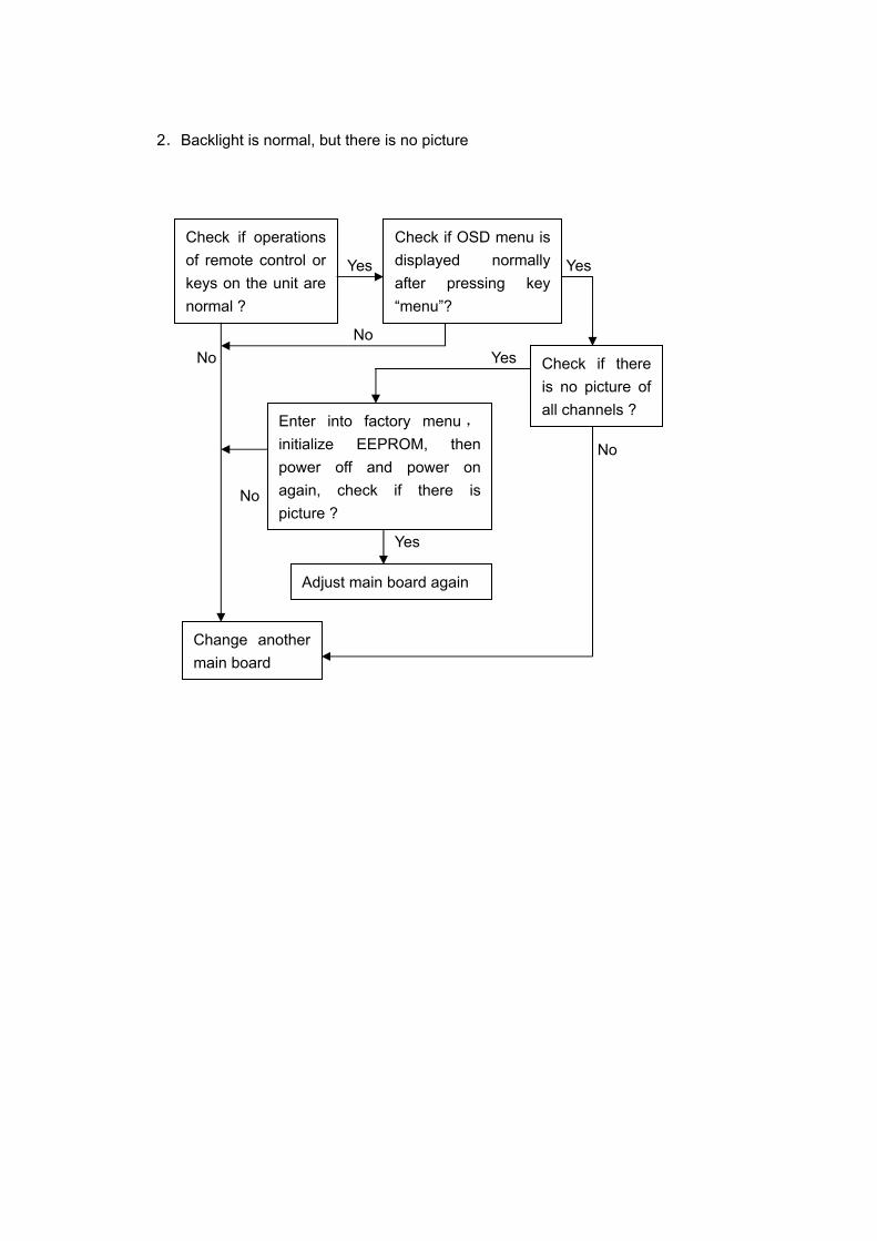
2.Backlight is normal, but there is no picture
Yes Yes No No Yes TV 有 No No
Yes
Check if operations of remote control or keys on the unit are normal ?
Check if there is no picture of all channels ?
Enter into factory menu ,
initialize EEPROM, then power off and power on again, check if there is picture ?
Change another main board
Adjust main board again
Check if OSD menu is displayed normally after pressing key “menu”?
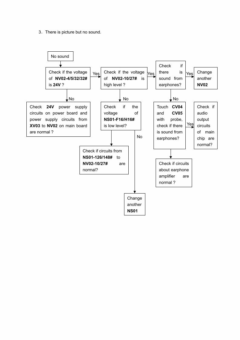
3.There is picture but no sound.
Yes Yes Yes No No No
Yes No
No sound
Check if the voltage of NV02-4/5/32/32# is 24V ?
Check 24V power supply circuits on power board and power supply circuits from XV03 to NV02 on main board are normal ?
Check if the voltage of NV02-10/27# is high level ?
Check if the voltage of NS01-F16/H16# is low level?
Change another NV02
Check if circuits from NS01-126/148# to NV02-10/27# are normal?
Touch CV04 and CV05 with probe, check if there is sound from earphones?
Check if audio output circuits of main chip are normal?
Check if there is sound from earphones?
Change another NS01
Check if circuits about earphone amplifier are normal ?
Sheet to
DRAWN BY
11
1
X1.0
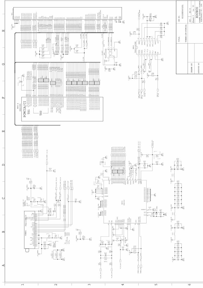
TUNER+IF+PCMCIA
9232KE5601DL
PCMCIA/CI
XOCECO
E
XIAMEN OVERSEAS CHINESE
ELECTRONIC CO., LTD.
TITLE:
DWG NO.
REV.
APPROVED BY
NJ01
CE6353
TUNER1
FDQ1116ME/IV
NM02
TPS2211AIDBR
NS01
MSD209FG
TS1
TS0
TS_MDI[2]
TS_MDI[0]
TS_MDI[4]
TS_MDI[7]
TS_MIVAL
TS_MISTRT
TS_MDI[5]
TS_MDI[3]
TS_MDI[6]
TS_MDI[1]
CI_ADDR[5]
INPACK
TS_MDI[4]
CI_WAIT#
TS_MDO[1]
TS_MOVAL
TS_MDO[2]
PCM_A[1]
CI_ADDR[4]
TS_PVAL
TS_PSTRT
TS_MDO[7]
PC_C_DETECT1#
PC_REG#
CI_DATA[0]
PCM_A[3]
PC_C_DETECT2#
CI_VS1#
TS_PD[2]
TS_PD[4]
TS_MDI[6]
PC_REG#
TS_MDO[4]
CI_CE1#
TS_MDO[5]
TS_MDO[3]
CI_CE2#
CI_ADDR[14]
CI_ADDR[0]
TS_MISTRT
PCM_A[14]
CI_ADDR[3]
TS_MOCLK
CI_DATA[2]
CI_VS1#
TS_MIVAL
TS_MDI[1]
PCM_A[7]
CI_ADDR[11]
TS_MOSTRT
TS_PD[0]
CI_ADDR[2]
CI_WE#
CI_ADDR[8]
PC_RST
PCM_A[8]
CI_ADDR[12]
PCM_A[10]
CI_CE2#
PC_C_DETECT2#
CI_DECT
CI_ADDR[1]
TS_MDI[3]
TS_MDI[0]
CI_WE#
CI_DATA[5]
PCM_A[4]
CI_ADDR[9]
PCM_A[6]
CI_ADDR[10]
PCM_D[0]
CI_IOWR#
CI_IOWR#
PCM_A[11]
TS_MDI[2]
PCM_D[2]
PCM_A[2]
TS_PD[6]
IOIS
CI_ADDR[6]
PCM_D[3]
INPACK
CI_DATA[6]
PCM_D[6]
TS_PD[7]
TS_MDI[5]
PCM_D[5]
CI_DATA[3]
TS_MDO[6]
TS_MICLK
CI_ADDR[7]
CI_IORD#
CI_OE#
PCM_A[12]
PCM_D[1]
TS_MDO[0]
PC_RST
CI_OE#
CI_WAIT#
CI_ADDR[13]
PC_C_DETECT1#
PCM_A[0]
TS_MDI[7]
TS_PD[5]
CI_IREQ#
CI_DATA[7]
PCM_D[4]
PCM_A[5]
CI_CE1#
CI_DATA[1]
PCM_A[13]
PCM_D[7]
IOIS
PCM_A[9]
CI_DATA[4]
TS_PD[3]
TS_PD[1]
CI_IORD#
CI_IREQ#
CI_CD#
PC_C_DETECT2#
PC_C_DETECT1#
TS_MOCLK
TS_MOSTRT
TS_MOVAL
TS_MDO[0]
TS_MDO[1]
TS_MDO[2]
TS_MDO[3]
TS_MDO[4]
TS_MDO[5]
TS_MDO[6]
TS_MDO[7]
CI_IORD#
CI_IOWR#
CI_OE#
CI_WE#
PC_REG#
CI_CE#
CI_IREQ#
CI_WAIT#
PC_RST
CI_ADDR[0]
CI_ADDR[1]
CI_ADDR[2]
CI_ADDR[3]
CI_ADDR[4]
CI_ADDR[5]
CI_ADDR[6]
CI_ADDR[7]
CI_ADDR[8]
CI_ADDR[9]
CI_ADDR[10]
CI_ADDR[11]
CI_ADDR[12]
CI_ADDR[13]
CI_ADDR[14]
CI_DATA[0]
CI_DATA[1]
CI_DATA[2]
CI_DATA[3]
CI_DATA[4]
CI_DATA[5]
CI_DATA[6]
CI_DATA[7]
CI_CD#
CI_CE#
TS_MICLK
TS_PCLK
TS_MDI[6]
TS_MDI[1]
TS_MIVAL
TS_MDI[0]
TS_MICLK
TS_MDI[3]
TS_MDI[5]
TS_MDI[4]
TS_MISTRT
TS_MDI[7]
TS_MDI[2]
TS_MDO[1]
TS_MDO[3]
TS_MDO[2]
TS_MDO[5]
TS_MDO[4]
TS_MDO[7]
TS_MOVAL
TS_MOCLK
TS_MOSTRT
TS_MDO[0]
TS_MDO[6]
GND-A
TUNER_SCL
L102
STBL2012-501
TS_MISTRT
TUNER_SDA
GND-A
RJ26
100
L103
STBL2012-501
RJ20
4.7K
RJ22
0
RJ17
33
+3.3V_DE
RJ24
33
GND-A
RJ071K
TS_MICLK
TS_MDI[5]
+5V
RJ27
100
RJ11
10K
RJ23
8.2K
GND-A
+1.8V_ADE
+5V
RJ044.7K
GND-A
TV_FAT_IFN
GND-D
+3.3V_DE
RST_6353
002:D4
RJ12
0
GND-A
TV_FAT_IFN
TUNER_SCL
L106
22uH
GND-D
GND-D
RJ2910K
TV_IF_AGC
RJ10
10KTV_SIFM
002:D3
GND-D
TS_MDI[4]
C101
10n
TS_MDI[3]
TS_MDI[7]
TV_FAT_IFP
CJ01
100n
RJ16
33
+3.3V_DE
TS_MDI[6]
GND-D
+3.3V_DE
CJ1015p
GND-D
CJ0815p
GND-A
TV_FAT_IFP
GND-D
TS_MIVAL
RJ15
33
CJ0633p
+3.3V_DE
TS_MDI[2]
TV_IF_AGC
RJ25
33
RJ05
10K
CJ0733p
GND-D
RJ08
2.2M
GND-D
RJ01
100
RJ034.7K
CJ09100n
RJ21
4.7K
GND-D
RJ06
1K
TV_SIFP
002:D3
RJ2810K
+3.3V_DE
RJ02
100
CJ02
100n
TS_MDI[0]
GND-D
TS_MDI[1]
SDA
007:C3
SCL
007:C3
+1.8V_DE
+1.8V_CORE
+1.8V_DE
+1.8V_PDE
CJ112.2u
GND-D
CJ124.7u
GND-D
+1.8V_ADE
+1.8V_DE
CJ134.7u
GND-D
TUNER_SDA
LJ01
LJ02
LJ03
+1.8V_CORE
CJ14100n
CJ21100n
CJ23100n
CJ15100n
CJ19100n
CJ25100n
CJ17100n
CJ18100n
CJ16100n
RJ090
GND-D
+1.8V_PDE
CJ22100n
CJ20100n
CJ24100n
GND-D
+3.3V_DE
CJ26100n
CJ27100n
R107
0
+5V_TUNER1
1Vss
2Vdd
3Vss
4CLK1
5DATA1
6IRQ
7CVdd
8Vss
9RESET
10
SLEEP
11
STATUS
12SADD4
13Vdd
14Vss
15SADD316SADD217SADD118SADD0
19CVdd
20Vss
21
PLLVdd
22
PLLGnd
23XTI
24XTO
25Vss
26
PLL1TEST
27OSCMODE
28
AVdd
29
AGnd
30
VIN
31
VIN
32
AGnd
33
Vdd33
34
RFLEV
35
CLK2/GPP0
36
DATA2/GPP1
37CVdd
38Vss
39CVdd
40Vss
41
AGC2/GPP2
42
AGC1
43
GPP3
44SMTEST
45Vdd
46Vss
47
MOSTRT
48
MOVAL
49
MDO0
50
MDO1
51
MDO2
52
MDO3
53
MDO4
54Vdd
55Vss
56
MDO5
57
MDO6
58
MDO7
59CVdd
60Vss
61
MOCLK
62
BKERR
63
MICLK
64CVdd
GJ01
20.48MHz
LJ05
39nH
1RF
2Ant_Pwr
3GND3
9GND9
10NC10
11As
4NC4
12SCL
13SDA
14REF
5RF_AGC
6GND6
7VP(TUN)
19+5V_IF
202ndIF/Low_DIF1
212ndIF/Low_DIF2
22NC
15IF_AGC
16DIF1
17DIF2
18Wout
8VT
23AS_IF
24CVBS
L101
STBL2012-501
GND-A
R101
10K
R102
10K
GND-A
GND-AR104
10K
R103
10K
XM01
PCMCIA-0070210PA8C
22
A7
1GND
21
A12
4D5
5D6
15
WE
11
A9
6D7
20
MCLK(A15)
8A10
13
A13
9OE
14
A14
17
VCC1
18
VPP1
19
MVAL(A16)
16
IREQ
7CE1
12
A8
2D3
3D4
10
A11
23
A6
24
A5
25
A4
27
A2
28
A1
26
A3
29
A0
30
D0
31
D1
32
D2
33
IOIS_16
34
GND1
35
GND2
36
CD1
37
MD3(D11)
38
MD4(D12)
39
MD5(D13)
40
MD6(D14)
41
MD7(D15)
42
CE2
43
VS1
44
IORD
45
IOWR
46
MISTRT(A17)
47
MDI0(A18)
48
MDI1(A19)
49
MDI2(A20)
50
MDI3(A21)
51
VCC2
52
VPP2
53
MDI4(A22)
54
MDI5(A23)
55
MDI6(A24)
56
MDI7(A25)
57
VS2/MCLKO
58
RESET
59
WAIT
60
INPACK
61
REG
62
MOVAL(SPKR)
63
MOSTRT(STSCHG)
64
MD0(D8)
65
MD1(D9)
66
MD2(D10)
67
CD2
68
GND3
RM25
100
CM08100n
RM35
10K
RM24
33
RM09
4.7K
RM41
0
RM2710K
CARD_SHDN#
007:B3
TS_MDI[2]
NM01
SN74LVC1G32DCKR
1A
2B
3GND
4Y
5Vcc
GND-D
RM11
100
CM021u
RM30
10K
RM33
1K
1VCCD0
2VCCD1
33.3V_3
43.3V_4
55V_5
65V_6
7GND
8OC
912V
10
AVPP
11
AVCC_11
12
AVCC_12
13
AVCC_13
14
VPPD1
15
VPPD0
16
SHDN
RM2610K
CM03
220u
10V
+3.3AVDD
RM37
10K
TS_MICLK
CM01100n
RM01
33
TS_MDI[6]
RM15
33
CM07100n
RM3910K
+VCC_CARD
TS_MIVAL
RM12
100
CARD_3.3VEN
007:B4
RM40
0
RM2910K
TS_MDI[3]
RM17
100
+3.3AVDD
+5V
GND-D
LM02
STPB2012-201PT
RM16
33
LM01
STPB2012-201PT
RM13
0
RM04
33
CM06100n
RM03
33
RM05
33
GND-D
TS_MDI[4]
+VCC_CARD
GND-D
RM02
33 +3.3AVDD
+3.3AVDD
TS_MDI[5]
RM2810K
RM34
1K
CM05100n
RM21
33
RM23
33
CI_VS1#
007:B3
+3.3AVDD
RM22
33
+VCC_CARD
CARD_5VEN
007:B4
TS_MDI[1]
RM434.7K
GND-D
RM18
100
RM32
10K
TS_MDI[7]
CI_VS1#
CARD_OC
007:B3
RM074.7K
GND-D
RM31
10K
CM04
100n
TS_MISTRT
+VCC_CARD
RM084.7K
RM14
0
RM064.7K
GND-D
+3.3AVDD
TS_MDI[0]
RM3810K
RM36
10K
+VCC_CARD
RM42
100
RM10
4.7K
+3.3AVDD
L107
SGMI2012-2R2KT
L108
SGMI2012-2R2KT
CVBS_TUNER
003:D4
C104
100uF
10V
C2142.2u
C215100n
GND-A
GND-A
C2162.2u
C217100n
N18
TS1_CLK/GPIO43
P18
TS1_SYNC/GPIO42
L17
TS1_VLD/GPIO41
M17
TS1_DO/GPIO40
Y7
TS0_CLK/GPIO39
W5
TS0_SYNC/GPIO38
V6
TS0_VLD/GPIO37
U6
TS0_D2/GPIO31
V4
TS0_D0/GPIO29
U5
TS0_D1/GPIO30
R7
TS0_D3/GPIO32
R8
TS0_D4/GPIO33
T7
TS0_D5/GPIO34
T8
TS0_D6/GPIO35
V5
TS0_D7/GPIO36
U18
PCM_IORD_N/CI_RD/GPIO87
T18
PCM_IOWR_N/CI_WR/GPIO88
V18
PCM_OE_N/GPIO89
V17
PCM_WE_N/GPIO90
U17
PCM_REG_N/CI_CLK/GPIO91
T17
PCM_CE_N/CI_CS/GPIO92
R17
PCM_IRQA_N/CI_INT/GPIO93
R18
PCM_WAIT_N/CI_WACK/GPIO94
P17
PCM_RESET/GPIO95
N17
PCM_CD_N/GPIO96
V13
PCM_A0/CI_A0/GPIO63
U13
PCM_A1/CI_A1/GPIO64
T13
PCM_A2/CI_A2/GPIO65
R13
PCM_A3/CI_A3/GPIO66
V12
PCM_A4/CI_A4/GPIO67
U12
PCM_A5/CI_A5/GPIO68
T12
PCM_A6/CI_A6/GPIO69
R12
PCM_A7/CI_A7/GPIO70
U11
PCM_A8/CI_A8/GPIO71
V9
PCM_A9/CI_A9/GPIO72
T11
PCM_A10/CI_A10/GPIO73
T10
PCM_A11/CI_A11/GPIO74
U10
PCM_A12/CI_A12/GPIO75
V8
PCM_A13/CI_A13/GPIO76
V7
PCM_A14/CI_A14/GPIO77
R11
PCM_D0/CI_D0/GPIO79
R10
PCM_D1/CI_D1/GPIO80
P9
PCM_D2/CI_D2/GPIO81
R9
PCM_D3/CI_D3/GPIO82
T9
PCM_D4/CI_D4/GPIO83
U9
PCM_D5/CI_D5/GPIO84
U8
PCM_D6/CI_D6/GPIO85
U7
PCM_D7/CI_D7/GPIO86
RJ30
220
RJ31
220
CJ3456p
RM19
100
RM20
100
CJ0322n
CJ35
10p
GND-D
CJ36
10p
GND-D
TS_MDI[0]
TS_MICLK
TS_MISTRT
TS_MIVAL
R105
330
R106
330
R279
330
R280
330
C21910p
CJ0422p
CJ0522p
GND-AC102
100uF
10V
L104
22uH
+5V
+5V_TUNER2
+5V_TUNER2
GND-A
R108120
TS_MDI[4]
TS_MDI[5]
TS_MDI[3]
TS_MISTRT
TS_MDI[2]
TS_MDI[6]
TS_MDI[0]
TS_MDI[7]
TS_MDI[1]
TS_MICLK
TS_MIVAL
RM44
33
RM45
33
RM47
33
RM46
33
RM49
33
RM48
33
RM50
33
RM51
33
RM53
33
RM52
33
RM54
33
MOPLL I2C
ADDRESS
SELECTION
SELECTION
ADDRESS
IF PART I2C
AS ADDRESS
0-0.5V C0/C1
1-1.5V/OPEN C2/C3
2-3V C4/C5
4.5-5V C6/C7
AS_IF ADDRESS
0 86/87
5V 84/85
330nH
AB
CD
EF
GH
1 2 3 4 5 6
XOCECO
Sheet to
DRAWN BY
11
2
X1.0
AUDIO IN/OUT
9232KE5601DL
B
XIAMEN OVERSEAS CHINESE
ELECTRONIC CO., LTD.
TITLE:
DWG NO.
REV.
APPROVED BY
NS01
MSD209FG
AUDIO
VGA_LIN
VGA_RIN
YUV_LIN
YUV_RIN
AV_LIN
AV_R_IN
AV_L_IN
SC2_LIN
SC2_RIN
AV_L_IN
AV_L_IN
AV_R_IN
AV_R_IN
SC1_LIN
SPDIF_OUT
AV_RIN
SC1_RIN
AV2_RIN
AV2_LIN
AV2_LIN
AV2_RIN
YUV_RIN
YUV_LIN
VGA_RIN
VGA_LIN
SC1_RIN
SC1_LIN
SC2_RIN
SC2_LIN
AV_RIN
AV_LIN
External_CVBS
GND-D
GND-D
GND-D
SC1_LOUT
C1581n
R145
4.7K
R163
100
R11147K
R1474.7K
R18047
GND-D
GND-D
+5V
AV_OUTL
R162
100
R14847
R186
10K
R159
100
C1641n
R1128.2K
SC2_ROUT
V101
MMBT3904
GND-D
GND-D
R11647
R151
100
GND-D
V106
MMBT3904
+5V
R16113K
GND-D
GND-D
GND-D
C116
47p
SC2_ROUT
C1241u
R17013K
R150
4.7K
C117
47p
VGA_HSYNC
003:C3
TV_OUTL
GND-D
C163
100n
C120
100n
C157
100n
AV_OUTL
D101
MMBD1204
SC2_LOUT
R174
10K
R1154.7K
R19647
SC1_ROUT
GND-D
C106
100n
RST_6353
001:D5
C1254.7u
R142
10K
R17113K
R16613K
GND-D
R149
4.7K
GND-D
VCC-VGA
GND-D
PRIM_AUD_OUT_L008:C4
AV_OUTR
R152
100
GND-D
R154 33
R1918.2K
TV_SIFP
001:C2
C118
100n
AV_OUTR
C119
47p
SC1_LOUT
SC1_ROUT
R19047K
PESD5V0L5UY
N103
12
345
6
GND-D
External_YIN
003:C4
L111SGMI2012M1R0KT
R109
10K
PRIM_AUD_OUT_R
008:C5
R14347K
R140
33
X108
TJC10-12A
1 2 3 4 5 6 7 8 9 10
11
12
V102
MMBT3904
C160
47p
External_CIN
003:C4
R15613K
TV_OUTR
R1778.2K
GND-D
TV_OUTL
C113
100n
GND-D
C136
100n
+9V
R155 33
PESD5V0L4UG
N105
1
2
34
5
GND-D
R1448.2K
C144
100n
SC2_LOUT
R135
75
VGA_VSYNC
003:C3
GND-D
C114
47p
GND-D
R146
0
C1151n
R17647K
GND-D
GND-D
R123
75
GND-D
C108
100n
TV_OUT
003:F4
C1261n
V107
MMBT3904
GND-D
C123
100n
C128100n
R1794.7K
GND-D
R1954.7K
GND-D
GND-D
TV_SIFM
001:C2
X107
AV3-14WKD
2R_OUT 2L-OUT
2R_IN GND-D
GND-D
@pinCo
TV_OUTR
X105
JY-3541L-01-030
GRL
N106
24LC21A/SN
1NC1
2NC2
3NC3
4VSS
5SDA
6SCL
7VCLK
8VCC
C159
47p
GND-D
GND-D
R17313K
R141
33
GND-D
GND-D
C145
100n
R158
100
X103
AV205-1
WR
LR
R172
10K
PESD5V0L5UY
N104
123
4 5 6
R136
0
R134
0
C122
2.2u
C162
2.2uC109
2.2u
C156
2.2u
R12112K
R13712K
R113
10K
R114
10K R118
10K
R117
10K
R12512K
R12412K
R184
10K
R185
10K
R18212K
R18312K
R19212K
R18712K
R197
10K
R198
10K
GND-D
R18812K
R19312K
R200
10K
R199
10K
GND-D
L109
BG2012D151T
L110
BG2012D151T
L113
BG2012D151T
L112
BG2012D151T
C151
2.2u
C154
2.2u
C153
2.2u
C152
2.2u
C129
2.2n
C147
2.2n
C148
2.2n
C138
2.2n
C150
2.2n
C146
2.2n
+9V
+9V
+9V
X106
HJR-03A-OR
C149
100n
R178120
ISP_EN
V103
BC847AW
V104
BC847AW
V105
BC847AWR167
10K
R160
33
R169
33
TXD_UPDATE
007:F2
RXD_UPDATE
007:F2
R139100K
R157100K
R181100K
R203100K
R175
200
R168
200
C1074.7u
16V
C1614.7u
16V
C1554.7u
16V
C1214.7u
16V
Z107
10MHz
Z108
10MHz
Z112
10MHz
Z115
10MHz
Z106
10MHz
Z109
10MHz
Z113
10MHz
Z104
10MHz
Z105
10MHz
GND-D
GND-D
GND-D
Z111
10MHz
+3.3VDD
C13010u
MUTE_AMP
008:C3
R153
33
SPI_CZ2
ISP_EN
STANDBY_AMP008:C1
X109
TJC10-06A
1 2 3 4 5 6
GND-D
R20475
GND-D
Z114
10MHz
R19412K
GND-D
R18912K
R201
10K
R202
10K
Z110
10MHz
AV2_VIN
R5
LINE_IN_3L
Y4
LINE_IN_2R
R4
LINE_IN_1R
R3
LINE_IN_1L
V3
LINE_OUT_1L
P6
LINE_IN_0R
E14
SPDIF_OUT/GPIO48
P5
LINE_IN_0L
T3
LINE_IN_4L
T5
LINE_IN_5L
W4
LINE_OUT_0R(DACO_R)
R6
LINE_IN_3R
T4
LINE_IN_4R
U4
LINE_OUT_1R(DACO_S)
W2
SIF_INM
Y6
LINE_OUT_0L(DACO_L)
Y2
SIF_INP
T6
LINE_IN_5R
Y3
LINE_IN_2L
W3
LINE_OUT_2R
Y5
LINE_OUT_2L
F15
SPDIF_IN/GPIO47
E11
I2S_OUT_SD/GPIO52
G16
I2S_IN_BCK/GPIO45
H16
I2S_IN_WS/GPIO44
G15
I2S_IN_SD/GPIO46
E10
I2S_OUT_MUTE/LHSYNC2/GPIO13
E16
I2S_OUT_MCK/GPIO50
F16
I2S_OUT_WS/GPIO49
E12
I2S_OUT_BCK/GPIO51
V2
AU_COM(VIM0)
N5
AUVRM
N4
AUVRP
U3
AUVAG
X101
HJK-3.5-401
GG
G
CY
SGRL
GND-D
232_TXD
007:D4
232_RXD
007:D3
External_CVBS
003:C4
C137
2.2u
C127
2.2u
C135
2.2u
C143
2.2u
C142
2.2u
C132
2.2u
C139
2.2u
C133
2.2u
C134
2.2u
C131
2.2u
C140
2.2u
C141
2.2u
+3.3VDD
MUTE_AMP
008:C3
R269
10K
R273
75
GND-D
GND-D
C110100p
Pr_INPUT
003:C3
C112100p
C105
100n
R133
0
GND-D
R128
75
Y_INPUT
003:C3
GND-D
R130
0
C111100p
PESD5V0L4UG
N102
1
2
34
5
GND-D
Pb_INPUT
003:C3
R131
75
R132
75
X102
AV3-14WD
G
@pinCo
B
@pinCo
R
@pinCo
R129
0
VGA_G_IN
003:C3
PESD5V0L5UY
N101
12
345
6
X104
HC1038-15F-3.08
12345
6789
11121314
1015
GND-DR127
75
R275
0
Z103
470MHz
VGA_B_IN
003:C3
Z102
470MHz
Z116
470MHz
Z117
470MHz
R274
0
Z101
470MHz
R276
0
VCC-VGA
GND-D
R277
0
R122
75
GND-D
VGA_R_IN
003:C3
R119
75
R278
0
R126
22K
R138
22K
GND-D
R164
470
R165
470
VCLK: 0=READ ONLY
AV2
SCART
AV1
AB
CD
EF
GH
1 2 3 4 5 6
XOCECO
CVBS0
Sheet to
DRAWN BY
11
3
X1.0
VIDEO IN/OUT
9232KE5601DL
353.24040-10
353.24512-00
A Share VCOM0
XIAMEN OVERSEAS CHINESE
ELECTRONIC CO., LTD.
TITLE:
DWG NO.
REV.
APPROVED BY
NS01
MSD209FG
24C04
24C512
HDMI
RGB
S-Video
CVBS_IN
VIF
CVBS_OUT
SCRTR2_FS
SCART1_FS
SC1_FS
SC2_FS
SCART1_R
SCART1_G
SCART1_B
SCART2_Y/CVBS
SCART2_C
SC2_VOUT
SC1_FB
SCART1_B
SCART1_G
SCART1_R
SCART2_Y/CVBS
SCART2_C
SC2_VOUT
SC1_FB
SCART1_CVBS
SCART1_CVBS
CEC_PM
R265
8.2K
GND-D
Y_INPUT
002:B5
VGA_VSYNC002:C1
R259
75
R266
8.2K
GND-D
Pb_INPUT
002:B5
Pr_INPUT
002:B5
VGA_R_IN
002:B2
External_CIN
002:B5
R263
2.2K
X110
TJC10-13A
1 2 3 4 5 6 7 8 9 10
11
12
13
VGA_G_IN
002:B2
VGA_B_IN
002:B2
R260
75R261
0
External_YIN
002:B4
R262
0
VGA_HSYNC002:C1
R229
470
R235120
R236
390
R234470
R237
75
V108
MMBT3904
GND-D
+5V
GND-D
C169
1n
R23215K
C200100n
C1992.2u
C168
2.2u
V109
MMBT3906LT1
C171
47n
C172
47n
C170
47n
R254
75
V112
BC847AW
TV_OUT
002:H3
TV_CVBS
R251
220
GND-D
+9V
C206100n
L114
BG2012D151T
GND-D
GND-D
C205100n
GND-D
R209
10
R207
10
R208
10
R212
10
C173
1n
R230
470
R210
10
C176
47n
C175
47n
R211
10
C174
47n
C188
1n
R233
470
C191
47n
C190
47n
C189
47n
R223
47
R225
47
R224
47
R226
47
R227
47
R228
47
C194
47n
C192
47n
C193
47n
GND-D
C179
47n
C180
47n
R216
10
R215
10
R213
10
R214
10
C178
47n
C177
47n
C183
47n
C182
47n
C184
47n
R218
10
R220
10
R219
10
C181
47n
R217
10
R205820
GND-D
C187100n
C165100n
GND-DC197
100n
C196
100n
C195
100n
GND-D
C166
100n
SC1_FS
007:B3
SC2_FS
007:B3
SCL_HDMI-3
SCL_HDMI-2
SCL_HDMI-1
SDA_HDMI-2
SDA_HDMI-3
SDA_HDMI-1
HDMI_CEC006:D4
HDMI-1_RX2+
HDMI-1_RX1+
HDMI-1_RX0+
HDMI-1_RX0-
HDMI-1_RX1-
HDMI-1_RX2-
HDMI-1_RXC+
HDMI-1_RXC-
HDMI-2_RX0-
HDMI-2_RX0+
HDMI-2_RX2+
HDMI-2_RXC-
HDMI-2_RX2-
HDMI-2_RX1-
HDMI-2_RX1+
HDMI-2_RXC+
HDMI-3_RXC-
HDMI-3_RX2+
HDMI-3_RX2-
HDMI-3_RX0-
HDMI-3_RX0+
HDMI-3_RXC+
HDMI-3_RX1+
HDMI-3_RX1-
HOTPLUG_HDMI-1_OUT
HOTPLUG_HDMI-2_OUT
HOTPLUG_HDMI-3_OUT
R206
390
AVDD_DM
C201100n
R243
100
N107
1AO
2A1
3A2
4GND
5SDA
6SCL
7WP
8Vcc
R24410K
GND-D
R255
10K
C202100n
GND-D
SCL
SDA
SCL
R25710K
+3.3VDD
+3.3VDD
R241
100
GND-D
N108
1AO
2A1
3A2
4GND
5SDA
6SCL
7WP
8Vcc
+3.3VDD
SDA
+3.3VDD
R2490
GND-D
R238
33
R242
100
EEP_W_EN
007:B2
GND-D
R240
100
TV_CVBS
CVBS_TUNER
001:D2
C185
47n
C186
47n
R222
10
R221
10
TV_CVBS#
TV_CVBS#
R256
0
GND-D
AV2_VIN
C203
100uF
10V
C204
100uF
10V
C208
100uF
10V
C207
100uF
10V
E3
CEC/UART_RX1
C1
RXCP1
C2
RXCN1
D1
RX0P1
D2
RX0N1
E1
RX1P1
E2
RX1N1
F1
RX2P1
F2
RX2N1
E4
DDCDB_DA
E6
DDCDB_CK
E5
HOTPLUGB
G1
RXCP0
G2
RXCN0
H1
RX0P0
H2
RX0N0
G3
DDCDA_CK
W10
RX1N2
F6
DDCDA_DA
Y10
RX1P2
K2
RX2N0
W9
RX0N2
K1
RX2P0
Y9
RX0P2
R14
DDCDC_CK
J2
RX1N0
W8
RXCN2
T14
DDCDC_DA
J1
RX1P0
Y8
RXCP2
W11
RX2N2
F4
HOTPLUGA
Y11
RX2P2
K6
VSYNC2
M7
VSYNC0
L1
RIN0M
K5
CVBS_OUT2
L7
HSYNC0
L2
RIN0P
H6
RIN1P
J4
C0(CVBS6P)
F5
REXT
M1
GIN0M
H5
GIN1P
L6
RIN2P
M2
GIN0P
H3
BIN1P
L4
GIN2P
N1
BIN0M
H4
SOGIN1
L3
BIN2P
N2
BIN0P
G8
VSYNC1
L5
SOGIN2
J5
SOGIN0
G7
HSYNC1
N15
HOTPLUGC
G4
VCLP
G5
REFP
G6
REFM
J3
Y0(CVBS4P)
K3
Y1(CVBS5P)
K4
C1(CVBS7P)
M4
CVBS1P
P1
CVBS2P
M3
CVBS3P
R1
VCOM1
P2
CVBS0P
R2
VCOM0
Y1
VIFP
W1
VIFM
N3
VR12
M6
VR27
M5
TAGC
T1
CVBS_OUT1
N16
IOUTX
M16
VREXT
W7
PM_CEC
External_CVBS
002:G1
R270
10
R271
10 R272
75
C218100p
GND-D
C16710u
25V
C19810u
25V
R281
0
R252
0 R253
0
CEC
006:B4
RA23
0
+3.3VDD
RA2447K
+3.3VDD
SPI_CK
R267100K
SPI_DO
FLASH_WP#
N111
EN25B64
1HOLD
2Vcc
3NC3
4NC4
5NC5
6NC6
7S
8SO/SIO1
9W/ACC
10
GND
11
NC11
12
NC12
13
NC13
14
NC14
15
SI/SIO0
16
SCLK
SPI_CZ1
GND-D
SPI_DI
C209100n
R268
33K
N112
EN25B64
1HOLD
2Vcc
3NC3
4NC4
5NC5
6NC6
7S
8SO/SIO1
9W/ACC
10
GND
11
NC11
12
NC12
13
NC13
14
NC14
15
SI/SIO0
16
SCLK
+3.3VDD
GND-D
C21122p
GND-D
GND-D
C213100n
SPI_CZ2
GND-D
C21222p
GND-D
+3.3VDD
C210100n
R258
33
GND-D
R264
2.2K
R247
4.7K
R248
4.7K
R23133K
1%
WP: H=READ ONLY
TO: PAGE6
1%
SCART
AB
CD
EF
GH
1 2 3 4 5 6
Sheet to
DRAWN BY
11
4
X1.0
DDR2 MEMORY
9232KE5601DL
XOCECO
C
XIAMEN OVERSEAS CHINESE
ELECTRONIC CO., LTD.
TITLE:
DWG NO.
REV.
APPROVED BY
NS01
MSD209FG
DDR/SDR
B-MDATA12
GND-D
A-MDATA6
B-MDATA13
A-MDATA15
A-MDATA7
B-MDATA4
A-MDATA10
A-MDATA12
A-MDATA13
A-MDATA11
B-MDATA10
A-MDATA0
A-MDATA8
B-MDATA7
B-MDATA8
B-MDATA3
B-MVREF
B-MDATA2
A-MDATA4
A-MVREF
A-MDATA1
B-MDATA5
B-MDATA14
B-MDATA6
A-MDATA14
A-MDATA3
A-MDATA9
B-MDATA9
B-MDATA15
B-MDATA11
A-MDATA5
A-MDATA2
B-MDATA1
B-MDATA0
CS02100n
CS011n
RS021K
RS011K
GND-D
A-MDATA6
RS50
56
CS24100n
A_MDATA10
B-MDATA5
GND-D
A-MADR4
A-MADR2
A_CASZ
CS19100n
A-MDATA8
A-MDATA9
A_MCLKZ
B_LDQSP
B_MDATA2
RS31
56
B-MDATA3
CS28
100n
A-BA0
RS49
56
B_LDQSM
B-MDATA14
RS46
22
B_MADR12
B-RASZ
A_MDATA15
A-MADR11
CS21100n
RS59
56
A-MDATA6
A-MDATA9
A_MDATA11
A-ODT
B_MDATA7
A_MDATA6
RS57
56
A_UDQSP
A-MADR11
B_WEZ
B_MDATA14
A_MADR7
A-MDATA0
B_LDQM
A_CLK-
B-MDATA6
CS11100n
B_CLK-
RS14
56
CS26100n
RS34
1K
B_UDQSM
A_MADR2
A-CKE
A_CLK-
GND-D
A_WEZ
A-MDATA11
B-MDATA2
A_MDATA7
A-MADR8
A_LDQSP
B-MADR5
A-CASZ
B-CASZ
B-MDATA4
B_CLK-
GND-D
B_MDATA4
B-MADR8
B_MADR4
A-MADR12
B-MADR1
B-MADR10
A-MDATA7
A-MADR10
A-MADR3
A-MADR7
B_MDATA3
A-BA1
A-MADR8
RS20
56
A-MADR7
CS27100n
B_MDATA1
A-MDATA3
A_MADR9
A_BA0
B-MDATA1
A-MDATA7
B-MADR8
B-MDATA6
A-MDATA4
CS12100n
B-CKE
RS18
22
A-MDATA10
B-MADR9
A-MADR5
B-MADR11
GND-D
CS182.2u
A_MDATA9
A-MDATA2
A-CKE
RS19
22
A-MDATA3
RS42
56
B-MADR12
A_ODT
B_MADR8
B-MADR6
CS17
100n
A_UDQM
A_MADR0
A-MDATA1
B_CASZ
A-MADR5
B-MADR5
A_MDATA8
B-MDATA8
A_LDQM
DDR2_1V8
GND-D
B-BA0
A-MADR6
A-MADR3
GND-D
A_CLK+
B_BA1
DDR2_1V8
B-MDATA12
CS16100n
A-WEZ
B-WEZ
A_BA1
RS13150
B_MADR5
B_MDATA5
A-ODT
RS28
56
B_MDATA10
RS29
56
DDR2_1V8
RS56
56
A-MDATA14
A_MDATA12
B-CASZ
RS051K
B-MADR2
B_MADR10
RS41
150
B-MDATA11
B_MDATA11
A_RASZ
B_CLK+
B-MDATA10
B-MDATA13
B_CLK+
B_MDATA12
B-MADR3
A_MDATA2
B_UDQM
B-MADR4
A-MDATA14
B_MDATA0
CS23100n
RS43
56
B_MCLK
RS17
56
B_MDATA6
RS44
56
A-WEZ
A-MDATA5
B-MDATA13
B-MDATA9
B-MDATA9
B-MADR11
A-MDATA13
B_MDATA9
B-MADR6
NS03
HYB18TC512160BF-2.5
H9
DQ5
L2
BA0
N8
A4
B1
DQ14
R2
A12
P2
A7
P3
A9
D9
DQ13
F1
DQ6
D1
DQ12
P8
A8
M2
A10/AP
C2
DQ9
N7
A6
F9
DQ7
N3
A5
C8
DQ8
P7
A11
D7
DQ10
B9
DQ15
L3
BA1
D3
DQ11
N2
A3
H1
DQ4
M7
A2
M3
A1
E2
NC#E2
H3
DQ3
M8
A0
L1
NC#L1
K8
CK
R3
NC#R3
J8
CK
K2
CKE
K9
ODT
R7
NC#R7
L8
CS
K3
WE
E8
LDQS
F7
LDQS
K7
RAS
B7
UDQS
L7
CAS
F3
LDM
B3
UDM
A2
NC#A2
J2
VREF
A8
UDQS
R8
NC#R8
G9
VDDQ10
G7
VDDQ9
G3
VDDQ8
G1
VDDQ7
E9
VDDQ6
C9
VDDQ5
C7
VDDQ4
C3
VDDQ3
C1
VDDQ2
A9
VDDQ1
G8
DQ0
G2
DQ1
H7
DQ2
R1
VDD5
M9
VDD4
J9
VDD3
E1
VDD2
A1
VDD1
J7
VSSDL
J1
VDDL
H8
VSSQ10
H2
VSSQ9
F8
VSSQ8
F2
VSSQ7
E7
VSSQ6
D8
VSSQ5
D2
VSSQ4
B8
VSSQ3
B2
VSSQ2
A7
VSSQ1
P9
VSS5
N1
VSS4
J3
VSS3
E3
VSS2
A3
VSS1
B-MDATA7
B_ODT
B-MDATA1
RS16
56
B_MADR3
B_MDATA13
B-MADR2
RS48
56
A_MADR1
B-MADR12
B-MDATA11
B-MADR0
B-WEZ
A-MADR9
B_UDQSP
A_MADR6
A_MADR11
A-MDATA8
B-MDATA5
B-CKE
CS25100n
GND-D
A-MDATA15
B_MADR9
A-MDATA11
CS10100n
B_MDATA8
DDR2_1V8
B-MDATA0
B-MDATA3
A_MADR4
RS15
56
B_MADR7
A-MDATA4
RS22
56
A-MDATA0
NS02
HYB18TC512160BF-2.5
H9
DQ5
L2
BA0
N8
A4
B1
DQ14
R2
A12
P2
A7
P3
A9
D9
DQ13
F1
DQ6
D1
DQ12
P8
A8
M2
A10/AP
C2
DQ9
N7
A6
F9
DQ7
N3
A5
C8
DQ8
P7
A11
D7
DQ10
B9
DQ15
L3
BA1
D3
DQ11
N2
A3
H1
DQ4
M7
A2
M3
A1
E2
NC#E2
H3
DQ3
M8
A0
L1
NC#L1
K8
CK
R3
NC#R3
J8
CK
K2
CKE
K9
ODT
R7
NC#R7
L8
CS
K3
WE
E8
LDQS
F7
LDQS
K7
RAS
B7
UDQS
L7
CAS
F3
LDM
B3
UDM
A2
NC#A2
J2
VREF
A8
UDQS
R8
NC#R8
G9
VDDQ10
G7
VDDQ9
G3
VDDQ8
G1
VDDQ7
E9
VDDQ6
C9
VDDQ5
C7
VDDQ4
C3
VDDQ3
C1
VDDQ2
A9
VDDQ1
G8
DQ0
G2
DQ1
H7
DQ2
R1
VDD5
M9
VDD4
J9
VDD3
E1
VDD2
A1
VDD1
J7
VSSDL
J1
VDDL
H8
VSSQ10
H2
VSSQ9
F8
VSSQ8
F2
VSSQ7
E7
VSSQ6
D8
VSSQ5
D2
VSSQ4
B8
VSSQ3
B2
VSSQ2
A7
VSSQ1
P9
VSS5
N1
VSS4
J3
VSS3
E3
VSS2
A3
VSS1
A_CKE
B-MDATA14
B-MDATA2
A_MDATA4
B-MADR1
A_MDATA5
A-MADR2
A_MDATA14
B-MDATA7
B-MADR7
A-MDATA10
A-BA0
CS15100n
A_LDQSM
A-RASZ
A_CLK+
B_MADR6
RS47
22
CS072.2u
A-MADR1
A_MCLK
B-MADR3
A-MDATA12
A-MADR9
A-CASZ
A-MADR0
B-MADR10
A-MADR1
A-MADR10
B_MDATA15
B-BA1
B-MDATA10
CS08100nA
-RASZ
A_MADR5
A-MADR6
A_UDQSM
CS13100n
B-BA0
A-MDATA5
A_MADR3
B-MADR7
B_MADR11
A-MDATA13
A-MDATA1
A-MDATA12
A-MDATA2
B-MADR0
A-BA1
B-ODT
RS21
56
A_MADR12
A_MDATA1
B-MDATA4
A_MDATA13
A-MADR12
RS33
1K
B_MADR0
A_MADR10
B_MADR1
B_CKE
B-MADR9
B-MDATA15
A_MDATA0
B-MDATA0
A-MADR4
B-MDATA8
RS45
56RS55
56
A-MADR0
B_MADR2
B_MCLKZ
A_MADR8
A-MDATA15
A_MDATA3
RS061K
B_RASZ
GND-D
RS27
56
B-MDATA15
B-RASZ
B_BA0
B-MADR4
B-MDATA12
B-BA1
B-ODT
CS22100n
CS14100n
DDR2_1V8
RS031K
DDR2_1V8
GND-D
RS041K
CS031n
CS05100n
RS23
56
RS24
56
RS25
56
RS26
56
RS30
56
A-BA2
RS32
56
A_BA2
RS54
56
RS53
56
RS52
56
RS51
56
RS58
56
B-BA2
RS60
56
B_BA2
A_MDATA9
A_CKE
A_ODT
A_MADR5
A_MADR4
A_MDATA3
A_WEZ
A_MADR8
A_MADR1
A_MDATA14
A_MDATA5
A_MDATA10
A_MADR2
A_MDATA11
A_MADR7
A_MADR10
A_MCLKZ
A_MDATA1
A_RASZ
A_MDATA15
A_MADR6
A_MDATA2
A_MADR12
A_MDATA12
A_MADR11
A_MADR0
A_CASZ
A_MDATA8
A_MDATA0
A_MADR9
A_BA2
A_MDATA6
A_MADR3
A_MDATA13
A_BA1
A_BA0
A_MDATA7
A_MCLK
A_MDATA4
A_LDQSM
A_UDQSP
A_UDQSM
A_LDQSP
A_UDQM
A_LDQM
B_RASZ
B_MADR8
B_MDATA15
B_BA0
B_MADR12
B_MDATA9
B_MDATA4
B_MADR7
B_WEZ
B_MDATA6
B_MADR1
B_MDATA2
B_MDATA14
B_MDATA5
B_BA2
B_BA1
B_MDATA13
B_CKE
B_MADR11
B_MADR3
B_MDATA12
B_MDATA10
B_MDATA8
B_MADR9
B_MDATA7
B_MDATA0
B_MDATA1
B_CASZ
B_MADR10
B_MADR6
B_MADR5
B_MADR2
B_ODT
B_MDATA3
B_MCLK
B_MDATA11
B_MADR4
B_MADR0
B_MCLKZ
B_UDQM
B_LDQSM
B_UDQSM
B_UDQSP
B_LDQSP
B_LDQM
A-BA2
B-BA2
RS07
56
RS08
56
RS12
56
RS10
56
RS09
56
RS11
56
RS40
56
RS37
56
RS38
56
RS39
56
RS36
56
RS35
56
D4
SDR_AD7/DDR2_A-ADR11
C14
SDR_BA1/DDR2_A-AD10
B5
A-CKON/DDR2_MCLK
K19
B-BA0/DDR2_B-ADR9
J20
B-A12/DDR2_B-ADR10
C15
B-A6/DDR2_B-ADR11
K20
B-WEZ/DDR2_B-ADR12
E19
B-UDQSP/DDR2_B-LDQS0P
E13
A-MVREF/DDR2_A-MVREF
C4
SDR_CKE/DDR2_A-ODT
D11
SDR_AD9/DDR2_A-CKE
D3
SDR_AD8/DDR2_A-WEZ
D9
SDR_AD11/DDR2_A-BA0
D10
SDR_AD10/DDR2_A-BA1
B4
SDR_AD0/DDR2_A-RASZ
A4
SDR_AD1/DDR2_A-CASZ
C3
SDR_AD2/DDR2_ADR0
A15
SDR_AD12/DDR2_A-ADR1
B3
SDR_AD3/DDR2_A-ADR2
A13
A-ODT/DDR2_A-ADR3
A3
SDR_AD4/DDR2_A-ADR4
B14
SDR_BA0/DDR2_A-ADR5
D6
SDR_AD5/DDR2_A-ADR6
B13
SDR_CASN/DDR2_A-ADR7
D5
SDR_AD6/DDR2_A-ADR8
A14
SDR_WEN/DDR2_A-ADR9
E20
B-DQM0/DDR2_B-DQM0
B19
SDR_DQ18/DDR2_B-DQ0
H18
SDR_DQ29/DDR2_B-DQ1
B18
SDR_DQ17/DDR2_B-DQ2
H19
SDR_DQ30/DDR2_B-DQ3
H20
SDR_DQ31/DDR2_B-DQ4
A20
SDR_DQ16/DDR2_B-DQ5
G20
SDR_DQ28/DDR2_B-DQ6
B20
SDR_DQ19/DDR2_B-DQ7
D19
B-LDQSM/DDR2_B-UDQS1M
D20
B-LDQSP/DDR2_B-UDQS1P
E18
B-UDQSM/DDR2_B-LDQS0M
F18
B-DQM1/DDR2_B-DQM1
C20
SDR_DQ22/DDR2_B-DQ8
F20
SDR_DQ25/DDR2_B-DQ9
C19
SDR_DQ21/DDR2_B-DQ10
G19
SDR_DQ27/DDR2_B-DQ11
G18
SDR_DQ26/DDR2_B-DQ12
C18
SDR_DQ20/DDR2_B-DQ13
F19
SDR_DQ24/DDR2_B-DQ14
D18
SDR_DQ23/DDR2_B-DQ15
C13
SDR_RASN/DDR2_A-ADR12
A9
A-UDQSN/DDR2_A-LDQS0M
B9
A-UDQSP/DDR2_A-LDQS0P
C9
A-DQM0/DDR2_A-DQM0
B6
SDR_DQ2/DDR2_A-DQ0
A12
SDR_DQ13/DDR2_A-DQ1
A6
SDR_DQ1/DDR2_A-DQ2
B12
SDR_DQ14/DDR2_A-DQ3
C12
SDR_DQ15/DDR2_A-DQ4
C5
SDR_DQ0/DDR2_A-DQ5
C11
SDR_DQ12/DDR_A-DQ6
C6
SDR_DQ3/DDR2_A-DQ7
B8
A-LDQSM/DDR2_A-UDQS1M
C8
A-LDQSP/DDR2_A-UDQS1P
A10
A_DQM1/DDR2_A-DQM1
C7
SDR_DQ6/DDR2_A-DQ8
C10
SDR_DQ9/DDR2_A-DQ9
B7
SDR_DQ5/DDR2_A-DQ10
B11
SDR_DQ11/DDR2_A-DQ11
A11
SDR_DQ10/DDR2_A-DQ12
A7
SDR_DQ4/DDR2_A-DQ13
B10
SDR_DQ8/DDR2_A-DQ15
A8
SDR_DQ7/DDR2_A-DQ15
A18
B-CK/DDR2_B-MCLKZ
A19
B-CKN/DDR2_B-MCLK
E15
B-VREF
E17
B-A9/DDR2_B-BA1
C17
B-CKE/DDR2_B-ODT
B17
B-ODT/DDR2_B-RASZ
J18
B-A8/DDR2_B-CKE
D17
B-A7/DDR2_B-WEZ
J19
B-A10/DDR2_B-BA0
A17
B-A0/DDR2_B-CASZ
A16
B-A5/DDR2_B-ADR8
C16
B-A1/DDR2_B-ADR0
F17
B-A11/DDR2_B-ADR1
D16
B-A2/DDR2_B-ADR2
G17
B-CASZ/DDR2_B-ADR3
B16
B-A3/DDR2_B-ADR4
H17
B-BA1/DDR2_B-ADR5
D15
B-A4/DDR2_B-ADR6
J17
B-RASZ/DDR2_B-ADR7
A5
A-CKO/DDR2_MCLKZ
F14
DDR2_A-BA2
K17
DDR2_B-BA2
CS2010u
CS0910u
CS0610u
CS0410u
1%
1%
1% 1%
1%1%
1%
1%
AB
CD
EF
GH
1 2 3 4 5 6
Sheet to
DRAWN BY
11
5
X1.0
POWER
9232KE5601DL
XOCECO
M
+5V
L802C3B-A0619
213
4
X801
TJC3-11A
1 2 3 4 5 6 7 8 9 10
11
GND-D
GND-D
GND-D
+5V_STB
C801
100n
C810
82n
+12V
L801
C3B-A0619 2
1 34
C806
100n
L809
STPB3216-380PT
L811
SLF10145T-470M1R4-PF
21
C833
470u
10V
C817
470u
25V
+12V
GND-D
GND-D
L804
STPB2012-201PT
L803
STPB2012-201PT
L816
STPB2012-201PT
L817
STPB2012-201PT
L819
STPB2012-201PT
L820
STPB2012-201PT
L818
STPB2012-201PT
L805
STPB2012-201PT
GND-D
GND-D
V803
BC847AW
R8064.7K
R807
10K
PWR_ON/OFF
007:C3
+5V_STB
+5V_STB
+5V_STB
+3.3VDD
C805100n
C808100n
GND-D
+3.3V_DE
+5V
GND-D
CJ28100n
NJ02
AS1117-3V3
IN
OUT
NJ03
AS1117-1V8
IN
OUT
+1.8V_DE CJ32
100n
C838100n
C8361.5n
C821100n
C824
10n
C8324.7n
C840100p
R82515K
C8341000u
10V
R823
10K
GND-D
GND-D
GND-D
GND-D
GND-D
GND-D
CJ30100n
+3.3AVDD
+5V_PANEL
L810
BG2012D151T
+3.3VDD R808
4.7K
C863
100n
C858
100n
C867
100n
C853
100n
C872
100n
C865
100n
C876
100n
C868
100n
C877
100n
C807
470u
10V
C802
220u
10V
N801
L1117DG-2.5
IN
OUT
GND-D
+9V
+9V
L812
SLF7032T-100M1R4-PF
2
1
C812
220u
25V
+5V_STB
+5V
R801
10K
C811
100n
V801
BC847AW R802
200K
R80347K
R80447K
R80510M
C8041u
+5V
V802
SI2315BDS
S
D
G
GND-D
GND-D
N805
MP1410-C019
1BS
2IN
3SW
4GND
5FB
6COMP
7EN
8N/C
C841
4.7u
C860
4.7u
AVDD_DM
VDDC
DDR2_1V8
AVDDL_DVI
AVDD_OTG
AVDD_AUSDM
AVDD_VIF
AVDD_MEMPLL
AVDD_MPLL
AVDD_LPLL
AVDD_ADC
VDDP
VDDC
AVDD_MPLL
VDDP
VDDP
AVDD_MPLL
LJ04
STPB2012-201PT
+3.3AVDD
AVDD_ADC
AVDD_DM
AVDD_OTG
AVDD_AUSDM
AVDD_MEMPLL
AVDD_VIF
AVDD_LPLL
L821
STPB2012-201PT
GND-D
C837100n
N804
MP1410-C019
1BS
2IN
3SW
4GND
5FB
6COMP
7EN
8N/C
C823
10n
C8351.5n
+12V
R82415K
GND-D
GND-D
C839100p
GND-D
C820100n
GND-D
C8314.7n
R821220
R822
10K
R82033K
R819402
DDR2_1V8
N802
AP1117-ADJ
IN
ADJOUT
GND-D
+5V
C816100n
R818909
C828
100n
L813
STPB3216-310
L807
STPB3216-310
C8142.2u
R813
4.7
2W
L808
STPB3216-310
+5V_STB
3.3VDDR
+3.3V_PS121
L822
STPB2012-201PT
L823
STPB2012-201PT
VDDC
AVDDL_DVI
C866
100n
C875
100n
C871
100n
C861
100n
C856
100n
C850
100n
C879
100n
C855
100n
GND-D
GND-D
C845
1u
DDR2_1V8 C842
2.2u
C846
100n
C8511n
GND-D
AVDD_ADC
C843
4.7u
C849
100n
GND-D
C864
100n
C859
100n
C854
100n
C8732.2u
AVDD_DM
C8442.2u
C847
100n
GND-D
AVDD_LPLL
C8522.2u
GND-D
C857
100n
AVDD_AUSDM
C870
100n
C8622.2u
GND-D
C8742.2u
GND-D
C878
100n
AVDD_OTG
AVDD_VIF
C8801n
USB0_SW
007:B4
R817
4.7K
V805
BC847AW
V804
BC847AW
GND-D
C825
100n
C826
100n
C815
1u
C830
100n
C813
1u
N803
AO4803A
1S2
2G2
3S1
4G1
5D1_5
6D1_6
7D2_7
8D2_8
5V_USB0
R814
1K
R8157.5K
L806
STPB3216-380PT
R812
4.7K
USB1_SW
007:B4
5V_USB1
R816
47K
GND-D
R811
47K
GND-D
GND-D
C829
100n
R8107.5K
+5V_USB
R809
1K
+5V_USB
L814
STPB3216-380PT
L815
STPB3216-380PT
C803100uF
10V
C809100uF
10V
C818220uF
10V
C827100uF
10V
CJ33100uF
10V
CJ31100uF
10V
CJ29100uF
10V
N8
VDDP_3.3V
N12
VDDP_3.3V
P11
VDDP_3.3V
H7
AVDD_ADC_3.3V
J6
AVDD_ADC_3.3V
J7
AVDD_ADC_3.3V
K7
AVDD_ADC_3.3V
N7
AVDD_MPLL_3.3V
D14
AVDD_MEMPLL_3.3V
P7
ADD_VIF_3.3V
P8
AVDD_AUSDM
G14
AVDD_DDR_1.8V
G13
AVDD_DDR_1.8V
G12
AVDD_DDR_1.8V
G11
AVDD_DDR_1.8V
H14
AVDD_DDR_1.8V
P13
AVDD_DM_3.3V
F8
AVDD_OTG
K18
AVDD_LPLL_3.3V
P12
VDDP_3.3V
B15
GND
D7
GND
D8
GND
D12
GND
D13
GND
J9
GND
J10
GND
J11
GND
J12
GND
J13
GND
K9
GND
K10
GND
K11
GND
K12
GND
K13
GND
L9
GND
L10
GND
L11
GND
L12
GND
L13
GND
L19
GND
L20
GND
M9
GND
M10
GND
M11
GND
M12
GND
M13
GND
W6
GND
G10
AVDDL_DVI_1.2V
H9
VDDC_1.2V
H10
VDDC_1.2V
J15
VDDC_1.2V
K15
VDDC_1.2V
L15
VDDC_1.2V
M15
VDDC_1.2V
N10
VDDC_1.2V
N11
VDDC_1.2V
P10
VDDC_1.2V
+3.3VDD
L824
STPB2012-201PT
C819220uF
16V
AVDD_MEMPLL
C8952.2u
C896
100n
GND-D
C82210u
C881
220u
10V
R869
0
R870
0
R871
0
R872
0
N810
KA78090R
OUT
IN
GND
+9V
GND-D
C869
220u
25V
C898
220u
25V
GND-D
GND-DC848
100n
C897
100n
+5V
R873
0
C899
100n
C405
100n
C406
100n
GND-D
GND-D
R876
10K R877
10K
D801
B140-13-F
D802
B140-13-F
D804B240-13-F
D803B240-13-F
1%
5271117010
1%
33.2K
1%
1%
FOR PDP ONLY
F (DVI)
XIAMEN OVERSEAS CHINESE
ELECTRONIC CO., LTD.
TITLE:
DWG NO.
REV.
APPROVED BY
NS01
MSD209FG
AB
CD
EF
GH
1 2 3 4 5 6
Sheet to
DRAWN BY
11
6
X1.0
HDMI
9232KE5601DL
XOCECO
XIAMEN OVERSEAS CHINESE
ELECTRONIC CO., LTD.
TITLE:
DWG NO.
REV.
APPROVED BY
CA01
100n
RA0510K
RA0310K
SCL_HDMI-3
RA1110K
HDMI-2_RX1+
HDMI-2_RXC+
HDMI-1_RX2+
+5V
DA02
MMBD1204
HDMI-1_RX0-
SCL_HDMI-1
HOTPLUG_HDMI-3
DA01
MMBD1204
+5V
+5V
HDMI-1_RX2-
NA03
PESD5V0L4UG
1
2
3
4
5
HDMI-1_RXC-
5V_HDMI-1_IN
SDA_HDMI-2
XA01
HDMI-FIX
18
11
4
17 7
14
3
210
13
6
19 9 1
16
5
12
15
8
XA03
112-DR20G_2.0X2.01
1
44
55
15
15
11
11
66
20
20
88
13
13
99
14
14
17
17
18
18
19
19
16
16
77
12
12
22
33
10
10
NA01
PESD5V0L4UG
1
2
3
4
5
HDMI-2_RX0-
HDMI-3_RX0-
NA02
PESD5V0L4UG
1
2
3
4
5
HDMI-2_RX2+
RA0710K
HDMI-3_RX2-
HDMI-1_RXC+
RA0410K
HDMI-2_RX0+
5V_HDMI-2_IN
HDMI-2_RXC-
HDMI-1_RX1+
RA08
0
HDMI_CEC
003:B1
HDMI-1_RX0+
RA10
0
HDMI-2_RX1-
RA12
0
RA0210K
XA02
HDMI-FIX
18
11
4
17 7
14
3
210
13
6
19 9 1
16
5
12
15
8
NA06
24C02N-10SI27
1AO
2A1
3A2
4GND
5SDA
6SCL
7WP
8Vcc
HDMI-3_RXC+
RA0610K
DA03
MMBD1204
HOTPLUG_HDMI-2
RA0110K
SDA_HDMI-3
NA04
24C02N-10SI27
1AO
2A1
3A2
4GND
5SDA
6SCL
7WP
8Vcc
+3.3V_PS121
CA03
100n
CA02
100n
HDMI-1_RX1-
HDMI-3_RXC-
RA0910K
HDMI-3_RX2+
HDMI-3_RX1+
HDMI-3_RX1-
NA05
24C02N-10SI27
1AO
2A1
3A2
4GND
5SDA
6SCL
7WP
8Vcc
5V_HDMI-3_IN
SCL_HDMI-2
SDA_HDMI-1
HDMI-2_RX2-
HDMI-3_RX0+
HOTPLUG_HDMI-1
VA03
BC847AW
RA19
10K
HOTPLUG_HDMI-1
RA151K
RA2210K
+3.3VDD
RA161K
HOTPLUG_HDMI-2_OUT
003:B2
RA17
10K
5V_HDMI-2_IN
5V_HDMI-3_IN
HOTPLUG_HDMI-3_OUT
003:B3
HOTPLUG_HDMI-2
+3.3VDD
5V_HDMI-1_IN
HOTPLUG_HDMI-3
VA01
BC847AW
HOTPLUG_HDMI-1_OUT
003:B2
RA2010K
RA18
10K
RA141K
VA02
BC847AW
RA2110K
+3.3VDD
CEC
003:B1
RA13
100
WP: H=READ ONLY
WP: H=READ ONLY
AB
CD
EF
GH
1 2 3 4 5 6
XOCECO
Sheet to
DRAWN BY
11
7
X1.0
MISC+LVDS
9232KE5601DL
D
XIAMEN OVERSEAS CHINESE
ELECTRONIC CO., LTD.
TITLE:
DWG NO.
REV.
APPROVED BY
GND-D
NS01
MSD209FG
FOR THE 12V POWER PANEL
Reset
SPI
IR
USB2.0
UART
I2C
GPIO
SAR
PWM
LVDS
RXD_UPDATE
TXD_UPDATE
TXOUT40-
TXOUT4O+
TXOUT0O-
TXOUT0O+
TXOUT1O-
TXOUT1O+
TXOUT2O-
TXOUT2O+
TXCLKOUTO-
TXOUT2E-
TXCLKOUTE-
TXCLKOUTE+
TXOUT3E-
TXOUT0E-
TXOUT3E+
TXOUT0E+
TXOUT4E-
TXOUT1E-
TXOUT1E+
TXOUT2E+
TXOUT4E+
TXCLKOUTO+
TXOUT3O-
TXOUT3O+
RESET
UART_TX
UART_RX
TXOUT2E-
TXOUT2E+
TXCLKOUTE-
TXCLKOUTE+
TXOUT3E-
TXOUT3E+
TXOUT4E-
TXOUT4E+
TXOUT3O-
TXOUT3O+
TXOUT40-
TXOUT4O+
TXOUT0E-
TXOUT0E+
TXOUT1E-
TXOUT1E+
TXOUT0O-
TXOUT0O+
TXOUT1O-
TXOUT1O+
TXOUT2O-
TXOUT2O+
TXCLKOUTO-
TXCLKOUTO+
LVDS_SCL
LVDS_IO2
LVDS_SDA
LVDS_IO1
GND-D
+3.3VDD
N809
MAX3232CSE
1C1+
2V+
3C1-
4C2+
5C2-
6V-
7T2OUT
8R2IN
9R2OUT
10
T2IN
11
T1IN
12
R1OUT
13
R1IN
14
T1OUT
15
GND
16
Vcc
R861
33
C890
100n
C889
100n
C891
100n
C892
100n
C894
100n
R8401M
+5V_STB
X807
1 2 3 4
R866
4.7K
R8634.7K
R856
33
R857
33
SPI_DI
SPI_DO
SPI_CK
SPI_CZ1
R842
33
R841
33
SDA
001:D5
R8454.7K
R8444.7K
GND-D
GND-D
GND-D
GND-D
R859
100
N808
1
23
4
5
R858
100
C888100n
ADJ_PWM
IR_SYNC
KEY
SCL
001:D5
SC2_FS003:G4
CARD_5VEN
CARD_3.3VEN
CARD_OC
CI_VS1#
GND-D
R864 0
R865 0
+3.3VDD
C8861n
GND-D
LED1
CARD_SHDN#
N807
LM810M3-3.08
Vcc GNDRESET
RXD_UPDATE
002:D1
TXD_UPDATE
002:E2
FU801
SMD1206P075TF
GND-D
R404
33
GND-D
R405
33
USB0_OC
R42010K
GND-D
R407
33
R403
33
R402
33
R42310K
PANEL_ON/OFF
GND-D
R406
33
+5V
R42110K
R42210K
R854100K
+3.3VDD
PANEL_ON/OFF
R8471K
PWR_ON/OFF
005:B2
BLK_ON
EEP_W_EN
003:D2
R843
0
FLASH_WP#003:H2
SC1_FS003:G5
+3.3VDD
GND-D
+3.3VDD
GND-D
R8331K
GND-D
R839
0
ADJ_PWM
R838
4.7K
BLK_ON
GND-D
R830
4.7K
R828
100
GND-D
+5V
R8270
R82910K
V807
BC847AW
C882100n
V806
BC847AW
R82620K
C8834.7u
X802
123
+5V
R851
4.7KR853
4.7K
R848
0
V808
BC847AW
C893100n
IR_SYNC
GND-D
KEY
GND-D
R849330
GND-D
GND-D
X805
12
R862
100
+3.3VDD
+3.3VDD
R860
4.7K
D805
LL4148
X803
1234
LED1
+5V_STB
R4137.5K
PANEL_POWER
R411?
R414
47K
R412
10K
GND-D
L401
STPB3216-380PT
R409
0
R415
4.7K
R401
1K
+5V_PANEL
C404
100n
+12V
GND-D
R408
4.7K
C402
1u
V402
BC847AW
C403
100n
L402
STPB3216-380PT
V401
BC847AW
R410
4.7K
C401
1u
+3.3VDD
PANEL_POWER
5V_USB1
5V_USB0
DM0
DP0
DM1
DP1
DM0
DP1
DM1
DP0
GND-D
R855100K
USB1_OC
FU802
SMD1206P075TF
GND-D
USB1_OC
USB0_OC USB0_SW
005:D4
USB1_SW005:C4
F7
TESTPIN
V19
G2_RXE0+
U14
HWreset
V20
G3_RXE0-
V11
INT/PM_CTRL/GPIO4
U19
G4_RXO4+
L18
INT2/GPIO10
U20
G5_RXO4-
V1
XTAL_2I
U1
XTAL_2O
Y13
SPI_CK1
W14
SPI_CZ1
W13
SPI_DI1
Y14
SPI_DO1
T19
G6_RXO3+
V10
IRIN
M18
IRIN2/GPIO9
T20
G6_RXO3-
A1
USB2.0-P0_DP
A2
USB2.0-P0_DM
W16
B0_RXE4+
E8
USB2.0-P1_VBUS
E7
USB2.0-P1_CID
B1
USB2.0-P1_DP
B2
USB2.0-P1_DM
W17
B2_RXE3+
Y17
B3_RXE3-
P14
UART_RX(DDCA_CLK)
P15
UART_TX(DDCA_DAT)
Y15
I2C_SDA(DDCR_DAT)
T2
UART_RX2/GPIO147
U2
UART_TX2/GPIO148
W15
I2C_SCL(DDCR_CLK)
U15
SAR3/GPIO129
F3
TCON_EXT0/GPIO16
N6
GPIO_A1/GPIO144
P3
GPIO_A2/GPIO145
P4
GPIO_A3/GPIO146
V15
SAR4/GPIO149
W12
SAR0/GPIO126
Y12
SAR1/GPIO127
V14
SAR2/GPIO128
V16
SAR5/GPIO150
R20
R1_RXOC-
R16
PWM0/GPIO5
P16
PWM1/GPIO6
T16
PWM2/GPIO7
U16
PWM3/GPIO8
T15
PWM4/GPIO160
R15
PWM5/GPIO161
E9
LVSYNC2/GPIO14
R19
R0_RXOC+
P19
R2_RXO2+
P20
R3_RXO2-
N19
R4_RXO1+
N20
R5_RXO1-
M19
R6_RXO0+
M20
R7_RXO0-
Y20
G0_RXE1+
W20
G1_RXE1-
Y16
B1_RXE4-
W18
B4_RXEC+
Y18
B5_RXEC-
W19
B6_RXE2+
Y19
B7_RXE2-
232_RXD
002:A4
232_TXD
002:A4
R86810K
+5V
R86710K
R8321K
R846
1K
PH_DECT
008:G5
MUTE_PH
008:C5
GND-D
X401
PHB-2x20-2.0
22
22
11
21
21
44
55
15
15
11
11
66
20
20
88
13
13
99
14
14
17
17
18
18
19
19
16
16
77
12
12
22
33
10
10
23
23
24
24
25
25
27
27
28
28
26
26
29
29
30
30
31
31
32
32
33
33
34
34
35
35
36
36
37
37
38
38
39
39
40
40
C885
20p
C884
20p
N401
AO4803A
1S2
2G2
3S1
4G1
5D1_5
6D1_6
7D2_7
8D2_8
1
X806
1 2 3 4 5
R416
33
R417
33
SDA001:D5
SCL001:D5
PANEL_ON/OFF
R418100
+3.3AVDD
R87510K
C8871u
G801
12MHz
R831
33
R834
33
R835
33
R836
33
R837
33
R850
47K
R852
47K
DEBUG PORT
USB INTEFACE
AB
CD
EF
GH
1 2 3 4 5 6
Sheet to
DRAWN BY
11
8
X1.0
AUDIO AMP
9232KE5601DL
XOCECO
XIAMEN OVERSEAS CHINESE
ELECTRONIC CO., LTD.
TITLE:
DWG NO.
REV.
APPROVED BY
22uH
RV06
0
CV28
1000u
35V
GND-S
GND-D
RV11
33K
GND-S
+5V
GND-D
VV03
BC847AW
DV01
LL4148
CV03
100n
CV07
10u
CV27
1000u
35V
NV02
R2A15112FP
1OUT1_1
2OUT1_2
3NC3
4VD1_4
5VD1_5
6NC6
7NC7
8NC8
9NC9
10STBYL
11GAIN1
12IN1
13
CBIAS
14
ROSC
15
AVCC
16
GND16
17
NC17
18
NC18
19
NC19
20
NC20
21
NC21
22
CLOCK
23
VREF
24
PROT
25IN2
26GAIN2
27MUTEL
28NC28
29NC29
30NC30
31NC31
32VD2_32
33VD2_33
34NC34
35OUT2_35
36OUT2_36
37
NC37
38
VS2_38
39
VS2_39
40
NC40
41
HB2
42
DVDD
43
NC43
44
HB1
45
NC45
46
VS1_46
47
VS1_47
48
NC48
GND49
GND-S
GND-D
CV19
100n
+5V
RV04
4.7K
DV02
LL4148
CV15
1u
CV22
100n
CV29
100n
CV26
470n
CV24
10u
DV04
LL4148
CV12
1u
XV03
TJC3-05A
1 2 3 4 5
GND-D
CV18
100n
CV16
100n
RV15
0+24V-AMP
CV06
100n
CV09
10u
CV01
100n
XV02
TJC3-04A
1 2 3 4
MUTE_AMP
002:D4
RV05
4.7K
VV01
BC847AW
+24V-AMP
STANDBY_AMP
002:D4
VV02
BC857AW
CV23
100n
GND-D
RV09
10K
GND-S
+24V-AMP
+24V-AMP
CV11
10u
GND-S
GND-D
CV30
1000u
35V
GND-S
LV06
LSDL-035
CV17
100n
CV14
1u
RV10
6.8K
RV08
10K
CV25
470n
LV01
AMP_R
MUTE_PH
002:D4
CV05
1u
AMP_L
+5V
CV04
1u
PH_DECT
002:D4
NV01BH3547F
1OUT1
2MUTE
3IN1
4GND
5IN2
6BIAS
7OUT2
8VCC
CV10100n
RV12100
PRIM_AUD_OUT_L
002:F3
PRIM_AUD_OUT_R
002:F3
AMP_L
AMP_R
GND-D
GND-D
GND-D
CV02
470u
16V
GND-D
RV01
10K
RV13
0
RV14
0
GND-D
GND-D
RV02
0
+9V
LV02
A7503AY-150M
LV03
A7503AY-150M
CV08100uF
10V
CV13
47uF
16V
CV20
100uF
16V
DV03
CD4148WP
XV01
1 2 3 4 5 6
RV16100K
CV21
100u
16V
R8744.7K
+3.3AVDD
RV03
2.2K
RV07
2.2K
HEADPHONE
AB
CD
EF
GH
1 2 3 4 5 6
Power Board
XOCECO
Sheet to
DRAWN BY
9232KE5601DL
X1.0
INTERFACE BOARD
11
10
XIAMEN OVERSEAS CHINESE
ELECTRONIC CO., LTD.
TITLE:
DWG NO.
REV.
APPROVED BY
R_SC1
SW_SC2
FB_SC2
USBA-N
SW_SC2
CVBS_SC1
FB_SC1
C_SC2
SC1_R
G_SC1
R_SC1
SC_OUT_R
TV_OUT_R
TV_OUT_L
SC1_L
TV_OUT_R
FB_SC1
FB_SC2
HP-DECT
SC2_L
SC2_R
SC2_L
SC1_L
SW_SC1
C_SC2
TV_OUT
SC_OUT_R
SW_SC1
B_SC1
SC_OUT_L
Y_SC2
UBSA-P
CVBS_SC1
G_SC1
B_SC1
SC1_R
Y_SC2
V_OUT_SC2
V_OUT_SC2
TV_OUT_L
SC2_R
SC_OUT_L
TV_OUT
CVBS_IN_L
CVBS_IN_L
USBA-N
CVBS_OUT_R
CVBS_IN_R
CVBS_OUT
CVBS_OUT_L
UBSA-P
CVBS_IN
CVBS_IN
CVBS_OUT_L
CVBS_OUT
CVBS_IN_R
CVBS_OUT_R
X206
TJC10-05A
1 2 3 4 5
R204
75
R208
47K
R207
47K
R209
47K
X204
TJC10-06A
1 2 3 4 5 6
R202
75
R212
47K
C201
0.1u
R203
75
N200
PESD5V0L5UY
1234 5 6
L201
STBL2012-501
R206
75
R211
47K
X200
HJ-2105F
1
1R_OUT
3
1L_OUT
5
GND-D
7
1B_IN
9
GND-D
11
1G_IN
13
GND-D
15
1RED_IN
2
1R_IN
4
GND-D
6
1L_IN
8
1FUN_SEL
10
@pinCo
12
@pinCo
14
GND-D
16
1RGB_SW
17
GND-D
19
1TV_OUT
18
GND-D
20
1TV_IN
21
GND-D
1
X203
TJC10-13A
1 2 3 4 5 6 7 8 9 10
11
12
13
N205
PESD5V0L5UY
1234 5 6
L202
STBL2012-501
R213
47K
X207
UBA-100/W
1 2 3 4
G G
X202
TJC10-12A
1 2 3 4 5 6 7 8 9 10
11
12
R205
75
X205CKX3-3.5-1K
R L
N201
PESD5V0L5UY
1234 5 6
X201
HJ-2105F
1
2R_OUT
3
2L-OUT
5
GND-D
7
@pinCo
9
GND-D
11
@pinCo
13
GND-D
15
2C_IN
2
2R_IN
4
GND-D
6
2L_IN
8
2FUN_SEL
10
@pinCo
12
@pinCo
14
GND-D
16
@pinCo
17
GND-D
19
2VEDIO_OUT
18
@pinCo
20
2Y_IN
21
GND-D
N202
PESD5V0L5UY
1234 5 6
R210
47K
C2000.1u
C202
100n
N203
PESD5V0L5UY
1234 5 6
R201
75
R214
47K
XB05CKX3-3.5-1K
R L
RB01
47K
XB07
AV3-14WKD
Y W
@pinCo @pinCo
R
@pinCo
NB01
PESD5V0L5UY
1234 5 6
XB03
UBA-100/W
1 2 3 4
G G
RB03
47K
NB02
PESD5V0L5UY
1234 5 6
RB02
47K
RB05
75
RB04
47K
CB02
100n
XB01
TJC10-05A
1 2 3 4 5 XB08
AV3-14WKD
Y W
@pinCo @pinCo
R
@pinCo
XB02
1 2 3 4 5 6
XB06
TJC10-13A
1 2 3 4 5 6 7 8 9 10
11
12
13
CB01
100n
XB04
TJC10-12A
1 2 3 4 5 6 7 8 9 10
11
12
MAIN
VIDEO
VIDEO
AUDIO
SCART2 (CVBS+YC)IN/MONITOROUT
RGB/CVBS
SCART1 (CVBS+RGB)IN/TVOUT
TV/AV/169/43
NC
FOR NEW ZEALAND
FOR EUROPE
AB
CD
EF
GH
1 2 3 4 5 6
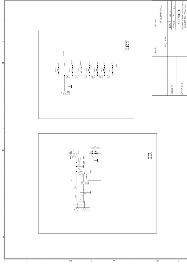
569KE01690DL
X1.0
IR, KEY
11
11
XOCECO
IR
KEY
XIAMEN OVERSEAS CHINESE
ELECTRONIC CO., LTD.
TITLE:
DWG NO.
REV.
Sheet of
DRAWN BY
APPROVED BY
GND
Vstb
+5V
Vout
C911
100n
R912
3K
C912
22u
16V
R913
47
R914510
V911
BC847AW
X911
1 2 3 4
N911
HRM538BB5117
Vout
GND
Vcc
R911
240
D911HFT503MPBR-1
R B
R9032.4K
S904
S905
R9061K
S902
S903
R9024.3K
S901
R9041.5K
S907
R90110K
X901
1 2
R9051K
S906
CH+
VOL-
VOL+
SOURCE
CH-
MENU
POWER
AB
CD
EF
1 2 3 4
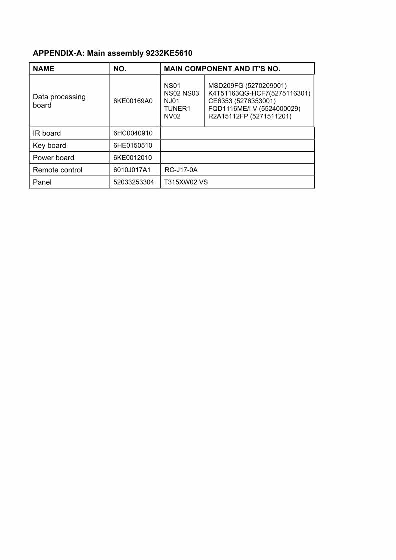
APPENDIX-A: Main assembly 9232KE5610
NAME NO. MAIN COMPONENT AND IT'S NO.
Data processing board 6KE00169A0
NS01 NS02 NS03 NJ01 TUNER1 NV02
MSD209FG (5270209001) K4T51163QG-HCF7(5275116301) CE6353 (5276353001) FQD1116ME/I V (5524000029) R2A15112FP (5271511201)
IR board 6HC0040910 Key board 6HE0150510 Power board 6KE0012010 Remote control 6010J017A1 RC-J17-0A
Panel 52033253304 T315XW02 VS
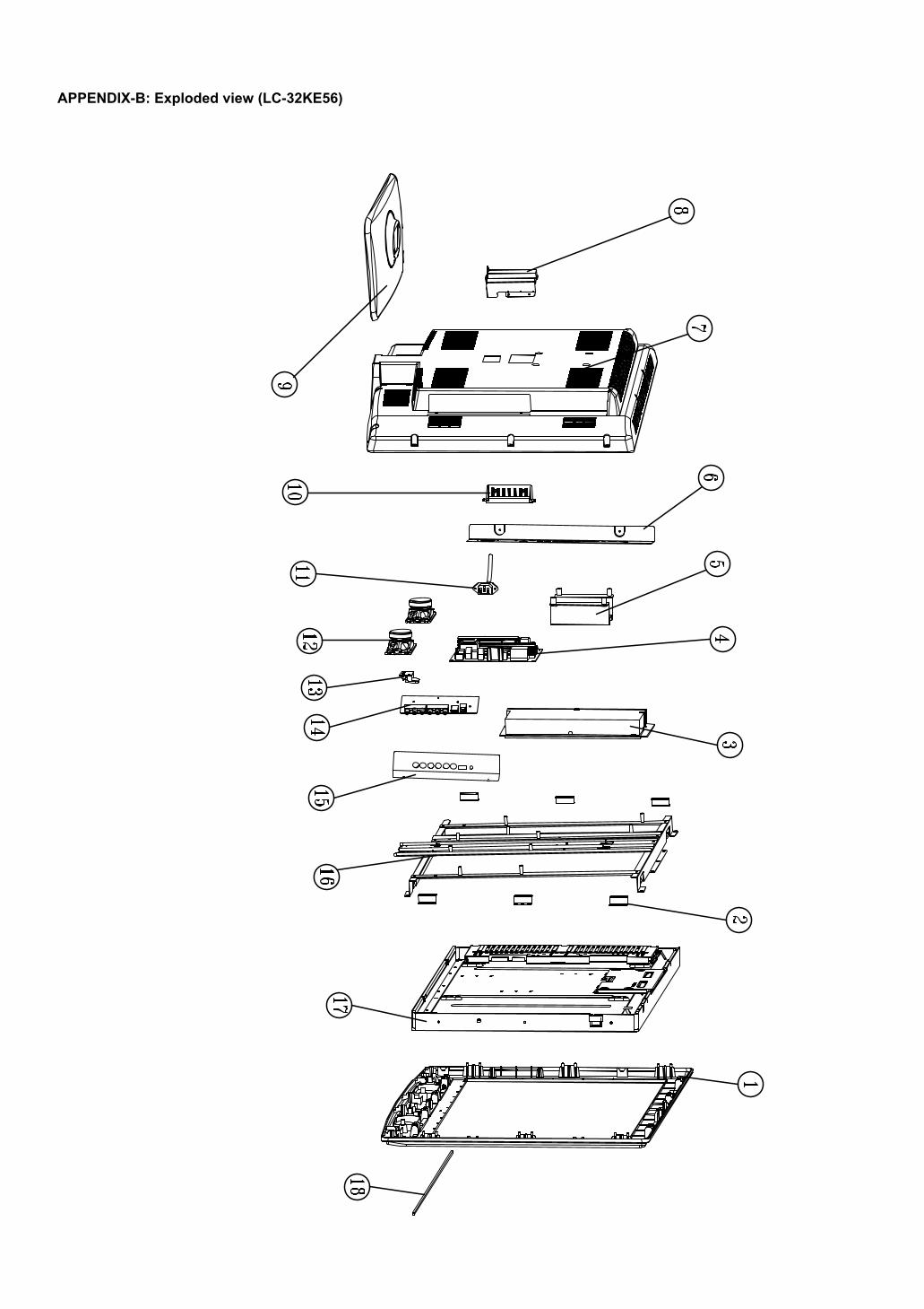
APPENDIX-B: Exploded view (LC-32KE56)
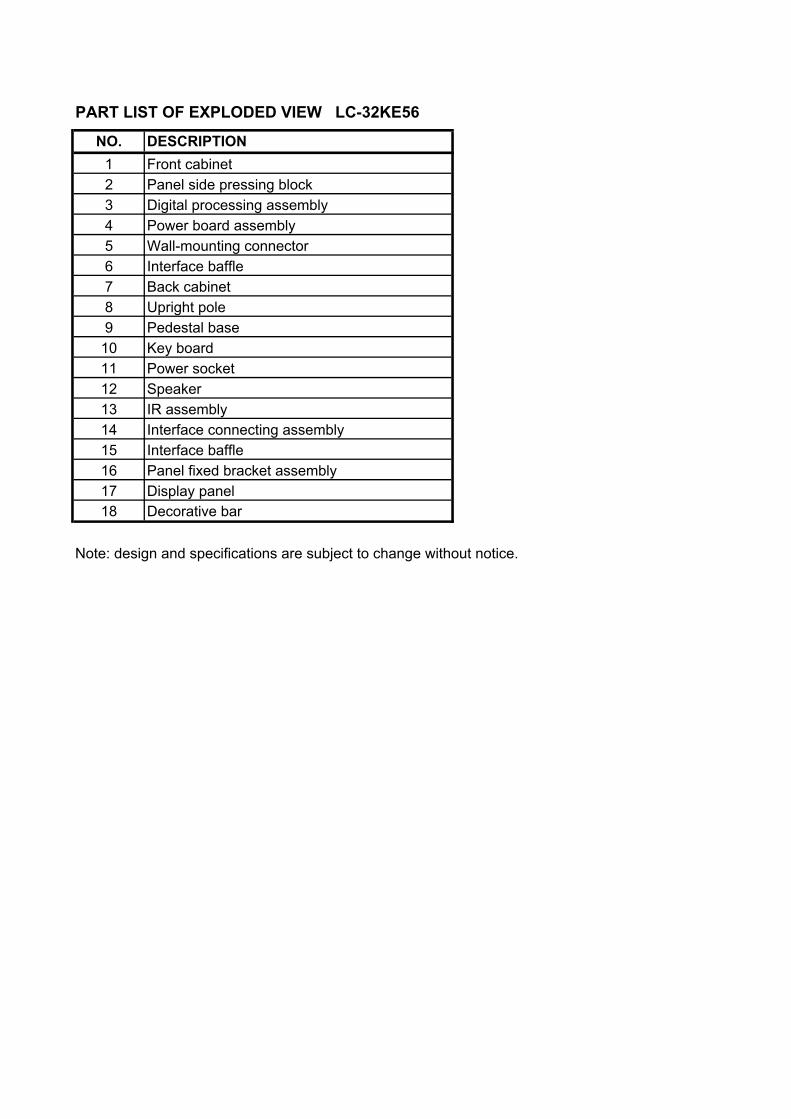
NO. DESCRIPTION1 Front cabinet2 Panel side pressing block3 Digital processing assembly4 Power board assembly5 Wall-mounting connector6 Interface baffle7 Back cabinet8 Upright pole9 Pedestal base
10 Key board11 Power socket12 Speaker13 IR assembly14 Interface connecting assembly15 Interface baffle16 Panel fixed bracket assembly17 Display panel18 Decorative bar
PART LIST OF EXPLODED VIEW LC-32KE56
Note: design and specifications are subject to change without notice.
NO. PART NO. DESCRIPTION QTY. REMARK1 5Q32560040 Front cabinet 12 581006660A Panel side pressing block 103 6KE00169A0 Digital processing assembly 14 6KE0012010 Power board assembly 15 5810063300 Wall-mounting connector 16 5810163110 Interface baffle 17 5H32561010 Back cabinet 18 58D0027400 Upright pole 19 6151154000 Pedestal base 1
10 6HE0150510 Key board 111 5282000004 Power socket 112 5500806004 Speaker 113 6HC0040910 IR assembly 114 6KE0012460 Interface connecting assembly 115 5810C66710 Interface baffle 116 6153209000 Panel fixed bracket assembly 217 5203325304 Display panel 1 T315XW02 VS18 573K245010 Decorative bar 1
·Only the parts in above list are used for repaired.·Other parts except the above parts can't be supplied.
LCD-32XR56DZ ver 1.0
PART LIST-------------------------------------------------------------------------------------------------
Components No. Panel modelback light board 19.31 XI60Z0000596 32T315XW02 VS00logic board 55.31 XI60Z0000597 32T315XW02 VS00
Note: specifications are subject to change without notice.
Assembly list of panel
66CM AND 81CM ASSEMBLE AND ATTACH THE PEDESTAL BASE
Safety Precautions
1. Please read these instructions thoroughly prior to attempting this installation. 2. Be sure to handle this product very carefully when attempting to assemble.
The manufacturer is not responsible for any damages or injuries that occur due to mishandling or improper assembly/installation.
3. When using a table or bench as an aid to assemble, be sure to put a soft cushion or covering to prevent accidental scratching or damage to the unit’s finish.
4. The speaker is not intended to support the weight of this display. Do not move or handle this product from the speaker; which can cause damage to the display not covered under the manufacturer’s warranty.
Attachment Parts : • Stand (1 piece) • M5 Screw (4 pieces) Install the Stand
1. Place the LCD TV face down on a soft cloth blanket or cushion to protect its surface from scratching. Line up the display base bracket and the base.
2. Using the supplied M5 screws (4 pieces) secure the base to the LCD TV.
3. Carefully lift the LCD off its face and stand it upright on its base.
Note
1. Appearance of this product in illustrations may differ from your actual product and is for comparative purposes only.
2. Design and specifications are subject to change without notice.

April/2009


![UQI MANUA..[1]](https://img.pdfslide.net/doc/110x75/5571feca49795991699c16b9/uqi-manua1.jpg)


![manua del[1]](https://img.pdfslide.net/doc/110x75/5571f24149795947648c651d/manua-del1.jpg)
