Embed Size (px)
Citation preview

50 • 2015 IEEE International Solid-State Circuits Conference 978-1-4799-6224-2/15/$31.00 ©2015 IEEE
ISSCC 2015 / SESSION 3 / ULTRA-HIGH-SPEED WIRELINE TRANSCEIVERS AND ENERGY-EFFICIENT LINKS / OVERVIEW
Session 3 Overview: Ultra-High-Speed Wireline Transceivers and Energy-Efficient Links
WIRELINE SUBCOMMITTEE
3.1 A 28Gb/s Multi-Standard Serial-Link Transceiver for Backplane Applications in 28nm CMOS 1:30 PMB. Zhang, Broadcom, Irvine, CA
In Paper 3.1, Broadcom presents a 28Gb/s multi-standard transceiver with data rates up to 28Gb/s in 28nm CMOS. Thereceiver has a linear equalizer and a 14-tap DFE, while the transmitter uses a source-series terminated driver with a 5-tapFFE. The transceiver compensates a 40dB loss backplane channel at 25.78Gb/s; each 0.62mm2 TX/RX consumes 295mW.
3.2 Multi-Standard 185fsrms 0.3-to-28Gb/s 40dB Backplane Signal Conditioner with Adaptive 2:00 PM Pattern-Match 36-Tap DFE and Data-Rate-Adjustment PLL in 28nm CMOST. Kawamoto, Hitachi, Tokyo, Japan
In Paper 3.2, Hitachi presents a multi-standard backplane transceiver that uses a 36-tap DFE with a pattern-capture CDRand a pattern-matching adaptive equalizer to cancel reflections due to backplane connectors. The 28nm CMOS chip operates from 0.3 to 28.05Gb/s over a 40dB loss backplane with 2 connectors.
3.3 A 0.5-to-32.75Gb/s Flexible-Reach Wireline Transceiver in 20nm CMOS 2:30 PMP. Upadhyaya, Xilinx, San Jose, CA
In Paper 3.3, Xilinx presents a fully-adaptive 0.5-to-32.75Gb/s transceiver embedded in a 20nm CMOS FPGA. The receiveruses a 15-tap DFE while the clocking circuits consist of fractional-N LC PLLs and poly-phase IQ generation circuits. Thetransceiver achieves BER <10-15 over a 10.4dB loss short-reach channel at 32.75Gb/s and a 27dB loss backplane at 28Gb/s.
Smart phones and their social apps drive tremendous growth of Internet and big data infrastructure. In turn, this spurs the insatiable need fordata communication bandwidth between chips. In this context, wireline transceivers that push the limits imposed by process technology—interms of data-rate, energy efficiency, and ability to support bursty traffic—are extremely critical. This session opens with the presentation of 3complete 28+Gb/s transceivers addressing the challenges of high channel loss (up to 40dB) and multi-standard support. Two papers then addressPAM4 signal generation/transmission for future advanced standards at higher data rates. The session concludes with a paper describing a dynamically enabled digital equalizer employed within an ADC-based link, a paper pushing the limits of rapid on/off operation in burst-mode links,and a final paper exploring calibration techniques enabling aggressive transceiver voltage scaling.
Session Chair: Ken Chang, Xilinx,San Jose, CA
Session Co-Chair: Shunichi Kaeriyama,Renesas Electronics, Tokyo, Japan

51DIGEST OF TECHNICAL PAPERS •
ISSCC 2015 / February 23, 2015 / 1:30 PM
3.4 A 36Gb/s PAM4 Transmitter Using an 8b 18GS/s DAC in 28nm CMOS 3:15 PMA. Nazemi, Broadcom, Irvine, CA
In Paper 3.4, Broadcom presents a 36Gb/s PAM4 transmitter with a clock-generation circuit. The transmitter is based onan 18GS/s 8b DAC achieving 800mVppdiff. Implemented in 28nm CMOS technology, the measured SFDR is 52 and 43dBat 0.7 and 8GHz outputs, respectively. The DAC-based transmitter consumes 84mW from 1 and 1.5V power supplies.
3.5 A 16-to-40Gb/s Quarter-Rate NRZ/PAM4 Dual-Mode Transmitter in 14nm CMOS 3:45 PMJ. Kim, Intel, Hillsboro, OR
In Paper 3.5, Intel presents a 0.0279mm2 NRZ/PAM4 transmitter (TX) operating from 16 to 40 Gb/s in 14nm tri-gateCMOS. The TX includes a feed-forward charge-injected 4:1 serializer and quarter-rate clocking and clock calibration. TheTX consumes 195 and 518mW at 28 and 40Gb/s, respectively, in NRZ mode and consumes 141 and 168mW at 33.6 and40Gb/s in PAM4 mode.
3.6 A 10Gb/s Hybrid ADC-Based Receiver with Embedded 3-Tap Analog 4:00 PMFFE and Dynamically-Enabled Digital Equalization in 65nm CMOSA. Shafik, Texas A&M University, College Station, TX
In Paper 3.6, Texas A&M University presents a 65nm 10Gb/s hybrid ADC-based receiver employing a 3-tap analog FFEembedded inside a 6b asynchronous SAR ADC, as well as a per-symbol dynamically-enabled digital equalizer. Applyingthe latter technique to the digital 4-tap FFE and 3-tap DFE results in ~30mW savings on a 36.4dB loss channel.
3.7 A 7Gb/s Rapid On/Off Embedded-Clock Serial-Link Transceiver with 20ns Power-On Time, 4:15 PM740μW Off-State Power for Energy-Proportional Links in 65nm CMOST. Anand, University of Illinois, Urbana, IL
In Paper 3.7, the University of Illinois at Urbana-Champaign presents a 7Gb/s embedded clock burst-mode transceiver toachieve energy proportional operation. Using a fast-locking LC PLL the design achieves effective throughput scaling overa 100× range (7Gb/s to 70Mb/s) while scaling the power by 44× (63.7mW to 1.43mW).
3.8 A 0.45-to-0.7V 1-to-6Gb/s 0.29-to-0.58pJ/b Source-Synchronous 4:45 PMTransceiver Using Automatic Phase Calibration in 65nm CMOSW-S. Choi, University of Illinois, Urbana, IL
In Paper 3.8, the University of Illinois at Urbana-Champaign presents a source-synchronous transceiver with aggressive supply voltage scaling to achieve energy efficiency ranging from 0.29 to 0.58pJ/b at data rates of 1 to 6Gb/s, as the supplyvoltage varies from 0.45 to 0.7V. Phase-spacing errors resulting from device mismatches are corrected using self-calibration.
3
52 • 2015 IEEE International Solid-State Circuits Conference
ISSCC 2015 / SESSION 3 / ULTRA-HIGH-SPEED WIRELINE TRANSCEIVERS AND ENERGY-EFFICIENT LINKS / 3.1
3.1 A 28Gb/s Multi-Standard Serial-Link Transceiver for Backplane Applications in 28nm CMOS
Bo Zhang, Karapet Khanoyan, Hamid Hatamkhani, Haitao Tong, Kangmin Hu, Siavash Fallahi, Kambiz Vakilian, Anthony Brewster
Broadcom, Irvine, CA
Rapid internet traffic growth has fueled the demand for bandwidth in metro networks and data centers and pushed the serial link data rate into 25Gb/s territory, populated by such electrical interface as OIF CEI-25G, CEI-28G [1],IEEE 802.3bj 100G-KR4. To cope with severe channel impairments at 25Gb/swith up to 30dB loss at Nyquist, a feed-forward equalizer (FFE)/decision feedback equalizer (DFE) based transceiver without power-hungry analog-to-digital converter (ADC) provides robust performance. This work presents a low-power and area-efficient transceiver that employs a 14-tap adaptive DFE atthe receiver (RX) and a 5-tap FFE at the transmitter (TX) for multi-standard applications up to 28Gb/s in 28nm CMOS.
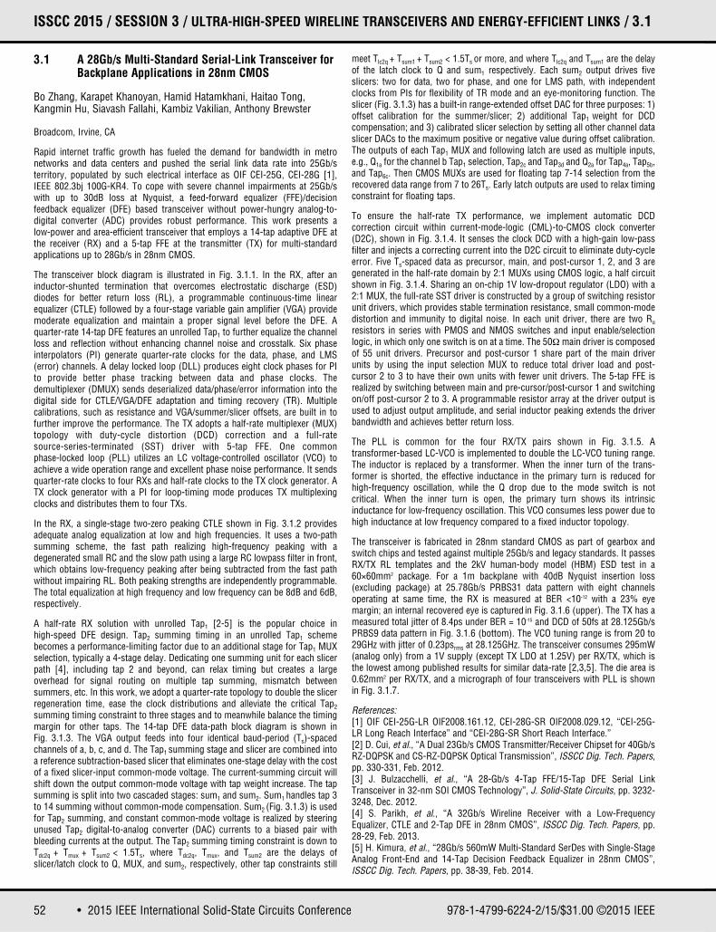
The transceiver block diagram is illustrated in Fig. 3.1.1. In the RX, after aninductor-shunted termination that overcomes electrostatic discharge (ESD)diodes for better return loss (RL), a programmable continuous-time linear equalizer (CTLE) followed by a four-stage variable gain amplifier (VGA) providemoderate equalization and maintain a proper signal level before the DFE. A quarter-rate 14-tap DFE features an unrolled Tap1 to further equalize the channelloss and reflection without enhancing channel noise and crosstalk. Six phaseinterpolators (PI) generate quarter-rate clocks for the data, phase, and LMS(error) channels. A delay locked loop (DLL) produces eight clock phases for PIto provide better phase tracking between data and phase clocks. The demultiplexer (DMUX) sends deserialized data/phase/error information into thedigital side for CTLE/VGA/DFE adaptation and timing recovery (TR). Multiple calibrations, such as resistance and VGA/summer/slicer offsets, are built in tofurther improve the performance. The TX adopts a half-rate multiplexer (MUX)topology with duty-cycle distortion (DCD) correction and a full-rate source-series-terminated (SST) driver with 5-tap FFE. One common phase-locked loop (PLL) utilizes an LC voltage-controlled oscillator (VCO) toachieve a wide operation range and excellent phase noise performance. It sendsquarter-rate clocks to four RXs and half-rate clocks to the TX clock generator. ATX clock generator with a PI for loop-timing mode produces TX multiplexingclocks and distributes them to four TXs.
In the RX, a single-stage two-zero peaking CTLE shown in Fig. 3.1.2 providesadequate analog equalization at low and high frequencies. It uses a two-pathsumming scheme, the fast path realizing high-frequency peaking with a degenerated small RC and the slow path using a large RC lowpass filter in front,which obtains low-frequency peaking after being subtracted from the fast pathwithout impairing RL. Both peaking strengths are independently programmable.The total equalization at high frequency and low frequency can be 8dB and 6dB,respectively.
A half-rate RX solution with unrolled Tap1 [2-5] is the popular choice in high-speed DFE design. Tap2 summing timing in an unrolled Tap1 schemebecomes a performance-limiting factor due to an additional stage for Tap1 MUXselection, typically a 4-stage delay. Dedicating one summing unit for each slicerpath [4], including tap 2 and beyond, can relax timing but creates a large overhead for signal routing on multiple tap summing, mismatch between summers, etc. In this work, we adopt a quarter-rate topology to double the slicerregeneration time, ease the clock distributions and alleviate the critical Tap2
summing timing constraint to three stages and to meanwhile balance the timingmargin for other taps. The 14-tap DFE data-path block diagram is shown inFig. 3.1.3. The VGA output feeds into four identical baud-period (Ts)-spacedchannels of a, b, c, and d. The Tap1 summing stage and slicer are combined intoa reference subtraction-based slicer that eliminates one-stage delay with the costof a fixed slicer-input common-mode voltage. The current-summing circuit willshift down the output common-mode voltage with tap weight increase. The tapsumming is split into two cascaded stages: sum1 and sum2. Sum1 handles tap 3to 14 summing without common-mode compensation. Sum2 (Fig. 3.1.3) is usedfor Tap2 summing, and constant common-mode voltage is realized by steeringunused Tap2 digital-to-analog converter (DAC) currents to a biased pair withbleeding currents at the output. The Tap2 summing timing constraint is down toTdc2q + Tmux + Tsum2 < 1.5Ts, where Tdc2q, Tmux, and Tsum2 are the delays ofslicer/latch clock to Q, MUX, and sum2, respectively, other tap constraints still
meet Tlc2q + Tsum1 + Tsum2 < 1.5Ts or more, and where Tlc2q and Tsum1 are the delayof the latch clock to Q and sum1 respectively. Each sum2 output drives fiveslicers: two for data, two for phase, and one for LMS path, with independentclocks from PIs for flexibility of TR mode and an eye-monitoring function. Theslicer (Fig. 3.1.3) has a built-in range-extended offset DAC for three purposes: 1)offset calibration for the summer/slicer; 2) additional Tap1 weight for DCD compensation; and 3) calibrated slicer selection by setting all other channel dataslicer DACs to the maximum positive or negative value during offset calibration.The outputs of each Tap1 MUX and following latch are used as multiple inputs,e.g., Q1a for the channel b Tap1 selection, Tap2c and Tap3d and Q2a for Tap4a, Tap5b,and Tap6c. Then CMOS MUXs are used for floating tap 7-14 selection from therecovered data range from 7 to 26Ts. Early latch outputs are used to relax timingconstraint for floating taps.
To ensure the half-rate TX performance, we implement automatic DCD correction circuit within current-mode-logic (CML)-to-CMOS clock converter(D2C), shown in Fig. 3.1.4. It senses the clock DCD with a high-gain low-passfilter and injects a correcting current into the D2C circuit to eliminate duty-cycleerror. Five Ts-spaced data as precursor, main, and post-cursor 1, 2, and 3 aregenerated in the half-rate domain by 2:1 MUXs using CMOS logic, a half circuitshown in Fig. 3.1.4. Sharing an on-chip 1V low-dropout regulator (LDO) with a2:1 MUX, the full-rate SST driver is constructed by a group of switching resistorunit drivers, which provides stable termination resistance, small common-modedistortion and immunity to digital noise. In each unit driver, there are two Ru
resistors in series with PMOS and NMOS switches and input enable/selectionlogic, in which only one switch is on at a time. The 50Ω main driver is composedof 55 unit drivers. Precursor and post-cursor 1 share part of the main driverunits by using the input selection MUX to reduce total driver load and post-cursor 2 to 3 to have their own units with fewer unit drivers. The 5-tap FFE isrealized by switching between main and pre-cursor/post-cursor 1 and switchingon/off post-cursor 2 to 3. A programmable resistor array at the driver output isused to adjust output amplitude, and serial inductor peaking extends the driverbandwidth and achieves better return loss.
The PLL is common for the four RX/TX pairs shown in Fig. 3.1.5. A transformer-based LC-VCO is implemented to double the LC-VCO tuning range.The inductor is replaced by a transformer. When the inner turn of the trans-former is shorted, the effective inductance in the primary turn is reduced forhigh-frequency oscillation, while the Q drop due to the mode switch is not critical. When the inner turn is open, the primary turn shows its intrinsic inductance for low-frequency oscillation. This VCO consumes less power due tohigh inductance at low frequency compared to a fixed inductor topology.
The transceiver is fabricated in 28nm standard CMOS as part of gearbox andswitch chips and tested against multiple 25Gb/s and legacy standards. It passesRX/TX RL templates and the 2kV human-body model (HBM) ESD test in a60×60mm2 package. For a 1m backplane with 40dB Nyquist insertion loss(excluding package) at 25.78Gb/s PRBS31 data pattern with eight channelsoperating at same time, the RX is measured at BER <10-12 with a 23% eye margin; an internal recovered eye is captured in Fig. 3.1.6 (upper). The TX has ameasured total jitter of 8.4ps under BER = 10-15 and DCD of 50fs at 28.125Gb/sPRBS9 data pattern in Fig. 3.1.6 (bottom). The VCO tuning range is from 20 to29GHz with jitter of 0.23psrms at 28.125GHz. The transceiver consumes 295mW(analog only) from a 1V supply (except TX LDO at 1.25V) per RX/TX, which isthe lowest among published results for similar data-rate [2,3,5]. The die area is0.62mm2 per RX/TX, and a micrograph of four transceivers with PLL is shownin Fig. 3.1.7.
References:[1] OIF CEI-25G-LR OIF2008.161.12, CEI-28G-SR OIF2008.029.12, “CEI-25G-LR Long Reach Interface” and “CEI-28G-SR Short Reach Interface.”[2] D. Cui, et al., “A Dual 23Gb/s CMOS Transmitter/Receiver Chipset for 40Gb/sRZ-DQPSK and CS-RZ-DQPSK Optical Transmission”, ISSCC Dig. Tech. Papers,pp. 330-331, Feb. 2012.[3] J. Bulzacchelli, et al., “A 28-Gb/s 4-Tap FFE/15-Tap DFE Serial LinkTransceiver in 32-nm SOI CMOS Technology”, J. Solid-State Circuits, pp. 3232-3248, Dec. 2012.[4] S. Parikh, et al., “A 32Gb/s Wireline Receiver with a Low-FrequencyEqualizer, CTLE and 2-Tap DFE in 28nm CMOS”, ISSCC Dig. Tech. Papers, pp.28-29, Feb. 2013.[5] H. Kimura, et al., “28Gb/s 560mW Multi-Standard SerDes with Single-StageAnalog Front-End and 14-Tap Decision Feedback Equalizer in 28nm CMOS”,ISSCC Dig. Tech. Papers, pp. 38-39, Feb. 2014.
978-1-4799-6224-2/15/$31.00 ©2015 IEEE
53DIGEST OF TECHNICAL PAPERS •
ISSCC 2015 / February 23, 2015 / 1:30 PM
Figure 3.1.1: Block diagram of the transceiver. Figure 3.1.2: Programmable two-zero continuous-time linear equalizer.
Figure 3.1.3: Block diagram of 14-tap DFE data path and schematics of summer 2 and reference-based slicer with offset calibration DAC.
Figure 3.1.5: PLL block diagram with transformer-based LC-VCO.Figure 3.1.6: 40dB backplane insertion loss and RX internal eye at 25.78Gb/s(upper) and 28.125Gb/s TX eye diagram (bottom).
Figure 3.1.4: 5-tap FFE SST driver implementation with 2:1 MUX.
3

• 2015 IEEE International Solid-State Circuits Conference 978-1-4799-6224-2/15/$31.00 ©2015 IEEE
ISSCC 2015 PAPER CONTINUATIONS
Figure 3.1.7: Die micrograph of four transceivers with a common PLL.

54 • 2015 IEEE International Solid-State Circuits Conference
ISSCC 2015 / SESSION 3 / ULTRA-HIGH-SPEED WIRELINE TRANSCEIVERS AND ENERGY-EFFICIENT LINKS / 3.2
3.2 Multi-Standard 185fsrms 0.3-to-28Gb/s 40dB Backplane Signal Conditioner with Adaptive Pattern-Match 36-Tap DFE and Data-Rate-Adjustment PLL in 28nm CMOS
Takashi Kawamoto1, Takayasu Norimatsu1, Kenji Kogo1, Fumio Yuki1, Norio Nakajima2, Masatoshi Tsuge2, Tatsunori Usugi2, Tomofumi Hokari2, Hideki Koba2, Takemasa Komori2, Junya Nasu2, Tsuneo Kawamata2, Yuichi Ito2, Seiichi Umai2, Jun Kumazawa2, Hiroaki Kurahashi2, Takashi Muto2, Takeo Yamashita2, Masatoshi Hasegawa2, Keiichi Higeta2
1Hitachi, Tokyo, Japan, 2Hitachi, Kanagawa, Japan
As processing and network speeds are accelerated to support data-rich services,the bandwidth of backplane interconnects needs to be increased while maintaining the channel length and multi-rate links. However, channel lossesand impedance discontinuities increase at high data-rates, making it difficult tocompensate the channel. In this work, we target serial links from auto-negotiation in 100G-KR4 of 0.3Gb/s to 32GFC of 28.05Gb/s in 40dB backplanearchitecture [1-3]. To achieve this challenge, there are two key techniques. First,we introduce a 36-tap decision-feedback equalizer (DFE) to cancel reflectionsdue to connectors because these reflections close the eye. To operate the 36-tapDFE, we need to fix a CDR lock-point and calculate 36-tap coefficients accurately.Thus, we develop a pattern-captured CDR with a 4b pattern filter to fix the lock-point, and a 3b pattern-matched adaptive equalizer (AEQ) to optimize 36 tapcoefficients. These techniques enable our chip to compensate 40dB channelloss. Second, we target 100G-KR4/40G-KR4/10G-KR/25G-KR and32GFC/16GFC/8GFC/4GFC. To operate across a wide range of data-rates, from0.3 to 28.05Gb/s, with low jitter, we develop a PLL architecture with two LC-VCOs and one ring VCO with a data-rate-adjustment technique by controllingan LDO. Our test chip is fabricated in 28nm CMOS. Our signal conditioner is thedemonstration to achieve the BER <10-12 PRBS31 at 100G-KR4 in a 40dB chip-to-chip backplane with two connectors by using the 36-tap DFE to cancelthe reflection and to operate across a wide range of data-rates from 0.3 to28.05Gb/s.
Figure 3.2.1 shows a backplane architecture and characteristics of a measuredchannel that consists of backplane, packages, sockets, and daughter boards. A40dB total loss and length of reflection due to connector is same as those of target backplane architecture. There are many reflections due to impedance mismatch of a DC block capacitor, packages, vias, and connectors as shown ina time-domain reflectometer (TDR). These reflections can be cancelled only byusing a DFE. In order to cancel large reflections due to the backplane connector,we introduce a 36-tap DFE.
Figure 3.2.2 shows the top-level overview. To reduce output jitter, both RX andTX have a half-rate PLL. The RXPLL generates I/Q 4-phase clock. The TXPLLtakes the role of a jitter filter to cut off the jitter in the recovered clock. In thedata-path, a continuous-time linear equalizer (CTLE) and 36-tap DFE, whose tapcoefficients are determined by the AEQ, compensate a channel loss. The recovered clock is divided by 64 to use as the reference clock of the TXPLL. An8:1 multiplexer (MUX) generates pre/main/post1/post2 4-phase data for a 4-tapfeed-forward equalizer (FFE). A rate-detect circuit recognizes the data rate andthen configures the blocks for a given data-rate if the rate is changed. For low-speed links <4.0Gb/s such as the auto-negotiation in the 100G-KR4, thebypass path is selected. This architecture supports a wide data-rate range from0.3 to 28.05Gb/s.
Figure 3.2.3 shows a block diagram of the 36-tap DFE, pattern-matched AEQ,and pattern-captured CDR. The data feeds even/odd 3-to-36 tap current-summerDFE and tap-1 and tap-2 loop-unrolled DFE [2]. The 36-tap DFE has designissues related to the delay of the current-summer DFE and optimization of tapcoefficients. First, if the delay of the current-summer DFE is large, the ISI cannot
be cancelled sufficiently. To reduce this delay, the summed current of tap coefficients 3 to 36 (H3 to H36) are added to the data. Second, if the tap coefficients are not accurate, the ISI and reflections cannot be cancelled sufficiently. To optimize the tap coefficients, it is necessary to fix the CDR lock-point and balance tap coefficients between data patterns. For a long tracechannel, a data edge is affected by the data pattern due to residual ISI. The transitions in the Nyquist patterns of 01 and 10 may not cross over the thresholdvoltage (+/-W) due to a lack of equalization. Thus, the CDR cannot use these patterns for phase detection. If the CDR does detect all data edges, the CDR lock-point varies, causing insufficient DFE equalization due to large variation ofthe tap coefficients [4]. To avoid this problem and reduce the variation of thelock-point, the CDR should select captured data patterns. Moreover, the CDRcaptures the data before the tap coefficients are added to the data. Thus, if dataof tap-1 and tap-2 is 01 and 10, the CDR may fail to capture the data or the CDRlock-point variation is large due to the residual ISI. Thus, the CDR should capturethe data when the data of taps 1 and 2 is 00 and 11. To solve these issues, wedevelop a pattern-captured CDR by using a pattern filter. The CDR captures 0001pattern to fix the lock-point. The pattern-captured CDR with 4b pattern filterreduces the variation of the lock-point from 10 to 1.7ps and the residual ISI from20 to 9ps for a 40dB channel.
Figure 3.2.4 shows the developed RXPLL architecture that incorporates twoLCVCOs and one ring VCO (RVCO) with a data-rate-adjustment technique usingLDOs. The RVCO oscillates from 2 to 11GHz, covering from 4 to 22Gb/s. The LC-VCO25G oscillates from 22 to 26GHz and 4-phase half-rate clocks are generated by a divide-by-2. The LC-VCO25G covers from 22 to 26Gb/s in half-rate mode and from 11 to 13Gb/s in full-rate mode. The LC-VCO28G coversfrom 26 to 29Gb/s and from 13 to 14.5Gb/s. To solve the trade-off between4GHz frequency range and 0.2psrms jitter, we develop a data-rate-adjustmenttechnique by controlling the LDO. The LC-VCO oscillation frequency can be controlled by the LDO output voltage. As the LDO output voltage is lowered, theamplitude of oscillation signals reduce, increasing the frequency of oscillation.The LC-VCO achieves the 4GHz frequency range with 4b coarse tuning and LDOcontrol technique from 0.45 to 0.65V. The LC-VCO frequency range is increasedfrom 1.8 to 4.5GHz by the data-rate-adjustment technique. There are severalcombinations between LDO output voltage and LC-VCO bands in which the PLLcan lock. After the LC-VCO and LDO are calibrated, the lowest LDO output voltage is selected to save power.
Figure 3.2.5 shows measured results of a 40dB backplane between trace BERT-to-chip at 100G-KR4 PRBS31. The BER is <10-12 at TX output signal whenthe equalization budget is 18dB CTLE, 12dB FFE, and 10dB DFE. When the number of the DFE taps is less than 36, the BER is not <10-12 because the largereflections due to the connectors are not cancelled. The tap-1 coefficientbecomes large to equalize the ISI. The tap-31 and tap-32 coefficients are largeto cancel the reflection due to the far-side connector. We achieve <185fsrms
random jitter from 7MHz to 10GHz.
Figure 3.2.6 shows measurement results of the 40dB chip-to-chip backplanetrace at 100G-KR4 PRBS31. The BER is <10-12. Our signal conditioner canachieve 40dB loss compensation at 25.78125Gb/s and cover data rates from 0.3to 28.05Gb/s. The chip area is 5.5×4.6mm2 shown in Fig. 3.2.7.
References:[1] U. Singh, et al, “A 780mW 4x28Gb/s Transceiver for 100GbE Geabox PHY in40nm CMOS,” ISSCC Dig. Tech. Papers, pp. 40-41, Feb. 2014. [2] J.F. Bulzacchelli, et al., “A 28Gb/s 4-Tap FFE/15-Tap DFE Serial LinkTransceiver in 32nm SOI CMOS Technology,” ISSCC Dig. Tech. Papers, pp. 324-325, Feb. 2012.[3] H. Kimura, et al., “28Gb/s 560mW Multi-Standard SerDes with Single-StageAnalog Front-End and 14-Tap Decision Feedback Equalizer in 28nm CMOS.”ISSCC Dig. Tech. Papers, pp. 38-39, Feb. 2014.[4] V. Balan, et al., “A 130mW 20Gb/s Half-Duplex Serial Link in 28nm CMOS,”ISSCC Dig. Tech. Papers, pp. 438-439, Feb. 2014.
978-1-4799-6224-2/15/$31.00 ©2015 IEEE

55DIGEST OF TECHNICAL PAPERS •
ISSCC 2015 / February 23, 2015 / 2:00 PM
Figure 3.2.1: Target backplane architecture and channel characteristics. Figure 3.2.2: Top-level overview of backplane signal conditioner.
Figure 3.2.3: 36-tap DFE, pattern-matched AEQ, CDR overview.
Figure 3.2.5: Measured BER and tap-coefficients in BERT-to-chip 40dB backplane trace. Figure 3.2.6: Measured BER and performance summary.
Figure 3.2.4: RXPLL overview and schematic of LDO and LC-VCO.
3

• 2015 IEEE International Solid-State Circuits Conference 978-1-4799-6224-2/15/$31.00 ©2015 IEEE
ISSCC 2015 PAPER CONTINUATIONS
Figure 3.2.7: Chip micrograph.

56 • 2015 IEEE International Solid-State Circuits Conference
ISSCC 2015 / SESSION 3 / ULTRA-HIGH-SPEED WIRELINE TRANSCEIVERS AND ENERGY-EFFICIENT LINKS / 3.3
3.3 A 0.5-to-32.75Gb/s Flexible-Reach Wireline Transceiver in 20nm CMOS
Parag Upadhyaya, Jafar Savoj, Fu-Tai An, Ade Bekele, Anup Jose, Bruce Xu, Daniel Wu, Didem Turker, Hesam Aslanzadeh, Hiva Hedayati, Jay Im, Siok-Wei Lim, Stanley Chen, Toan Pham, Yohan Frans, Ken Chang
Xilinx, San Jose, CA
The introduction of high-speed backplane transceivers inside FPGAs hasaddressed critical issues such as the ease in scalability of performance, highavailability, flexible architectures, the use of standards, and rapid time to market.These have been crucial to address the ever-increasing demand for bandwidth incommunication and storage systems [1-3], requiring novel techniques in receiver (RX) and clocking circuits.
Figure 3.3.1 shows the transceiver architecture with reconfigurable clock generation consisting of two fractional-N LC PLLs per quad and a ring PLL perchannel. Since the receiver and the transmitter (TX) require half-rate clock frequencies, the LC PLLs must cover a frequency range of 8 to 16.375GHz fordata-rates of 16 to 32.75Gb/s. Lower data-rates are covered by dividing the frequency of the LC PLLs. Each PLL has two LC oscillators to provide a wide tuning range (>45% each) and these two PLLs have an overlap to allow two independent frequencies around 10G standards (covering 9.5 to 13.1GHz). ThePLL consists of synchronized CMOS down-counter frequency divider and a programmable sigma-delta (ΣΔ) modulator. The fractional PLL can be configured in either a MASH 1-1 (2nd order) or MASH 1-1-1 (3rd order) architecture by programming the (ΣΔ) modulator. The frequency resolution isalso programmable from 12 to 24 bits in steps of 4 bits.
Each LC PLL is followed by a passive wide-range 2nd order polyphase filter (PPF)[4] for quadrature generation for high data-rates (>16.375Gb/s). For lower data-rates, a frequency divider divides the LC PLL frequency by two and produces quadrature signals. A multiplexer selects the PPF or the divider outputdepending on the speed of operation. The PPF circuit uses a two-stage constant-phase topology whose pole locations are chosen to track the frequencyrange of the preceding PLL. Poles are selected such that over PVT variationsmagnitude differences are within the tolerable range. A low-distortion linearbuffer ensures low harmonic distortion to minimize I/Q error.
The differential high-speed I and Q clock signals are routed to the four transceiver channels. A long chain of CML buffers achieve good supply-noiseimmunity but suffer DC-offset accumulation and I/Q mismatch errors. A capacitive-degenerated CML buffer is inserted in every three buffer stages toattenuate DC gain as shown in Fig. 3.3.1. An additional duty-cycle correction(DCC) and I/Q calibration scheme is implemented in each transceiver channel toensure good phase-interpolator (PI) linearity, which impacts receiver jitter tolerance margin [5].
Figure 3.3.2 shows the top-level block diagram of the clock DCC and I/Q correction scheme that can be used for both foreground and background calibrations. The duty-cycle distortion (DCD) is corrected for both I and Q phasesprior to I/Q correction. The DCC and I/Q correction share the analog front-endwith an auto-zeroed pre-amplifier to cancel out the offsets. The DCC correctionscheme utilizes capacitor degeneration and 7b current DAC along with digitalcalibration logic. The correction range covers ±5ps of DCD, which is equivalentto 16% correction range at 16GHz clock with <150fs residual error. The correction part of I/Q error calibration uses a CML-based variable delay witherror correction range of ±5ps. An offset-calibrated symmetrical XOR is used tosense I/Q error to achieve <180fs resolution.
Figure 3.3.3 shows the receiver, which consists of a 3-stage inductively peakedCTLE and a summer, and a 15-tap 1b unrolled DFE. To meet the high bandwidthrequirement of the receiver over process corners and to minimize bandwidthvariation, the load resistors of the CTLE and summer stages are calibratedagainst an external resistor. The summer circuit is the 4th stage in a cascade oflinear amplifier stages, necessitating stringent linearity requirements. To achievehigh linearity, high current density for the summer input transistors is desired,resulting in reduced the headroom for the tail transistors over the PVT corners.To help ease this tradeoff between linearity and tail source headroom, source
degeneration is added to the summer. The source degeneration resistance isimplemented as a small array of NMOS transistors and is digitally programmable. The summer circuit utilizes a common-mode feedback bias(CMFB) circuit to stabilize its output common mode to a level suitable for theproceeding slicers. The CMFB loop detects the output common mode at the output of the summer through large resistors and controls the top PMOS gate.
A capacitively loaded summer (which sees 7 slicers and 15 differential pairstaps) requires high bandwidth on two paths; a forward path from CTLE to summer output, and a feedback path from DFE taps to summer output. Shuntpeaking is used over a T-coil solution because in shunt peaking both forward andfeedback paths see the same load and achieve very similar bandwidths whereasfor a T-coil solution effective bandwidths are different between these two paths.Shunt peaking bandwidth extension ratio is usually a maximum of around 1.72×,which is enough to meet the bandwidth requirements of the summer.
The DFE circuit has 15 taps with the first bit unrolled. Note that in a generic DFEtopology, the data (D) samples and the crossing (X) samples appear such that Xlags D by 0.5 unit interval (UI), i.e., it uses late crossing. This configuration produces satisfactory results at higher data-rates. However, at lower data-rates,DFE tap feedback path can be completed in less than 0.5UI and there is notenough hold time for X samples. In order to resolve this issue, the DFE circuit isprogrammed such that for high data-rates X samples lag D samples by 0.5UI(i.e., D even (0°), X even (90°), D odd (180°), X odd (270°)) and for low data-rates, X samples lead D samples by 0.5UI (i.e., D even (0°), X odd (90°), Dodd (180°), X even (270°)), as shown in Figure 3.3.4. The early/late crossingswap allows optimal link performance for all data-rates.
The transceiver is fabricated in a 20nm CMOS process and assembled in a flip-chip package. Figure 3.3.5(a) shows the receiver internal stressed eye scanat 32.75Gb/s over 10.4dB loss very short-reach (VSR) channel, and (b) at28Gb/s 27dB loss long-reach (LR) channel. These measurements exclude package losses and account for crosstalk of 12 adjacent running lanes. Figure3.3.5(c) shows the receiver jitter tolerance at 32.75Gb/s. The output transmit eyediagram at 32.75Gb/s utilizing PLL in integer N mode is shown in Fig. 3.3.5(d).Figure 3.3.6 summarizes the transceiver performance. Figure 3.3.7 depicts thedie micrograph.
Acknowledgments:The authors thank the entire Xilinx SERDES design team as well as Sai LalithChaitanya Ambatipudi, Santiago Asuncion, Ryan Bruno, Jayesh Patil andVaibhav Kamdar for their valuable lab support.
References:[1] H. Kimura, et al., “28Gb/s 560mW Multi-Standard SerDes with Single-StageAnalog Front-End and 14-Tap Decision-Feedback Equalizer in 28nm CMOS,”ISSCC Dig. Tech. Papers, pp. 38-39, Feb. 2014.[2] U. Singh, et al., “ A 780mW 4×28Gb/s Transceiver for 100GbE Gearbox PHYin 40nm CMOS,” ISSCC Dig. of Tech. Papers, pp. 40-41, Feb. 2014.[3] J. Bulzacchelli, et al., “A 28-Gb/s 4-Tap FFE/15-Tap DFE Serial LinkTransceiver in 32-nm SOI CMOS Technology,” ISSCC Dig. Tech. Papers,pp. 324-325, Feb., 2012.[4] F. Behbahani, et al., “CMOS mixers and polyphase filters for large imagerejection,” IEEE J. Solid-State Circuits, vol. 36, no. 6, pp. 873 –887, June 2001.[5] G.R. Gangasani et al., “A 16-Gb/s Backplane Transceiver with 12-Tap CurrentIntegrating DFE and Dynamic Adaptation of Voltage Offset and Timing Drifts in45-nm SOI CMOS Technology,” Proc. CICC, Sept. 2011.
978-1-4799-6224-2/15/$31.00 ©2015 IEEE

57DIGEST OF TECHNICAL PAPERS •
ISSCC 2015 / February 23, 2015 / 2:30 PM
Figure 3.3.1: Transceiver architecture with two fractional-N LC PLLs. Figure Figure 3.3.2: Duty cycle and IQ error correction circuit.
Figure 3.3.3: Receiver front-end for 15-tap, 1-bit speculative DFE topology.
Figure 3.3.5: Receiver eye scan for (a) 32.75 Gb/s VSR and (b) 28Gb/s LRchannels; (c) RX jitter tolerance and (d) transmit eye at 32.75 Gb/s. Figure 3.3.6: Performance summary.
Figure 3.3.4: Early/Late (D/X Swap) crossing swap architecture.
3

• 2015 IEEE International Solid-State Circuits Conference 978-1-4799-6224-2/15/$31.00 ©2015 IEEE
ISSCC 2015 PAPER CONTINUATIONS
Figure 3.3.7: Die micrograph (2.700×2.213mm2).

58 • 2015 IEEE International Solid-State Circuits Conference
ISSCC 2015 / SESSION 3 / ULTRA-HIGH-SPEED WIRELINE TRANSCEIVERS AND ENERGY-EFFICIENT LINKS / 3.4
3.4 A 36Gb/s PAM4 Transmitter Using an 8b 18GS/s DAC in 28nm CMOS
Ali Nazemi, Kangmin Hu, Burak Catli, Delong Cui, Ullas Singh, Tim He, Zhi Huang, Bo Zhang, Afshin Momtaz, Jun Cao
Broadcom, Irvine, CA
At data rates beyond 10Gb/s, most wireline links employ NRZ signaling. SerialNRZ links as high as 56Gb/s and 60Gb/s have been reported [1]. Nevertheless,as the rate increases, the constraints imposed by the channel, package, and diebecome more severe and do not benefit from process scaling in the same fashion that circuit design does. Reflections from impedance discontinuities inthe PCB and package caused by vias and connectors introduce significant signalloss and distortions at higher frequencies. Even with an ideal channel, at everypackage-die interface, there is an intrinsic parasitic capacitance due to the padsand the ESD circuit amounting to at least 150fF, and a 50Ω resistor terminationat both the transmit and receive ends resulting in an intrinsic pole at 23GHz orlower. In light of all these limitations, serial NRZ signaling beyond 60Gb/sappears suboptimal in terms of both power and performance. Utilizing variousmodulation techniques such as PAM4, one can achieve a higher spectral efficiency [2]. To enable such transmission formats, high-speed moderate-resolution data converters are required. This paper describes a 36Gb/s transmitter based on an 18GS/s 8b DAC implemented in 28nm CMOS, compliantto the new IEEE802.3bj standard for 100G Ethernet over backplane and coppercables [3].
The transmitter is composed of 20:1 multiplexers using a 1V power supply andthe output DAC-driver utilizing a 1.5V supply (Fig. 3.4.1). The DAC is combinedwith the output driver [5] and is based on the current-steering topology. AnNMOS segmented current DAC with shunt-peaked load is used to achieve thebandwidth required. In such a topology, the main trade-off is between the number of DAC coarse bits encoded through thermometer-weighted currentcells and the number of fine bits encoded through binary-weighted currentcells [4]. The higher number of coarse bits increases the number of current cells,which improves linearity but also introduces more parasitic capacitance at theDAC output and lowers the bandwidth. Furthermore it increases complexity andpower consumption since each current cell requires its own multiplexer androuting to the output pads, regardless of its size. In this work, we segment theDAC into 2b thermometer-encoded and 6b binary-encoded current cells, resulting in a total of 9 current cells including 3 thermometer-weighted currentcells and 6 binary-weighted current cells (Fig. 3.4.2). This reduces both parasiticcapacitance and power consumption. However, the main drawback of increasingthe number of bits that are binary-encoded is the higher requirement on the current cell matching at the border between binary-weighted current cells andthermometer-weighted current cells. The matching requirement to meet the DNLconstraint and ensure monotonicity at bit n is described by the following equation:
Ik is the current of the kth bit. For each increase in the order of the highest bit thatis binary-encoded, the matching requirement as a percentage of the current In
rises by a factor of 2, increasing the size of the unit current cell by a factor of 4.This could result in significantly higher parasitic capacitance in the currentsource and a higher overall DAC area. To minimize the current cell size and realize the 2b thermometer 6b binary segmentation scheme, a coarse bit calibration circuit is implemented and will be described later.
As shown in [4], the linearity of the DAC depends on the output impedance ofthe current source. The third harmonic in full swing conditions can be approximated by HD3 = (RLN/4|Zout|)2 where |Zout| is the output impedance of theLSB current source, RL the resistor load of the DAC, and N the total number oflevels (in this DAC N = 256). At lower frequencies, Zout is essentially resistive andbeyond several GHz it becomes mostly capacitive due to the capacitance seen atthe source node of the DAC switches (Fig. 3.4.2). The use of a cascode deviceMc increases the output impedance at both low and high frequency and isolatesthe drain of the current source with significantly higher capacitance Ccs, from thesource of the DAC switch. Nevertheless, at very high frequencies, the cascodedevice is less effective and some of the capacitance Ccs appears at the output ofthe DAC through the cascode parasitic capacitances Cgd, Cgs and Cds of Mc.Hence, it is important to ensure that Ccs is minimized by reducing the size of thecurrent source as much as possible, yet ensuring the matching requirement forINL and DNL. The same calibration circuit helps achieve this goal.
Figure 3.4.3 describes the DAC coarse bit calibration circuit. The calibration isperformed only for the 2 MSB bits that are encoded as thermometer-weightedcurrent sources. This corresponds to 3 unit current cells I6, which are 64× thesize of the LSB current cell. At start-up, the sum of all the current cells for lowerbits for ∑0Ik + ILSB is compared to a reference current Iref. Iref is trimmed until itsvalue is equal to ∑0Ik + ILSB. In the next step, each I6 current cell is connected tothe calibration node and trimmed against Iref. The coarse bit calibration circuitallows one to reduce the size of the unit current cell by 2×, reducing Ccs whilemeeting the DNL and monotonicity requirement for the 8b DAC.
The 20:1 multiplexer is entirely based on CMOS gates and serializes twenty900Mb/s data streams into 18Gb/s. The highest clock frequency provided to theMUX is 9GHz hence the last stage of multiplexing is performed at half-rate,reducing the power consumption. The input of the DAC needs a common modeof around 1V to allow enough headroom for the current cells. Therefore, 18Gb/slevel shifters using exclusively thin-oxide devices and resistive loads aredesigned to change the digital logic levels from 0 to 1V to 0.6 to 1.5V (Fig. 3.4.3).In this circuit, the device M1 protects M0 from over-voltage stress and the cross-coupled PMOS pair M2 improves DCD of the 18Gb/s signals. The optimalswing to ensure that the current switches entirely in the DAC cell (IResidue < ILSB)and the switch transistor oxides are not over-stressed, is around 900mV. Ananalog servo-loop (Fig. 3.4.3) compares the logic level at the output of a replicacircuit and ensures that the single-ended swing is maintained around the optimalvalue over PVT.
The phase of the 9GHz reference clock for the transmitter is controlled by aphase interpolator circuit with a resolution of 434fs (256 steps). Since the transmitter DAC has a finite settling time, some of the clock phase noise is converted into SNR, and hence needs to be minimized. The VCO phase noise issuppressed at the output by increasing the PLL bandwidth to around 8MHz. Thenoise contribution of all other PLL blocks becomes more significant at suchbandwidths and needs to be reduced. A differential change pump with large biascurrent is used to reduce its output noise contribution. The loop filter uses alarge integrator capacitance to reduce the zero resistor and its noise [6].
The transmitter is implemented in 28nm CMOS and occupies a total active areaof 0.05mm2. The DAC performance is characterized using a high-bandwidthspectrum analyzer. The SFDR exceeds 47dB up to 2GHz and 38dB up to theNyquist frequency of 9GHz (Fig. 3.4.4). The THD exceeds 6b up to 3GHz and5.5b up to the Nyquist frequency. The DAC bandwidth is measured and the lossis <2dB at 9GHz. The measured transmitter output random jitter is 109fsrms. Thedual mode transmitter can generate NRZ (18Gb/s) and PAM-4 (36Gb/s) formatdata streams achieving over 800mVppdiff of full scale amplitude (Fig. 3.4.5). TheISI in the NRZ mode is below 3ps and the rise/fall time is lower than 11ps whilethe PAM-4 horizontal eye opening is about 0.67UI. The DAC enables equalizationthrough the DSP. The power consumption of the transmitter is 84mW and thePLL and clock distribution is 60mW. A comparison table for the DAC has beenprovided in Fig. 3.4.6 and this design achieves the best FOM while occupying thesmallest area among the compared designs. A chip micrograph is provided inFig. 3.4.7. This 18GS/s 8b DAC enables more complex modulation and signalprocessing in future wireline applications.
Acknowledgment:The authors thank Justin Nguyen and Darren Chee for their support.
References:[1] Y.M. Greshishchev, et al., “A 56GS/s 6b DAC in 65nm CMOS with 256x6bmemory,” ISSCC Dig. Tech. Papers, pp. 194-196, Feb. 2011.[2] A. Amirkhany, et al., “A 24Gb/s Software Programmable Analog Multi-toneTransmitter,” IEEE J. Solid-State Circuits, vol. 43, no. 4, pp. 999-1009, Apr.2008.[3] IEEE Standard 802.3bj-2011 “Physical Layer Specifications and ManagementParameters for 100 Gb/s Operation over Backplanes and Copper Cables”.[4] C-H. Lin, et al., “A 12b 2.9GS/s DAC with IM3<-60dBc beyond 1GHz in 65nmCMOS,” ISSCC Dig. Tech. Papers, pp. 74-75, Feb. 2009.[5] J. Savoj, et al., “A 12-GS/s phase calibrated CMOS Digital-to-AnalogConverter for Backplane Communications,” IEEE J. Solid-State Circuits, vol. 43,no. 5, pp. 1207-1216, May 2008. [6] B. Raghavan, et al., “A sub-2W 39.8-to-44.6Gb/s transmitter and receiverchipset with SFI-5.2 interface in 40nm CMOS,” ISSCC Dig. Tech. Papers, pp. 32-33, Feb. 2013.
978-1-4799-6224-2/15/$31.00 ©2015 IEEE
5
5

59DIGEST OF TECHNICAL PAPERS •
ISSCC 2015 / February 23, 2015 / 3:15 PM
Figure 3.4.1: Block diagram of the transmitter and the clock generation PLL. Figure 3.4.2: Diagram of the 8b DAC.
Figure 3.4.3: (a) Block diagram of the calibration circuit (b) Diagram of the18Gb/s level shifter circuit and amplitude control servo-loop.
Figure 3.4.5: Dual mode operation: eye diagram for 18Gb/s (left) NRZ and36Gb/s (right) PAM-4 without equalization.
Figure 3.4.6: Comparison table with published (>10GS/s) digital-to-analogconverters.
Figure 3.4.4: (a) Measured SFDR and THD vs. frequency (b) Normalizedamplitude of the DAC vs. frequency (normalized to 800mVppdiff).
3

• 2015 IEEE International Solid-State Circuits Conference 978-1-4799-6224-2/15/$31.00 ©2015 IEEE
ISSCC 2015 PAPER CONTINUATIONS
Figure 3.4.7: Die micrograph.
60 • 2015 IEEE International Solid-State Circuits Conference
ISSCC 2015 / SESSION 3 / ULTRA-HIGH-SPEED WIRELINE TRANSCEIVERS AND ENERGY-EFFICIENT LINKS / 3.5
3.5 A 16-to-40Gb/s Quarter-Rate NRZ/PAM4 Dual-Mode Transmitter in 14nm CMOS
Jihwan Kim, Ajay Balankutty, Amr Elshazly, Yan-Yu Huang, Hang Song,Kai Yu, Frank O’Mahony
Intel, Hillsboro, OR
Emerging standards in wireline communication are defining a path to data-ratesof 40Gb/s and beyond. Most previous standards for these networking applications use NRZ signaling. However, practical signal integrity constraintshave led to a renewed interest in also supporting PAM4 for some applicationsand loss profiles [1-2]. Recently, several transmitters have been reported thatoperate between 28 and 60Gb/s using NRZ or PAM4 modulation exclusively [2-4]. However, high-speed SerDes building blocks that support both a wide frequency range and multiple forms of modulation provide more compatibilitybetween components and avoid the development of multiple IPs. In addition,these blocks must continue to scale into the next-generation of CMOS processtechnologies to lower the cost by reducing area and power consumption. Thispaper presents a dual-mode transmitter (TX) implemented in 14nm CMOS thatsupports both NRZ and PAM4 modulations and operates from 16 to 40Gb/s. TheTX incorporates a 4-tap NRZ FIR filter that is reconfigurable to drive PAM4 levels, quarter-rate clocking with a high-bandwidth 4:1 serializer, a duty-cycleand quadrature-error correction circuit with statistical phase error detection, andcompact, multi-layer T-coils for pad capacitance (Cpad) reduction.
The TX block diagram is presented in Fig. 3.5.1. An on-chip pattern generatorsends 8b parallel data to a mode selector through a 16:8 MUX. The data is further serialized for 4-tap FFE in NRZ mode or split into four 2b bundles (MSBand LSB) in PAM4 mode, and fed into the output stage that consists of 36 segments to cover equalization/modulation as well as PVT variation of the termination resistance. Each segment contains a retimer, an equalization (EQ)selector, a single-ended-to-differential (S2D) converter, a 4:1 serializer, a pre-driver, and a source-series terminated (SST) driver with a shared resistor.Figure 3.5.1 also illustrates the output stage segmentation for both NRZ andPAM4 modes. In NRZ mode, the segments are divided into three parts: cursor/1st
pre-cursor, cursor/2nd pre-cursor, and cursor/post-cursor which contain ¼, ¼,and ½ of the total number of segments, respectively. The configurability of theNRZ TX taps supports a wide range of channel profiles while minimizing thenumber of segments. In PAM4 mode, the MSB is fed to ⅔ of the segments andthe LSB is fed to ⅓ of the segments to generate four different voltage levels without providing equalization. The TX maintains quarter-rate clocking and operates at half the symbol rate of NRZ mode to maintain the same data andclock paths.
While half-rate and quarter-rate architectures ideally consume the same CV2fpower, a quarter-rate serialization scheme can be an attractive solution at veryhigh data-rates because it relaxes the speed and timing requirements in the serializer. Figure 3.5.2 (a) shows the 4:1 serializer using back-to-back pass-gates. Compared to a 2:1 serializer, the 4:1 serializer relaxes the criticaltiming path by 2UI that is set by tck-q+td+tsetup<3UI, where tck-q, td, and tsetup are ck-to-q delay of the retimer, data buffer delay, and the setup time of the serializer, respectively. However, this topology suffers from poor ISI at the output because of charge-sharing effect at the intermediate node between twopass-gates. The junction and interconnect parasitic capacitance adds non-negligible ISI because large pass-gates are used to minimize the series resistance. When one of the four branches is transmitting data (e.g., CK4_90 andCK4_180 are high and d1 is transmitted), one of the pass-gates in adjacentbranch is inevitably turned on as well (by CK4_90), enabling a path to anotherparasitic capacitance (at node X), which increases ISI at the output. To resolvethis issue, a feed-forward charge-injection technique is used as shown inFig. 3.5.2 (b). Auxiliary branches with smaller pass-gates forward the same datato the internal node of previous bit’s branch to charge up and reduce the outputISI. Simulations at 40Gb/s show ISI is reduced by 77% and eye height isincreased by 30% at the worst-case condition, adding only 10% to the serializerclock buffer power.
The TX driver is a voltage-mode SST type with a shared resistor. This architecture is primarily chosen to minimize the effective Cpad at the driver outputand reduce power consumption compared to a CML driver. Within the enabledsegments, the effective Cpad associated with the switch transistor diffusion androuting parasitics to the resistor is significantly reduced due to the resistive
division between the switch and the resister (1:5 in this design). The sharedresistors along with driver junction parasitic diodes provide the secondary ESDprotection and effectively reduce the required size of ESD diodes. Furthermore,sharing the resistor reduces overall Cpad by halving the amount of the resistorused for termination and avoids un-driven internal terminals compared with anunshared resistor SST driver [4]. Even with these optimizations, further reduction of the total Cpad is still required to achieve the adequate bandwidth for40Gb/s operation, and a compact multi-layer on-chip T-coil is used. The T-coil,shown in Fig. 3.5.3, splits the total inductance asymmetrically to absorb the different values of the driver and ESD diodes parasitic capacitance. It is implemented using two adjacent metal layers to maximize the inductance perunit area. The measured T-coil inductance is 750pH, self-resonant frequency(SRF) is 38GHz, and size is 35×45μm2. The T-coil ESR of about 5Ω at DC is usedas part of the driver output resistance. In simulation, the T-coil reduces the effective Cpad by over 60% across all frequencies and extends the 3dB bandwidthby a 2.3× (from 10 to 23GHz).
The quarter-rate TX requires I/Q clocks with minimal duty-cycle and quadratureerror. Figure 3.5.4 shows the duty-cycle/quadrature-error detection (DCD/QED)and correction (DCC/QEC) blocks. The clock distribution is implemented in full-swing CMOS to achieve better area scaling than CML. Fanouts are chosen toprovide adequate bandwidth and minimize jitter amplification. The DCD/QEDsenses I/Q clocks generated by a digital DLL [5] at the output of the clock bufferin the TX. The duty-cycle error is measured by comparing the accumulated number of ones when sampling the P/N clocks with the asynchronous VCO(fosc ≈ 4GHz) [6]. The quadrature-error is then detected, in a similar way to [7],by measuring the overlap between I/Q clocks. An FSM controls the DCC that iscomposed of programmable delay cells with rising/falling edges being independently adjusted by pull-up/pull-down controls and the QEC that containsvariable capacitive loads for I/Q error correction.
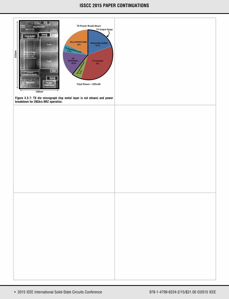
Two TX lanes are fabricated in a 14nm tri-gate CMOS process (Fig. 3.5.7). EachTX (excluding PLL and LDO) occupies 130×215μm2. A quarter-rate clock from apair of LC-PLLs drives the TX, and measured eye diagrams with PRBS7 including the effect of 12 to 14dB channel loss are shown in Fig. 3.5.5. The TXachieves RJ of 300/380fsrms for 14/20GHz clock patterns at the output. At28/40Gb/s, TJ is 10.7/12.9pspp and ISI is 4.13/4.46pspp in NRZ mode. In PAM4mode, a software-based CTLE is applied at the scope (Adc=0.5, z1=2.5GHz,p1=4.5GHz, p2=16GHz for 33.6Gb/s and 20GHz for 40Gb/s, and gain peaking ofless than 4dB) to emulate the effect of a practical RX CTLE and equalize for thechannel loss. The PAM4 eye widths and heights are 0.87/0.65UI and 102/61mV,respectively, at 33.6/40Gb/s. The TX consumes 195/518mW at 28/40Gb/s inNRZ mode and 141/168mW at 33.6/40Gb/s in PAM4 mode. The power consumption at 40Gb/s in NRZ mode is significantly higher than designedbecause the TX is fabricated in a low-power logic version of the process technology that requires an elevated supply voltage only for NRZ mode at40Gb/s. Nonetheless, the data indicates a clear power benefit for PAM4 operation from 28 to 40Gb/s. The performance of the TX is summarized inFig. 3.5.6, and the power breakdown for NRZ operation at 28Gb/s is shown inFig. 3.5.7.
Acknowledgements:The authors thank W. Y. Li, H. S. Kim, K. Chandrashekar, A. Mezhiba, D. Shi, K.Nguyen, D. John, R. Singhal, B. D. Grossnickle, J. Bondie, D. Baker, K.Rasmussen, C. Walker, and Z. Qian for valuable contributions to this work.
References:[1] Optical Interconnect Forum (OIF) [Online]. Available:http://www.oiforum.com/public/currentprojects.html [2] P.-H. Chiang, et al., “60Gb/s NRZ and PAM4 Transmitters for 400GbE in65nm CMOS,” ISSCC Dig. Tech. Papers, pp. 42-43, Feb. 2014.[3] A. A. Hafez, et al., “A 32-to-48Gb/s Serializing Transmitter Using MultiphaseSampling in 65nm CMOS,” ISSCC Dig. Tech. Papers, pp. 38-39, Feb. 2013.[4] C. Menolfi, et al., “A 28Gb/s Source-Series Terminated TX in 32nm CMOSSOI,” ISSCC Dig. Tech. Papers, pp. 334-335, Feb. 2012. [5] A. Elshazly, et al., “A 2GHz-to-7.5GHz Quadrature Clock-Generator UsingDigital Delay Locked Loops for Multi-Standard I/Os in 14nm CMOS,” IEEE Symp.VLSI Circuits, pp. 52-53, June 2014.[6] T. -C. Hsueh, et al., “A 25.6Gb/s Differential and DDR4/GDDR5 Dual-ModeTransmitter with Digital Clock Calibration in 22nm CMOS,” ISSCC Dig. Tech.Papers, pp. 444-445, Feb. 2014.[7] M. Mansuri, el al., “An On-Die All-Digital Delay Measurement Circuit with250fs Accuracy,” IEEE Symp. VLSI Circuits, pp. 98-99, June 2012.
978-1-4799-6224-2/15/$31.00 ©2015 IEEE

61DIGEST OF TECHNICAL PAPERS •
ISSCC 2015 / February 23, 2015 /3:45 PM
Figure 3.5.1: Block diagram of the dual-mode TX, channel loss profile, andsegmentation for NRZ/PAM4 modes.
Figure 3.5.2: (a) 4:1 serializer using back-to-back pass-gates, and (b) proposed feed-forward charge injected 4:1 serializer.
Figure 3.5.3: The multi-layer T-coil and simulated reflection/bandwidth of TXdriver.
Figure 3.5.5: Measured TX eyes including test channel (PAM4 eyes includesoftware-based CTLE at scope). Figure 3.5.6: TX performance comparison.
Figure 3.5.4: Block diagram of the duty-cycle/quadrature-error detection/correction circuits.
3
• 2015 IEEE International Solid-State Circuits Conference 978-1-4799-6224-2/15/$31.00 ©2015 IEEE
ISSCC 2015 PAPER CONTINUATIONS
Figure 3.5.7: TX die micrograph (top metal layer is not shown) and powerbreakdown for 28Gb/s NRZ operation.

62 • 2015 IEEE International Solid-State Circuits Conference
ISSCC 2015 / SESSION 3 / ULTRA-HIGH-SPEED WIRELINE TRANSCEIVERS AND ENERGY-EFFICIENT LINKS / 3.6
3.6 A 10Gb/s Hybrid ADC-Based Receiver with Embedded 3-Tap Analog FFE and Dynamically-Enabled Digital Equalization in 65nm CMOS
Ayman Shafik, Ehsan Zhian Tabasy, Shengchang Cai, Keytaek Lee, Sebastian Hoyos, Samuel Palermo
Texas A&M University, College Station, TX
ADC-based receivers are currently being proposed in high-speed serial linkapplications to enable flexible, complex, and robust digital equalization in orderto support operation over high loss channels [1-3]. However, the power dissipation of the ADC, as well as the digital equalization that follows, is a majorconcern for wireline receiver applications [3]. In this work, a hybrid ADC-basedreceiver architecture is presented that introduces innovations in both the ADCand the digital equalizer design. First, an analog 3-tap feed-forward equalizer(FFE) is efficiently embedded into a 6b time-interleaved SAR ADC, allowing forreductions in both ADC resolution and digital equalizer complexity. Second, significant power reduction is achieved by detecting reliable symbols at the ADCoutput and dynamically enabling/disabling the digital equalizer.
Figure 3.6.1 shows PAM2 BER bathtub curves for two backplane channels withdifferent attenuations. The low-loss channel has an open eye with a voltageregion over which a two-level slicer can reliably detect both ‘0’ and ‘1’ symbolsat the required BER. Increased ISI from the high-loss channel causes thereceived eye to close with a slicer threshold set at the nominally optimal zerolevel, where significant errors are observed. In this case, typical receiversemploy equalization on all received symbols to reduce ISI and open the eye toachieve the target BER. Certain received signal levels, however, have a very lowprobability of generating an error for a given symbol and do not necessarilyrequire additional equalization. Our hybrid ADC-based receiver takes advantageof this to save power by employing a three-level detector with programmablethresholds that allows for reliable detection of both ‘0’ and ‘1’ symbols when thereceived signal falls outside the ambiguous region, and dynamically disables thedigital equalizer on a per-symbol basis. For symbols in the ambiguous regionthat cannot be reliably detected, the digital equalizer is dynamically enabled tofurther remove ISI and achieve the target BER. Combining this technique withembedded FFE in the ADC allows for a significant reduction in digital equalizerpower. The embedded FFE reduces the percentage of symbols in the ambiguousregion [4].
The hybrid ADC-based receiver utilizes a 32-way time-interleaved 6b SAR ADCwith embedded 3-tap FFE, as shown in Fig. 3.6.2. This 10GS/s converter haseight parallel sub-ADCs, each consisting of a front-end T/H clocked at 1.25GHzfollowed by four asynchronous unit SAR ADCs. A differential divide-by-four circuit is used with 5GHz complementary input clocks to generate the eightphases spaced at 100ps that clock the sub-ADC T/Hs. Digitally controlled capacitor banks, with a <0.4ps resolution and ~30ps range, are employed to calibrate timing mismatches in the clock distribution to the T/H blocks. The ADCincludes calibration DACs for comparator offset, linear gain, and sampling clockskew. A switched-capacitor implementation allows for efficient embedding of the3-tap FFE, which includes one pre-cursor and one post-cursor taps, into thecapacitive DAC (CDAC) of the unit SAR ADCs [5]. In each unit ADC, the T/Hn
input is sampled onto capacitor CS to realize the main cursor with unity gain,while the post-cursor tap coefficient α1 for the previous sample (T/Hn-1) and thepre-cursor tap coefficient α-1 for the next sample (T/Hn+1) are set with the CDACweighting during the sampling phase.
Following the front-end ADC is a dynamically enabled digital equalizer, consisting of a 4-tap FFE and 3-tap DFE, which further equalizes any unreliablesymbols. As shown in Fig. 3.6.3, latches are inserted in the equalizer computation path to only enable switching of the adders and multipliers if thedigital threshold detector decides that an unreliable symbol is received.Additional multiplexers controlled by the threshold detector are placed after theloop-unrolled DFE digital slicers to select either the un-equalized reliable symbolfrom the ADC output or the further digitally equalized bits. While the additionaldigital threshold detector, latches, and multiplexers add a 19% power overheadrelative to an always active equalizer, when combined with an ADC with embedded FFE the power savings are significant due to the relatively low activityfactor of the equalizer computation path. In order to accommodate various channels, reconfiguration of the 4-tap FFE is possible with a main-cursor select
control that allows all combinations ranging from all pre-cursor to all post-cursor equalization taps. A loop-unrolled architecture is utilized to meet the critical feedback timing paths of the digital 3-tap DFE [6], with a pipeline registerbank inserted to improve the timing slack before the DFE selection multiplexers.The digital equalizer is fully synthesized using a digital standard-cell library andauto-placed-and-routed. To enable 10Gb/s operation, we use a 32-way time-interleaved parallel implementation where each slice is clocked at312.5MHz.
Figure 3.6.7 shows a die micrograph of the hybrid ADC-based receiver, fabricated in a GP 65nm CMOS process. The core time-interleaved ADC and digital equalizer occupy 0.38mm2 and 0.39mm2, respectively, with other circuitry, such as the T/Hs, clock phase generation, reference buffers, and interface re-timing blocks bringing the total area to 0.81mm2. 10Gb/s PRBS datais passed through various FR4 channels from a Centellax PCB12500 transmitmodule and the receiver digital equalizer output is fed back to the BERT for performance characterization. Here no transmit equalization is used, with theembedded FFE in the ADC and the dynamically enabled digital equalizer makingup all the equalization in the system. Figure 3.6.4 shows timing margin bathtubcurves for four FR4 channels with attenuations ranging from 20.9 to 36.4dB atthe 5GHz Nyquist frequency, when an additional 1.5dB loss from the receiverboard and package is included. First considered is the performance with onlyembedded ADC equalization activated, with both the embedded pre- and post-cursor FFE taps having a range of 33LSB and a resolution of 1.1LSB (Fig. 3.6.5).For this case, open eyes with timing margins exceeding 0.3UI are observed forthe two lowest-loss channels. However, the two highest-loss channels requirecollaborative use of both the embedded and digital equalizers to obtain an openeye. When the digital equalizer is dynamically enabled on a per-symbol basis,timing margins of 0.2UI and 0.1UI are obtained for the 31.7 and 36.4dB channels, respectively, at a BER<10-10. Figure 3.6.5 shows how digital equalizerpower is saved with the hybrid-ADC receiver architecture for seven FR4 channelswith attenuation ranging from 12.1 to 36.4dB. For channels with up to 25dBattenuation, the embedded equalizer alone opens the eye, translating into thedigital equalizer being disabled 100% of the time and ideally all the digital equalizer power saved. When the power overhead due to the enable latches andthreshold detector switching and leakage currents is considered, this slightlydegrades to more than 80% power savings. For higher attenuation channelswhen the digital equalizer is enabled, the hybrid architecture achieves digitalequalizer power savings of around 75% for up to 36.4dB channel attenuation.The ADC, T/Hs, and clock phase generation dissipate 79mW of power and thedigital equalizer consumes 38mW, out of which more than 30mW can be savedby the dynamic-enabling of the hybrid architecture. Figure 3.6.6 compares thiswork with other ADC-based receivers operating near 10Gb/s [1-3]. The presented receiver is able to support operation over the highest loss channelamong these designs, while also providing significant power savings in the digital equalizer.
Acknowledgment: This work was supported in part by the Semiconductor Research Corporationunder Task 1836.111 through the Texas Analog Center of Excellence (TxACE)and the National Science Foundation under Grant EECS-1202508. The authorsalso thank R. Payne from Texas Instruments for helpful discussions.
References:[1] M. Harwood, et al., “A 12.5Gb/s SerDes in 65nm CMOS using a baud-rateADC with digital receiver equalization and clock recovery,” ISSCC Dig. Tech.Papers, pp. 436-591, Feb. 2007.[2] E.-H. Chen, et al., “Power optimized ADC-based serial link receiver,” IEEE J.Solid-State Circuits, vol. 47, no. 4, pp. 938-951, Apr. 2012.[3] B. Zhang, et al., “A 195mW / 55mW dual-path receiver AFE for multistandard8.5-to-11.5 Gb/s serial links in 40nm CMOS,” ISSCC Dig. Tech. Papers, pp. 34-35, Feb. 2013.[4] A. Shafik, et al., “Embedded equalization for ADC-based serial I/O receivers,”IEEE Electr. Perform. Electron. Packaging Syst., pp. 139–142, Oct. 2011.[5] E. Zhian Tabasy, et al., “A 6b 10GS/s TI-SAR ADC with embedded 2-tapFFE/1-tap DFE in 65nm CMOS,” IEEE Symp. VLSI Circuits Dig. Tech. Papers, pp.274-275, June 2013.[6] S. Kasturia and J.H. Winters, “Techniques for high-speed implementation ofnonlinear cancellation,” IEEE J. Select. Areas Commun., vol. 9, no. 5, pp. 711-717, June 1991.
978-1-4799-6224-2/15/$31.00 ©2015 IEEE

63DIGEST OF TECHNICAL PAPERS •
ISSCC 2015 / February 23, 2015 / 4:00 PM
Figure 3.6.1: Receiver voltage margin BER bathtub curves with low- and high-loss channels, and block diagram of the hybrid ADC-based receiver.
Figure 3.6.2: 32-way time-interleaved asynchronous SAR ADC with embedded3-tap FFE.
Figure 3.6.3: Dynamically enabled digital equalizer with 4-tap reconfigurableFFE and 3-tap loop-unrolled DFE.
Figure 3.6.5: Hybrid ADC-based receiver digital equalizer power savings vs.channel attenuation (BER <10-10), embedded 3-tap FFE range and resolution,and power breakdown. Figure 3.6.6: Performance summary and comparison table.
Figure 3.6.4: Receiver BER bathtub curves for 4 FR4 channels.
3

• 2015 IEEE International Solid-State Circuits Conference 978-1-4799-6224-2/15/$31.00 ©2015 IEEE
ISSCC 2015 PAPER CONTINUATIONS
Figure 3.6.7: Die micrograph of the hybrid ADC-based receiver.

64 • 2015 IEEE International Solid-State Circuits Conference
ISSCC 2015 / SESSION 3 / ULTRA-HIGH-SPEED WIRELINE TRANSCEIVERS AND ENERGY-EFFICIENT LINKS / 3.7
3.7 A 7Gb/s Rapid On/Off Embedded-Clock Serial-Link Transceiver with 20ns Power-On Time, 740μWOff-State Power for Energy-Proportional Links in 65nm CMOS
Tejasvi Anand1, Mrunmay Talegaonkar1, Ahmed Elkholy1, Saurabh Saxena1, Amr Elshazly2, Pavan Kumar Hanumolu1
1University of Illinois, Urbana, IL, 2Intel, Hillsboro, OR
Energy-proportional operation of serial links is imperative for realizing energy-efficient data centers and low-power mobile interfaces such as MIPI [1].Burst-mode communication, where the link is powered-off when idle and powered-on when needed, achieves energy proportional operation [2]. Ideally, aburst mode link must be turned on/off in zero time, must consume zero powerin the off-state and must incur zero energy overhead while making on/off transitions. However, these requirements are difficult to meet in practice and asa consequence, the efficacy of burst mode communication in achieving energyproportional operation is reduced. The main challenges in achieving smallpower-on time and off-state power include the design of fast-locking PLLs,CDRs and achieving fast settling of bias node voltages. In this paper, we presenta complete 7Gb/s energy-proportional embedded-clock transceiver that achievesless than 20ns power-on time while consuming 63.7mW on-state power,0.74mW off-state power and 1.2nJ of total transition energy penalty per burst.
Figure 3.7.1 shows the block diagram of the transceiver. The transmitter is composed of parallel PRBS generators, a 16:1 mux, and a fast power-on CMLdriver with 3-tap FFE. The transmitter together with the PLL is powered-on by anexternal start signal while the receiver powers-on automatically upon detectingincoming data. Both transmitter and receiver share a low power on-chip temperature sensor and a 7GHz fast power-on LC-PLL. The PLL can be configured to operate in either transmitter or in receiver mode, and has an optionto be configured in either proportional or bang-bang control. Also shown inFig. 3.7.1 is the receiver consisting of a Start Rx generator, quarter-rate BBPD,four 1.75GHz fast power-on phase interpolators (PIs), fast power-on CDR withdynamic-gain-control logic, three 4:16 demuxes and parallel PRBS checkers.The loop gain of the digitally controlled PI based CDR loop is adaptively adjustedto minimize lock time. Instead of taking a majority vote of early and late signals,they are de-muxed and provided to the CDR logic. By adjusting the PI phasebased on the number of early and late signals, the clock phase of the data sampler is quickly aligned to the center of incoming data. The recovered data isde-muxed to the parallel PRBS checker that is also designed to operate in burst-mode. Biasing of the PI and of the CML output driver is left powered-on inthe off-state. This greatly reduces power-on time at the expense of 40μWincrease in the off-state power. Receiver lock time is estimated from Error signal,which is generated by performing logical OR operation on parallel PRBS checkeroutputs. Receiver lock is declared when the Error signal goes low.
Figure 3.7.2 shows the block diagram of fast power-on digital LC-PLL. It uses ahybrid architecture wherein the proportional and integral paths are implementedin analog and digital domain, respectively [5]. Storing the digital frequency control word in the integral path accumulator during the off-state and restoringit back at power-on ensures that PLL starts in frequency-locked condition.However, this does not guarantee rapid phase locking because of the perturbation caused by the unknown initial input phase offset (ΔΦ = ΦREF-DEL – ΦFB-DEL). Conventional PLLs rely on feedback action to force ΔΦ= 0, and as a result have long lock time that is inversely proportional to the PLLbandwidth. In this work, we seek to reduce lock time by making ΔΦ = 0 onpower-on without using the PLL feedback. The two main components that causeΔΦ ≠ 0 are: (a) unknown initial phase of the DCO and (b) delay in the feedbackpath of PLL. To mitigate the former, LC-DCO is kick-started by a pulse having aknown phase relationship with the reference clock. This makes the DCO take thesame phase trajectory during every power-on transient, which results in thedivided DCO output signal (FBDEL) to appear with a fixed phase offset (ΔΦ = ΦX)from the delayed reference signal (REFDEL). This offset is corrected by a DLLsuch that ΔΦ = 0. Because ΦX can be as large as 1 reference period (≈10ns), theDLL must have a very wide range. To ease the range requirement, a ripple-counter-based divider with programmable set/reset control is used as a
coarse delay line to set ΦX to be within one DCO period. The DLL uses PFD output and tunes the digitally controlled delay line (DCDL) such that ΦX = 0 insteady state. The fine DCDL has 250ps range and approximately 2ps resolution.This phase alignment is performed once during initial startup and is kept on during regular power-on/off operation. To bring FBDEL closer to REFDEL, the DLLmoves the DCDL by just one LSB step on each power on/off transition (see timing in Fig. 3.7.2). Note that DLL does not influence PLL loop dynamics insteady state. A replica of DCDL and divider in REFDEL path helps to maintainphase alignment even in the presence of voltage and temperature variations during long power-off periods. A 64×8 look up table (LUT) and associated logicfor tracking LC frequency with temperature is also incorporated at the expenseof one reference cycle power-on latency.
Figure 3.7.3 shows the measured PLL and transmitter results. Absolute phasedrift of PLL output (captured using Agilent DSO-81204A, 1ns after the power-ontransient) in both proportional and bang-bang control modes indicates thatimplemented phase calibration reduces the PLL lock time to <1ns and the phasedrift to ±3ps. The capture span is approximately 2 to 3 time constants of the PLLloop and beyond this span PLL feedback ensures that the phase does not driftbeyond ±3ps. With 100mV of DLL supply variation during power-off state, errorin the phase drift is less than 2ps. At 7GHz output frequency, the PLL achievesan integrated jitter of 435fsrms and reference spur of -50.1dBc while consuming4.8mW on-state power and 41.6μW off-state power. The measured power-ontime of CML output driver is less than 500ps.
Figure 3.7.4 shows the measured results of transceiver with PRBS7 data captured after 4 billion on-off transitions. When the transmitter is powered-on,output common-mode voltage drops from VDD to VDD – VSWING/2, where VSWING isthe transmitter output swing. Start Rx generator senses this change in commonmode and powers on the receiver. CDR achieves lock within 20ns of power-on.The latency of the parallel PRBS checker to generate Error signal to go low,which is approximately 3 to 4 CDR clock cycles (≈7ns) is included in the power-on time of 20ns. Lock time is observed to be proportional to the amount of ISIin the data, and the reported power-on time is with an eye opening of 0.25UI atthe input of the samplers (see the bathtub plot in Fig. 3.7.4). Measured JTOL corner frequency in always-on case is around 2MHz.
Energy proportional behavior of the complete transceiver in operation is verifiedand results are shown in Fig. 3.7.5. For 128-byte data bursts, the transceiverachieves 100× effective data-rate scaling (7Gb/s to 70Mb/s) while scaling thepower by 44× (63.7 to 1.43mW) and energy efficiency by only 2.2× (9.1 to20.5pJ/b). For 8-byte data burst, compared to the always-on case, the transceiver achieves 26× energy efficiency improvement at 70Mb/s. The performance of the transceiver and PLL is compared to the state-of-the-art inFig. 3.7.6. Among the cited designs, the LC PLL achieves lowest reported power-on time without compromising its energy efficiency and jitter performance. This work demonstrates energy-proportional operation in anembedded clock architecture. The die micrograph is shown in Fig. 3.7.7.
Acknowledgment:This research was supported in part by Intel Labs University Research Office,SRC under task ID: 1836.129, and NSF under CAREER EECS-0954969. We thankBerkeley Design Automation for providing Analog Fast Spice (AFS) simulator.Thanks to Seong Joong Kim and TwistedTraces for their help in testing.
References:[1] D. Abts et al, “Energy proportional datacenter networks,” in Proc. ISCA,2010, pp. 338-347.[2] B. Leibowitz et al, “A 4.3 GB/s mobile memory interface with power-efficientbandwidth scaling,” IEEE J. Solid-State Circuits, vol. 45, no. 4, pp. 889-898, Apr.2010.[3] R. Navid et al, “A 25 GHz 100 ns lock time digital LC PLL with an 8-phaseoutput clock,” in Proc. IEEE Symp. VLSI Circuits, 2013, pp. 196–197.[4] T. Anand et al, “A 2.5 GHz 2.2 mW/25μW on/off-state power 2 psrms -long-term-jitter digital clock multiplier with 3-reference-cycles power-on time,”ISSCC Dig. Tech. Papers, pp. 256–257, Feb. 2013.[5] W. Yin et al, “A 0.7-to-3.5 GHz 0.6-to-2.8 mW highly digital phase-lockedloop with bandwidth tracking,” IEEE J. Solid-State Circuits, vol. 46, no. 8,pp. 1870-1880, Aug. 2011.
978-1-4799-6224-2/15/$31.00 ©2015 IEEE

65DIGEST OF TECHNICAL PAPERS •
ISSCC 2015 / February 23, 2015 / 4:15 PM
Figure 3.7.1: Block diagram of the 7Gb/s energy proportional transceiver.Figure 3.7.2: Block diagram of the fast power-on LC-PLL and timing diagramof background phase calibration logic.
Figure 3.7.3: On/off measurements of the PLL and transmitter.
Figure 3.7.5: Measured energy efficiency and power at different data-ratesobtained by duty cycling the transceiver for three different data burst lengths.
Figure 3.7.6: Performance summary and comparison with state-of-the-artdesigns.
Figure 3.7.4: Measured on/off behavior of the transceiver along with themeasured JTOL and bathtub plot at the input of receiver samplers.
Quarter Rate BBPD
START RxGeneratorCDR Logic
5050
KPKI
DGCL
LSB4
2+5
16
16
4
4
START Rx
Error Acc.
Data
Error
16 +-
PRBS Checker16 4ErrCnt.
14Early
Late
START Tx
START PLL
REF
TemperatureSensor
PRBS 7,15,23,31Generator
Prog. Divider
16:2
D Q
D Q
D Q
D Q
D Q
D Q
50 50
2:13-Tap FFE
2
START TS
÷2
6
Receiver
Transmitter
START Tx
Acc-Acc-F
Fast Power-onLC-PLL 7GHz
START PLL
FBDEL
REFDEL
PFD Input
x
UP DN
REFDEL FBDEL
Q D
S R
Q D
S R
Q D
S R
PLLOUT
STARTLCH
STARTLCH
STARTLCH
PFD
Replica of Delay Line and Divider
Retiming
TEMP
REF
START PLL
8
Fast Power-on LC-DCO
Background Phase Calibration Logic
Fine Delay Line - DCDL(Capacitively Tuned)
8
UP
DN
Bin toTherm.
Coarse Delay Line (Divider)
BBPD
7
DLL
STARTLCH
STARTLCH
UP DN
D QDFF
Frequency in/out
LUT (64x8)
Frequency word indexed by temperature
Address
Timing & Control
REF-DEL FB-DEL
6
Transmitter Power-On Transmitter Power-Off
START Tx
500ps
Tx is On200ps
PLL Output Phase, 1ns after Power-on PLL Output Phase (Zoom-in)
16bit Parallel PRBS Checker
Rec. Data
Error16
PRBS Checker
Zoom in
CDR Locked
20nsSTART Rx
Error
Recovered Data
Recovered Clock
Captured Receiver Transient with Complete Transceiver Powered-on/off
0.25UI
Always-on JTOL Always-on Bath-tub
This Work[3] [2] [4] Dunwell
Architecture PLL PLL PLL MDLL MILOTechnology 65nm GP 40nm 40nm LP 90nm 65nmSupply [V] 1 NA 1.1 1.1 1.1Output Freq. [GHz] 7 25 4.3 2.5 2.3-4Reference [MHz] 109.375 390 537.5 312.5 790Integrated Jitter [fs] 435 394 N/A 752 N/APower-on Time [ns] 1 100 241.8 10 10Power Efficiency[mW/GHz] 0.68 2.56 NA 0.88 30.4
On Power [mW] 4.8 64 NA 2.2 96Off Power [ W] 41.6 N/A NA 25 N/A
This Work
Architecture EmbeddedClock Forwarded Clock
Technology 65nm GP 40nm LPSupply [V] 1/1.1 1.1Peak data rate [Gb/s] 7 2.7-4.3Power-on time [ns] Less than 20 241.8Efficiency [pJ/bit] 9.1 3.3On-state power [mW] 63.7 14.2Off-state power [ W] 740 50De/Serialization Ratio 16:1 8:1
Area [mm2] 1.7+
(1750μmx975μm)0.92*
(1544μmx594μm)
PLL Comparison Table
Transceiver Comparison Table
* Reported for 8 memory lanes+ Area includes de-cap, pads & test logic
3

• 2015 IEEE International Solid-State Circuits Conference 978-1-4799-6224-2/15/$31.00 ©2015 IEEE
ISSCC 2015 PAPER CONTINUATIONS
Figure 3.7.7: Die micrograph of the transceiver.
1750µm
950µ
m
PLLLUT
Tx4xPI
BBPD
3x 16:1Demux
CDRPRBSChecker
PR
BS
Gen
.

66 • 2015 IEEE International Solid-State Circuits Conference
ISSCC 2015 / SESSION 3 / ULTRA-HIGH-SPEED WIRELINE TRANSCEIVERS AND ENERGY-EFFICIENT LINKS / 3.8
3.8 A 0.45-to-0.7V 1-to-6Gb/s 0.29-to-0.58pJ/b Source-Synchronous Transceiver Using Automatic Phase Calibration in 65nm CMOS
Woo-Seok Choi1, Guanghua Shu1, Mrunmay Talegaonkar1, Yubo Liu1, Da Wei1, Luca Benini2, Pavan Kumar Hanumolu1
1University of Illinois, Urbana, IL, 2University of Bologna, Bologna, Italy
Supply voltage (VDD) scaling offers a means to greatly reduce power in serial linktransceivers. Ideally, power efficiency at a given data rate can be improved byreducing VDD while increasing the number of multiplexed circuits operating inparallel at lower clock frequencies [1]. Though increasing the amount of parallelism is desirable to scale VDD, in practice, it is limited by two main factors.First, increased sensitivity to device variations (threshold voltage/dimensionmismatch) at lower VDD makes it extremely challenging to generate equallyspaced multi-phase clocks needed in multiplexed transmitter and receiver.Phase calibration methods can correct phase-spacing errors [2,3], but theireffectiveness at lower VDD is limited as the calibration circuits themselvesbecome sensitive to device variations. Second, as oscillator output swingreduces with VDD, its phase noise degrades, making low-noise clock generationdifficult to implement with low power dissipation. Phase noise can be suppressed by embedding the oscillator in a wide bandwidth analog phase-locked loop (APLL), but conventional charge-pump-based APLLs are difficult to design at low supply voltages (VDD <0.5V). Digital PLLs (DPLLs) canoperate at low VDD, but they suffer from conflicting noise bandwidth tradeoffs,which prevent increasing the bandwidth to suppress oscillator phase noise adequately. In this paper, we present a phase-calibration method that enablesthe operation of a source-synchronous transceiver down to VDD of 0.45V. Theenergy efficiency and data-rate of the prototype transceiver scale from 0.29 to0.58pJ/b and 1.3Gb/s to 6Gb/s, respectively, as VDD is varied from 0.45 to 0.7V.
Figure 3.8.1 shows the block diagram of the source-synchronous transceiver.The data transmitter (Tx) is composed of an 8:1 output-multiplexed single-endedvoltage-mode (VM) output driver and a self-calibrated PLL-based multi-phasegenerator. Using 8 equally spaced phases provided by the PLL, the output driverserializes 8b parallel data into a 1b full-rate data stream. In each of the 8 slicesof output driver, data bit, Di, is gated with one unit interval (UI) pulse generatedby performing AND operation on two adjacent clock phases, Φi+1, and Φi
(i = 0~7). Compared to a conventional VM driver, this implementation is bettersuited for low voltage operation as it reduces the number of stacked devices inthe output driver [4]. The output swing is set to 200mVpp using an on-chip low-dropout regulator implemented using a pseudo-differential common-sourceerror amplifier architecture for low-voltage operation. NMOS transistors in theoutput driver (M1i and M2i) are sized to have output impedance close to 50Ω.Instead of a full-rate clock, a 1/8th rate clock is forwarded to the receiver using aVM driver to save power.
Also shown in Fig. 3.8.1 is the un-terminated receiver (Rx) consisting of 8 parallel offset-cancelled low-voltage slicers, clocked by 8 phases provided by thePLL. It samples the transmitted serial data and generates 8 de-serialized datastreams. Each slicer is implemented using a modified sense-amplifier in whichoffset cancellation is performed at the output using a digitally tunable capacitorarray. De-skewing needed to mitigate path mismatch between the data and clockchannels is performed using a single digitally controlled delay line (DCDL) in theforwarded clock path. A limiting amplifier converts low-swing forwarded clockinto a rail-to-rail signal and feeds it to the DCDL, whose output is used as reference clock to the PLL. Similar to Tx PLL, the Rx PLL also employs the developed phase-calibration method to compensate for phase spacing errors.
The block diagram of the low-voltage PLL is shown in Fig. 3.8.2. Using analogproportional path and digital integral path, this hybrid architecture helps extendthe PLL bandwidth thereby achieving low noise performance with low powerconsumption [5]. To minimize reference spur caused by offset and non-zero set-up time of the bang-bang phase detector used in the integral path, a symmetric NAND-based decision circuit is used for generating digital E/L outputs. The VCO is implemented using a 4-stage ring oscillator consisting ofdual control pseudo-differential delay stages. Current source IC that is commonto all the delay stages is controlled by the PLL, while the output capacitor in eachof the delay stages is separately controlled by the calibration loop. In the absenceof calibration, Monte Carlo simulations indicate that the standard deviation of thephase mismatch is around 12% at VDD = 0.5V, reducing to 5% at VDD = 0.6V.
The four-step phase calibration technique is illustrated in Fig. 3.8.3. In the firststep, the PLL is locked to the reference clock. Therefore, sum of the phase spacings between 8 adjacent phases adds up to exactly 8UI with average phasespacing of 1UI, regardless of phase-spacing errors. In the second step, a digitalestimate of the average phase spacing between adjacent phases is obtained byusing a digital delay-locked loop (DLL). To this end, two adjacent phases, Φi+1
and Φi, are selected and fed to the DLL that forces the DCDL delay to be equalto the phase difference (ΔΦi = Φi+1-Φi), which is nominally equal to 1UI. Underthis condition, the accumulator output, K[i] represents ΔΦi in digital domain. Byrepeating this process for all the 8 adjacent phase combinations K[i], for all i = 0~7, is determined, and the mean of all K[i] values, μK, provides an accurateestimate of 1UI phase difference within the accuracy of the DCDL. This estimate,μK, is used next to correct the phase spacing errors. In third step, the PLL is disabled to prevent any interaction between the PLL and the calibration loop; theDCDL control is set to μK and as before two adjacent phases are selected and fedto an alternate DLL formed around the VCO delay stage. In steady state, the output capacitance of the delay stage is tuned such that phase spacing is equalto the delay of DCDL. By repeating this process for all the 8 adjacent phase combinations, ΔΦi = ΔΦi+1 is achieved for all values of i. In the final step, the PLLis enabled back to normal operation for re-locking the VCO to the referenceclock. Because the PLL forces the sum of ΔΦi to be 8UI, and the calibration loopforces all ΔΦi to be equal, ΔΦi = 1UI is achieved as desired. Note that since thesame DCDL and phase detector are used for both estimating and calibrating allphases, non-idealities such as mismatch-induced offsets of the loop components that are exacerbated by low-voltage operation do not affect calibration accuracy.
The prototype transceiver, fabricated in a 65nm CMOS process using only regular-Vt devices, occupies an active area of 0.15mm2 and is packaged in a48pin QFN package. The measured transmitter output eye diagrams for variousdata-rates in the range of 1.3 to 6Gb/s are shown in Fig. 3.8.4. At low VDD
(<0.6V), timing margin is severely degraded by phase-spacing errors. Phase calibration improves timing margin by more than 30% at VDD = 0.5V and by 50%at VDD = 0.45V. The measured PLL output jitter (FOUT = 250MHz at 0.5V) is7.7psrms (<0.2% of a period) and 72.8pspp. Because of the large bandwidth of thehybrid PLL, the achieved jitter performance is superior to a previous low-VDD
DPLL [6]. The measured transceiver bathtub curves based on the average bit-error rate (BER) of 8 parallel receiver outputs are shown in Fig. 3.8.5. Thereceiver is driven by the transmitter with 200mVpp swing PRBS7 data through achannel consisting of package parasitics, 0.5-inch Tx-side FR4 trace, 36-inchSMA cable, and 1-inch Rx-side FR4 trace. Error-free operation (BER <10-10 with0.15UI timing margin) is achieved only when both the sampler offset and phasespacing calibration are exercised. The entire transceiver powered by a single0.5V supply dissipates 670μW at 2Gb/s, translating to an energy efficiency of0.33pJ/b. When a lower VDD is used in the output driver, energy efficiency isimproved to 0.2pJ/b. The prototype transceiver is also tested at different datarates and supply voltages with the results summarized in Fig. 3.8.5. At 0.7V supply, the receiver achieves BER <10-10 with 0.1UI timing margin without phasecalibration. Performance of the transceiver is compared with other state-of-the-art energy-efficient off-chip links in Fig. 3.8.6. The die micrograph is shown inFig. 3.8.7.
Acknowledgement:This research was in part supported by NSF under CAREER Award EECS-0954969. We thank Berkeley Design Automation for providing Analog Fast Spice(AFS) simulator.
References:[1] J. Kim, M. Horowitz, “Adaptive supply serial links with sub-1V operation andper-pin clock recovery,” ISSCC Dig. Tech. Papers, pp. 268-269, Feb. 2002.[2] L. Lee, et al, “A sub-10-ps multiphase sampling system using redundancy,IEEE J. Solid-State Circuits, pp. 265-273, Jan. 2006.[3] A. Agrawal, et al, “Area efficient phase calibration of a 1.6 GHz multiphaseDLL,” Proc. IEEE CICC, pp. 1-4, Sept. 2011.[4] Y.-H. Song, et al, “A 0.47-0.66 pJ/bit, 4.8-8 Gb/s I/O transceiver in 65nmCMOS,” IEEE J. Solid-State Circuits, pp. 1276-1289, May 2013.[5] W. Yin, et al, “A 0.7-to-3.5 GHz 0.6-to-2.8 mW highly digital phase-lockedloop with bandwidth tracking,” IEEE J. Solid-State Circuits, pp. 1870-1880, Aug.2011.[6] W. Liu, et al, “A PVT tolerant 10 to 500 MHz all-digital phase-locked loop withcoupled TDC and DCO,” IEEE J. Solid-State Circuits, pp. 314-321, Feb. 2010.[7] G. Balamurugan, et al, “A scalable 5-15 Gbps, 14-75 mW low-power I/Otransceiver in 65 nm CMOS,” IEEE J. Solid-State Circuits, pp. 1010-1019, Apr.2008.
978-1-4799-6224-2/15/$31.00 ©2015 IEEE

67DIGEST OF TECHNICAL PAPERS •
ISSCC 2015 / February 23, 2015 / 4:45 PM
Figure 3.8.1: Overall block diagram of the transceiver. Figure 3.8.2: Low-voltage hybrid PLL.
Figure 3.8.3: Phase-calibration scheme.
Figure 3.8.5: Measured bathtub curves for the transceiver at 0.5V supply andits data-rate, energy efficiency and power breakdown at different supply voltages.
Figure 3.8.6: Performance summary and comparison with state-of-the-artenergy efficient transceivers.
Figure 3.8.4: Measured transmitter output eye diagrams at different data-rates and supply voltages.
3

• 2015 IEEE International Solid-State Circuits Conference 978-1-4799-6224-2/15/$31.00 ©2015 IEEE
ISSCC 2015 PAPER CONTINUATIONS
Figure 3.8.7: Transceiver die micrograph.


![Multiband Transceivers - [Chapter 6] Multi-mode and Multi-band Transceivers](https://img.pdfslide.net/doc/110x75/55cd229ebb61ebba378b468a/multiband-transceivers-chapter-6-multi-mode-and-multi-band-transceivers.jpg)