Embed Size (px)
Citation preview

SG 3: FIT1001 Computer Systems S1 2006 1
Important Notice for Lecturers
• This file is provided as an example only• Lecturers are expected to modify / enhance slides to
suit their teaching style • Lecturers are expected to cover the topics presented
in these slides• Lecturers can export slides to another format if it
suits their teaching style (but must cover the topics indicated in the slides)
• This file should not be used AS PROVIDED – you should modify it to suit your own needs!
• This slide should be deleted from this presentation• Provided by the FIT1001 SIG

www.monash.edu.au

www.monash.edu.au
FIT1001- Computer Systems
Lecture 3
Overview of Boolean Algebra and Digital Logic

SG 3: FIT1001 Computer Systems S1 2006 4
Learning Objectives• Read and Understand Truth Tables• Understand the behaviour of logic gates• Understand how logic gates may be combined to form combinatorial circuits• Convert logic circuits into boolean expression (& vice versa)• Manipulate expressions using Boolean Algebra• Understand some combinatorial circuits important in computer hardware
(adders, decoders, etc.)• Understand the use of feedback to create sequential logic circuits with
memory capabilities• Appreciate use of multi-point buses• Use a Logic Simulator to study and learn about digital logic

www.monash.edu.au
History and Technology of
“Electrically Controlled Switches”

SG 3: FIT1001 Computer Systems S1 2006 6
History and Technology
• In the latter part of the nineteenth century, George Boole incensed philosophers and mathematicians alike when he suggested that logical thought could be represented through mathematical equations
– How dare anyone suggest that human thought could be encapsulated and manipulated like an algebraic formula?
• Computers today are implementations of Boole’s Laws of Thought
– John Atanasoff and Claude Shannon were among the first to see this connection
SG 3: FIT1001 Computer Systems S1 2006 7
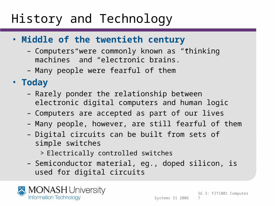
History and Technology
• Middle of the twentieth century– Computers were commonly known as “thinking machines”
and “electronic brains.”– Many people were fearful of them
• Today– Rarely ponder the relationship between electronic digital
computers and human logic– Computers are accepted as part of our lives– Many people, however, are still fearful of them– Digital circuits can be built from sets of simple switches
> Electrically controlled switches
– Semiconductor material, eg., doped silicon, is used for digital circuits
SG 3: FIT1001 Computer Systems S1 2006 8
History and Technology
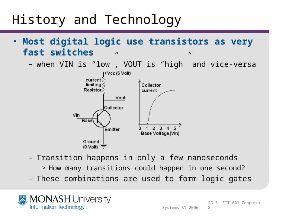
• Most digital logic use transistors as very fast switches
– when VIN is “low”, VOUT is “high” and vice-versa
– Transition happens in only a few nanoseconds> How many transitions could happen in one second?
– These combinations are used to form logic gates

SG 3: FIT1001 Computer Systems S1 2006 9
History and Technology
• Only two logical states– True/False, On/Off, 1/0– Generally 0-1 Volts indicates “Off”, 2-5 Volts indicates “On”
• Can Include several transistors for multiple inputs

www.monash.edu.au
Boolean Algebra

SG 3: FIT1001 Computer Systems S1 2006 11
Boolean Algebra
• Boolean algebra is a mathematical system for the manipulation of variables that can have one of two values.
– In formal logic, these values are “true” and “false.”– In digital systems, these values are “on” and “off,”
1 and 0, or “high” and “low.”
• Boolean expressions are created by performing operations on Boolean variables
– Common Boolean operators include AND, OR, NOT
SG 3: FIT1001 Computer Systems S1 2006 12
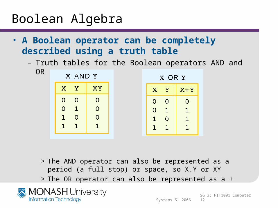
Boolean Algebra
• A Boolean operator can be completely described using a truth table
– Truth tables for the Boolean operators AND and OR
> The AND operator can also be represented as a period (a full stop) or space, so X.Y or XY
> The OR operator can also be represented as a +
SG 3: FIT1001 Computer Systems S1 2006 13
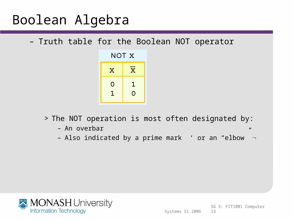
Boolean Algebra
– Truth table for the Boolean NOT operator
> The NOT operation is most often designated by:– An overbar– Also indicated by a prime mark ‘ or an “elbow”
SG 3: FIT1001 Computer Systems S1 2006 14
Boolean Algebra
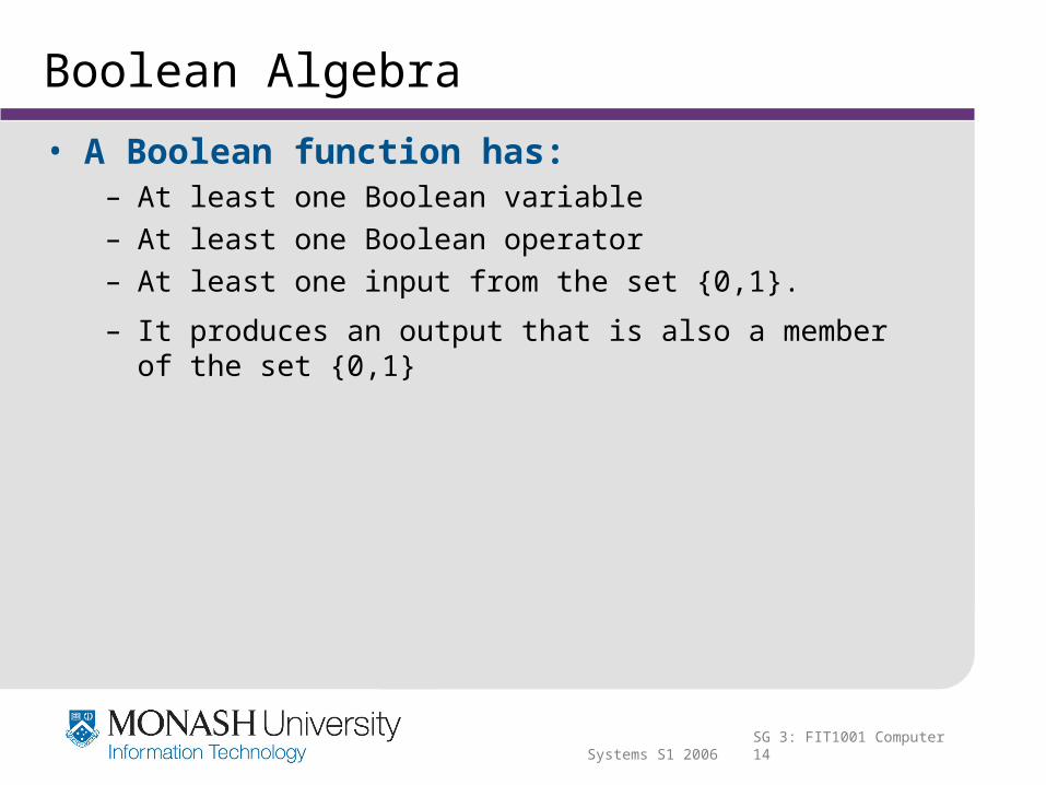
• A Boolean function has:– At least one Boolean variable– At least one Boolean operator– At least one input from the set {0,1}.
– It produces an output that is also a member of the set {0,1}

SG 3: FIT1001 Computer Systems S1 2006 15
Boolean Algebra
• The truth table for the Boolean function onthe right is below:
To make evaluation of the Boolean function easier, the truth table contains extra (shaded) columns to hold evaluations of subparts of the function

SG 3: FIT1001 Computer Systems S1 2006 16
Boolean Algebra
• As with common arithmetic, Boolean operations have rules of precedence
– The NOT operator has highest priority, followed by AND and then OR
> This is how we chose the (shaded) function subparts in our table

SG 3: FIT1001 Computer Systems S1 2006 17
Boolean Algebra
• Digital computers contain circuits that implement Boolean functions
– The simpler that we can make a Boolean function, the smaller the circuit that will result
– Simpler circuits are cheaper to build, consume less power, and run faster than complex circuits
• With this in mind– Always want to reduce our Boolean functions to their simplest
form– There are a number of Boolean identities that help us to do
this

SG 3: FIT1001 Computer Systems S1 2006 18
Boolean Algebra
• Most Boolean identities have an AND (product) form as well as an OR (sum) form
• The second group of Boolean identities should be familiar to you from your study of algebra

SG 3: FIT1001 Computer Systems S1 2006 19
Boolean Algebra
• The last group of Boolean identities are perhaps the most useful

SG 3: FIT1001 Computer Systems S1 2006 20
Boolean Algebra
• We can use Boolean identities to simplify the function:

SG 3: FIT1001 Computer Systems S1 2006 21
Boolean Algebra
• Sometimes it is more economical to build a circuit using the complement of a function (and complementing its result) than it is to implement the function directly
– DeMorgan’s law provides an easy way of finding the complement of a Boolean function.
– Recall DeMorgan’s law states
> DeMorgan’s law can be extended to any number of variables

SG 3: FIT1001 Computer Systems S1 2006 22
Boolean Algebra
– Replace each variable by its complement and change all ANDs to ORs and all ORs to ANDs
> Thus, we find the the complement of:
– Is:

SG 3: FIT1001 Computer Systems S1 2006 23
Boolean Algebra
• Through our exercises in simplifying Boolean expressions, we see that there are numerous ways of stating the same Boolean expression
– These “synonymous” forms are logically equivalent– Logically equivalent expressions have identical truth tables– In order to eliminate as much confusion as possible,
designers express Boolean functions in standardized or canonical form

SG 3: FIT1001 Computer Systems S1 2006 24
Boolean Algebra
• There are two canonical forms for Boolean expressions
– Sum-of-products and product-of-sums– Recall the Boolean product is the AND operation and the
Boolean sum is the OR operation– In the sum-of-products form, ANDed variables are ORed
together> For example:
– In the product-of-sums form, ORed variables are ANDed together
> For example:

SG 3: FIT1001 Computer Systems S1 2006 25
Boolean Algebra
• It is easy to convert a function to sum-of-products form using its truth table
– We are interested in the values of the variables that make the function true (=1)
– Using the truth table, we list the values of the variables that result in a true function value
– Each group of variables is then ORed together

SG 3: FIT1001 Computer Systems S1 2006 26
Boolean Algebra
• It is easy to convert a function to sum-of-products form using its truth table
– We are interested in the values of the variables that make the function true (=1)
– Using the truth table, we list the values of the variables that result in a true function value
– Each group of variables is then ORed together

www.monash.edu.au
Logic Gates and Truth Tables

SG 3: FIT1001 Computer Systems S1 2006 28
Logic Gates
• Logic Gates– The logic gate is the building brick of digital logic– A logic gate is an electronic device that produces a result
based on two or more input values> In reality, gates consist of one to six transistors, but digital
designers think of them as a single unit
– Integrated circuits contain collections of gates suited to a particular purpose

SG 3: FIT1001 Computer Systems S1 2006 29
Logic Gates
• The three simplest gates are the AND, OR, and NOT gates:
– They correspond directly to their respective Boolean operations, as you can see by their truth tables.

SG 3: FIT1001 Computer Systems S1 2006 30
Logic Gates
• Another very useful gate is the exclusive OR (XOR) gate
– The output of the XOR operation is true only when the values of the inputs differ

SG 3: FIT1001 Computer Systems S1 2006 31
Logic Gates
• NAND and NOR are two other very important gates
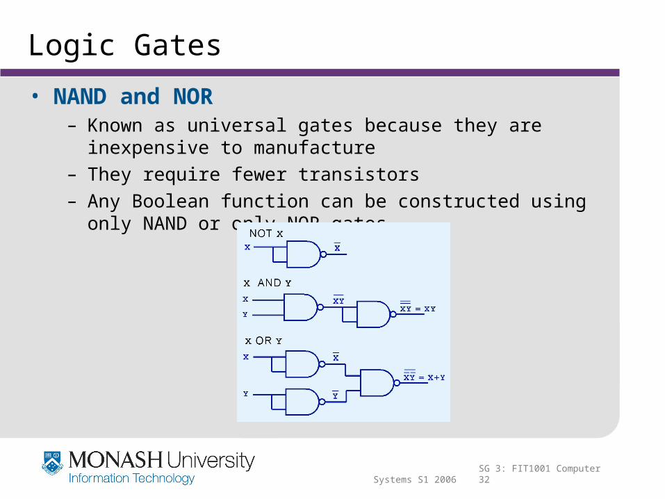
SG 3: FIT1001 Computer Systems S1 2006 32
Logic Gates
• NAND and NOR – Known as universal gates because they are inexpensive to
manufacture– They require fewer transistors– Any Boolean function can be constructed using only NAND or
only NOR gates

SG 3: FIT1001 Computer Systems S1 2006 33
Logic Gates
• Gates can have multiple inputs and more than one output
– A second output can be provided for the complement of the operation

SG 3: FIT1001 Computer Systems S1 2006 34
Logic Gates
• Designing Logic Circuits– Signal "z" must be 1 when signal "w" is 1 and either signal "x"
or signal "y" is 1. Signal "z" must also be 1 whenever signal "w" and signal "y" have different values
– Could solve this design problem by breaking up both of its sentences into smaller parts and selecting the appropriate logic gate to solve each part

SG 3: FIT1001 Computer Systems S1 2006 35
Logic Gates
– Truth table
W X Y W’ X+Y W’(X+Y) WY (W’(X+Y))+(WY)=Z
0 0 0 1 0 0 0 0
0 0 1 1 1 1 1 1
0 1 0 1 1 1 0 1
0 1 1 1 1 1 1 1
1 0 0 0 0 0 1 1
1 0 1 0 1 0 0 0
1 1 0 0 1 0 1 1
1 1 1 0 1 0 0 0

SG 3: FIT1001 Computer Systems S1 2006 36
Logic Gates
• The main thing to remember is that combinations of gates implement Boolean functions
– The circuit below implements the Boolean function:
www.monash.edu.au
Combinatorial Logic
SG 3: FIT1001 Computer Systems S1 2006 38
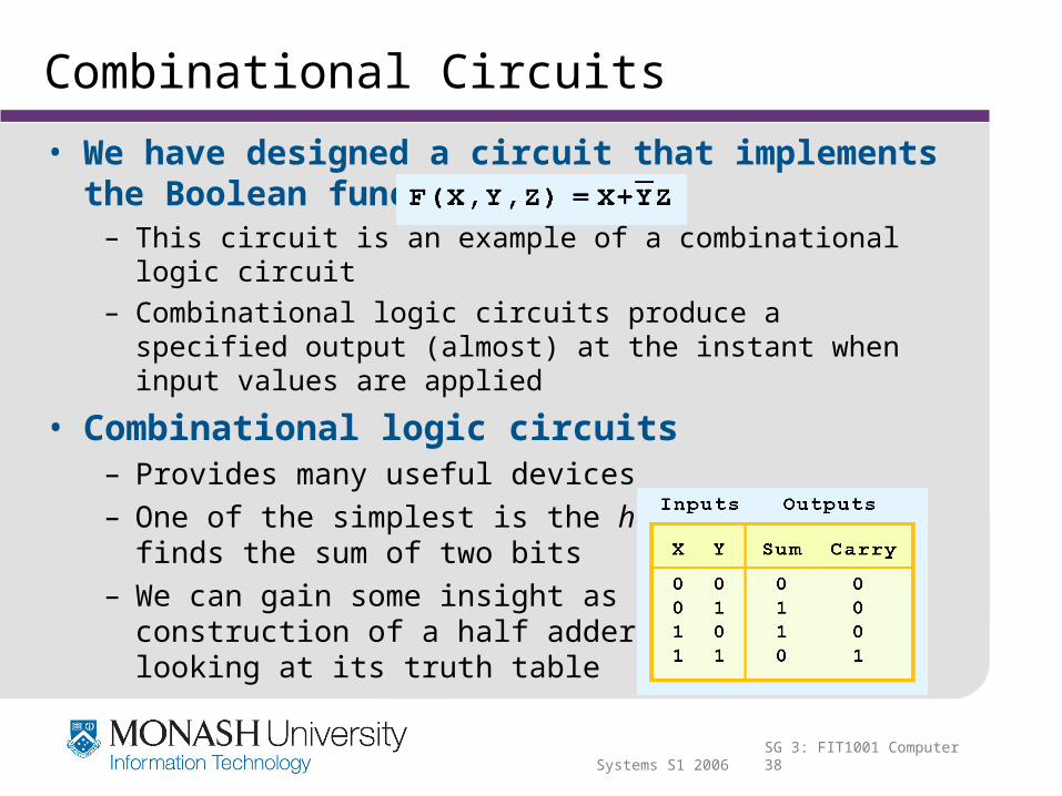
Combinational Circuits
• We have designed a circuit that implements the Boolean function:
– This circuit is an example of a combinational logic circuit– Combinational logic circuits produce a specified output
(almost) at the instant when input values are applied
• Combinational logic circuits– Provides many useful devices– One of the simplest is the half adder, which finds the sum
of two bits– We can gain some insight as to the
construction of a half adder by looking at its truth table

SG 3: FIT1001 Computer Systems S1 2006 39
Combinational Circuits
– As we see, the sum can be found using the XOR operation and the carry using the AND operation.

SG 3: FIT1001 Computer Systems S1 2006 40
Combinational Circuits
– We can change our half adder into to a full adder by including gates for processing the carry bit
– The truth table for a full adder is:

SG 3: FIT1001 Computer Systems S1 2006 41
Combinational Circuits
– How can we change the half adder (shown below left) to make it a full adder (shown below right)?

SG 3: FIT1001 Computer Systems S1 2006 42
Combinational Circuits
– Completed full adder

SG 3: FIT1001 Computer Systems S1 2006 43
Combinational Circuits
• Just as we combined half adders to make a full adder, full adders can connected in series
– The carry bit “ripples” from one adder to the next; hence, this configuration is called a ripple-carry adder

SG 3: FIT1001 Computer Systems S1 2006 44
Combinational Circuits
• Decoders are another important type of combinational circuit
– Useful in selecting a memory location according a binary value placed on the address lines of a memory bus
– Address decoders with n inputs can select any of 2n locations.

SG 3: FIT1001 Computer Systems S1 2006 45
Combinational Circuits
– This is what a 2-to-4 decoder looks like on the inside
If x = 0 and y = 1, which output line is enabled?

SG 3: FIT1001 Computer Systems S1 2006 46
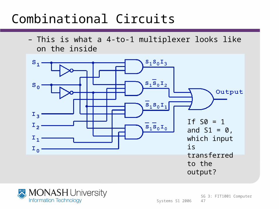
Combinational Circuits
• A multiplexer does just the opposite of a decoder– It selects a single output from several inputs.– The particular input chosen for output is determined by the
value of the multiplexer’s control lines
– To be able to select among n inputs, log2n control lines are needed.
SG 3: FIT1001 Computer Systems S1 2006 47
Combinational Circuits
– This is what a 4-to-1 multiplexer looks like on the inside
If S0 = 1 and S1 = 0, which input is transferred to the output?

www.monash.edu.au
Sequential Logic - Memory

SG 3: FIT1001 Computer Systems S1 2006 49
Sequential Circuits
• Combinational logic circuits are perfect for situations when we require the immediate application of a Boolean function to a set of inputs
– There are other times when we need a circuit to change its value with consideration to its current state as well as its inputs
– These circuits have to “remember” their current state
• Sequential logic circuits provide this functionality

SG 3: FIT1001 Computer Systems S1 2006 50
Sequential Circuits
• Sequential logic circuits require a means by which events can be sequenced
– State changes are controlled by clocks> A “clock” is a special circuit that sends electrical pulses through
a circuit
– Clocks produce electrical waveforms such as the one shown below.

SG 3: FIT1001 Computer Systems S1 2006 51
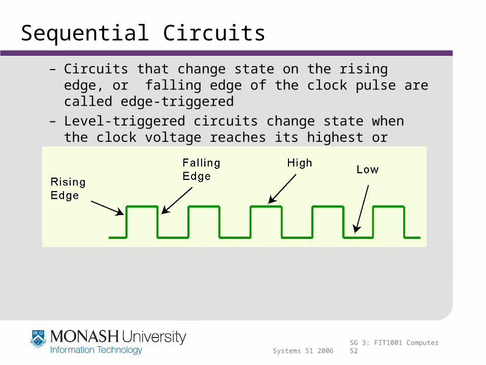
Sequential Circuits
– State changes occur in sequential circuits only when the clock ticks
– Circuits can change state on the rising edge, falling edge, or when the clock pulse reaches its highest voltage
SG 3: FIT1001 Computer Systems S1 2006 52
Sequential Circuits
– Circuits that change state on the rising edge, or falling edge of the clock pulse are called edge-triggered
– Level-triggered circuits change state when the clock voltage reaches its highest or lowest level

SG 3: FIT1001 Computer Systems S1 2006 53
Sequential Circuits
– To retain their state values, sequential circuits rely on feedback
– Feedback in digital circuits occurs when an output is looped back to the input
> Eg., If Q is 0 it will always be 0, if it is 1, it will always be 1

SG 3: FIT1001 Computer Systems S1 2006 54
Sequential Circuits
• SR flip-flop – You can see how feedback works by examining the most
basic sequential logic components, the SR flip-flop> The “SR” stands for set/reset
– The internals of an SR flip-flop are shown below, along with its block diagram

SG 3: FIT1001 Computer Systems S1 2006 55
Sequential Circuits
– The behavior of an SR flip-flop is described by a characteristic table
> Q(t) means the value of the output at time t
> Q(t+1) is the value of Q after the next clock pulse

SG 3: FIT1001 Computer Systems S1 2006 56
Sequential Circuits
– The SR flip-flop actually has three inputs: S, R, and its current output, Q
> Can construct a state table for this circuit
> Notice the two undefined values– When both S and R are 1, the – SR flip-flop is unstable

SG 3: FIT1001 Computer Systems S1 2006 57
Sequential Circuits
– If we can be sure that the inputs to an SR flip-flop will never both be 1
> Will never have an unstable circuit
> This may not always be the case
– The SR flip-flop can be modified to provide a stable state when both inputs are 1
This modified flip-flop is called a JK flip-flop
The “JK” is in honor of Jack Kilby.

SG 3: FIT1001 Computer Systems S1 2006 58
Sequential Circuits
– Below, left we see how an SR flip-flop can be modified to create a JK flip-flop
– The characteristic table indicates that the flip-flop is stable for all inputs
Note: Q and Q’ are reversed!

SG 3: FIT1001 Computer Systems S1 2006 59
Sequential Circuits
– Another modification of the SR flip-flop is the D flip-flop
> You will notice that the output of the flip-flop remains the same during subsequent clock pulses. The output changes only when the value of D changes

SG 3: FIT1001 Computer Systems S1 2006 60
Sequential Circuits
• D flip-flop – Is the fundamental circuit of computer memory – D flip-flops are usually illustrated using the block diagram

SG 3: FIT1001 Computer Systems S1 2006 61
Sequential Circuits
– A 4-bit register consisting of D flip-flops (right)
– Usually see its block diagraminstead (below)

SG 3: FIT1001 Computer Systems S1 2006 62
Sequential Circuits
• Binary counter – Another example of a sequential
circuit– The low-order bit is
complemented at each clock pulse
– Whenever it changes from 0 to 1the next bit is complemented, and so on through the other flip-flops

SG 3: FIT1001 Computer Systems S1 2006 63
Sequential Circuit Overview
• Sequential circuits have internal states as well as combinations of input and output logic
– The outputs are not set only by the combination of inputs> May also depend on the states left behind by previous inputs
Eg. Binary Counter

www.monash.edu.au
State Machines

SG 3: FIT1001 Computer Systems S1 2006 65
State Machines
• State Machines– Even relatively simple sequential
logic circuits can produce very complex state tables
– A better way to represent the sequence of states that may occur is to use a State Transition Table
> Each clock pulse causes a change of internal states based on the available combinatorial inputs
> Each state generates a new set of outputs
– A state machine diagram is displayed on the right

SG 3: FIT1001 Computer Systems S1 2006 66
State Machines
– State machines can be constructed to produce outputs produced by simple algorithms
– Speed is limited only by the clock rate– Often much faster than a software program– Inside a CPU, state machines are used to implement “hard-
wired” control units– Very complex control units use a ROM to generate the
combinatorial outputs for each state> These are said to be “micro-coded” systems

www.monash.edu.au
Designing Circuits

SG 3: FIT1001 Computer Systems S1 2006 68
Designing Circuits
• We have seen digital circuits from two points of view:
– Digital analysis: explores the relationship between a circuits inputs and its outputs
– Digital synthesis: creates logic diagrams using the values specified in a truth table
• Digital systems designers must also be mindful of the physical behaviors of circuits
– To include minute propagation delays that occur between the time when a circuit’s inputs are energized and when the output is accurate and stable

SG 3: FIT1001 Computer Systems S1 2006 69
Designing Circuits
• Digital designers rely on specialised software to create efficient circuits
– Thus, software is an enabler for the construction of better hardware
– Of course, software is in reality a collection of algorithms that could just as well be implemented in hardware
> Recall the Principle of Equivalence of Hardware and Software
– When implementing a simple, specialized algorithm and its execution speed must be as fast as possible, a hardware solution is often preferred
> This is the idea behind embedded systems, which are small special-purpose computers that we find in many everyday things
– Embedded systems require special programming that demands an understanding of the operation of digital circuits

SG 3: FIT1001 Computer Systems S1 2006 70
Next Week
• Study Guide 4– CPU Internal Bus Organisation