Embed Size (px)
Citation preview
CD-C606/1900,CP-C606/1900
– 1 –
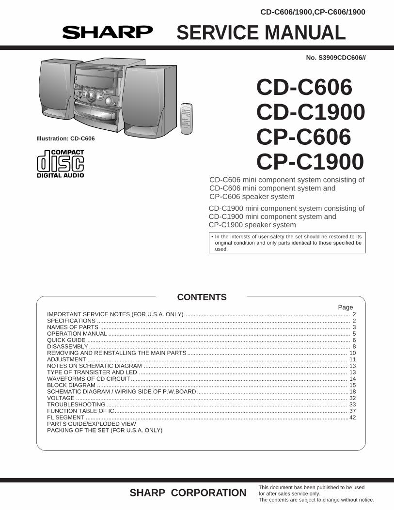
CD-C606CD-C1900CP-C606CP-C1900
• In the interests of user-safety the set should be restored to itsoriginal condition and only parts identical to those specified beused.
SERVICE MANUAL
SHARP CORPORATION
No. S3909CDC606//
This document has been published to be usedfor after sales service only.The contents are subject to change without notice.
CONTENTSPage
IMPORTANT SERVICE NOTES (FOR U.S.A. ONLY)....................................................................................................... 2SPECIFICATIONS ............................................................................................................................................................. 2NAMES OF PARTS ........................................................................................................................................................... 3OPERATION MANUAL ...................................................................................................................................................... 5QUICK GUIDE ................................................................................................................................................................... 6DISASSEMBLY .................................................................................................................................................................. 8REMOVING AND REINSTALLING THE MAIN PARTS ................................................................................................... 10ADJUSTMENT ................................................................................................................................................................. 11NOTES ON SCHEMATIC DIAGRAM .............................................................................................................................. 13TYPE OF TRANSISTER AND LED ................................................................................................................................. 13WAVEFORMS OF CD CIRCUIT ...................................................................................................................................... 14BLOCK DIAGRAM ........................................................................................................................................................... 15SCHEMATIC DIAGRAM / WIRING SIDE OF P.W.BOARD .............................................................................................. 18VOLTAGE ........................................................................................................................................................................ 32TROUBLESHOOTING ..................................................................................................................................................... 33FUNCTION TABLE OF IC................................................................................................................................................ 37FL SEGMENT ................................................................................................................................................................... 42PARTS GUIDE/EXPLODED VIEWPACKING OF THE SET (FOR U.S.A. ONLY)
CD-C606 mini component system consisting ofCD-C606 mini component system andCP-C606 speaker system
CD-C1900 mini component system consisting ofCD-C1900 mini component system andCP-C1900 speaker system
Illustration: CD-C606

CD-C606/1900,CP-C606/1900
– 2 –
FOR A COMPLETE DESCRIPTION OF THE OPERATION OF THIS UNIT, PLEASE REFERTO THE OPERATION MANUAL.
CD-C606/1900
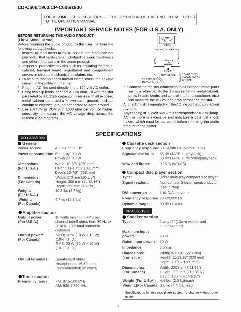
IMPORTANT SERVICE NOTES (FOR U.S.A. ONLY)BEFORE RETURNING THE AUDIO PRODUCT(Fire & Shock Hazard)Before returning the audio product to the user, perform thefollowing safety checks.1. Inspect all lead dress to make certain that leads are not
pinched or that hardware is not lodged between the chassisand other metal parts in the audio product.
2. Inspect all protective devices such as insulating materials,cabinet, terminal board, adjustment and compartmentcovers or shields, mechanical insulators etc.
3. To be sure that no shock hazard exists, check for leakagecurrent in the following manner.
* Plug the AC line cord directly into a 120 volt AC outlet.* Using two clip leads, connect a 1.5k ohm, 10 watt resistor
paralleled by a 0.15µF capacitor in series with all exposedmetal cabinet parts and a known earth ground, such asconduit or electrical ground connected to earth ground.
* Use a VTVM or VOM with 1000 ohm per volt, or higher,sensitivity to measure the AC voltage drop across theresistor (See diagram).
* Connect the resistor connection to all exposed metal partshaving a return path to the chassis (antenna, metal cabinet,screw heads, knobs and control shafts, escutcheon, etc.)and measure the AC voltage drop across the resistor.
All check must be repeated with the AC line cord plug connectionreversed.Any reading of 0.3 volt RMS (this corresponds to 0.2 milliamp.AC.) or more is excessive and indicates a potential shockhazard which must be corrected before returning the audioproduct to the owner.
SPECIFICATIONS
AC SCALE
VTVM
1.5k ohms10W
0.15µF
TEST PROBE
TO EXPOSEDMETAL PARTS
CONNECT TOKNOWN EARTHGROUND
GeneralPower source: AC 120 V, 60 Hz
Power consumption: Stand-by; 0.3 WPower on; 40 W
Dimensions: Width; 10-5/8" (270 mm)Height; 11-13/16" (300 mm)Depth; 13-7/8" (353 mm)
Weight: 10.3 lbs (4.7 kg)
Amplifier sectionOutput power: 10 watts minimum RMS per
channel into 8 ohms from 80 Hz to20 kHz, 10% total harmonicdistortion
Output terminals: Speakers; 8 ohmsHeadphones; 16-50 ohms(recommended; 32 ohms)
Tuner sectionFrequency range: FM; 87.5-108 MHz
AM; 530-1,720 kHz
Cassette deck sectionFrequency response: 50-14,000 Hz (Normal tape)
Signal/noise ratio: 55 dB (TAPE 1, playback)50 dB (TAPE 2, recording/playback)
Wow and flutter: 0.15 % (WRMS)
Compact disc player sectionType: 3-disc multi-play compact disc player
Signal readout: Non-contact, 3-beam semiconductorlaser pickup
D/A converter: 1-bit D/A converter
Frequency response: 20 -20,000 Hz
Dynamic range: 90 dB (1 kHz)
Speaker sectionType: 2-way [4” (10cm) woofer and
super tweeter]
Maximum inputpower: 20 W
Rated input power: 10 W
Impedance: 8 ohms
Dimensions: Width; 8-11/16" (220 mm)Height; 11-13/16" (300 mm)Depth; 7-1/16" (180 mm)
Weight:(For U.S.A.) 4.4 lbs. (2.0 kg)/each
(For U.S.A.)
(For U.S.A.)
(For U.S.A.)
Dimensions: Width; 270 mm (10-5/8")Height; 300 mm (11-13/16")Depth; 353 mm (13-7/8")
Weight: 4.7 kg (10.3 lbs)
Output power: MPO; 36 W (18 W + 18 W)(10% T.H.D.)RMS; 20 W (10 W + 10 W)(10% T.H.D.)
Dimensions: Width; 220 mm (8-11/16")Height; 300 mm (11-13/16")Depth; 180 mm (7-1/16")
Weight:(For Canada) 2.0 kg (4.4 lbs.)/each
(For Canada)
(For U.S.A.)
(For Canada)
(For Canada)
(For Canada)
CP-C606/1900
Specifications for this model are subject to change without priornotice.
CD-C606/1900,CP-C606/1900
– 2 –
FOR A COMPLETE DESCRIPTION OF THE OPERATION OF THIS UNIT, PLEASE REFERTO THE OPERATION MANUAL.
CD-C606/1900
IMPORTANT SERVICE NOTES (FOR U.S.A. ONLY)BEFORE RETURNING THE AUDIO PRODUCT(Fire & Shock Hazard)Before returning the audio product to the user, perform thefollowing safety checks.1. Inspect all lead dress to make certain that leads are not
pinched or that hardware is not lodged between the chassisand other metal parts in the audio product.
2. Inspect all protective devices such as insulating materials,cabinet, terminal board, adjustment and compartmentcovers or shields, mechanical insulators etc.
3. To be sure that no shock hazard exists, check for leakagecurrent in the following manner.
* Plug the AC line cord directly into a 120 volt AC outlet.* Using two clip leads, connect a 1.5k ohm, 10 watt resistor
paralleled by a 0.15µF capacitor in series with all exposedmetal cabinet parts and a known earth ground, such asconduit or electrical ground connected to earth ground.
* Use a VTVM or VOM with 1000 ohm per volt, or higher,sensitivity to measure the AC voltage drop across theresistor (See diagram).
* Connect the resistor connection to all exposed metal partshaving a return path to the chassis (antenna, metal cabinet,screw heads, knobs and control shafts, escutcheon, etc.)and measure the AC voltage drop across the resistor.
All check must be repeated with the AC line cord plug connectionreversed.Any reading of 0.3 volt RMS (this corresponds to 0.2 milliamp.AC.) or more is excessive and indicates a potential shockhazard which must be corrected before returning the audioproduct to the owner.
SPECIFICATIONS
AC SCALE
VTVM
1.5k ohms10W
0.15µF
TEST PROBE
TO EXPOSEDMETAL PARTS
CONNECT TOKNOWN EARTHGROUND
GeneralPower source: AC 120 V, 60 Hz
Power consumption: Stand-by; 0.3 WPower on; 40 W
Dimensions: Width; 10-5/8" (270 mm)Height; 11-13/16" (300 mm)Depth; 13-7/8" (353 mm)
Weight: 10.3 lbs (4.7 kg)
Amplifier sectionOutput power: 10 watts minimum RMS per
channel into 8 ohms from 80 Hz to20 kHz, 10% total harmonicdistortion
Output terminals: Speakers; 8 ohmsHeadphones; 16-50 ohms(recommended; 32 ohms)
Tuner sectionFrequency range: FM; 87.5-108 MHz
AM; 530-1,720 kHz
Cassette deck sectionFrequency response: 50-14,000 Hz (Normal tape)
Signal/noise ratio: 55 dB (TAPE 1, playback)50 dB (TAPE 2, recording/playback)
Wow and flutter: 0.15 % (WRMS)
Compact disc player sectionType: 3-disc multi-play compact disc player
Signal readout: Non-contact, 3-beam semiconductorlaser pickup
D/A converter: 1-bit D/A converter
Frequency response: 20 -20,000 Hz
Dynamic range: 90 dB (1 kHz)
Speaker sectionType: 2-way [4” (10cm) woofer and
super tweeter]
Maximum inputpower: 20 W
Rated input power: 10 W
Impedance: 8 ohms
Dimensions: Width; 8-11/16" (220 mm)Height; 11-13/16" (300 mm)Depth; 7-1/16" (180 mm)
Weight:(For U.S.A.) 4.4 lbs. (2.0 kg)/each
(For U.S.A.)
(For U.S.A.)
(For U.S.A.)
Dimensions: Width; 270 mm (10-5/8")Height; 300 mm (11-13/16")Depth; 353 mm (13-7/8")
Weight: 4.7 kg (10.3 lbs)
Output power: MPO; 36 W (18 W + 18 W)(10% T.H.D.)RMS; 20 W (10 W + 10 W)(10% T.H.D.)
Dimensions: Width; 220 mm (8-11/16")Height; 300 mm (11-13/16")Depth; 180 mm (7-1/16")
Weight:(For Canada) 2.0 kg (4.4 lbs.)/each
(For Canada)
(For U.S.A.)
(For Canada)
(For Canada)
(For Canada)
CP-C606/1900
Specifications for this model are subject to change without priornotice.
CD-C606/1900,CP-C606/1900
– 3 –
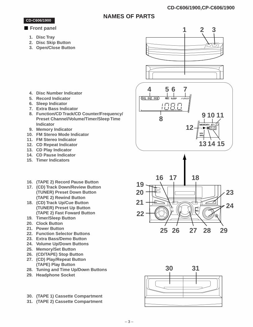
NAMES OF PARTSCD-C606/1900
4. Disc Number Indicator5. Record Indicator6. Sleep Indicator7. Extra Bass Indicator8. Function/CD Track/CD Counter/Frequency/
Preset Channel/Volume/Timer/Sleep TimeIndicator
9. Memory Indicator10. FM Stereo Mode Indicator11. FM Stereo Indicator12. CD Repeat Indicator13. CD Play Indicator14. CD Pause Indicator15. Timer Indicators
16. (TAPE 2) Record Pause Button17. (CD) Track Down/Review Button
(TUNER) Preset Down Button(TAPE 2) Rewind Button
18. (CD) Track Up/Cue Button(TUNER) Preset Up Button(TAPE 2) Fast Foward Button
19. Timer/Sleep Button20. Clock Button21. Power Button22. Function Selector Buttons23. Extra Bass/Demo Button24. Volume Up/Down Buttons25. Memory/Set Button26. (CD/TAPE) Stop Button27. (CD) Play/Repeat Button
(TAPE) Play Button28. Tuning and Time Up/Down Buttons29. Headphone Socket
Front panel
1. Disc Tray2. Disc Skip Button3. Open/Close Button
30. (TAPE 1) Cassette Compartment31. (TAPE 2) Cassette Compartment
1 2 3 X-BASS
kHzMHz
SLEEP
STMEMORY
REC
4 5 6 7
8
13 14
9 10 11
12
19
21
25
16
23
2422
20
27
17
26
18
28 29
30 31
1 2 3
15
CD-C606/1900,CP-C606/1900
– 4 –
CD-C606/1900
2
1 3
1
1
2 8
10
9
1112
22
3
4567
13
18192021
7
4
5
6
14 15 16 17
CP-C606/1900
CD-C606/1900
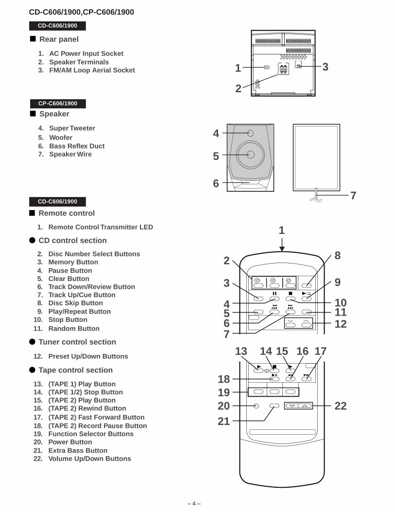
Rear panel
1. AC Power Input Socket2. Speaker Terminals3. FM/AM Loop Aerial Socket
Remote control
1. Remote Control Transmitter LED
CD control section
2. Disc Number Select Buttons3. Memory Button4. Pause Button5. Clear Button6. Track Down/Review Button7. Track Up/Cue Button8. Disc Skip Button9. Play/Repeat Button
10. Stop Button11. Random Button
Tuner control section
12. Preset Up/Down Buttons
Tape control section
13. (TAPE 1) Play Button14. (TAPE 1/2) Stop Button15. (TAPE 2) Play Button16. (TAPE 2) Rewind Button17. (TAPE 2) Fast Forward Button18. (TAPE 2) Record Pause Button19. Function Selector Buttons20. Power Button21. Extra Bass Button22. Volume Up/Down Buttons
Speaker
4. Super Tweeter5. Woofer6. Bass Reflex Duct7. Speaker Wire
CD-C606/1900,CP-C606/1900
– 5 –
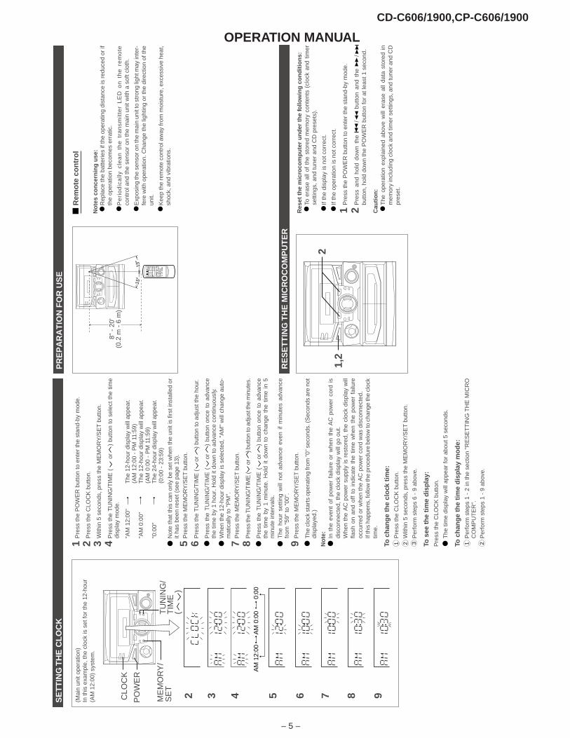
OPERATION MANUAL
AM
0:0
0A
M 1
2:00
0:00
(Mai
n un
it op
erat
ion)
In th
is e
xam
ple,
the
cloc
k is
set
for
the
12-h
our
(AM
12:
00)
syst
em.
2 3 5 6 7 9PO
WE
R
ME
MO
RY
/S
ET
CLO
CK
TU
NIN
G/
TIM
E(
)
1P
ress
the
PO
WE
R b
utto
n to
ent
er th
e st
and-
by m
ode.
2P
ress
the
CLO
CK
but
ton.
3W
ithin
5 s
econ
ds, p
ress
the
ME
MO
RY
/SE
T b
utto
n.
4P
ress
the
TU
NIN
G/T
IME
(
or
) bu
tton
to s
elec
t th
e tim
edi
spla
y m
ode.
"AM
12:
00"
The
12-
hour
dis
play
will
app
ear.
(AM
12:
00 -
PM
11:
59)
"AM
0:0
0"T
he 1
2-ho
ur d
ispl
ay w
ill a
ppea
r.(A
M 0
:00
- P
M 1
1:59
)"0
:00"
The
24-
hour
dis
play
will
app
ear.
(0:0
0 -
23:5
9)
Not
e th
at th
is c
an o
nly
be s
et w
hen
the
unit
is fi
rst i
nsta
lled
orit
has
been
res
et (
see
page
13)
.5
Pre
ss th
e M
EM
OR
Y/S
ET
but
ton.
6P
ress
the
TU
NIN
G/T
IME
( o
r )
butto
n to
adj
ust t
he h
our.
Pre
ss t
he T
UN
ING
/TIM
E (
or
) bu
tton
once
to
adva
nce
the
time
by 1
hou
r. H
old
it do
wn
to a
dvan
ce c
ontin
uous
ly.
Whe
n th
e 12
-hou
r di
spla
y is
sel
ecte
d, "
AM
" w
ill c
hang
e au
to-
mat
ical
ly to
"P
M".
7P
ress
the
ME
MO
RY
/SE
T b
utto
n.
8P
ress
the
TU
NIN
G/T
IME
( o
r ) b
utto
n to
adj
ust t
he m
inut
es.
Pre
ss t
he T
UN
ING
/TIM
E (
or
) bu
tton
once
to
adva
nce
the
time
by 1
min
ute.
Hol
d it
dow
n to
cha
nge
the
time
in 5
min
ute
inte
rval
s.T
he h
our
setti
ng w
ill n
ot a
dvan
ce e
ven
if m
inut
es a
dvan
cefr
om "
59"
to "
00".
9P
ress
the
ME
MO
RY
/SE
T b
utto
n.
The
clo
ck s
tart
s op
erat
ing
from
"0" s
econ
ds. (
Sec
onds
are
not
disp
laye
d.)
No
te:
In t
he e
vent
of
pow
er f
ailu
re o
r w
hen
the
AC
pow
er c
ord
isdi
scon
nect
ed, t
he c
lock
dis
play
will
go
out.
Whe
n th
e A
C p
ower
sup
ply
is r
esto
red,
the
clo
ck d
ispl
ay w
illfla
sh o
n an
d of
f to
ind
icat
e th
e tim
e w
hen
the
pow
er f
ailu
reoc
curr
ed o
r w
hen
the
AC
pow
er c
ord
was
dis
conn
ecte
d.If
this
hap
pens
, fol
low
the
proc
edur
e be
low
to c
hang
e th
e cl
ock
time.
To c
han
ge
the
clo
ck t
ime:
Pre
ss th
e C
LOC
K b
utto
n.
With
in 5
sec
onds
, pre
ss th
e M
EM
OR
Y/S
ET
but
ton.
Per
form
ste
ps 6
- 9
abo
ve.
To s
ee t
he
tim
e d
isp
lay:
Pre
ss th
e C
LOC
K b
utto
n.
The
tim
e di
spla
y w
ill a
ppea
r fo
r ab
out 5
sec
onds
.
To c
han
ge
the
tim
e d
isp
lay
mo
de:
Per
form
ste
ps 1
- 2
in th
e se
ctio
n "R
ES
ET
TIN
G T
HE
MIC
RO
CO
MP
UT
ER
".P
erfo
rm s
teps
1 -
9 a
bove
.
SE
TT
ING
TH
E C
LO
CK
84
1 2 3 1 2
PR
EP
AR
AT
ION
FO
R U
SE
Rem
ote
co
ntr
ol
No
tes
con
cern
ing
use
:R
epla
ce th
e ba
tterie
s if
the
oper
atin
g di
stan
ce is
red
uced
or
ifth
e op
erat
ion
beco
mes
err
atic
.
Pe
rio
dic
ally
cle
an
th
e t
ran
smit
ter
LE
D o
n t
he
re
mo
teco
ntro
l and
the
sens
or o
n th
e m
ain
unit
with
a s
oft c
loth
.
Exp
osin
g th
e se
nsor
on
the
mai
n un
it to
str
ong
light
may
inte
r-fe
re w
ith o
pera
tion.
Cha
nge
the
light
ing
or th
e di
rect
ion
of th
eun
it.
Kee
p th
e re
mot
e co
ntro
l aw
ay fr
om m
oist
ure,
exc
essi
ve h
eat,
shoc
k, a
nd v
ibra
tions
.
151515
1
8" -
20'
(0.2
m -
6 m
)
RE
SE
TT
ING
TH
E M
ICR
OC
OM
PU
TE
R
Res
et t
he
mic
roco
mp
ute
r u
nd
er t
he
follo
win
g c
on
dit
ion
s:To
era
se a
ll of
the
sto
red
mem
ory
cont
ents
(cl
ock
and
timer
setti
ngs,
and
tune
r an
d C
D p
rese
ts).
If th
e di
spla
y is
not
cor
rect
.
If th
e op
erat
ion
is n
ot c
orre
ct.
1P
ress
the
PO
WE
R b
utto
n to
ent
er th
e st
and-
by m
ode.
2P
ress
and
hol
d do
wn
the
/ b
utto
n an
d th
e /
butto
n, h
old
dow
n th
e P
OW
ER
but
ton
for
at le
ast 1
sec
ond.
Cau
tio
n:
The
ope
ratio
n ex
plai
ned
abov
e w
ill e
rase
all
data
sto
red
inm
emor
y in
clud
ing
cloc
k an
d tim
er s
ettin
gs, a
nd tu
ner
and
CD
pres
et.
1,2
2

CD-C606/1900,CP-C606/1900
– 6 –
QUICK GUIDE
1
VO
LUM
E
VO
LUM
E
1515
LEFT
RIGH
T
SPEA
KERS
RATE
D SP
EAKE
R IM
PEDA
NCE:
8 OH
MS
MIN
.
PO
WE
R
PO
WE
R
X-B
AS
S
X-BA
SS/D
EM
O
1
MIN
I CO
MP
ON
EN
TS
YS
TE
MC
D-C
606
Qu
ick-
Gu
ide
Gu
ía r
ápid
a
Pre
par
atio
n f
or
use
Pre
par
ació
n p
ara
su u
so
A
C 1
20 V
, 60
Hz
12
0 V
de
CA
, 60
Hz
Left
spea
ker
Alta
voz
izqu
ierd
o
A
M L
oop
Ant
enna
A
nten
a de
cua
dro
deA
M
F
M A
nten
na
A
nten
a de
FM
Bla
ck
Neg
ro
Red
Roj
oB
lack
Neg
ro
Red
Roj
o
Turn
ing
th
e p
ow
er o
n a
nd
off
Co
nex
ión
y d
esco
nex
ión
de
la a
limen
taci
ón
Rem
ote
co
ntr
ol
Co
ntr
ol r
emo
toR
emot
e S
enso
r
Sen
sor
rem
ote
2
“AA
” ba
tterie
s
D
os p
ilas
“AA
”
8" -
20
' (0.
2m -
6m
)
0,2m
- 6
m
B
atte
ries
are
not
incl
uded
.
La
s pi
las
no e
stán
incl
uida
s.
So
un
d c
on
tro
lC
on
tro
l del
so
nid
o
V
olum
e
Vo
lum
en
E
xtra
-BA
SS
G
rave
s ex
tra
Rig
ht s
peak
er
Alta
voz
dere
cho
ST
FM
ST
ER
OF
M M
ON
OA
M
TA
PE
1T
AP
E 2
TA
PE
2
REC
PAUS
E
OPE
N/C
LOSE
OPE
N/C
LOSE
TU
NIN
G/T
IME
TAPE
(1 2)
C D
TUNER (BAND)
TAPE
(1 2)
C D
TUNER (BAND)
TAPE
(1 2)
C D
TUNER (BAND)
TAPE
(1 2)
C D
TUNER (BAND)
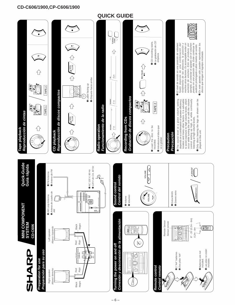
Tap
e p
layb
ack
Rep
rod
ucc
ión
de
cin
tas
Rec
ord
ing
fro
m C
Ds
Gra
bac
ión
de
dis
cos
com
pac
tos
L
oa
d t
he
dis
c to
be
reco
rded
.
In
trod
uzca
el d
isco
que
va a
gra
bar.
C
D r
ecor
ding
sta
rts.
La
gra
baci
ón d
e C
Dem
piez
a.
Rad
io o
per
atio
nF
un
cio
nam
ien
to d
e la
rad
io
T
he
so
un
d l
eve
l a
t a
giv
en
vo
lum
e s
ett
ing
depe
nds
on a
com
bina
tion
of s
peak
er e
ffici
ency
,lo
catio
n an
d m
any
othe
r fa
ctor
s. I
t is
adv
isab
leto
avo
id e
xpos
ure
to h
igh
volu
me
leve
ls,
whi
choc
cur
whi
le t
urni
ng t
he u
nit
on w
ith t
he v
olum
eco
ntr
ol
sett
ing
up
hig
h,
or
wh
ile c
on
tinu
ally
liste
ning
at h
igh
volu
me
leve
ls.
O
nly
disc
s be
arin
g th
e lo
go a
s sh
own
can
bepl
ayed
in th
is u
nit.
Pre
cau
tio
nP
reca
uci
ón
E
l niv
el d
e so
nido
en
una
posi
ción
de
volu
men
fija
do
de
pe
nd
e d
e u
na
co
mb
ina
ció
n d
el
rend
imie
nto
de l
as a
ltavo
ces,
la
posi
ción
ym
ucho
s ot
ros
fact
ores
. Es
acon
seja
ble
evita
r un
aum
ento
de
volu
men
. E
sto
se p
rodu
ce,
por
ejem
plo,
al c
onec
tar
el a
para
to c
on e
l vol
umen
pues
to e
n un
a po
sici
ón a
lta. E
vite
con
tinua
r la
audi
ción
pro
long
ada
a al
tos
nive
les
de s
onid
o.
En
este
apa
rato
sól
o pu
eden
rep
rodu
cirs
e lo
sdi
scos
que
teng
an e
l log
otip
o m
ostra
do.
La
bel f
acin
g up
E
tique
ta h
acia
arr
iba
CD
pla
ybac
kR
epro
du
cció
n d
e d
isco
s co
mp
acto
s
CD-C606/1900,CP-C606/1900
– 7 –
1
VO
LUM
E
VO
LUM
E
1515
LEFT
RIGH
T
SPEA
KERS
RATE
D SP
EAKE
R IM
PEDA
NCE:
8 OH
MS
MIN
.
PO
WE
R
PO
WE
R
X-B
AS
S
X-BA
SS/D
EM
O
1
MIN
I CO
MP
ON
EN
TS
YS
TE
MC
D-C
1900
Qu
ick-
Gu
ide
Gu
ía r
ápid
a
Pre
par
atio
n f
or
use
Pre
par
ació
n p
ara
su u
so
A
C 1
20 V
, 60
Hz
12
0 V
de
CA
, 60
Hz
Left
spea
ker
Alta
voz
izqu
ierd
o
A
M L
oop
Ant
enna
A
nten
a de
cua
dro
deA
M
F
M A
nten
na
A
nten
a de
FM
Bla
ck
Neg
ro
Red
Roj
oB
lack
Neg
ro
Red
Roj
o
Turn
ing
th
e p
ower
on
an
d o
ffC
on
exió
n y
des
con
exió
n d
e la
alim
enta
ció
n
Rem
ote
co
ntr
ol
Co
ntr
ol r
emo
toR
emot
e S
enso
r
Sen
sor
rem
ote
2
“AA
” ba
tterie
s
D
os p
ilas
“AA
”
8" -
20
' (0.
2m -
6m
)
0,2m
- 6
m
B
atte
ries
are
not
incl
uded
.
La
s pi
las
no e
stán
incl
uida
s.
So
un
d c
on
tro
lC
on
tro
l del
so
nid
o
V
olum
e
Vo
lum
en
E
xtra
-BA
SS
G
rave
s ex
tra
Rig
ht s
peak
er
Alta
voz
dere
cho
ST
FM
ST
ER
OF
M M
ON
OA
M
TA
PE
1T
AP
E 2
TA
PE
2
REC
PAUS
E
OPE
N/C
LOSE
OPE
N/C
LOSE
TU
NIN
G/T
IME
TAPE
(1 2)
C D
TUNER (BAND)
TAPE
(1 2)
C D
TUNER (BAND)
TAPE
(1 2)
C D
TUNER (BAND)
TAPE
(1 2)
C D
TUNER (BAND)
Tap
e p
layb
ack
Rep
rod
ucc
ión
de
cin
tas
Rec
ord
ing
fro
m C
Ds
Gra
bac
ión
de
dis
cos
com
pac
tos
L
oa
d t
he
dis
c to
be
reco
rded
.
In
trod
uzca
el d
isco
que
va a
gra
bar.
C
D r
ecor
ding
sta
rts.
La
gra
baci
ón d
e C
Dem
piez
a.
Rad
io o
per
atio
nF
un
cio
nam
ien
to d
e la
rad
io
T
he
so
un
d l
eve
l a
t a
giv
en
vo
lum
e s
ett
ing
depe
nds
on a
com
bina
tion
of s
peak
er e
ffici
ency
,lo
catio
n an
d m
any
othe
r fa
ctor
s. I
t is
adv
isab
leto
avo
id e
xpos
ure
to h
igh
volu
me
leve
ls,
whi
choc
cur
whi
le t
urni
ng t
he u
nit
on w
ith t
he v
olum
eco
ntr
ol
sett
ing
up
hig
h,
or
wh
ile c
on
tinu
ally
liste
ning
at h
igh
volu
me
leve
ls.
O
nly
disc
s be
arin
g th
e lo
go a
s sh
own
can
bepl
ayed
in th
is u
nit.
Pre
cau
tio
nP
reca
uci
ón
E
l niv
el d
e so
nido
en
una
posi
ción
de
volu
men
fija
do
de
pe
nd
e d
e u
na
co
mb
ina
ció
n d
el
rend
imie
nto
de l
as a
ltavo
ces,
la
posi
ción
ym
ucho
s ot
ros
fact
ores
. Es
acon
seja
ble
evita
r un
aum
ento
de
volu
men
. E
sto
se p
rodu
ce,
por
ejem
plo,
al c
onec
tar
el a
para
to c
on e
l vol
umen
pues
to e
n un
a po
sici
ón a
lta. E
vite
con
tinua
r la
audi
ción
pro
long
ada
a al
tos
nive
les
de s
onid
o.
En
este
apa
rato
sól
o pu
eden
rep
rodu
cirs
e lo
sdi
scos
que
teng
an e
l log
otip
o m
ostra
do.
La
bel f
acin
g up
E
tique
ta h
acia
arr
iba
CD
pla
ybac
kR
epro
du
cció
n d
e d
isco
s co
mp
acto
s
CD-C606/1900,CP-C606/1900
– 6 –
QUICK GUIDE
1
VO
LUM
E
VO
LUM
E
1515
LEFT
RIGH
T
SPEA
KERS
RATE
D SP
EAKE
R IM
PEDA
NCE:
8 OH
MS
MIN
.
PO
WE
R
PO
WE
R
X-B
AS
S
X-BA
SS/D
EM
O
1
MIN
I CO
MP
ON
EN
TS
YS
TE
MC
D-C
606
Qu
ick-
Gu
ide
Gu
ía r
ápid
a
Pre
par
atio
n f
or
use
Pre
par
ació
n p
ara
su u
so
A
C 1
20 V
, 60
Hz
12
0 V
de
CA
, 60
Hz
Left
spea
ker
Alta
voz
izqu
ierd
o
A
M L
oop
Ant
enna
A
nten
a de
cua
dro
deA
M
F
M A
nten
na
A
nten
a de
FM
Bla
ck
Neg
ro
Red
Roj
oB
lack
Neg
ro
Red
Roj
o
Turn
ing
th
e p
ow
er o
n a
nd
off
Co
nex
ión
y d
esco
nex
ión
de
la a
limen
taci
ón
Rem
ote
co
ntr
ol
Co
ntr
ol r
emo
toR
emot
e S
enso
r
Sen
sor
rem
ote
2
“AA
” ba
tterie
s
D
os p
ilas
“AA
”
8" -
20
' (0.
2m -
6m
)
0,2m
- 6
m
B
atte
ries
are
not
incl
uded
.
La
s pi
las
no e
stán
incl
uida
s.
So
un
d c
on
tro
lC
on
tro
l del
so
nid
o
V
olum
e
Vo
lum
en
E
xtra
-BA
SS
G
rave
s ex
tra
Rig
ht s
peak
er
Alta
voz
dere
cho
ST
FM
ST
ER
OF
M M
ON
OA
M
TA
PE
1T
AP
E 2
TA
PE
2
REC
PAUS
E
OPE
N/C
LOSE
OPE
N/C
LOSE
TU
NIN
G/T
IME
TAPE
(1 2)
C D
TUNER (BAND)
TAPE
(1 2)
C D
TUNER (BAND)
TAPE
(1 2)
C D
TUNER (BAND)
TAPE
(1 2)
C D
TUNER (BAND)
Tap
e p
layb
ack
Rep
rod
ucc
ión
de
cin
tas
Rec
ord
ing
fro
m C
Ds
Gra
bac
ión
de
dis
cos
com
pac
tos
L
oa
d t
he
dis
c to
be
reco
rded
.
In
trod
uzca
el d
isco
que
va a
gra
bar.
C
D r
ecor
ding
sta
rts.
La
gra
baci
ón d
e C
Dem
piez
a.
Rad
io o
per
atio
nF
un
cio
nam
ien
to d
e la
rad
io
T
he
so
un
d l
eve
l a
t a
giv
en
vo
lum
e s
ett
ing
depe
nds
on a
com
bina
tion
of s
peak
er e
ffici
ency
,lo
catio
n an
d m
any
othe
r fa
ctor
s. I
t is
adv
isab
leto
avo
id e
xpos
ure
to h
igh
volu
me
leve
ls,
whi
choc
cur
whi
le t
urni
ng t
he u
nit
on w
ith t
he v
olum
eco
ntr
ol
sett
ing
up
hig
h,
or
wh
ile c
on
tinu
ally
liste
ning
at h
igh
volu
me
leve
ls.
O
nly
disc
s be
arin
g th
e lo
go a
s sh
own
can
bepl
ayed
in th
is u
nit.
Pre
cau
tio
nP
reca
uci
ón
E
l niv
el d
e so
nido
en
una
posi
ción
de
volu
men
fija
do
de
pe
nd
e d
e u
na
co
mb
ina
ció
n d
el
rend
imie
nto
de l
as a
ltavo
ces,
la
posi
ción
ym
ucho
s ot
ros
fact
ores
. Es
acon
seja
ble
evita
r un
aum
ento
de
volu
men
. E
sto
se p
rodu
ce,
por
ejem
plo,
al c
onec
tar
el a
para
to c
on e
l vol
umen
pues
to e
n un
a po
sici
ón a
lta. E
vite
con
tinua
r la
audi
ción
pro
long
ada
a al
tos
nive
les
de s
onid
o.
En
este
apa
rato
sól
o pu
eden
rep
rodu
cirs
e lo
sdi
scos
que
teng
an e
l log
otip
o m
ostra
do.
La
bel f
acin
g up
E
tique
ta h
acia
arr
iba
CD
pla
ybac
kR
epro
du
cció
n d
e d
isco
s co
mp
acto
s

CD-C606/1900,CP-C606/1900
– 7 –
1
VO
LUM
E
VO
LUM
E
1515
LEFT
RIGH
T
SPEA
KERS
RATE
D SP
EAKE
R IM
PEDA
NCE:
8 OH
MS
MIN
.
PO
WE
R
PO
WE
R
X-B
AS
S
X-BA
SS/D
EM
O
1
MIN
I CO
MP
ON
EN
TS
YS
TE
MC
D-C
1900
Qu
ick-
Gu
ide
Gu
ía r
ápid
a
Pre
par
atio
n f
or
use
Pre
par
ació
n p
ara
su u
so
A
C 1
20 V
, 60
Hz
12
0 V
de
CA
, 60
Hz
Left
spea
ker
Alta
voz
izqu
ierd
o
A
M L
oop
Ant
enna
A
nten
a de
cua
dro
deA
M
F
M A
nten
na
A
nten
a de
FM
Bla
ck
Neg
ro
Red
Roj
oB
lack
Neg
ro
Red
Roj
o
Turn
ing
th
e p
ower
on
an
d o
ffC
on
exió
n y
des
con
exió
n d
e la
alim
enta
ció
n
Rem
ote
co
ntr
ol
Co
ntr
ol r
emo
toR
emot
e S
enso
r
Sen
sor
rem
ote
2
“AA
” ba
tterie
s
D
os p
ilas
“AA
”
8" -
20
' (0.
2m -
6m
)
0,2m
- 6
m
B
atte
ries
are
not
incl
uded
.
La
s pi
las
no e
stán
incl
uida
s.
So
un
d c
on
tro
lC
on
tro
l del
so
nid
o
V
olum
e
Vo
lum
en
E
xtra
-BA
SS
G
rave
s ex
tra
Rig
ht s
peak
er
Alta
voz
dere
cho
ST
FM
ST
ER
OF
M M
ON
OA
M
TA
PE
1T
AP
E 2
TA
PE
2
REC
PAUS
E
OPE
N/C
LOSE
OPE
N/C
LOSE
TU
NIN
G/T
IME
TAPE
(1 2)
C D
TUNER (BAND)
TAPE
(1 2)
C D
TUNER (BAND)
TAPE
(1 2)
C D
TUNER (BAND)
TAPE
(1 2)
C D
TUNER (BAND)
Tap
e p
layb
ack
Rep
rod
ucc
ión
de
cin
tas
Rec
ord
ing
fro
m C
Ds
Gra
bac
ión
de
dis
cos
com
pac
tos
L
oa
d t
he
dis
c to
be
reco
rded
.
In
trod
uzca
el d
isco
que
va a
gra
bar.
C
D r
ecor
ding
sta
rts.
La
gra
baci
ón d
e C
Dem
piez
a.
Rad
io o
per
atio
nF
un
cio
nam
ien
to d
e la
rad
io
T
he
so
un
d l
eve
l a
t a
giv
en
vo
lum
e s
ett
ing
depe
nds
on a
com
bina
tion
of s
peak
er e
ffici
ency
,lo
catio
n an
d m
any
othe
r fa
ctor
s. I
t is
adv
isab
leto
avo
id e
xpos
ure
to h
igh
volu
me
leve
ls,
whi
choc
cur
whi
le t
urni
ng t
he u
nit
on w
ith t
he v
olum
eco
ntr
ol
sett
ing
up
hig
h,
or
wh
ile c
on
tinu
ally
liste
ning
at h
igh
volu
me
leve
ls.
O
nly
disc
s be
arin
g th
e lo
go a
s sh
own
can
bepl
ayed
in th
is u
nit.
Pre
cau
tio
nP
reca
uci
ón
E
l niv
el d
e so
nido
en
una
posi
ción
de
volu
men
fija
do
de
pe
nd
e d
e u
na
co
mb
ina
ció
n d
el
rend
imie
nto
de l
as a
ltavo
ces,
la
posi
ción
ym
ucho
s ot
ros
fact
ores
. Es
acon
seja
ble
evita
r un
aum
ento
de
volu
men
. E
sto
se p
rodu
ce,
por
ejem
plo,
al c
onec
tar
el a
para
to c
on e
l vol
umen
pues
to e
n un
a po
sici
ón a
lta. E
vite
con
tinua
r la
audi
ción
pro
long
ada
a al
tos
nive
les
de s
onid
o.
En
este
apa
rato
sól
o pu
eden
rep
rodu
cirs
e lo
sdi
scos
que
teng
an e
l log
otip
o m
ostra
do.
La
bel f
acin
g up
E
tique
ta h
acia
arr
iba
CD
pla
ybac
kR
epro
du
cció
n d
e d
isco
s co
mp
acto
s
CD-C606/1900,CP-C606/1900
– 10 –
How to remove the turntable up/down/loadingmotor (See Fig. 10-3)1. Remove the screws (A1) x 2 pcs., to remove the turntable
up/down/loading motor.
How to remove the pickup (See Fig. 10-4)1. Remove the screws (B1) x 2 pcs., to remove the shaft (B2)
x 1 pc.2. Remove the stop washer (B3) x 1 pc., to remove the gear
(B4) x 1 pc.3. Remove the pickup.
Figure 10-4
REMOVING AND REINSTALLING THE MAIN PARTS
CD MECHANISM SECTIONPerform steps 1, 2, 3, and 8 ~ 12 of the disassembly methodto remove the CD mechanism.
Figure 10-3
Note :After disconnecting the optical pickup connector wrap thefront end of connector in conductive aluminum foil so as toprevent damage to the optical pickup by static electricity.
(B1) x2
(B2) x1
(B3) x1
(B4) x1CD Mechanism
Pickup
ø2.6 x6mm
(A1) x2ø2.6 x5mm
Turntable Up/Down/Loading Motor
MotorPWB
Figure 10-2
CP-C606/1900
Figure 10-1
CP-C606/1900
STEP REMOVAL PROCEDURE FIGURE
1 Speaker 1. Net .......................... (A1) x1 10-12. Duct Panel .............. (A2) x13. Screw ...................... (A3) x4 10-2
Driver
Driver should bepried away fromSpeaker Box.
Direction of handle
Speaker Box
(A2)x1(A1)x1
Speaker BoxSuperTweeter
Woofer
(A3)x4ø3.5x13mm
CD-C606/1900,CP-C606/1900
– 11 –
MECHANISM SECTION• Driving Force Check
Torque Meter Specified Value
Play: TW-2412 Tape 1: Over 80 gTape 2: Over 80 g
• Torque Check
Torque Meter
Tape 2
Play: TW-2111 30 to 60 g. cm 30 to 60 g.cm
Fast forward: TW-2231 — 60 to 120 g.cm
Rewind: TW-2231 — 60 to 120 g.cm
SpecifiedValue
AdjustingPoint
InstrumentConnection
Test Tape
Normal MTT-111 Volume in 3,000 ± Speakerspeed motor 30 Hz terminal
(MM1) (Loadresistance:8 ohms)
ADJUSTMENT
Specified Value
Tape 1
• Tape Speed
• AM IF/RFSignal generator: 400 Hz, 30%, AM modulated
*1. Input: Antenna (CNP301), Output: TP301*2. Input: Antenna (CNP301), Output: TP302
TUNER SECTIONfL: Low-range frequencyfH: High-renge frequency
IF 450 kHz 1,720 kHz T382 *1
Band — 530 kHz (fL): T333 *2Coverage 1.1 ± 0.1 V
Tracking 990 kHz 990 kHz (fL): T331 *1
Test Stage Frequency FrequencyDisplay
Setting/Adjusting
Parts
InstrumentConnection
*1. Input: Antenna (CNP301), Output: TP302*2. Input: Antenna (CNP301), Output: Speaker terminal
• FM RFSignal generator: 1 kHz, 22.5 kHz dev., FM modulated
Band — 87.50 MHz T301(fL): *1Coverage 3.4 V ± 50 mV
RF 98.00 MHz 98.00 MHz L312 *2(10-30 dB)
Test Stage InstrumentConnection
Frequency FrequencyDisplay
Serring/Adjusting
Point
• FM DetectionSignal generator: 10.7 MHz, FM sweep generator
Detection 10.7 MHz 98.00 MHz T381 Input: Pin 1 ofIC303Output: TP302
IF 10.7 MHz 98.00 MHz T302(Turn Input: Pin 1 ofthe core of IC301transformer Output: TP302T381 fullycounter-clookwise.)
InstrumentConnection
TestStage
AdjustingParts
FrequencyDisplay
Frequency
AdjustingParts
InstrumentConnection
FrequencyDisplay
Frequency
• VCO Frequency
* Adjust for 76 kHz ± 200 Hz.
Notes:After preparing the test circuit shown in Fig 11-3, connect thePin 13 , Pin 21 and ground of the IC303 with test circuit, andmeasure the Value.At this time, apply a standard unmodulated signal input andadjust the VCO.
Figure 11-3
98.00 MHz 98.00 MHz VR381* Pin 13, Pin 21(60 dB) and ground
of IC303
Figure 11-2 ADJUSTMENT POINTS
Figure 11-1 ADJUSTMENT POINTS
TAPE MECHANISM
MM 1Motor
Volume in motor
MAIN PWB
CNP301AM LOOPANTENNA
FM BandCoveragefL
TP301
VCO
AM IF
FM RF
FM DET
FM IF
AM Tracking fL
AM BandCoverage fL
TP302
IC302
T331
T333
CF351 T382
CF301
IC303
C386 T381VR381
C354 T301
IC301
T302 L312BF301
111
12 22
112
13 21 24
19
Pin 13 of IC303 Pin 21 of IC303
DG
S
10 kΩ
TO FREQUENCY COUNTER
FET : 2SK19 or 2SK54
CD-C606/1900,CP-C606/1900
– 12 –
TEST MODE
Since this CD system incorporates the following automatic adjustment function, when the pickup is replaced, it is not necessaryto readjust it.Since this CD unit does not need adjustment, the combination of PWB and laser pickup unit is not restricted.
CD SECTION
Figure 12-1
Note:
Only in STOP state it is possible to slide the pickup with the ( ) or ( ) key.VOL. --- Last memoryBAL. --- CENTERR.GEQ. --- FLATX-BAS --- OFF
Canceling method - POWER OFF
• Setting the test modeAny one of test mode can be set by pressing several keys as follows.<REC. PAUSE> + <DISC. SKIP> + <POWER> TEST: CD operation test• TEST modeFunction — CD test mode
Setting of TEST mode
Indication of CD TST mode (Fig. 12-1)
OPEN/CLOSE operation is manual operation.
The pickup can be moved by using the ( ) or ( ) key.
<MEMORY>LASER ON
<PLAY> key input Press <STOP> key. StopTOC. IL is performed, and the ordinary PLAY is performed.If the following key is pressed during PLAY, it is possibleto specify directly any Track No.<Disc Number 1> key: Track 4<Disc Number 2> key: Track 9<Disc Number 3> key: Track 15
<MEMORY>Tracking on the spot.SERVO OFF PLAY
<MEMORY>Tracking on the spot.SERVO ON PLAY
STOP
IL is not performed.
<STOP>
1 2 3
Figure 12-2
Figure 12-3 Figure 12-4
• Automatic adjustment item1. Focus offset (Fig. 12-2)2. Tracking offset (Fig. 12-3)3. E/F balance (tracking error balance) (Fig. 12-4)4. RF level AGC function (HF level: constant)5. RF level automatic follow-up of the tracking gain
This automatic adjustment is performed each time a disc ischanged. Therefore, each disc is played back using theoptimal settings.
2
0.1s0.50 VIC1 20 FE
0.1s0.50 VIC1 7 TE
1
FOCUSOFF-SETADJUST
TRACKINGOFF-SETADJUST
2
1
10ms0.50 VIC1 20 FE
10ms0.50 VIC1 7 TE
EnlargedView
TRACKINGOFF-SETADJUST
2
1TO
TE
200 ms1V/diVIC 1 15
200 ms1V/diVIC 1 7
TRACKING/ERRORBARANCEADJUST
CD-C606/1900,CP-C606/1900
– 13 –
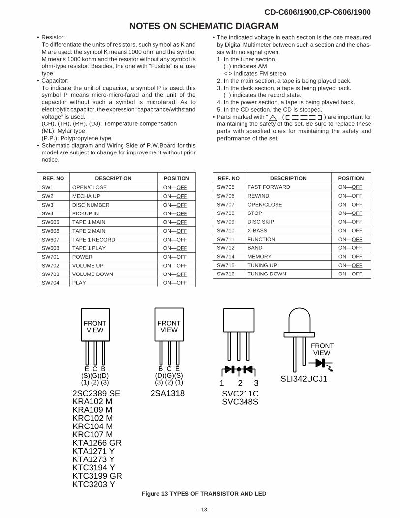
SW1 OPEN/CLOSE ON—OFF
SW2 MECHA UP ON—OFF
SW3 DISC NUMBER ON—OFF
SW4 PICKUP IN ON—OFF
SW605 TAPE 1 MAIN ON—OFF
SW606 TAPE 2 MAIN ON—OFF
SW607 TAPE 1 RECORD ON—OFF
SW608 TAPE 1 PLAY ON—OFF
SW701 POWER ON—OFF
SW702 VOLUME UP ON—OFF
SW703 VOLUME DOWN ON—OFF
SW704 PLAY ON—OFF
• The indicated voltage in each section is the one measuredby Digital Multimeter between such a section and the chas-sis with no signal given.1. In the tuner section,
( ) indicates AM< > indicates FM stereo
2. In the main section, a tape is being played back.3. In the deck section, a tape is being played back.
( ) indicates the record state.4. In the power section, a tape is being played back.5. In the CD section, the CD is stopped.
• Parts marked with “ ” ( ) are important formaintaining the safety of the set. Be sure to replace theseparts with specified ones for maintaining the safety andperformance of the set.
NOTES ON SCHEMATIC DIAGRAM• Resistor:
To differentiate the units of resistors, such symbol as K andM are used: the symbol K means 1000 ohm and the symbolM means 1000 kohm and the resistor without any symbol isohm-type resistor. Besides, the one with “Fusible” is a fusetype.
• Capacitor:To indicate the unit of capacitor, a symbol P is used: thissymbol P means micro-micro-farad and the unit of thecapacitor without such a symbol is microfarad. As toelectrolytic capacitor, the expression “capacitance/withstandvoltage” is used.(CH), (TH), (RH), (UJ): Temperature compensation(ML): Mylar type(P.P.): Polypropylene type
• Schematic diagram and Wiring Side of P.W.Board for thismodel are subject to change for improvement without priornotice.
REF. NO DESCRIPTION POSITION POSITION
SW705 FAST FORWARD ON—OFF
SW706 REWIND ON—OFF
SW707 OPEN/CLOSE ON—OFF
SW708 STOP ON—OFF
SW709 DISC SKIP ON—OFF
SW710 X-BASS ON—OFF
SW711 FUNCTION ON—OFF
SW712 BAND ON—OFF
SW714 MEMORY ON—OFF
SW715 TUNING UP ON—OFF
SW716 TUNING DOWN ON—OFF
REF. NO DESCRIPTION
Figure 13 TYPES OF TRANSISTOR AND LED
SVC211CSVC348S
2SC2389 SEKRA102 MKRA109 MKRC102 MKRC104 MKRC107 MKTA1266 GRKTA1271 YKTA1273 YKTC3194 YKTC3199 GRKTC3203 Y
FRONTVIEW
E C B(S)(G)(D)(1) (2) (3)
2SA1318
FRONTVIEW
B C E(D)(G)(S)(3) (2) (1) 1 2 3 SLI342UCJ1
VIEWFRONT

CD-C606/1900,CP-C606/1900
– 13 –
SW1 OPEN/CLOSE ON—OFF
SW2 MECHA UP ON—OFF
SW3 DISC NUMBER ON—OFF
SW4 PICKUP IN ON—OFF
SW605 TAPE 1 MAIN ON—OFF
SW606 TAPE 2 MAIN ON—OFF
SW607 TAPE 1 RECORD ON—OFF
SW608 TAPE 1 PLAY ON—OFF
SW701 POWER ON—OFF
SW702 VOLUME UP ON—OFF
SW703 VOLUME DOWN ON—OFF
SW704 PLAY ON—OFF
• The indicated voltage in each section is the one measuredby Digital Multimeter between such a section and the chas-sis with no signal given.1. In the tuner section,
( ) indicates AM< > indicates FM stereo
2. In the main section, a tape is being played back.3. In the deck section, a tape is being played back.
( ) indicates the record state.4. In the power section, a tape is being played back.5. In the CD section, the CD is stopped.
• Parts marked with “ ” ( ) are important formaintaining the safety of the set. Be sure to replace theseparts with specified ones for maintaining the safety andperformance of the set.
NOTES ON SCHEMATIC DIAGRAM• Resistor:
To differentiate the units of resistors, such symbol as K andM are used: the symbol K means 1000 ohm and the symbolM means 1000 kohm and the resistor without any symbol isohm-type resistor. Besides, the one with “Fusible” is a fusetype.
• Capacitor:To indicate the unit of capacitor, a symbol P is used: thissymbol P means micro-micro-farad and the unit of thecapacitor without such a symbol is microfarad. As toelectrolytic capacitor, the expression “capacitance/withstandvoltage” is used.(CH), (TH), (RH), (UJ): Temperature compensation(ML): Mylar type(P.P.): Polypropylene type
• Schematic diagram and Wiring Side of P.W.Board for thismodel are subject to change for improvement without priornotice.
REF. NO DESCRIPTION POSITION POSITION
SW705 FAST FORWARD ON—OFF
SW706 REWIND ON—OFF
SW707 OPEN/CLOSE ON—OFF
SW708 STOP ON—OFF
SW709 DISC SKIP ON—OFF
SW710 X-BASS ON—OFF
SW711 FUNCTION ON—OFF
SW712 BAND ON—OFF
SW714 MEMORY ON—OFF
SW715 TUNING UP ON—OFF
SW716 TUNING DOWN ON—OFF
REF. NO DESCRIPTION
Figure 13 TYPES OF TRANSISTOR AND LED
SVC211CSVC348S
2SC2389 SEKRA102 MKRA109 MKRC102 MKRC104 MKRC107 MKTA1266 GRKTA1271 YKTA1273 YKTC3194 YKTC3199 GRKTC3203 Y
FRONTVIEW
E C B(S)(G)(D)(1) (2) (3)
2SA1318
FRONTVIEW
B C E(D)(G)(S)(3) (2) (1) 1 2 3 SLI342UCJ1
VIEWFRONT
CD-C606/1900,CP-C606/1900
– 14 –
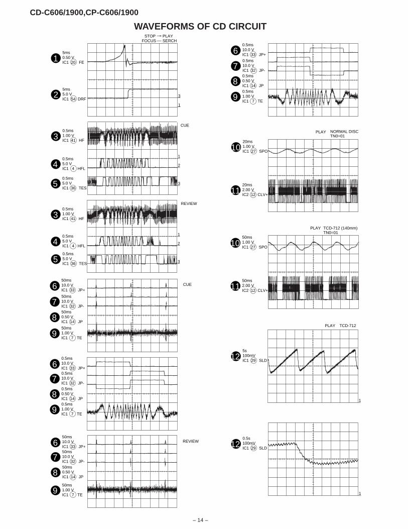
WAVEFORMS OF CD CIRCUIT
1
2
3
REVIEW0.5ms1.00 VIC1 41 HF
0.5ms5.0 VIC1 4 HFL
13
140.5ms5.0 VIC1 36 TES15
CUE50ms10.0 VIC1 33 JP+
50ms10.0 VIC1 32 JP-
16
1750ms0.50 VIC1 14 JP1850ms1.00 VIC1 7 TE19
0.5ms10.0 VIC1 33 JP+0.5ms10.0 VIC1 32 JP-
16
170.5ms0.50 VIC1 14 JP180.5ms1.00 VIC1 7 TE19
REVIEW50ms10.0 VIC1 33 JP+50ms10.0 VIC1 32 JP-
16
1750ms0.50 VIC1 14 JP1850ms1.00 VIC1 7 TE19
0.5ms10.0 VIC1 33 JP+
0.5ms10.0 VIC1 32 JP-
16
170.5ms0.50 VIC1 14 JP180.5ms1.00 VIC1 7 TE19
PLAY NORMAL DISCTN0=01
20ms1.00 VIC1 27 SPO
20ms2.00 VIC2 12 CLV+
110
111
PLAY TCD-712 (140mm)TN0=01
50ms1.00 VIC1 27 SPO
50ms2.00 VIC2 12 CLV+
110
111
PLAY TCD-712
1
5s100mVIC1 29 SLD112
1
0.5s100mVIC1 29 SLD112
3
5ms0.50 VIC1 20 FE
1
5ms5.0 VIC1 54 DRF
STOP PLAYFOCUS SERCH
11
12
1
2
3
CUE0.5ms1.00 VIC1 41 HF
0.5ms5.0 VIC1 4 HFL
13
140.5ms5.0 VIC1 36 TES15
CD-C606/1900,CP-C606/1900
– 15 –
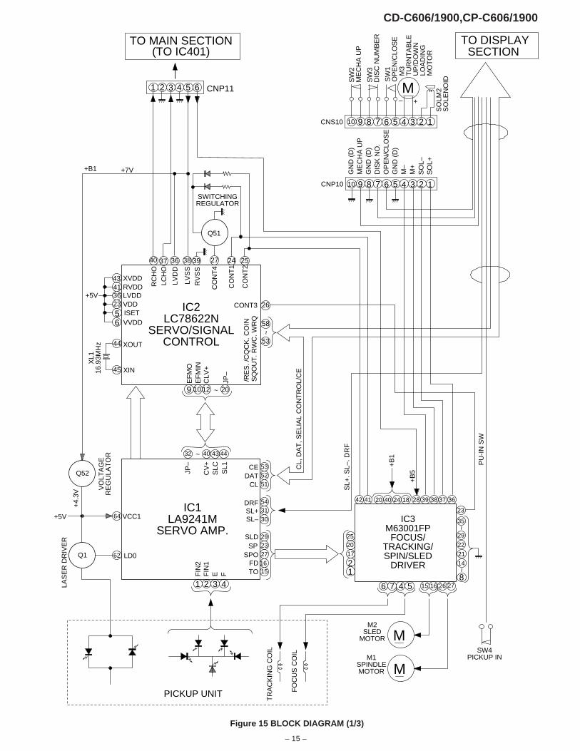
Figure 15 BLOCK DIAGRAM (1/3)
27
1 2 3 4
1
6 7
18244020
4 5 15
23
16 26 27
2
2520
3839284142 37 36
PU
-IN
SW
XL1
16.9
3MH
z
XIN
LD0
FIN
2
JP–
CV
+S
LC SL1
FIN
1E F TO
FDSPO
SPSLD
SL–SL+DRF
CLDAT
CE
VCC1
5
+5V
SW4PICKUP IN
FO
CU
S C
OIL
TR
AC
KIN
G C
OIL
M1SPINDLEMOTOR M
MM2
SLEDMOTOR
PICKUP UNIT
9
IC2LC78622N
SERVO/SIGNALCONTROL
+B
1
IC3M63001FPFOCUS/
TRACKING/SPIN/SLED
DRIVER
IC1LA9241M
SERVO AMP.
/RE
S. /
CQ
CK
. CO
INS
QO
UT
. RW
C. W
RQ
~
~
~C
L, D
AT
, SE
LIA
L C
ON
TR
OL/
CE
Q51
SL+
. SL–
. DR
F
9 8 7 6 5 4 3 2 1
GN
D (
D)
ME
CH
A U
PG
ND
(D
)D
ISK
NO
.O
PE
N/C
LOS
EG
ND
(D
)M
–M
+
9 8 7 6 5 4 3 2 1
CNP10
M
+5V
+B1
62
64
45
3623
43
37 36 3840 24 25
10
1 2 3 4 5 6
10
26
58
53
10 12 20
32 40 43 44
535251
543130
292327
1615
41
44
Q1
Q52
+4.
3V
+7V
VO
LTA
GE
RE
GU
LAT
OR
TO MAIN SECTION(TO IC401)
XOUT
EF
MO
EF
MIN
CLV
+
JP–
CO
NT
2
CO
NT
1
LCH
O
LVD
D
LVS
S
RC
HO
ISETVDDLVDDRVDDXVDD
SW
1O
PE
N/C
LOS
E
SW
2M
EC
HA
UP
SW
3D
ISC
NU
MB
ER
M3
TU
RN
TA
BLE
UP
/DO
WN
LOA
DIN
GM
OT
OR
SO
LM2
SO
LEN
OID
TO DISPLAYSECTION
CNS10
+B
5
CNP11
RV
SS
39
CO
NT
4
SWITCHINGREGULATOR
LAS
ER
DR
IVE
R
6 VVDD
CONT3
17
– +S
OL–
SO
L+
8
29
35
14
~~
21
22
CD-C606/1900,CP-C606/1900
– 16 –
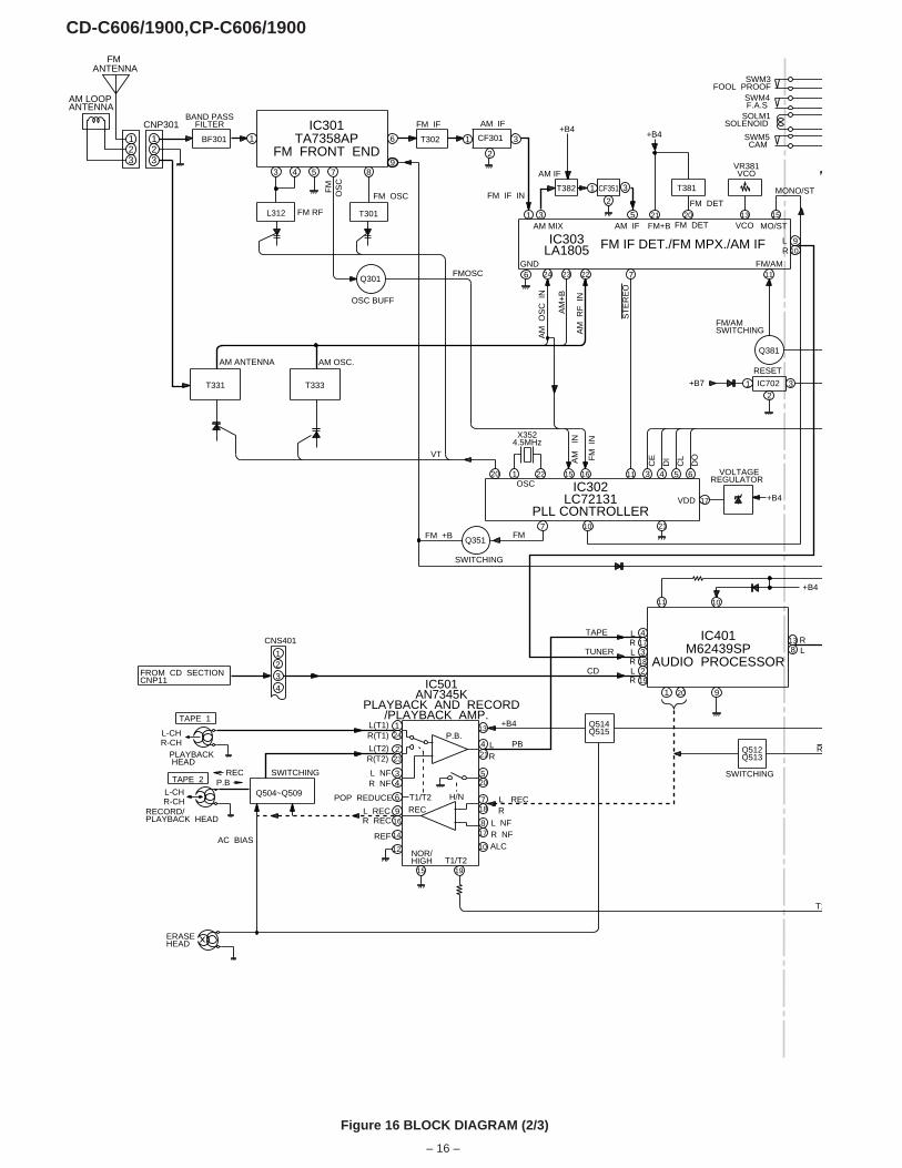
Figure 16 BLOCK DIAGRAM (2/3)
321
CNP301
321
FM ANTENNA
ANTENNAAM LOOP
1
2
3
6
5
2
1 3
21
22
1320
16
21
1 3
24 23
1520 1 22
15
9 10
117
11 3 4 5 6
10
GND
AM IF FM DET
FM DET
FM
IN
IC302LC72131
PLL CONTROLLER
OSC
VR381VCOAM IF
AM MIX
AM
IN
AM
+B
AM
RF
IN
X3524.5MHz
FMOSC
AM ANTENNA AM OSC.
T382
+B4 +B4
T381
IC303LA1805
L R
ST
ER
EO
AM
OS
C I
N
Q381
VT
DO
DI
CL
CE
1 24
2 23
3 4
4 21
5 20
6 7
178
9 16
10
14
12
13
18
H/N T1/T2
R-CHL-CH
L-CHR-CH
P.B REC
TAPE 2
TAPE 1
L NF
L(T1) R(T1)
L(T2) R(T2)
R NF
L R
POP REDUCE
L REC R REC
L R
REC
P.B.
REC
ALC NOR/HIGH T1/T2
REF
L NFR NF
PLAYBACK HEAD
RECORD/PLAYBACK HEAD
SWITCHING
Q504~Q509
AC BIAS
IC501AN7345K
PLAYBACK AND RECORD/PLAYBACK AMP.
PB
ERASEHEAD
+B4
1
34
CNS401
FROM CD SECTIONCNP11
17 +B4
VOLTAGEREGULATOR
SWM3FOOL PROOF
SWM4F.A.S
SOLM1SOLENOID
SWM5CAM
4 173
182 19
1 20 9
IC401M62439SP
AUDIO PROCESSORL R
L RL RL R
TUNER
TAPE
CD
3 IC702 1 +B7
2
T1
R
SWITCHING
Q512Q513
+B4
FM/AMSWITCHING
138
9
1
3 4 5 7 8
6
Q301
FM IF IN
FM IF
FM RF
FM
OS
C
T302
FM OSC
BAND PASSFILTER IC301
TA7358APFM FRONT END
T301L312
OSC BUFF
BF301
7 FM
Q351FM +B
SWITCHING
CF301
FM+B MO/STVCO
FM/AM
15 19
11 10
MONO/ST
T331 T333
CF351
AM IF
FM IF DET./FM MPX./AM IF
RESET
Q514Q515
2
VDD
CD-C606/1900,CP-C606/1900
– 17 –
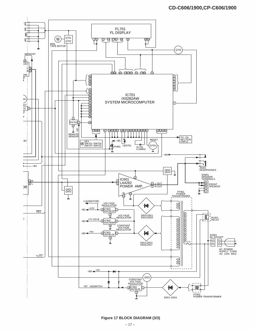
Figure 17 BLOCK DIAGRAM (3/3)
Q704
17
47
Q631Q632
3
IC903KIA7812P
2
1 3
IC902KIA7806P
2
1 3
IC901AN78L05
3
1 2
15
9 10
1
L R
81
+B4
3F
1 2 3 14 3021 31 32 33
9
IC701IX0282AW
SYSTEM MICROCOMPUTER
ORL R
XL7014.19MHz
+B5 KEY SW701~SW703SW707~SW722
+B5
M
TO CD SECTIONCNP12
MM1TAPE MOTOR
JK601HEADPHONES
SO601SPEAKERTERMINALS
T.F
PT901POWER
TRANSFORMER
RL901RELAY
AC POWERSUPPLY CORDAC 120V 60Hz
PT902POWER TRANSFORMER
IC904AN78L05
Q902
+B6
+B7 UNSWITCH
3 02
2
T1/T2
REC
G
+B4
D910,D911D914,D915
D912,D913D916,D917
2 3
1
+B
7
RX701
Q703
7 L-OUT
IC601LA4282POWER AMP.
+B
R-OUT
138
Q401Q402
+B1
+B4
+B5
+12V
+7V CD+B
+12V(MOTOR)
+5V
VOLTAGEREGULATOR
VOLTAGEREGULATOR
CONSTANTVOLTAGE
REGULATOR
CONSTANTVOLTAGE
REGULATOR
Q701Q702
O/ST
/AM
~ ~
25
12
17353413141516
29
193021222324252627
3938
52
4041
434244
49505154
7
654321
70 777360 807972 715856
MONO/ST
PHM1
D921~D924
FRONTSPEAKER
~ ~
3736
LED701
18 101112
10
11
SO901AC SOCKET
2
1 3
RESET
SET
REMOTESENSOR
57
FL701FL DISPLAY
+5V
CD-C606/1900,CP-C606/1900
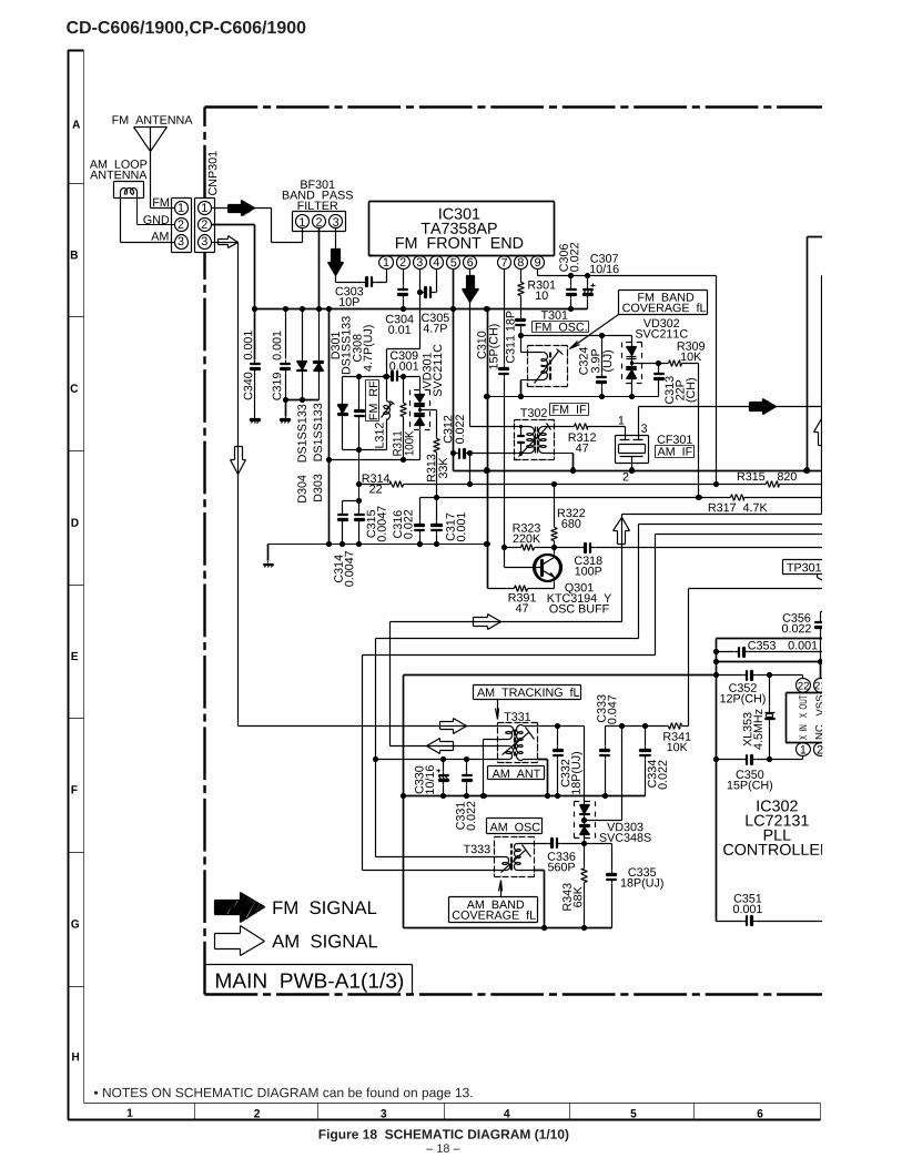
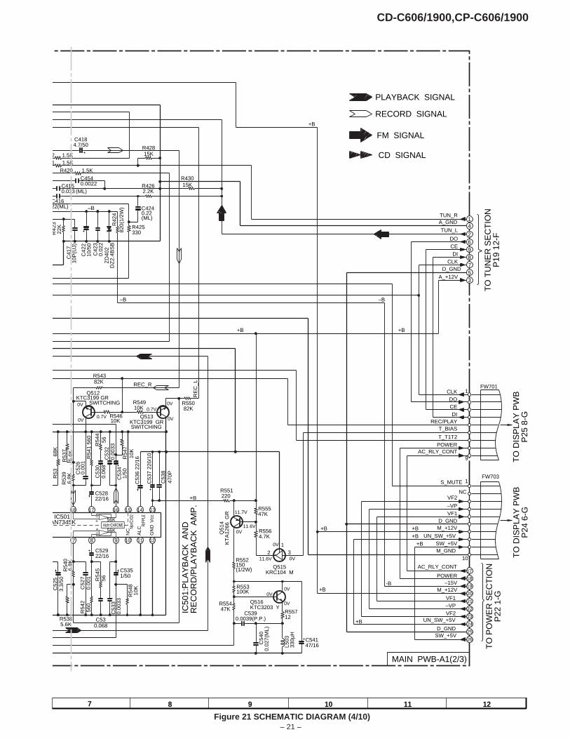
– 18 –Figure 18 SCHEMATIC DIAGRAM (1/10)
A
B
C
D
E
F
G
H
1 2 3 4 5 6
• NOTES ON SCHEMATIC DIAGRAM can be found on page 13.
FM BANDCOVERAGE fL
C3560.022
R39147
C35015P(CH)
C35212P(CH)
C3510.001
C353 0.001
XL3
534.
5MH
z
IC302LC72131
PLLCONTROLLER
Q301KTC3194 YOSC BUFF
L312
C30310P
R31
333
KR312
47
IC301TA7358AP
FM FRONT END
R315 820 R31422
R322680R323
220K
C318100P
R31
110
0K
C3090.001 C
311
18P
R30110
C3040.01
C3054.7P
C31
70.
001
C31
60.
022
C31
20.
022
C31
015
P(C
H)
C30710/16C
306
0.02
2
VD
301
SV
C21
1C
NC
X O
UTX
IN
VS
S
CN
P30
12 2
3 3
1 1 1 2 3
BF301BAND PASS
FILTER
C31
90.
001
D30
3D
S1S
S13
3D
304
DS
1SS
133
C34
00.
001
9 8 7 6 5 4 3 2 1
22 21
21 R34110K
C33
40.
022
C33
30.
047
C336560P
R34
368
K
C33518P(UJ)
C33
10.
022
C33
010
/16
T333
T331
C33
218
P(U
J)
AM OSC
AM ANT
FM ANTENNA
AM LOOPANTENNA
FM
GND AM
D30
1D
S1S
S13
3C
314
0.00
47C
308
4.7P
(UJ)
C31
50.
0047
T301
T302 FM IF
R317 4.7K
R30910K
C31
322
P(C
H)
VD302SVC211C
C32
43.
9P(U
J)
FM OSC.
CF301 AM IF
1
2
3
TP301
AM TRACKING fL
AM BANDCOVERAGE fL
MAIN PWB-A1(1/3)
AM SIGNAL
FM SIGNAL
VD303SVC348S
FM
RF
CD-C606/1900,CP-C606/1900
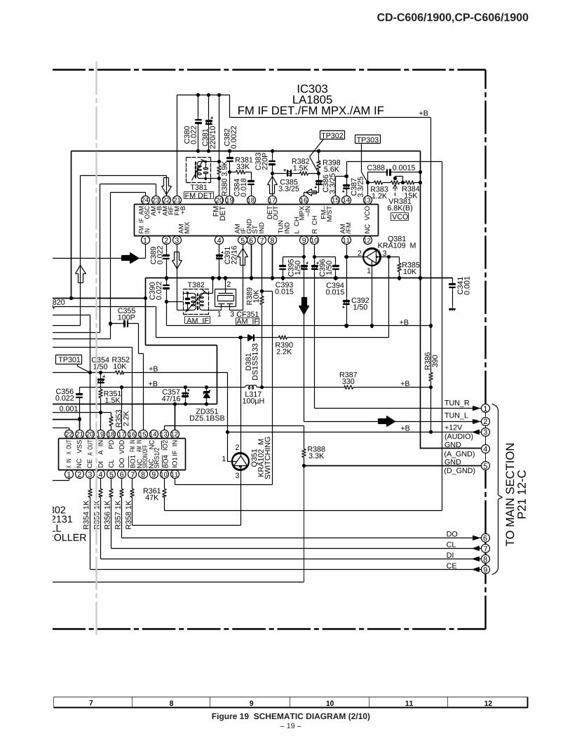
– 19 –Figure 19 SCHEMATIC DIAGRAM (2/10)
7 8 9 10 11 12
C3921/50
C3560.022
C34
10.
001
C38
322
0P
C3853.3/25
R3821.5K
R3985.6K
C38
63.
3/25
R3902.2K
D38
1D
S1S
S13
3
R3883.3K
C38
122
0/10
C38
00.
022
C38
20.
0022
Q35
1K
RA
102
MS
WIT
CH
ING
C35747/16
C355100P
0.001
R35
5 1K
R36147K
R35
4 1K
R35
6 1K
R35
7 1K
R35
8 1K
R35
32.
2K
3022131LL
ROLLER
ZD351DZ5.1BSB
L317100µH
R38
910
K
IC303LA1805
FM IF DET./FM MPX./AM IF
C3940.015
C39
122
/16
C38
90.
022
C388 0.0015R38133K
R38
0 3.
9K
C38
40.
018
R3831.2K
C39
00.
022
CF351
R38510K
Q381KRA109 M
C3930.015
C39
51/
50
C39
61/
50
R38415KC
387
3.3/
25
R387330
R38
639
0
R3511.5K
C3541/50
820
R35210K
NC
NC
+12V
CEDICLDO
GND
GND
TUN_L
TUN_R
(AUDIO)
(A_GND)
(D_GND)
X O
UTX
IN
VS
S
A O
UT
A I
N
IO1
DI
CE
AM
OS
CA
M +B
AM RF
AM
IFAM
MIX
AM
/FM
FM +B
FM
DE
T
DE
TO
UT
FM I
FIN G
ND
S
TIN
D
TU
N
IND
L
CH
R C
H VC
O
FM
–M
/ST
MP
X–I
N
TO
MA
IN S
EC
TIO
NP
21 1
2-C
24 23 22 21 20 19 18 17 16 15 14 13
12 11 109 8 7 6 5 4 3 2 1
22 21 20 19 18 17 16 15 14 13 12
11 10 9 8 7 6 5 4 3 2 1
T381FM DET
T382
AM IF 1
2
3 AM IF
TP302 TP303
+B
VR3816.8K(B)
VCO
1
2 3
+B
+B
+B
1
23
4
5
6789
1
2
3
IF I
N
+B
+B
TP301
NC
NC
NC
SR
S1/
2PD
VD
D
FM IN
AM IN
IO2
BO
4
BO
1
DO
CL
SRSO
N/OF
F
CD-C606/1900,CP-C606/1900
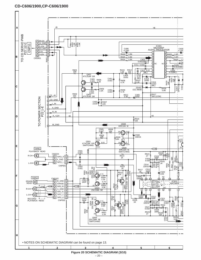
– 20 –
A
B
C
D
E
F
G
H
1 2 3 4 5 6
• NOTES ON SCHEMATIC DIAGRAM can be found on page 13.
Figure 20 SCHEMATIC DIAGRAM (3/10)
R45
11.
8K
R45
21.
8K
R4185.6K
C4530.0022(ML)
C55
20.
01C
551
0.01
C4510.001
C4520.001
R56
122
K
IC401M62439SP
AUDIO PROCESSOR
19
20
18
17
16
15
14
13
12
1110
9 8 7 6 5 4 3 2 1
IC501 AN7345K
C515220/10
C514220/10
R4084.7K
R5151K
C50
70.
001
Q50
7K
TC
3199
GR
R51247K
R51
34.
7K
R51
04.
7K
R50
110
K
R5385.6K
R54
256
0
C5230.022
C52
53.
3/50
C52
70
001
R50810K
Q508KRC104 M
Q509KRC104 MSWITCHING
QKTC3
R50
210
K
R54
06.
8KC5211/50
R52
74.
7K
C519180P
C5170.033
R53
75.
6K
R53
68K
R54
156
0
C52
60.
001
R53
96.
8K
R53333KR522
27 C518180P
R5311K
R5141K
C508100/16
R516150
ZD401DZ2.4BSB C
422
10/5
0
C4160.22(ML)
C4150.033 (ML)
R422 1.5KR421 1.5K
R42
322
K
R41
910
K
C41
710
P(U
J)
C4140.022(ML)
C41310/50
C4184.7/50
C412 0.22
C411 0.033
R416 1.5K
R415 1.5KR414 1.5K
C4064.7/50
C4100.22(ML)
R4132.2K
R4103.3K
C40410/50
R412330
Q401KTC3199 GR
C4010.001
R50910K
R5042.2K
R5053.3K
R5063.3K
R5072.2K
R50310K
C5050.047
Q501KTA1266 GRSWITCHING
Q5032SC2389 SE
Q50
22S
C23
89 S
ES
WIT
CH
ING
Q50
42S
C23
89 S
E
Q5052SC2389 SESWITCHING
C5010.001
C5020.001
C504180P
C503180P
CNP502
CNP501
R52327
C5160.033
R52
410
0KR
526
4.7K
C5201/50
C511330P
R5171K
C509330P
Q50
6K
TC
3199
GR
R51
147
K R532
1K
R52
510
0K
R53433K
R4052.2K
Q402KTC3199 GR
R4062.2KC402
0.001
R4094.7K
C40510/50
R4113.3K
R40722K
C40322/25
R417560 (1/2W)
R401330
R402330
NCNC
+12V+7V
CD_GND L-CH
A_GND R-CH
TAPE1_R
TAPE1_L A_GND
A_GND
M_GNDERASE
TAPE2_R2
TAPE2_R1TAPE2_L1
TAPE2_L2
9.3V
8.6V
9.3V
0V 3.4V
3.4V
0V
0V
0V
0V
0.7V
0V
0.7V0V
0V
0V
0.7V0V
0V
0V
0.7V
0V0V
0V
0V
0V
R-CH
L-CH
A_+12V
R_IN
L_IN
A_GND
CD_GND
CD_+B
M_GND
CNS101
ERASEHEAD
R-CH
L-CH
–
–+
+ 112K
112K
24 23 22 21 20 19 18
7 6 5 4 3 2 1
NC
NC
7 6
5 4 3
1
2
1
3 2
1
6
4 5
3 2
1
6
4 5
3
2
1
3
2
7
6 5 4
3
1 2
R420 1.5
C450.0
C50
60.
001
Hich=T1
CNS401
BI4
01
+B
(ML)
+B
+B
C512330P
C510330P
R5181K
132
1
23
TAPE1PLAYBACK HEAD
CNS102
RECORD/PLAYBACK HEAD
TAPE2
10
11
12
13
14
15
16
+B
TO
CD
SE
RV
O P
WB
P27
12-
C
CN
P11
TO
PO
WE
R S
EC
TIO
NP
22 1
-E
CD-C606/1900,CP-C606/1900
– 21 –Figure 21 SCHEMATIC DIAGRAM (4/10)
7 8 9 10 11 12
R42815K
R43015K
ZD
402
DZ
2.4B
SB
C53
847
0P
IC501 AN7345K
R55082K
R54382K
Q513KTC3199 GR
R54910K
R54
556
R5385.6K
R54
256
0
C5351/50
C52
53.
3/50
C52
70.
001
R54610K
Q512KTC3199 GR
C53
7 22
0/10R
547
10K
C530.068
C53
30.
0033
R54
810
K
R54
06.
8K
C53
6 22
/16 C
532
0.00
33
R53
75.
6K
C53
41/
50
R53
68K
R54
1 56
0
C52
60.
001
R53
96.
8K
C52822/16
C42
210
/50
C41622(ML)
C4150.033 (ML)
2 1.5K1 1.5K
R42
322
K
C41
710
P(U
J)
C4184.7/50
C42
30.
022
C54147/16 L5
0333
0µH
R55712
Q516KTC3203 Y
Q515KRC104 M
C54
00.
027(
ML)
R55547K
R5564.7K
C5390.0039(P.P.)
R553100K
R55447K
Q51
4K
TA
1266
GR
R552150 (1/2W)
R551220
C53
00.
068
R54
456
C52922/16
RE
C_L
REC_R
Vcc
GN
D
0V
0V0.7V
0.7V0V
0V
0V
11.7V
11.6V
11.6V
0V
0V
0V0V
0V
NC
A_GND
A_+12V
CLKDI
D_GND
CEDO
TUN_L
TUN_R
SW_+5V
AC_RLY_CONT
POWER
D_GND
UN_SW_+5V
–VP
M_+12V
VF2
VF1
–15V
NC
ALC
RIPP
LE
Nor/C
rO2
+
+
–
–56K
56K
18 17 16 15 14 13
1211109 8 7
R420 1.5K
C4540.0022 R426
2.2K
C4240.22(ML)
R425330
R42
482
0(1/
2W)
+B
–B
–B
+B
1 4
2 6 9 8 7 5 3
+B
–B
CLKDOCEDI
T_BIAS
T_T1T2POWER
AC_RLY_CONT
REC/PLAY
1
9
FW701
S_MUTE
VF2
–VPVF1
D_GNDM_+12V
UN_SW_+5V
FW703 1
10M_GND SW_+5V
+B+B
+B
+B
+B
+B
-B
17
18
19
20
21
22
23
24
25
26
TO
PO
WE
R S
EC
TIO
NP
22 1
-G
1 2 3
+B
SWITCHING
SWITCHING
Hich=CHROME
IC50
1:P
LAY
BA
CK
AN
DR
EC
OR
D/P
LAY
BA
CK
AM
P.
PLAYBACK SIGNAL
RECORD SIGNAL
FM SIGNAL
CD SIGNAL
TO
TU
NE
R S
EC
TIO
NP
19 1
2-F
TO
DIS
PLA
Y P
WB
P25
8-G
TO
DIS
PLA
Y P
WB
P24
6-G
MAIN PWB-A1(2/3)
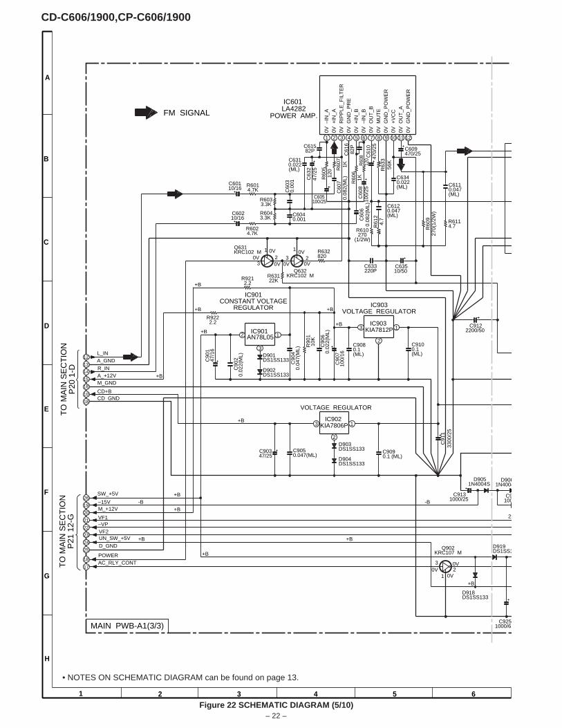
CD-C606/1900,CP-C606/1900
– 22 –Figure 22 SCHEMATIC DIAGRAM (5/10)
A
B
C
D
E
F
G
H
1 2 3 4 5 6
• NOTES ON SCHEMATIC DIAGRAM can be found on page 13.
C61
682
PR
606
1KR
608
120
C61582P
C6110.047 (ML)
R6114.7
C91
133
00/2
5
C6120.047(ML)
C60110/16
R632820
R63122K
Q632KRC102 M
Q631KRC102 M
C60210/16
R6024.7K
R6043.3K
R6033.3K
C6040.001
C60
30.
001
C63510/50
R61
24.
7
R610270
(1/2W)
R60
927
0(1/
2W)
C633220P
C6340.022 (ML)
C63
247
/25
C6310.022(ML)
IC601 LA4282
POWER AMP.
C61
047
0/25
C60
70.
082(
ML)
C60
810
0/25
C605100/25
R63
356
K
R60
71K
R60
512
0
C90
147
/16
C90
710
0/16
C9080.1(ML)
C9100.1(ML)
C90
60.
022(
ML)
R90
110
K
IC903 KIA7812P3 1
C90
20.
022(
ML)
D902DS1SS133
IC901 AN78L052 1
C90
40.
047(
ML)
D901DS1SS133
22
C9131000/25
D9051N4004S
D9061N4004
C9100
D903DS1SS133
D904DS1SS133
IC902 KIA7806P3 1
C90347/25
C9050.047(ML)
C9122200/50
1211109 8 7 6 5 4 3 2 1
2 3
2
C609470/25
D919DS1SS1
Q902KRC107 M
C9090.1 (ML)
12
13
14
15
16
10
18
26
19
20
22
21
24
23
25
18
17
CD+B
A_+12V
CD GND
A_GND
M_GND
0V G
ND
_PO
WE
R
0V +
VC
C0V
GN
D_P
OW
ER
0V
MU
TE
0V O
UT
_A
0V O
UT
_B
0V –
IN_B
0V
+IN
_B
0V G
ND
_PR
E
0V R
IPP
LE_F
ILT
ER
0V
+IN
_A
0V –
IN_A
R_IN
L_IN
SW_+5V
UN_SW_+5V
M_+12V–15V
VF1 –VP VF2
D_GND
POWER AC_RLY_CONT
1
2 3
1 2
3
IC901CONSTANT VOLTAGE
REGULATOR
+B
+B
+B
+B
+B
IC903VOLTAGE REGULATOR
3
1 2
+B
-B
+B
+B
+B
+B
+B
+B
-B
VOLTAGE REGULATOR
+B
TO
MA
IN S
EC
TIO
NP
20 1
-D
C9251000/6.
D918DS1SS133
MAIN PWB-A1(3/3)
FM SIGNAL
R6014.7K
TO
MA
IN S
EC
TIO
NP
21 1
2-G
C60
60.
082(
ML)
0V
0V 0V
0V 0V
0V
0V
0V
0V
R9212.2
R9222.2
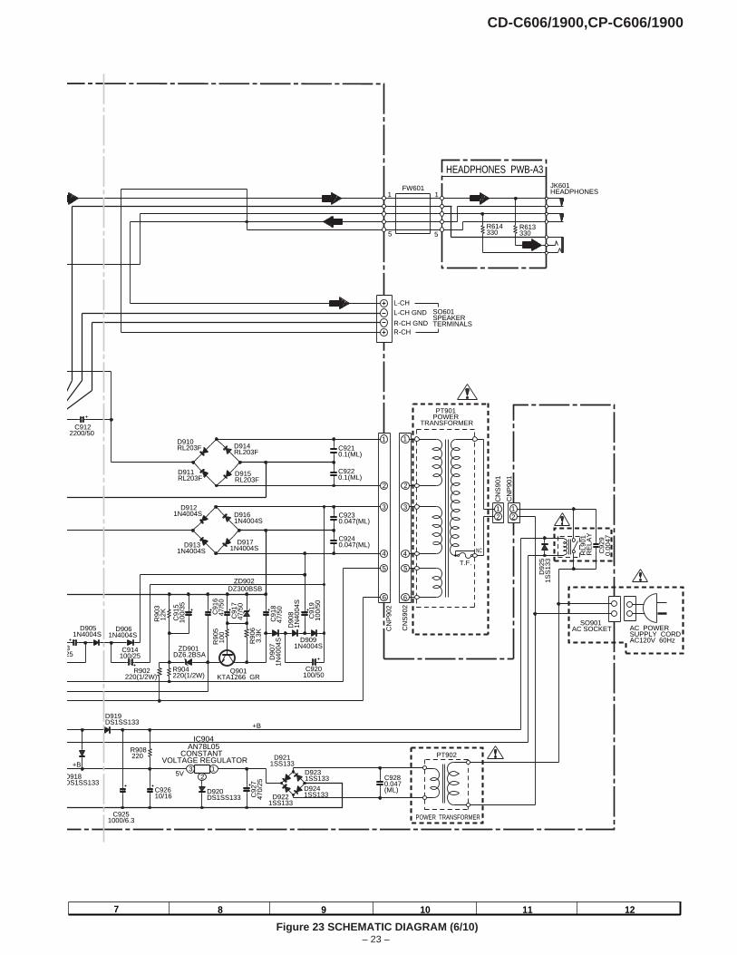
CD-C606/1900,CP-C606/1900
– 23 –Figure 23 SCHEMATIC DIAGRAM (6/10)
7 8 9 10 11 12
R902220(1/2W)
325
D9051N4004S
D9061N4004S
C914100/25 D
907
1N40
04S
D90
81N
4004
S
D9091N4004S
C91
910
0/50
C920100/50
Q901KTA1266 GR
R90
63.
3K
R90
510
0
ZD901 DZ6.2BSA
C91
847
/50
ZD902 DZ300BSB
C91
747
/50
C91
647
/50
R90
312
K
R904220(1/2W)
C91
510
0/35
C9230.047(ML)
D914RL203F
D9131N4004S
D910RL203F
C9220.1(ML)
D9121N4004S
D9171N4004S
D915RL203F
D9161N4004S
D911RL203F
C9240.047(ML)
C9210.1(ML)
C9122200/50
1
2
3
4
5
6
CN
P90
2
SO601SPEAKERTERMINALS
R613330
R614330
JK601 HEADPHONES
D919DS1SS133
1
5
1
5
L-CHL-CH GND
R-CH GNDR-CH
+B
+B
D92
51S
S13
3
RL9
01R
ELA
Y
CN
P90
1
PT901 POWER
TRANSFORMER
CN
S90
1
1
2
3
4
6
5
CN
S90
2
1 2
1 2
SO901 AC SOCKET
NC
T.F.
AC POWER SUPPLY CORD AC120V 60Hz
C92
90.
0047
C92
747
0/25
PT902
C9280.047 (ML)
D9211SS133
D9231SS133
D9241SS133D922
1SS133
D920DS1SS133
IC904 AN78L05
CONSTANT VOLTAGE REGULATOR
1 2
3
C92610/16
C9251000/6.3
D918DS1SS133
R908220
POWER TRANSFORMER
HEADPHONES PWB-A3
FW601
5V
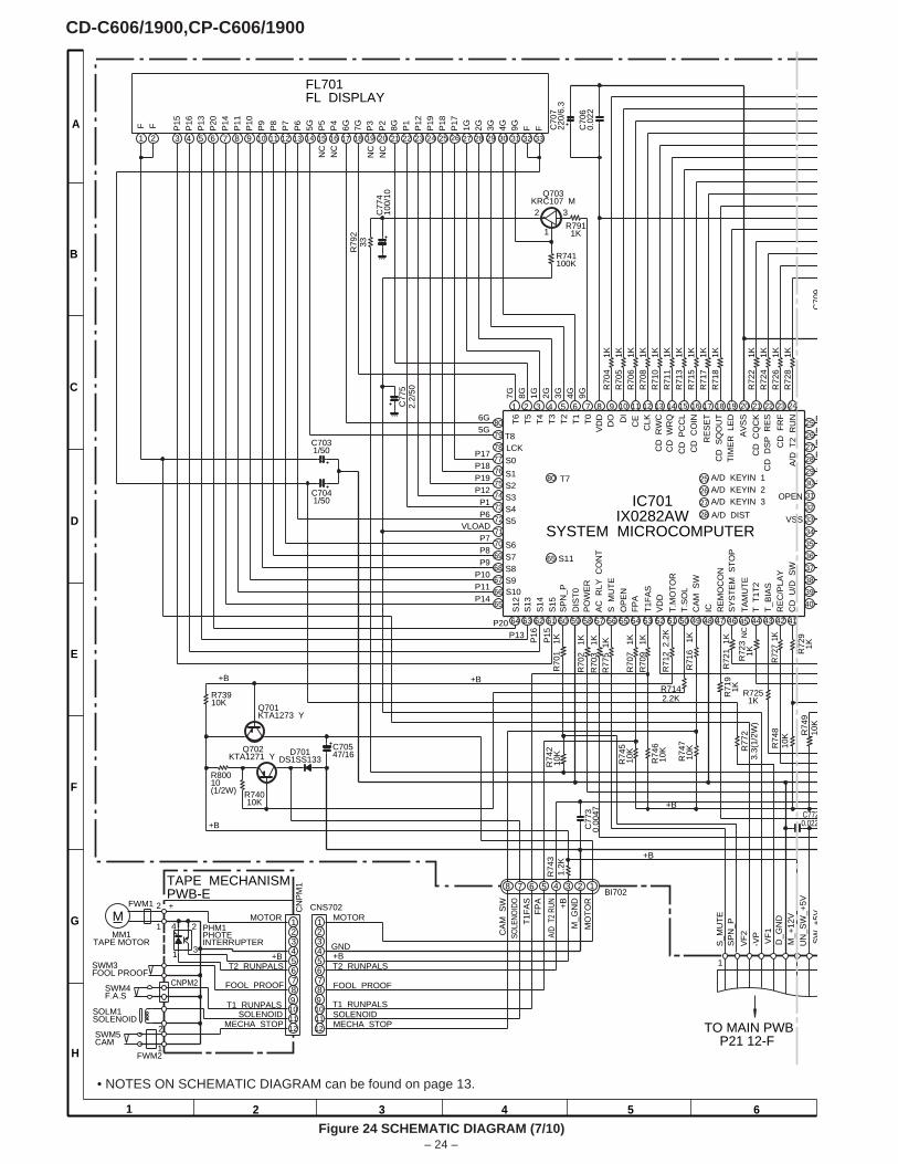
CD-C606/1900,CP-C606/1900
– 24 –Figure 24 SCHEMATIC DIAGRAM (7/10)
A
B
C
D
E
F
G
H
1 2 3 4 5 6
• NOTES ON SCHEMATIC DIAGRAM can be found on page 13.
R7911K
C77
52.
2/50
C77
410
0/10
R79
233
R77
5 1
K
R80010(1/2W)
C7031/50
R71
1
1K
R70
4
1K
R70
5
1K
R70
6
1K
FL701 FL DISPLAY
R71
3
1K
C70547/16
Q702KTA1271 Y
R74010K
R71
2 2
.2K
R7142.2K
R71
6 1
K
R70
9 1
K
R70
2 1
K
R72
6
1K
R72
8
1K
R70
7 1
K
R70
3 1
K
R73910K
Q701KTA1273 Y
C70
9
R72
91K
R72
1 1
K
R72
31K
R7251K
R72
71K
R71
91K
Q703KRC107 M
R70
8
1K
R72
2
1K
C7041/50
R741100K
R71
0
1K
R71
8
1K
R71
7
1K
R72
4
1K
R71
5
1K
IC701IX0282AW
SYSTEM MICROCOMPUTER
80
79
80
78
77
76
75
74
73
72
71
70
69
68
67
66
65
65
40
39
38
37
36
35
34
33
32
31
30
29
28
27
26
25
NC
NC
NC
NC
NC
S M
UT
E
VLOAD
CC
VD
D
VSS
AA
AV
SS
RE
SE
T
CD
CO
INC
D P
CC
LC
D W
RQ
CD
RW
CC
LK
VD
DT0
T1
T2
T3
T4
T5
T6
T7
T8
S0
S1S2S3S4S5
S6S7S8S9
S11
S12
S
13
S14
S
15
9G4G3G2G1G8G7G
6G5G
P17P18P19P12P1P6
P7P8P9
P10P11P14
P20 P13
P16
P15
F
F
P15
P
16
P13
P
20
P14
P
11
P10
P
9P
8P
7P
65G P
5P
46G 7G P
3P
28G P
1P
12
P19
P
18
P17
1G 2G 3G 4G 9G F
F
CD
SQ
OU
TT
IME
R L
ED
CD
CQ
CK
CD
DS
P R
ES
CD
FR
FA
/D T
2 R
UN
C
CD
U/D
SW
R
EC
/PLA
YT
_BIA
S
CE
T1F
AS
AC
RLY
CO
NT
DI
DO
T T
1T2
CA
M S
W
PO
WE
R
TA
MU
TE
T.M
OT
OR
T
.SO
L
RE
MO
CO
N
SY
ST
EM
ST
OP
FP
A
ICDIS
T0
3332313029282726252423222120191817161514131211109 8 7 6 5 4 3 2 1
64 63 62 61 60 59 58 57 56 55 54 53 52 51 50 49 48 47 46 45 44 43 42 41
24 23222120191817161514131211109 8 7 6 5 4 3 2 1
28
27
26
25 A/D KEYIN 1 A/D KEYIN 2 A/D KEYIN 3
A/D DIST
RRRR
R74
510
K
R74
610
K
R74
710
K
R74
910
K
R74
810
K
R77
23.
3(1/
2W)
C7720.022
R74
31.
2K
C70
60.
022
C70
722
0/6.
3
LCK
C77
30.
0047
8 7 6 5 4 3 2 1
MO
TO
R
1
2 3
S_M
UT
E
UN
_SW
_+5V
SW
+5V
M_+
12V
D_G
ND
V
F1
VF
2 -V
P
1
TO MAIN PWBP21 12-F
+B
+B
+B
SOLE
NOID
OC
AM
SW
T1F
AS
FP
A +B
M_G
ND
A/D
T2
RUN
BI702
+B
+B
1 2 3 4 5 6 7 8 9 1011
1 2 3 4 5 6 7 8 9 1011
1212
MOTOR
FOOL PROOF
T1 RUNPALS
MECHA STOPSOLENOID
T2 RUNPALS+BGND
CNS702CN
PM
1
PHM1
CNPM2
SWM3FOOL PROOF
4
3 1
+
MM1TAPE MOTOR
FWM1
M
FWM2
PHOTE INTERRUPTER
SWM5CAM
SWM4F.A.S
SOLM1 SOLENOID
TAPE MECHANISMPWB-E
1
2
2 MOTOR
+BT2 RUNPALS
FOOL PROOF
T1 RUNPALS
MECHA STOPSOLENOID
1
2
D701DS1SS133
S10
OP
EN
SP
N_P
OPEN
R70
1 1
KR
742
10K
SP
N_P
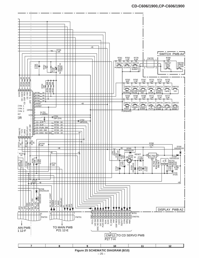
CD-C606/1900,CP-C606/1900
– 25 –Figure 25 SCHEMATIC DIAGRAM (8/10)
7 8 9 10 11 12
C77
00.
1/50
D743DS1SS133
R78
247
K
XL7014.19MHz
C70115P (CH)
R75
210
K
R72
6
1K
R72
8
1K
C70
90.
022
R72
91K
R72
31K
R7251K
R72
71K
1K
R7854.7K
C70218P(CH)
R72
2
1K
R730 1K
R72
4
1K
R734 1K
C71547/25
R786100
C71
40.
022
RX701 REMOTESENSOR
D704DS1SS133
IC70
2K
IA70
42P
RE
SE
T
3 1
D705DS1SS133
C71
30.
022
R78
310
0KD70
3D
S1S
S13
3
C7123.3/50
Q704KRC102 M
R731 1KR732 1K
R733 1K
ER
40
39
38
37
36
35
34
33
32
31
30
29
28
27
26
25
NC
CD O/C SW CD PUIN SW
CD SLM –
CD SLM +
VSS
AVREF AVDD
AV
SS
CD
CQ
CK
CD
DS
P R
ES
CD
FR
FA
/D T
2 R
UN
CD DISC NO SW
CD
U/D
SW
R
EC
/PLA
YT
_BIA
ST
T1T
2T
AM
UT
E
45 44 43 42 41
24 23222120
R7788.2K
R7621.2K
R761820
R7763.3K
R7732.2K
R7651.2K
R7671.5K
R763820
R7701.8K
R764820
R7773.3K
R7711.8K
R7661.2K
R7742.2K
R7681.5K
FW705
C71
00.
01D
702
DS
1SS
133
EYIN 1 EYIN 2 EYIN 3
IST
R735 1KR736 1KR737 1KR738 1K
R75
3 10
K
R75
4
10K
R75
610
K
R75
7
10K
R
755
3.3K
LED
701
SLI
342U
CJ1
TIM
ER
L701
100µ
H
C70
80.
001
R74
910
K
R75010K
R75110K R
748
10K
R77
23.
3(1/
2W)
C7720.022
9 8 7 6 5 4 3 2 1 101112131415
9 8 7 6 5 4 3 2 1 101112131415
PC
CL
U/D
SW
DIS
C N
O S
W
O/C
SW
PU
IN S
WS
LM–
SLM
+
D_G
ND
FR
FD
SP
RE
SC
QC
KS
QO
UT
WR
QC
OIN
RW
C
2
1 2 3
R7581.8K
+B
+B
SW707DISCSKIP
SW708OPEN/CLOSE
R7803.9K1
3
1
3
SW701 SW702 SW703
CLOCK POWER TIMER/ SLEEP
SW709 SW710 SW711 SW712 SW713 SW714 SW715
CDTUNER/BAND
MEMORY/SET STOP
RECORD/PAUSE
SW716 SW717 SW718 SW719 SW720 SW721 SW722
TUNINGUP
TUNINGDOWN PLAY
VOLUMEUPFAST
FORWARD
VOLUMEDOWN
+B
+B
+B
+B
+B
+B
1
2 3
BI701
CNS701
CNP12 TO CD SERVO PWB
AC
_RLY
_CO
NT
P
OW
ER
T
_T1T
2T
_BIA
S
RE
C/P
LAY
DI
CE
DO
CLK
1 9
FW701
D708DS1SS133
D70
7D
S1S
S13
3M
_GN
D
UN
_SW
_+5V
SW
_+5V
M_+
12V
D_G
ND
V
F1
VF
2 -V
P
FW703
TO MAIN PWBP21 12-E
AIN PWB1 12-F
+B
SWITCH PWB-A4
DISPLAY PWB-A2
TAPEREWIND
X-BASS/DEMO
10
IC702
P27 7-H
RESET
OPEN
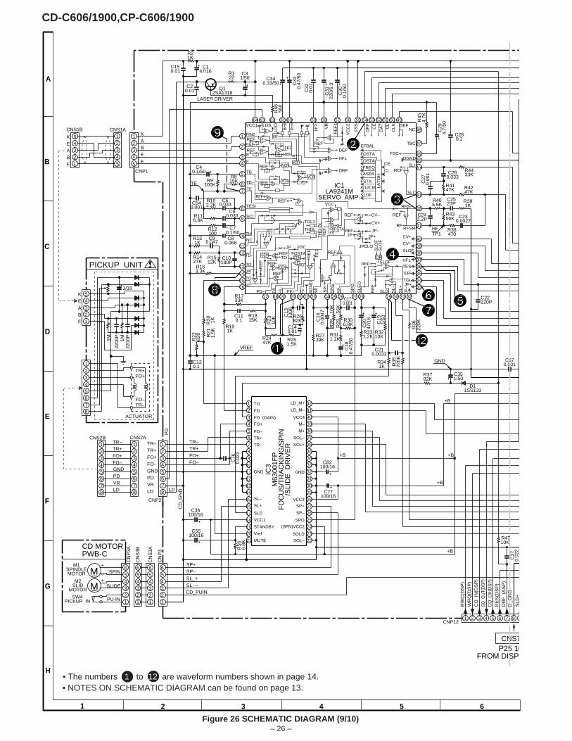
CD-C606/1900,CP-C606/1900
– 26 –
A
B
C
D
E
F
G
H
1 2 3 4 5 6
• NOTES ON SCHEMATIC DIAGRAM can be found on page 13.
Figure 26 SCHEMATIC DIAGRAM (9/10)
• The numbers 1 to 12 are waveform numbers shown in page 14.
D11SS133
C76
0.02
2
C77100/16
C570.001
R122
C20
47/1
6
C82100/16
C55100/16
R56
6.8K
C36100/16
IC3
M63
001F
PF
OC
US
/TR
AC
KIN
G/S
PIN
/SLI
DE
DR
IVE
R
C37
0.
022
R4710K
C2527P R39
1K
C15 0.01
R41 47K
R43 56K
R4433K
R4247K
C170.001
R306.8K
C31/50
R116.8K
C60.033
R102.2K
C50.033C54
0.001
R9100K
C16
0.00
47
R2739KR25
1.5K
R23
10K
R2447K
R1733K
C29
4.7/
50
C280.1
C140.01
C40.1/50
C351/50
Q12SA1318
R1815K
C110.1
IC1LA9241M
SERVO AMP.
4 8
4 7
6 4
4 5
4 4
43
42
41
40
39
38
37
36
35
34
33 16
15
14
13
12
11
10
9
8
7 6
5
4 3
2
1
C13
330P
R2682K
R3782K
C19
1/50
R331.2K
R32 10K
C32
0.01
C31
220/
6.3
C30
0.1/
50
C27
0.00
1
C242.2P
R405.6K
C260.033
R31 1.2K
C18
0.47
/50
R163.3K
R1512K
C10180P
C80.068
C70.1/50
R12100C9
0.047R131K
R1427K
C12 0.1
R21K
C147/16
C20.01
R46
560
R38470
C230.0027
R45
4.7K
C22 220P
C340.33/50 C
330.
47/5
0
NC
(SPN)VCC2
VCC4
LDVRPD
FO–FO+
TR+TR–
ACTUATOR
FO+
FO–TR–
TR+
1M
2200
P
1M22
00P
K
F B
E A
F B A E K
LD_M+
LD_M–
VCC3
M–
M+
SOL+
SOL–
SP–
SP+
SPO
SOL–
SOLD
MUTE
Vref
STANDBY
VCC1
SLD
SL–
SL+
GNDGND
TR+
TR–
FO–
FO+
FO (GAIN)
FD
TO
GND
LDVRPDGND FO–FO+ TR+ TR–
TP1 HF
TE
TBC
JPCLO
SLOF
SLO
FS
LOF
FSC
FE
1
FOSTA
FSC
EFBAL
RE
F
JPREF
CV–REF
CV+
JP–JP+
VREF
2FREQ LASER
8/12CM
FSTA
S.Q
.R
FOSTA
TOSTA
LAT
OH
FSTA
SLOF
CL
CE
DRF
HFL
DEF
VCC
TH
DG
L
THDL
TGL1
VCRVCR
VCRVCR
FE1
REF
–+
–+–+
–+
REF
RF
REF
DGND
SLI
FIN2
FIN1
F
E
TB
TE–
TE
TESI
SCI
REF
REF
REF
REF
REFREF
RE
F
REF
REF
REF TO
REF
REF
JP
RE
F
TH
TD
TD–
JP
TO
FD
GEN
GEN
GEN
FD– FA–
FA FE FE–
AG
ND
SP SP
I
SP
G
SP
–
SP
O
SLE
O
SLD SL–
SL+
RE
F
REF
RE
F
REF
OR
REF
RF
SLC
RFSM
JP–
JP+ TGL
TOFF
TESHFL
SLOF
CV–
CV+
64 63 62 61 60 59 58 57 56 55 54 53 52 51 50 49
32 3130292827262524 23222120191817
1
1
2
2 3 3
4
4 5
5
CNP1
1 2 3 4 5
1 2 3 4 5 6 7 8
1 2 3 4 5 6 7 8
1 2 3 4 5 6 7 8
7 8
CNP2
18
17
16
15
14
13
12
11
10
9 8 7 6 5 4 3
2 1
21
20
19
34
33
32
31
30
29
28
27
26
25
24
23
22
36
35
37
38
39
40
41
42
98 7 6 5 4 3 2 1 CNP12
1 2 3 4 5 6
CN
P3
1 2 3 4 5 6
1 2 3 4 5 6
1 2 3 4 5
CNS1A CNS1B
B
K A
F E
LASER DRIVER
+B
+B
+B
+B
+B
P25 10FROM DISPL
CNS7
RW
C(D
SP
)
D_G
ND
RE
S(D
SP
)
WR
Q(D
SP
)
DR
F (
AS
P)
SLD
+
CQ
CK
(DS
P)
CO
IN
(DS
P)
SQ O
UT(
DSP
)
1 2 3 4 5 6
SW4PICKUP IN
SPIN
SLIDE
PU-IN
+
–
–
+
1 2 3 4 5 6
CN
S3B
CN
S3A
M M1
SPINDLEMOTOR
M M2
SLIDMOTOR
CNS2A CNS2B
1/16
R815K
RFS–
R36
220K
R35
220KR341K
C210.0033
R20 1K
R191K
R21
1.5K
R22
820
FO–FO+ TR+ TR–
PD
LD
CD
_GN
D
CD_PUIN SL_–SL_+SP–SP+
CD MOTORPWB-C
PICKUP UNIT
VCC1 LDS
LDO
BH
I
LF2
PH
I
VR
RE
F1
FS
S
VC
C2
DR
F
DEF
CLK
C
L
DA
T
CE
NC
–+
–+ –+
–+
–+
–+
–+
–+
– +
–+
–+
–+
–+–+
–+
–+
–+ –+
–+
–+
–+
–+
–+
–+
–+
–+
R28
1
0KR
29
56K
CN
P3A
GND
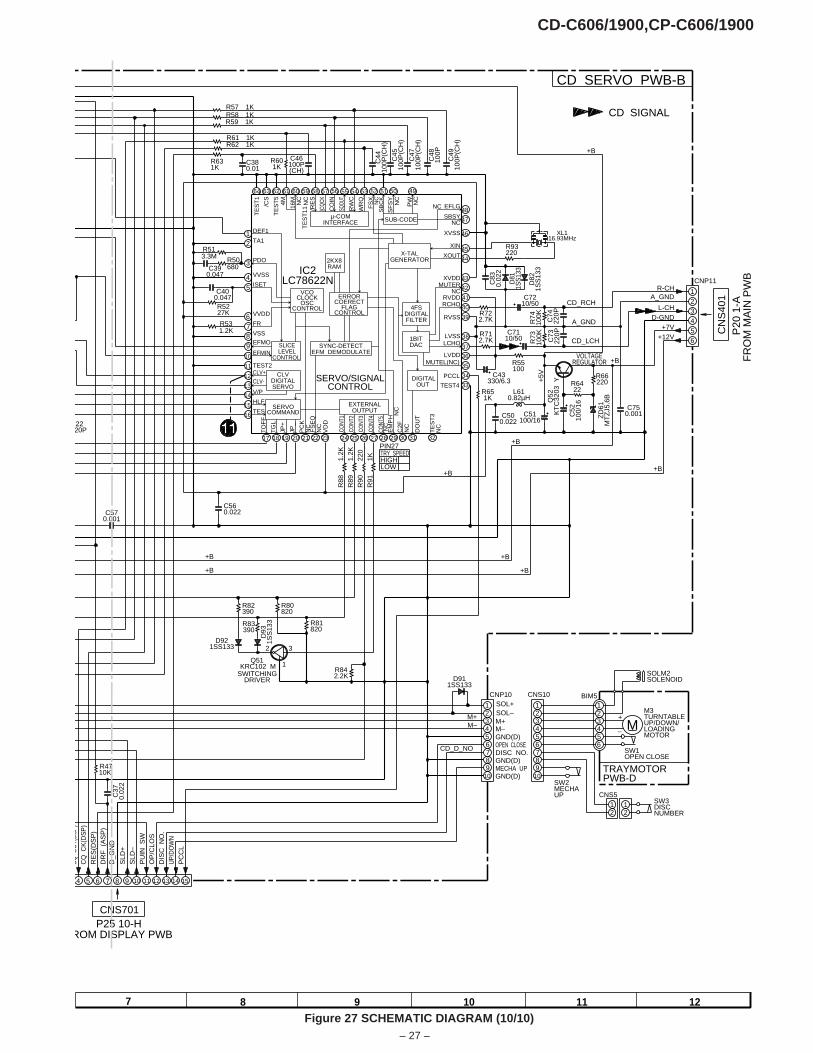
CD-C606/1900,CP-C606/1900
– 27 –
Figure 27 SCHEMATIC DIAGRAM (10/10)7 8 9 10 11 12
R842.2K
IC2LC78622N
R55100
C570.001
D82
1SS
133
C83
0.
022
R80 820
R81 820
Q51 KRC102 M
D921SS133
D93
1SS
133R83
390
R82 390
C56 0.022
R91
1K
D911SS133
Q52
KT
C32
03 Y
C52
100/
16
R6422
R66220
ZD
61M
TZ
J5.6
B
C51100/16
C500.022
L610.82µH
C37
0.
022
R4710K
C46100P(CH)
R513.3M
R88
1.2K
R93 220
D81
1SS
133
C45
100P
(CH
)
C44
100P
(CH
)
R89
1.2K
R90
220
R50 680 C39
0.047
C400.047R5227K
R601K
R57 1KR58 1K
R61 1K
R59 1K
C38 0.01
R631K
R62 1K
C49
100P
(CH
)
C48
100P
C43330/6.3
R74
100K
R73
100K
C73
220P
C74
220P
R531.2K
C22 20P
C47
100P
(CH
)
C750.001
C7210/50
R712.7K
R722.7K
NC
NC
CD_RCH
A_GND
XL116.93MHz
+5V
TE
ST
5
/CS
TA1
SOL+SOL–M+M–GND(D)OPEN CLOSEDISC NO.GND(D)MECHA UPGND(D)
2KX8RAM
1BITDAC
SERVOCOMMANDTES
HLF
V/P
CLV-
CLV+TEST2
EFMIN
EFMO
VSS
FR
VVDD
ISET
VVSS
PDO
DEF1
TO
FF
TG
L
JP+
JP_
PC
K
FS
EQ
VD
D
CO
NT1
CO
NT2
CO
NT3
CO
NT4
CO
NT5
EM
PH
C2F
CLVDIGITALSERVO
EXTERNALOUTPUT
SYNC-DETECTEFM DEMODULATE
SLICELEVEL
CONTROL
VCOCLOCK
OSCCONTROL
ERRORCOERECT
FLAGCONTROL
DIGITALOUT
TE
ST
3
DO
UT
4FSDIGITALFILTER
TE
ST
1
TEST4
MUTEL(NC)LVDD
LCHOLVSS
RVSS
RCHORVDD
XVDD
XOUT
XIN
XVSS
SUB-CODEµ-COMINTERFACE
TE
ST
11 SB
CK
SF
SY
PW
FS
X
WR
Q
RW
C
SQOU
T
CO
IN
/CQ
CK
/RE
S
16M4M
X-TALGENERATOR
64 63 61 62 60 59 58 57 56 55 54 53 52 51 50 49
32 31 30 29 28 27 26 25 24 23 22 21 20 19 18 17
3
2 1
48
47
45
44
43
42
41
40
39
38
37
36
35
34
33
16
15
14
13
12
11
10
9 8 7 6
5 4
46
2 3 4 5 6
1
7 8 9
10
2 3 4 5 6
1
7 8 9
10
2 3 4 5 6
1
CNP10
1 1 2 2
–
+
15 14 13 12 11 10 9 8 7 6 5 4
1 2 3 4 5 6
CNP11
+12V
D-GND+7V
L-CH
A_GNDR-CH
P20
1-A
FR
OM
MA
IN P
WB
CN
S40
1
C7110/50
VOLTAGEREGULATOR +B
+B
+B
+B
+B
PIN27
LOW HIGHTRY SPEED
SOLM2SOLENOID
M M3TURNTABLEUP/DOWN/LOADINGMOTOR
SW1OPEN CLOSE
SW2MECHAUP
SW3DISCNUMBER
CNS5
CNS10
1
2 3
SWITCHINGDRIVER
+B
+B
P25 10-HROM DISPLAY PWB
CNS701
PC
CL
OP
/CLO
S
UP/
DO
WN
D
ISC
NO
.
D_G
ND
RE
S(D
SP
)D
RF
(A
SP
)
SLD
+S
LD–
PU
IN S
W
CQ
CK
(DS
P)
SQ O
UT(
DSP
)
SERVO/SIGNALCONTROL
CD_LCH
R651K
CD_D_NO
M–M+
CD SERVO PWB-B
CD SIGNAL
TRAYMOTORPWB-D
NC
NC
NC
NC
SBSY
EFLGNC
NC
MUTERNC
NC
NC
NC
NC
NC
PCCL
+B
+B
BIM5
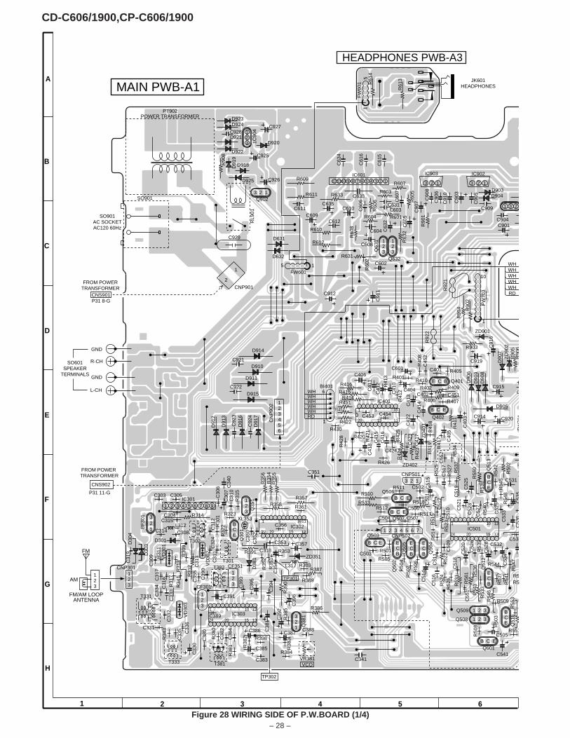
CD-C606/1900,CP-C606/1900
– 28 –Figure 28 WIRING SIDE OF P.W.BOARD (1/4)
A
B
C
D
E
F
G
H
1 2 3 4 5 6
C303
C331
R34
3
C33
5
C33
2
C33
4C
317
C31
6R
317
R34
1
C35
5
C39
0
C389
C33
6
C38
0
R38
0
C38
2
C38
4
R38
2 R398
C383
R38
1
R35
2R
351
R388
R389
R38
5R
383
R384
R52
4R
526
C51
8
C55
1
R53
6R
533
R53
7R
541
R509
R50
3
R50
8
R557
R55
3
R544
R54
7
R5R5
C538C532
R53
9
C52
6
C51
0C51
2R
514
C50
9
C51
1
R50
6
R50
7R
504
C52
3
C52
7R
540
C53
3R
545
R54
8
R54
2
R53
8
C51
9
R52
5
R52
7
C502
C506R517
C507
R512
R511
C504
R501C503
R505
R361
C356
C353
R353
C35
2C
350
R31
5C
310
C30
6
R323
R32
2R30
1C
312
C32
4C
311
C31
3R30
9R
313
R31
1
C30
9
C314 C308
C315C304
C305
C31
9
C453
R420
R430
R42
8
R42
1
C454
R41
2
R41
3
R42
5
R426
C42
3C
417
R407C451C402
R410
R41
8R
419
C55
2 R53
4
R40
8C
452
C401 R405R401
R60
2
R409
123
123
HEADPHONES PWB-A3
JK601HEADPHONES
C50
1
IC501
CNP502
IC302
IC401
FW
703
IC601
CNP301
C33
3
VD
303
T331
T333
C33
0
C391
CF351 T382
CF301
IC303
C386
C385
T381
C39
3
C39
5
C39
4C
381 C
392
C387
C39
6
R39
0
R387
R386
C388
VR381
Q38
1
C341
Q509
Q508
C505
Q501C541
Q51
6
R54
6R54
3R56
1
R53
1
Q51
2
C51
4
C51
6
C53
4
C53
5C
536
C52
9
C531
C52
0
R52
2
R51
5
R52
3
R518
Q506
Q507
Q50
2
Q50
5
Q50
4
C52
8
Q503
R510
R513R357
ZD351
L317
C318R391
C357
D38
1T301
Q30
1
XL353
R358
Q35
1IC301
R314
T302
L312
D301
VD
302
R31
2
VD
301
BF
301
D30
4
D30
3
D91
2
D91
3C
340
C30
7
R35
6R
354
R35
5
C92
3D
916
C92
4D
917
CN
P90
2
C351 CNP501
C41
5C
418
C424
C41
6
R42
4
ZD402
R42
3Z
D40
1
R41
7
C42
2
R422
C51
7
C51
5
R53
2C
521
R55
0
C52
5
R50
2
Q51
3
CR
C914
C40
5 FW
701
D905
D90
6
D90
9D
908
Q401
R406
R402
Q402
R41
1
C41
4
C
R90
6R
905
ZD
902
D90
7
C91
6
ZD901
R903
C919C601
C404C
410
C41
1
C41
2C406
R451R452
R416
R415R414
C40
3
C41
3
BI401 C915
C920
D914
D910
D911
D915C922
C921
SO901
C929
CNP901
FW601
D631
D632
R612
R610
C609C612
C635C611 C610
R60
8
R631
C912
C91
1
C602Q632
Q63
1
C608
R604
C604 C63
2
R601
R90
4 R90
2
R63
2C
605
R90
1
C904C901
FW
601 R
614
R61
3
IC902 IC903
D903D904
C909
C90
8
C90
6
C91
0
C90
3
C90
5
C90
7R60
5
R607
C60
7R603
C631C603C
606
C633
R60
6
R633
C63
4
C61
6
C61
5
1C90
4
C927
D920
C925
C926
Q902
R609
R611
D918
D925
D91
9
R90
8
D924D923
C928D921
D922
PT902 POWER TRANSFORMER
RL9
01
2
1
SO901AC SOCKETAC120 60Hz
FROM POWERTRANSFORMER
CNS901P31 8-G
GND
R-CH
GND
L-CH
SO601SPEAKER
TERMINALS
FROM POWER TRANSFORMER
CNS902
P31 11-G
TP302
VCO
C35
4
TP301
6
1
WHWHWHWHWHRD
WHWHWHWHWHRD
AM
FM/AM LOOPANTENNA
FM
R92
2
R92
1
123
3 2 1
123
123
121110 9 8 7 6 5 4 3 2 1 3 2 1 3 2 1
1 3 2
BCE
ECB
ECB
ECB
ECB
B C E
B C E
B C E
B C E
BCE
1 2 3
1 2 3
1 2 3 4 5 6 7
3 2 1
B C E
E C B
123456
123
BCE
1
32
321
123
15
1
10
15
1 5 10 12
15 132024
1 5 10
111520
1 5 1011
12152022
1 5 10 12
13152024
1 2 3 4 5 6 7 8 9
MAIN PWB-A1
123
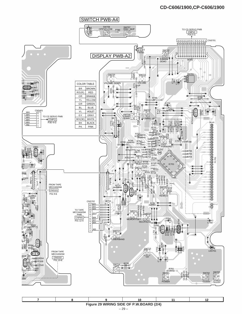
CD-C606/1900,CP-C606/1900
– 29 –Figure 29 WIRING SIDE OF P.W.BOARD (2/4)
7 8 9 10 11 12
IC701
R53
7R
541
R509
R557
R55
3
4
R54
7
R556R555
R76
3
C53832
C53
3R
545
R54
8 R51
6
R74
8R
740
R73
9
R77
5R
703
R70
2
R74
5
R70
7
R719
R723
R727R725
R721
R704R705R706
R730
R733R732R731
C702
C701
R753R754
R734
R72
4
R72
2
R708
C70
6
R751
R750
C77
2
R76
8
R76
6
R75
2
R755
R71
7
R71
3R
710
R79
1
R71
8
R71
5
R71
1
C71
4
R780
C708
321
SWITCH PWB-A4
DISPLAY PWB-A2
BL
BL
BL
BL
BL
BL
BL
BL
BL
BL
BL
BL
BL
BL
RD
R70
1R
742
C505
C541
Q51
6
R554
C539
C540
L503
Q514
R55
2
Q51
5
R776
SW715
D70
2 R78
2
C77
0
C71
0
R761
SW701 SW702 SW703
R76
2
R77
8
D70
4
D70
5
LED701
C703IC70
2
D70
3R
783Q
704
C71
3R
785
C712
L701
D743
SW710 SW711
R76
7R
765
C773
SW713
C53
4
R551
C53
0
R77
3
BI702
C53
7C53
5C
536
C52
9
R74
3C531
R50
2
C508R549
FW
701
D70
1R
800
R770
Q70
2
Q70
1
R71
6 R71
4R
712
R70
9
C70
5
R747
SW709
R74
6
FL7
01
C707
XL701
R728
R726
R738R737R736
R735R756R757
D708R749
SW719
R729
SW712
FW
701
SW716
D905
C91
8
C91
7
C913
Q901
R90
6R
905
ZD
902
D90
7
915
C920
C904C902
D902C901
FW
703
D70
7
R77
2
R76
4
SW717
R786
C709
Q70
3
R74
1
C77
5
C70
4
R792
C774
RX701
C71
5
SW722
BI701
FW705
R77
7
SW721
R77
4R
771
SW720
D901
IC901
0304
FW
705
R758
OPEN/CLOSESW707 DISC SKIP
SW708
VOLUME DOWN VOLUME UP
DOWNTUNING SW718
TUNING UP
PLAY
STOP
REWIND
REC/PAUSE MEMORY/SET
TUNER/BAND
CD
SW714 TAPE
POWER CLOCK TUMER /SLEEP
X-BASS/DEMO
FASTFORWARD
FROM TAPEMECHANISM
CNS101
P31 9-E
FROM TAPE MECHANISM
CNS102P31 10-E
121110987654321
WHGYWH
GYWH
GY
WH
RD
CNS702
TO TAPEMECHANISM
PWB
CNPM1
P31 12-A
8
1
15 1
15 14 13 12 11 10 9 8 7 6 5 4 3 2 1 CNS701
CNP12P30 5-G
TO CD SERVO PWB
654321
WHWHWHWHWHRD
CNS401
TO CD SERVO PWB
CNP11P30 4-G
BR
COLOR TABLE
RD(R)
OR
YL
GR
BL
VL
GY
WH(W)
BK
PK
BROWN
RED
ORANGE
YELLOW
GREEN
BLUE
VIOLET
GRAY
WHITE
BLACK
PINK
1 3 2
123
21
321
BCE
BCE
321
321
B C E
BCE
ECB
1
3
1 3
1
9
15
1015
20
25
30
3540
4550
55
60
65
70
7580
2
3
1
10
1
9
3332313029282726252423222120191817161514131211109876543
24
41
64
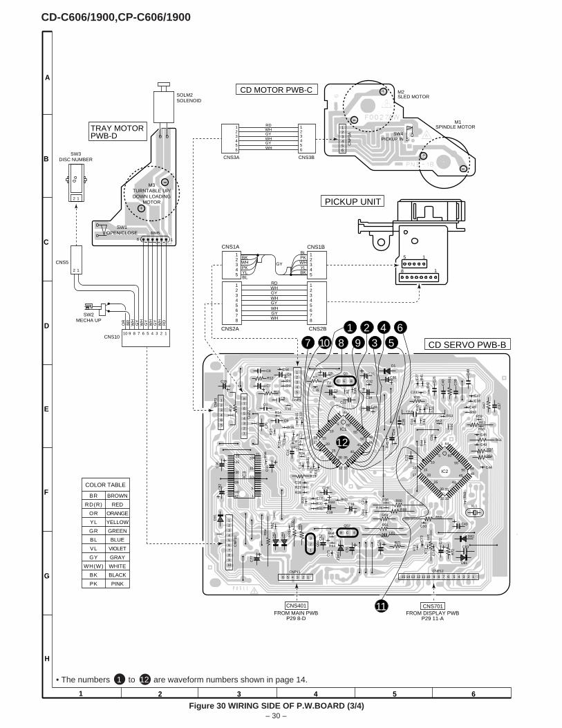
CD-C606/1900,CP-C606/1900
– 30 –
• The numbers 1 to 12 are waveform numbers shown in page 14.
Figure 30 WIRING SIDE OF P.W.BOARD (3/4)
A
B
C
D
E
F
G
H
1 2 3 4 5 6
-
123465
87654321
12345
C E B
B C E
3
2
1
1
2122
42
1
16
17
32 33
48
49
64
1
16
17
32 33
48
49
64
123456789
10
6 5 4 3 2 1 15 14 13 12 11 10 9 8 7 6 5 4 3 2 1
5
10
15
20
25
30 35
40
45
50
55
60
5
10
15
20
25
30 35
40
45
50
55
60
5
10
15
2025
30
35
40
IC2
IC1
R82
R83
R66
R64
C75
R33 R32
R29
C17
R30
R31
C16 R27
R28
C14
R25
R
26
C13
R56
IC3
R24
C21
R
34
R73
C73
R
74
C74
C50
R36
R35
R93
C44
R58
R59
C49
C45
C38
C47
R60
C46
C27
R
41
R42
C23
R40
C25
R38
C24
R43
R53
R52
R50
C56
R44
R45
C32
R46
R1
C2
C15
C54
R8R9
R10
R15
C
10
R16
R14
R13
R20
R21
R22
R17
R23
R18
SPINDLE MOTORM1
15
18
BR
COLOR TABLE
RD(R)
OR
YL
GR
BL
VL
GY
WH(W)
BK
PK
BROWN
RED
ORANGE
YELLOW
GREEN
BLUE
VIOLET
GRAY
WHITE
BLACK
PINK
CNS5
2 1
2 1
CNS10
WH
RD
GY
WH
BR
WH
GY
OR
WH
GY
10 9 8 7 6 5 4 3 2 1
SW2MECHA UP
SW1OPEN/CLOSE
CNS1BCNS1A
CNS2BCNS2A
CNS3BCNS3A
BLYLPKWHBK
GY
RDWHGYWHGYWHGYWH
RDWHGYWHGYWH
BLPKWHYLBK
12345678
12345678
123456
123456
12345
12345
PICKUP UNIT
CD MOTOR PWB-CSOLM2SOLENOID
CD SERVO PWB-B
CNS701FROM DISPLAY PWB
P29 11-A
CNS401FROM MAIN PWB
P29 8-D
PICKUP IN
CN
P3A SW4
SLED MOTORM2
M3TURNTABLE UP/DOWN LOADING
MOTOR
SW3DISC NUMBER
1
BIM5
6
TRAY MOTORPWB-D
+
-
+
-+
123456
CN
P10
D91
R84
C77
D93
D92
R80
Q51
R81
C52
CNP11
C51
ZD
61
R71
C71
L61
R91
R89
R88
R90 C19
C18
C20
R55
C72
R65
R72
CNP12
D81
C83
D82
C43
XL1
R61
R63
R62
R57
C22
C57
C28
C29
R47
C37
R19
C11
C33
C55
C36
C
82
CN
P3
R37
CN
P2
C76
C9
C6
C5
R11
C7
C8
R12 C4
C35
CNP1
C31
C34
C30
D1
Q1C3R2
C1
C12
R39
C26
C40
R51
C39
C48
Q52
11
53986421
10
12
7
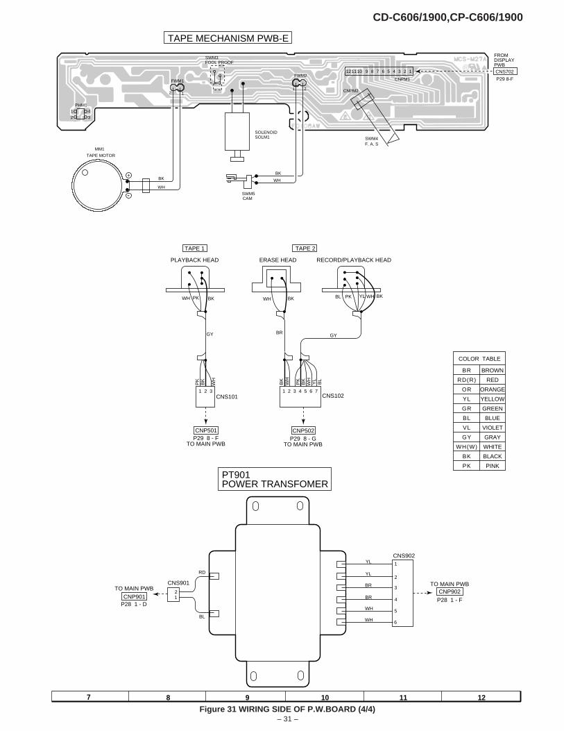
CD-C606/1900,CP-C606/1900
– 31 –Figure 31 WIRING SIDE OF P.W.BOARD (4/4)
7 8 9 10 11 12
WH PK BK
TAPE 1
PLAYBACK HEAD
TAPE 2
ERASE HEAD
RECORD/PLAYBACK HEAD
BL PK YL WH BKWH BK
GYBRGY
BL
CNS102CNS101
YL
WH
BK
PK
WH
BK
765432121 3
WH
BK
PK
CNP502P29 8 - G
TO MAIN PWBP29 8 - F
TO MAIN PWB
CNP501
P28 1 - D
TO MAIN PWBCNP901
CNS901
P28 1 - F
TO MAIN PWBCNP902
CNS902YL
RD
BL
PT901POWER TRANSFOMER
BR
COLOR TABLE
RD(R)
OR
YL
GR
BL
VL
GY
WH(W)
BK
PK
BROWN
RED
ORANGE
YELLOW
GREEN
BLUE
VIOLET
GRAY
WHITE
BLACK
PINK
2
1
12
3
4
5
6
YL
BR
BR
WH
WH
R
CNPM1
CNPM21 212
FWM1FWM2
SWM3
SWM4F. A. S
FOOL PROOF
123456789101112
34
21
PHM1
CNS702
FROMDISPLAYPWB
SOLM1
TAPE MOTOR
SOLENOID
MM1
+
- SWM5CAM
BK
WH
TAPE MECHANISM PWB-E
BK
WH
P29 8-F
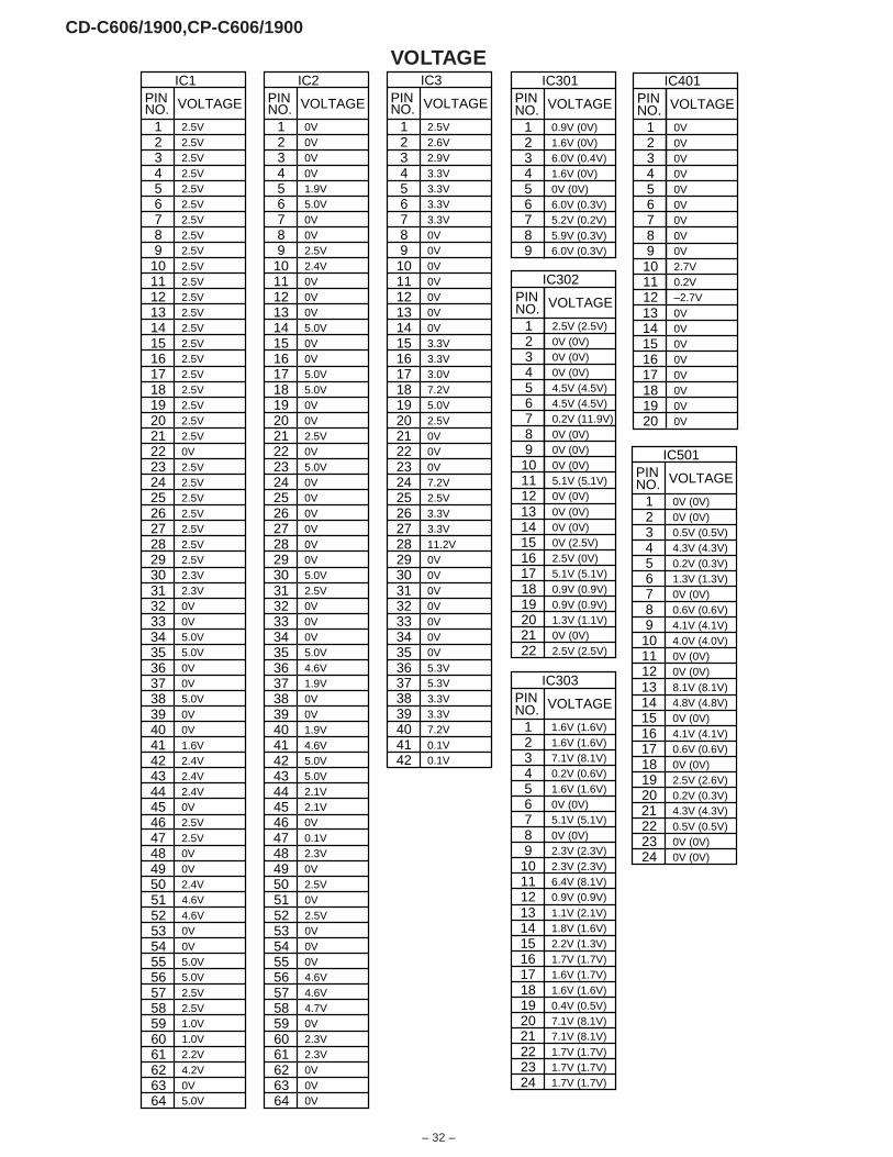
CD-C606/1900,CP-C606/1900
– 32 –
VOLTAGE
11.2V
0V0V0V2.5V
3.0V3.3V
0V
0V0V0V0V
3.3V3.3V3.3V
2.5V2.6V2.9V3.3V
0V
0V
3.3V
7.2V5.0V
7.2V2.5V3.3V3.3V
0V0V0V0V0V0V0V5.3V
987654321
302928272625242322212019181716151413121110
363534333231
5.3V3.3V3.3V7.2V0.1V410.1V42
40393837
PINNO. VOLTAGE
IC3
0V
0V
0V0V0V0V
0V
0V0V2.7V0.2V–2.7V
987654321
121110
0V
0V0V
0V0V0V0V0V
1716151413
201918
PINNO. VOLTAGE
IC401
5.1V (5.1V)
1.6V (1.6V)
1.6V (1.6V)1.6V (1.6V)7.1V (8.1V)0.2V (0.6V)
0V (0V)
0V (0V)2.3V (2.3V)2.3V (2.3V)6.4V (8.1V)0.9V (0.9V)
987654321
121110
2.2V (1.3V)
1.1V (2.1V)1.8V (1.6V)
1.7V (1.7V)1.6V (1.7V)1.6V (1.6V)0.4V (0.5V)7.1V (8.1V)
1716151413
201918
7.1V (8.1V)1.7V (1.7V)1.7V (1.7V)1.7V (1.7V)
21
242322
PINNO. VOLTAGE
IC303
0.2V (11.9V)
4.5V (4.5V)
2.5V (2.5V)0V (0V)0V (0V)0V (0V)
4.5V (4.5V)
0V (0V)0V (0V)0V (0V)5.1V (5.1V)0V (0V)
987654321
121110
0V (2.5V)
0V (0V)0V (0V)
2.5V (0V)5.1V (5.1V)0.9V (0.9V)0.9V (0.9V)1.3V (1.1V)
1716151413
201918
0V (0V)2.5V (2.5V)
2122
PINNO. VOLTAGE
IC302
5.2V (0.2V)
0V (0V)
0.9V (0V)1.6V (0V)6.0V (0.4V)1.6V (0V)
6.0V (0.3V)
5.9V (0.3V)6.0V (0.3V)9
87654321
PINNO. VOLTAGE
IC301
0V
2.1V5.0V5.0V4.6V1.9V
0V
5.0V0V2.5V0V
5.0V0V
5.0V
0V0V2.4V2.5V
0V5.0V1.9V
0V2.3V2.3V0V4.7V
4.6V
0V0V0V0V
0V
0V
0V
5.0V0V
0V0V0V0V
0V5.0V2.5V0V0V0V5.0V4.6V1.9V0V0V
2.1V
0.1V2.3V0V2.5V0V2.5V0V0V0V
4.6V
0V0V
987654321
302928272625242322212019181716151413121110
5049484746454443424140393837363534333231
PINNO. VOLTAGE
51
64636261605958575655545352
IC2
0V (0V)
0.2V (0.3V)
0V (0V)0V (0V)0.5V (0.5V)4.3V (4.3V)
1.3V (1.3V)
0.6V (0.6V)4.1V (4.1V)4.0V (4.0V)0V (0V)0V (0V)
987654321
121110
0V (0V)
8.1V (8.1V)4.8V (4.8V)
4.1V (4.1V)0.6V (0.6V)0V (0V)2.5V (2.6V)0.2V (0.3V)
1716151413
201918
4.3V (4.3V)0.5V (0.5V)0V (0V)0V (0V)
21
242322
PINNO. VOLTAGE
IC501
2.5V
2.4V2.4V2.4V1.6V0V
2.5V
2.5V0V2.5V2.5V
2.5V2.5V
2.5V
2.5V2.5V2.5V2.5V
2.5V2.5V2.5V
4.2V2.2V1.0V1.0V2.5V
5.0V
2.5V2.5V2.5V2.5V
2.5V
2.5V
2.5V
2.5V2.5V
2.5V2.5V2.5V2.5V
2.5V2.3V2.3V0V0V5.0V5.0V0V0V5.0V0V
0V
2.5V0V0V2.4V4.6V4.6V0V0V5.0V
2.5V
0V5.0V
987654321
302928272625242322212019181716151413121110
5049484746454443424140393837363534333231
PINNO. VOLTAGE
51
64636261605958575655545352
IC1
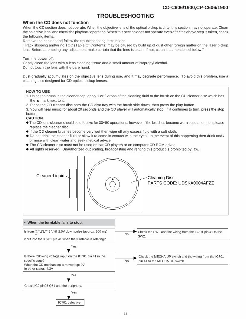
CD-C606/1900,CP-C606/1900
– 33 –
TROUBLESHOOTING
• When the turntable fails to stop.
Is from 5 V till 2.5V down pulse (approx. 300 ms) Check the SW2 and the wiring from the IC701 pin 41 to theSW2.
No
input into the IC701 pin 41 when the turntable is rotating?
5V
2.5V
Yes
Check IC2 pin26 Q51 and the periphery.
Check the MECHA UP switch and the wiring from the IC701pin 41 to the MECHA UP switch.No
Yes
Is there following voltage input on the IC701 pin 41 in thespecific state?When the CD mechanism is moved up: 0VIn other states: 4.3V
Yes
IC701 defective.
When the CD does not functionWhen the CD section does not operate. When the objective lens of the optical pickup is dirty, this section may not operate. Cleanthe objective lens, and check the playback operation. When this section does not operate even after the above step is taken, checkthe following items.Remove the cabinet and follow the troubleshooting instructions."Track skipping and/or no TOC (Table Of Contents) may be caused by build up of dust other foreign matter on the laser pickuplens. Before attempting any adjustment make certain that the lens is clean. If not, clean it as mentioned below."
Turn the power off.Gently clean the lens with a lens cleaning tissue and a small amount of isopropyl alcohol.Do not touch the lens with the bare hand.
Dust gradually accumulates on the objective lens during use, and it may degrade performance. To avoid this problem, use acleaning disc designed for CD optical pickup lenses.
0V
HOW TO USE1. Using the brush in the cleaner cap, apply 1 or 2 drops of the cleaning fluid to the brush on the CD cleaner disc which has
the mark next to it.2. Place the CD cleaner disc onto the CD disc tray with the brush side down, then press the play button.3. You will hear music for about 20 seconds and the CD player will automatically stop. If it continues to turn, press the stopbutton.CAUTION
The CD lens cleaner should be effective for 30~50 operations, however if the brushes become worn out earller then pleasereplace the cleaner disc.
If the CD cleaner brushes become very wet then wipe off any excess fluid with a soft cloth. Do not drink the cleaner fluid or allow it to come in contact with the eyes. In the event of this happening then drink and /or rinse with clean water and seek medical advice. The CD cleaner disc must not be used on car CD players or on computer CD ROM drives. All rights reserved. Unauthorized duplicating, broadcasting and renting this product is prohibited by law.
Cleaner Liquid Cleaning DiscPARTS CODE: UDSKA0004AFZZ
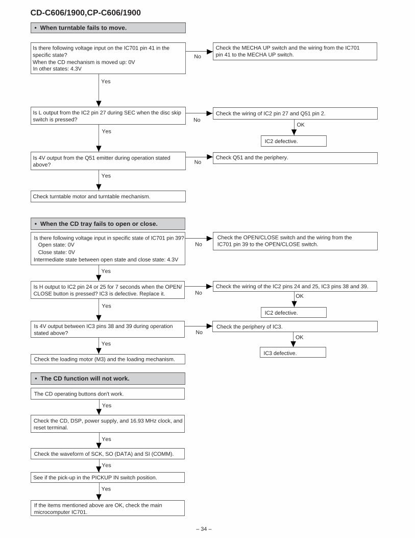
CD-C606/1900,CP-C606/1900
– 34 –
• When the CD tray fails to open or close.
Is there following voltage input in specific state of IC701 pin 39? Open state: 0V Close state: 0V Intermediate state between open state and close state: 4.3V
Is H output to IC2 pin 24 or 25 for 7 seconds when the OPEN/CLOSE button is pressed? IC3 is defective. Replace it.
Is 4V output between IC3 pins 38 and 39 during operationstated above?
Check the loading motor (M3) and the loading mechanism.
Yes
Yes
Yes
No
No
IC2 defective.
NoCheck the periphery of IC3.
IC3 defective.
OK
OK
Check the OPEN/CLOSE switch and the wiring from theIC701 pin 39 to the OPEN/CLOSE switch.
Check the wiring of the IC2 pins 24 and 25, IC3 pins 38 and 39.
• The CD function will not work.
The CD operating buttons don't work.
Check the CD, DSP, power supply, and 16.93 MHz clock, andreset terminal.
Check the waveform of SCK, SO (DATA) and SI (COMM).
Yes
Yes
See if the pick-up in the PICKUP IN switch position.
If the items mentioned above are OK, check the mainmicrocomputer IC701.
Yes
Yes
No
Is there following voltage input on the IC701 pin 41 in thespecific state?
In other states: 4.3VWhen the CD mechanism is moved up: 0V
• When turntable fails to move.
Check the MECHA UP switch and the wiring from the IC701pin 41 to the MECHA UP switch.
Is 4V output from the Q51 emitter during operation statedabove?
Yes
Yes
Check the wiring of IC2 pin 27 and Q51 pin 2.
OKNo
No
Is L output from the IC2 pin 27 during SEC when the disc skipswitch is pressed?
Yes
Check turntable motor and turntable mechanism.
Check Q51 and the periphery.
IC2 defective.
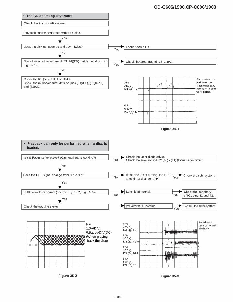
CD-C606/1900,CP-C606/1900
– 35 –
• Playback can only be performed when a disc isloaded.
Is HF waveform normal (see the Fig. 35-2, Fig. 35-3)?
Check the tracking system.
Is the Focus servo active? (Can you hear it working?) Check the laser diode driver.Check the area around IC1(16) - (21) (focus servo circuit).No
Yes
Yes
Yes
Does the DRF signal change from "L" to "H"?No Yes
If the disc is not turning, the DRFshould not change to "H".
Level is abnormal.No Yes
Waveform is unstable. Check the spin system.Yes
Check the peripheryof IC1 pins 41 and 42.
Check the spin system.
Figure 35-3Figure 35-2
HF1.0V/DIV0.5µsec/DIV(DC)(When playing back the disc)
3
21
4
0.5s1.00 VIC1 16 FD
0.5s10.0 VIC2 12 CLV+
0.5s10.0 VIC1 54 DRF
0.5s2.00 VIC1 7 TE
Waveform incase of normalplayback
No
Yes
No
• The CD operating keys work.
Check the Focus - HF system.
Playback can be performed without a disc.
Focus search OKDoes the pick-up move up and down twice?
Does the output waveform of IC1(16)(FD) match that shown inFig. 35-1?
Check the IC1(50)(CLK) line, 4MHz.Check the microcomputer data on pins (51)(CL), (52)(DAT)and (53)CE.
Check the area around IC3-CNP2.Yes
Yes
Figure 35-1
0.5s0.50 VIC1 16 FD
2
1
0.5s0.50 VIC1 7 TE
Focus search is performed two times when play operation is done without disc.
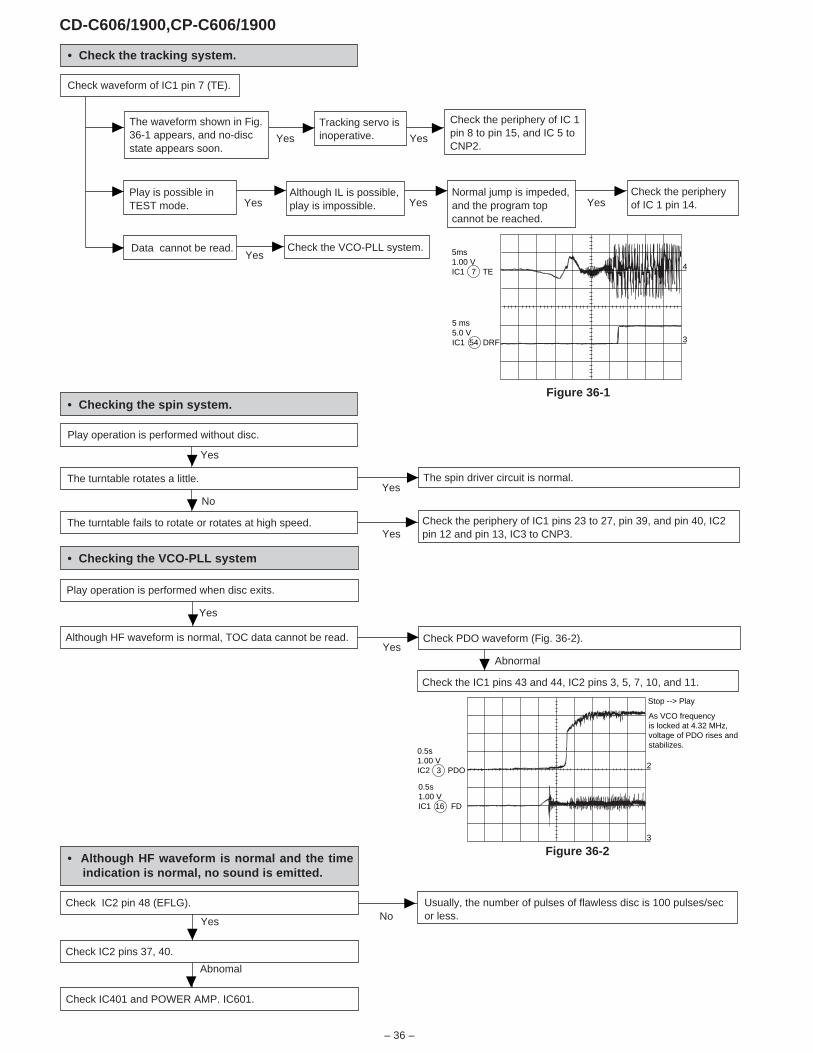
CD-C606/1900,CP-C606/1900
– 36 –
• Checking the spin system.
Yes
No
Play operation is performed without disc.
The turntable rotates a little.
The turntable fails to rotate or rotates at high speed.
YesThe spin driver circuit is normal.
Check the periphery of IC1 pins 23 to 27, pin 39, and pin 40, IC2pin 12 and pin 13, IC3 to CNP3.Yes
• Checking the VCO-PLL system
Figure 36-2
Play operation is performed when disc exits.
Yes
Although HF waveform is normal, TOC data cannot be read.Yes
Check PDO waveform (Fig. 36-2).
Abnormal
Check the IC1 pins 43 and 44, IC2 pins 3, 5, 7, 10, and 11.
• Although HF waveform is normal and the timeindication is normal, no sound is emitted.
Check IC2 pin 48 (EFLG).
Check IC2 pins 37, 40.
Check IC401 and POWER AMP. IC601.
Abnomal
Yes
Usually, the number of pulses of flawless disc is 100 pulses/secor less.No
2
3
0.5s1.00 VIC2 3 PDO
0.5s1.00 VIC1 16 FD
As VCO frequencyis locked at 4.32 MHz, voltage of PDO rises andstabilizes.
Stop --> Play
• Check the tracking system.
Check waveform of IC1 pin 7 (TE).
Play is possible inTEST mode.
Although IL is possible,play is impossible.
Check the peripheryof IC 1 pin 14.
Normal jump is impeded,and the program topcannot be reached.
Check the periphery of IC 1pin 8 to pin 15, and IC 5 toCNP2.
The waveform shown in Fig.36-1 appears, and no-discstate appears soon.
Tracking servo isinoperative.
Yes YesYes
YesYes
Data cannot be read. Check the VCO-PLL system.Yes
Figure 36-1
3
4
5ms1.00 VIC1 7 TE
5 ms5.0 VIC1 54 DRF
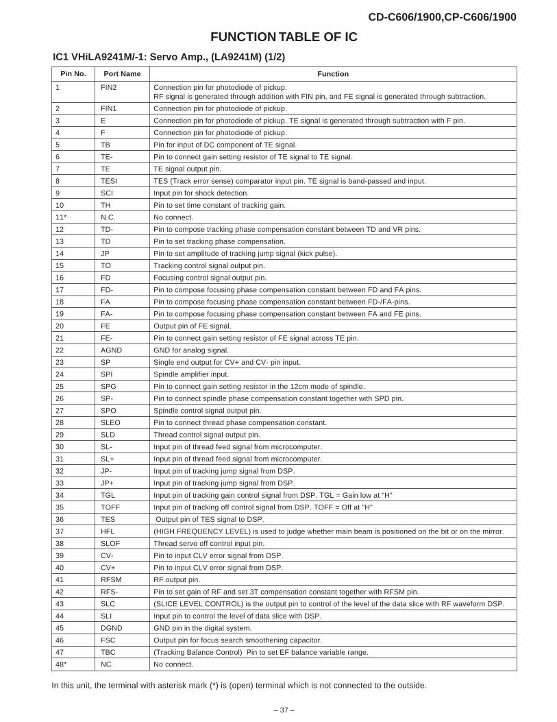
CD-C606/1900,CP-C606/1900
– 37 –
IC1 VHiLA9241M/-1: Servo Amp., (LA9241M) (1/2)
1 FIN2 Connection pin for photodiode of pickup.RF signal is generated through addition with FIN pin, and FE signal is generated through subtraction.
2 FIN1 Connection pin for photodiode of pickup.
3 E Connection pin for photodiode of pickup. TE signal is generated through subtraction with F pin.
4 F Connection pin for photodiode of pickup.
5 TB Pin for input of DC component of TE signal.
6 TE- Pin to connect gain setting resistor of TE signal to TE signal.
7 TE TE signal output pin.
8 TESI TES (Track error sense) comparator input pin. TE signal is band-passed and input.
9 SCI Input pin for shock detection.
10 TH Pin to set time constant of tracking gain.
11* N.C. No connect.
12 TD- Pin to compose tracking phase compensation constant between TD and VR pins.
13 TD Pin to set tracking phase compensation.
14 JP Pin to set amplitude of tracking jump signal (kick pulse).
15 TO Tracking control signal output pin.
16 FD Focusing control signal output pin.
17 FD- Pin to compose focusing phase compensation constant between FD and FA pins.
18 FA Pin to compose focusing phase compensation constant between FD-/FA-pins.
19 FA- Pin to compose focusing phase compensation constant between FA and FE pins.
20 FE Output pin of FE signal.
21 FE- Pin to connect gain setting resistor of FE signal across TE pin.
22 AGND GND for analog signal.
23 SP Single end output for CV+ and CV- pin input.
24 SPI Spindle amplifier input.
25 SPG Pin to connect gain setting resistor in the 12cm mode of spindle.
26 SP- Pin to connect spindle phase compensation constant together with SPD pin.
27 SPO Spindle control signal output pin.
28 SLEO Pin to connect thread phase compensation constant.
29 SLD Thread control signal output pin.
30 SL- Input pin of thread feed signal from microcomputer.
31 SL+ Input pin of thread feed signal from microcomputer.
32 JP- Input pin of tracking jump signal from DSP.
33 JP+ Input pin of tracking jump signal from DSP.
34 TGL Input pin of tracking gain control signal from DSP. TGL = Gain low at "H"
35 TOFF Input pin of tracking off control signal from DSP. TOFF = Off at "H"
36 TES Output pin of TES signal to DSP.
37 HFL (HIGH FREQUENCY LEVEL) is used to judge whether main beam is positioned on the bit or on the mirror.
38 SLOF Thread servo off control input pin.
39 CV- Pin to input CLV error signal from DSP.
40 CV+ Pin to input CLV error signal from DSP.
41 RFSM RF output pin.
42 RFS- Pin to set gain of RF and set 3T compensation constant together with RFSM pin.
43 SLC (SLICE LEVEL CONTROL) is the output pin to control of the level of the data slice with RF waveform DSP.
44 SLI Input pin to control the level of data slice with DSP.
45 DGND GND pin in the digital system.
46 FSC Output pin for focus search smoothening capacitor.
47 TBC (Tracking Balance Control) Pin to set EF balance variable range.
48* NC No connect.
Pin No. Port Name Function
In this unit, the terminal with asterisk mark (*) is (open) terminal which is not connected to the outside.
FUNCTION TABLE OF IC
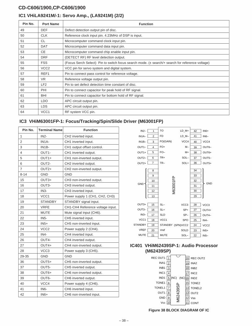
CD-C606/1900,CP-C606/1900
– 38 –
IC1 VHiLA9241M/-1: Servo Amp., (LA9241M) (2/2)
Pin No. Port Name Function
49 DEF Defect detection output pin of disc.
50 CLK Reference clock input pin. 4.23MHz of DSP is input.
51 CL Microcomputer command clock input pin.
52 DAT Microcomputer command data input pin.
53 CE Microcomputer command chip enable input pin.
54 DRF (DETECT RF) RF level detection output.
55 FSS (Focus Serch Select) Pin to switch focus search mode. (± search/+ search for reference voltage)
56 VCC2 VCC pin for servo system and digital system.
57 REF1 Pin to connect pass control for reference voltage.
58 VR Reference voltage output pin.
59 LF2 Pin to set defect detection time constant of disc.
60 PHI Pin to connect capacitor for peak hold of RF signal.
61 BHI Pin to connect capacitor for bottom hold of RF signal.
62 LDO APC circuit output pin.
63 LDS APC circuit output pin.
64 VCC1 RF system VCC pin.
Figure 38 BLOCK DIAGRAM OF IC
IC3 VHiM63001FP-1: Focus/Tracking/Spin/Slide Driver (M63001FP)
IC401 VHiM62439SP-1: Audio Processor (M62439SP)
1
2
3
4
5
6
7
15
16
17
18
19
20
21
28
36
37
38
39
40
41
42
27
26
25
24
23
22
IN2–
IN1A–
IN1B–
OUT1–
OUT1+
OUT2–
OUT2+
OUT3+
OUT3–
IN3–
VCC1
STANDBY
VREF
MUTE
GND GND
VCC3
OUT4+
OUT4–
IN4–
VCC2
IN5+
IN5–
IN6+
IN6–
VCC4
OUT6–
OUT6+
OUT5–
OUT5+
8
9
10
11
12
13
34
33
32
31
30
29
TO
FD
FO(GAIN)
FO+
FO–
TR+
TR–
SL–
SL+
SLD
VCC1
STANDBY
Vref
MUTE
LD_M+
LD_M–
VCC4
M–
M+
SOL–
SOL+
VCC3
SP+
SP–
SPO
(SPN)VCC2
SOLD
SOL–
M63
001F
P
1
2
3
4
5
6
7
8
9
10 11
12
13
14
15
16
17
18
19
20
M62
439S
P
REC OUT1
INA1
INB1
INC1
IND1
TONE1
TONEL1
OUT1
GND
Vcc
REC OUT2
INA2
INB2
INC2
IND2
TONE2
TONEL2
OUT2
Vss
CONT
(NC) (NC)
Pin No. Terminal Name Function
1 IN2- CH2 inverted input.
2 IN1A- CH1 inverted input.
3 IN1B- CH1 output offset control.
4 OUT1- CH1 inverted output.
5 OUT1+ CH1 non-inverted output.
6 OUT2- CH2 inverted output.
7 OUT2+ CH2 non-inverted output.
8-14 GND GND
15 OUT3+ CH3 non-inverted output.
16 OUT3- CH3 inverted output.
17 IN3- CH3 inverted input.
18 VCC1 Power supply 1 (CH1, CH2, CH3)
19 STANDBY STANDBY signal input.
20 VRFE CH1-CH4 Reference voltage input.
21 MUTE Mute signal input (CH6).
22 IN5- CH5 inverted input.
23 IN5+ CH5 non-inverted input.
24 VCC2 Power supply 2 (CH4).
25 IN4- CH4 inverted input.
26 OUT4- CH4 inverted output.
27 OUT4+ CH4 non-inverted output.
28 VCC3 Power supply 3 (CH5).
29-35 GND GND
36 OUT5+ CH5 non-inverted output.
37 OUT5- CH5 inverted output.
38 OUT6+ CH6 non-inverted output.
39 OUT6- CH6 inverted output.
40 VCC4 Power supply 4 (CH6).
41 IN6- CH6 inverted input.
42 IN6+ CH6 non-inverted input.
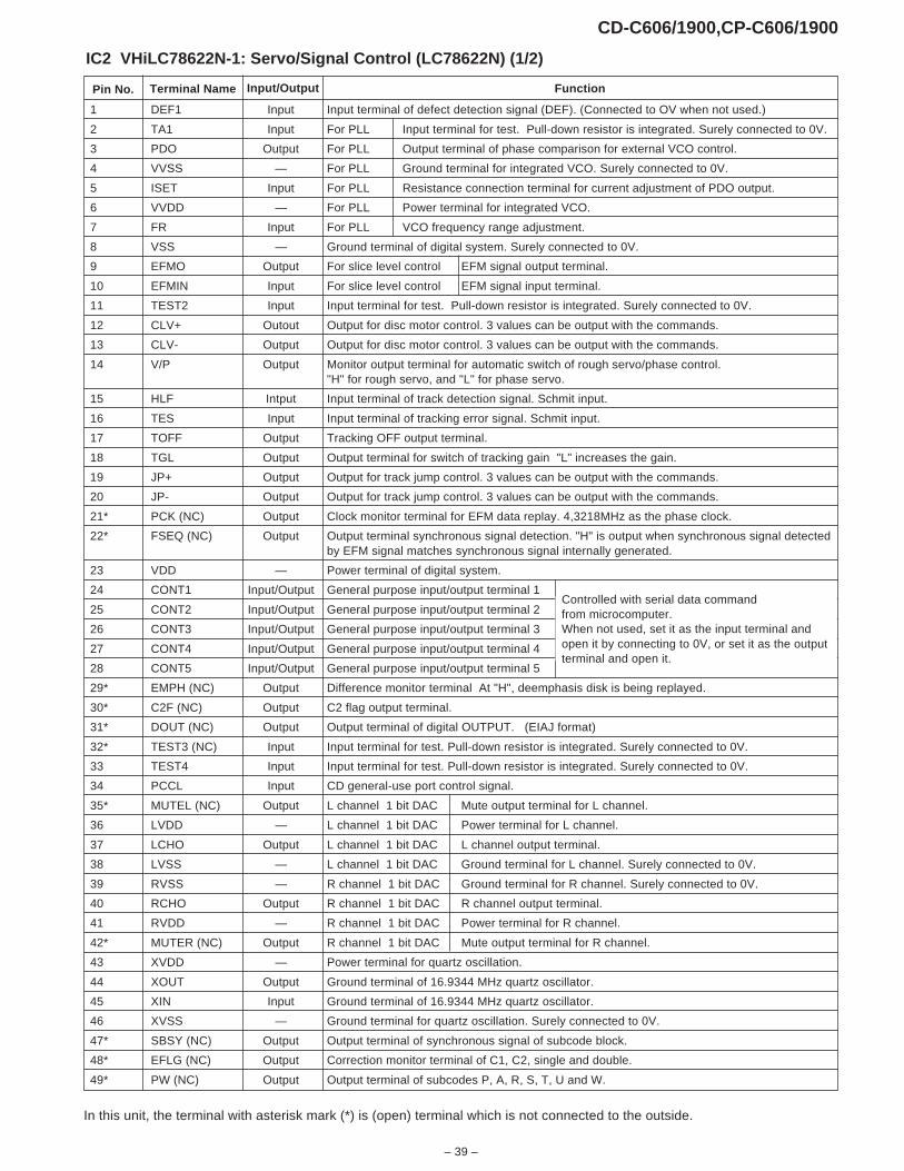
CD-C606/1900,CP-C606/1900
– 39 –
1 DEF1 Input Input terminal of defect detection signal (DEF). (Connected to OV when not used.)
2 TA1 Input For PLL Input terminal for test. Pull-down resistor is integrated. Surely connected to 0V.
3 PDO Output For PLL Output terminal of phase comparison for external VCO control.
4 VVSS — For PLL Ground terminal for integrated VCO. Surely connected to 0V.
5 ISET Input For PLL Resistance connection terminal for current adjustment of PDO output.
6 VVDD — For PLL Power terminal for integrated VCO.
7 FR Input For PLL VCO frequency range adjustment.
8 VSS — Ground terminal of digital system. Surely connected to 0V.
9 EFMO Output For slice level control EFM signal output terminal.
10 EFMIN Input For slice level control EFM signal input terminal.
11 TEST2 Input Input terminal for test. Pull-down resistor is integrated. Surely connected to 0V.
12 CLV+ Outout Output for disc motor control. 3 values can be output with the commands.
13 CLV- Output Output for disc motor control. 3 values can be output with the commands.
14 V/P Output Monitor output terminal for automatic switch of rough servo/phase control."H" for rough servo, and "L" for phase servo.
15 HLF Intput Input terminal of track detection signal. Schmit input.
16 TES Input Input terminal of tracking error signal. Schmit input.
17 TOFF Output Tracking OFF output terminal.
18 TGL Output Output terminal for switch of tracking gain "L" increases the gain.
19 JP+ Output Output for track jump control. 3 values can be output with the commands.
20 JP- Output Output for track jump control. 3 values can be output with the commands.
21* PCK (NC) Output Clock monitor terminal for EFM data replay. 4,3218MHz as the phase clock.
22* FSEQ (NC) Output Output terminal synchronous signal detection. "H" is output when synchronous signal detectedby EFM signal matches synchronous signal internally generated.
23 VDD — Power terminal of digital system.
24 CONT1 Input/Output General purpose input/output terminal 1
25 CONT2 Input/Output General purpose input/output terminal 2
26 CONT3 Input/Output General purpose input/output terminal 3
27 CONT4 Input/Output General purpose input/output terminal 4
28 CONT5 Input/Output General purpose input/output terminal 5
29* EMPH (NC) Output Difference monitor terminal At "H", deemphasis disk is being replayed.
30* C2F (NC) Output C2 flag output terminal.
31* DOUT (NC) Output Output terminal of digital OUTPUT. (EIAJ format)
32* TEST3 (NC) Input Input terminal for test. Pull-down resistor is integrated. Surely connected to 0V.
33 TEST4 Input Input terminal for test. Pull-down resistor is integrated. Surely connected to 0V.
34 PCCL Input CD general-use port control signal.
35* MUTEL (NC) Output L channel 1 bit DAC Mute output terminal for L channel.
36 LVDD — L channel 1 bit DAC Power terminal for L channel.
37 LCHO Output L channel 1 bit DAC L channel output terminal.
38 LVSS — L channel 1 bit DAC Ground terminal for L channel. Surely connected to 0V.
39 RVSS — R channel 1 bit DAC Ground terminal for R channel. Surely connected to 0V.
40 RCHO Output R channel 1 bit DAC R channel output terminal.
41 RVDD — R channel 1 bit DAC Power terminal for R channel.
42* MUTER (NC) Output R channel 1 bit DAC Mute output terminal for R channel.
43 XVDD — Power terminal for quartz oscillation.
44 XOUT Output Ground terminal of 16.9344 MHz quartz oscillator.
45 XIN Input Ground terminal of 16.9344 MHz quartz oscillator.
46 XVSS — Ground terminal for quartz oscillation. Surely connected to 0V.
47* SBSY (NC) Output Output terminal of synchronous signal of subcode block.
48* EFLG (NC) Output Correction monitor terminal of C1, C2, single and double.
49* PW (NC) Output Output terminal of subcodes P, A, R, S, T, U and W.
IC2 VHiLC78622N-1: Servo/Signal Control (LC78622N) (1/2)
Pin No. FunctionTerminal Name Input/Output
In this unit, the terminal with asterisk mark (*) is (open) terminal which is not connected to the outside.
Controlled with serial data commandfrom microcomputer.When not used, set it as the input terminal andopen it by connecting to 0V, or set it as the outputterminal and open it.
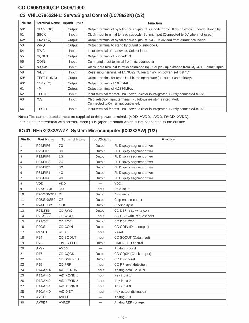
CD-C606/1900,CP-C606/1900
– 40 –
IC2 VHiLC78622N-1: Servo/Signal Control (LC78622N) (2/2)
FunctionTerminal Name Input/Output
50* SFSY (NC) Output Output terminal of synchronous signal of subcode frame. It drops when subcode stands by.
51 SBCK Input Clock input terminal to read subcode. Schmit input (Connected to 0V when not used.)
52* FSX (NC) Output Output terminal of synchronous signal of 7.35kHz divided from quartz oscillation.
53 WRQ Output Output terminal to stand by output of subcode Q.
54 RWC Input Input terminal of read/write. Schmit input.
55 SQOUT Output Output terminal of subcode Q.
56 COIN Input Command input terminal from microcomputer.
57 /CQCK Input Clock input terminal to fetch command input, or pick up subcode from SQOUT. Schmit input.
58 /RES Input Reset input terminal of LC78622. When turning on power, set it at "L".
59* TEST11 (NC) Output Output terminal for test. Used in the open state ("L" output as ordinary).
60* 16M (NC) Output Output terminal of 16.9344Hz.
61 4M Output Output terminal of 4.2336MHz.
62 TEST5 Input Input terminal for test. Pull-down resistor is integrated. Surely connected to 0V.
63 /CS Input Chip selection input terminal. Pull-down resistor is integrated.Connected to 0when not controlled.
64 TEST1 Input Input terminal for test. Pull-down resistor is integrated. Surely connected to 0V.
Pin No.
Note: The same potential must be supplied to the power terminals (VDD, VVDD, LVDD, RVDD, XVDD).In this unit, the terminal with asterisk mark (*) is (open) terminal which is not connected to the outside.
1 P94/FIP6 7G Output FL Display segment driver
2 P93/FIP5 8G Output FL Display segment driver
3 P92/FIP4 1G Output FL Display segment driver
4 P91/FIP3 2G Output FL Display segment driver
5 P90/FIP2 3G Output FL Display segment driver
6 P81/FIP1 4G Output FL Display segment driver
7 P80/FIP0 9G Output FL Display segment driver
8 VDD VDD — VDD
9 P27/SCK0 DO Input Data input
10 P26/S00/SB1 DI Output Data output
11 P25/SI0/SB0 CE Output Chip enable output
12 P24/BUSY CLK Output Clock output
13 P23/STB CD RWC Output CD DSP read write cont
14 P22/SCK1 CD WRQ Input CD DSP write request cont
15 P21/S01 CD PCCL Output CD DSP PCCL
16 P20/SI1 CD COIN Output CD COIN (Data output)
17 RESET RESET Input Reset
18 P74 CD SQOUT Input CD SQOUT (Data input)
19 P73 TIMER LED Output TIMER LED control
20 AVss AVSS — Analog ground
21 P17 CD CQCK Output CD CQCK (Clock output)
22 P16 CD DSP RES Output CD DSP reset
23 P15 CD FRF Input CD RF level detection
24 P14/ANI4 A/D T2 RUN Input Analog data T2 RUN
25 P13/ANI3 A/D KEYIN 1 Input Key input 1
26 P12/ANI2 A/D KEYIN 2 Input Key input 2
27 P11/ANI1 A/D KEYIN 3 Input Key input 3
28 P10/ANI0 A/D DIST Input Key output distination
29 AVDD AVDD — Analog VDD
30 AVREF AVREF — Analog REF voltage
IC701 RH-iX0282AWZZ: System Microcomputer (IX0282AW) (1/2)
Port Name Terminal NamePin No. Input/Output Function
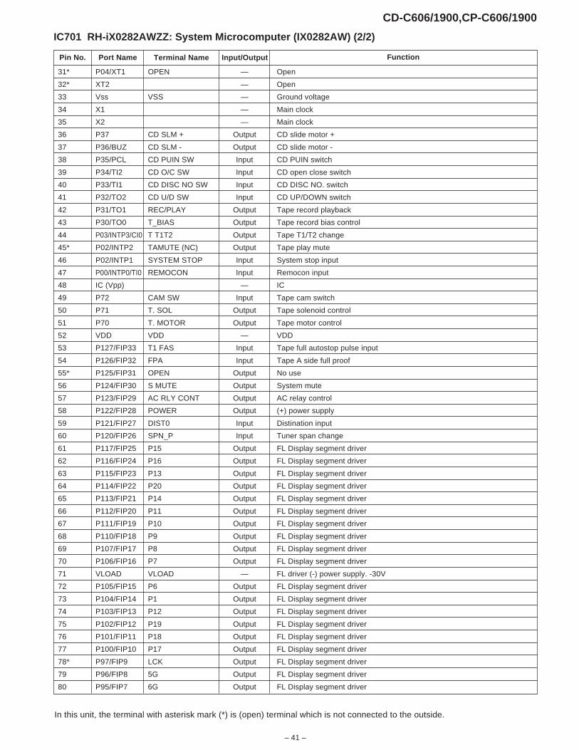
CD-C606/1900,CP-C606/1900
– 41 –
31* P04/XT1 OPEN — Open
32* XT2 — Open
33 Vss VSS — Ground voltage
34 X1 — Main clock
35 X2 — Main clock
36 P37 CD SLM + Output CD slide motor +
37 P36/BUZ CD SLM - Output CD slide motor -
38 P35/PCL CD PUIN SW Input CD PUIN switch
39 P34/TI2 CD O/C SW Input CD open close switch
40 P33/TI1 CD DISC NO SW Input CD DISC NO. switch
41 P32/TO2 CD U/D SW Input CD UP/DOWN switch
42 P31/TO1 REC/PLAY Output Tape record playback
43 P30/TO0 T_BIAS Output Tape record bias control
44 P03/INTP3/CI0 T T1T2 Output Tape T1/T2 change
45* P02/INTP2 TAMUTE (NC) Output Tape play mute
46 P02/INTP1 SYSTEM STOP Input System stop input
47 P00/INTP0/TI0 REMOCON Input Remocon input
48 IC (Vpp) — IC
49 P72 CAM SW Input Tape cam switch
50 P71 T. SOL Output Tape solenoid control
51 P70 T. MOTOR Output Tape motor control
52 VDD VDD — VDD
53 P127/FIP33 T1 FAS Input Tape full autostop pulse input
54 P126/FIP32 FPA Input Tape A side full proof
55* P125/FIP31 OPEN Output No use
56 P124/FIP30 S MUTE Output System mute
57 P123/FIP29 AC RLY CONT Output AC relay control
58 P122/FIP28 POWER Output (+) power supply
59 P121/FIP27 DIST0 Input Distination input
60 P120/FIP26 SPN_P Input Tuner span change
61 P117/FIP25 P15 Output FL Display segment driver
62 P116/FIP24 P16 Output FL Display segment driver
63 P115/FIP23 P13 Output FL Display segment driver
64 P114/FIP22 P20 Output FL Display segment driver
65 P113/FIP21 P14 Output FL Display segment driver
66 P112/FIP20 P11 Output FL Display segment driver
67 P111/FIP19 P10 Output FL Display segment driver
68 P110/FIP18 P9 Output FL Display segment driver
69 P107/FIP17 P8 Output FL Display segment driver
70 P106/FIP16 P7 Output FL Display segment driver
71 VLOAD VLOAD — FL driver (-) power supply. -30V
72 P105/FIP15 P6 Output FL Display segment driver
73 P104/FIP14 P1 Output FL Display segment driver
74 P103/FIP13 P12 Output FL Display segment driver
75 P102/FIP12 P19 Output FL Display segment driver
76 P101/FIP11 P18 Output FL Display segment driver
77 P100/FIP10 P17 Output FL Display segment driver
78* P97/FIP9 LCK Output FL Display segment driver
79 P96/FIP8 5G Output FL Display segment driver
80 P95/FIP7 6G Output FL Display segment driver
IC701 RH-iX0282AWZZ: System Microcomputer (IX0282AW) (2/2)
Port Name Terminal NamePin No. Input/Output Function
In this unit, the terminal with asterisk mark (*) is (open) terminal which is not connected to the outside.
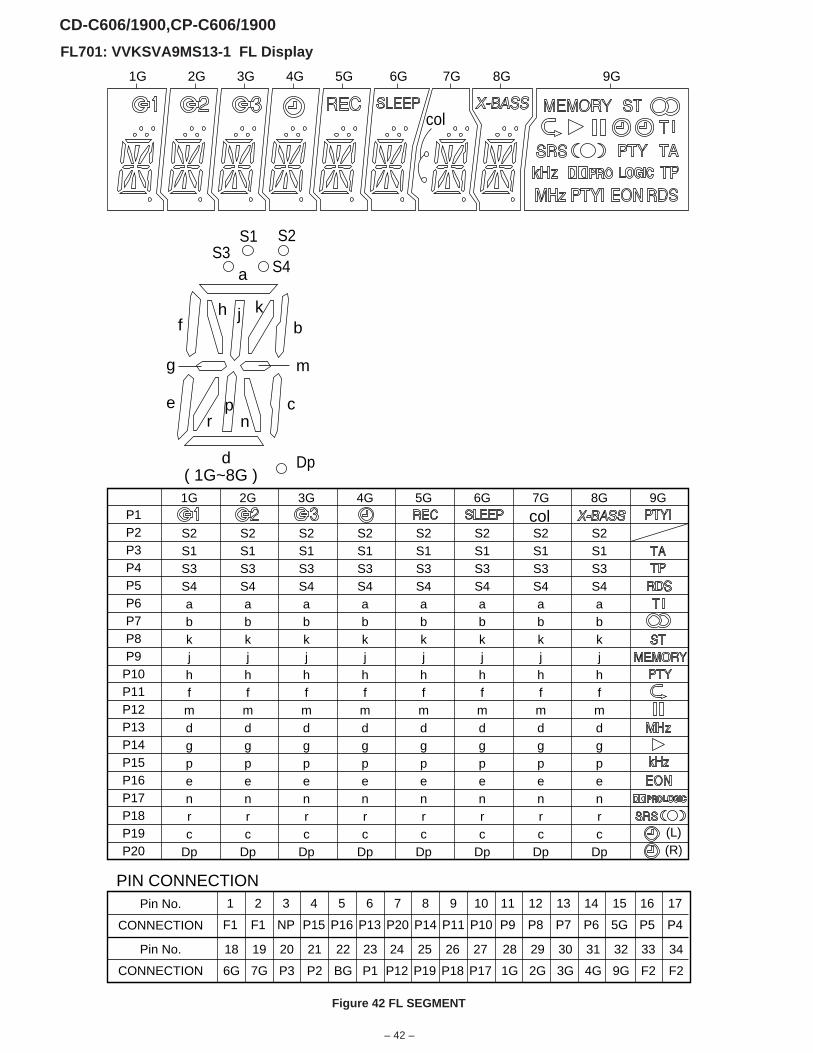
CD-C606/1900,CP-C606/1900
– 42 –
FL701: VVKSVA9MS13-1 FL Display
Figure 42 FL SEGMENT
P1P2P3P4P5P6P7P8P9P10P11P12P13P14P15P16P17P18P19P20
1G
S2S1S3S4abkjhfmdgpenrc
Dp
2G
S2S1S3S4abkjhfmdgpenrc
Dp
3G
S2S1S3S4abkjhfmdgpenrc
Dp
4G
S2S1S3S4abkjhfmdgpenrc
Dp
5G
S2S1S3S4abkjhfmdgpenrc
Dp
6G
S2S1S3S4abkjhfmdgpenrc
Dp
7G
S2S1S3S4abkjhfmdgpenrc
Dp
8G
S2S1S3S4abkjhfmdgpenrc
Dp
9G
Pin No.
CONNECTION
Pin No.
CONNECTION
17
P4
16
P5
18
6G
19
7G
20
P3
21
P2
22
BG
23
P1
24
P12
25
P19
26
P18
27
P17
28
1G
29
2G
30
3G
31
4G
32
9G
33
F2
34
F2
1
F1
2
F1
3
NP
4
P15
5
P16
6
P13
7
P20
8
P14
9
P11
10
P10
11
P9
12
P8
13
P7
14
P6
15
5G
PIN CONNECTION
2G 3G 4G 5G 6G 7G 8G 9G1G
a
b
c
d
f
g m
er
pn
h j k
( 1G~8G )
col
S3S1 S2
S4
Dp
col
(L)(R)
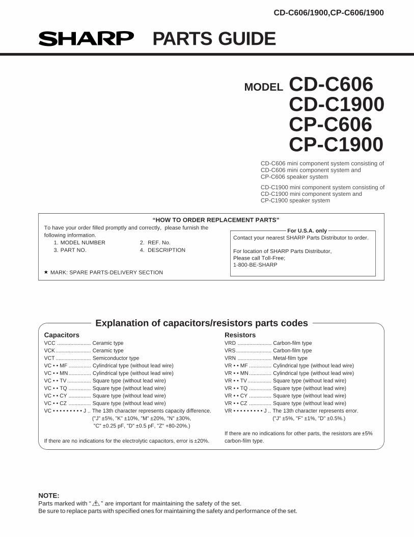
CD-C606/1900,CP-C606/1900
– 39 –
PARTS GUIDE
NOTE:Parts marked with “ ” are important for maintaining the safety of the set.Be sure to replace parts with specified ones for maintaining the safety and performance of the set.
MODEL CD-C606CD-C1900CP-C606CP-C1900
“HOW TO ORDER REPLACEMENT PARTS”To have your order filled promptly and correctly, please furnish thefollowing information.
1. MODEL NUMBER 2. REF. No.3. PART NO. 4. DESCRIPTION
MARK: SPARE PARTS-DELIVERY SECTION
Explanation of capacitors/resistors parts codesCapacitorsVCC ....................... Ceramic typeVCK........................ Ceramic typeVCT ........................ Semiconductor typeVC • • MF ............... Cylindrical type (without lead wire)VC • • MN ............... Cylindrical type (without lead wire)VC • • TV ................ Square type (without lead wire)VC • • TQ ............... Square type (without lead wire)VC • • CY ............... Square type (without lead wire)VC • • CZ ............... Square type (without lead wire)VC • • • • • • • • • J .. The 13th character represents capacity difference.
("J" ±5%, "K" ±10%, "M" ±20%, "N" ±30%, "C" ±0.25 pF, "D" ±0.5 pF, "Z" +80-20%.)
If there are no indications for the electrolytic capacitors, error is ±20%.
ResistorsVRD ....................... Carbon-film typeVRS........................ Carbon-film typeVRN ....................... Metal-film typeVR • • MF ............... Cylindrical type (without lead wire)VR • • MN ............... Cylindrical type (without lead wire)VR • • TV ................ Square type (without lead wire)VR • • TQ ............... Square type (without lead wire)VR • • CY ............... Square type (without lead wire)VR • • CZ ............... Square type (without lead wire)VR • • • • • • • • • J .. The 13th character represents error.
("J" ±5%, "F" ±1%, "D" ±0.5%.)
If there are no indications for other parts, the resistors are ±5%carbon-film type.
For U.S.A. onlyContact your nearest SHARP Parts Distributor to order.
For location of SHARP Parts Distributor,Please call Toll-Free;1-800-BE-SHARP
CD-C606 mini component system consisting ofCD-C606 mini component system andCP-C606 speaker system
CD-C1900 mini component system consisting ofCD-C1900 mini component system andCP-C1900 speaker system

PRICERANK
DESCRIPTIONNO. PARTS CODE NO. PARTS CODE PRICERANK DESCRIPTION
CD-C606/1900,CP-C606/1900
– 1 –
CD-C606/1900
INTEGRATED CIRCUITS
IC1 VHILA9241M/-1 J AS Servo Amp.,LA9241MIC2 VHILC78622N-1 J AY Servo/Signal Control,LC78622NIC3 VHIM63001FP-1 J AX Focus/Tracking/Spin/Slide
Driver,M63001FPIC301 VHITA7358AP-1 J AG FM Front End,TA7358APIC302 VHILC72131/-1 J AP PLL Controller,LC72131IC303 VHILA1805//-1 J AM FM IF DET./FM MPX./AM IF,
LA1805IC401 VHIM62439SP-1 J AG Audio Processor,M62439SPIC501 VHIAN7345K/-1 J AM Playback and Record/Playback
Amp.,AN7345KIC601 VHILA4282//-1 J AM Power Amp.,LA4282IC701 RH-IX0282AWZZ J AP System Microcomputer,
IX0282AWIC702 VHIKIA7042P-1 J AG Reset,KIA7042PIC901 VHIAN78L05/-1 J AE Constant Voltage Regulator,
AN78L05IC902 VHIKIA7806P-1 J AG Voltage Regulator,KIA7806PIC903 VHIKIA7812P-1 J AE Voltage Regulator,KIA7812PIC904 VHIAN78L05/-1 J AE Constant Voltage Regulator,
AN78L05
TRANSISTORS
Q1 VS2SA1318//-1 J AC Silicon,PNP,2SA1318Q51 VSKRC102M//-1 J AC Digital,NPN,KRC102 MQ52 VSKTC3203Y/-1 J AC Silicon,NPN,KTC3203 YQ301 VSKTC3194Y/-1 J AD Silicon,NPN,KTC3194 YQ351 VSKRA102M//-1 J AC Digital,PNP,KRA102 MQ381 VSKRA109M//-1 J AC Digital,PNP,KRA109 MQ401,402 VSKTC3199GR-1 J AB Silicon,NPN,KTC3199 GRQ501 VSKTA1266GR-1 J AB Silicon,PNP,KTA1266 GRQ502~505 VS2SC2389SE-1 J AD Silicon,NPN,2SC2389 SEQ506,507 VSKTC3199GR-1 J AB Silicon,NPN,KTC3199 GRQ508,509 VSKRC104M//-1 J AC Digital,NPN,KRC104 MQ512,513 VSKTC3199GR-1 J AB Silicon,NPN,KTC3199 GRQ514 VSKTA1266GR-1 J AB Silicon,PNP,KTA1266 GRQ515 VSKRC104M//-1 J AC Digital,NPN,KRC104 MQ516 VSKTC3203Y/-1 J AC Silicon,NPN,KTC3203 YQ631,632 VSKRC102M//-1 J AC Digital,NPN,KRC102 MQ701 VSKTA1273Y/-1 J AE Silicon,PNP,KTA1273 YQ702 VSKTA1271Y/-1 J AC Silicon,PNP,KTA1271 YQ703 VSKRC107M//-1 J AC Digital,NPN,KRC107 MQ704 VSKRC102M//-1 J AC Digital,NPN,KRC102 MQ901 VSKTA1266GR-1 J AB Silicon,PNP,KTA1266 GRQ902 VSKRC107M//-1 J AC Digital,NPN,KRC107 M
DIODES
D1 VHD1SS133//-1 J AA Silicon,1SS133D81,82 VHD1SS133//-1 J AA Silicon,1SS133D91~93 VHD1SS133//-1 J AA Silicon,1SS133D301 VHDDS1SS133-1 J AB Silicon,DS1SS133D303,304 VHDDS1SS133-1 J AB Silicon,DS1SS133D381 VHDDS1SS133-1 J AB Silicon,DS1SS133D701~705 VHDDS1SS133-1 J AB Silicon,DS1SS133D707,708 VHDDS1SS133-1 J AB Silicon,DS1SS133D743 VHDDS1SS133-1 J AB Silicon,DS1SS133D901~904 VHDDS1SS133-1 J AB Silicon,DS1SS133D905~909 VHD1N4004S/-1 J AB Silicon,1N4004SD910,911 VHDRL203F//-1 J AE Silicon,RL203FD912,913 VHD1N4004S/-1 J AB Silicon,1N4004SD914,915 VHDRL203F//-1 J AE Silicon,RL203FD916,917 VHD1N4004S/-1 J AB Silicon,1N4004SD918~920 VHDDS1SS133-1 J AB Silicon,DS1SS133D921~925 VHD1SS133//-1 J AA Silicon,1SS133LED701 VHPSLI342UCJ1 J AC LED,Red,SLI342UCJ1VD301,302 VHCSVC211C/-1 J AG Variable,Capacitance,SVC211CVD303 VHDSVC348S/-1 J Silicon,SVC348SZD61 VHEMTZJ5R6B-1 J AD Zener,5.6V,MTZJ5.6BZD351 VHEDZ5R1BSB-1 J AC Zener,5.1V,DZ5.1BSBZD401,402 VHEDZ2R4BSB-1 J AB Zener,2.4V,DZ2.4BSBZD901 VHEDZ6R2BSA-1 J AB Zener,6.2V,DZ6.2BSAZD902 VHEDZ300BSB-1 J AB Zener,30V,DZ300BSB
FILTERS
BF301 RFILR0008AWZZ J AE Band Pass FilterCF301 RFILF0124AFZZ J AD FM IF,10.7 MHzCF351 92LFILTA1768A J AE AM IF
TRANSFORMERS
! PT901 RTRNP0253AWZZ J BA Power! PT902 RTRNP0239AWZZ J AP Power
T301 RCILB0060AWZZ J AC FM OscillationT302 RCILI0012AWZZ J AD FM IFT331 RCILA0052AWZZ J AE AM AntennaT333 RCILB0058AWZZ J AC AM OscillationT381 RCILI0016AFZZ J FM DetectionT382 RCILI0015AWZZ J AE AM IF
COILS
L61 VP-XHR82K0000 J AC 0.82 µH,ChokeL312 RCILR0029AWZZ J AA FM RFL317 VP-DH101K0000 J AB 100 µH,ChokeL503 VP-MK331K0000 J AB 330 µH,ChokeL701 VP-DH101K0000 J AB 100 µH,Choke
VARIABLE RESISTOR
VR381 RVR-M0025AWZZ J AC 6.8 kohms (B),Semi-VR [VCO]
VIBRATORS
XL1 92LCRSTL1746AT J AH Crystal,16.93 MHzXL353 RCRSP0002AWZZ J AH Crystal,4.5 MHzXL701 RCRSP0003AWZZ J AH Crystal,4.19MHz
CAPACITORS
C1 VCEAZA1CW476M J AB 47 µF,16V,ElectrolyticC2 VCKYTV1HB103K J AA 0.01 µF,50VC3 VCEAZA1HW105M J AB 1 µF,50V,ElectrolyticC4 VCEAZA1HW104M J AB 0.1 µF,50V,ElectrolyticC5,6 VCTYPA1CX333K J AA 0.033 µF,16VC7 VCEAZA1HW104M J AB 0.1 µF,50V,ElectrolyticC8 VCTYPA1CX683K J AA 0.068 µF,16VC9 VCTYPA1CX473K J AA 0.047 µF,16VC10 VCCSTV1HL181J J AA 180 pF,50VC11,12 VCTYPA1CX104K J AB 0.1 µF,16VC13 VCKYTV1HB331K J AA 330 pF,50VC14,15 VCKYTV1HB103K J AA 0.01 µF,50VC16 VCKYTV1HB472K J AA 0.0047 µF,50VC17 VCKYTV1HB102K J AA 0.001 µF,50VC18 VCEAZA1HW474M J AB 0.47 µF,50V,ElectrolyticC19 VCEAZA1HW105M J AB 1 µF,50V,ElectrolyticC20 VCEAZA1CW476M J AB 47 µF,16V,ElectrolyticC21 VCKYTV1HB332K J AA 0.0033 µF,50VC22 VCCSPA1HL221J J AA 220 pF,50VC23 VCKYTV1HB272K J AA 0.0027 µF,50VC24 VCCSTV1HL2R2C J AB 2.2 pF,50VC25 VCCSTV1HL270J J AA 27 pF,50VC26 VCTYPA1CX333K J AA 0.033 µF,16VC27 VCKYTV1HB102K J AA 0.001 µF,50VC28 VCTYPA1CX104K J AB 0.1 µF,16VC29 VCEAZA1HW475M J AB 4.7 µF,50V,ElectrolyticC30 VCEAZA1HW104M J AB 0.1 µF,50V,ElectrolyticC31 VCEAZA0JW227M J AC 220 µF,6.3V,ElectrolyticC32 VCKYTV1HB103K J AA 0.01 µF,50VC33 VCEAZA1HW474M J AB 0.47 µF,50V,ElectrolyticC34 VCEAZA1HW334M J AB 0.33 µF,50V,ElectrolyticC35 VCEAZA1HW105M J AB 1 µF,50V,ElectrolyticC36 VCEAZA1CW107M J AC 100 µF,16V,ElectrolyticC37 VCKZPA1HF223Z J AA 0.022 µF,50VC38 VCKYTV1HB103K J AA 0.01 µF,50VC39,40 VCTYPA1CX473K J AA 0.047 µF,16VC43 VCEAZA0JW337M J AC 330 µF,6.3V,ElectrolyticC44~47 VCCCTV1HH101J J AA 100 pF (CH),50VC48 VCCSPA1HL101J J AA 100 pF,50VC49 VCCCTV1HH101J J AA 100 pF (CH),50VC50 VCKYTV1EF223Z J AA 0.022 µF,25VC51,52 VCEAZA1CW107M J AC 100 µF,16V,ElectrolyticC54 VCKYTV1HB102K J AA 0.001 µF,50V
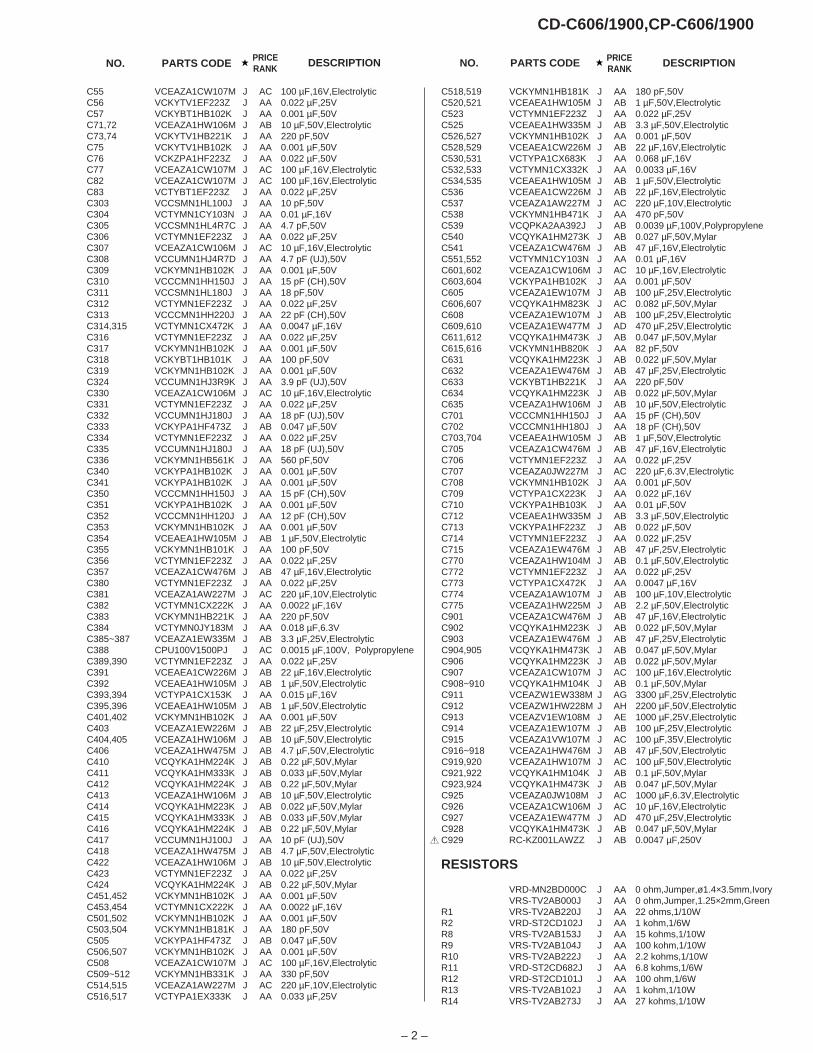
NO. PRICERANK DESCRIPTIONPARTS CODENO. PARTS CODE PRICE
RANK DESCRIPTION
CD-C606/1900,CP-C606/1900
– 2 –
C55 VCEAZA1CW107M J AC 100 µF,16V,ElectrolyticC56 VCKYTV1EF223Z J AA 0.022 µF,25VC57 VCKYBT1HB102K J AA 0.001 µF,50VC71,72 VCEAZA1HW106M J AB 10 µF,50V,ElectrolyticC73,74 VCKYTV1HB221K J AA 220 pF,50VC75 VCKYTV1HB102K J AA 0.001 µF,50VC76 VCKZPA1HF223Z J AA 0.022 µF,50VC77 VCEAZA1CW107M J AC 100 µF,16V,ElectrolyticC82 VCEAZA1CW107M J AC 100 µF,16V,ElectrolyticC83 VCTYBT1EF223Z J AA 0.022 µF,25VC303 VCCSMN1HL100J J AA 10 pF,50VC304 VCTYMN1CY103N J AA 0.01 µF,16VC305 VCCSMN1HL4R7C J AA 4.7 pF,50VC306 VCTYMN1EF223Z J AA 0.022 µF,25VC307 VCEAZA1CW106M J AC 10 µF,16V,ElectrolyticC308 VCCUMN1HJ4R7D J AA 4.7 pF (UJ),50VC309 VCKYMN1HB102K J AA 0.001 µF,50VC310 VCCCMN1HH150J J AA 15 pF (CH),50VC311 VCCSMN1HL180J J AA 18 pF,50VC312 VCTYMN1EF223Z J AA 0.022 µF,25VC313 VCCCMN1HH220J J AA 22 pF (CH),50VC314,315 VCTYMN1CX472K J AA 0.0047 µF,16VC316 VCTYMN1EF223Z J AA 0.022 µF,25VC317 VCKYMN1HB102K J AA 0.001 µF,50VC318 VCKYBT1HB101K J AA 100 pF,50VC319 VCKYMN1HB102K J AA 0.001 µF,50VC324 VCCUMN1HJ3R9K J AA 3.9 pF (UJ),50VC330 VCEAZA1CW106M J AC 10 µF,16V,ElectrolyticC331 VCTYMN1EF223Z J AA 0.022 µF,25VC332 VCCUMN1HJ180J J AA 18 pF (UJ),50VC333 VCKYPA1HF473Z J AB 0.047 µF,50VC334 VCTYMN1EF223Z J AA 0.022 µF,25VC335 VCCUMN1HJ180J J AA 18 pF (UJ),50VC336 VCKYMN1HB561K J AA 560 pF,50VC340 VCKYPA1HB102K J AA 0.001 µF,50VC341 VCKYPA1HB102K J AA 0.001 µF,50VC350 VCCCMN1HH150J J AA 15 pF (CH),50VC351 VCKYPA1HB102K J AA 0.001 µF,50VC352 VCCCMN1HH120J J AA 12 pF (CH),50VC353 VCKYMN1HB102K J AA 0.001 µF,50VC354 VCEAEA1HW105M J AB 1 µF,50V,ElectrolyticC355 VCKYMN1HB101K J AA 100 pF,50VC356 VCTYMN1EF223Z J AA 0.022 µF,25VC357 VCEAZA1CW476M J AB 47 µF,16V,ElectrolyticC380 VCTYMN1EF223Z J AA 0.022 µF,25VC381 VCEAZA1AW227M J AC 220 µF,10V,ElectrolyticC382 VCTYMN1CX222K J AA 0.0022 µF,16VC383 VCKYMN1HB221K J AA 220 pF,50VC384 VCTYMN0JY183M J AA 0.018 µF,6.3VC385~387 VCEAZA1EW335M J AB 3.3 µF,25V,ElectrolyticC388 CPU100V1500PJ J AC 0.0015 µF,100V, PolypropyleneC389,390 VCTYMN1EF223Z J AA 0.022 µF,25VC391 VCEAEA1CW226M J AB 22 µF,16V,ElectrolyticC392 VCEAEA1HW105M J AB 1 µF,50V,ElectrolyticC393,394 VCTYPA1CX153K J AA 0.015 µF,16VC395,396 VCEAEA1HW105M J AB 1 µF,50V,ElectrolyticC401,402 VCKYMN1HB102K J AA 0.001 µF,50VC403 VCEAZA1EW226M J AB 22 µF,25V,ElectrolyticC404,405 VCEAZA1HW106M J AB 10 µF,50V,ElectrolyticC406 VCEAZA1HW475M J AB 4.7 µF,50V,ElectrolyticC410 VCQYKA1HM224K J AB 0.22 µF,50V,MylarC411 VCQYKA1HM333K J AB 0.033 µF,50V,MylarC412 VCQYKA1HM224K J AB 0.22 µF,50V,MylarC413 VCEAZA1HW106M J AB 10 µF,50V,ElectrolyticC414 VCQYKA1HM223K J AB 0.022 µF,50V,MylarC415 VCQYKA1HM333K J AB 0.033 µF,50V,MylarC416 VCQYKA1HM224K J AB 0.22 µF,50V,MylarC417 VCCUMN1HJ100J J AA 10 pF (UJ),50VC418 VCEAZA1HW475M J AB 4.7 µF,50V,ElectrolyticC422 VCEAZA1HW106M J AB 10 µF,50V,ElectrolyticC423 VCTYMN1EF223Z J AA 0.022 µF,25VC424 VCQYKA1HM224K J AB 0.22 µF,50V,MylarC451,452 VCKYMN1HB102K J AA 0.001 µF,50VC453,454 VCTYMN1CX222K J AA 0.0022 µF,16VC501,502 VCKYMN1HB102K J AA 0.001 µF,50VC503,504 VCKYMN1HB181K J AA 180 pF,50VC505 VCKYPA1HF473Z J AB 0.047 µF,50VC506,507 VCKYMN1HB102K J AA 0.001 µF,50VC508 VCEAZA1CW107M J AC 100 µF,16V,ElectrolyticC509~512 VCKYMN1HB331K J AA 330 pF,50VC514,515 VCEAZA1AW227M J AC 220 µF,10V,ElectrolyticC516,517 VCTYPA1EX333K J AA 0.033 µF,25V
C518,519 VCKYMN1HB181K J AA 180 pF,50VC520,521 VCEAEA1HW105M J AB 1 µF,50V,ElectrolyticC523 VCTYMN1EF223Z J AA 0.022 µF,25VC525 VCEAEA1HW335M J AB 3.3 µF,50V,ElectrolyticC526,527 VCKYMN1HB102K J AA 0.001 µF,50VC528,529 VCEAEA1CW226M J AB 22 µF,16V,ElectrolyticC530,531 VCTYPA1CX683K J AA 0.068 µF,16VC532,533 VCTYMN1CX332K J AA 0.0033 µF,16VC534,535 VCEAEA1HW105M J AB 1 µF,50V,ElectrolyticC536 VCEAEA1CW226M J AB 22 µF,16V,ElectrolyticC537 VCEAZA1AW227M J AC 220 µF,10V,ElectrolyticC538 VCKYMN1HB471K J AA 470 pF,50VC539 VCQPKA2AA392J J AB 0.0039 µF,100V,PolypropyleneC540 VCQYKA1HM273K J AB 0.027 µF,50V,MylarC541 VCEAZA1CW476M J AB 47 µF,16V,ElectrolyticC551,552 VCTYMN1CY103N J AA 0.01 µF,16VC601,602 VCEAZA1CW106M J AC 10 µF,16V,ElectrolyticC603,604 VCKYPA1HB102K J AA 0.001 µF,50VC605 VCEAZA1EW107M J AB 100 µF,25V,ElectrolyticC606,607 VCQYKA1HM823K J AC 0.082 µF,50V,MylarC608 VCEAZA1EW107M J AB 100 µF,25V,ElectrolyticC609,610 VCEAZA1EW477M J AD 470 µF,25V,ElectrolyticC611,612 VCQYKA1HM473K J AB 0.047 µF,50V,MylarC615,616 VCKYMN1HB820K J AA 82 pF,50VC631 VCQYKA1HM223K J AB 0.022 µF,50V,MylarC632 VCEAZA1EW476M J AB 47 µF,25V,ElectrolyticC633 VCKYBT1HB221K J AA 220 pF,50VC634 VCQYKA1HM223K J AB 0.022 µF,50V,MylarC635 VCEAZA1HW106M J AB 10 µF,50V,ElectrolyticC701 VCCCMN1HH150J J AA 15 pF (CH),50VC702 VCCCMN1HH180J J AA 18 pF (CH),50VC703,704 VCEAEA1HW105M J AB 1 µF,50V,ElectrolyticC705 VCEAZA1CW476M J AB 47 µF,16V,ElectrolyticC706 VCTYMN1EF223Z J AA 0.022 µF,25VC707 VCEAZA0JW227M J AC 220 µF,6.3V,ElectrolyticC708 VCKYMN1HB102K J AA 0.001 µF,50VC709 VCTYPA1CX223K J AA 0.022 µF,16VC710 VCKYPA1HB103K J AA 0.01 µF,50VC712 VCEAEA1HW335M J AB 3.3 µF,50V,ElectrolyticC713 VCKYPA1HF223Z J AB 0.022 µF,50VC714 VCTYMN1EF223Z J AA 0.022 µF,25VC715 VCEAZA1EW476M J AB 47 µF,25V,ElectrolyticC770 VCEAZA1HW104M J AB 0.1 µF,50V,ElectrolyticC772 VCTYMN1EF223Z J AA 0.022 µF,25VC773 VCTYPA1CX472K J AA 0.0047 µF,16VC774 VCEAZA1AW107M J AB 100 µF,10V,ElectrolyticC775 VCEAZA1HW225M J AB 2.2 µF,50V,ElectrolyticC901 VCEAZA1CW476M J AB 47 µF,16V,ElectrolyticC902 VCQYKA1HM223K J AB 0.022 µF,50V,MylarC903 VCEAZA1EW476M J AB 47 µF,25V,ElectrolyticC904,905 VCQYKA1HM473K J AB 0.047 µF,50V,MylarC906 VCQYKA1HM223K J AB 0.022 µF,50V,MylarC907 VCEAZA1CW107M J AC 100 µF,16V,ElectrolyticC908~910 VCQYKA1HM104K J AB 0.1 µF,50V,MylarC911 VCEAZW1EW338M J AG 3300 µF,25V,ElectrolyticC912 VCEAZW1HW228M J AH 2200 µF,50V,ElectrolyticC913 VCEAZV1EW108M J AE 1000 µF,25V,ElectrolyticC914 VCEAZA1EW107M J AB 100 µF,25V,ElectrolyticC915 VCEAZA1VW107M J AC 100 µF,35V,ElectrolyticC916~918 VCEAZA1HW476M J AB 47 µF,50V,ElectrolyticC919,920 VCEAZA1HW107M J AC 100 µF,50V,ElectrolyticC921,922 VCQYKA1HM104K J AB 0.1 µF,50V,MylarC923,924 VCQYKA1HM473K J AB 0.047 µF,50V,MylarC925 VCEAZA0JW108M J AC 1000 µF,6.3V,ElectrolyticC926 VCEAZA1CW106M J AC 10 µF,16V,ElectrolyticC927 VCEAZA1EW477M J AD 470 µF,25V,ElectrolyticC928 VCQYKA1HM473K J AB 0.047 µF,50V,Mylar
! C929 RC-KZ001LAWZZ J AB 0.0047 µF,250V
RESISTORS
VRD-MN2BD000C J AA 0 ohm,Jumper,ø1.4×3.5mm,IvoryVRS-TV2AB000J J AA 0 ohm,Jumper,1.25×2mm,Green
R1 VRS-TV2AB220J J AA 22 ohms,1/10WR2 VRD-ST2CD102J J AA 1 kohm,1/6WR8 VRS-TV2AB153J J AA 15 kohms,1/10WR9 VRS-TV2AB104J J AA 100 kohm,1/10WR10 VRS-TV2AB222J J AA 2.2 kohms,1/10WR11 VRD-ST2CD682J J AA 6.8 kohms,1/6WR12 VRD-ST2CD101J J AA 100 ohm,1/6WR13 VRS-TV2AB102J J AA 1 kohm,1/10WR14 VRS-TV2AB273J J AA 27 kohms,1/10W
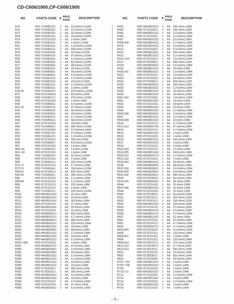
PRICERANK
DESCRIPTIONNO. PARTS CODE NO. PARTS CODE PRICERANK DESCRIPTION
CD-C606/1900,CP-C606/1900
– 3 –
R15 VRS-TV2AB123J J AA 12 kohms,1/10WR16 VRS-TV2AB332J J AA 3.3 kohms,1/10WR17 VRS-TV2AB333J J AA 33 kohms,1/10WR18 VRS-TV2AB153J J AA 15 kohms,1/10WR19 VRD-ST2CD102J J AA 1 kohm,1/6WR20 VRS-TV2AB102J J AA 1 kohm,1/10WR21 VRS-TV2AB152J J AA 1.5 kohms,1/10WR22 VRS-TV2AB821J J AA 820 ohms,1/10WR23 VRS-TV2AB103J J AA 10 kohm,1/10WR24 VRS-TV2AB473J J AA 47 kohms,1/10WR25 VRS-TV2AB152J J AA 1.5 kohms,1/10WR26 VRS-TV2AB823J J AA 82 kohms,1/10WR27 VRS-TV2AB393J J AA 39 kohms,1/10WR28 VRS-TV2AB103J J AA 10 kohm,1/10WR29 VRS-TV2AB563J J AA 56 kohms,1/10WR30 VRS-TV2AB682J J AA 6.8 kohms,1/10WR31 VRS-TV2AB122J J AA 1.2 kohms,1/10WR32 VRS-TV2AB103J J AA 10 kohm,1/10WR33 VRS-TV2AB122J J AA 1.2 kohms,1/10WR34 VRS-TV2AB102J J AA 1 kohm,1/10WR35,36 VRS-TV2AB224J J AA 220 kohms,1/10WR37 VRD-ST2CD823J J AA 82 kohms,1/6WR38 VRS-TV2AB471J J AA 470 ohms,1/10WR39 VRD-ST2CD102J J AA 1 kohm,1/6WR40 VRS-TV2AB562J J AA 5.6 kohms,1/10WR41,42 VRS-TV2AB473J J AA 47 kohms,1/10WR43 VRS-TV2AB563J J AA 56 kohms,1/10WR44 VRS-TV2AB333J J AA 33 kohms,1/10WR45 VRS-TV2AB472J J AA 4.7 kohms,1/10WR46 VRS-TV2AB561J J AA 560 ohms,1/10WR47 VRD-ST2CD103J J AA 10 kohm,1/6WR50 VRS-TV2AB681J J AA 680 ohms,1/10WR51 VRD-ST2CD335J J AA 3.3 Mohms,1/6WR52 VRS-TV2AB273J J AA 27 kohms,1/10WR53 VRS-TV2AB122J J AA 1.2 kohms,1/10WR55 VRD-ST2CD101J J AA 100 ohm,1/6WR56 VRS-TV2AB682J J AA 6.8 kohms,1/10WR57 VRD-ST2CD102J J AA 1 kohm,1/6WR58~60 VRS-TV2AB102J J AA 1 kohm,1/10WR61~63 VRD-ST2CD102J J AA 1 kohm,1/6WR64 VRS-TV2AB220J J AA 22 ohms,1/10WR65 VRD-ST2CD102J J AA 1 kohm,1/6WR66 VRS-TV2AB221J J AA 220 ohms,1/10WR71,72 VRD-ST2CD272J J AA 2.7 kohms,1/6WR73,74 VRS-TV2AB104J J AA 100 kohm,1/10WR80,81 VRD-ST2CD821J J AA 820 ohms,1/6WR82,83 VRS-TV2AB391J J AA 390 ohms,1/10WR84 VRD-ST2CD222J J AA 2.2 kohms,1/6WR88,89 VRD-ST2CD122J J AA 1.2 kohms,1/6WR90 VRD-ST2CD221J J AA 220 ohms,1/6WR91 VRD-ST2CD102J J AA 1 kohm,1/6WR93 VRS-TV2AB221J J AA 220 ohms,1/10WR301 VRD-MN2BD100J J AA 10 ohm,1/8WR309 VRD-MN2BD103J J AA 10 kohm,1/8WR311 VRD-MN2BD104J J AA 100 kohm,1/8WR312 VRD-ST2CD470J J AA 47 ohms,1/6WR313 VRD-MN2BD333J J AA 33 kohms,1/8WR314 VRD-ST2CD220J J AA 22 ohms,1/6WR315 VRD-MN2BD821J J AA 820 ohms,1/8WR317 VRD-MN2BD472J J AA 4.7 kohms,1/8WR322 VRD-MN2BD681J J AA 680 ohms,1/8WR323 VRD-MN2BD224J J AA 220 kohms,1/8WR341 VRD-MN2BD103J J AA 10 kohm,1/8WR343 VRD-MN2BD683J J AA 68 kohms,1/8WR351 VRD-MN2BD152J J AA 1.5 kohms,1/8WR352 VRD-MN2BD103J J AA 10 kohm,1/8WR353 VRD-MN2BD222J J AA 2.2 kohms,1/8WR354~358 VRD-ST2CD102J J AA 1 kohm,1/6WR361 VRD-MN2BD473J J AA 47 kohms,1/8WR380 VRD-MN2BD392J J AA 3.9 kohms,1/8WR381 VRD-MN2BD333J J AA 33 kohms,1/8WR382 VRD-MN2BD152J J AA 1.5 kohms,1/8WR383 VRD-MN2BD122J J AA 1.2 kohms,1/8WR384 VRD-MN2BD153J J AA 15 kohms,1/8WR385 VRD-MN2BD103J J AA 10 kohm,1/8WR386 VRD-ST2EE391J J AA 390 ohms,1/4WR387 VRD-ST2EE331J J AA 330 ohms,1/4WR388 VRD-MN2BD332J J AA 3.3 kohms,1/8WR389 VRD-MN2BD103J J AA 10 kohm,1/8WR390 VRD-ST2CD222J J AA 2.2 kohms,1/6WR391 VRD-ST2CD470J J AA 47 ohms,1/6WR398 VRD-MN2BD562J J AA 5.6 kohms,1/8W
R401 VRD-MN2BD331J J AA 330 ohms,1/8WR402 VRD-ST2CD331J J AA 330 ohms,1/6WR405 VRD-MN2BD222J J AA 2.2 kohms,1/8WR406 VRD-ST2CD222J J AA 2.2 kohms,1/6WR407 VRD-MN2BD223J J AA 22 kohms,1/8WR408,409 VRD-MN2BD472J J AA 4.7 kohms,1/8WR410 VRD-MN2BD332J J AA 3.3 kohms,1/8WR411 VRD-ST2CD332J J AA 3.3 kohms,1/6WR412 VRD-MN2BD331J J AA 330 ohms,1/8WR413 VRD-MN2BD222J J AA 2.2 kohms,1/8WR414~416 VRD-ST2CD152J J AA 1.5 kohms,1/6WR417 VRD-RT2HD561J J AA 560 ohms,1/2WR418 VRD-MN2BD562J J AA 5.6 kohms,1/8WR419 VRD-MN2BD103J J AA 10 kohm,1/8WR420,421 VRD-MN2BD152J J AA 1.5 kohms,1/8WR422 VRD-ST2CD152J J AA 1.5 kohms,1/6WR423 VRD-ST2CD223J J AA 22 kohms,1/6WR424 VRD-RT2HD821J J AA 820 ohms,1/2WR425 VRD-MN2BD331J J AA 330 ohms,1/8WR426 VRD-MN2BD222J J AA 2.2 kohms,1/8WR428 VRD-MN2BD153J J AA 15 kohms,1/8WR430 VRD-MN2BD153J J AA 15 kohms,1/8WR451,452 VRD-ST2CD182J J AA 1.8 kohms,1/6WR501 VRD-MN2BD103J J AA 10 kohm,1/8WR502 VRD-ST2CD103J J AA 10 kohm,1/6WR503 VRD-MN2BD103J J AA 10 kohm,1/8WR504 VRD-MN2BD222J J AA 2.2 kohms,1/8WR505,506 VRD-MN2BD332J J AA 3.3 kohms,1/8WR507 VRD-MN2BD222J J AA 2.2 kohms,1/8WR508,509 VRD-MN2BD103J J AA 10 kohm,1/8WR510 VRD-ST2CD472J J AA 4.7 kohms,1/6WR511,512 VRD-MN2BD473J J AA 47 kohms,1/8WR513 VRD-ST2CD472J J AA 4.7 kohms,1/6WR514 VRD-MN2BD102J J AA 1 kohm,1/8WR515 VRD-ST2CD102J J AA 1 kohm,1/6WR516 VRD-MN2BD151J J AA 150 ohms,1/8WR517 VRD-MN2BD102J J AA 1 kohm,1/8WR518 VRD-ST2CD102J J AA 1 kohm,1/6WR522,523 VRD-ST2CD270J J AA 27 ohms,1/6WR524,525 VRD-MN2BD104J J AA 100 kohm,1/8WR526,527 VRD-MN2BD472J J AA 4.7 kohms,1/8WR531,532 VRD-ST2CD102J J AA 1 kohm,1/6WR533,534 VRD-MN2BD333J J AA 33 kohms,1/8WR536 VRD-MN2BD683J J AA 68 kohms,1/8WR537,538 VRD-MN2BD562J J AA 5.6 kohms,1/8WR539,540 VRD-MN2BD682J J AA 6.8 kohms,1/8WR541,542 VRD-MN2BD561J J AA 560 ohms,1/8WR543 VRD-ST2CD823J J AA 82 kohms,1/6WR544,545 VRD-MN2BD560J J AA 56 ohms,1/8WR546 VRD-ST2CD103J J AA 10 kohm,1/6WR547,548 VRD-MN2BD103J J AA 10 kohm,1/8WR549 VRD-ST2CD103J J AA 10 kohm,1/6WR550 VRD-ST2CD823J J AA 82 kohms,1/6WR551 VRD-ST2EE221J J AA 220 ohms,1/4WR552 VRD-RT2HD151J J AA 150 ohms,1/2WR553 VRD-MN2BD104J J AA 100 kohm,1/8WR554 VRD-ST2CD473J J AA 47 kohms,1/6WR555 VRD-MN2BD473J J AA 47 kohms,1/8WR556 VRD-MN2BD472J J AA 4.7 kohms,1/8WR557 VRD-MN2BD120J J AA 12 ohms,1/8WR561 VRD-ST2CD223J J AA 22 kohms,1/6WR601 VRD-ST2CD472J J AA 4.7 kohms,1/6WR602 VRD-MN2BD472J J AA 4.7 kohms,1/8WR603,604 VRD-ST2CD332J J AA 3.3 kohms,1/6WR605 VRD-ST2CD121J J AA 120 ohms,1/6WR606,607 VRD-ST2CD102J J AA 1 kohm,1/6WR608 VRD-ST2CD121J J AA 120 ohms,1/6WR609,610 VRD-RT2HD271J J AA 270 ohms,1/2WR611,612 VRD-ST2EE4R7J J AA 4.7 ohms,1/4WR613,614 VRD-ST2EE331J J AA 330 ohms,1/4WR631 VRD-ST2CD223J J AA 22 kohms,1/6WR632 VRD-ST2EE821J J AA 820 ohms,1/4WR633 VRD-ST2CD563J J AA 56 kohms,1/6WR701~703 VRD-MN2BD102J J AA 1 kohm,1/8WR704~708 VRD-MN2BD102J J AA 1 kohm,1/8WR709 VRD-ST2CD102J J AA 1 kohm,1/6WR710,711 VRD-MN2BD102J J AA 1 kohm,1/8WR712 VRD-ST2CD222J J AA 2.2 kohms,1/6WR713 VRD-MN2BD102J J AA 1 kohm,1/8WR714 VRD-ST2CD222J J AA 2.2 kohms,1/6WR715 VRD-MN2BD102J J AA 1 kohm,1/8WR716 VRD-ST2CD102J J AA 1 kohm,1/6W
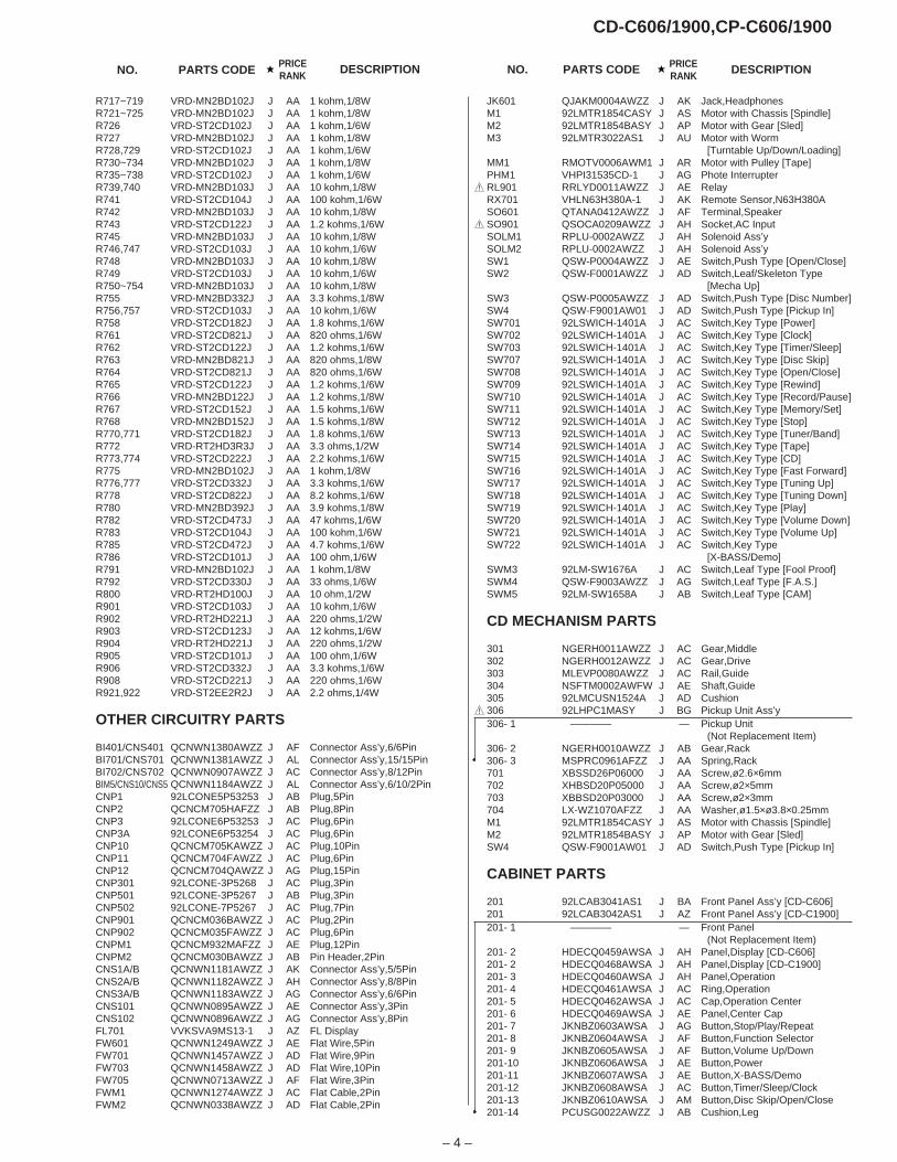
NO. PRICERANK DESCRIPTIONPARTS CODENO. PARTS CODE PRICE
RANK DESCRIPTION
CD-C606/1900,CP-C606/1900
– 4 –
R717~719 VRD-MN2BD102J J AA 1 kohm,1/8WR721~725 VRD-MN2BD102J J AA 1 kohm,1/8WR726 VRD-ST2CD102J J AA 1 kohm,1/6WR727 VRD-MN2BD102J J AA 1 kohm,1/8WR728,729 VRD-ST2CD102J J AA 1 kohm,1/6WR730~734 VRD-MN2BD102J J AA 1 kohm,1/8WR735~738 VRD-ST2CD102J J AA 1 kohm,1/6WR739,740 VRD-MN2BD103J J AA 10 kohm,1/8WR741 VRD-ST2CD104J J AA 100 kohm,1/6WR742 VRD-MN2BD103J J AA 10 kohm,1/8WR743 VRD-ST2CD122J J AA 1.2 kohms,1/6WR745 VRD-MN2BD103J J AA 10 kohm,1/8WR746,747 VRD-ST2CD103J J AA 10 kohm,1/6WR748 VRD-MN2BD103J J AA 10 kohm,1/8WR749 VRD-ST2CD103J J AA 10 kohm,1/6WR750~754 VRD-MN2BD103J J AA 10 kohm,1/8WR755 VRD-MN2BD332J J AA 3.3 kohms,1/8WR756,757 VRD-ST2CD103J J AA 10 kohm,1/6WR758 VRD-ST2CD182J J AA 1.8 kohms,1/6WR761 VRD-ST2CD821J J AA 820 ohms,1/6WR762 VRD-ST2CD122J J AA 1.2 kohms,1/6WR763 VRD-MN2BD821J J AA 820 ohms,1/8WR764 VRD-ST2CD821J J AA 820 ohms,1/6WR765 VRD-ST2CD122J J AA 1.2 kohms,1/6WR766 VRD-MN2BD122J J AA 1.2 kohms,1/8WR767 VRD-ST2CD152J J AA 1.5 kohms,1/6WR768 VRD-MN2BD152J J AA 1.5 kohms,1/8WR770,771 VRD-ST2CD182J J AA 1.8 kohms,1/6WR772 VRD-RT2HD3R3J J AA 3.3 ohms,1/2WR773,774 VRD-ST2CD222J J AA 2.2 kohms,1/6WR775 VRD-MN2BD102J J AA 1 kohm,1/8WR776,777 VRD-ST2CD332J J AA 3.3 kohms,1/6WR778 VRD-ST2CD822J J AA 8.2 kohms,1/6WR780 VRD-MN2BD392J J AA 3.9 kohms,1/8WR782 VRD-ST2CD473J J AA 47 kohms,1/6WR783 VRD-ST2CD104J J AA 100 kohm,1/6WR785 VRD-ST2CD472J J AA 4.7 kohms,1/6WR786 VRD-ST2CD101J J AA 100 ohm,1/6WR791 VRD-MN2BD102J J AA 1 kohm,1/8WR792 VRD-ST2CD330J J AA 33 ohms,1/6WR800 VRD-RT2HD100J J AA 10 ohm,1/2WR901 VRD-ST2CD103J J AA 10 kohm,1/6WR902 VRD-RT2HD221J J AA 220 ohms,1/2WR903 VRD-ST2CD123J J AA 12 kohms,1/6WR904 VRD-RT2HD221J J AA 220 ohms,1/2WR905 VRD-ST2CD101J J AA 100 ohm,1/6WR906 VRD-ST2CD332J J AA 3.3 kohms,1/6WR908 VRD-ST2CD221J J AA 220 ohms,1/6WR921,922 VRD-ST2EE2R2J J AA 2.2 ohms,1/4W
OTHER CIRCUITRY PARTS
BI401/CNS401 QCNWN1380AWZZ J AF Connector Ass’y,6/6PinBI701/CNS701 QCNWN1381AWZZ J AL Connector Ass’y,15/15PinBI702/CNS702 QCNWN0907AWZZ J AC Connector Ass’y,8/12PinBIM5/CNS10/CNS5 QCNWN1184AWZZ J AL Connector Ass’y,6/10/2PinCNP1 92LCONE5P53253 J AB Plug,5PinCNP2 QCNCM705HAFZZ J AB Plug,8PinCNP3 92LCONE6P53253 J AC Plug,6PinCNP3A 92LCONE6P53254 J AC Plug,6PinCNP10 QCNCM705KAWZZ J AC Plug,10PinCNP11 QCNCM704FAWZZ J AC Plug,6PinCNP12 QCNCM704QAWZZ J AG Plug,15PinCNP301 92LCONE-3P5268 J AC Plug,3PinCNP501 92LCONE-3P5267 J AB Plug,3PinCNP502 92LCONE-7P5267 J AC Plug,7PinCNP901 QCNCM036BAWZZ J AC Plug,2PinCNP902 QCNCM035FAWZZ J AC Plug,6PinCNPM1 QCNCM932MAFZZ J AE Plug,12PinCNPM2 QCNCM030BAWZZ J AB Pin Header,2PinCNS1A/B QCNWN1181AWZZ J AK Connector Ass’y,5/5PinCNS2A/B QCNWN1182AWZZ J AH Connector Ass’y,8/8PinCNS3A/B QCNWN1183AWZZ J AG Connector Ass’y,6/6PinCNS101 QCNWN0895AWZZ J AE Connector Ass’y,3PinCNS102 QCNWN0896AWZZ J AG Connector Ass’y,8PinFL701 VVKSVA9MS13-1 J AZ FL DisplayFW601 QCNWN1249AWZZ J AE Flat Wire,5PinFW701 QCNWN1457AWZZ J AD Flat Wire,9PinFW703 QCNWN1458AWZZ J AD Flat Wire,10PinFW705 QCNWN0713AWZZ J AF Flat Wire,3PinFWM1 QCNWN1274AWZZ J AC Flat Cable,2PinFWM2 QCNWN0338AWZZ J AD Flat Cable,2Pin
JK601 QJAKM0004AWZZ J AK Jack,HeadphonesM1 92LMTR1854CASY J AS Motor with Chassis [Spindle]M2 92LMTR1854BASY J AP Motor with Gear [Sled]M3 92LMTR3022AS1 J AU Motor with Worm
[Turntable Up/Down/Loading]MM1 RMOTV0006AWM1 J AR Motor with Pulley [Tape]PHM1 VHPI31535CD-1 J AG Phote Interrupter
! RL901 RRLYD0011AWZZ J AE RelayRX701 VHLN63H380A-1 J AK Remote Sensor,N63H380ASO601 QTANA0412AWZZ J AF Terminal,Speaker
! SO901 QSOCA0209AWZZ J AH Socket,AC InputSOLM1 RPLU-0002AWZZ J AH Solenoid Ass’ySOLM2 RPLU-0002AWZZ J AH Solenoid Ass’ySW1 QSW-P0004AWZZ J AE Switch,Push Type [Open/Close]SW2 QSW-F0001AWZZ J AD Switch,Leaf/Skeleton Type
[Mecha Up]SW3 QSW-P0005AWZZ J AD Switch,Push Type [Disc Number]SW4 QSW-F9001AW01 J AD Switch,Push Type [Pickup In]SW701 92LSWICH-1401A J AC Switch,Key Type [Power]SW702 92LSWICH-1401A J AC Switch,Key Type [Clock]SW703 92LSWICH-1401A J AC Switch,Key Type [Timer/Sleep]SW707 92LSWICH-1401A J AC Switch,Key Type [Disc Skip]SW708 92LSWICH-1401A J AC Switch,Key Type [Open/Close]SW709 92LSWICH-1401A J AC Switch,Key Type [Rewind]SW710 92LSWICH-1401A J AC Switch,Key Type [Record/Pause]SW711 92LSWICH-1401A J AC Switch,Key Type [Memory/Set]SW712 92LSWICH-1401A J AC Switch,Key Type [Stop]SW713 92LSWICH-1401A J AC Switch,Key Type [Tuner/Band]SW714 92LSWICH-1401A J AC Switch,Key Type [Tape]SW715 92LSWICH-1401A J AC Switch,Key Type [CD]SW716 92LSWICH-1401A J AC Switch,Key Type [Fast Forward]SW717 92LSWICH-1401A J AC Switch,Key Type [Tuning Up]SW718 92LSWICH-1401A J AC Switch,Key Type [Tuning Down]SW719 92LSWICH-1401A J AC Switch,Key Type [Play]SW720 92LSWICH-1401A J AC Switch,Key Type [Volume Down]SW721 92LSWICH-1401A J AC Switch,Key Type [Volume Up]SW722 92LSWICH-1401A J AC Switch,Key Type
[X-BASS/Demo]SWM3 92LM-SW1676A J AC Switch,Leaf Type [Fool Proof]SWM4 QSW-F9003AWZZ J AG Switch,Leaf Type [F.A.S.]SWM5 92LM-SW1658A J AB Switch,Leaf Type [CAM]
CD MECHANISM PARTS
301 NGERH0011AWZZ J AC Gear,Middle302 NGERH0012AWZZ J AC Gear,Drive303 MLEVP0080AWZZ J AC Rail,Guide304 NSFTM0002AWFW J AE Shaft,Guide305 92LMCUSN1524A J AD Cushion
! 306 92LHPC1MASY J BG Pickup Unit Ass’y306- 1 ———— — Pickup Unit
(Not Replacement Item)306- 2 NGERH0010AWZZ J AB Gear,Rack306- 3 MSPRC0961AFZZ J AA Spring,Rack701 XBSSD26P06000 J AA Screw,ø2.6×6mm702 XHBSD20P05000 J AA Screw,ø2×5mm703 XBBSD20P03000 J AA Screw,ø2×3mm704 LX-WZ1070AFZZ J AA Washer,ø1.5×ø3.8×0.25mmM1 92LMTR1854CASY J AS Motor with Chassis [Spindle]M2 92LMTR1854BASY J AP Motor with Gear [Sled]SW4 QSW-F9001AW01 J AD Switch,Push Type [Pickup In]
CABINET PARTS
201 92LCAB3041AS1 J BA Front Panel Ass’y [CD-C606]201 92LCAB3042AS1 J AZ Front Panel Ass’y [CD-C1900]201- 1 ———— — Front Panel
(Not Replacement Item)201- 2 HDECQ0459AWSA J AH Panel,Display [CD-C606]201- 2 HDECQ0468AWSA J AH Panel,Display [CD-C1900]201- 3 HDECQ0460AWSA J AH Panel,Operation201- 4 HDECQ0461AWSA J AC Ring,Operation201- 5 HDECQ0462AWSA J AC Cap,Operation Center201- 6 HDECQ0469AWSA J AE Panel,Center Cap201- 7 JKNBZ0603AWSA J AG Button,Stop/Play/Repeat201- 8 JKNBZ0604AWSA J AF Button,Function Selector201- 9 JKNBZ0605AWSA J AF Button,Volume Up/Down201-10 JKNBZ0606AWSA J AE Button,Power201-11 JKNBZ0607AWSA J AE Button,X-BASS/Demo201-12 JKNBZ0608AWSA J AC Button,Timer/Sleep/Clock201-13 JKNBZ0610AWSA J AM Button,Disc Skip/Open/Close201-14 PCUSG0022AWZZ J AB Cushion,Leg
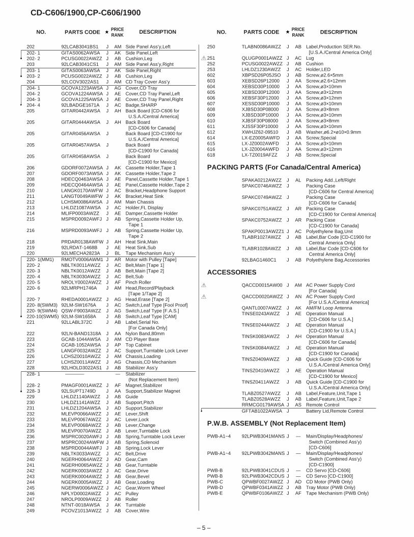
PRICERANK
DESCRIPTIONNO. PARTS CODE NO. PARTS CODE PRICERANK DESCRIPTION
CD-C606/1900,CP-C606/1900
– 5 –
202 92LCAB3041BS1 J AM Side Panel Ass’y,Left202- 1 GITAS0062AWSA J AK Side Panel,Left202- 2 PCUSG0022AWZZ J AB Cushion,Leg203 92LCAB3041CS1 J AM Side Panel Ass’y,Right203- 1 GITAS0063AWSA J AK Side Panel,Right203- 2 PCUSG0022AWZZ J AB Cushion,Leg204 92LCOV3022AS1 J AM CD Tray Cover Ass’y204- 1 GCOVA1223AWSA J AG Cover,CD Tray204- 2 GCOVA1224AWSA J AE Cover,CD Tray Panel,Left204- 3 GCOVA1225AWSA J AE Cover,CD Tray Panel,Right204- 4 92LBADGE1671A J AC Badge,SHARP205 GITAR0442AWSA J AH Back Board [CD-C606 for
U.S.A./Central America]205 GITAR0444AWSA J AH Back Board
[CD-C606 for Canada]205 GITAR0456AWSA J Back Board [CD-C1900 for
U.S.A./Central America]205 GITAR0457AWSA J Back Board
[CD-C1900 for Canada]205 GITAR0458AWSA J Back Board
[CD-C1900 for Mexico]206 GDORF0072AWSA J AK Cassette Holder,Tape 1207 GDORF0073AWSA J AK Cassette Holder,Tape 2208 HDECQ0463AWSA J AE Panel,Cassette Holder,Tape 1209 HDECQ0464AWSA J AE Panel,Cassette Holder,Tape 2210 LANGK0170AWFW J AC Bracket,Headphone Support211 LANGT0049AWFW J AK Bracket,Heat Sink212 LCHSM0086AWSA J AM Main Chassis213 LHLDZ1087AWSA J AC Holder,FL Display214 MLIFP0003AWZZ J AE Damper,Cassette Holder215 MSPRD0092AWFJ J AB Spring,Cassette Holder Up,
Tape 1216 MSPRD0093AWFJ J AB Spring,Cassette Holder Up,
Tape 2218 PRDAR0138AWFW J AH Heat Sink,Main219 92LRDAT-1468B J AE Heat Sink,Sub220 92LMECHA2823A J BL Tape Mechanism Ass’y220- 1(MM1) RMOTV0006AWM1 J AR Motor with Pulley [Tape]220- 2 NBLTK0011AWZZ J AC Belt,Main [Tape 1]220- 3 NBLTK0012AWZZ J AB Belt,Main [Tape 2]220- 4 NBLTK0030AWZZ J AC Belt,Sub220- 5 NROLY0002AWZZ J AF Pinch Roller220- 6 92LMRPH1746A J AM Head,Record/Playback
[Tape 1/Tape 2]220- 7 RHEDA0001AWZZ J AG Head,Erase [Tape 2]220- 8(SWM3) 92LM-SW1676A J AC Switch,Leaf Type [Fool Proof]220- 9(SWM4) QSW-F9003AWZZ J AG Switch,Leaf Type [F.A.S.]220-10(SWM5) 92LM-SW1658A J AB Switch,Leaf Type [CAM]221 92LLABL372C J AB Label,Serial No.
[For Canada Only]222 92LN-BAND1318A J AA Nylon Band,80mm223 GCAB-1044AWSA J AM CD Player Base224 GCAB-1052AWSA J AP Top Cabinet225 LANGF0032AWZZ J AC Support,Turntable Lock Lever226 LCHSZ0010AWZZ J AM Chassis,Loading227 LCHSZ0011AWZZ J AG Chassis,CD Mechanism228 92LHOLD3022AS1 J AB Stabilizer Ass’y228- 1 ———— — Stabilizer
(Not Replacement Item)228- 2 PMAGF0001AWZZ J AF Magnet,Stabilizer228- 3 92LSUPT1749D J AA Support,Stabilizer Magnet229 LHLDZ1140AWZZ J AB Guide230 LHLDZ1141AWZZ J AB Support,Pitch231 LHLDZ1204AWSA J AD Support,Stabilizer232 MLEVP0066AWZZ J AE Lever,Shift233 MLEVP0067AWZZ J AC Lever,Lock234 MLEVP0068AWZZ J AB Lever,Change235 MLEVP0070AWZZ J AB Lever,Turntable Lock236 MSPRC0020AWFJ J AB Spring,Turntable Lock Lever237 MSPRC0024AWFW J AB Spring,Solenoid238 MSPRD0044AWFJ J AB Spring,Lock Lever239 NBLTK0033AWZZ J AC Belt,Drive240 NGERH0064AWZZ J AD Gear,Cam241 NGERH0065AWZZ J AB Gear,Turntable242 NGERK0003AWZZ J AC Gear,Drive243 NGERK0004AWZZ J AB Gear,Bevel244 NGERK0005AWZZ J AB Gear,Loading245 NGERW0006AWZZ J AC Gear,Worm Wheel246 NPLYD0002AWZZ J AC Pulley247 NROLP0009AWZZ J AB Roller248 NTNT-0018AWSA J AK Turntable249 PCOVZ1013AWZZ J AB Cover,Wire
250 TLABN0086AWZZ J AB Label,Production SER.No.[U.S.A./Central America Only]
! 251 QLUGP0001AWZZ J AC Lug252 PCUSG0022AWZZ J AB Cushion253 LHLDZ1230AWZZ J AC Holder,LED602 XBPSD26P05JSO J AB Screw,ø2.6×5mm603 XEBSD26P12000 J AA Screw,ø2.6×12mm604 XEBSD30P10000 J AA Screw,ø3×10mm605 XEBSD30P12000 J AA Screw,ø3×12mm606 XEBSF30P12000 J AA Screw,ø3×12mm607 XESSD30P10000 J AA Screw,ø3×10mm608 XJBSD30P08000 J AA Screw,ø3×8mm609 XJBSD30P10000 J AA Screw,ø3×10mm610 XJBSF30P08000 J AA Screw,ø3×8mm611 XJSSF30P10000 J AA Screw,ø3×10mm612 XWHJZ62-09510 J AB Washer,ø6.2×ø10×0.9mm614 LX-EZ0005AWFD J AA Screw,Special615 LX-JZ0002AWFD J AA Screw,ø3×10mm616 LX-JZ0004AWFD J AA Screw,ø3×12mm618 LX-TZ0019AFZZ J AB Screw,Special
PACKING PARTS (For Canada/Central America)
SPAKA0212AWZZ J AL Packing Add.,Left/RightSPAKC0746AWZZ J Packing Case
[CD-C606 for Central America]SPAKC0749AWZZ J Packing Case
[CD-C606 for Canada]SPAKC0751AWZZ J AR Packing Case
[CD-C1900 for Central America]SPAKC0752AWZZ J AR Packing Case
[CD-C1900 for Canada]SPAKP0013AWZZ1 J AC Polyethylene Bag,UnitTLABR1027AWZZ J AB Label,Bar Code [CD-C1900 for
Central America Only]TLABR1028AWZZ J AB Label,Bar Code [CD-C606 for
Central America Only]92LBAG1460C1 J AB Polyethylene Bag,Accessories
ACCESSORIES
! QACCD0015AW00 J AM AC Power Supply Cord[For Canada]
! QACCD0020AWZZ J AN AC Power Supply Cord[For U.S.A./Central America]
QANTL0007AWZZ J AK AM/FM Loop AntennaTINSE0243AWZZ J AE Operation Manual
[CD-C606 for U.S.A.]TINSE0244AWZZ J AE Operation Manual
[CD-C1900 for U.S.A.]TINSK0083AWZZ J AH Operation Manual
[CD-C606 for Canada]TINSK0084AWZZ J AE Operation Manual
[CD-C1900 for Canada]TINSZ0409AWZZ J AB Quick Guide [CD-C606 for
U.S.A./Central America Only]TINSZ0410AWZZ J AE Operation Manual
[CD-C1900 for Mexico]TINSZ0411AWZZ J AB Quick Guide [CD-C1900 for
U.S.A./Central America Only]TLABZ0527AWZZ J AB Label,Feature,Unit,Tape 1TLABZ0528AWZZ J AB Label,Feature,Unit,Tape 2RRMCG0179AWSA J AS Remote ControlGFTAB1022AWSA J Battery Lid,Remote Control
P.W.B. ASSEMBLY (Not Replacement Item)
PWB-A1~4 92LPWB3041MANS J — Main/Display/Headphones/Switch (Combined Ass’y)[CD-C606]
PWB-A1~4 92LPWB3042MANS J — Main/Display/Headphones/Switch (Combined Ass’y)[CD-C1900]
PWB-B 92LPWB3041CDUS J — CD Servo [CD-C606]PWB-B 92LPWB3042CDUS J — CD Servo [CD-C1900]PWB-C QPWBF0027AWZZ J AD CD Motor (PWB Only)PWB-D QPWBF0341AWZZ J AB Tray Motor (PWB Only)PWB-E QPWBF0106AWZZ J AF Tape Mechanism (PWB Only)
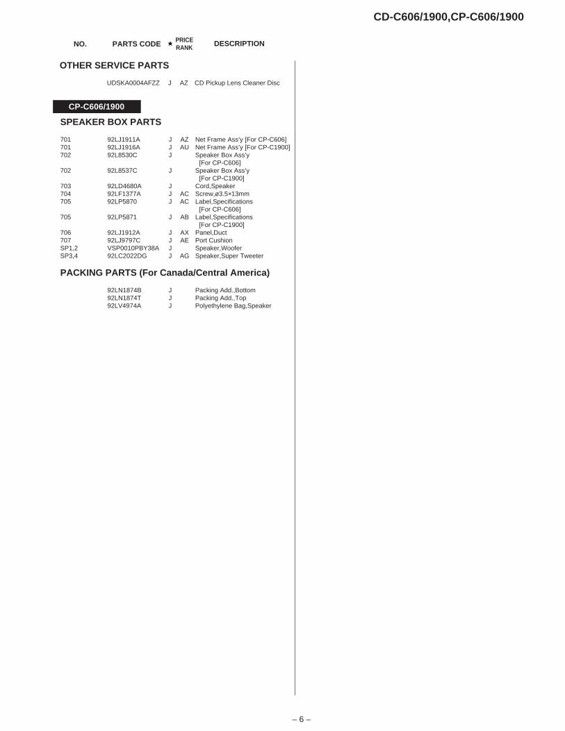
NO. PRICERANK DESCRIPTIONPARTS CODENO. PARTS CODE PRICE
RANK DESCRIPTION
CD-C606/1900,CP-C606/1900
– 6 –
CP-C606/1900
OTHER SERVICE PARTS
UDSKA0004AFZZ J AZ CD Pickup Lens Cleaner Disc
SPEAKER BOX PARTS
701 92LJ1911A J AZ Net Frame Ass’y [For CP-C606]701 92LJ1916A J AU Net Frame Ass’y [For CP-C1900]702 92L8530C J Speaker Box Ass’y
[For CP-C606]702 92L8537C J Speaker Box Ass’y
[For CP-C1900]703 92LD4680A J Cord,Speaker704 92LF1377A J AC Screw,ø3.5×13mm705 92LP5870 J AC Label,Specifications
[For CP-C606]705 92LP5871 J AB Label,Specifications
[For CP-C1900]706 92LJ1912A J AX Panel,Duct707 92LJ9797C J AE Port CushionSP1,2 VSP0010PBY38A J Speaker,WooferSP3,4 92LC2022DG J AG Speaker,Super Tweeter
PACKING PARTS (For Canada/Central America)
92LN1874B J Packing Add.,Bottom92LN1874T J Packing Add.,Top92LV4974A J Polyethylene Bag,Speaker
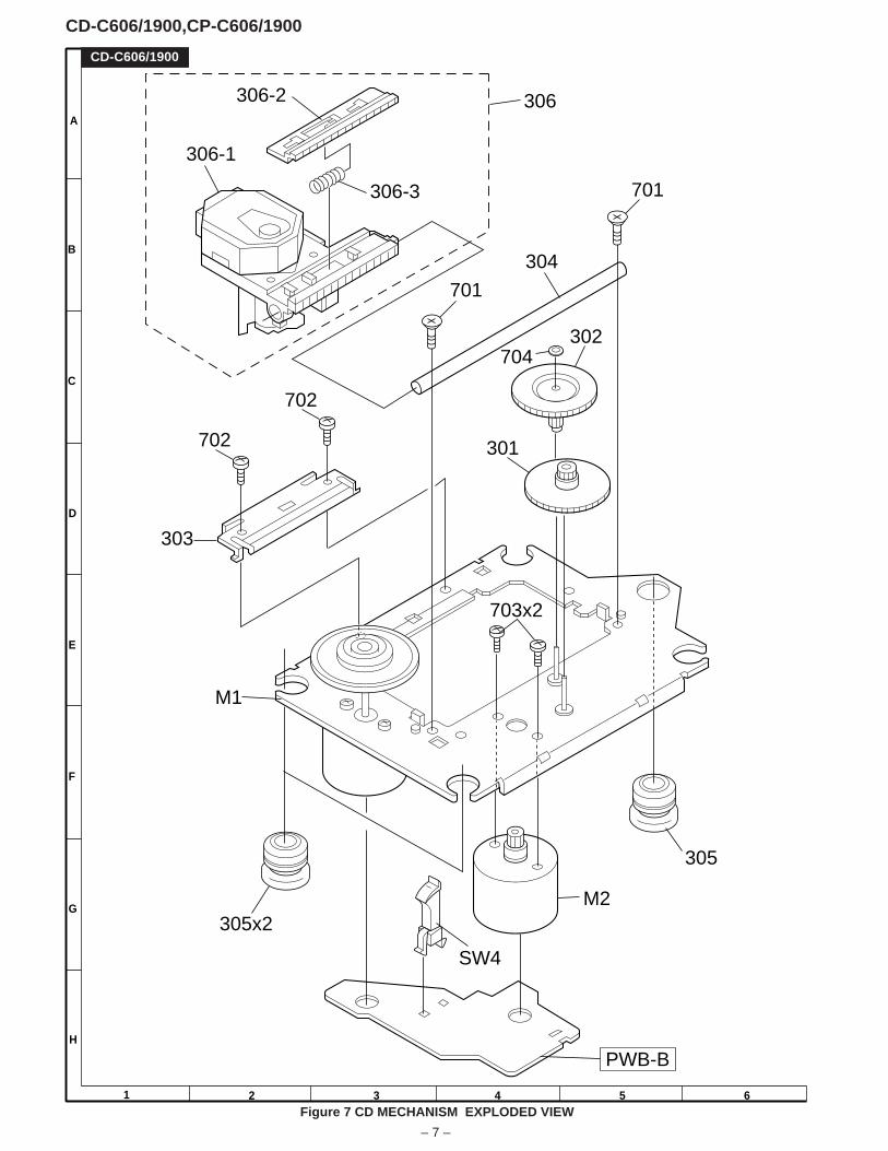
CD-C606/1900,CP-C606/1900
Figure 7 CD MECHANISM EXPLODED VIEW
A
B
C
D
E
F
G
H
1 2 3 4 5 6
– 7 –
CD-C606/1900
306-1
701
304
701
302
301
702
702
303
M1
703x2
305x2
SW4
M2
305
PWB-B
306-2
306-3
306
704
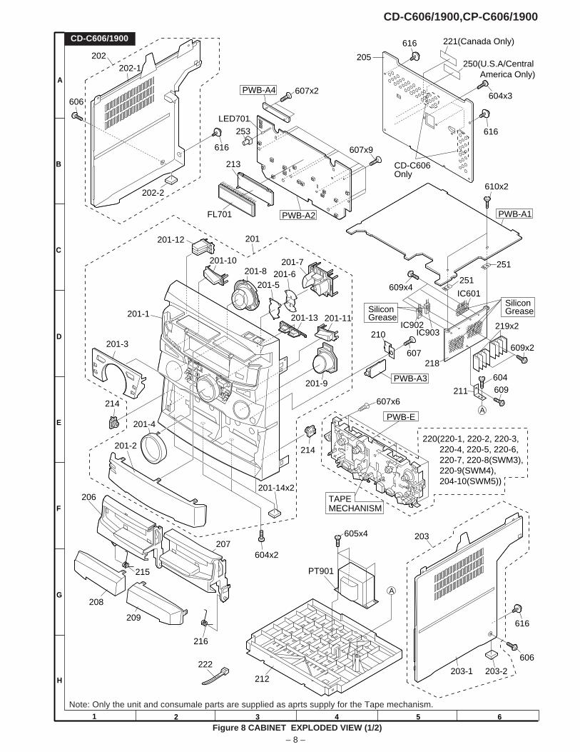
CD-C606/1900,CP-C606/1900
Figure 8 CABINET EXPLODED VIEW (1/2)
A
B
C
D
E
F
G
H
1 2 3 4 5 6
– 8 –
Note: Only the unit and consumale parts are supplied as aprts supply for the Tape mechanism.
CD-C606/1900
PWB-A2
PWB-A3
SiliconGrease
FL701
202
PWB-E
PWB-A4
PWB-A1
607x9
610x2
220(220-1, 220-2, 220-3, 220-4, 220-5, 220-6, 220-7, 220-8(SWM3), 220-9(SWM4), 204-10(SWM5))
SiliconGrease
202-1
202-2
606
616
607x2
213
205
616
616
604x3
221(Canada Only)
250(U.S.A/Central America Only)
609x4
607
210
251
251
IC601
IC903IC902
609604
609x2
219x2
211607x6
214
214A
A
605x4
PT901
212
222203-1 203-2
203
606
616
604x2207
206
215
208
209
216
201-2
201-1
201-4
201-8
201-3
201-12
201-10
201
201-7201-6
201-5
201-13 201-11
201-9
201-14x2TAPEMECHANISM
218
253
LED701
CD-C606Only
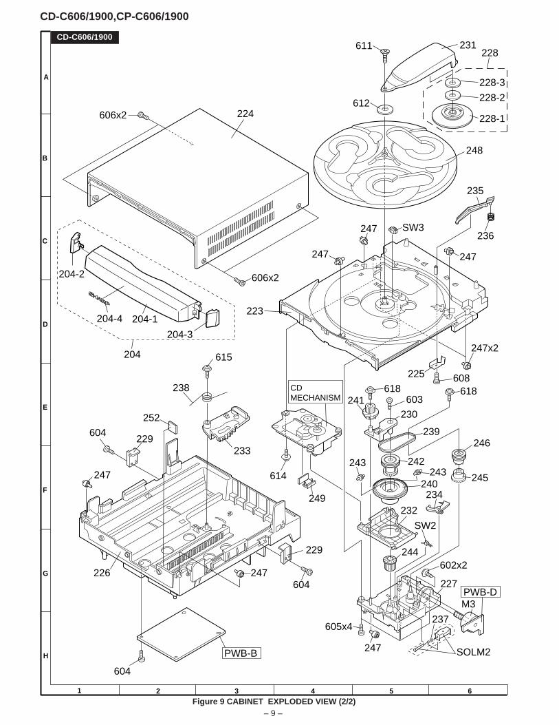
CD-C606/1900,CP-C606/1900
A
B
C
D
E
F
G
H
1 2 3 4 5 6Figure 9 CABINET EXPLODED VIEW (2/2)
– 9 –
CD-C606/1900
CDMECHANISM
604
247
238
615
233
226 247604
229
605x4
247
237
SOLM2
PWB-D
602x2
SW2
234
244
232
240
242
230
603618
241
239
618
246
245
247x2
247
247
247
SW3
223
611 231
248
606x2
606x2
224
204
243243
227
614
249
236
235
228-1
228-2
228-3
228
M3
608225
252
229
PWB-B
604
204-2
204-1
204-3
204-4
612
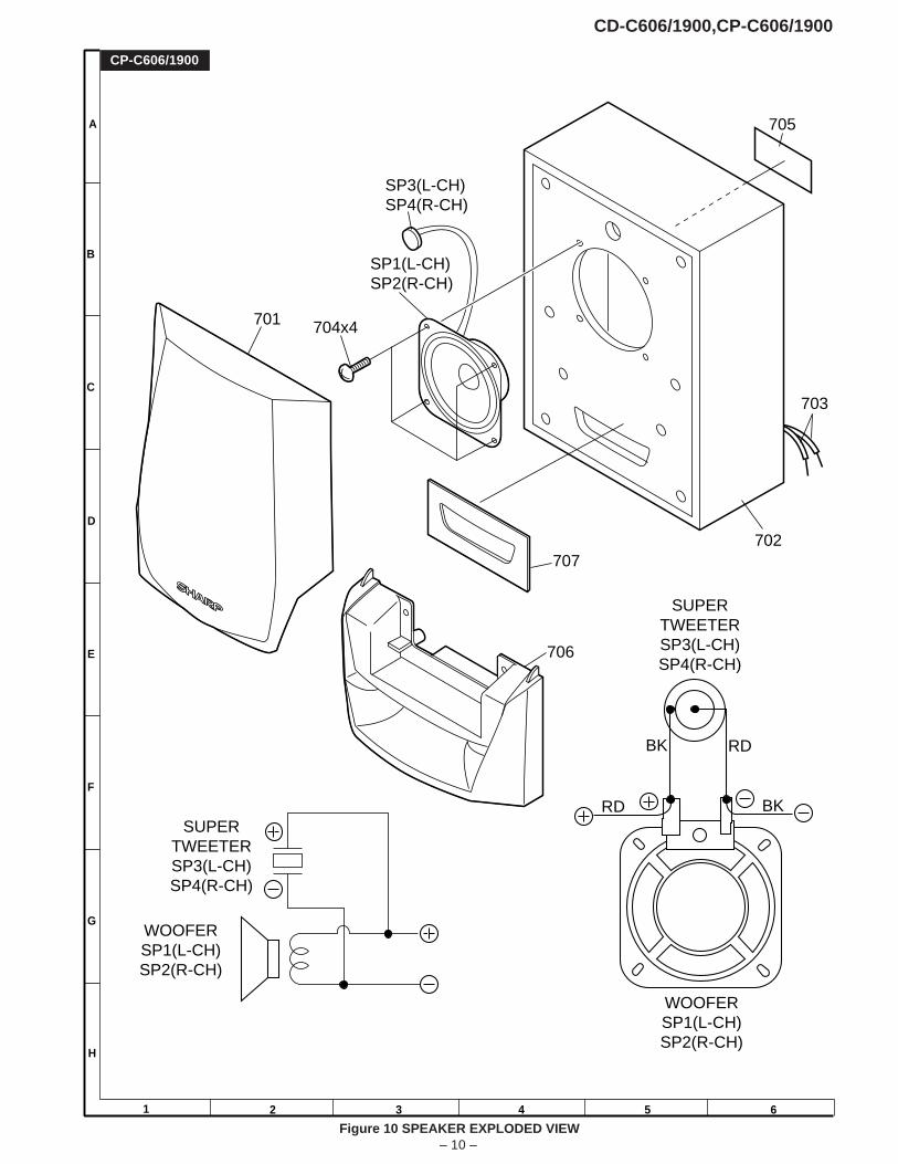
CD-C606/1900,CP-C606/1900
Figure 10 SPEAKER EXPLODED VIEW
A
B
C
D
E
F
G
H
1 2 3 4 5 6
– 10 –
CP-C606/1900
706
704x4
705
703
702707
701
BK
BK
RD
RD
SUPERTWEETERSP3(L-CH)SP4(R-CH)
WOOFERSP1(L-CH)SP2(R-CH)
SUPERTWEETERSP3(L-CH)SP4(R-CH)
WOOFERSP1(L-CH)SP2(R-CH)
SP3(L-CH)SP4(R-CH)
SP1(L-CH)SP2(R-CH)
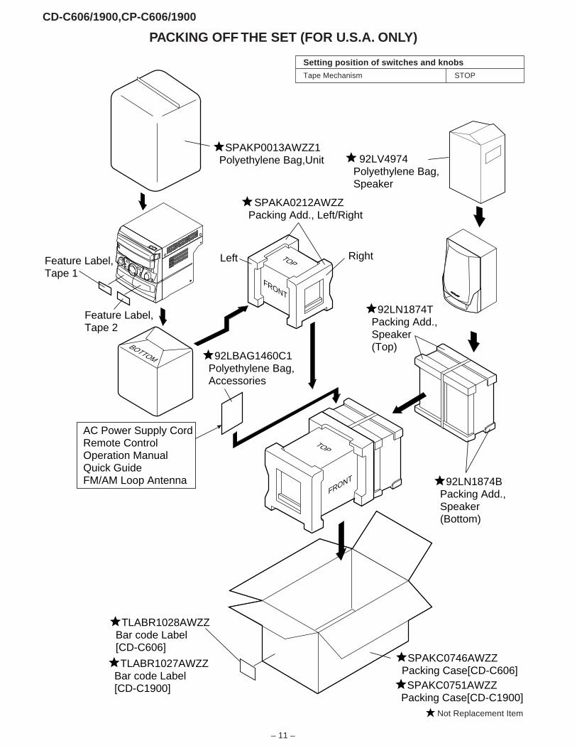
CD-C606/1900,CP-C606/1900
PACKING OFF THE SET (FOR U.S.A. ONLY)
Setting position of switches and knobs
Tape Mechanism STOP
Not Replacement Item
– 11 –
FRONT
TOP
BOTTOM
SPAKP0013AWZZ1Polyethylene Bag,Unit
SPAKA0212AWZZPacking Add., Left/Right
SPAKC0746AWZZPacking Case[CD-C606]
92LBAG1460C1Polyethylene Bag,Accessories
TLABR1028AWZZBar code Label[CD-C606]
92LV4974Polyethylene Bag,Speaker
92LN1874BPacking Add., Speaker(Bottom)
AC Power Supply CordRemote ControlOperation ManualQuick GuideFM/AM Loop Antenna
Left Right
TOP
FRONT
TLABR1027AWZZBar code Label[CD-C1900] SPAKC0751AWZZ
Packing Case[CD-C1900]
Feature Label,Tape 1
Feature Label,Tape 2
92LN1874TPacking Add., Speaker(Top)


![Sharp 19C140 Chasis+CD a[1]](https://img.pdfslide.net/doc/110x75/552167804a795963718b4b8c/sharp-19c140-chasiscd-a1.jpg)