Embed Size (px)
Citation preview
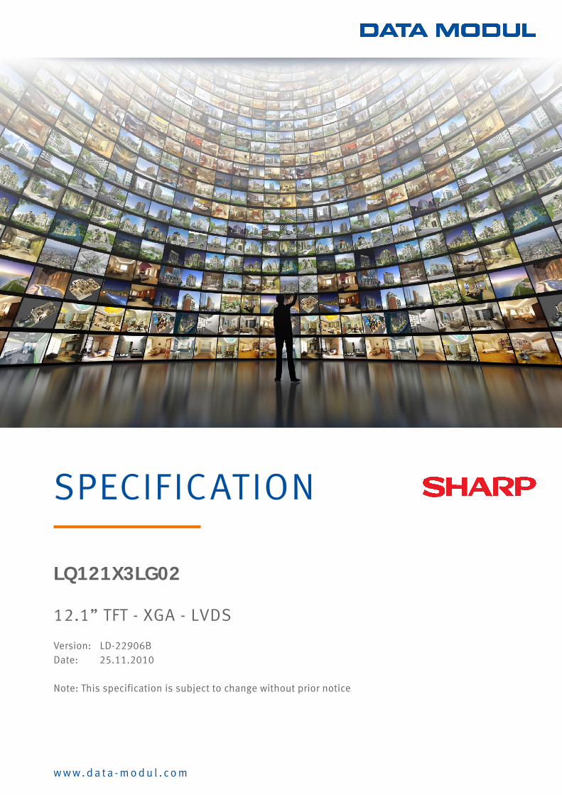
LQ121X3LG02
12.1” TFT - XGA - LVDS
Version: LD-22906BDate: 25.11.2010
Note: This specification is subject to change without prior notice
SPECIFICATION
w w w . d a t a - m o d u l . c o m
Data Modul AG - www.data-modul.com
LD-22906B-1
NOTICE This publication is the proprietary of SHARP and is copyrighted, with all rights reserved. Under the copyright laws, no part of this publication may be reproduced or transmitted in any form or by any means, electronic or mechanical for any purpose, in whole or in part, without the express written permission of SHARP. Express written permission is also required before any use of this publication may be made by a third party. The application circuit examples in this publication are provided to explain the representative applications of SHARP's devices and are not intended to guarantee any circuit design or permit any industrial property right or other rights to be executed. SHARP takes no responsibility for any problems related to any industrial property right or a third party resulting from the use of SHARP's devices, except for those resulting directly from device manufacturing processes. In the absence of confirmation by device specification sheets, SHARP takes no responsibility for any defects that occur in equipment using any of SHARP's devices, shown in catalogs, data books, etc. Contact SHARP in order to obtain the latest device specification sheets before using any SHARP's device. SHARP reserves the right to make changes in the specifications, characteristics, data, materials, structures and other contents described herein at any time without notice in order to improve design or reliability. Contact SHARP in order to obtain the latest specification sheets before using any SHARP's device. Manufacturing locations are also subject to change without notice. Observe the following points when using any device in this publication. SHARP takes no responsibility for damage caused by improper use of the devices. The devices in this publication are designed for use in general electronic equipment designs, such as: - Personal computers - Office automation - Telecommunication equipment - Test and measurement equipment - Industrial control - Personal digital assistant - Audio visual and multimedia equipment - Consumer electronics - Personal navigation device The appropriate design measures should be taken to ensure reliability and safety when SHARP’s devices are used for equipment such as: - Transportation control and safety equipment (i.e., aircraft, trains, automobiles, etc.) - Traffic signals - Gas leakage sensor breakers - Alarm equipment - Various safety devices etc. SHARP's devices shall not be used for equipment that requires extremely high level of reliability, such as: - Military and space applications - Nuclear power control equipment - Medical equipment for life support Contact a SHARP representative, in advance, when intending to use SHARP's devices for any "specific" applications other than those recommended by SHARP. Contact and consult with a SHARP representative if there are any questions about the contents of this
publication.
Data Modul AG - www.data-modul.com
LD-22906B-2
Table of contents 1. Applicable Scope ...................................................................................................................... 3 2. General Description .................................................................................................................. 3 3. Mechanical (Physical) Specifications ....................................................................................... 3 4. Input Terminals ......................................................................................................................... 4 4-1. TFT-LCD panel driving ........................................................................................................ 4 4-2. LVDS interface block diagram ............................................................................................. 5 4-3. Backlight driving................................................................................................................... 6
5. Absolute Maximum Ratings ...................................................................................................... 6 6. Electrical Characteristics .......................................................................................................... 7 6-1. TFT LCD Panel Driving ....................................................................................................... 7 6-2. Back light driving.................................................................................................................. 9 6-3. LVDS input specification.................................................................................................... 10
7. Timing Characteristics of Input Signals .................................................................................. 11 7-1. Timing Characteristics ....................................................................................................... 11 7-2. Input data signals and display position on the screen ...................................................... 12
8. Input Signals, Basic Colors and Gray Scale of Each Color ................................................... 13 9. Optical Characteristics ............................................................................................................ 14 10. Display Quality ...................................................................................................................... 16 11. Handling Precautions ........................................................................................................... 17 13. Reliability Test Items............................................................................................................. 18 14. Lot No. marking .................................................................................................................... 19 14-1. Module Bar code label ..................................................................................................... 19 14-2. Packing bar code label .................................................................................................... 19
15. RoHS.Regulations ................................................................................................................ 20 16. About PFOS .......................................................................................................................... 20 17. Storage conditions ................................................................................................................ 20 Fig1. LCD module packing carton .............................................................................................. 21 Fig2. 12.1XGA Outline Dimensions ............................................................................................ 22
Data Modul AG - www.data-modul.com
LD-22906A -3
1. Applicable Scope This specification applies to a color TFT-LCD Module “LQ121X3LG02”.
2. General Description This module is a color active matrix LCD module incorporating amorphous silicon TFT (Thin Film Transistor).
It is composed of a color TFT-LCD panel, driver ICs, control circuit and power supply circuit and a back light
unit.
Graphics and texts can be displayed on a 1024 x 3 x 768 dots panel with 262,144 colors by using LVDS
(Low Voltage Differential Signaling) to interface and supplying +3.3V DC supply voltage for TFT-LCD panel
driving and supply voltage for back light.
In this TFT-LCD panel, low reflection / color filters of excellent color performance and LED backlights of
high brightness are incorporated to realize brighter and clearer pictures, making this model optimum for use
in multi-media applications.
Optimum viewing direction is 6 o'clock.
LED Backlight-driving DC/DC converter is not built in this module.
3. Mechanical (Physical) Specifications
Item Specifications Unit
Display size 30.7 (12.1” ) diagonal cm
Active area 245.8 (H) × 184.3(V) mm
Pixel format 1024 (H) x 768 (V) pixel
(1Pixel = R+G+B dots) -
Aspect ratio 4 : 3
Pixel pitch 0.240 (H) x 0.240 (V) mm
Pixel configuration R,G,B vertical stripes -
Display mode Normally White -
Surface treatment Antiglare and hard-coating 2H -
Parameter Min. Typ. Max. Unit
Unit outline
dimensions
Width 258.5 259.0 259.5 mm
Height 204.5 205.0 205.5 mm
Depth - 7.5 8.0 mm
Mass [Note 3-1] - 530 550 g
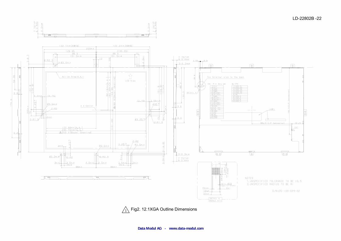
Outline dimensions is shown in Fig.2
[Note 3-1] excluding LED backlight FPC and the mounting tab.
1
Data Modul AG - www.data-modul.com
LD-22906A -4
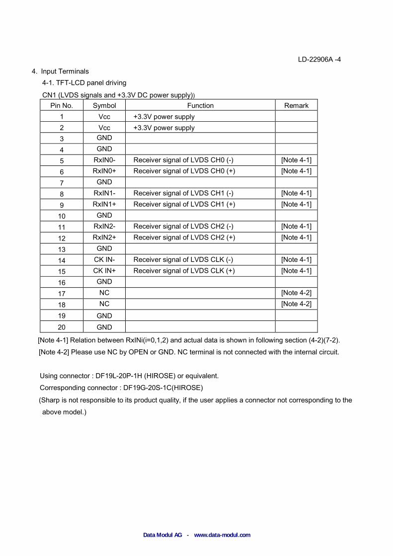
4. Input Terminals 4-1. TFT-LCD panel driving
CN1 (LVDS signals and +3.3V DC power supply)) Pin No. Symbol Function Remark
1 Vcc +3.3V power supply 2 Vcc +3.3V power supply 3 GND 4 GND
5 RxIN0- Receiver signal of LVDS CH0 (-) [Note 4-1]
6 RxIN0+ Receiver signal of LVDS CH0 (+) [Note 4-1]
7 GND
8 RxIN1- Receiver signal of LVDS CH1 (-) [Note 4-1]
9 RxIN1+ Receiver signal of LVDS CH1 (+) [Note 4-1]
10 GND
11 RxIN2- Receiver signal of LVDS CH2 (-) [Note 4-1]
12 RxIN2+ Receiver signal of LVDS CH2 (+) [Note 4-1]
13 GND
14 CK IN- Receiver signal of LVDS CLK (-) [Note 4-1]
15 CK IN+ Receiver signal of LVDS CLK (+) [Note 4-1]
16 GND
17 NC [Note 4-2]
18 NC [Note 4-2]
19 GND 20 GND
[Note 4-1] Relation between RxINi(i=0,1,2) and actual data is shown in following section (4-2)(7-2).
[Note 4-2] Please use NC by OPEN or GND. NC terminal is not connected with the internal circuit.
Using connector : DF19L-20P-1H (HIROSE) or equivalent.
Corresponding connector : DF19G-20S-1C(HIROSE)
(Sharp is not responsible to its product quality, if the user applies a connector not corresponding to the
above model.)
Data Modul AG - www.data-modul.com
LD-22906A -5
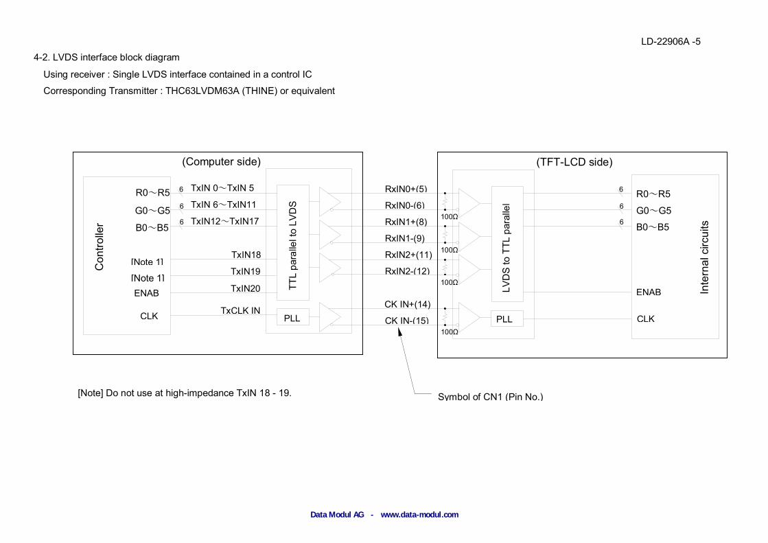
4-2. LVDS interface block diagram
Using receiver : Single LVDS interface contained in a control IC
Corresponding Transmitter : THC63LVDM63A (THINE) or equivalent
TxIN12~TxIN17
TxIN 0~TxIN 5
TxIN 6~TxIN11 R0~R5
B0~B5
ENAB
G0~G5
RxIN0+(5)
RxIN0-(6)
TxIN18
TxIN19
TxIN20
6
6
6
Con
trolle
r
TTL
para
llel t
o LV
DS
PLL
LVD
S to
TTL
par
alle
l
PLL
RxIN1+(8)
RxIN1-(9)
RxIN2+(11)
RxIN2-(12)
CK IN+(14)
CK IN-(15)
6
6
6
R0~R5
B0~B5
ENAB
G0~G5
Inte
rnal
circ
uits
CLK CLK TxCLK IN
(Computer side) (TFT-LCD side)
[Note 1]
[Note 1]
[Note] Do not use at high-impedance TxIN 18 - 19.
100Ω
100Ω
100Ω
100Ω
Symbol of CN1 (Pin No.)
Data Modul AG - www.data-modul.com
LD-22906A -6
4-3. Backlight driving
LED-Back Light FPC Pin No. Symbol Function Remark
1 LED_C1 LED-B/L Cathode1
2 LED_C2 LED-B/L Cathode2
3 LED_C3 LED-B/L Cathode3
4 LED_C4 LED-B/L Cathode4
5 LED_C5 LED-B/L Cathode5
6 NC [Note 4-3]
7 LED_A LED-B/L Anode 8 LED_A LED-B/L Anode 9 LED_A LED-B/L Anode
10 LED_A LED-B/L Anode
[Note 4-3]Please use NC by OPEN. NC terminal is not connected with the internal circuit.
Corresponding connector : 52746-1071(MOLEX)
(Sharp is not responsible to its product quality, if the user applies a connector not corresponding to the
above model.)
5. Absolute Maximum Ratings
Item Symbol Conditions Rated value
Unit Remarks Min. Max.
Input voltage VI Ta = 25°C -0.3 Vcc+0.3 V [Note 5-1]
+3.3V supply voltage Vcc Ta = 25°C 0 +4.0 V
LED forward current ILED_F Ta = 25°C 0 280 mA [Note 5-2]
LED reverse current ILED_R Ta = 25°C ― 85 mA
Storage Temperature Tstg - -35 +75 °C [Note 5-3]
Operating Temperature (Ambient) Topr Ta = 25°C -20 +50 °C [Note 5-3,5-4]
[Note 5-1] LVDS signals [Note 5-2] Value for one LED string [Note 5-3] Humidity:90%RH Max. at Ta≦ +40°C. Maximum wet-bulb temperature at +39°C or less at Ta>+40°C. No condensation. [Note 5-4] Temperature of Panel surface is 60°C Max.
Data Modul AG - www.data-modul.com
LD-22906A -7
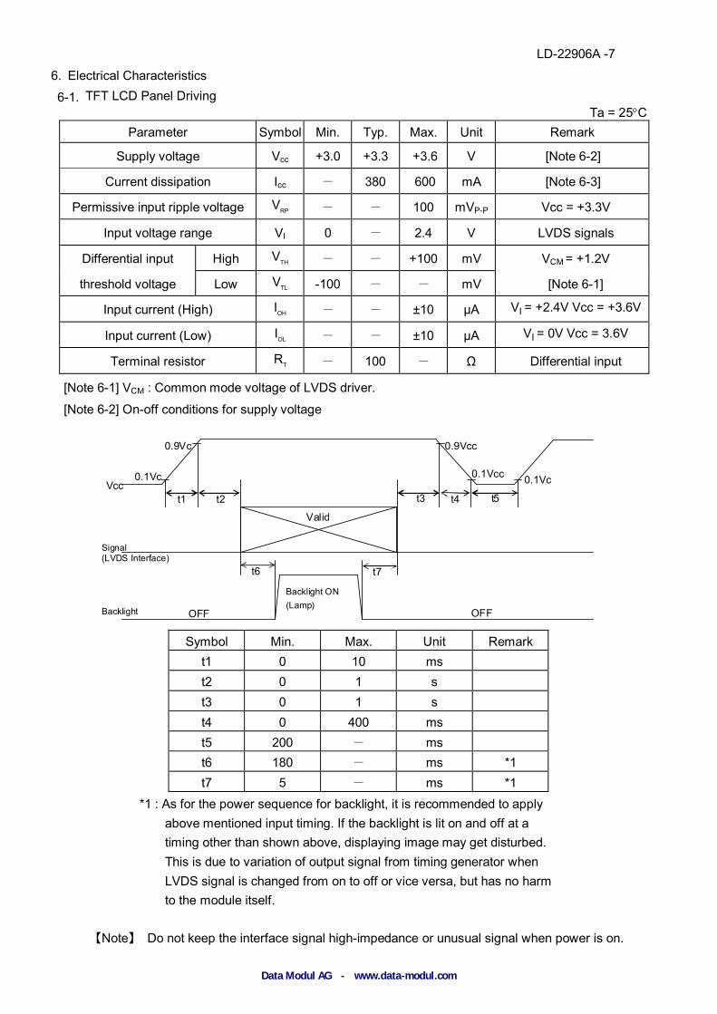
6. Electrical Characteristics
6-1. TFT LCD Panel Driving Ta = 25°C
Parameter Symbol Min. Typ. Max. Unit Remark
Supply voltage Vcc +3.0 +3.3 +3.6 V [Note 6-2]
Current dissipation Icc - 380 600 mA [Note 6-3]
Permissive input ripple voltage VRP - - 100 mVP-P Vcc = +3.3V
Input voltage range VI 0 - 2.4 V LVDS signals
Differential input High VTH - - +100 mV VCM = +1.2V
threshold voltage Low VTL -100 - - mV [Note 6-1]
Input current (High) IOH - - ±10 μA VI = +2.4V Vcc = +3.6V
Input current (Low) IOL - - ±10 μA VI = 0V Vcc = 3.6V
Terminal resistor RT - 100 - Ω Differential input
[Note 6-1] VCM : Common mode voltage of LVDS driver.
[Note 6-2] On-off conditions for supply voltage
Symbol Min. Max. Unit Remark t1 0 10 ms t2 0 1 s t3 0 1 s t4 0 400 ms t5 200 - ms t6 180 - ms *1 t7 5 - ms *1
*1 : As for the power sequence for backlight, it is recommended to apply above mentioned input timing. If the backlight is lit on and off at a timing other than shown above, displaying image may get disturbed. This is due to variation of output signal from timing generator when LVDS signal is changed from on to off or vice versa, but has no harm to the module itself.
【Note】 Do not keep the interface signal high-impedance or unusual signal when power is on.
t1 t2
t6
0.9Vcc 0.9Vc
Vcc
Valid
Backlight
Signal (LVDS Interface)
0.1Vc 0.1Vcc 0.1Vc
t3 t5
OFF OFF
Backlight ON (Lamp)
t7
t4
Data Modul AG - www.data-modul.com
LD-22906A -8
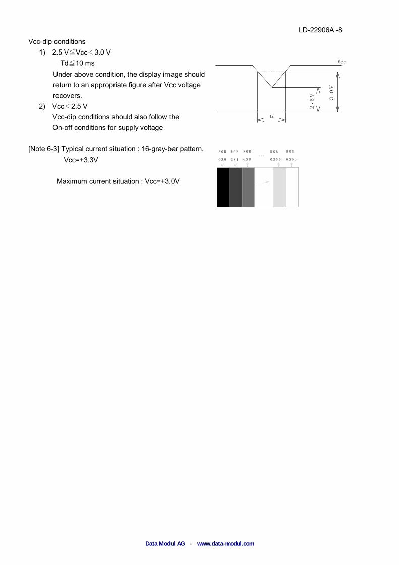
Vcc-dip conditions 1) 2.5 V≦Vcc<3.0 V Td≦10 ms
Under above condition, the display image should return to an appropriate figure after Vcc voltage recovers.
2) Vcc<2.5 V Vcc-dip conditions should also follow the On-off conditions for supply voltage
[Note 6-3] Typical current situation : 16-gray-bar pattern. Vcc=+3.3V
Maximum current situation : Vcc=+3.0V
Vcc
td
3
.
0
V
2
. 5
V
R G B G S 0
R G B G S 4
R G B G S 8
R G B G S 5 6
R G B G S 6 0
. . . .
Data Modul AG - www.data-modul.com
LD-22906A -9
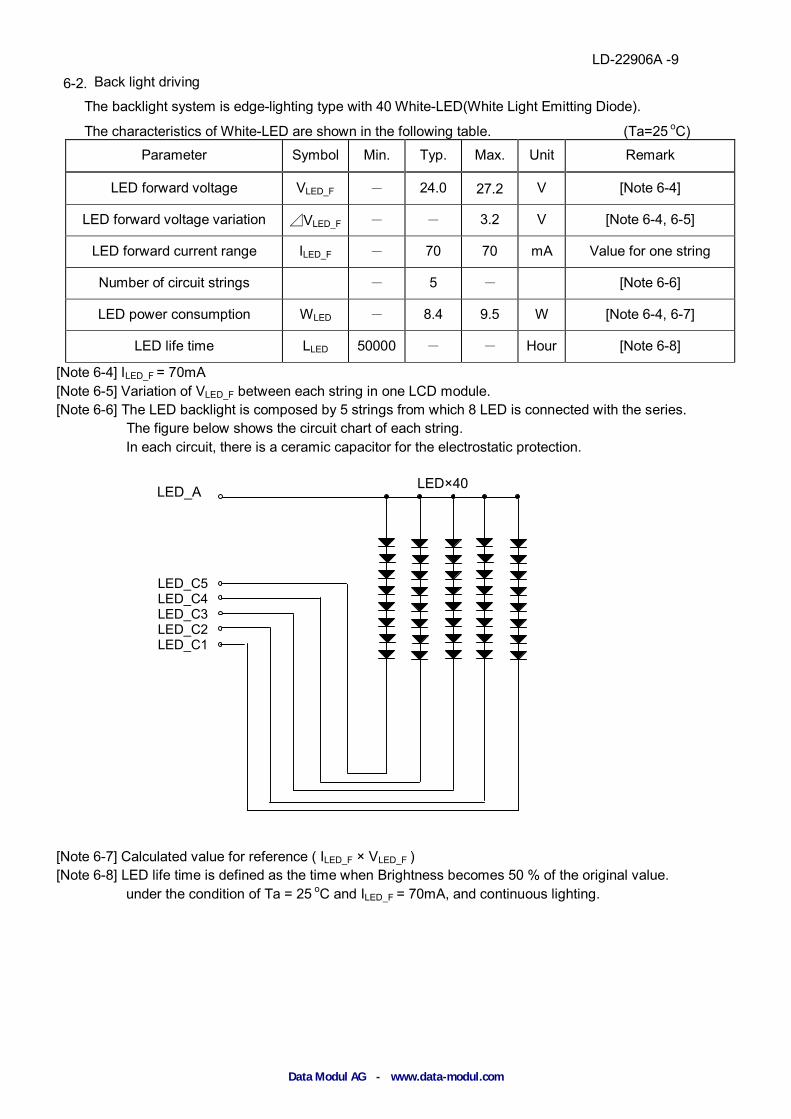
6-2. Back light driving
The backlight system is edge-lighting type with 40 White-LED(White Light Emitting Diode).
The characteristics of White-LED are shown in the following table. (Ta=25 oC) Parameter Symbol Min. Typ. Max. Unit Remark
LED forward voltage VLED_F - 24.0 27.2 V [Note 6-4]
LED forward voltage variation ⊿VLED_F - - 3.2 V [Note 6-4, 6-5]
LED forward current range ILED_F - 70 70 mA Value for one string
Number of circuit strings - 5 - [Note 6-6]
LED power consumption WLED - 8.4 9.5 W [Note 6-4, 6-7]
LED life time LLED 50000 - - Hour [Note 6-8]
[Note 6-4] ILED_F = 70mA [Note 6-5] Variation of VLED_F between each string in one LCD module. [Note 6-6] The LED backlight is composed by 5 strings from which 8 LED is connected with the series. The figure below shows the circuit chart of each string.
In each circuit, there is a ceramic capacitor for the electrostatic protection. [Note 6-7] Calculated value for reference ( ILED_F × VLED_F ) [Note 6-8] LED life time is defined as the time when Brightness becomes 50 % of the original value.
under the condition of Ta = 25 oC and ILED_F = 70mA, and continuous lighting.
LED_A
LED_C5 LED_C4 LED_C3 LED_C2 LED_C1
LED×40
Data Modul AG - www.data-modul.com
LD-22906A -10
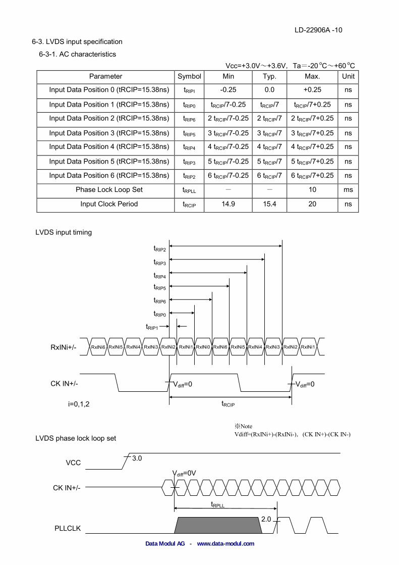
6-3. LVDS input specification
6-3-1. AC characteristics Vcc=+3.0V~+3.6V,Ta=-20 oC~+60 oC
Parameter Symbol Min Typ. Max. Unit
Input Data Position 0 (tRCIP=15.38ns) tRIPI -0.25 0.0 +0.25 ns
Input Data Position 1 (tRCIP=15.38ns) tRIP0 tRCIP/7-0.25 tRCIP/7 tRCIP/7+0.25 ns
Input Data Position 2 (tRCIP=15.38ns) tRIP6 2 tRCIP/7-0.25 2 tRCIP/7 2 tRCIP/7+0.25 ns
Input Data Position 3 (tRCIP=15.38ns) tRIP5 3 tRCIP/7-0.25 3 tRCIP/7 3 tRCIP/7+0.25 ns
Input Data Position 4 (tRCIP=15.38ns) tRIP4 4 tRCIP/7-0.25 4 tRCIP/7 4 tRCIP/7+0.25 ns
Input Data Position 5 (tRCIP=15.38ns) tRIP3 5 tRCIP/7-0.25 5 tRCIP/7 5 tRCIP/7+0.25 ns
Input Data Position 6 (tRCIP=15.38ns) tRIP2 6 tRCIP/7-0.25 6 tRCIP/7 6 tRCIP/7+0.25 ns
Phase Lock Loop Set tRPLL - - 10 ms
Input Clock Period tRCIP 14.9 15.4 20 ns
LVDS input timing
LVDS phase lock loop set
i=0,1,2 tRCIP
CK IN+/- Vdiff=0 Vdiff=0
tRIP1
tRIP0
tRIP6
tRIP5 tRIP4
tRIP3
tRIP2
RxINi6 RxINi5 RxINi4 RxINi3 RxINi2 RxINi1 RxINi0 RxINi6 RxINi5 RxINi4 RxINi3 RxINi2 RxINi1 RxINi+/-
※Note Vdiff=(RxINi+)-(RxINi-),(CK IN+)-(CK IN-)
3.0
tRPLL
VCC
CK IN+/-
PLLCLK 2.0
Vdiff=0V
Data Modul AG - www.data-modul.com
LD-22906A -11
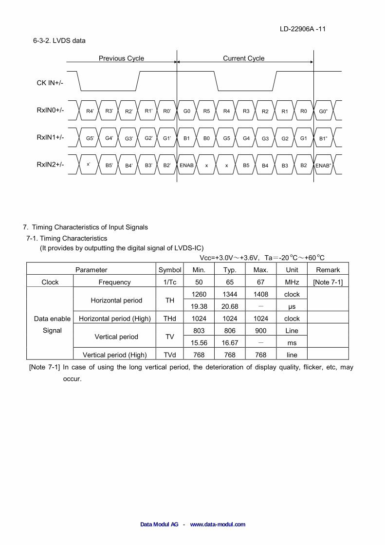
6-3-2. LVDS data
7. Timing Characteristics of Input Signals 7-1. Timing Characteristics
(It provides by outputting the digital signal of LVDS-IC) Vcc=+3.0V~+3.6V,Ta=-20 oC~+60 oC
Parameter Symbol Min. Typ. Max. Unit Remark
Clock Frequency 1/Tc 50 65 67 MHz [Note 7-1]
Data enable
Signal
Horizontal period TH 1260 1344 1408 clock
19.38 20.68 - μs
Horizontal period (High) THd 1024 1024 1024 clock
Vertical period TV 803 806 900 Line
15.56 16.67 - ms
Vertical period (High) TVd 768 768 768 line
[Note 7-1] In case of using the long vertical period, the deterioration of display quality, flicker, etc, may
occur.
CK IN+/-
R4’ R3’ R2’ R1’ R0’ G0 R5 R4 R3 R2 R1 R0 G0” RxIN0+/-
G5’ G4’ G3’ G2’ G1’ B1 B0 G5 G4 G3 G2 G1 B1” RxIN1+/-
x’ B5’ B4’ B3’ B2’ ENAB x x B5 B4 B3 B2 ENAB” RxIN2+/-
Previous Cycle Current Cycle
Data Modul AG - www.data-modul.com
LD-22906A -12
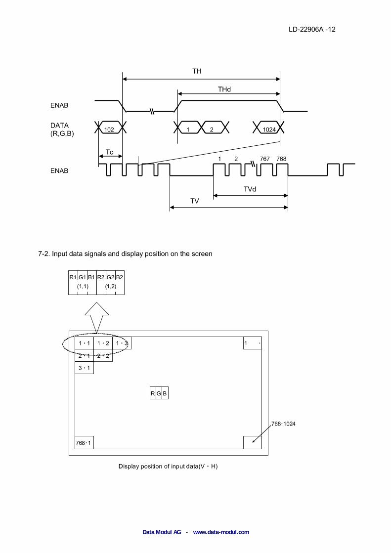
7-2. Input data signals and display position on the screen
1・1 1・2 1・3
2・1 2・2
3・1
768・1
1 ・
R G B
768・1024
R1 G1 B1 R2 G2 B2 (1,1) (1,2)
Display position of input data(V・H)
102 1 2 1024
THd
TVd
TV
Tc 1 2 768
ENAB
DATA (R,G,B)
ENAB
767
TH
Data Modul AG - www.data-modul.com
LD-22906A -13
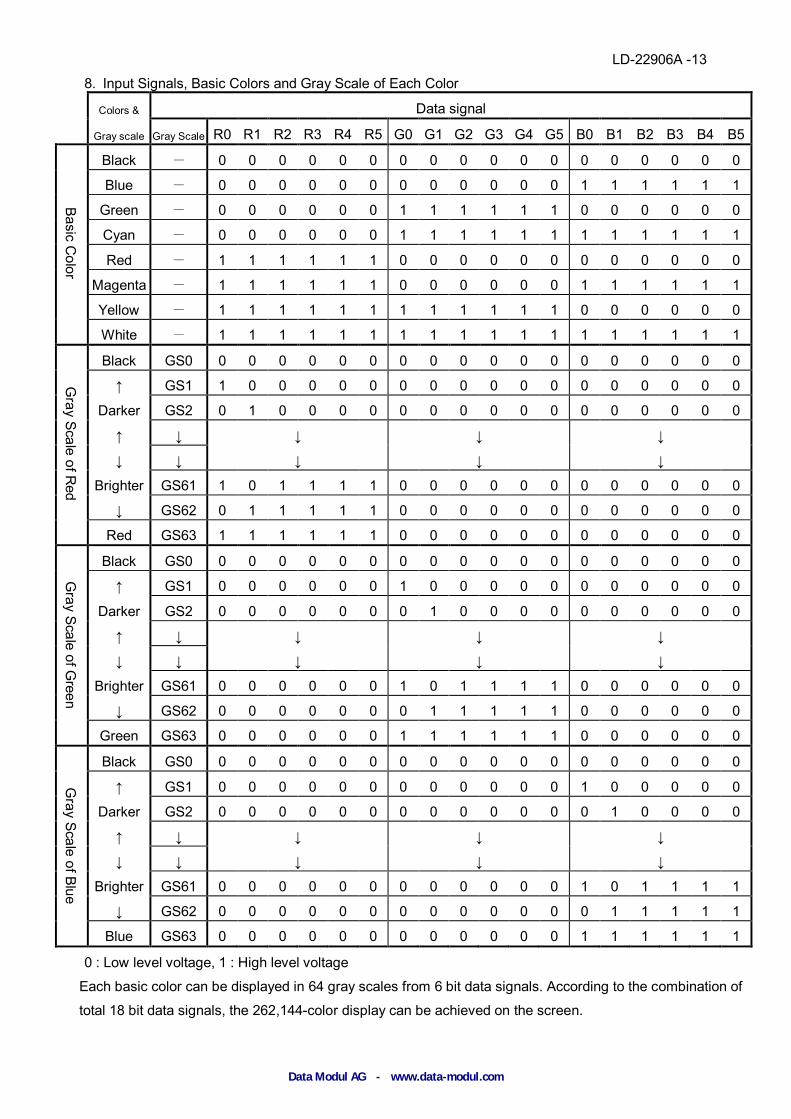
8. Input Signals, Basic Colors and Gray Scale of Each Color
Colors & Data signal
Gray scale Gray Scale R0 R1 R2 R3 R4 R5 G0 G1 G2 G3 G4 G5 B0 B1 B2 B3 B4 B5
Black - 0 0 0 0 0 0 0 0 0 0 0 0 0 0 0 0 0 0
Blue - 0 0 0 0 0 0 0 0 0 0 0 0 1 1 1 1 1 1
Green - 0 0 0 0 0 0 1 1 1 1 1 1 0 0 0 0 0 0
Cyan - 0 0 0 0 0 0 1 1 1 1 1 1 1 1 1 1 1 1
Red - 1 1 1 1 1 1 0 0 0 0 0 0 0 0 0 0 0 0
Magenta - 1 1 1 1 1 1 0 0 0 0 0 0 1 1 1 1 1 1
Yellow - 1 1 1 1 1 1 1 1 1 1 1 1 0 0 0 0 0 0
White - 1 1 1 1 1 1 1 1 1 1 1 1 1 1 1 1 1 1
Black GS0 0 0 0 0 0 0 0 0 0 0 0 0 0 0 0 0 0 0
↑ GS1 1 0 0 0 0 0 0 0 0 0 0 0 0 0 0 0 0 0
Darker GS2 0 1 0 0 0 0 0 0 0 0 0 0 0 0 0 0 0 0
↑ ↓ ↓ ↓ ↓
↓ ↓ ↓ ↓ ↓
Brighter GS61 1 0 1 1 1 1 0 0 0 0 0 0 0 0 0 0 0 0
↓ GS62 0 1 1 1 1 1 0 0 0 0 0 0 0 0 0 0 0 0
Red GS63 1 1 1 1 1 1 0 0 0 0 0 0 0 0 0 0 0 0
Black GS0 0 0 0 0 0 0 0 0 0 0 0 0 0 0 0 0 0 0
↑ GS1 0 0 0 0 0 0 1 0 0 0 0 0 0 0 0 0 0 0
Darker GS2 0 0 0 0 0 0 0 1 0 0 0 0 0 0 0 0 0 0
↑ ↓ ↓ ↓ ↓
↓ ↓ ↓ ↓ ↓
Brighter GS61 0 0 0 0 0 0 1 0 1 1 1 1 0 0 0 0 0 0
↓ GS62 0 0 0 0 0 0 0 1 1 1 1 1 0 0 0 0 0 0
Green GS63 0 0 0 0 0 0 1 1 1 1 1 1 0 0 0 0 0 0
Black GS0 0 0 0 0 0 0 0 0 0 0 0 0 0 0 0 0 0 0
↑ GS1 0 0 0 0 0 0 0 0 0 0 0 0 1 0 0 0 0 0
Darker GS2 0 0 0 0 0 0 0 0 0 0 0 0 0 1 0 0 0 0
↑ ↓ ↓ ↓ ↓
↓ ↓ ↓ ↓ ↓
Brighter GS61 0 0 0 0 0 0 0 0 0 0 0 0 1 0 1 1 1 1
↓ GS62 0 0 0 0 0 0 0 0 0 0 0 0 0 1 1 1 1 1
Blue GS63 0 0 0 0 0 0 0 0 0 0 0 0 1 1 1 1 1 1
0 : Low level voltage, 1 : High level voltage
Each basic color can be displayed in 64 gray scales from 6 bit data signals. According to the combination of
total 18 bit data signals, the 262,144-color display can be achieved on the screen.
Basic Color
Gray Scale of R
ed G
ray Scale of Green
Gray Scale of Blue
Data Modul AG - www.data-modul.com
LD-22906A -14
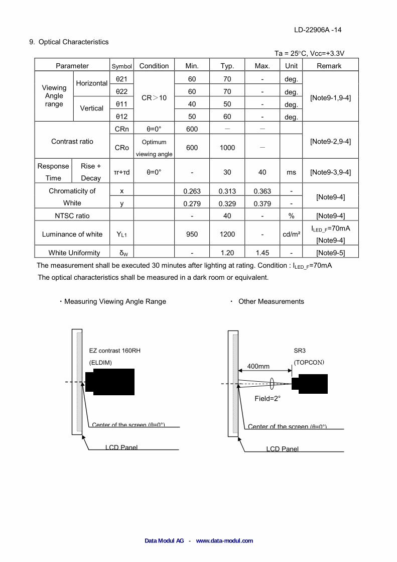
9. Optical Characteristics Ta = 25°C, Vcc=+3.3V
Parameter Symbol Condition Min. Typ. Max. Unit Remark
Viewing Angle range
Horizontal θ21
CR>10
60 70 - deg.
[Note9-1,9-4] θ22 60 70 - deg.
Vertical θ11 40 50 - deg.
θ12 50 60 - deg.
Contrast ratio
CRn θ=0° 600 - -
[Note9-2,9-4] CRo
Optimum
viewing angle 600 1000 -
Response
Time
Rise +
Decay τr+τd θ=0° - 30 40 ms [Note9-3,9-4]
Chromaticity of
White
x 0.263 0.313 0.363 - [Note9-4]
y 0.279 0.329 0.379 -
NTSC ratio - 40 - % [Note9-4]
Luminance of white YL1 950 1200 - cd/m² ILED_F=70mA
[Note9-4]
White Uniformity δW - 1.20 1.45 - [Note9-5]
The measurement shall be executed 30 minutes after lighting at rating. Condition : ILED_F=70mA
The optical characteristics shall be measured in a dark room or equivalent.
・Measuring Viewing Angle Range ・ Other Measurements
EZ contrast 160RH
(ELDIM)
Center of the screen (θ=0°)
LCD Panel
Center of the screen (θ=0°)
400mm
Field=2°
SR3
(TOPCON)
LCD Panel
Data Modul AG - www.data-modul.com
LD-22906A -15
90%
10%
受光器出力(
相対値)
黒
白
τd
90%
10%
黒
白
τr
時間
Black Black
white white
Photo detector output
(Relative value)
Time
τd τr
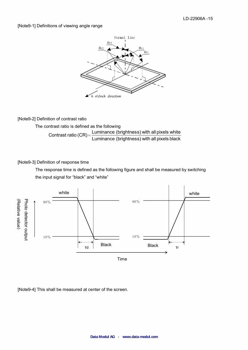
[Note9-1] Definitions of viewing angle range
[Note9-2] Definition of contrast ratio
The contrast ratio is defined as the following
black pixels all withs)(brightnes Luminance whitepixels all withs)(brightnes Luminance(CR) ratio ontrastC =
[Note9-3] Definition of response time
The response time is defined as the following figure and shall be measured by switching
the input signal for “black” and “white”
[Note9-4] This shall be measured at center of the screen.
Data Modul AG - www.data-modul.com
LD-22906A -16
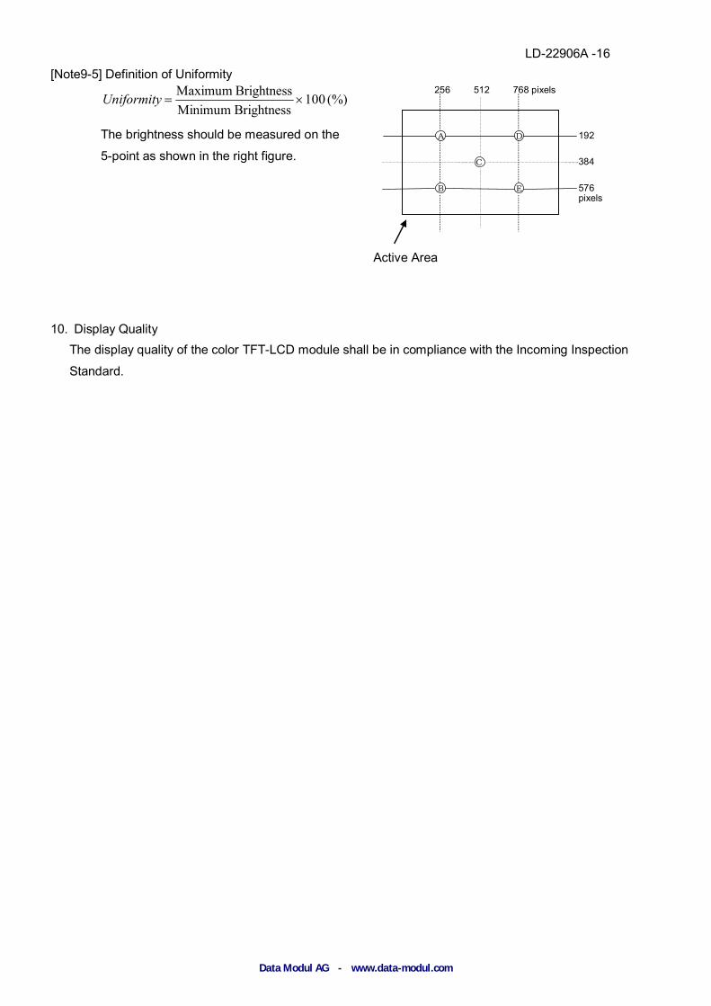
[Note9-5] Definition of Uniformity
(%)100Brightness MinimumBrightness Maximum
´=Uniformity
The brightness should be measured on the
5-point as shown in the right figure.
10. Display Quality The display quality of the color TFT-LCD module shall be in compliance with the Incoming Inspection
Standard.
D A
C
E
B
768 pixels 512 256
192
384
pixels 576
Active Area
Data Modul AG - www.data-modul.com
LD-22906A -17
11. Handling Precautions a) Be sure to turn off the power supply when inserting or disconnecting the cable.
b) Be sure to design the cabinet so that the module can be installed without any extra stress such as warp or twist.
c) Since the front polarizer is easily damaged, pay attention not to scratch it. Blow away dust on the polarizer with antistatic N2 blow. It is undesirable to wipe off because a polarizer is sensitive. It is recommended to peel off softly using the adhesive tape when soil or finger oil is stuck to the polarizer. When unavoidable, wipe off carefully with a cloth for wiping lenses.
d) Wipe off water drop immediately. Long contact with water may cause discoloration or spots. e) When the panel surface is soiled, wipe it with absorbent cotton or other soft cloth. f) Since the panel is made of glass, it may break or crack if dropped or bumped on hard surface. Handle with care. g) Since CMOS LSI is used in this module, take care of static electricity and injure the human earth when
handling. Observe all other precautionary requirements in handling components.
h) Since there is a circuit board in the module back, stress is not added at the time of a design assembly. Please make it like. If stress is added, there is a possibility that circuit parts may be damaged.
i) Protection film is attached to the module surface to prevent it from being scratched . Peel the film off slowly , just before the use, with strict attention to electrostatic charges.
Blow off 'dust' on the polarizer by using an ionized nitrogen. j) Do not expose the LCD module to a direct sunlight, for a long period of time to protect the module from
the ultra violet ray. k) Connect GND of mounting holes to stabilize against EMI and external noise. l) When handling LCD modules and assembling them into cabinets, please avoid that long-terms storage in
the environment of oxidization or deoxidization gas and the use of such materials as reagent, solvent, adhesive, resin, etc. which generate these gasses, may cause corrosion and discoloration of the
modules. m) Liquid crystal contained in the panel may leak if the LCD is broken. Rinse it as soon as possible if it gets
inside your eye or mouth by mistake. n) Notice : Never dismantle the module , because it will cause failure.
Please don't remove the fixed tape, insulating tape etc that was pasted on the original module. (Except for protection film of the panel and the crepe tape (yellow tape) of fixing LED FPC temporarily.)
o) Be careful when using it for long time with fixed pattern display as it may cause afterimage. (Please use a screen saver etc., in order to avoid an afterimage.) p) Adjusting volume has been set optimally before shipment, so do not change any adjusted value. If adjusted value is changed, the specification may not be satisfied. q) Please note that it is likely to damage your eyes when keeping seeing for a long time for a high
luminance specification.
Data Modul AG - www.data-modul.com
LD-22906A -18
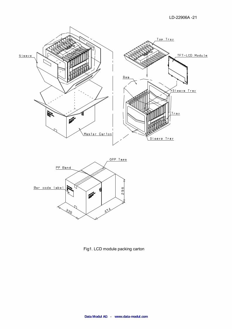
12. Packing form This packing form and the specification are tentative. This packing form and specification might be changed because they are designing now.
Piling number of cartons Max 6
Package quantity in one carton 10 pcs
Carton size 474(W)×335(D)×296(H)mm
Total mass of one carton filled with full modules 7500g
Packing form Fig.1
13. Reliability Test Items
No. Test item Conditions 1 High temperature storage test Ta = 75°C 96h 2 Low temperature storage test Ta = -35°C 96h
3 High temperature & high humidity operation test
(Ta = 40°C ; 90%RH 120h) (No condensation)
4 High temperature operation test Ta = 50°C 24h (Temperature of Panel surface is 60°C Max)
5 Low temperature operation test Ta = -20°C 24h
6 Thermal Shock Test (non- operating)
+75oC(0.5hours) ⇔ -35 oC(0.5hours) Tested for 100 cycles
7 Vibration test (non- operating)
Frequency range: 10 to 57Hz Sweep: 0.076mm 57 to 500Hz Acceleration:9.8m/s2
Sweep time: 11minute Test period: 3 hours (1 hours for each direction of X,Y,Z)
8 Shock test (non- operating)
Direction: ±X, ±Y, ±Z, Time: 1 times for each direction. Impact value: 490m/s², Action time 11ms
9 Electro static discharge test (non-operating)
Bezel/Panel :IEC61000-4-2 Contact ±10kV Air ±20kV (LCD module is placed on an insulated board and examined.)
10 Electro static discharge test (operating)
Bezel/Panel :IEC61000-4-2 Contact ±8kV Air ±15kV (LCD module is placed on an insulated board and examined.)
[Result Evaluation Criteria]
Under the display quality test conditions with normal operation state, these shall be no change which may
affect practical display function.
normal operation state:Temperature:15~35°C, Humidity:45~75%, Atmospheric pressure:86~106kpa
(based on JIS Z 8703)
Data Modul AG - www.data-modul.com
LD-22906A -19
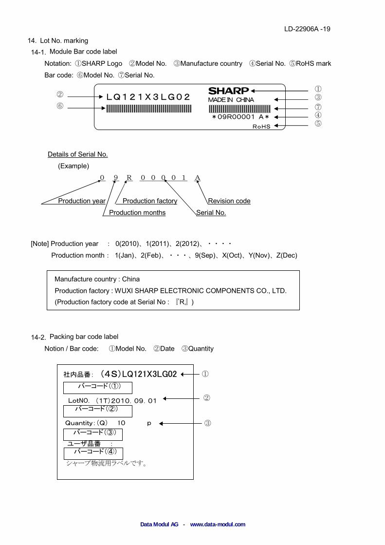
14. Lot No. marking
14-1. Module Bar code label
Notation: ①SHARP Logo ②Model No. ③Manufacture country ④Serial No. ⑤RoHS mark
Bar code: ⑥Model No. ⑦Serial No.
Details of Serial No.
(Example)
0 9 R 0 0 0 0 1 A
Production year Production factory Revision code
Production months Serial No.
[Note] Production year : 0(2010)、1(2011)、2(2012)、・・・・
Production month: 1(Jan)、2(Feb)、・・・、9(Sep)、X(Oct)、Y(Nov)、Z(Dec)
Manufacture country : China
Production factory : WUXI SHARP ELECTRONIC COMPONENTS CO., LTD. (Production factory code at Serial No : 『R』)
14-2. Packing bar code label
Notion / Bar code: ①Model No. ②Date ③Quantity
*09R00001 A*
MADE IN CHINA LQ121X3LG02 ②
⑥
① ③
⑦ ④
RoHS ⑤
社内品番: (4S)LQ121X3LG02
LotNO. (1T)2010.09.01
Quantity:(Q) 10 p
ユーザ品番 :
バーコード(①)
バーコード(②)
バーコード(③)
シャープ物流用ラベルです。
①
②
③
バーコード(④)
Data Modul AG - www.data-modul.com
LD-22906A -20
15. RoHS.Regulations This LCD module is compliant with RoHS Directive.
16. About PFOS This module doesn't do intentional use about PFOS (perfluorooctanesulfonic acid) and the salt.
17. Storage conditions <Environmental condition range of storage temperature and humidity>
Temperature 0 to 40 degrees Celsius
Relative humidity 90% and below
Direct sun light
Please keep the product in a dark room or cover the product to protect from direct sun light.
Atmospheric condition
Please refrain from keeping the product with possible corrosive gas or volatile flux.
Prevention of dew
* Please store the product carton either on a wooden pallet or a stand / rak to prevent dew.
Do not place directly on the floor. In addition, to obtain moderate ventilation in between the pallet’s
top and bottom surfaces, pile the cartons up in a single direction and in order.
* Please place the product cartons away from the strage wall.
* Please maintain the storage area with an appropriate ventilation. It is recommendable to furnish
the storage area with equipments such as ventilation systems.
* Please maintain the ambient temperature within the range of natural environmental fluctuation.
Storage period
Within above mentioned conditions, maximum storage period should be one year.
Data Modul AG - www.data-modul.com
LD-22906A -21
Fig1. LCD module packing carton
Data Modul AG - www.data-modul.com
LD-22802B -22
Fig2. 12.1XGA Outline Dimensions 1
Data Modul AG - www.data-modul.com

A L L T E C H N O LO G I E S . A L L CO M P E T E N C I E S . O N E S P E C I A L I S T.
w w w . d a t a - m o d u l . c o m
More information and worldwide locations can be found at
DATA MODUL AG
Landsberger Straße 322 DE-80687 Munich Phone: +49-89-56017-0
DATA MODUL WEIKERSHEIM GMBH
Lindenstraße 8 DE-97990 Weikersheim Phone: +49-7934-101-0


![Sharp LS044Q7DH01 TFT-Display distributed by DATA MODUL AG · [For handling and system design] (1) Handle with care as glass is used in this LCD panel. Dropping or contact against](https://img.pdfslide.net/doc/110x75/5e1790bb0a43fe475a068126/sharp-ls044q7dh01-tft-display-distributed-by-data-modul-ag-for-handling-and-system.jpg)