Embed Size (px)
Citation preview
CHAPTER 1
INTRODUCTION TO EMBEDDED SYSTEMS
An Embedded system is a system which consists of hard ware and soft ware
which works for specific purpose only, a particular program will be embedded in it and it
will be running repeatedly. But a desktop system is not like that it will run for different
purposes.
An embedded system is a microcontroller-based, software driven, reliable, real-
time control system, autonomous, or human or network interactive, operating on diverse
physical variables and in diverse environments and sold into a competitive and cost
conscious market. It is expected to function with minimal human intervention. It is a
time-constrained and often resource-constrained. It can be existed from aerospace to
earth.
Embedded Systems characteristics are,
1) Single function.
2) High performance.
3) Safety.
4) Size.
5) Real time oriented.
6) Operated at harsh environments.
7) Easy handling.
1.1 Attributes of an embedded system:
As embedded systems started progressing, they started becoming more and more
complex. Not only were the embedded devices able to do their jobs but also were able to
do them smartly. These attributes can be defined as,
Computational power: These devices have some amount of computing power. A
very simple 8-bit controller or a high-end 64-bit microprocessor could provide
this computation power.
Memory: The next requirement is memory. These devices possess some amount
of memory that can be used by the processor and also some to remember user data
and preferences.
Realtime: All the devices have to respond to user/environmental inputs within a
specified period of time.
Communication: The device must be able to receive inputs given by other devices
in the environment, process it and provide some solid output to the other devices
or users.
Dynamic decisions: The system should be able to change its next course of
activity based on the change of input from its sensors or surroundings.
Whether the benefits are in concerned with security purposes or with human’s
comforts, in fact these intelligent systems helped humanity in every phase of life. They
have helped man in their progress by developing the new technologies. Embedded
microprocessors enable firms to compete on product and service innovation, by adding
product and service features that customer’s value, but which would be largely
impossible without this technology. According to market researchers, consumers love
electronic equipment that can do “smart” things like transmit instructions to other devices
wirelessly via infrared signals be programmed to operate automatically and connect to
super-technologies such as satellites, to bring remote power into their own hands. Such
systems have made their life easy and comfortable. Thus in short such systems have
facilitated, by fulfilling the needs of a man or giving him luxuries. Several reasons that
development of embedded systems is more difficult than development of any other
software are as follows
Complexity: The designing of embedded systems is more complex than any other
software.
Testing: There are more failure cases, therefore correctness is often more
important.
Predictability: The performance of a system must be predictable in order for
people to have confidence in it. If the performance is variable, then one is never
sure that the system will meet its resource requirements on any given execution.
Specification: The specifications of an embedded system must be more detailed.
Domain knowledge: The programmers must have more domain knowledge than
usual.
1.2 Applications of embedded systems:
Aerospace & defense electronics.
Telemetric.
Broadcast & entertainment.
Internet appliances.
Data communication.
Automatic teller machines.
Computer printers.
Household appliances, including microwave ovens, air conditioners, washing
machines, and television sets.
Network equipment, including routers and firewalls.
Engine control computers and antilock brake controllers for automobiles.
Traffic control (e.g.: Intelligent traffic lights )
Music systems.
The details of the embedded systems such as its characteristics, its components,
the challenges programmer faces while designing such systems, its practical
implementations, its importance in daily life and its future prospects. In short, embedded
systems play an important role in our daily life work. This technology has made our lives
easier and in few decades, it would probably change the outlook of this world.
CHAPTER 2
AT89C51 MICROCONTROLLER
2.1 Introduction:
The AT89C51 is a low-power, high-performance CMOS 8-bit microcomputer
with 4K bytes of Flash programmable and erasable read only memory (PEROM). The
device is manufactured using Atmel’s high-density nonvolatile memory technology and
is compatible with the industry-standard MCS-51 instruction set and pinout. The on-chip
Flash allows the program memory to be reprogrammed in-system or by a conventional
nonvolatile memory programmer. By combining a versatile 8-bit CPU with Flash on a
monolithic chip, the Atmel AT89C51 is a powerful microcomputer which provides a
highly-flexible and cost-effective solution to many embedded control applications.
2.2 Features:
Compatible with MCS-51™ Products
4K Bytes of In-System Reprogrammable Flash Memory
Endurance: 1,000 Write/Erase Cycles
Fully Static Operation: 0 Hz to 24 MHz
Three-level Program Memory Lock
128 x 8-bit Internal RAM
32 Programmable I/O Lines
Two 16-bit Timer/Counters
Six Interrupt Sources
Programmable Serial Channel
Low-power Idle and Power-down Modes
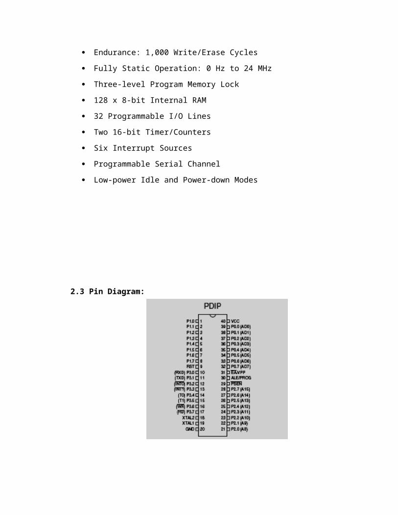
2.3 Pin Diagram:
Figure 2.1: Pin diagram of AT89C51
2.4 Pin Description:
VCC: Supply voltage.
GND: Ground.
Port 0:Port 0 is an 8-bit open-drain bi-directional I/O port. As an output port, each pin
can sink eight TTL inputs. When 1s are written to port 0 pins, the pins can be used as
high- impedance inputs.
Port 0 may also be configured to be the multiplexed low- order address/data bus
during accesses to external program and data memory. In this mode P0 has internal pull
ups.
Port 0 also receives the code bytes during Flash programming and outputs the
code bytes during program verification. External pull ups are required during program
verification.
Port 1:
Port 1 is an 8-bit bi-directional I/O port with internal ull-ups. The Port 1 output
buffers can sink/source four TTL inputs. When 1s are written to Port 1 pins they are
pulled high by the internal pull-ups and can be used as inputs. As inputs, Port 1 pins that
are externally being pulled low will source current (IIL) because of the internal pull-ups.
Port 1 also receives the low-order address bytes during Flash programming and
verification.
Port 2:
Port 2 is an 8-bit bi-directional I/O port with internal pullups. The Port 2 output
buffers can sink/source four TTL inputs. When 1s are written to Port 2 pins they are
pulled high by the internal pullups and can be used as inputs. As inputs,Port 2 pins that
are externally being pulled low will source current (IIL) because of the internal pullups.
Port 2 emits the high-order address byte during fetches from external program
memory and during accesses to external data memory that uses 16-bit addresses (MOVX
@ DPTR). In this application, it uses strong internal pullups when emitting 1s. During
accesses to external data memory that uses 8-bit addresses (MOVX @ RI), Port 2 emits
the contents of the P2 Special Function Register.
Port 2 also receives the high-order address bits and some control signals during
Flash programming and verification.
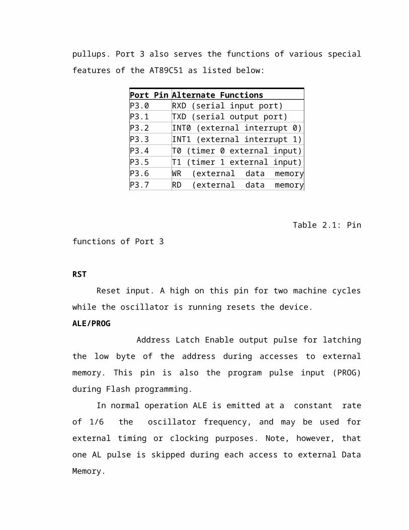
Port 3:
Port 3 is an 8-bit bi-directional I/O port with internal pullups. The Port 3 output
buffers can sink/source four TTL inputs. When 1s are written to Port 3 pins they are
pulled high by the internal pullups and can be used as inputs. As inputs, Port 3 pins that
are externally being pulled low will source current (IIL) because of the pullups. Port 3
also serves the functions of various special features of the AT89C51 as listed below:
Table 2.1: Pin functions of Port 3
RST
Port Pin Alternate FunctionsP3.0 RXD (serial input port)P3.1 TXD (serial output port)P3.2 INT0 (external interrupt 0)P3.3 INT1 (external interrupt 1)P3.4 T0 (timer 0 external input)P3.5 T1 (timer 1 external input)P3.6 WR (external data memory write strobe)P3.7 RD (external data memory read strobe)
Reset input. A high on this pin for two machine cycles while the oscillator is
running resets the device.
ALE/PROG
Address Latch Enable output pulse for latching the low byte of the address during
accesses to external memory. This pin is also the program pulse input (PROG) during
Flash programming.
In normal operation ALE is emitted at a constant rate of 1/6 the oscillator
frequency, and may be used for external timing or clocking purposes. Note, however, that
one AL pulse is skipped during each access to external Data Memory.
If desired, ALE operation can be disabled by setting bit 0 of SFR location 8EH.
With the bit set, ALE is active only during a MOVX or MOVC instruction. Otherwise,
the pin is weakly pulled high. Setting the ALE-disable bit has no effect if the
microcontroller is in external execution mode.
PSEN
Program Store Enable is the read strobe to external pro- gram memory. When the
AT89C51 is executing code from external program memory, PSEN is activated twice
each machine cycle, except that two PSEN activations are skipped during each access to
external data memory.
EA/VPP
External Access Enable. EA must be strapped to GND in order to enable the
device to fetch code from external pro- gram memory locations starting at 0000H up to
FFFFH. Note, however, that if lock bit 1 is programmed, EA will be internally latched on
reset. EA should be strapped to V CC for internal program executions. This pin also
receives the 12-volt programming enable volt- age (VPP) during Flash programming, for
parts that require12-volt VPP.
XTAL1
Input to the inverting oscillator amplifier and input to the internal clock operating
circuit.
XTAL2
This is an Output from the inverting oscillator amplifier.
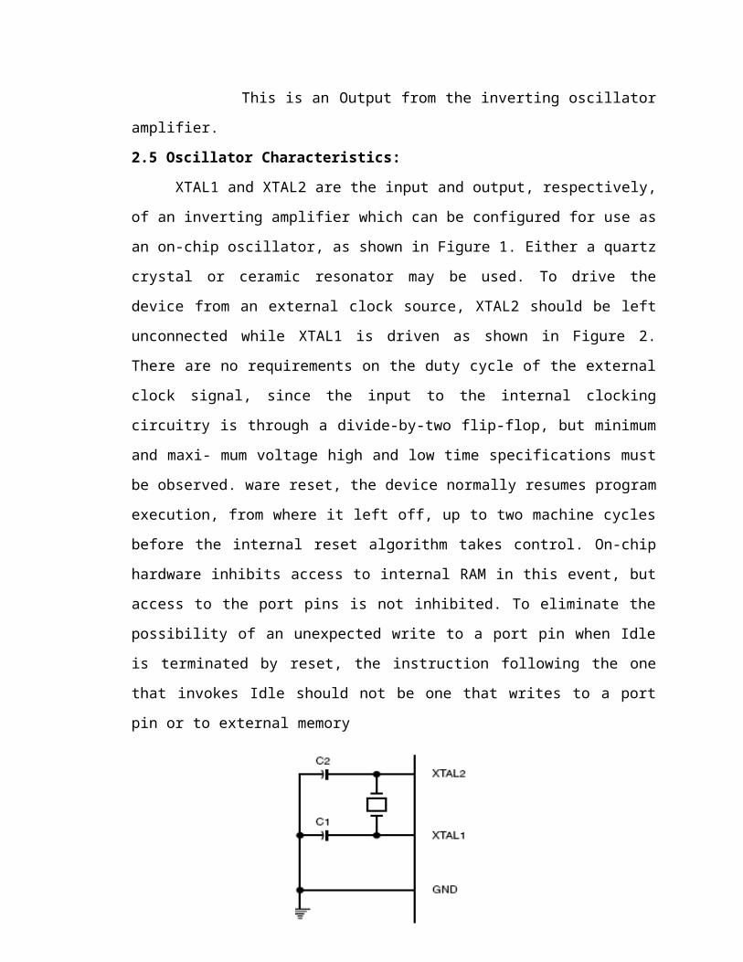
2.5 Oscillator Characteristics:
XTAL1 and XTAL2 are the input and output, respectively, of an inverting
amplifier which can be configured for use as an on-chip oscillator, as shown in Figure 1.
Either a quartz crystal or ceramic resonator may be used. To drive the device from an
external clock source, XTAL2 should be left unconnected while XTAL1 is driven as
shown in Figure 2. There are no requirements on the duty cycle of the external clock
signal, since the input to the internal clocking circuitry is through a divide-by-two flip-
flop, but minimum and maxi- mum voltage high and low time specifications must be
observed. ware reset, the device normally resumes program execution, from where it left
off, up to two machine cycles before the internal reset algorithm takes control. On-chip
hardware inhibits access to internal RAM in this event, but access to the port pins is not
inhibited. To eliminate the possibility of an unexpected write to a port pin when Idle is
terminated by reset, the instruction following the one that invokes Idle should not be one
that writes to a port pin or to external memory
Figure 2.2: Oscillator Connection
CHAPTER-3
HARDWARE REQUIREMENTS
The hardware requirements are as listed below:
Power supply
Reset Circuitry
MAX 232
Relay Circuit
LCD(Liquid Crystal Display)
AT89S51 Micro controller
RFID module
GSM module
3.1 General Components Description
3.1.1 Resistors
A Resistor is a heat-dissipating element and in the electronic circuits it is mostly
used for either controlling the current in the circuit or developing a voltage drop across it,
which could be utilized for many applications. There are various types of resistors, which
can be classified according to a number of factors depending upon:
Material used for fabrication
Wattage and physical size
Intended application
Ambient temperature rating
Cost
Basically the resistor can be split in to the following four parts from the construction
viewpoint.
Base
Resistance element
Terminals
Protective means.
The following characteristics are inherent in all resistors and may be controlled by design
considerations and choice of material i.e. Temperature co–efficient of resistance, Voltage
co–efficient of resistance, high frequency characteristics, power rating, tolerance &
voltage rating of resistors. Resistors may be classified as
a. Fixed
b. Semi variable
c. Variable resistor.
3.1.2 Capacitors
Capacitor is an energy storing component & it allows ac component and blocks
the dc component.
The fundamental relation for the capacitance between two flat plates separated by a
dielectric material is given by:-
C=0.08854KA/D
Where C= capacitance in pf.
K= dielectric constant
A=Area per plate in square cm.
D=Distance between two plates in cm
Design of capacitor depends on the proper dielectric material with particular type of
application. The dielectric material used for capacitors may be grouped in various classes
like Mica, Glass, air, ceramic, paper, Aluminum, electrolyte etc. The value of capacitance
never remains constant. It changes with temperature, frequency and aging.
3.1.3 Diodes
Diode is a two terminal device consisting of a P-N junction formed either of Ge or
Si crystal.
+ - The P and N type regions are referred to as anode and cathode respectively.
Commercially available diodes usually have some means to indicate which lead is P and
which lead is N.
3.1.4 Transistor A transistor consists of two junctions formed by sandwiching either p-type or n-
type semiconductor between a pair of opposite types.
There are two types of transistors namely: -
1. n-p-n transistor
2. p-n-p transistor
An n-p-n transistor is composed of two n-type semiconductors separated by a thin
section of p type. However a p-n-p transistor is formed by two p sections separated by a
thin section of n-type. In each type of transistor the following points may be noted.
(NPN) (PNP)
A transistor raises the strength of a weak signal and thus acts as an amplifier. The
weak signal is applied between emitter base junction and output is taken across the load
Rc connected in the collector circuit (in common emitter configuration). In order to
achieve faithful amplification, the input circuit should always remain forward biased. To
do so, a dc voltage is applied in the input in addition to the signal.
Transistor may be used in different configuration like CB (common base) & CC
(common collector) according to requirements of amplifier (impedance matching, buffer
amplifier etc.).
3.1.5 LED (Light Emitting Diode)
As its name implies it is a diode, which emits light when forward biased. Charge
carrier recombination takes place when electrons from the N-side cross the junction and
recombine with the holes on the P side. Electrons are in the higher conduction band on
the N side whereas holes are in the lower valence band on the P side. During
recombination, some of the energy is given up in the form of heat and light. In the case of
semiconductor materials like Gallium arsenide (GaAs), Gallium phoshide (Gap) and
Gallium arsenide phoshide (GaAsP) a greater percentage of energy is released during
recombination and is given out in the form of light. LED emits no light when junction is
reverse biased.
3.1.6 Transformer
Definition
The transformer is a static electro-magnetic device that transforms one alternating
voltage (current) into another voltage (current). However, power remains the some during
the transformation. Transformers play a major role in the transmission and distribution of
ac power.
Principle
Transformer works on the principle of mutual induction. A transformer consists of
laminated magnetic core forming the magnetic frame. Primary and secondary coils are
wound upon the two cores of the magnetic frame, linked by the common magnetic flux.
When an alternating voltage is applied across the primary coil, a current flows in the
primary coil producing magnetic flux in the transformer core. This flux induces voltage
in secondary coil. Transformers are classified as: -
(a) Based on position of the windings with respect to core i.e.
(1) Core type transformer
(2) Shell type transformer
(b) Transformation ratio:
(1) Step up transformer
(2) Step down transformer
(c) Core & shell types: Transformer is simplest electrical machine, which consists of
windings on the laminated magnetic core.
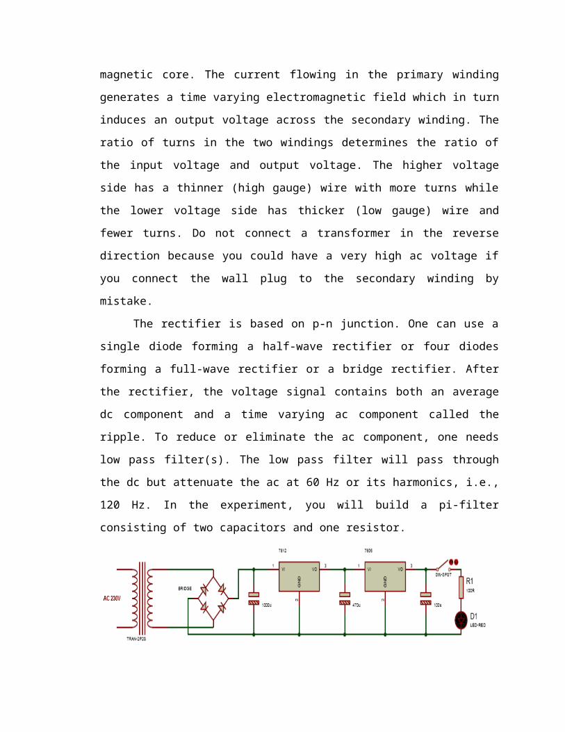
3.2 Power supply
DC power supply exists in every electronic box whether it is a computer, tv, or
equipment in the laboratory. The power supply consists of ac voltage transformer, diode
rectifier, ripple filter, and voltage regulator. The transformer is an ac device. It has two
coil windings, the primary and the secondary, around a common magnetic core. The
current flowing in the primary winding generates a time varying electromagnetic field
which in turn induces an output voltage across the secondary winding. The ratio of turns
in the two windings determines the ratio of the input voltage and output voltage. The
higher voltage side has a thinner (high gauge) wire with more turns while the lower
voltage side has thicker (low gauge) wire and fewer turns. Do not connect a transformer
in the reverse direction because you could have a very high ac voltage if you connect the
wall plug to the secondary winding by mistake.

The rectifier is based on p-n junction. One can use a single diode forming a half-
wave rectifier or four diodes forming a full-wave rectifier or a bridge rectifier. After the
rectifier, the voltage signal contains both an average dc component and a time varying ac
component called the ripple. To reduce or eliminate the ac component, one needs low
pass filter(s). The low pass filter will pass through the dc but attenuate the ac at 60 Hz or
its harmonics, i.e., 120 Hz. In the experiment, you will build a pi-filter consisting of two
capacitors and one resistor.
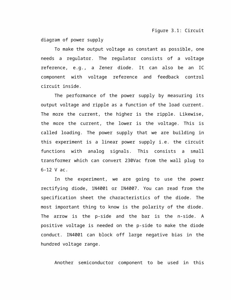
Figure 3.1: Circuit diagram of power supply
To make the output voltage as constant as possible, one needs a regulator. The
regulator consists of a voltage reference, e.g., a Zener diode. It can also be an IC
component with voltage reference and feedback control circuit inside.
The performance of the power supply by measuring its output voltage and ripple
as a function of the load current. The more the current, the higher is the ripple. Likewise,
the more the current, the lower is the voltage. This is called loading. The power supply
that we are building in this experiment is a linear power supply i.e. the circuit functions
with analog signals. This consists a small transformer which can convert 230Vac from
the wall plug to 6-12 V ac.
In the experiment, we are going to use the power rectifying diode, 1N4001 or
IN4007. You can read from the specification sheet the characteristics of the diode. The
most important thing to know is the polarity of the diode. The arrow is the p-side and the
bar is the n-side. A positive voltage is needed on the p-side to make the diode conduct.
IN4001 can block off large negative bias in the hundred voltage range.
Another semiconductor component to be used in this experiment is a voltage
regulator, 7805. “78” indicates that it is a regulator for positive voltage. There is a

corresponding “79” model for negative voltage. “05” indicates that it has an output of 5
V. 7805 is an integrated circuit. 7812 is also the operational amplifier, the design
engineer of the IC has optimized the circuit. Use it as a nearly ideal power supply.
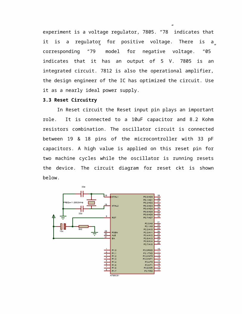
3.3 Reset Circuitry
In Reset circuit the Reset input pin plays an important role. It is connected to a
10uF capacitor and 8.2 Kohm resistors combination. The oscillator circuit is connected
between 19 & 18 pins of the microcontroller with 33 pF capacitors. A high value is
applied on this reset pin for two machine cycles while the oscillator is running resets the
device. The circuit diagram for reset ckt is shown below.
Figure 3.2: Circuit Diagram of Reset Circuit
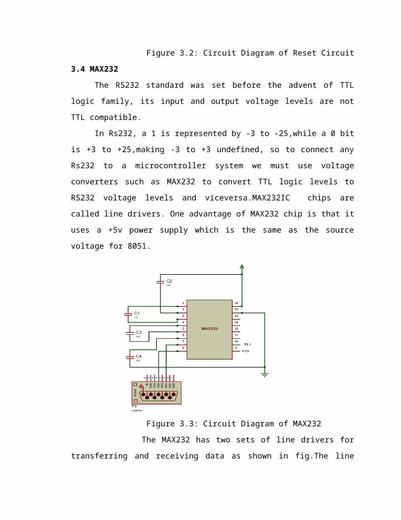
3.4 MAX232
The RS232 standard was set before the advent of TTL logic family, its input and
output voltage levels are not TTL compatible.
In Rs232, a 1 is represented by -3 to -25,while a 0 bit is +3 to +25,making -3 to
+3 undefined, so to connect any Rs232 to a microcontroller system we must use voltage
converters such as MAX232 to convert TTL logic levels to RS232 voltage levels and
viceversa.MAX232IC chips are called line drivers. One advantage of MAX232 chip is
that it uses a +5v power supply which is the same as the source voltage for 8051.
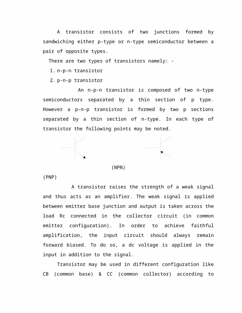
Figure 3.3: Circuit Diagram of MAX232
The MAX232 has two sets of line drivers for transferring and receiving data as
shown in fig.The line drivers used for TxD are called T1 and T2, while the line drivers
for RxD are designated as R1 and R2.In many applications only one of each is used. In
this IC T1 line driver has a designation of T1in and T1out on pin numbers 11 and 14. The
T1in pin is the TTL side and is connected to TxD of the microcontroller, while T1out is
the RS232 side that is connected to RxD pin of the RS232 DB connector. The R1 line
driner has a designation of R1in and r1out on pin numbers 13 and 12 respectively. The
R1in pin is the Rs232 side that is connected to TxD pin of the RS232 DB connector, and
R1out is the TTl side that is connected to the RxD pin of the microcontroller.
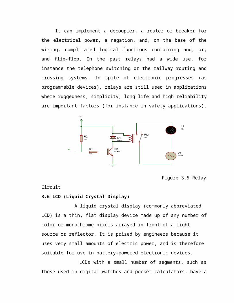
3.5 Relay Circuit The first relay was invented by Joseph Henry in 1835. The name relay derives
from the French noun relays that indicate the horse exchange place of the postman.
Generally a relay is an electrical hardware device having an input and output gate. The
output gate consists in one or more electrical contacts that switch when the input gate is
electrically excited.
Figure 3.4 Relay
It can implement a decoupler, a router or breaker for the electrical power, a
negation, and, on the base of the wiring, complicated logical functions containing and, or,
and flip-flop. In the past relays had a wide use, for instance the telephone switching or the
railway routing and crossing systems. In spite of electronic progresses (as programmable
devices), relays are still used in applications where ruggedness, simplicity, long life and
high reliability are important factors (for instance in safety applications).
Figure 3.5 Relay Circuit
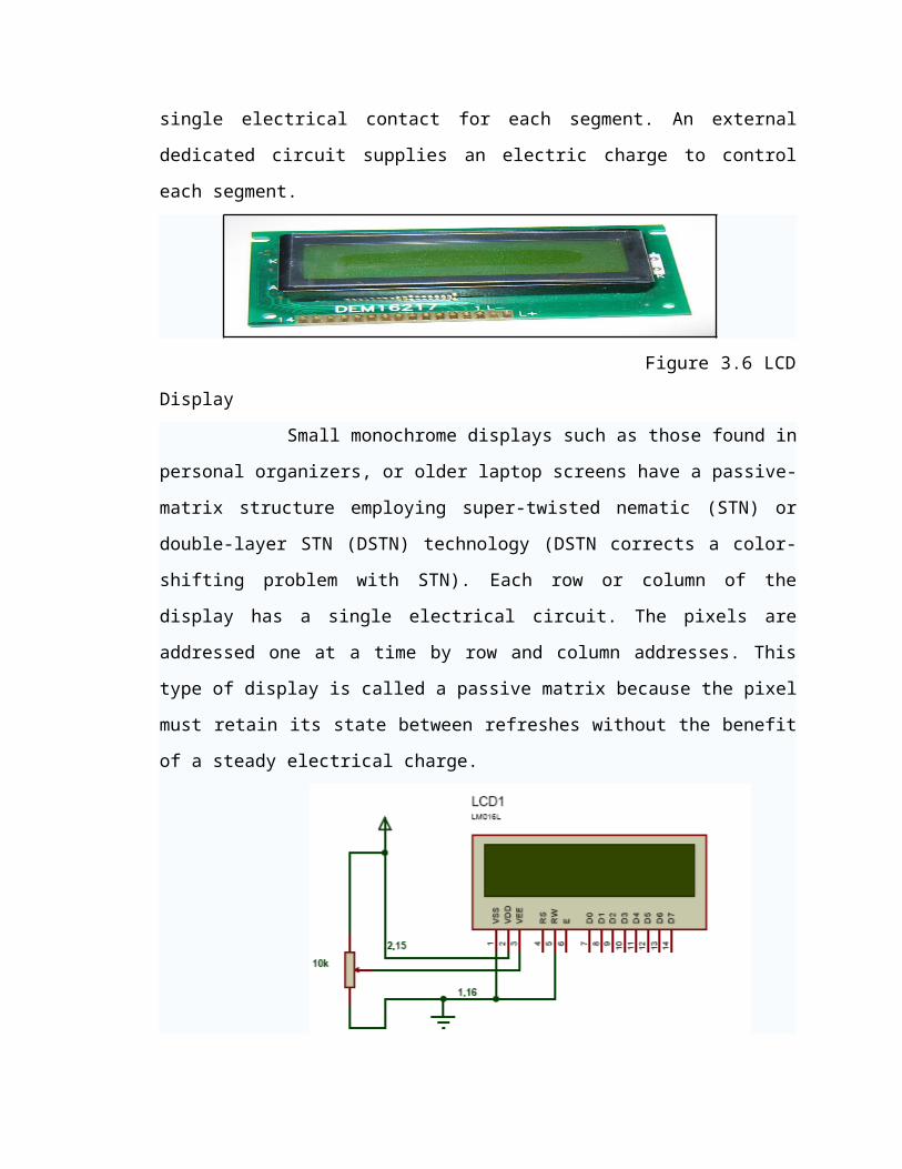
3.6 LCD (Liquid Crystal Display)
A liquid crystal display (commonly abbreviated LCD) is a thin, flat display device
made up of any number of color or monochrome pixels arrayed in front of a light source
or reflector. It is prized by engineers because it uses very small amounts of electric
power, and is therefore suitable for use in battery-powered electronic devices.
LCDs with a small number of segments, such as those used in digital watches and
pocket calculators, have a single electrical contact for each segment. An external
dedicated circuit supplies an electric charge to control each segment.
Figure 3.6 LCD Display
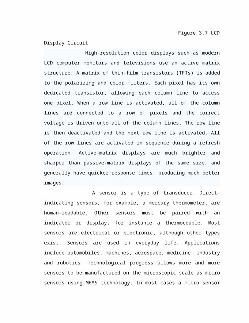
Small monochrome displays such as those found in personal organizers, or older
laptop screens have a passive-matrix structure employing super-twisted nematic (STN) or
double-layer STN (DSTN) technology (DSTN corrects a color-shifting problem with
STN). Each row or column of the display has a single electrical circuit. The pixels are
addressed one at a time by row and column addresses. This type of display is called a
passive matrix because the pixel must retain its state between refreshes without the
benefit of a steady electrical charge.
Figure 3.7 LCD Display Circuit
High-resolution color displays such as modern LCD computer monitors and
televisions use an active matrix structure. A matrix of thin-film transistors (TFTs) is
added to the polarizing and color filters. Each pixel has its own dedicated transistor,
allowing each column line to access one pixel. When a row line is activated, all of the
column lines are connected to a row of pixels and the correct voltage is driven onto all of
the column lines. The row line is then deactivated and the next row line is activated. All
of the row lines are activated in sequence during a refresh operation. Active-matrix
displays are much brighter and sharper than passive-matrix displays of the same size, and
generally have quicker response times, producing much better images.
A sensor is a type of transducer. Direct-indicating sensors, for example, a mercury
thermometer, are human-readable. Other sensors must be paired with an indicator or
display, for instance a thermocouple. Most sensors are electrical or electronic, although
other types exist. Sensors are used in everyday life. Applications include automobiles,
machines, aerospace, medicine, industry and robotics. Technological progress allows
more and more sensors to be manufactured on the microscopic scale as micro sensors
using MEMS technology. In most cases a micro sensor reaches a significantly higher
speed and sensitivity compared with macroscopic approaches. 3.6.1 Features of LCD
5 x 8 dots with cursor
Built-in controller (KS 0066 or Equivalent)
+ 5V power supply (Also available for +3V)
1/16 duty cycle
B/L to be driven by pin 1, pin 2 or pin 15, pin 16 or A.K (LED)
3.6.2 Specifications of LCD
Important factors to consider when evaluating an LCD monitor include:-
Resolution: unlike CRT monitors, LCD monitors have a native-supported
resolution for best display effect.
Dot pitch: The granularity of LCD pixels. The smaller, the better.
viewable size: The length of diagonal of a LCD panel
response time (sync rate)
matrix type (passive or active)
viewing angle
Colour support: How many types of colours are supported.
Brightness: The amount of light emitted from the display.
contrast ratio
Aspect ratio: 4 by 3, 16 by 9, 16 by 10, etc.
CHAPTER-4
KIT MODULES4.1 GSM Module
4.1.1 Introduction To GSM:
GSM (Global System for Mobile communication) is a digital mobile telephone
system that is widely used in Europe and other parts of the world. GSM uses a variation
of Time Division Multiple Access (TDMA) and is the most widely used of the three
digital wireless telephone technologies (TDMA, GSM, and CDMA). GSM digitizes and
compresses data, then sends it down a channel with two other streams of user data, each
in its own time slot. It operates at either the 900 MHz or 1,800 MHz frequency band.
GSM is the de facto wireless telephone standard in Europe. GSM has over one
billion users worldwide and is available in 190 countries. Since many GSM network
operators have roaming agreements with foreign operators, users can often continue to
use their Features.
4.1.2 Features:
International roaming
Open architecture
High degree of flexibility
Easy installation
Interoperation with ISDN (Integrated Services Digital Networks), CSPDN
(Circuit-Switched Public Data Network), PSPDN (Packed- Switched Public Data
Network), and PSTN (Public-Switched Telephone Network)
High-quality signal and link integrity
High spectral efficiency
Low-cost infrastructure
Low-cost, small terminals
Security features
4.1.3 GSM Services
GSM services are grouped into three categories:
1. Teleservices (TS)
2. Subscriber services (BS)
3. Supplementary services (SS) TS cover, in essence, telephony, BS encompass basically
data transmission, and SS are the value-added features.
Teleservices:
Regular telephony, emergency calls, and voice messaging are within TS.
Telephony, the old bidirectional speech calls, is certainly the most popular of all services.
An emergency call is a feature that allows the mobile subscriber to contact a nearby
emergency service, such as police, by dialing a unique number. Voice messaging permits
a message to be stored within the voice mailbox of the called party either because the
called party is not reachable or because the calling party chooses to do so.
Subscriber Services:
There are two basic types of services offered through GSM: telephony (also
referred to as teleservices and data (also referred to as bearer services). Telephony
services are mainly voice services that provide subscribers with the complete capability
(including necessary terminal equipment) to communicate with other subscribers. Data
services provide the capacity necessary to transmit appropriate data signals between two
access points creating an interface to the network.
Supplementary Services
GSM supports a comprehensive set of supplementary services that can
complement and support both telephony and data services. Supplementary services are
defined by GSM and are characterized as revenue-generating features. A partial listing of
supplementary services follows.
Call Forwarding- This service gives the subscriber the ability to forward
incoming calls to another number if the called mobile unit is not reachable. if it is
busy, if there is no reply, or if call forwarding is allowed unconditionally.
Barring of Outgoing Calls- This service makes it possible for a mobile
subscriber to prevent all outgoing calls.
Barring of Incoming Calls- This function allows subscriber to prevent incoming
calls. The following two conditions for incoming call barring exist: bearing of all
incoming calls and barring calls when roaming outside the home PLMN.
Advice of Charge (AOC)- The AOC service provides the mobile subscriber with
an estimate of the call charges. There are two types of AOC information: one that
provides the subscriber with an estimate of the bill and that can be used for
immediate charging purposes. AOC for data calls is provided on the basis of time
measurements.
Call Hold- This service enables the subscriber to interrupt an ongoing call and
then subsequently reestablish the call. The call hold service is only applicable to
normal telephony.
Call Waiting- this service enables the mobile subscriber to be notified of an
incoming call during a conversation. The subscriber can answer, reject, or ignore
the incoming call. Call waiting is applicable to all GSM telecommunications
services using a circuit-switched connection.
Multiparty service- The multiparty service enables a mobile subscriber to
establish a multiparty conversation-that is, a simultaneous conversation between
three and six subscribers. This service is only applicable to normal telephony.
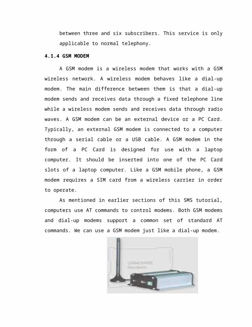
4.1.4 GSM MODEM
A GSM modem is a wireless modem that works with a GSM wireless network. A
wireless modem behaves like a dial-up modem. The main difference between them is that
a dial-up modem sends and receives data through a fixed telephone line while a wireless
modem sends and receives data through radio waves. A GSM modem can be an external
device or a PC Card. Typically, an external GSM modem is connected to a computer
through a serial cable or a USB cable. A GSM modem in the form of a PC Card is
designed for use with a laptop computer. It should be inserted into one of the PC Card
slots of a laptop computer. Like a GSM mobile phone, a GSM modem requires a SIM
card from a wireless carrier in order to operate.
As mentioned in earlier sections of this SMS tutorial, computers use AT
commands to control modems. Both GSM modems and dial-up modems support a
common set of standard AT commands. We can use a GSM modem just like a dial-up
modem.
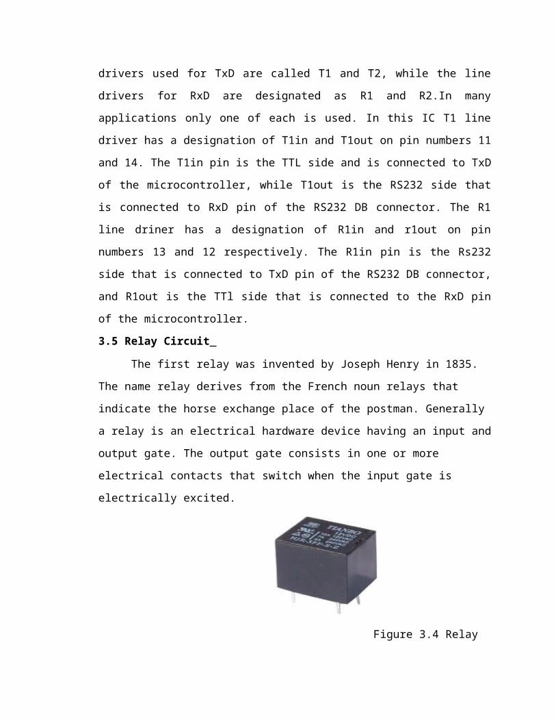
Figure 4.1 GSM Modem
In addition to the standard AT commands, GSM modems support an extended set of
AT commands. These extended AT commands are defined in the GSM standards. With
the extended AT commands, we can do the following things :
Reading, writing and deleting SMS messages.
Sending SMS messages.
Monitoring the signal strength.
Monitoring the charging status and charge level of the battery.
Reading, writing and searching phone book entries.
The number of SMS messages that can be processed by a GSM modem per minute is
very low i.e., only about six to ten SMS messages per minute.
4.1.5 GSM AT Commands
Some advanced GSM modems like WaveCom and Multitech, support the SMS
text mode. This mode allows you to send and receive SMS messages using AT
commands, without the need to decode the binary PDU field of the SMS first. This is
done by the GSM modem.
To check if GSM modem supports this text mode, the following command is used:
a) Setting up the modem
If the modem contains a SIM card with is secured with a PIN code, we have to
enter this pin code first:
AT+CPIN="0000" <ENTER> (replace 0000 with your PIN code)
In most cases you have only 3 attemps to set the correct PIN code. After setting
the PIN code, wait some seconds before issueing the next command to give the modem
some time to register with the GSM network.
In order to send a SMS, the modem has to be put in SMS text mode first using the
following command:
AT+CMGF=1 <ENTER>
If the modem responds with error, either the modem does not support SMS text
mode, or the SIM card is not ready. In this case please check that the SIM card is inserted
and the pin code is entered. You can also turn on extended error reports by using the
following command:
AT+CMEE=1 <ENTER>
Instead of just an "ERROR" the modem will now respond with "+CMS ERROR:
xxx" or "+CME ERROR: xxx".
b) Sending the message
To send the SMS message, type the following command:
AT+CMGS="+7382117825" <ENTER>
Place the above phone number with your own cell phone number to which the
delivery message will come. The modem will respond according to that number.
You can now type the message text and send the message using the <CTRL>-<Z>
key combination.
Hello World! <CTRL-Z>
After some seconds the modem will respond with the message ID of the message,
indicating that the message was sent correctly.
c) Selecting the preferred message storage
A GSM phone or modem receives messages automatically. Basically you are just
retrieving the messages from the memory of the device or SIM card. To select the
message storage used to read the messages either from SIM memory or Buffer memory,
use the "AT+CPMS" command. 7
AT+CPMS="SM" <ENTER>
Read SMS messages from the SIM card. This storage is supported on every
GSM phone, because a SIM card should always be present. Usually a SIM card can
store up to 15 messages.
AT+CPMS="BM" <ENTER>
This storage is only used to read stored incoming cell broadcast messages.
It stores these cell broadcast messages into buffer memory temporarily. But It is
normally not used to store SMS messages.
d) Listing the messages
Once you have successfully set the messages storage, you can list the messages
available using the list command:
AT+CMGL="ALL" <ENTER>
This command is used to set the messages in gist list. So in this command
"ALL" has to be send in uppercase on some modems. The modem will respond
with a list of decoded SMS messages in a list format.
e) Reading a message
To list a single message, you have to use the read command. Use the list
command first, so you know the indexes of the messages in the storage. For
instance, to read the message on memory location '2' use:
AT+CMGR=2 <ENTER>
This command is used to read the message on memory location 2.The modem
will list the single message.
AT+CMGR= "REC READ"<ENTER>
The output is stored as Test message 2.Then type OK.
The status of the message is now "REC_READ" instead of "REC_UNREAD"
because we read the message.
f) Deleting a message
After reading a message, the memory becomes free by deleting the message
from the storage. For instance, to delete the message on memory location '2' use:
AT+CMGD=2 <ENTER>
By using this command, the modem will delete the single message from
memory location2.
g) Receiving SMS messages
This mode allows you to receive SMS messages using AT commands, without
the need to decode the binary PDU field of the SMS first. To send the commands
you can use a terminal program, for instance Hyper terminal.
To check if your modem supports this text mode, you can try the following
command.
AT+CMGF=1 <ENTER>
If the modem responds with "OK" this mode is supported. Please note that
using this mode it is only possible to send simple text messages. It is not possible
to send multipart, Unicode, data and other types of messages.
4.2 RFID Module
4.2.1 Introduction
RFID, its application, standardisation, and innovation are constantly changing.
Its adoption is still relatively new and hence there are many features of the
technology that are not well understood by the others.
Developments in RFID technology continue to yield larger memory capacities,
wider reading ranges, and faster processing. It’s highly unlikely that the technology
will ultimately replace bar code - even with the inevitable reduction in raw
materials coupled with economies of scale, the integrated circuit in an RF tag will
never be as cost-effective as a bar code label. However, RFID will continue to
grow in its established niches where bar code or other optical technologies aren’t
effective.
This document tries to set out the basic information about RFID in a simple
format that can be understood by everyone. AIM’s purpose is to provide education
on RFID and hence increase the use of the technology.
A moment’s thought about radio broadcasts or mobile telephones and one can
readily appreciate the benefits of wireless communication. RFID is an area of
automatic identification that has quietly been gaining momentum in recent years
and is now being seen as a radical means of enhancing data handling processes,
complimentary in many ways to other data capture technologies such bar coding. A
range of devices and associated systems are available to satisfy an even broader
range of applications. Just as one need not know the technicalities of a mobile
phone or personal computer to use it, it is not necessary to know the technicalities
to understand the principles, considerations and potential for using RFID.
4.2.2 What is RFID?
The object of any RFID system is to carry data in suitable transponders,
generally known as tags, and to retrieve data, by machine-readable means, at a
suitable time and place to satisfy particular application needs. Data within a tag
may provide identification for an item in manufacture, goods in transit, a location,
the identity of a vehicle, an animal or individual.
For example, the colour of paint for a car body entering a paint spray area on
the production line, the set-up instructions for a flexible manufacturing cell or the
manifest to accompany a shipment of goods.
A system requires, in addition to tags, a means of reading or interrogating the
tags and some means of communicating the data to a host computer or information
management system. A system will also include a facility for entering or
programming data into the tags, if this is not undertaken at source by the
manufacturer. Quite often an antenna is distinguished as if it were a separate part of
an RFID system.
To understand and appreciate the capabilities of RFID systems it is necessary
to consider their constituent parts. It is also necessary to consider the data flow
requirements that influence the choice of systems and the practicalities of
communicating across the air interface. By considering the system components and
their function within the data flow chain it is possible to grasp most of the
important issues that influence the effective application of RFID.
4.2.3 Wireless communication and the air interface
Communication of data between tags and a reader is by wireless
communication. Two methods distinguish and categorise RFID systems, one based
upon close proximity electromagnetic or inductive coupling and one based upon
propagating electromagnetic waves. Coupling is via ‘antenna’ structures forming
an integral feature in both tags and readers. While the term antenna is generally
considered more appropriate for propagating systems it is also loosely applied to
inductive systems.
Transmitting data is subject to the vagaries and influences of the media or
channels through which the data has to pass, including the air interface. Noise,
interference and distortion are the sources of data corruption that arise in practical
communication channels that must be guarded against in seeking to achieve error
free data recovery. The nature of the data communication processes, being
asynchronous or unsynchronised in nature.
To transfer data efficiently via the air interface or space that separates the
two communicating components requires the data to be superimposed upon a
sinusoidal or carrier wave. This process of superimposition is referred to as
modulation. They are essentially based upon changing the value of one of the
primary features of an alternating sinusoidal source, its amplitude, frequency or
phase in accordance with the data carrying bit stream. On this basis one can
distinguish amplitude shift keying (ASK), frequency shift keying (FSK) and phase
shift keying (PSK).
4.2.4 Carrier frequencies
The approach that is generally adopted for radio frequency communication
channels is to separate on the basis of frequency allocation.
Three frequency ranges are generally distinguished for RFID systems, low,
intermediate (medium) and high. The following table summarises these three
frequency ranges, along with the typical system characteristics and examples of
major areas of application.
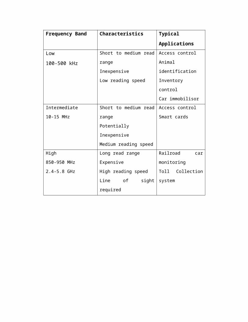
Table 2.2: Frequency Bands and Applications
4.2.5 Data transfer rate and bandwidth
Choice of field or carrier wave frequency is of primary importance in
determining data transfer rates. In practical terms the rate of data transfer is
influenced primarily by the frequency of the carrier wave or varying field used to
carry the data between the tag and its reader. Generally, higher the frequency then
higher the data transfer or throughput rates that can be achieved. This is intimately
linked to bandwidth or range available within the frequency spectrum for the
communication process.
Frequency Band Characteristics Typical Applications
Low
100-500 kHz
Short to medium read range
Inexpensive
Low reading speed
Access control
Animal identification
Inventory control
Car immobilisor
Intermediate
10-15 MHz
Short to medium read range
Potentially Inexpensive
Medium reading speed
Access control
Smart cards
High
850-950 MHz
2.4-5.8 GHz
Long read range
Expensive
High reading speed
Line of sight required
Railroad car monitoring
Toll Collection system
The channel bandwidth needs to be at least twice the bit rate required for the
application. Using the 2.4 - 2.5 GHz spread spectrum band, for example, 2
megabits per second data rates may be achieved, with added noise immunity
provided by the spread spectrum modulation approach. Spread spectrum apart,
increasing the bandwidth allows an increase noise level and a reduction in signal-
to-noise ratio.
4.2.6 Range and Power Levels
The range that can be achieved in an RFID system is essentially determined
by:
The power available at the reader/interrogator to communicate with the
tag(s)
The power available within the tag to respond
The environmental conditions and structures, the former being more
significant at higher frequencies including signal to noise ratio
The antenna design will determine the shape of the field or propagation wave
delivered, so that range will also be influenced by the angle subtended between the
tag and antenna.
In space free of any obstructions or absorption mechanisms the strength of the
field reduces in inverse proportion to the square of the distance. For a wave
propagating through a region in which reflections can arise from the ground and
from obstacles, the reduction in strength can vary quite considerable, in some cases
as an inverse fourth power of the distance. Where different paths arise in this way
the phenomenon is known as “multi-path attenuation”.
At higher frequencies absorption due to the presence of moisture can further
influence range. It is therefore important in many applications to determine how
the environment, internal or external, can influence the range of communication.
In some systems the reader constitutes a receiver and is separate from the
interrogation source or transmitter, particularly if the ‘up-link’ (from transmitter-to-
tag) carrier is different from the ‘down-link’ (from tag-to-reader).
While 100 - 500mW are values often quoted for RFID systems, actual values
should be confirmed with the appropriate regulatory authorities.
4.2.7 RFID System Components
Figure 4.2 Components of RFID system
a) Transponder
The word transponder, derived from TRANSmitter/resPONDER, reveals the
function of the device. The tag responds to a transmitted or communicated request
for the data it carries, the mode of communication between the reader and the tag
being by wireless means across the space or air interface between the two.
Generally transponders are fabricated as low power integrated circuits suitable
for interfacing to external coils, or utilising "coil-on-chip" technology, for data
transfer and power generation (passive mode).
Basic features of an RFID transponder:
The transponder memory may comprise read-only (ROM), random access
(RAM) and non-volatile programmable memory for data storage depending upon
the type of device. The ROM-based memory is used to accommodate security data
and the transponder operating system instructions which, in conjunction with the
processor. The RAM-based memory is used to facilitate temporary data storage
during transponder interrogation and response.
The non-volatile programmable memory may take various forms, electrically
erasable programmable read only memory (EEPROM) being typical. It is used to
store the transponder data and needs to be non-volatile to ensure that the data is
retained when the device is in its quiescent or power-saving "sleep" state.
b) AntennaTag
The transponder antenna is the means by which the device senses the
interrogating field and, where appropriate, the programming field and also serves
as the means of transmitting the transponder response to interrogation.
A number of features, in addition to carrier frequency, characterise RFID
transponders and form the basis of device specifications, including:
Means by which a transponder is powered
Data carrying options
Data read rates
Programming options
Physical form & costs
c) The Reader/Interrogator
The reader/interrogators can differ quite considerably in complexity,
depending upon the type of tags being supported and the functions to be fulfilled.
However, the overall function is to provide the means of communicating with the
tags and facilitating data transfer. Functions performed by the reader may include
signal conditioning, parity error checking and correction. Once the signal from a
transponder has been correctly received and decoded, algorithms may be applied to
decide whether the signal is a repeat transmission, and may then instruct the
transponder to transmit.
This is known as the “Command Response Protocol” and is used to
overcome the problem of reading multiple tags in a short space of time.
Using interrogators in this way is sometimes referred to as “Hands Down Polling”.
An alternative, more secure, but slower tag polling technique is called “Hands Up
Polling” which involves the interrogator looking for tags with specific identities,
and interrogating them in turn.
d) RF Transponder Programmers
Transponder programmers are the means by which data is delivered to write
once, read many (WORM) and read/write tags. Programming is generally carried
out off-line, at the beginning of a batch production run.
For some systems re-programming may be carried out on-line, particularly
if it is being used as an interactive portable data file within a production
environment. Data may need to be recorded during each process. Removing the
transponder at the end of each process to read the previous process data, and to
programme the new data, would naturally increase process time and would detract
substantially from the intended flexibility of the application. By combining the
functions of a reader/interrogator and a programmer, data may be appended or
altered in the transponder.
The range over which the programming can be achieved is generally less
than the read range and in some systems near contact positioning is required.
Programmers are also generally designed to handle a single tag at a time.
4.2.8 RFID System Categories
RFID systems may be grouped into four categories:
1. EAS (Electronic Article Surveillance) systems
2. Portable Data Capture systems
3. Networked systems
4. Positioning systems
Electronic Article Surveillance systems are typically a one bit system used to
sense the presence/absence of an item. The large use for this technology is in retail
stores where each item is tagged and a large antenna readers are placed at each exit
of the store to detect unauthorised removal of the item (theft).
Portable data capture systems are characterised by the use of portable data
terminals with integral RFID readers and are used in applications where a high
degree of variability in sourcing required data from tagged items may be exhibited.
The hand-held readers/portable data terminals capture data which is then either
transmitted directly to a host information management system via a radio
frequency data communication (RFDC) link or held for delivery by line-linkage to
the host on a batch processing basis.
Networked systems applications can generally be characterised by fixed
position readers deployed within a given site and connected directly to a networked
information management system. The transponders are positioned on moving or
moveable items, or people, depending upon application.
Positioning systems use transponders to facilitate automated location and
navigation support for guided vehicles. Readers are positioned on the vehicles and
linked to an on-board computer and RFDC link to the host information
management system. The transponders are embedded in the floor of the operating
environment and programmed with appropriate identification and location data.
The reader antenna is usually located beneath the vehicle to allow closer proximity
to the embedded transponders.
4.2.9 Areas of Application for RFID
Potential applications for RFID may be identified in virtually every sector of
industry, commerce and services where data is to be collected. The attributes of
RFID are complimentary to other data capture technologies and thus able to satisfy
particular application requirements that cannot be adequately accommodate by
alternative technologies. Principal areas of application for RFID that can be
currently identified include:
Transportation and logistics
Manufacturing and Processing
Security
A range of miscellaneous applications may also be distinguished, some of which
are steadily growing in terms of application numbers. They include:
Animal tagging
Waste management
Time and attendance
Postal tracking
Airline baggage reconciliation
Road toll management
As standards emerge, technology develops still further, and costs reduce
considerable growth in terms of application numbers and new areas of application
may be expected.
Some of the more prominent specific applications include:
Electronic article surveillance - clothing retail outlets being typical.
Protection of valuable equipment against theft, unauthorised removal or
asset management.
Controlled access to vehicles, parking areas and fuel facilities - depot
facilities being typical.
Automated toll collection for roads and bridges - since the 1980s, electronic
Road-Pricing (ERP) systems have been used in Hong Kong.
Controlled access of personnel to secure or hazardous locations.
Time and attendance - to replace conventional “slot card” time keeping
systems.
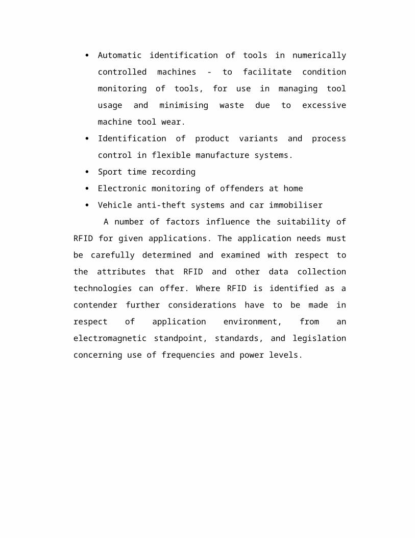
Automatic identification of tools in numerically controlled machines - to
facilitate condition monitoring of tools, for use in managing tool usage and
minimising waste due to excessive machine tool wear.
Identification of product variants and process control in flexible
manufacture systems.
Sport time recording
Electronic monitoring of offenders at home
Vehicle anti-theft systems and car immobiliser
A number of factors influence the suitability of RFID for given applications.
The application needs must be carefully determined and examined with respect to
the attributes that RFID and other data collection technologies can offer. Where
RFID is identified as a contender further considerations have to be made in respect
of application environment, from an electromagnetic standpoint, standards, and
legislation concerning use of frequencies and power levels.
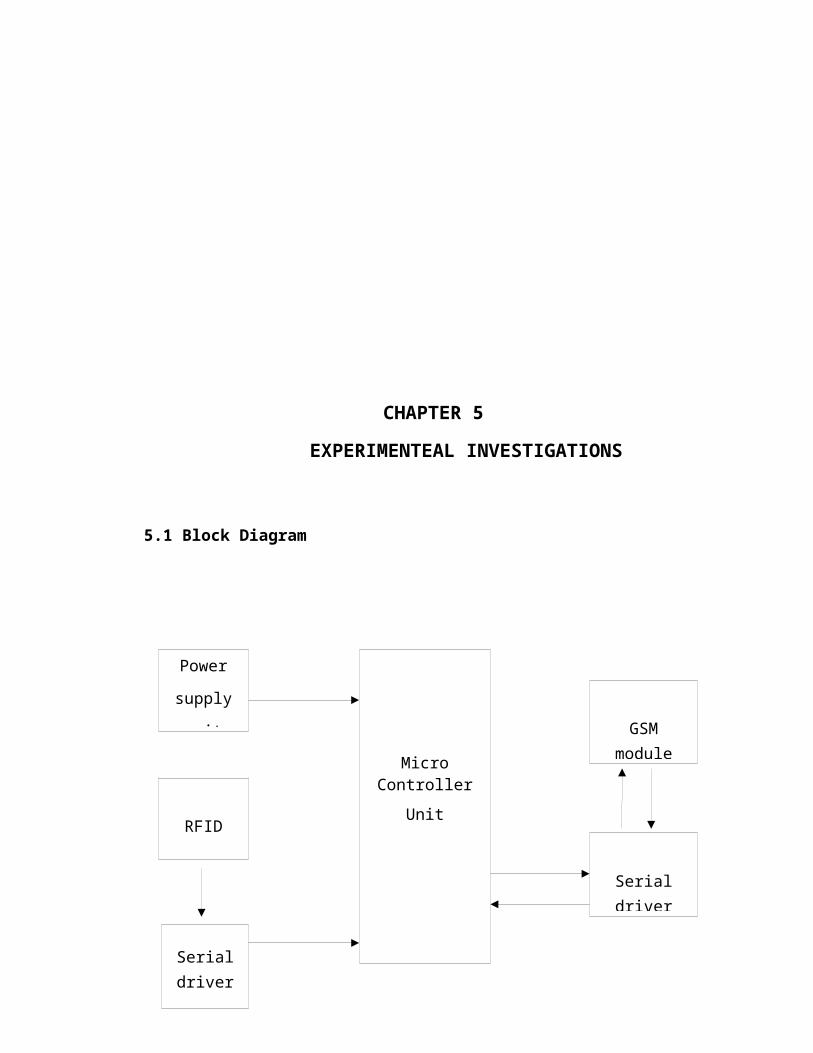
CHAPTER 5
EXPERIMENTEAL INVESTIGATIONS
5.1 Block Diagram
Figure 5.1: Block diagram
Power
supply
unit
RFID
Serial driver
Micro Controller
Unit
GSM module
Serial driver
5.2 Circuit Diagram
Figure 5.2: Total Circuit diagram with Pin Configuration
5.3 Software implementation:
5.3.1 Software Development Tools
In the embedded world there are any numbers of reasons to do your actual
programming work on a system other than the one on which the software will eventually
run. The system that you shift may or may not have a key board, a screen, a disk drive,
and the other peripherals necessary for programming. It may not have enough memory to
run a programming editor, or it may be that nobody has ever written an editor to run on
the particular microprocessor your system uses. Therefore, most programming work for
embedded systems is done on a host, a computer system on which all the programming
tools run. Only after the program has been written, compiled assembled and linked is it
moved to the target, the system that is shipped to customers. Some people use the word
workstation instead of host; the word target is almost universal.
5.3.2 Cross Compilers
Most desktop systems used as hosts come with compilers, assemblers, linkers and
so on for building programs that will run on the host. These tools are called native tools.
The native compiler on a Windows NT system based on an Intel Pentium, for example,
builds programs intended to run on an Intel Pentium. This compiler may possibly be
useful if your target microprocessor is a Pentium, but it is completely useless if your
target microprocessor is something else, say a Motorola 68000 or a MIPS or a Zilog Z80.
These later processors won’t understand binary Pentium instructions. But Pentium
instructions are what the native compiler produces. What you need is a compiler that runs
on your target microprocessor. Such a program is called a cross-compiler.
In an ideal world, if you wrote a program in C or C++ that you could compile on
your native compiler and run on your host, you could run that same source code through
your cross-compiler and have a program that would run on your target. Unfortunately,
this is not true, not even in theory, much less in practice. In theory, a program that
compiles without error on your native compiler should also compile without error on the
cross-compiler. The rules about what constitutes a correctly formed C or C++ program
are well defined. However, in practice we should expect that certain constructions
accepted by one compiler will not be accepted by another. You will not have problems
with if statements or switch statements or do loops; the problems will arise with
functions that you use without declaring, functions that u declare using older styles of
declarations, and so on. The compiler vendors have been working to minimize this
problem, but it has not quite yet gone away.
The fact that your program works on your host machine and compiles cleanly
with your cross-compiler is no assurance that it will work on your target system. The
same problems that haunt every other effort to port C programs from one machine to
another apply. The variables declared as int may be one size on the host and a different
size on the target. Structures may be packed differently on the two machines. Your ability
to access 16-bit and 32-bit entities that reside at odd-numbered addresses may be
different.
Because of this, you should expect a different collection of warnings from your
cross-compiler. For example, if your code casts a void pointer to an int, the native
compiler may know that the two entities are the same size and do not issue a warning.
The cross- compiler, on the other hand, may warn you that ints and void pointers are not
the same size on the target system.
5.3.3 Cross-Assemblers and Tool chains: Another tool that you will need if you must write any of your program in
assembly language is a cross-assembler. As you might imagine from the name, a cross-
assembler is an assembler that runs on your host but produces binary instructions
appropriate for your target. The input to the cross-assembler must be assembly language
for the target. There is no point in expecting that appropriate input for the cross assembler
has any relationship to input for the native assembler.
The output files from each tool become the input files for the next. Because of
this, the tools must be compatible with one another. A set of tools that is compatible in
this way is called a tool chain. Tool chains that run on various hosts and that build
programs for various targets are available from many vendors.
5.3.4 Linker/Locator for embedded software
Although the job of a cross-compiler is much the same as that of a native
compiler-read in a source file and produce an object file suitable for the linker- a linker
for an embedded system must do a number of things differently from a native linker. In
fact, the two programs are different enough that linkers for embedded systems are often
called linker/locator. In this section we will discuss the difference between locators and
native linkers.
4.4 Programming code
#include <reg52.h>#include <string.h>sbit rs=P3^2;sbit rw=P3^3;sbit en=P3^4;sbit relay=P3^5;
void serstr(unsigned char *);void del();void ser(unsigned char);void lcd_ini();void lcdcmd(unsigned char);void lcdstr(unsigned char *);void lcddis(unsigned char);idata unsigned char read[13];code unsigned char card1[]="25001C3B9A98",card2[]="25001C18AE8F";
void main(){unsigned char i;SCON=0x50;TMOD=0x20;TH1=-3;TR1=1;serstr("AT+CMGF=1\r");del();while(RI){RI=0;del();}
lcd_ini();while (1){lcdcmd(0x01);relay=0;lcdstr("Waiting");for (i=0;i<12;i++){ while (!RI); RI=0; read[i]=SBUF;}lcdstr(read);serstr(read);lcdcmd(0xc0);if (!strncmp(card1,read,12)){ relay=1; serstr("AT+CMGS=\"8500068991\"\r"); serstr("Location1"); lcdstr("Location1"); ser(0x1a); for (i=0;i<100;i++) del(); RI=0; while (RI){RI=0;del();del();} serstr("AT+CMGS=\"+918500068991\"\r"); serstr("Location1"); ser(0x1a);}else if (!strncmp(card2,read,12)){ relay=1; serstr("AT+CMGS=\"8500068991\"\r"); serstr("Location2"); lcdstr("Location2"); ser(0x1a); for (i=0;i<100;i++) del(); RI=0; while (RI){RI=0;del();del();}
serstr("AT+CMGS=\"+918500068991\"\r"); serstr("Location2"); ser(0x1a);}
}}
void lcd_ini(){ lcdcmd(0x38); lcdcmd(0x01); lcdcmd(0x06); lcdcmd(0x0e);}
void lcdcmd(unsigned char cmd){ P1=cmd; rs=0; rw=0; en=1; del(); en=0;}
void lcddis(unsigned char dis){ P1=dis; rs=1; rw=0; en=1; del(); en=0;}
void lcdstr(unsigned char *str){ unsigned char i=0; while (str[i]!=0) lcddis(str[i++]);
}
void serstr(unsigned char *str){ unsigned char i=0; while (str[i]!=0) ser(str[i++]);}
void ser(unsigned char tx){ SBUF=tx; while (!TI); TI=0;}
void del(){ unsigned int i=10000; while (i--);}
CHAPTER 6
EXPERIMENTAL RESULTS
6.1 Results
The kit works according to the commands given through SMS from owner mobile
to the mobile in the kit. Each device is allocated with a number, using this numbers we
can control the devices individually. At a time we can control the devices by using the
command ALL. We also get the status of the devices by STATUS command. The
following are the commands
COMMAND DESCRIPTION
1ON The bulb will be ON
2ON The Motor will be ON
3ON The LED will be ON
1OFF The bulb will be OFF
2OFF The Motor will be OFF
3OFF The LED will be OFF
ALL ON All devices are ON
ALL OFF All devices are OFF
STATUS We get status reply
Table 5.1:Commands and their description
The project kit design makes use of 8051 micro controller for interfacing to
various hardware peripherals. Technology today is seeing its heights in all the areas,
especially in the area of Embedded Systems. It is true that every electronic gadget that is
used in daily life right from a PC keyboard to a refrigerator is an Embedded System. This
itself shows how vastly the technology is expanding.
As the time moves the life style of the persons has completely changed and there
is no time for the people for micro management of every issue personally. So, this is the
right time to provide some space to the technology into our lives for monitoring the
issues which requires our personal presence for the things to happen. One among those
issues which require our personal presence is receiving the courier which is sent back if
we are not present at the time the courier boy comes to our house. This may lead to the
delay in receiving the data and in some scenarios it may also lead to tough situations. So
our project aims in providing a very reliable and very user friendly solution to overcome
this kind of problem.
As we know the advancements in the Radio Frequency and GSM technologies
and making use of those existing technologies we can design a device which is capable of
identifying the arrival of courier and forward the same to the receiver and also send an
acknowledgement to the courier office so that they do not require the signature of the
particular person for whom the courier is meant for. The basic idea of the system is to
employ an RF ID tag to the courier and send the identity number to the receivers mobile.
The receiver of the courier will have a letter box which has an RF reader and a dedicated
GSM modem in it. As soon as the courier boy drops the letter in to it the RF reader reads
the identity number of the tag and informs the same to a micro controller and compares it
with the identity number send by the courier office and if both are one and the same then
it sends message to the receiver and also to the courier office about the arrival of the
courier. Using RFID at various intermediate the sender and receiver are also intimated
about the location of the courier package. To design the entire system we require a
microcontroller which acts as a medium of communication between the RF reader and
the GSM modem. The major advantage of this system is the presence of the GSM modem
enables the device to communicate with the receiver no matter where ever he was present
on the globe.
6.2 Photos
CHAPTER 7
DISCUSSION OF RESULTS
7.1 Applications and Limitations
7.1.1 Applications
Home
Industry
Farmers
Street light control
7.1.2 Limitations
Both mobiles should be in coverage area
Only applicable to GSM mobiles
Coding must be changed when the mobile in the kit is replaced
Limited number of devices can be controlled
7.2 Merits and Demerits
7.2.1 Merits
Flexible to operate
Less cost
Manual work is less
At a time we can control all the machines
There is no distance limit
7.2.2 Demerits
No security
Chances of getting wrong status report
Relay specifications must be improved for implementing in industries
Chance of delay in receiving message
CHAPTER 8
SUMMARY, CONCLUSION & RECOMMENDATIONS
Summary
In this project we came to know about L293d driver amplifiers,SMS
technology Serial communication, and implementation of the mobile technology in to
embedded system
This project is very useful because the main application is controlling home appliances
which Is helpful even to the common man.
Conclusion
We can control any device just by sending message to mobile to embedded in
the device from anywhere in the world.
Recommendations
To get message reply if device is not working.
To get message if any voltage fluctuation is occurred.
Message can be reached or replied even if mobile is in out of coverage area, after
sometime.
Access able to only certain numbers
APPENDICES
PROCEDURE TO WORK ON KEIL SOFTWARE
To generate an application in uVision2:
a) Select Project - Open Project: For example, C166\examples\hello\hello.uv2
b) Select Project - Rebuild all target files or Build target
To create our own application in uVision2:
a) Select Project - New Project:
Select a directory and enter project file.
b) Select Project - Select Device:
Select an 8051, 166, or ST10 device
c) Select Project - Targets, Groups, Files:
Add/Files, select Source Group1 and add the source files
d) Select Project - Options:
Set all the tool options (the defaults are typically good
settings for first projects, just add the external memory
devices you are using)
e) Select Project - Rebuild all target files or Build target
To debug an application in uVision2
a) Select Debug - Start/Stop Debug Session
b) Use Step toolbar buttons or enter in Output Window - Command: G, main
c) we may open the Serial Window by pressing the Toolbar
"Serial #1" button
d) Now, we may debug our program with standard options: Step, Go, Break.
REFERENCES
Text books
Progrmming for Embedded systems by - Dreamtech software team.
Embedded system design by - Frank vahid & Tony Givagis.
Progrmming with 8051 microcontroller by - Joseph Mazidi &Mazidi Pearson
Edneara
Embedded systems Architecture, Programming & design by - Raj kamal.
Web sites
www.MicroDigitalEd.com
www.keil.com\pd
www.electronicdesign.com
www.8052.com\chips.phtml
www.atmel.com