Embed Size (px)
Citation preview
Shipboard MVDC Voltage Stabilization by Negative Load EnergyStorage Compensated Virtual Capacitance
Robin S. Yang
Thesis submitted to the Faculty of the
Virginia Polytechnic Institute and State University
in partial fulfillment of the requirements for the degree of
Masters of Science
in
Computer Engineering
Willem G. Odendaal, Chair
Binoy Ravindran
Alan Brown
May 10, 2019
Blacksburg, Virginia
Keywords: Shipboard MVDC, Pulsed Load, Voltage Stability, Virtual Stabilizer
Copyright 2019, Robin S. Yang
Approved, DCN# 43-5620-19
Distribution A. Approved for public release, distribution is unlimited.
Shipboard MVDC Voltage Stabilization by Negative Load EnergyStorage Compensated Virtual Capacitance
Robin S. Yang
(ABSTRACT)
Shipboard MVDC power systems need to support pulsed loads, which have destabilizing ef-
fects on the MVDC power transmission bus voltage. Despite the reference shipboard MVDC
architecture having energy storage to buffer the large power swings of pulsed loads, a large
constant power still needs to be delivered to maintain the energy storage state of charge. This
recharging constant power itself introduces small signal instability to the MVDC bus voltage.
This thesis investigates the advantages of adding a dynamically tuneable virtual capacitor
and resistor in parallel to the pulsed load for maintaining small signal stability. The stabi-
lizer is implemented in a negative load configuration in the existing reference architecture
hardware, where the stabilizer negatively impacts the power quality of the downstream load.
To address this, a dual use is added to existing hardware by having the energy storage also
cancel out the newly introduced noise. A controller was designed to control a MVDC power
converter module for providing these stability services. In addition, the controller manages
its internal energy storage and stabilizes its internal DC bus that powers its downstream
pulsed load.
Approved, DCN# 43-5620-19
Distribution A. Approved for public release, distribution is unlimited.
Shipboard MVDC Voltage Stabilization by Negative Load EnergyStorage Compensated Virtual Capacitance
Robin S. Yang
(GENERAL AUDIENCE ABSTRACT)
Future ships will have a special shipboard power grid and power converters to power future
electronics. Most of these power converters will have an internal battery device that provides
power when the generators do not provide enough power. Generators are very slow to change
their power output. Some shipboard electronics may consume very large amounts of power
at very quickly changing rates, causing instability to the power system. The batteries can
accomodate the instability caused by these electronics. However, the batteries need to be
quickly recharged, which is also unstable to the special power grid. This thesis modifies
the recharging behavior so that it does not cause this instability. Also, it is preferable
that the batteries will only draw power from the power grid in one direction and send
power to the power consuming electronics. This setup is called negative load. This setup
is preferable, because sending power back to the power grid will require extra hardware.
Ships can only carry so much equipment due to constraints in weight or room, so additonal
hardware is undesireable. There already exists similar research to provide this stabilizing
service, but they are not designed for a shipboard power grid supporting these quick high
power electronics. This thesis also makes a controls system that manages the battery and
other requirements of the power system.
Approved, DCN# 43-5620-19
Distribution A. Approved for public release, distribution is unlimited.
Acknowledgments
I would like to thank my advisor, Dr. Hardus Odendaal, for his support and direction for
this thesis, challenging me to expand my horizons. I would also like to thank my fellow
colleagues, Victor Sung and Corey Rhodes, for their advise to make up for my lack of
electrical engineering skills. Without all of the previously mentioned people, this project
would have never come to fruitation. Finally, I thank the Office of Naval Research (ONR)
for supporting this work (Contract No. N00014-17-1-2240).
iv
Approved, DCN# 43-5620-19
Distribution A. Approved for public release, distribution is unlimited.
Contents
List of Figures viii
List of Tables xi
1 Introduction 1
1.1 Contributions . . . . . . . . . . . . . . . . . . . . . . . . . . . . . . . . . . . 2
2 Review of Literature 4
2.1 All Electric Ship Power Systems . . . . . . . . . . . . . . . . . . . . . . . . . 4
2.2 Reference Shipboard MVDC Architecture . . . . . . . . . . . . . . . . . . . 5
2.2.1 MVDC Energy Storage . . . . . . . . . . . . . . . . . . . . . . . . . . 7
2.2.2 Fault Clearing Hold-Up Power . . . . . . . . . . . . . . . . . . . . . . 8
2.2.3 Large Signal Stabilization . . . . . . . . . . . . . . . . . . . . . . . . 8
2.2.4 Small Signal Stabilization . . . . . . . . . . . . . . . . . . . . . . . . 9
2.3 Negative Load Virtual Stabilization . . . . . . . . . . . . . . . . . . . . . . . 10
3 Pulsed Power Loads 12
3.1 Implementing a Controller for a Pulsed Load Prototype . . . . . . . . . . . 14
3.1.1 Pulsed Load Control Overview . . . . . . . . . . . . . . . . . . . . . 16
v
Approved, DCN# 43-5620-19
Distribution A. Approved for public release, distribution is unlimited.

3.1.2 Pulsing Controller Optimization . . . . . . . . . . . . . . . . . . . . . 17
3.1.3 Pulsed Power Load Experimental Results . . . . . . . . . . . . . . . 19
4 Proposed MVDC Small Signal Stabilizer 21
4.1 Simplified MVDC Model . . . . . . . . . . . . . . . . . . . . . . . . . . . . . 21
4.2 Control Loops . . . . . . . . . . . . . . . . . . . . . . . . . . . . . . . . . . . 23
4.2.1 Voltage Droop . . . . . . . . . . . . . . . . . . . . . . . . . . . . . . 29
4.2.2 Controls Bandwidth . . . . . . . . . . . . . . . . . . . . . . . . . . . 29
4.2.3 Equivalent Circuit . . . . . . . . . . . . . . . . . . . . . . . . . . . . 30
4.2.4 Transfer Function . . . . . . . . . . . . . . . . . . . . . . . . . . . . . 31
4.3 Low-Q Approximation . . . . . . . . . . . . . . . . . . . . . . . . . . . . . . 32
4.3.1 Low-Q 1st Special Case . . . . . . . . . . . . . . . . . . . . . . . . . . 35
4.3.2 Low-Q 2nd Special Case . . . . . . . . . . . . . . . . . . . . . . . . . 36
4.3.3 Low-Q Solution Space . . . . . . . . . . . . . . . . . . . . . . . . . . 37
4.3.4 Dynamic Stabilizer Tuning . . . . . . . . . . . . . . . . . . . . . . . . 39
5 Theory Verification 42
5.1 Small Signal Stability Criteria . . . . . . . . . . . . . . . . . . . . . . . . . . 43
5.2 Equivalent Circuit Validation . . . . . . . . . . . . . . . . . . . . . . . . . . 49
5.3 Transfer Function Validation . . . . . . . . . . . . . . . . . . . . . . . . . . . 53
5.4 Low-Q Approximation Validation . . . . . . . . . . . . . . . . . . . . . . . . 54
vi
Approved, DCN# 43-5620-19
Distribution A. Approved for public release, distribution is unlimited.
5.5 Dynamic Tuning Validation . . . . . . . . . . . . . . . . . . . . . . . . . . . 61
6 Results 64
7 Discussion and Future Work 71
8 Conclusions 73
Bibliography 74
Appendices 78
Appendix A MATLAB Simulink Code Blocks 79
vii
Approved, DCN# 43-5620-19
Distribution A. Approved for public release, distribution is unlimited.
List of Figures
2.1 General reference MVDC architecture from [12] . . . . . . . . . . . . . . . . 5
2.2 Reference PCM-1A generalized design from [12] . . . . . . . . . . . . . . . . 7
3.1 Example Layout of a MVDC System with Pulsed Loads . . . . . . . . . . . 12
3.2 Pulsed Load Prototype Circuit Diagram . . . . . . . . . . . . . . . . . . . . 14
3.3 Implemented Pulsed Load Hardware Block Diagram . . . . . . . . . . . . . . 15
3.4 Implemented PFN Controls System State Diagram . . . . . . . . . . . . . . 17
3.5 PFN Output Power Pulse to Pulsed Load . . . . . . . . . . . . . . . . . . . 20
4.1 Simplified MVDC model used for testing. . . . . . . . . . . . . . . . . . . . . 22
4.2 MVDC Side Power Converter Control Loop from [6] . . . . . . . . . . . . . . 23
4.3 Modified MVDC Side Power Converter Control Loop . . . . . . . . . . . . . 24
4.4 Original Virtual Capacitor Stabilizer from [17] . . . . . . . . . . . . . . . . . 25
4.5 Modified MVDC Side Power Converter Control Loop . . . . . . . . . . . . . 25
4.6 ES Control Loop from [6] . . . . . . . . . . . . . . . . . . . . . . . . . . . . 26
4.7 Modified ES Bus Voltage Regulation Control Loop . . . . . . . . . . . . . . 27
4.8 ES Energy Regulator Control Loop . . . . . . . . . . . . . . . . . . . . . . . 28
4.9 Simplified MVDC model used for testing. . . . . . . . . . . . . . . . . . . . . 30
viii
Approved, DCN# 43-5620-19
Distribution A. Approved for public release, distribution is unlimited.

4.10 Low-Q Solution Space . . . . . . . . . . . . . . . . . . . . . . . . . . . . . . 39
5.1 Simplified MVDC model used for testing. . . . . . . . . . . . . . . . . . . . . 44
5.2 Compared Circuits for Step Response. . . . . . . . . . . . . . . . . . . . . . 46
5.3 Compared Real and Virtual RC Stabilizer Power. . . . . . . . . . . . . . . . 47
5.4 Compared Raw and Hardware Limited Virtual Stabilizer Currents. . . . . . 48
5.5 PCM ES Cancels the Virtual Stabilizer’s Fluctuations. . . . . . . . . . . . . 48
5.6 Compared Circuits for Step Response. . . . . . . . . . . . . . . . . . . . . . 50
5.7 Step Responses to 1.2kW 1ms Step. . . . . . . . . . . . . . . . . . . . . . . . 50
5.8 Bus Voltage Errors Between Ideal Equivalent Circuit and Simulated PCM . 52
5.9 Equivalent circuit and transfer function validation simulation results. . . . . 53
5.10 Low-Q Approximated Damping Factors for 10MW CPL (RL = 14.4Ω) . . . 55
5.11 Low-Q Approximated Damping Factors from Virtual Damper Values Sweep 56
5.12 Selected Test Points for 100MW CPL (RL = 1.44Ω) . . . . . . . . . . . . . . 57
5.13 1st Special Case Step Responses (RL = 1.44Ω) . . . . . . . . . . . . . . . . . 59
5.14 2nd Special Case Step Responses (RL = 1.44Ω) . . . . . . . . . . . . . . . . 60
5.15 Expected Dynamic Tuning Result Points . . . . . . . . . . . . . . . . . . . . 62
5.16 Virtual Stabilizer Dynamic Tuning Values for ζ = 1.1 . . . . . . . . . . . . . 63
6.1 Pulse Train Without Stabilizer - Bus Voltages . . . . . . . . . . . . . . . . . 65
6.2 Pulse Train With Statically Tuned Virtual Stabilizer - Bus Voltages . . . . . 65
ix
Approved, DCN# 43-5620-19
Distribution A. Approved for public release, distribution is unlimited.
6.3 Pulse Train With Statically Tuned Virtual Stabilizer - PCM Currents . . . . 66
6.4 Pulse Train With Statically Tuned Virtual Stabilizer - ES Energy . . . . . . 66
6.5 Statically Tuned Virtual Stabilizer Power . . . . . . . . . . . . . . . . . . . . 67
6.6 Pulse Train With Dynamically Tuned Virtual Stabilizer - Bus Voltages . . . 68
6.7 Pulse Train With Dynamically Tuned Virtual Stabilizer - PCM Currents . . 68
6.8 Pulse Train With Dynamically Tuned Virtual Stabilizer - ES Energy . . . . 69
6.9 Dynamically Tuned Virtual Stabilizer Power . . . . . . . . . . . . . . . . . . 69
6.10 Dynamically Tuned Virtual Stabilizer Values . . . . . . . . . . . . . . . . . . 70
A.1 MVDC Bus Simulink Code Blocks . . . . . . . . . . . . . . . . . . . . . . . 80
A.2 Full PCM Simulink Code Blocks - Part A . . . . . . . . . . . . . . . . . . . 81
A.3 Full PCM Simulink Code Blocks - Part B . . . . . . . . . . . . . . . . . . . 82
A.4 Dynamically Tunable Virtual RC Stabilizer Simulink Code Blocks . . . . . . 83
x
Approved, DCN# 43-5620-19
Distribution A. Approved for public release, distribution is unlimited.
List of Tables
5.1 MVDC System Values . . . . . . . . . . . . . . . . . . . . . . . . . . . . . . 43
5.2 PCM System Values . . . . . . . . . . . . . . . . . . . . . . . . . . . . . . . 43
5.3 Tested Virtual Damper Values . . . . . . . . . . . . . . . . . . . . . . . . . . 46
5.4 Picked Virtual Damper Values from Fig. 5.12 . . . . . . . . . . . . . . . . . 58
5.5 Brute Forced and Analytically Solved Virtual Stabilizer Dynamic Tuning Values 63
xi
Approved, DCN# 43-5620-19
Distribution A. Approved for public release, distribution is unlimited.

List of Abbreviations
AES All-Electric Ship
CPL Constant Power Load
ES Energy Storage
MVAC Medium Voltage Alternating Current
MVDC Medium Voltage Direct Current
PCM Power Conversion Module
PFN Pulse Forming Network
PGM Power Generation Module
SoC State of Charge
xii
Approved, DCN# 43-5620-19
Distribution A. Approved for public release, distribution is unlimited.
Chapter 1
Introduction
Shipboard power systems must support higher power throughput due to the introduction of
the following technologies: high power radar, electric propulsion, pulsed power loads, and
high power computing [6, 12]. Some of these technologies were originally electric but with
increased power consumption and capabilities. Meanwhile, other loads, such as propulsion,
has shifted towards electrification for various benefits [7]. With the electrification of almost
everything aboard a ship, a need arises for an all-electric ship (AES) design. However, all of
these new electronics require power capabilities to support them, and ships have limited space
and weight resources to support the additional hardware. The design of an AES is critical
in ensuring maximum effectiveness of the ship while fitting within its tight constraints.
Shipboard medium voltage direct current (MVDC) is an ongoing effort in developing a future
power system for an AES. As the name suggests, MVDC is the main power transmission
format in this power system. Compared to medium voltage alternating current (MVAC),
MVDC has better power density over its AC counterpart [15]. However, MVAC is a more
mature technology, and more readily available for near future shipboard systems [10]. Various
research and development efforts are progressing to ensure that the benefits of a future
MVDC architecture can be utilized.
As with all power systems, it is important to robustly stabilize the bus voltage to ensure
good power quality. In the MVDC system, the bus voltage must be capable of recovering
to and maintaining a nominal voltage from large and small excitations. This is known large
1
Approved, DCN# 43-5620-19
Distribution A. Approved for public release, distribution is unlimited.

2 Chapter 1. Introduction
and small signal stability. Finally, the various loads in an MVDC system will all be constant
power loads (CPLs) [12]. CPLs are inherently destabilizing due to their natural voltage-
current response behavior [14]. As voltage drops, a CPL increases current consumption,
furthering the voltage drop. In a MVDC system, energy storage (ES) is critical in ensuring
bus voltage stability and also maintaining load power quality and uptime [16], which is
especially true when pulsed loads are present. However, ES requires space and tonnage.
Therefore, it is critical in ensuring that the power and energy resources aboard the ship are
fully utilized.
This thesis investigates implementing a negative load virtual small signal stabilizer for a
shipboard MVDC system supporting a pulsed load. This thesis will expand the required
background details in a literature review in Chapter 2, and discuss implementing a pulsed
load controller in Chapter 3. Then, the stabilizer design is explained in Chapter 4 along with
how to implement it. Finally, the implementation methodology is verified in Chapter 5 using
simulations. From there, the stabilizer is tested with pulsed loads in Chapter 6. Discussion
on the results will be handled in Chapter 7.
1.1 Contributions
The contributions of this thesis are the implementation of a pulsed load controller and a
design for a negative load virtual small signal stabilizer for MVDC applications. A pulsed
load controller is implemented and discussed, and an approach to optimizing pulse forming
trigger resolution in microcontrollers is implemented. The controller was experimentally
tested with a working pulsed load prototype, verifying its design.
There already exists negative load virtual small signal stabilizers for DC applications in
literature. However, these methods must be adapted to MVDC applications correctly to be
Approved, DCN# 43-5620-19
Distribution A. Approved for public release, distribution is unlimited.

1.1. Contributions 3
effective. This thesis’s design for a negative load virtual small signal stabilizer for MVDC
applications advances the state of the art, because it utilizes existing shipboard MVDC
reference architecture hardware from [12] instead of adding new hardware. Also, this design
limits any power quality impact caused by the negative load aspect on the downstream loads.
Finally, this thesis uses simulation to test the small signal stabilizer performance when pulsed
loads are present.
Approved, DCN# 43-5620-19
Distribution A. Approved for public release, distribution is unlimited.

Chapter 2
Review of Literature
2.1 All Electric Ship Power Systems
In traditional ship power systems, propulsion and service loads have separate dedicated
power generators [6]. However, this leads to inefficient use of volume and tonnage, which are
limited ship resources. Also, these loads were not necessarily active all the time, resulting
in under-utilized usage of resources. An AES power system will connect together these
individual power systems together using a common power distribution system. This way,
each shipboard generator can be connected to any on-line load, and do not become under-
utilized whenever a load is unused. Integrated Power System (IPS) was the first step in
advancing a centralized power distribution system [6], and shipboard MVDC is a possible
next iteration.
An MVDC system has many advantages over MVAC shipboard power system designs.
Firstly, the physical power bus cross section area will be more utilized [12]. Also, there
is no need for synchronization hardware used in AC systems. Without the need of frequency
synchronization, high frequency transformers, electric propulsion drivers, and DC/DC con-
verters can be used. This shrinks bulky low frequency propulsion drivers and transformers
in MVAC systems [15]. Higher operating frequencies provide functionality advantages to
some electronics along with shrinking passive electrical components such as power filters.
All of these advantages greatly increases the power density of a MVDC system over its AC
4
Approved, DCN# 43-5620-19
Distribution A. Approved for public release, distribution is unlimited.
2.2. Reference Shipboard MVDC Architecture 5
counterparts.
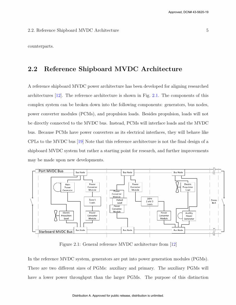
2.2 Reference Shipboard MVDC Architecture
A reference shipboard MVDC power architecture has been developed for aligning researched
architectures [12]. The reference architecture is shown in Fig. 2.1. The components of this
complex system can be broken down into the following components: generators, bus nodes,
power converter modules (PCMs), and propulsion loads. Besides propulsion, loads will not
be directly connected to the MVDC bus. Instead, PCMs will interface loads and the MVDC
bus. Because PCMs have power converters as its electrical interfaces, they will behave like
CPLs to the MVDC bus [19] Note that this reference architecture is not the final design of a
shipboard MVDC system but rather a starting point for research, and further improvements
may be made upon new developments.
Figure 2.1: General reference MVDC architecture from [12]
In the reference MVDC system, generators are put into power generation modules (PGMs).
There are two different sizes of PGMs: auxiliary and primary. The auxiliary PGMs will
have a lower power throughput than the larger PGMs. The purpose of this distinction
Approved, DCN# 43-5620-19
Distribution A. Approved for public release, distribution is unlimited.

6 Chapter 2. Review of Literature
is to ensure the PGMs online are running at maximum fuel efficiency operating points.
Generators operate at large time constants, meaning they will be slow in responding to
fast perturbations on the MVDC bus. Also, generators cannot quickly ramp their power
throughput to singlehandedly power pulsed loads.
Electric propulsion is the largest constantly running power load type in a shipboard MVDC
system [22]. Propulsion power consumption can be adjusted at a slightly faster time constant
than generators. The adjustment of its power consumption will affect the ship’s actual
movement speed, but they can be used to provide some bus voltage stabilization services.
The propulsion power consumption can be temporarily shed to redirect power to a different
load while the generators catch up. Also, the propulsion can also temporarily absorb excess
generation whenever a load turns off. This is done by having the ship temporarily move faster
than its target speed while the generators slowly reduce power throughput. Unfortunately,
these propulsion systems still do not operate at fast enough time constants to fully buffer a
large pulsed load [12].
The PCMs are designed to be modular and scalable in terms of what downstream loads
it can support. The PCMs will have an internal DC bus and ES that is bi-directional to
its internal DC bus. A set of power converters will interface the internal DC bus with the
MVDC bus. Another set of power converters will feed power from the internal DC bus to
downstream loads. There are two proposed variants for the PCMs: PCM-1A and PCM-1B.
The PCM-1A is intended for loads up to the maximum of several single digit megawatts and
to support small pulsed loads up to 1MW [9]. A generalized PCM-1A layout is shown in
Fig. 2.2. The PCM-1B is intended for loads in the order of tens of MW and mainly intended
to support very large pulsed loads [9].
Approved, DCN# 43-5620-19
Distribution A. Approved for public release, distribution is unlimited.
2.2. Reference Shipboard MVDC Architecture 7
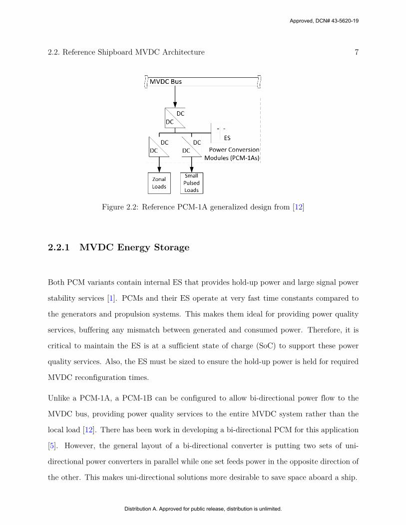
Figure 2.2: Reference PCM-1A generalized design from [12]
2.2.1 MVDC Energy Storage
Both PCM variants contain internal ES that provides hold-up power and large signal power
stability services [1]. PCMs and their ES operate at very fast time constants compared to
the generators and propulsion systems. This makes them ideal for providing power quality
services, buffering any mismatch between generated and consumed power. Therefore, it is
critical to maintain the ES is at a sufficient state of charge (SoC) to support these power
quality services. Also, the ES must be sized to ensure the hold-up power is held for required
MVDC reconfiguration times.
Unlike a PCM-1A, a PCM-1B can be configured to allow bi-directional power flow to the
MVDC bus, providing power quality services to the entire MVDC system rather than the
local load [12]. There has been work in developing a bi-directional PCM for this application
[5]. However, the general layout of a bi-directional converter is putting two sets of uni-
directional power converters in parallel while one set feeds power in the opposite direction of
the other. This makes uni-directional solutions more desirable to save space aboard a ship.
Approved, DCN# 43-5620-19
Distribution A. Approved for public release, distribution is unlimited.

8 Chapter 2. Review of Literature
2.2.2 Fault Clearing Hold-Up Power
The hold-up power functionality is required due to the fault clearing process for the MVDC
bus. DC power systems do not have a zero voltage crossing unlike AC systems. In an AC
system, to isolate a fault, a physical disconnect switch is sufficient as there are points where
the voltage is zero, breaking any electrical arcs. In a MVDC system, the MVDC bus must
be de-energized before switching can occur.
To clear a MVDC bus fault, switching is done to isolate the faulty bus segment. After
the fault is isolated, more switching is done on the MVDC bus to reconfigure its power
distribution routing. Therefore, all loads will lose power from the MVDC bus and must
rely on their local ES during this entire process [21]. Since some of these critical loads can
consume large amounts of power, the ES capacity can be fairly large. Also, the ES must
maintain a fairly high SoC to ensure that hold-up energy is always available for when a fault
occurs.
Depending on the MVDC bus fault protection topology used, protective devices such as
a solid state DC breaker must be added to all MVDC bus power sources [8], consuming
additional space and tonnage resources. Bi-directional PCM-1Bs or ES directly attached to
the MVDC bus are considered power sources. Therefore, there can be even more space and
tonnage savings for implementing PCM ES in a uni-directional configuration.
2.2.3 Large Signal Stabilization
Large signal stability generally refers to a how well a system can compensate or recover from
a very large perturbation that causes great deviations from designed operating points. CPLs
make the MVDC system non-linear, but for small signal stability, the stability criteria is
often linearized along set operating points [2]. However, such a criteria does not apply when
Approved, DCN# 43-5620-19
Distribution A. Approved for public release, distribution is unlimited.

2.2. Reference Shipboard MVDC Architecture 9
large disturbances bring the system outside those operating points. Large signal stability is
required to handle the non-linear behavior of the system.
An example of a large signal perturbation would be loads that have wide power consumption
swings, such as pulsed loads. Power pulsing can cause drastic voltage sagging, and the peak
pulsed load power consumption can quickly exceed on-line generation. The peak power
and ramp rate of large pulsed loads can easily out pace generators. The ES is critical in
compensating for the slow generators and limit drastic system operating point changes [22].
To prevent pulsed loads from transmitting its large destabilizing effect onto the MVDC bus,
the local PCM ES is used for large signal stabilization. The ES balances the large mismatch
between available generation and power consumption of the pulsed load [25]. The PCM
slowly ramps its power consumption from the MVDC bus in a stable manner while the ES
supplies or absorbs the missing or excess power of the pulse. This way, the generators will
only see a slow ramping load on the MVDC bus. The ES will slowly discharge of recharge
later on to normalize its SoC.
2.2.4 Small Signal Stabilization
Small signal stability describes whether a system maintains a stable state by its inherent
responses when disturbed by a small, continuous disturbance. Such disturbances within a
shipboard MVDC system can come from various sources such as:
• Generator output impedance and ripple voltage
• Bus resistance, inductance, and/or capacitance interactions
• Constant power loads responding to bus voltage fluctuations
• System controllers making slight adjustments
Approved, DCN# 43-5620-19
Distribution A. Approved for public release, distribution is unlimited.

10 Chapter 2. Review of Literature
In power systems, small signal stability is provided by damping the system responses to
converge towards a set value. This can be done by adding passive components such as
inductors and capacitors, or by tuning control variables. In a shipboard power system, it
is ideal that small signal stability requires the minimal amount of added hardware to save
space and weight. Also, if the MVDC system reconfigures its power distribution routing
due to a fault, the new configuration may change the MVDC bus’s electrical characteristics
and small signal stability. A tunable control variable is easier to adjust than changing the
stabilizing hardware.
2.3 Negative Load Virtual Stabilization
It is possible to emulate stabilizing circuit hardware by implementing the behavior in a
control loop. This is called a virtual stabilizer. An example would be a DC/DC converter
sourcing or draining current mimicking a capacitor model. From there, instead of changing
a real capacitor’s capacitance, the converter’s controller will only need to change a control
variable to change its effective capacitance. A virtual stabilizer can be implemented in the
PCMs of a MVDC system.
As mentioned before, having PCMs capable of bi-directional power flow to the MVDC bus
will require additional hardware, which is undesirable. A virtual stabilizer can function off
uni-directional PCMs by using a negative load configuration. In a negative load stabilizer, a
load’s consumed power is reduced or increased as if the stabilizer is in parallel with the load.
However, negative load stabilizers are limited by the power consumed by the real load and
can never operate without the real load consuming power. There are examples of negative
load virtual stabilizers in literature outside of shipboard MVDC applications.
[26] works with a 48V DC circuit with RLC parasitics in front of a uni-directional DC/DC
Approved, DCN# 43-5620-19
Distribution A. Approved for public release, distribution is unlimited.

2.3. Negative Load Virtual Stabilization 11
converter. [26] implemented various virtual negative load stabilizer configurations such as
parallel RC, parallel RL, series RL, and parallel RLC. The paper deemed that the impact
of the virtual stabilizer on the down stream CPL was negligible.
[17] added a virtual parallel capacitor as a stabilizer to satisfy P < RCV 2
Lto dampen the DC
bus RLC parasitics with a CPL motor, guaranteeing small signal stability. Despite the paper
not stating this, it should be noted that the control loop used in this paper actually uses a
virtual parallel RC stabilizer. The virtual R component was introduced in the control loop’s
low-pass filter. No where in this paper was the virtual resistor mentioned, but analysis was
done including the component. This paper assumed the motor controls were efficient enough
to not be affected by the stabilizer’s power fluctuations.
Though a shipboard MVDC system has higher power and voltage levels than these papers,
there are many advantages that a shipboard MVDC can have with negative load virtual
stabilizers. The system can be fine tuned by software after any MVDC bus reconfiguration,
and the PCM has internal ES that can cancel any power fluctuations on the load. With such
a stabilizer implemented in existing hardware, there can be space and weight savings, too.
Approved, DCN# 43-5620-19
Distribution A. Approved for public release, distribution is unlimited.
Chapter 3
Pulsed Power Loads
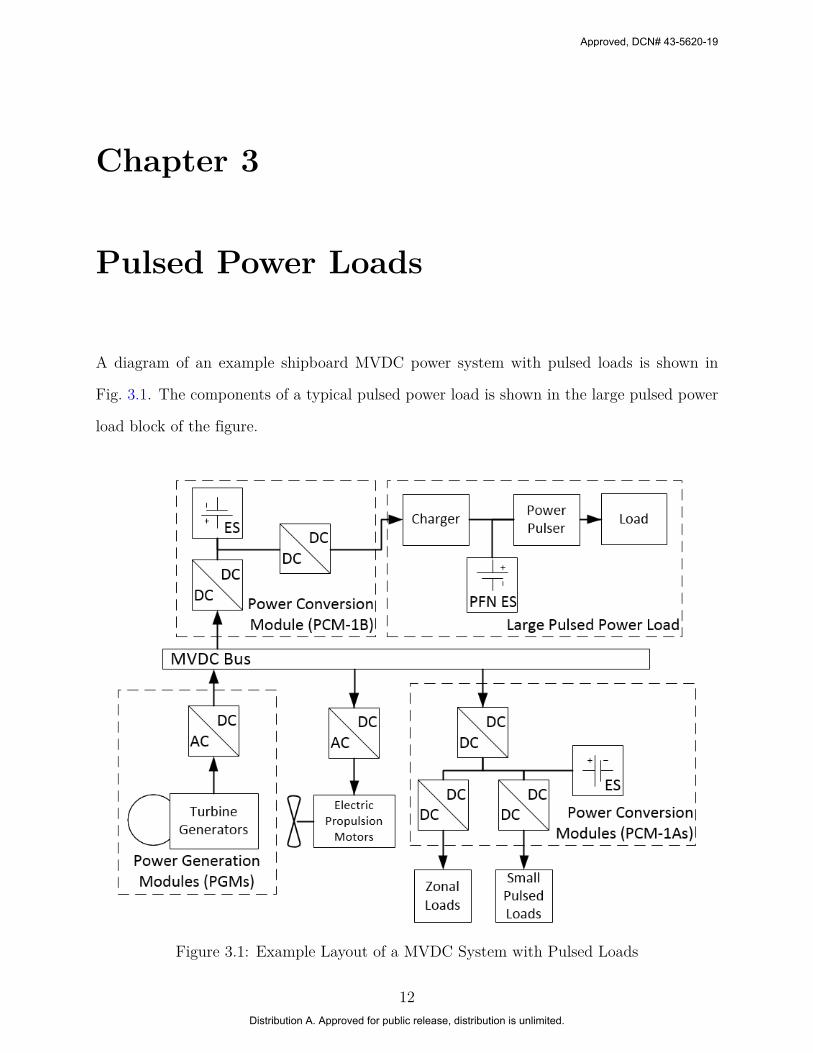
A diagram of an example shipboard MVDC power system with pulsed loads is shown in
Fig. 3.1. The components of a typical pulsed power load is shown in the large pulsed power
load block of the figure.
Figure 3.1: Example Layout of a MVDC System with Pulsed Loads
12
Approved, DCN# 43-5620-19
Distribution A. Approved for public release, distribution is unlimited.

13
A typical pulsed power load contains a pulse forming network (PFN) to supply the end load’s
power pulse. This is because a pulsed load often require a fast peak power than cannot be
supplied by traditional power systems. A PFN generally consists of: its own fast discharge
ES, a charger to charge the PFN ES, and an output power pulser that generates the desired
pulse shape. A PFN’s ES will slowly charge up before suddenly releasing it to drive the load.
In shipboard MVDC, the shipboard MVDC system will only see the charging of the pulsed
load’s PFN ES [23]. Therefore, the MVDC system will never see the actual power pulse
at the end load within the pulsed load. However, the charging power curve of a PFN can
be very aggressive, where the pulsed load charging itself is a power pulse. This is because
pulsed loads may need to operate multiple times a minute, requiring a train of power pulses
to recharge it [22]. Recharging the all of the ES must be done quickly enough to maintain
its desired rate of use.
With the entire MVDC system, the fast PCM ES will be used to buffer the large transient
power consumption of the pulsed load charging its PFNs. The faster PFN ES within the
pulsed load buffers the even larger and shorter power pulse for the end load. Basically, the
same energy from the generator is having its power delivery time shortened and peak power
increased at each successive ES device.
To better understand the functionality of a pulsed load, a controls system was implemented
and experimentally tested for a prototype pulsed load. The pulsed load prototype employs
capacitor-based PFN ES, and uses thyristor-based switching for pulse forming. A circuit of
the pulsed load is shown in Fig. 3.2
In this pulsed load prototype, the PFN ES is divided into separate capacitor banks, where
the controls system will selectively charge them using relays. The charger itself can be
controlled to charge the desired amount of energy. The gate drivers are triggered by the
Approved, DCN# 43-5620-19
Distribution A. Approved for public release, distribution is unlimited.
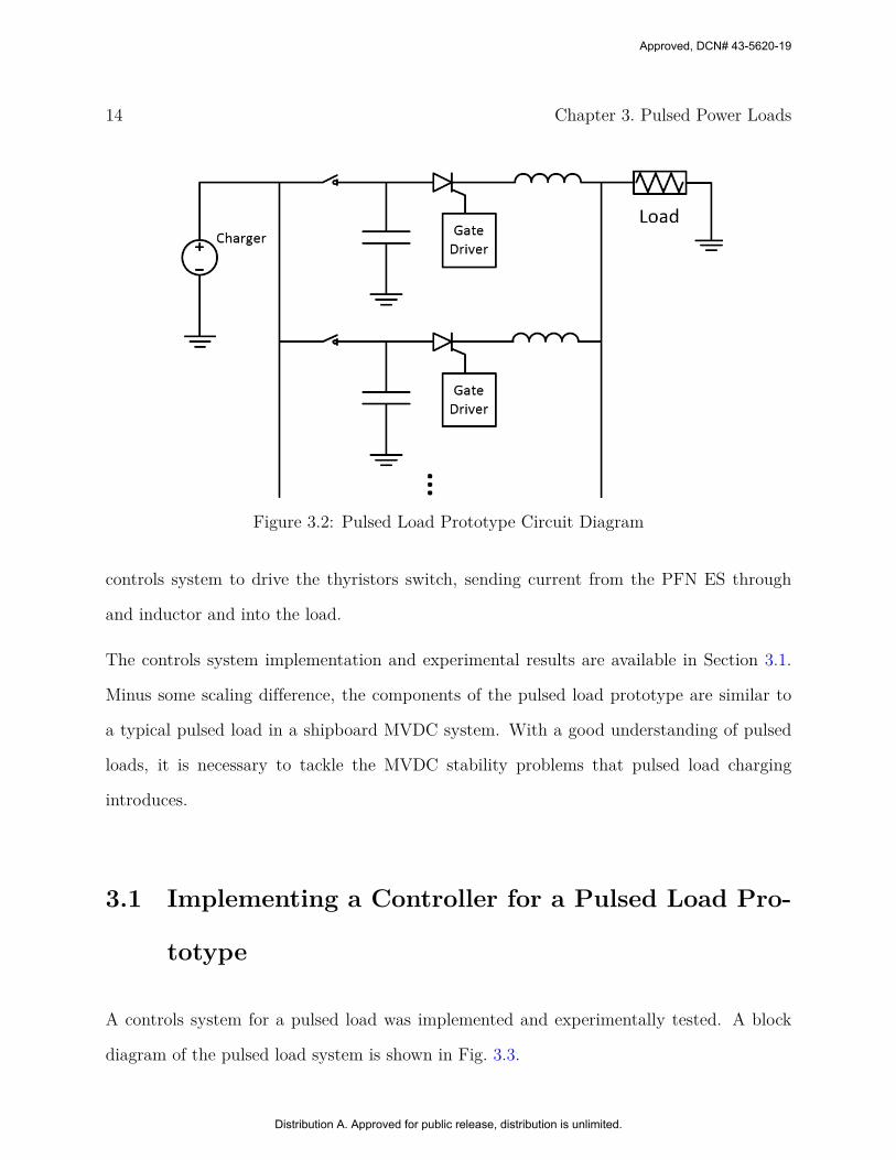
14 Chapter 3. Pulsed Power Loads
Figure 3.2: Pulsed Load Prototype Circuit Diagram
controls system to drive the thyristors switch, sending current from the PFN ES through
and inductor and into the load.
The controls system implementation and experimental results are available in Section 3.1.
Minus some scaling difference, the components of the pulsed load prototype are similar to
a typical pulsed load in a shipboard MVDC system. With a good understanding of pulsed
loads, it is necessary to tackle the MVDC stability problems that pulsed load charging
introduces.
3.1 Implementing a Controller for a Pulsed Load Pro-
totype
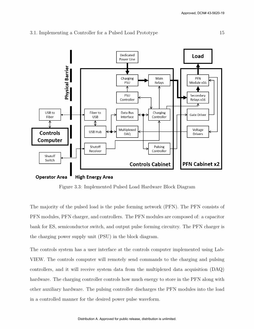
A controls system for a pulsed load was implemented and experimentally tested. A block
diagram of the pulsed load system is shown in Fig. 3.3.
Approved, DCN# 43-5620-19
Distribution A. Approved for public release, distribution is unlimited.
3.1. Implementing a Controller for a Pulsed Load Prototype 15
Figure 3.3: Implemented Pulsed Load Hardware Block Diagram
The majority of the pulsed load is the pulse forming network (PFN). The PFN consists of
PFN modules, PFN charger, and controllers. The PFN modules are composed of: a capacitor
bank for ES, semiconductor switch, and output pulse forming circuitry. The PFN charger is
the charging power supply unit (PSU) in the block diagram.
The controls system has a user interface at the controls computer implemented using Lab-
VIEW. The controls computer will remotely send commands to the charging and pulsing
controllers, and it will receive system data from the multiplexed data acquisition (DAQ)
hardware. The charging controller controls how much energy to store in the PFN along with
other auxiliary hardware. The pulsing controller discharges the PFN modules into the load
in a controlled manner for the desired power pulse waveform.
Approved, DCN# 43-5620-19
Distribution A. Approved for public release, distribution is unlimited.

16 Chapter 3. Pulsed Power Loads
If this system were to be installed in a shipboard MVDC system, the entire PFN and load
would be considered the pulsed load. The PFN charging power would be the power pulse
seen by the MVDC system. In Fig. 3.3, the dedicated power line would represent the MVDC
PCM power source to its downstream loads.
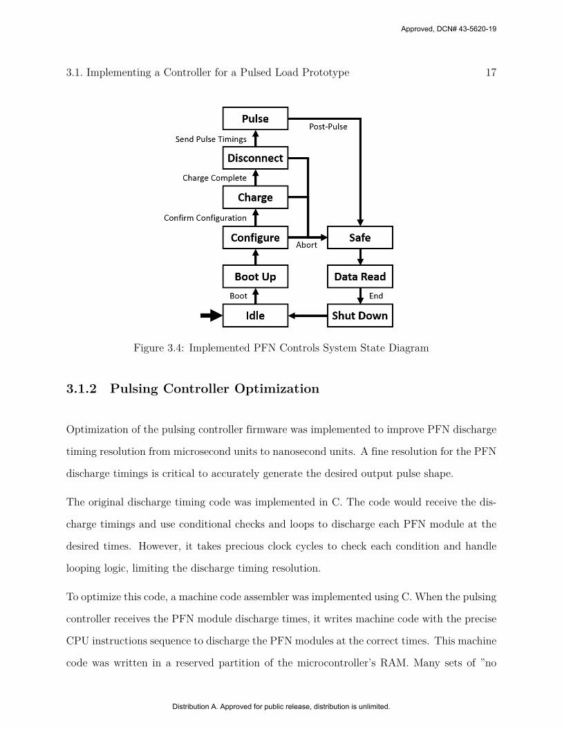
3.1.1 Pulsed Load Control Overview
The implemented controls system is operated by a state machine implemented in LabVIEW.
The states are shown below in Fig. 3.4. The states basically correspond to the steps needed
to operate a typical pulsed load.
First, the system operator boots up the controls system from an idle state. The operator
configures the PFN along with running any auxiliary setup required by the pulsed load.
The control system then charges the PFN modules to the specifications of its configuration,
and disconnects the PFN charging power supply after charging is complete. From there,
the pulse timings are sent to the PFN, and the PFN outputs the power pulse to the pulsed
load. After pulsing is completed, the PFN safes itself from any residual energy. The software
gathers any collected data from various sensors in the system and stores it for later analysis.
Afterwards, the controls system shuts down the PFN, awaiting the operator to boot it up
for another pulse.
The implemented controls system software is sophisticated in that it automates many pro-
cesses such as charging, preventing operator error. Error detection and automatic pulse
aborting is implemented to protect the hardware from damage when an anomaly is de-
tected. Due to the high energy nature of pulsed loads, the system was design to fail into a
safe state with whatever surviving hardware remains after a fault.
Approved, DCN# 43-5620-19
Distribution A. Approved for public release, distribution is unlimited.
3.1. Implementing a Controller for a Pulsed Load Prototype 17
Figure 3.4: Implemented PFN Controls System State Diagram
3.1.2 Pulsing Controller Optimization
Optimization of the pulsing controller firmware was implemented to improve PFN discharge
timing resolution from microsecond units to nanosecond units. A fine resolution for the PFN
discharge timings is critical to accurately generate the desired output pulse shape.
The original discharge timing code was implemented in C. The code would receive the dis-
charge timings and use conditional checks and loops to discharge each PFN module at the
desired times. However, it takes precious clock cycles to check each condition and handle
looping logic, limiting the discharge timing resolution.
To optimize this code, a machine code assembler was implemented using C. When the pulsing
controller receives the PFN module discharge times, it writes machine code with the precise
CPU instructions sequence to discharge the PFN modules at the correct times. This machine
code was written in a reserved partition of the microcontroller’s RAM. Many sets of ”no
Approved, DCN# 43-5620-19
Distribution A. Approved for public release, distribution is unlimited.
18 Chapter 3. Pulsed Power Loads
operation,” or NOP, CPU instructions were used to idle the microcontroller until the CPU
program counter reaches instructions to send a PFN module discharge signal. Therefore,
all of the condition checking and loop logic were replaced by the precise wait time needed
by the discharge timings. For long wait times between discharge signals, a loop of NOPs is
generated, and filler NOPs are added to the exact needed wait time. The general logic of
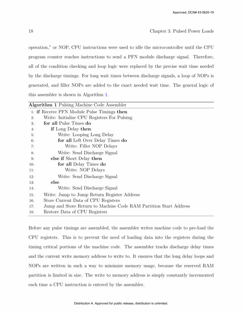
this assembler is shown in Algorithm 1.
Algorithm 1 Pulsing Machine Code Assembler1: if Receive PFN Module Pulse Timings then2: Write: Initialize CPU Registers For Pulsing3: for all Pulse Times do4: if Long Delay then5: Write: Looping Long Delay6: for all Left Over Delay Times do7: Write: Filler NOP Delays8: Write: Send Discharge Signal9: else if Short Delay then
10: for all Delay Times do11: Write: NOP Delays12: Write: Send Discharge Signal13: else14: Write: Send Discharge Signal15: Write: Jump to Jump Return Register Address16: Store Current Data of CPU Registers17: Jump and Store Return to Machine Code RAM Partition Start Address18: Restore Data of CPU Registers
Before any pulse timings are assembled, the assembler writes machine code to pre-load the
CPU registers. This is to prevent the need of loading data into the registers during the
timing critical portions of the machine code. The assembler tracks discharge delay times
and the current write memory address to write to. It ensures that the long delay loops and
NOPs are written in such a way to minimize memory usage, because the reserved RAM
partition is limited in size. The write to memory address is simply constantly incremented
each time a CPU instruction is entered by the assembler.
Approved, DCN# 43-5620-19
Distribution A. Approved for public release, distribution is unlimited.

3.1. Implementing a Controller for a Pulsed Load Prototype 19
Once the discharge timings are assembled, the current data in the CPU registers are stored,
because the C code compiler does not expect and handle the injected machine code modifying
CPU register values. The C code jumps to the assembled machine code, pre-loads the
registers, and runs the discharge timing code. Afterwards, the machine code returns to
where the C code left off, and the C code restores the CPU registers before continuing on as
normal as if nothing happened.
This optimization is hardware specific to PIC32 microcontrollers, which was used in this
implementation. A weakness of an assembler optimization solution is that it is not portable to
other microarchitectures. Ideally, for parallel timing operations, a FPGA would be used here.
However, the pulsing controller has a lot of other logic that would require a microcontroller
to easily implement, and the optimized implementation produces more than adequate results
for this system.
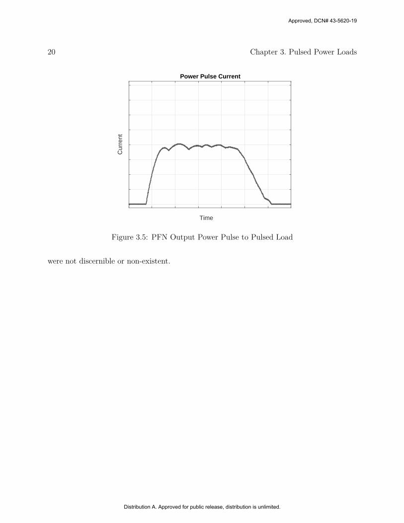
3.1.3 Pulsed Power Load Experimental Results
The implemented controls system was used to experimentally test the complete pulsed load
system. Various experiments were done with successful results, confirming the functionality
of the controls system. An example output power pulse from the PFN is shown in Fig. 3.5.
The ideal output of the PFN is a square pulse at a set amount of peak power for a set amount
of time, so the goal is to have the implemented PFN achieve a square pulse as closely as
possible. However, with real hardware, there are rise and fall times for the PFN. Also, the
peak current of the square pulse is not flat due to the output current waveforms of a single
PFN module. Instead, controlled PFN module discharging at the correct times are used to
generate an as flat as possible peak current, which is made possible by the optimized pulsing
controller. Thanks to the optimized resolution of the pulsing controller, pulse timing errors
Approved, DCN# 43-5620-19
Distribution A. Approved for public release, distribution is unlimited.
20 Chapter 3. Pulsed Power Loads
Time
Cur
rent
Power Pulse Current
Figure 3.5: PFN Output Power Pulse to Pulsed Load
were not discernible or non-existent.
Approved, DCN# 43-5620-19
Distribution A. Approved for public release, distribution is unlimited.
Chapter 4
Proposed MVDC Small Signal
Stabilizer
This thesis designs a negative load virtual small signal stabilizer in a uni-directional PCM
for a shipboard MVDC system to support pulsed loads. The ES will be used to cancel out
the stabilizer’s power fluctuations on the downstream load. This stabilizer should guarantee
small signal stability across a wide power range seen in pulsed loads. Because pulsed loads
will greatly change its equivalent load resistance on the MVDC bus, this thesis proposes to
dynamically tune the virtual stabilizer with the load power consumption.
To implement the stabilizer, a working MVDC model needs to be developed. Also, control
loops must be made for the various functions of the PCM. From there, a small signal stability
criteria needs to be developed. Finally, method of tuning the stabilizer to be stable is needed.
4.1 Simplified MVDC Model
As mentioned before, the reference MVDC model is fairly complex. For the sake of devel-
oping and testing a this negative load stabilizer design, the MVDC system model has been
simplified into what is shown in Fig. 4.1. This model has a single ideal generator with volt-
age droop. There is a generic reference design PCM which has an internal DC bus with a
bus capacitor, internal ES, and the downstream constant power load. Each of the DC/DC
21
Approved, DCN# 43-5620-19
Distribution A. Approved for public release, distribution is unlimited.

22 Chapter 4. Proposed MVDC Small Signal Stabilizer
power converters within the PCM have power and power ramp rate limitations and follow
the power flow of a reference PCM-1A.
Figure 4.1: Simplified MVDC model used for testing.
The is a RLC component that is a simplified representation of the electrical characteristics of
a generator, power converter with filter, and MVDC bus as discussed in Section 2.2.4. This
was done assuming that the system could be represented as such done in [12]. This model
can be converted to a more complex model by: separating out the electrical characteristics,
expanding the power converter with input filter values and switching, and/or add a parallel
PCM on the MVDC bus.
Without the virtual stabilizer in the simplified circuit, the small signal stability criteria is
P <RCV 2
MVDC
L, (4.1)
where P is the power consumption of the PCM from the MVDC bus, VMVDC is the MVDC
bus voltage at the PCM, and R, L, and C are the RLC characteristics of the MVDC bus.
Note that VMVDC may fluctuate due to noise or voltage droop, and P will also change
drastically during power pulsing. Therefore, the above small signal stability criteria must
Approved, DCN# 43-5620-19
Distribution A. Approved for public release, distribution is unlimited.

4.2. Control Loops 23
considered for all operating points.
4.2 Control Loops
A set of control loops were developed to control the PCM’s internal behavior and interactions
with the MVDC bus. The controller maintains the internal bus voltage while allowing the
virtual stabilizer to inject power on its MVDC input power converter. Also, the controller
manages and utilizes the ES while ensuring power quality to the downstream constant power
load. The ES control loop uses the ES for internal bus regulation while the MVDC side power
converter control loop attempts to balance power consumption with power sourced from the
MVDC bus.
A number of the following control loops used in this thesis were adapted from other papers.
Besides the virtual stabilizer control loop, the PCM control loops were adapted from [6].
These control loops were intended for a zonal DC bus with a generator, ES, PCM power
input from an MVDC bus, and CPL. These control loops were not tested with pulsed power
loads.
The MVDC bus to PCM internal DC bus DC/DC power converter control loop adapted from
[6] is shown in Fig. 4.2. The control loop’s iG0 has been removed as there is no generator
inside the reference PCM design. Also, the controls delay transfer functions have been
removed to simplify the model.
Figure 4.2: MVDC Side Power Converter Control Loop from [6]
Approved, DCN# 43-5620-19
Distribution A. Approved for public release, distribution is unlimited.
24 Chapter 4. Proposed MVDC Small Signal Stabilizer
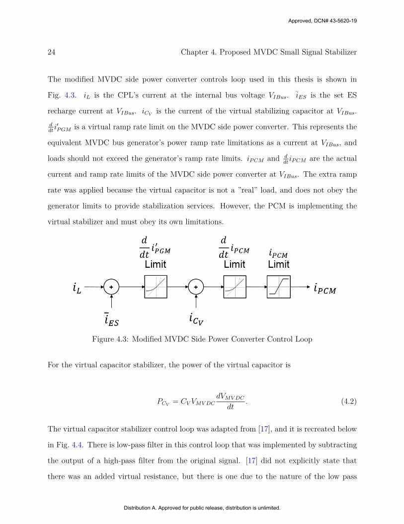
The modified MVDC side power converter controls loop used in this thesis is shown in
Fig. 4.3. iL is the CPL’s current at the internal bus voltage VIBus. iES is the set ES
recharge current at VIBus. iCVis the current of the virtual stabilizing capacitor at VIBus.
ddti′PGM is a virtual ramp rate limit on the MVDC side power converter. This represents the
equivalent MVDC bus generator’s power ramp rate limitations as a current at VIBus, and
loads should not exceed the generator’s ramp rate limits. iPCM and ddtiPCM are the actual
current and ramp rate limits of the MVDC side power converter at VIBus. The extra ramp
rate was applied because the virtual capacitor is not a ”real” load, and does not obey the
generator limits to provide stabilization services. However, the PCM is implementing the
virtual stabilizer and must obey its own limitations.
Figure 4.3: Modified MVDC Side Power Converter Control Loop
For the virtual capacitor stabilizer, the power of the virtual capacitor is
PCV= CV VMVDC
dVMVDC
dt. (4.2)
The virtual capacitor stabilizer control loop was adapted from [17], and it is recreated below
in Fig. 4.4. There is low-pass filter in this control loop that was implemented by subtracting
the output of a high-pass filter from the original signal. [17] did not explicitly state that
there was an added virtual resistance, but there is one due to the nature of the low pass
Approved, DCN# 43-5620-19
Distribution A. Approved for public release, distribution is unlimited.

4.2. Control Loops 25
filter in the control loop.
Figure 4.4: Original Virtual Capacitor Stabilizer from [17]
This thesis converted the control loop’s virtual capacitor’s power PV C to the virtual capac-
itor’s, or stabilizer’s, current iV C at VIBus. Hardware limits were also incorporated on the
virtual capacitor. These limits were applied because the converter hardware cannot com-
pletely replicate a real RC stabilizer behavior, and the control loop should reflect this. Also,
the low-pass filter configuration was simplified in this thesis’s control loop into a transfer
function based on the virtual resistor RV and capacitor CV values.
Figure 4.5: Modified MVDC Side Power Converter Control Loop
PCM hardware limits were applied to the virutal capacitor, because the PCM is emulating
the ”real” equivalent hardware. As stated before, the ramp rate limit ddti′PGM is a virtual
limit to follow an MVDC bus generator’s ramp rate limits. The virtual stabilizer is not
Approved, DCN# 43-5620-19
Distribution A. Approved for public release, distribution is unlimited.
26 Chapter 4. Proposed MVDC Small Signal Stabilizer
a ”real” load, and it must function as closely to a real stabilizer to provide stabilization.
Therefore, the generator’s ramp rates were ignored and the PCM’s ramp rate limits were
used instead. Furthermore, the PCM’s power limits were applied in plus-minus form as the
stabilizer can only change PCM power to zero at full PCM power or to full power at no PCM
power. Later on in the PCM’s control block, the iCVterm will be added up and have the
PCM’s ramp rate and power limitations re-applied to ensure all of the PCM’s limitations
are obeyed.
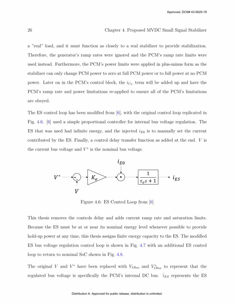
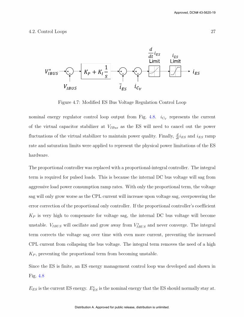
The ES control loop has been modified from [6], with the original control loop replicated in
Fig. 4.6. [6] used a simple proportional controller for internal bus voltage regulation. The
ES that was used had infinite energy, and the injected iE0 is to manually set the current
contributed by the ES. Finally, a control delay transfer function as added at the end. V is
the current bus voltage and V ∗ is the nominal bus voltage.
Figure 4.6: ES Control Loop from [6]
This thesis removes the controls delay and adds current ramp rate and saturation limits.
Because the ES must be at or near its nominal energy level whenever possible to provide
hold-up power at any time, this thesis assigns finite energy capacity to the ES. The modified
ES bus voltage regulation control loop is shown in Fig. 4.7 with an additional ES control
loop to return to nominal SoC shown in Fig. 4.8.
The original V and V ∗ have been replaced with VIBus and V ∗IBus to represent that the
regulated bus voltage is specifically the PCM’s internal DC bus. iES represents the ES
Approved, DCN# 43-5620-19
Distribution A. Approved for public release, distribution is unlimited.
4.2. Control Loops 27
Figure 4.7: Modified ES Bus Voltage Regulation Control Loop
nominal energy regulator control loop output from Fig. 4.8. iCVrepresents the current
of the virtual capacitor stabilizer at VIBus as the ES will need to cancel out the power
fluctuations of the virtual stabilizer to maintain power quality. Finally, ddtiES and iES ramp
rate and saturation limits were applied to represent the physical power limitations of the ES
hardware.
The proportional controller was replaced with a proportional-integral controller. The integral
term is required for pulsed loads. This is because the internal DC bus voltage will sag from
aggressive load power consumption ramp rates. With only the proportional term, the voltage
sag will only grow worse as the CPL current will increase upon voltage sag, overpowering the
error correction of the proportional only controller. If the proportional controller’s coefficient
KP is very high to compensate for voltage sag, the internal DC bus voltage will become
unstable. VIBUS will oscillate and grow away from V ∗IBUS and never converge. The integral
term corrects the voltage sag over time with even more current, preventing the increased
CPL current from collapsing the bus voltage. The integral term removes the need of a high
KP , preventing the proportional term from becoming unstable.
Since the ES is finite, an ES energy management control loop was developed and shown in
Fig. 4.8
EES is the current ES energy. E∗ES is the nominal energy that the ES should normally stay at.
Approved, DCN# 43-5620-19
Distribution A. Approved for public release, distribution is unlimited.

28 Chapter 4. Proposed MVDC Small Signal Stabilizer
Figure 4.8: ES Energy Regulator Control Loop
The ES should not destabilize the DC buses and obey the generator limits when recharging or
discharging to nominal E∗ES, so the ES energy regulation is limited by the MVDC generator’s
ramp rate limits and PCM’s current limits. The ES will also never attempt to return to
nominal energy levels when the internal bus voltage VIBus is not within its tolerances Tol as
the ES’s first role is to regulate the internal DC bus voltage. A proportional controller was
used to return the ES to its nominal SoC, allowing a more aggressive charge/discharge the
further EES is from E∗ES.
The proportional controller’s coefficient KR must be large enough so that the ES will return
to nominal SoC fast enough, but it cannot be too large where the SoC EES will not stably
converge towards E∗ES. The KR term must follow the criteria KR < 1
VIBUS. This is because
E∗ES and EES are in units of Joules of energy, and the output of this control loop ¯iES is in
units of current at VIBUS. With KR = 1, VIBUS of power will be used to charge/discharge
1J of energy difference between EES and E∗ES. If VIBUS > 1, EES would overshoot and
never converge to E∗ES as >1W is used to charge/discharge the 1J error. Since VIBUS may
fluctuate, a safety margin on KR is required.
Approved, DCN# 43-5620-19
Distribution A. Approved for public release, distribution is unlimited.
4.2. Control Loops 29
4.2.1 Voltage Droop
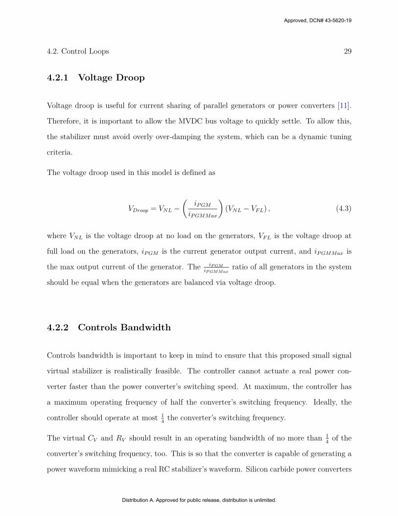
Voltage droop is useful for current sharing of parallel generators or power converters [11].
Therefore, it is important to allow the MVDC bus voltage to quickly settle. To allow this,
the stabilizer must avoid overly over-damping the system, which can be a dynamic tuning
criteria.
The voltage droop used in this model is defined as
VDroop = VNL −(
iPGM
iPGMMax
)(VNL − VFL) , (4.3)
where VNL is the voltage droop at no load on the generators, VFL is the voltage droop at
full load on the generators, iPGM is the current generator output current, and iPGMMax is
the max output current of the generator. The iPGM
iPGMMaxratio of all generators in the system
should be equal when the generators are balanced via voltage droop.
4.2.2 Controls Bandwidth
Controls bandwidth is important to keep in mind to ensure that this proposed small signal
virtual stabilizer is realistically feasible. The controller cannot actuate a real power con-
verter faster than the power converter’s switching speed. At maximum, the controller has
a maximum operating frequency of half the converter’s switching frequency. Ideally, the
controller should operate at most 14
the converter’s switching frequency.
The virtual CV and RV should result in an operating bandwidth of no more than 14
of the
converter’s switching frequency, too. This is so that the converter is capable of generating a
power waveform mimicking a real RC stabilizer’s waveform. Silicon carbide power converters
Approved, DCN# 43-5620-19
Distribution A. Approved for public release, distribution is unlimited.
30 Chapter 4. Proposed MVDC Small Signal Stabilizer
for MVDC applications are being developed, and they have higher switching frequencies than
their traditional silicon-only power electronics [4]. With silicon carbide power converters, the
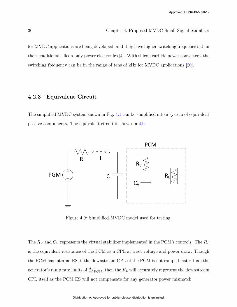
switching frequency can be in the range of tens of kHz for MVDC applications [20].
4.2.3 Equivalent Circuit
The simplified MVDC system shown in Fig. 4.1 can be simplified into a system of equivalent
passive components. The equivalent circuit is shown in 4.9.
Figure 4.9: Simplified MVDC model used for testing.
The RV and CV represents the virtual stabilizer implemented in the PCM’s controls. The RL
is the equivalent resistance of the PCM as a CPL at a set voltage and power draw. Though
the PCM has internal ES, if the downstream CPL of the PCM is not ramped faster than the
generator’s ramp rate limits of ddti′PGM , then the RL will accurately represent the downstream
CPL itself as the PCM ES will not compensate for any generator power mismatch.
Approved, DCN# 43-5620-19
Distribution A. Approved for public release, distribution is unlimited.

4.2. Control Loops 31
4.2.4 Transfer Function
Using the equivalent circuit representation of the MVDC system, a 3rd order transfer function
can be derived. CPLs act and can be modeled as a negative resistor [14]. Therefore, for
accurate modeling, RL is negative when calculating the transfer function. The transfer
function of the equivalent circuit is
VL
VDroop=
b1s+ b0a3s3 + a2s2 + a1s+ a0
, (4.4)
where
b1 = CVRVRL
b0 = RL
a3 = CCVLRLRV
a2 = CLRL + CVLRL − CVLRV + CCVRRLRV
a1 = CRRL − L+ CVRRL − CVRRV + CVRLRV
a0 = RL −R.
(4.5)
It is difficult to solve this transfer function analytically. To solve for CV and RV to maintain
a desired MVDC damping factor ζ, low-Q approximation was used.
Approved, DCN# 43-5620-19
Distribution A. Approved for public release, distribution is unlimited.

32 Chapter 4. Proposed MVDC Small Signal Stabilizer
4.3 Low-Q Approximation
Low-Q approximation allows order reduction of polynomials into their approximate 1st and
2nd order roots. In the equivalent circuit’s use case, the polynomial is the transfer func-
tion’s poles (denominator). This makes it possible to reasonably approximate the roots of
high order transfer functions. However, the roots must be real and well separated for low-Q
approximation to be accurate [18]. The further the roots are separated results in a more ac-
curate approximation. [18] shows the original mathematical proof for 2nd order polynomials,
and [13] has expanded low-Q approximation to a more general case to support higher than
2nd order polynomials.
[13] has also defined special cases where only two roots are close together. The close together
roots can remain in quadratic form while the other roots are in 1st order form. Only quadratic
roots were covered by [13], but it is theoretically possible to keep roots in higher order (e.g.
cubic) forms if more than 2 roots are close together. This section will only provide the low-
Q approximation methodology and formulation for the transfer function Eq. (4.4) for the
model in Fig. 4.9, but more information can be found about the general low-Q approximation
methodology in [13].
First, the inequalities used in low-Q approximation are defined using significant inequalities
(≫ and ≪). Let the term α represent how significant the inequality is. Therefore, if a≫ b,
then aα > b. This value is important for low-Q approximation as a smaller α means that
the roots are further separated and results in a more accurate approximation [18]. With a
more accurate approximation, the correctness of the stabilizer is greater, so it is important
to record how accurate the low-Q approximation was done.
Next, the transfer function D(s) must be converted into the standard low-Q approximation
form of
Approved, DCN# 43-5620-19
Distribution A. Approved for public release, distribution is unlimited.

4.3. Low-Q Approximation 33
D(s) = 1 + a1s+ a2s2 + a3s
3. (4.6)
To put the original transfer function Eq. (4.5) into standard form Eq. (4.6), simply divide
a1, a2, a3 by a0 in Eq. (4.5). This results in the standard form roots of:
a3 =a3a0
a2 =a2a0
a1 =a1a0
a0 =a0a0
= 1.
(4.7)
From Eq. (4.7), the D(s) in standard form is now:
D(s) = 1 + a1s+ a2s2 + a3s
3. (4.8)
In low-Q approximation, if all the roots are real and well separated, the roots can be separated
into only 1st order roots. Since Eq. (4.4) is a 3rd order transfer function and if all the
conditions are satisfied, there will only be three 1st order roots. Being 3rd order, there are
also two special cases for the low-Q approximation of Eq. (4.4). These special cases result
in one 1st order root and one 2nd order (quadratic) root.
The 2nd order roots from low-Q approximation are in the form of
1 +s
Qω0
+
(s
ω0
)2
. (4.9)
Approved, DCN# 43-5620-19
Distribution A. Approved for public release, distribution is unlimited.

34 Chapter 4. Proposed MVDC Small Signal Stabilizer
Using Eq. (4.9), the natural frequency ω0 can be extracted from the s2 coefficient. Then,
the Q factor Q can be solved for from the s coefficient. With the Q factor, the approximate
damping factor ζ of the circuit can be solved with
ζ =1
2Q. (4.10)
Finally, low-Q approximation for the circuit in Fig. 4.9 can be done in the following steps.
First, the normal low-Q approximation case’s conditions are checked.
For the normal case, if
|a1| ≫∣∣∣∣ a2a1
∣∣∣∣≫ ∣∣∣∣ a3a2∣∣∣∣ , (4.11)
then the roots of the denominator are
D(s) ≈ (1 + a1s)
(1 +
a2a1
s
)(1 +
a3a2
s
). (4.12)
Due to the 1st order roots, no natural frequency of the circuit can be low-Q approximated,
resulting in no resonating circuit to dampen. The roots in Eq. (4.12) are shown in an order
such that each successive root has a smaller time constant magnitude, which may be desirable
to know for characterizing the circuit behavior. However, the normal case is only possible
with certain values. Because it is desirable to shrink the real capacitor capacitance C as
much as possible, C will approach L. This will result in the normal case being violated and
often involve invoking the special low-Q approximation cases.
Approved, DCN# 43-5620-19
Distribution A. Approved for public release, distribution is unlimited.

4.3. Low-Q Approximation 35
4.3.1 Low-Q 1st Special Case
If the normal case condition Eq. (4.11) is violated by
|a1| ≫∣∣∣∣ a2a1
∣∣∣∣≫ ∣∣∣∣ a3a2∣∣∣∣ , (4.13)
but satisfies the inequality
∣∣∣∣ a22a3∣∣∣∣≫ |a1| ≫ ∣∣∣∣ a3a2
∣∣∣∣ , (4.14)
then the 1st special case roots are
D(s) ≈(1 + a1s+ a2s
2)(
1 +a3a2
s
). (4.15)
The 1st special case 2nd order root has an approximate natural frequency of
ω01 =
√1
a2, (4.16)
an approximate Q factor of
Q1 =1a1
ω01
, (4.17)
and an approximate damping factor of
ζ1 =1
2Q1
. (4.18)
Approved, DCN# 43-5620-19
Distribution A. Approved for public release, distribution is unlimited.

36 Chapter 4. Proposed MVDC Small Signal Stabilizer
Note that there are subscripts indicating that these approximate values were generated from
the 1st special case. This distinction is important, because when picking the stabilizer’s CV
and RV values, there are two possible value sets as the stabilizer’s values chose will affect
which special case that the circuit will fall under.
4.3.2 Low-Q 2nd Special Case
If the violation of condition Eq. (4.11) is
|a1| ≫∣∣∣∣ a2a1
∣∣∣∣ ≫ ∣∣∣∣ a3a2∣∣∣∣ , (4.19)
and satisfies
|a1| ≫∣∣∣∣ a2a1
∣∣∣∣≫ ∣∣∣∣ a0a3a21
∣∣∣∣ , (4.20)
then the 2nd special case roots are
D(s) ≈ (1 + a1s)
(1 +
a2a1
s2 +a3a1
s2). (4.21)
The 2nd special case 2nd order root has an approximate natural frequency of
ω02 =
√√√√ 1(a3a1
) , (4.22)
an approximate Q factor of
Approved, DCN# 43-5620-19
Distribution A. Approved for public release, distribution is unlimited.

4.3. Low-Q Approximation 37
Q2 =
1(a2a1
)ω02
, (4.23)
and an approximate damping factor of
ζ2 =1
2Q2
. (4.24)
It may be desirable to use virtual stabilizer values that cause the system to fall into a 2nd
special case low-Q approximation solution. This is due to how the successive roots in low-Q
approximation have a smaller time constant magnitude [13]. Using the 2nd case results in
the smaller time constant term becoming more dominant in the system’s response, causing
a faster response. Since the purpose of this stabilizer is to provide small signal stability,
a faster response by the system is desirable, and the earlier and slower root terms can be
compensated by a faster compensator. However, targeting for a solution in the 1st case can
also be desirable as the 1st case’s solution often has a smaller CV value.
4.3.3 Low-Q Solution Space
To visualize the low-Q approximation solution space, the following algorithm was used to
plot the damping factor in a space of CV and RV . The algorithm is a basic brute force
algorithm that numerically solves for each CV and RV value of the virtual stabilizer to find
the resulting system damping factor.
An example plot is shown in Fig. 4.10. There are two visible solution regions, and each
region corresponds to a special case. The special case solution regions generally sandwich
a forbidden region in between before merging at a high CV value. The forbidden region
is caused by the approximation falling outside of the normal and special cases, where the
Approved, DCN# 43-5620-19
Distribution A. Approved for public release, distribution is unlimited.

38 Chapter 4. Proposed MVDC Small Signal Stabilizer
Algorithm 2 Low-Q Approximation Brute-Force Damping Factor of Virtual RC Stabilizer1: Initialize R,L,C,RL
2: CV Set← Set of CV searched3: RV Set← Set of RV searched4: ζ ← Zero matrix of dimension [CV Set, RV Set]5: α← Desired Low-Q Approximation Accuracy6: for all CV in CV Set do7: for all RV in RV Set do8: a3, a2, a1, a0 ← Calculate Transfer Function(R,L,C,RL, CV , RV )9: a3, a2, a1 ← Normalize(a3, a2, a1, a0)
10: Calculate Case(a3, a2, a1)11: if Normal Case then12: ζ[CV , RV ]← No Damping Factor13: else if 1st Special Case then14: ζ[CV , RV ]← 1st Special Case Damping Factor15: else if 2nd Special Case then16: ζ[CV , RV ]← 2nd Special Case Damping Factor17: else18: ζ[CV , RV ]← Invalid19: Plot ζ
roots are not well separated. Roots that are not well separated results in less accurate low-Q
approximations. As the root separation tolerance α tightens, the forbidden region will grow
outward as closer roots will not be allowed.
It is visible that the solution in the 1st special case has a lower possible CV value for main-
taining critical damping. A smaller CV value is generally desirable, because it minimizes the
power required by the virtual capacitor to mimic a real capacitor. This is because the power
of the virtual capacitor, PCV, is linearly related to CV as shown in Eq. (4.2). Minimizing the
power required also minimizes the required energy utilized by the virtual capacitor during
damping actuation. This minimizes the range of the PCM power negatively affecting the
virtual stabilizer performance and minimizes ES energy usage. However, a higher RV from
the 2nd special case solution region can attenuate the dVMV DC
dtterm, using the low-pass filter,
which can offset the effects of a higher CV value. However, this entire discussion focuses
Approved, DCN# 43-5620-19
Distribution A. Approved for public release, distribution is unlimited.
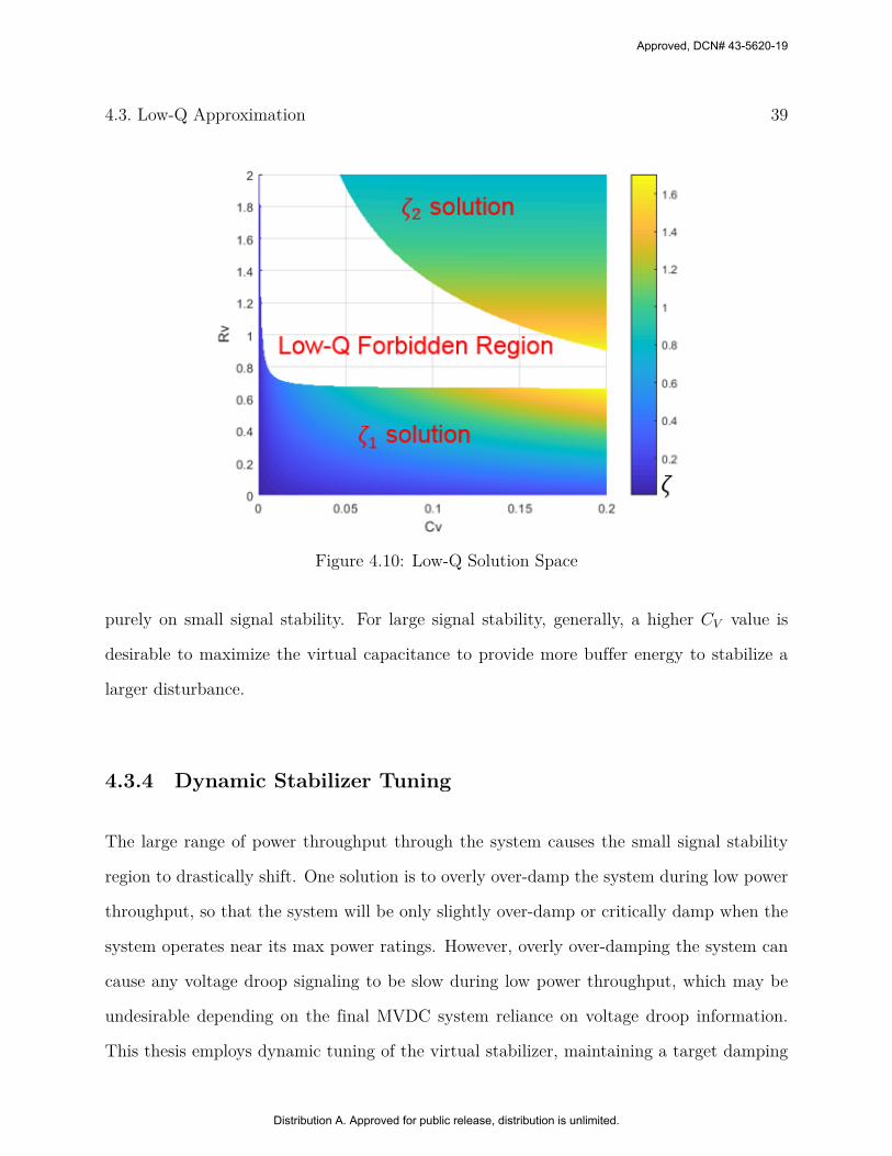
4.3. Low-Q Approximation 39
Figure 4.10: Low-Q Solution Space
purely on small signal stability. For large signal stability, generally, a higher CV value is
desirable to maximize the virtual capacitance to provide more buffer energy to stabilize a
larger disturbance.
4.3.4 Dynamic Stabilizer Tuning
The large range of power throughput through the system causes the small signal stability
region to drastically shift. One solution is to overly over-damp the system during low power
throughput, so that the system will be only slightly over-damp or critically damp when the
system operates near its max power ratings. However, overly over-damping the system can
cause any voltage droop signaling to be slow during low power throughput, which may be
undesirable depending on the final MVDC system reliance on voltage droop information.
This thesis employs dynamic tuning of the virtual stabilizer, maintaining a target damping
Approved, DCN# 43-5620-19
Distribution A. Approved for public release, distribution is unlimited.
40 Chapter 4. Proposed MVDC Small Signal Stabilizer
factor near critical damping for the entire power operating range of the system. This al-
lows voltage levels to quickly converge to its voltage droop levels, minimizing voltage droop
information transmission time.
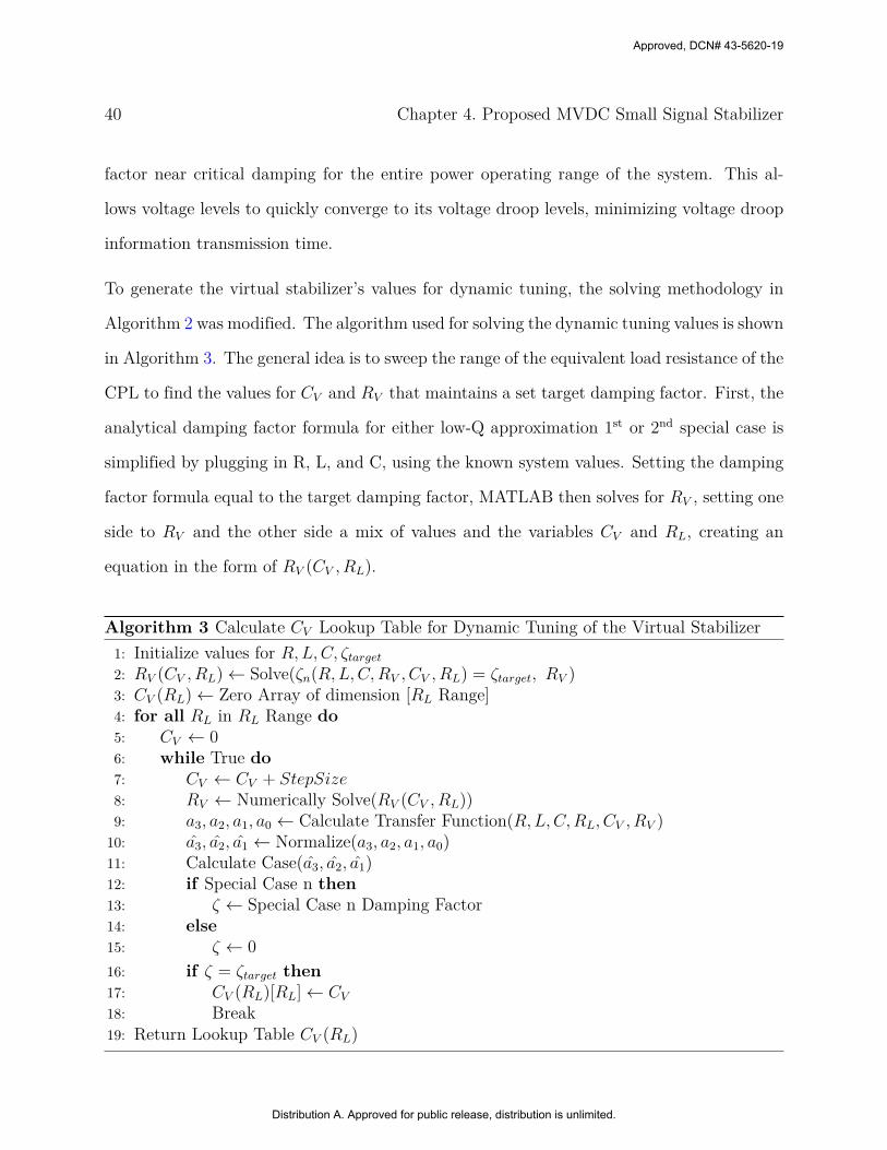
To generate the virtual stabilizer’s values for dynamic tuning, the solving methodology in
Algorithm 2 was modified. The algorithm used for solving the dynamic tuning values is shown
in Algorithm 3. The general idea is to sweep the range of the equivalent load resistance of the
CPL to find the values for CV and RV that maintains a set target damping factor. First, the
analytical damping factor formula for either low-Q approximation 1st or 2nd special case is
simplified by plugging in R, L, and C, using the known system values. Setting the damping
factor formula equal to the target damping factor, MATLAB then solves for RV , setting one
side to RV and the other side a mix of values and the variables CV and RL, creating an
equation in the form of RV (CV , RL).
Algorithm 3 Calculate CV Lookup Table for Dynamic Tuning of the Virtual Stabilizer1: Initialize values for R,L,C, ζtarget2: RV (CV , RL)← Solve(ζn(R,L,C,RV , CV , RL) = ζtarget, RV )3: CV (RL)← Zero Array of dimension [RL Range]4: for all RL in RL Range do5: CV ← 06: while True do7: CV ← CV + StepSize8: RV ← Numerically Solve(RV (CV , RL))9: a3, a2, a1, a0 ← Calculate Transfer Function(R,L,C,RL, CV , RV )
10: a3, a2, a1 ← Normalize(a3, a2, a1, a0)11: Calculate Case(a3, a2, a1)12: if Special Case n then13: ζ ← Special Case n Damping Factor14: else15: ζ ← 0
16: if ζ = ζtarget then17: CV (RL)[RL]← CV
18: Break19: Return Lookup Table CV (RL)
Approved, DCN# 43-5620-19
Distribution A. Approved for public release, distribution is unlimited.

4.3. Low-Q Approximation 41
A sweep searching for a CV value is done for each RL value, and the CV value must result
in the targeted damping factor. By plugging RV (CV , RL) into the transfer function and
running low-Q approximation, the RV term is therefore replaced by a value dependent on
the searched CV and RL terms. Then, the solver low-Q approximates for the target damping
factor for the chosen special case, finding a set CV value to pair with the numerically solvable
RV value. This results in CV being dependent on only RL in the form of CV (RL). Therefore,
the previous variable dependence of RV (CV , RL) becomes RV (CV (RL), RL), translating into
RV (RL). This means that both CV and RL values would purely be dependent on the RL
term. The CV values that result in the target damping factor for the range of RL are stored
in a lookup table for usage, and linear interpolation was used to fill in the gaps between
each step points. A lookup table was used because finding CV using this method is time
consuming and should be precomputed off-line. RV can be calculated on-line as the analytic
equation RV (CV , RL) is solved by simply plugging in the dependent terms.
Approved, DCN# 43-5620-19
Distribution A. Approved for public release, distribution is unlimited.
Chapter 5
Theory Verification
Validation was done using MATLAB Simulink simulations to confirm that the MVDC stabi-
lizer theory is correct. First, the equivalent circuit of the MVDC PCM with virtual stabilizer
was validated against the ”real” PCM model with virtual stabilizer control. Next, the trans-
fer function was validated to be equivalent to the equivalent circuit. Finally, the low-Q
approximation method of tuning the virtual stabilizer was validated along with dynamic
tuning.
First, realistic values must be chosen. However, because the physical properties of the MVDC
are not set in stone, realistic values may only be approximated. The MVDC system simula-
tion values are shown in Table 5.1. Using [24], it is assumed that the PCM employs 10kHz
DC/DC power converters. Using [19] and [11] as references, the RLC values were chosen.
For this model, the R term was reduced as the load power is greater in this model, causing
a much more drastic voltage sag. This is because a higher power load will have a smaller
equivalent load resistance, causing the equivalent voltage divider to sag the voltage more.
Also, instead of directly using the MVDC bus capacitance from the referenced papers, an ex-
tra bus capacitor of 1mF was added for minimal large signal stability. This bus capacitance
is not large enough to provide small signal stability across the full load operating range for
the simulated CPLs.
The PCM has many control loop and hardware values that must be chose. The chosen PCM
values are shown in Table 5.2. [25] was used as a reference to approximate most of the PCM
42
Approved, DCN# 43-5620-19
Distribution A. Approved for public release, distribution is unlimited.
5.1. Small Signal Stability Criteria 43
Table 5.1: MVDC System Values
Variable ValueR 0.1ΩL 2.0mHC 1.03mF
Nominal VMVDC 12kVVNL 12.6kVVFL 11.64kV
IPGMMax 10kAddtiPGM Limit ± 100A
values.
Table 5.2: PCM System Values
Variable ValueKP 2KI 5KR 0.00001
CIBUS 0.01FV ∗IBUS 6kVE∗
ES 1.056GJEESMax 1.32GJ
iPCM Limit 0 to 10kAddtiPCM Limit -3 to 3kA/siES Limit -1.76 to 1.76kAddtiES Limit -3.333 to 3.333kA/s
ddti′PGM Limit -200 to 200A
Tol 10 V
5.1 Small Signal Stability Criteria
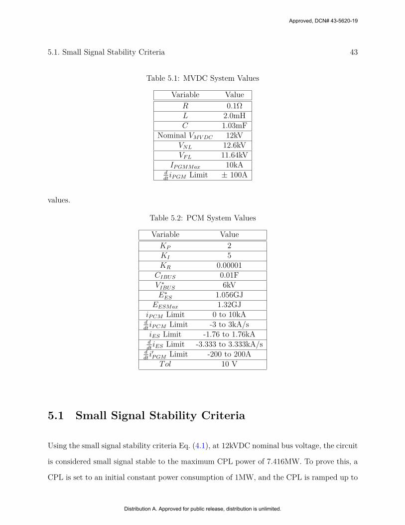
Using the small signal stability criteria Eq. (4.1), at 12kVDC nominal bus voltage, the circuit
is considered small signal stable to the maximum CPL power of 7.416MW. To prove this, a
CPL is set to an initial constant power consumption of 1MW, and the CPL is ramped up to
Approved, DCN# 43-5620-19
Distribution A. Approved for public release, distribution is unlimited.
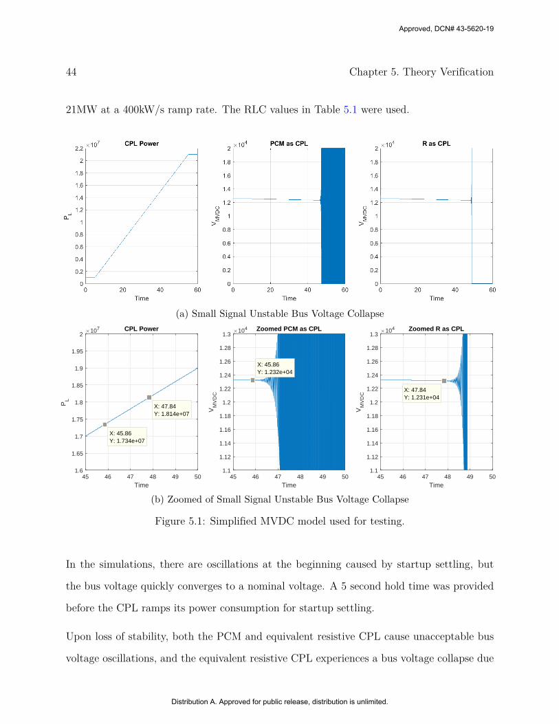
44 Chapter 5. Theory Verification
21MW at a 400kW/s ramp rate. The RLC values in Table 5.1 were used.
(a) Small Signal Unstable Bus Voltage Collapse
45 46 47 48 49 50
Time
1.6
1.65
1.7
1.75
1.8
1.85
1.9
1.95
2
PL
107 CPL Power
45 46 47 48 49 50
Time
1.1
1.12
1.14
1.16
1.18
1.2
1.22
1.24
1.26
1.28
1.3
VM
VD
C
104 Zoomed PCM as CPL
45 46 47 48 49 50
Time
1.1
1.12
1.14
1.16
1.18
1.2
1.22
1.24
1.26
1.28
1.3
VM
VD
C
104 Zoomed R as CPL
X: 45.86Y: 1.734e+07
X: 47.84Y: 1.814e+07
X: 45.86Y: 1.232e+04
X: 47.84Y: 1.231e+04
(b) Zoomed of Small Signal Unstable Bus Voltage Collapse
Figure 5.1: Simplified MVDC model used for testing.
In the simulations, there are oscillations at the beginning caused by startup settling, but
the bus voltage quickly converges to a nominal voltage. A 5 second hold time was provided
before the CPL ramps its power consumption for startup settling.
Upon loss of stability, both the PCM and equivalent resistive CPL cause unacceptable bus
voltage oscillations, and the equivalent resistive CPL experiences a bus voltage collapse due
Approved, DCN# 43-5620-19
Distribution A. Approved for public release, distribution is unlimited.
5.1. Small Signal Stability Criteria 45
to the loss of voltage stability. The PCM does not allow the bus voltage to collapse to
a steady zero, because the internal controller oscillates between its current limits, causing
the bus voltage oscillation to continue. From Fig. 5.1b, both CPLs lose voltage stability
above 18MW load power during power ramping. The PCM loses stability at a lower power
consumption than the equivalent resistor CPL. Nevertheless, both loads remain small signal
stable at a higher power level than the small signal criteria suggests. The bus voltage does
start above nominal voltage and droop down as intended, but this elevated bus voltage would
not cause a doubling of the small signal stable power ceiling. This shows that the criteria
underestimates when the system loses small signal stability for the chosen ramp rate. The
definition of a large and small signal perturbation is loose, so the chosen power ramp may
be a smaller small signal perturbation than expected.
The virtual stabilizer, if we ignore the RV term, will increase the overall bus capacitance
and dampen the system at with a higher load power. Relating it back to Eq. (4.1), it would
increase the C term, increasing the small signal stability power ceiling. This is because CV
is effectively a parallel capacitor to C. Realistically, the RC stabilizer allows a smaller added
CV term for stabilization, which is preferred as a higher CV results in more power used by
the virtual stabilizer as seen in Eq. (4.2).
To verify that the virtual capacitor can increase the small signal stability threshold, the power
ramp simulation was repeated with an RC stabilizer using the values in Table 5.3. The PCM
CPL used a virtual stabilizer and the equivalent resistor CPL used real RC components. The
new small signal stable power ceiling should be 14.616MW. The results are shown in Fig. 5.2.
Note that these values were not chosen to critically, over, or under damp the system but to
only increase the power ceiling for the stability criteria of Eq. (4.1).
The results show that the loads are stable for the entire 20MW ramp and that the added
stabilizer increased the small signal stable power ceiling. As noted before, Eq. (4.1) under-
Approved, DCN# 43-5620-19
Distribution A. Approved for public release, distribution is unlimited.

46 Chapter 5. Theory Verification
Table 5.3: Tested Virtual Damper Values
Variable ValueCV 0.001ΩRV 1.0mF
Figure 5.2: Compared Circuits for Step Response.
estimates for this scenario, so it was expected that both loads remained small signal stable
for the whole power ramp despite the 14.616MW power ceiling for stability.
The virtual and real RC stabilizer capacitor power were measured and shown in Fig. 5.3.
It is visible that in both real and virtual implementations, the capacitor is discharging the
same amount of power. The real capacitor’s power only rings when the voltage starts and
stops drooping, which is expected. Unexpectedly, the virtual capacitor’s power rings during
the continuous discharge outside the start and stop of the voltage droop. This shows that
the virtual and real capacitors behave in a similar but not equal manner.
The hardware-limited and raw virtual stabilizer capacitor current ICVwere measured. One
of the oscillation points was zoomed in and shown in Fig. 5.4. The resulting graph appears
blocky as the simulation uses a maximum timestep of 10 µs with zoomed 0.7 ms time range.
Since the PCM power converter is assumed to be switching at 10kHz, the simulation time
Approved, DCN# 43-5620-19
Distribution A. Approved for public release, distribution is unlimited.

5.1. Small Signal Stability Criteria 47
0 10 20 30 40 50 60
Time
-400
-300
-200
-100
0
100
200
300
400
Pow
er
Virtual Vs Real RC Stabilier Power
Virtual RC StabilizerReal RC Stabilizer
Figure 5.3: Compared Real and Virtual RC Stabilizer Power.
step is 10 times finer than what a real converter can output, so the noticeable simulation
stepping can be ignored. The results show that the hardware limitations are barely causing
a change in the actual ICVfrom the raw ICV
. Also, note that the virtual stabilizer’s RC
time constant frequency is 16kHz, which is not realistically feasible for a 10kHz converter
to accurately emulate, but this simulation is only for behavioral verification purposes. A
critically or over damp-system will not have such a tiny RC stabilizer time constant.
The virtual RC stabilizer current was compared with the PCM’s ES current to confirm that
the ES canceled out the virtual stabilizer’s fluctuations on the PCM’s internal DC bus.
The results are shown in Fig. 5.5. The ES does have a negative current compensating for
the stabilizer’s fluctuations. The other components of the ES’s current waveform are for
maintaining the internal DC bus voltage and later on recharging the ES.
Approved, DCN# 43-5620-19
Distribution A. Approved for public release, distribution is unlimited.

48 Chapter 5. Theory Verification
Figure 5.4: Compared Raw and Hardware Limited Virtual Stabilizer Currents.
Figure 5.5: PCM ES Cancels the Virtual Stabilizer’s Fluctuations.
Approved, DCN# 43-5620-19
Distribution A. Approved for public release, distribution is unlimited.

5.2. Equivalent Circuit Validation 49
5.2 Equivalent Circuit Validation
As the previous results show, the PCM and equivalent resistor CPL do not exactly agree in
behavior. The equivalent circuit of a CPL with the stabilizer must closely model the PCM
and virtual stabilizer system. This is to ensure that the equivalent circuit can actually be
used for analysis. However, as the virtual stabilizer was modeled to behave similarly to a
RC arm parallel to the load, it should be expected that both real and virtual parallel RC
dampeners are still similar in behavior. The PCM has extra limitations and features over
the equivalent resistance CPL that causes the behavior to diverge. This divergence should
be in the PCM’s favor as the PCM will inhibit unstable effects from large signals.
To compare the behaviors of the PCM and real resistor CPL along with virtual and real RC
dampers, step responses of each system were simulated. The RLC values from Table 5.1 are
used as done before. The virtual and real stabilizers are still using the values from Table 5.3.
These values are known to under-damp the system by low-Q approximation, which will
shown later in Section 5.4. An under-damp system was chosen to make oscillations visible
to detect any phase shifts in the step responses
Recall that the PCM has a virtual limit on the load power ramp transmitted to the MVDC
bus to mimic the MVDC generator’s ramp rate limitation. The virtual ramp rate limit is
1.2MW/s before the ES in the PCM will provide large signal stability compensation. The
equivalent R load will not exhibit this behavior as it does not have internal ES. Therefore,
the CPL step signal must not trigger the PCM’s ES when comparing the systems. The load
power step used in this test is from 1.000MW to 1.0012MW in 1ms, providing a ramp rate of
1.2MW/s. This way, the power consumption from the MVDC bus by the two load systems
should be close to equal.
Shown in Fig. 5.6, these separate circuits were simulated simultaneously: equivalent R with
Approved, DCN# 43-5620-19
Distribution A. Approved for public release, distribution is unlimited.

50 Chapter 5. Theory Verification
real RC stabilizer, PCM with real RC stabilizer, and PCM with virtual RC stabilizer. The
results of this simulation is shown in Fig. 5.7.
Figure 5.6: Compared Circuits for Step Response.
4.95 5 5.05 5.1 5.15
1.258432
1.258434
1.258436
1.258438
1.25844
1.258442
1.258444
1.258446
1.258448
VM
VD
C
104
1
1.0002
1.0004
1.0006
1.0008
1.001
1.0012
PL
106
R CPL, Real RCPCM CPL, Real RCPCM CPL, Virtual RCPower Step
Figure 5.7: Step Responses to 1.2kW 1ms Step.
There is a no noticeable phase shift and mostly a magnitude error between all of the re-
sponses. The PCM and equivalent resistance CPLs appear to have equal step responses
Approved, DCN# 43-5620-19
Distribution A. Approved for public release, distribution is unlimited.

5.2. Equivalent Circuit Validation 51
when both use a real RC stabilizer, but the virtual and real RC stabilizers have a more
noticeable magnitude error when using a PCM CPL. This magnitude error gives the virtual
RC stabilizer a greater advantage as the bus voltage settles quicker, and the oscillation itself
has a lower magnitude. Direct voltage magnitude error comparisons were made in Fig. 5.8.
The small millivolt errors between each system should be negligible. To further emphasize
how tiny the errors are: the V/W ratio of the peak errors for a 1.2kW step is approximately
6.7µVW
for Fig. 5.8a and 12.5µVW
for Fig. 5.8b. The errors scaled to a 1MW step would be 6.7V
for Fig. 5.8a and 12.5V for Fig. 5.8b, which is less than 0.2% of the nominal bus voltage.
However, a 1MW at 1ms would result in a 100MW/s ramp rate, which is unrealistic for the
generator to support.
The magnitude errors exists because the virtual RC stabilizer is minutely affected by the
physical limitations on the PCM’s power and ramp rates. The magnitude error can be
considered an advantage to the virtual RC stabilizer as the oscillations would have lower
magnitude. With no phase shift and very tiny magnitude errors, all 3 models are fairly
equivalent, and should introduce little errors in using the equivalent circuit for further anal-
ysis.
Approved, DCN# 43-5620-19
Distribution A. Approved for public release, distribution is unlimited.
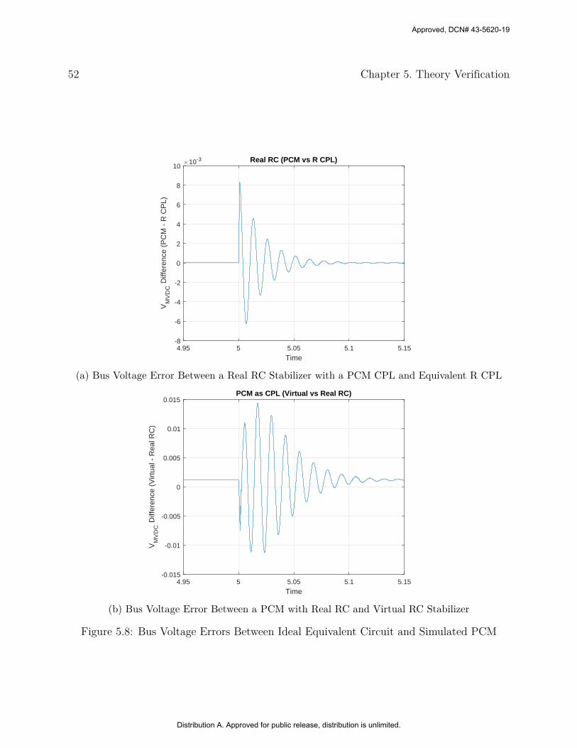
52 Chapter 5. Theory Verification
4.95 5 5.05 5.1 5.15
Time
-8
-6
-4
-2
0
2
4
6
8
10V
MV
DC
Diff
eren
ce (
PC
M -
R C
PL)
10-3 Real RC (PCM vs R CPL)
(a) Bus Voltage Error Between a Real RC Stabilizer with a PCM CPL and Equivalent R CPL
4.95 5 5.05 5.1 5.15
Time
-0.015
-0.01
-0.005
0
0.005
0.01
0.015
VM
VD
C D
iffer
ence
(V
irtua
l - R
eal R
C)
PCM as CPL (Virtual vs Real RC)
(b) Bus Voltage Error Between a PCM with Real RC and Virtual RC Stabilizer
Figure 5.8: Bus Voltage Errors Between Ideal Equivalent Circuit and Simulated PCM
Approved, DCN# 43-5620-19
Distribution A. Approved for public release, distribution is unlimited.
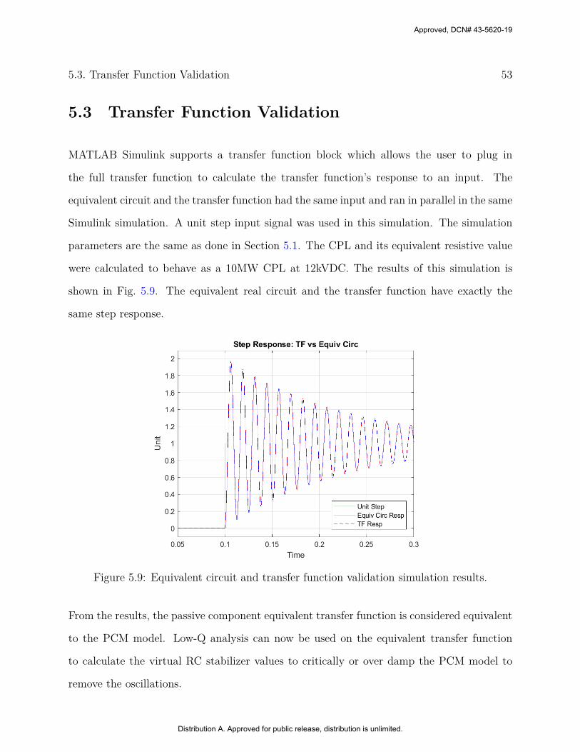
5.3. Transfer Function Validation 53
5.3 Transfer Function Validation
MATLAB Simulink supports a transfer function block which allows the user to plug in
the full transfer function to calculate the transfer function’s response to an input. The
equivalent circuit and the transfer function had the same input and ran in parallel in the same
Simulink simulation. A unit step input signal was used in this simulation. The simulation
parameters are the same as done in Section 5.1. The CPL and its equivalent resistive value
were calculated to behave as a 10MW CPL at 12kVDC. The results of this simulation is
shown in Fig. 5.9. The equivalent real circuit and the transfer function have exactly the
same step response.
Figure 5.9: Equivalent circuit and transfer function validation simulation results.
From the results, the passive component equivalent transfer function is considered equivalent
to the PCM model. Low-Q analysis can now be used on the equivalent transfer function
to calculate the virtual RC stabilizer values to critically or over damp the PCM model to
remove the oscillations.
Approved, DCN# 43-5620-19
Distribution A. Approved for public release, distribution is unlimited.
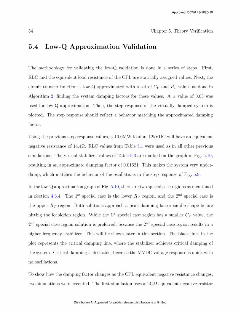
54 Chapter 5. Theory Verification
5.4 Low-Q Approximation Validation
The methodology for validating the low-Q validation is done in a series of steps. First,
RLC and the equivalent load resistance of the CPL are statically assigned values. Next, the
circuit transfer function is low-Q approximated with a set of CV and RL values as done in
Algorithm 2, finding the system damping factors for these values. A α value of 0.05 was
used for low-Q approximation. Then, the step response of the virtually damped system is
plotted. The step response should reflect a behavior matching the approximated damping
factor.
Using the previous step response values, a 10.0MW load at 12kVDC will have an equivalent
negative resistance of 14.4Ω. RLC values from Table 5.1 were used as in all other previous
simulations. The virtual stabilizer values of Table 5.3 are marked on the graph in Fig. 5.10,
resulting in an approximate damping factor of 0.01621. This makes the system very under-
damp, which matches the behavior of the oscillations in the step response of Fig. 5.9.
In the low-Q approximation graph of Fig. 5.10, there are two special case regions as mentioned
in Section 4.3.4. The 1st special case is the lower RV region, and the 2nd special case is
the upper RV region. Both solutions approach a peak damping factor saddle shape before
hitting the forbidden region. While the 1st special case region has a smaller CV value, the
2nd special case region solution is preferred, because the 2nd special case region results in a
higher frequency stabilizer. This will be shown later in this section. The black lines in the
plot represents the critical damping line, where the stabilizer achieves critical damping of
the system. Critical damping is desirable, because the MVDC voltage response is quick with
no oscillations.
To show how the damping factor changes as the CPL equivalent negative resistance changes,
two simulations were executed. The first simulation uses a 144Ω equivalent negative resistor
Approved, DCN# 43-5620-19
Distribution A. Approved for public release, distribution is unlimited.

5.4. Low-Q Approximation Validation 55
Figure 5.10: Low-Q Approximated Damping Factors for 10MW CPL (RL = 14.4Ω)
for a CPL of 1MW at 12kVDC CPL, and the results are shown in Fig. 5.11a. The second
simulation uses a 1.44Ω equivalent negative resistor for a CPL of 100MW at 12kVDC CPL,
and the results are shown in Fig. 5.11b.
We can see that the critical damping lines squeeze into the overdamping saddle as the CPL’s
equivalent negative resistance shrinks. This shows that: to prevent oscillations, one must
either over-damp when the CPL is at low power consumption or dynamically tune the virtual
stabilizer to maintain a quick critical damping. Also, a negative damping factor appears at
100MW CPL, showing that certain virtual damping values causes the MVDC bus voltage
to diverge.
Values for the virtual stabilizer were picked from Fig. 5.11b. The chosen points are shown
in Fig. 5.12 and listed in Table 5.4. One set of values were picked from the 1st special case
solution and another set were picked from the 2nd special case.
Approved, DCN# 43-5620-19
Distribution A. Approved for public release, distribution is unlimited.
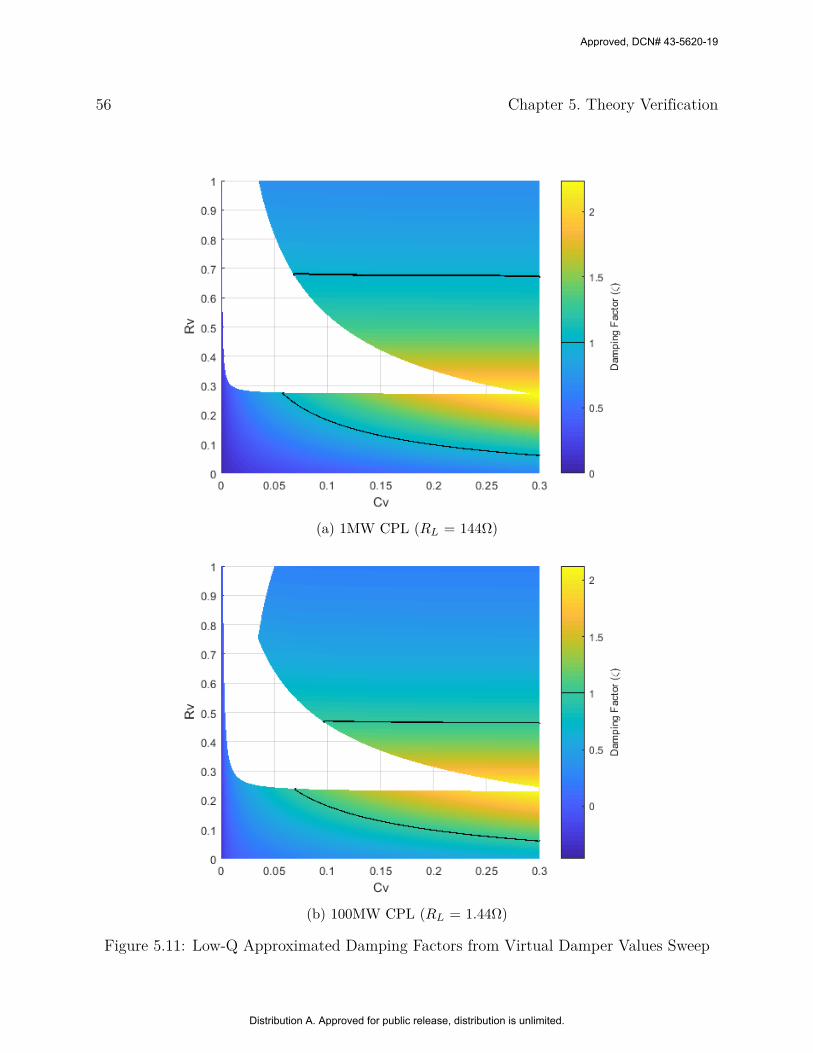
56 Chapter 5. Theory Verification
(a) 1MW CPL (RL = 144Ω)
(b) 100MW CPL (RL = 1.44Ω)
Figure 5.11: Low-Q Approximated Damping Factors from Virtual Damper Values Sweep
Approved, DCN# 43-5620-19
Distribution A. Approved for public release, distribution is unlimited.

5.4. Low-Q Approximation Validation 57
Figure 5.12: Selected Test Points for 100MW CPL (RL = 1.44Ω)
The step response of each of the chosen points in Table 5.4 are shown in Fig. 5.13 and
Fig. 5.14. The step responses were generated using the actual transfer function, exhibiting the
actual system behavior rather than approximating it. The under-damp systems do exhibit
overshoot or slight oscillation. The critically damp systems do not overshoot drastically or
oscillate. The overdamp systems generally have slower rise times. The unit step responses
do not converge towards 1 due to the resistive terms from the MVDC bus forming a voltage
divider. The divider causes a voltage rise rather than a voltage drop due to the CPL’s
Approved, DCN# 43-5620-19
Distribution A. Approved for public release, distribution is unlimited.
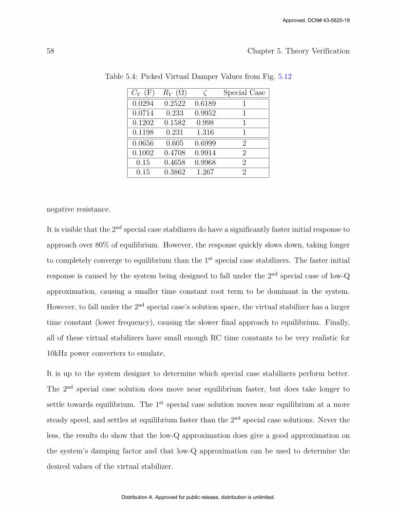
58 Chapter 5. Theory Verification
Table 5.4: Picked Virtual Damper Values from Fig. 5.12
CV (F) RV (Ω) ζ Special Case0.0294 0.2522 0.6189 10.0714 0.233 0.9952 10.1202 0.1582 0.998 10.1198 0.231 1.316 10.0656 0.605 0.6999 20.1002 0.4708 0.9914 20.15 0.4658 0.9968 20.15 0.3862 1.267 2
negative resistance.
It is visible that the 2nd special case stabilizers do have a significantly faster initial response to
approach over 80% of equilibrium. However, the response quickly slows down, taking longer
to completely converge to equilibrium than the 1st special case stabilizers. The faster initial
response is caused by the system being designed to fall under the 2nd special case of low-Q
approximation, causing a smaller time constant root term to be dominant in the system.
However, to fall under the 2nd special case’s solution space, the virtual stabilizer has a larger
time constant (lower frequency), causing the slower final approach to equilibrium. Finally,
all of these virtual stabilizers have small enough RC time constants to be very realistic for
10kHz power converters to emulate.
It is up to the system designer to determine which special case stabilizers perform better.
The 2nd special case solution does move near equilibrium faster, but does take longer to
settle towards equilibrium. The 1st special case solution moves near equilibrium at a more
steady speed, and settles at equilibrium faster than the 2nd special case solutions. Never the
less, the results do show that the low-Q approximation does give a good approximation on
the system’s damping factor and that low-Q approximation can be used to determine the
desired values of the virtual stabilizer.
Approved, DCN# 43-5620-19
Distribution A. Approved for public release, distribution is unlimited.
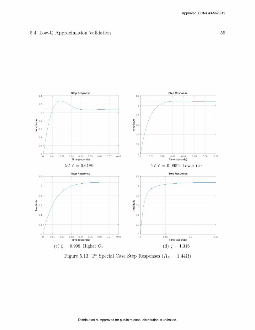
5.4. Low-Q Approximation Validation 59
0 0.01 0.02 0.03 0.04 0.05 0.06 0.07 0.080
0.2
0.4
0.6
0.8
1
1.2
1.4Step Response
Time (seconds)
Am
plitu
de
(a) ζ = 0.6189
0 0.01 0.02 0.03 0.04 0.05 0.06 0.070
0.2
0.4
0.6
0.8
1
1.2Step Response
Time (seconds)
Am
plitu
de
(b) ζ = 0.9952, Lower CV
0 0.01 0.02 0.03 0.04 0.05 0.06 0.07 0.080
0.2
0.4
0.6
0.8
1
1.2Step Response
Time (seconds)
Am
plitu
de
(c) ζ = 0.998, Higher CV
0 0.05 0.1 0.150
0.2
0.4
0.6
0.8
1
1.2Step Response
Time (seconds)
Am
plitu
de
(d) ζ = 1.316
Figure 5.13: 1st Special Case Step Responses (RL = 1.44Ω)
Approved, DCN# 43-5620-19
Distribution A. Approved for public release, distribution is unlimited.
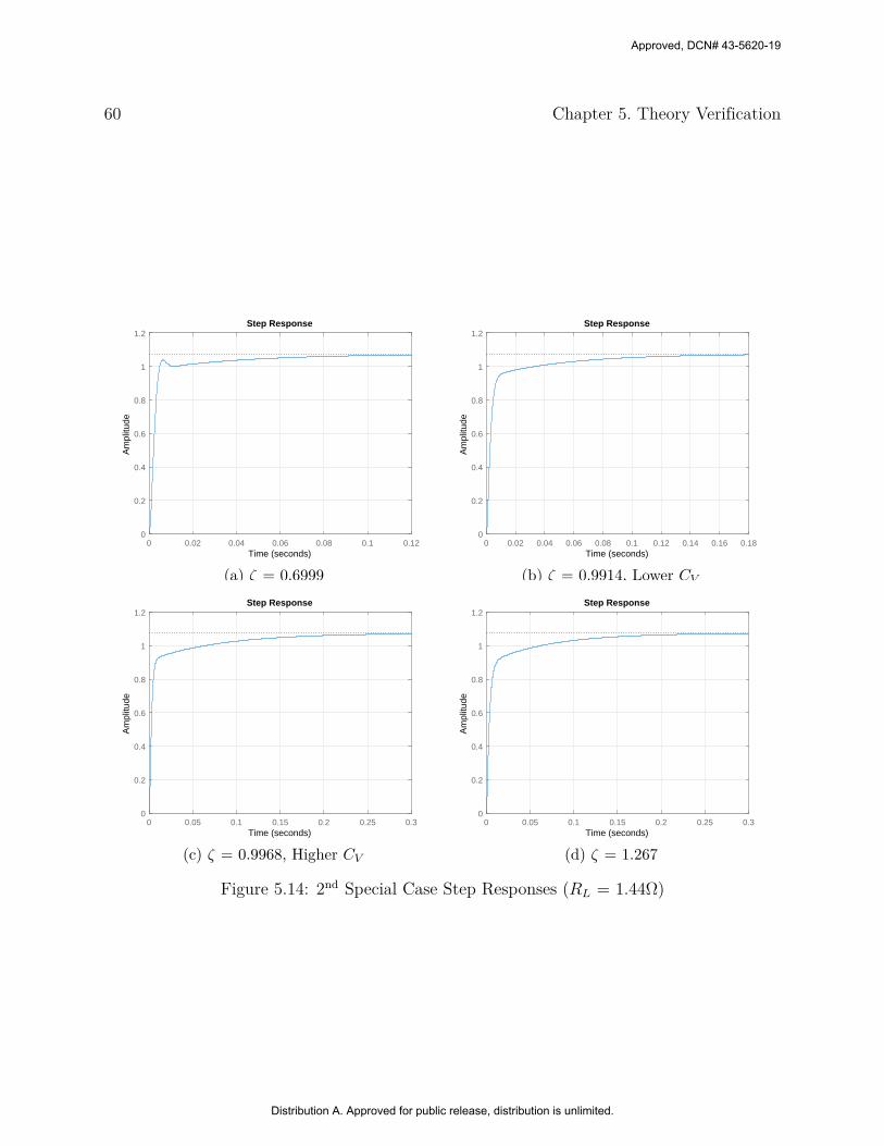
60 Chapter 5. Theory Verification
0 0.02 0.04 0.06 0.08 0.1 0.120
0.2
0.4
0.6
0.8
1
1.2Step Response
Time (seconds)
Am
plitu
de
(a) ζ = 0.6999
0 0.02 0.04 0.06 0.08 0.1 0.12 0.14 0.16 0.180
0.2
0.4
0.6
0.8
1
1.2Step Response
Time (seconds)
Am
plitu
de
(b) ζ = 0.9914, Lower CV
0 0.05 0.1 0.15 0.2 0.25 0.30
0.2
0.4
0.6
0.8
1
1.2Step Response
Time (seconds)
Am
plitu
de
(c) ζ = 0.9968, Higher CV
0 0.05 0.1 0.15 0.2 0.25 0.30
0.2
0.4
0.6
0.8
1
1.2Step Response
Time (seconds)
Am
plitu
de
(d) ζ = 1.267
Figure 5.14: 2nd Special Case Step Responses (RL = 1.44Ω)
Approved, DCN# 43-5620-19
Distribution A. Approved for public release, distribution is unlimited.

5.5. Dynamic Tuning Validation 61
5.5 Dynamic Tuning Validation
A shown in Section 4.3.4, the virtual stabilizer can be dynamically tuned. A lookup table
can be generated to store each CV value for each RL operating point, and RV would be
calculated from the previous two values. To validate the dynamic tuning method, a set of
CV and RV values were calculated to a corresponding RL value, and the virtual stabilizer
values should match the brute forces values in Fig. 5.15. In this validation process, the
system values from Table 5.1 were used with a target damping factor of 1.1 and only using
the 1st low-Q approximation special case with a α of 0.05. A target damping factor of 1.1
was chosen. Slight over-damping was chosen instead of critical damping to ensure the system
is never slightly under-damp due to low-Q approximation error.
To solve RV (CV , RL) for Algorithm 3, Eq. (4.18) was set equal to the target damping factor
of 1.1. Eq. (4.24) would be used if the 2nd special case solution region was used instead.
Using MATLAB’s solve operator to solve for RV , the resulting analytic equation for RV is
RV (CV , RL) =71L− 71CRRL + 50CVRRL ± 11A
50(CVR− CVRL),
A =√
21C2R2R2L − 142CLRRL + 100CLR2
L − 100CVCR2R2L + 21L2 + 100CVLR2
L.
(5.1)
Note that there is a plus-minus square root in Eq. (5.1), and one must plug in a set of valid
real values to find whether the square root term must be added or subtracted to result in a
valid positive solution. The RLC values were plugged into Eq. (5.1), and the CV (RL) look
up table was solved using Algorithm 3. The resulting tuning values for the virtual stabilizer
are shown in Fig. 5.16. Comparison between the low-Q approximation brute forced expected
values and the actual analytically solved low-Q approximation values are shown in Table 5.5.
Approved, DCN# 43-5620-19
Distribution A. Approved for public release, distribution is unlimited.
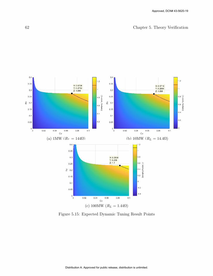
62 Chapter 5. Theory Verification
(a) 1MW (RL = 144Ω) (b) 10MW (RL = 14.4Ω)
(c) 100MW (RL = 1.44Ω)
Figure 5.15: Expected Dynamic Tuning Result Points
Approved, DCN# 43-5620-19
Distribution A. Approved for public release, distribution is unlimited.

5.5. Dynamic Tuning Validation 63
Overall, the calculated values of the virtual stabilizer have little error from the brute forced
values for maintaining a 1.1 damping factor. This validates that the methodology for solving
the dynamic tuning values using is accurate and correct.
100 101 102 103 104 105 106
Rl
0.07
0.072
0.074
0.076
0.078
0.08
0.082
0.084
0.086
0.088
0.09
Cv
0.22
0.23
0.24
0.25
0.26
0.27
0.28
0.29
Rv
X: 1.44Y: 0.08366
X: 1.44Y: 0.2362
X: 14.39Y: 0.2695
X: 144Y: 0.2733
X: 14.39Y: 0.072 X: 144
Y: 0.07085
Figure 5.16: Virtual Stabilizer Dynamic Tuning Values for ζ = 1.1
Table 5.5: Brute Forced and Analytically Solved Virtual Stabilizer Dynamic Tuning Values
Brute Forced SolvedRL (Ω) Damping Factor (ζ) RV (Ω) CV (F) RV (Ω) CV (F)
144 1.096 0.2732 0.0704 0.2733 0.070914.4 1.098 0.2694 0.0718 0.2695 0.07201.44 1.100 0.2360 0.0838 0.2362 0.0837
Approved, DCN# 43-5620-19
Distribution A. Approved for public release, distribution is unlimited.
Chapter 6
Results
With the modeling and approximation theory verified, the virtually stabilized PCM can be
simulated with a pulsed load. MATLAB and Simulink were used for generating these results.
The same system parameters in Table 5.1 Table 5.2 were used. The CPL will have a baseline
2MW constant power load, and a pulse load applying a pulse train with 258MJ of energy
per pulse at 4 pulses per minute. The pulse train will have 5 pulses, and each pulse is 10
seconds long with a 5 second baseline power load period between each pulse. The pulse will
ramp up and down at 10.75MW/s for 4 seconds both ways, holding its peak load of 43MW
for 2 seconds per pulse. The pulse train begins after a 5 second idle time for the simulator
to settle any simulation start up fluctuations.
A system without the virtual stabilizer was first used to show that the system is not small
signal stable as the PCM’s load power on the MVDC bus goes up. The results are shown in
Fig. 6.1. The MVDC bus voltage droops up and down with the pulse, but the overall bus
voltage droops more after each pulse due to the ES ramping up its recharge power. This
causes the PCM to progressively draw more power from the MVDC bus after each pulse.
The MVDC bus voltage does begin to oscillate during the 3rd pulse, but the bus voltage
recovers as the PCM’s load power on the MVDC bus decreases. However, the MVDC bus
voltage oscillates and loses control during the 4th pulse.
To show what the proper behavior of the system should be, the virtual stabilizer was added
using statically assigned values from Table 5.5. CV = 0.0837 and RV = 0.2362 for a 1.1
64
Approved, DCN# 43-5620-19
Distribution A. Approved for public release, distribution is unlimited.

65
Figure 6.1: Pulse Train Without Stabilizer - Bus Voltages
damping factor when a 100MW is loaded on the MVDC bus was used. The bus voltages
with the virtual stabilizer is shown in Fig. 6.2, and the currents of the PCM components at
VIBUS is shown in Fig. 6.3. The MVDC bus voltage never oscillates during the pulse train,
showing it is small signal stable. The PCM ES SoC and actual energy is shown in Fig. 6.4.
This shows ES compensating the large power swings of the pulsed load and recharging after
the pulse train.
Figure 6.2: Pulse Train With Statically Tuned Virtual Stabilizer - Bus Voltages
The power of the hardware-limited virtual stabilizer is shown in Fig. 6.5. Virtual stabilizer
Approved, DCN# 43-5620-19
Distribution A. Approved for public release, distribution is unlimited.
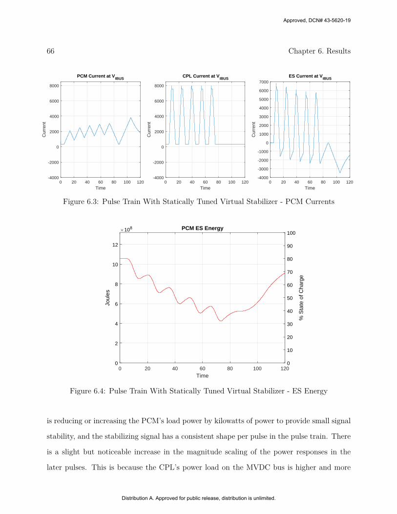
66 Chapter 6. Results
0 20 40 60 80 100 120
Time
-4000
-2000
0
2000
4000
6000
8000
Cur
rent
PCM Current at VIBUS
0 20 40 60 80 100 120
Time
-4000
-2000
0
2000
4000
6000
8000
Cur
rent
CPL Current at VIBUS
0 20 40 60 80 100 120
Time
-4000
-3000
-2000
-1000
0
1000
2000
3000
4000
5000
6000
7000
Cur
rent
ES Current at VIBUS
Figure 6.3: Pulse Train With Statically Tuned Virtual Stabilizer - PCM Currents
0 20 40 60 80 100 120
Time
0
2
4
6
8
10
12
Joul
es
108
0
10
20
30
40
50
60
70
80
90
100
% S
tate
of C
harg
e
PCM ES Energy
Figure 6.4: Pulse Train With Statically Tuned Virtual Stabilizer - ES Energy
is reducing or increasing the PCM’s load power by kilowatts of power to provide small signal
stability, and the stabilizing signal has a consistent shape per pulse in the pulse train. There
is a slight but noticeable increase in the magnitude scaling of the power responses in the
later pulses. This is because the CPL’s power load on the MVDC bus is higher and more
Approved, DCN# 43-5620-19
Distribution A. Approved for public release, distribution is unlimited.

67
destabilizing, and the stabilizer needs to scale the stabilizing response up to compensate.
0 20 40 60 80 100 120
Time
-12
-10
-8
-6
-4
-2
0
2
4
6
Pow
er104 PCM Virutal Stabilizer Power
Figure 6.5: Statically Tuned Virtual Stabilizer Power
Next, the same pulse train simulation and system parameters were simulated with the virtual
stabilizer using dynamic tuning values found in Section 5.5 for a 1.1 damping factor. The
bus voltages are shown in Fig. 6.6, and the MVDC bus voltage is still stable. The internal
PCM currents are shown in Fig. 6.7, which appears similar to the statically tuned virtual
stabilizer. The energy of the ES, shown in Fig. 6.8 is also similar.
The power of the dynamically tuned virtual stabilizer is shown in Fig. 6.9. The stabilizer
is much more noisy than the statically tuned one. However, the dynamically tuned stabi-
lizer does use marginally less power than the statically tuned one. The measured RL and
dynamically tuned CV and RV values are shown in Fig. 6.10.
Approved, DCN# 43-5620-19
Distribution A. Approved for public release, distribution is unlimited.
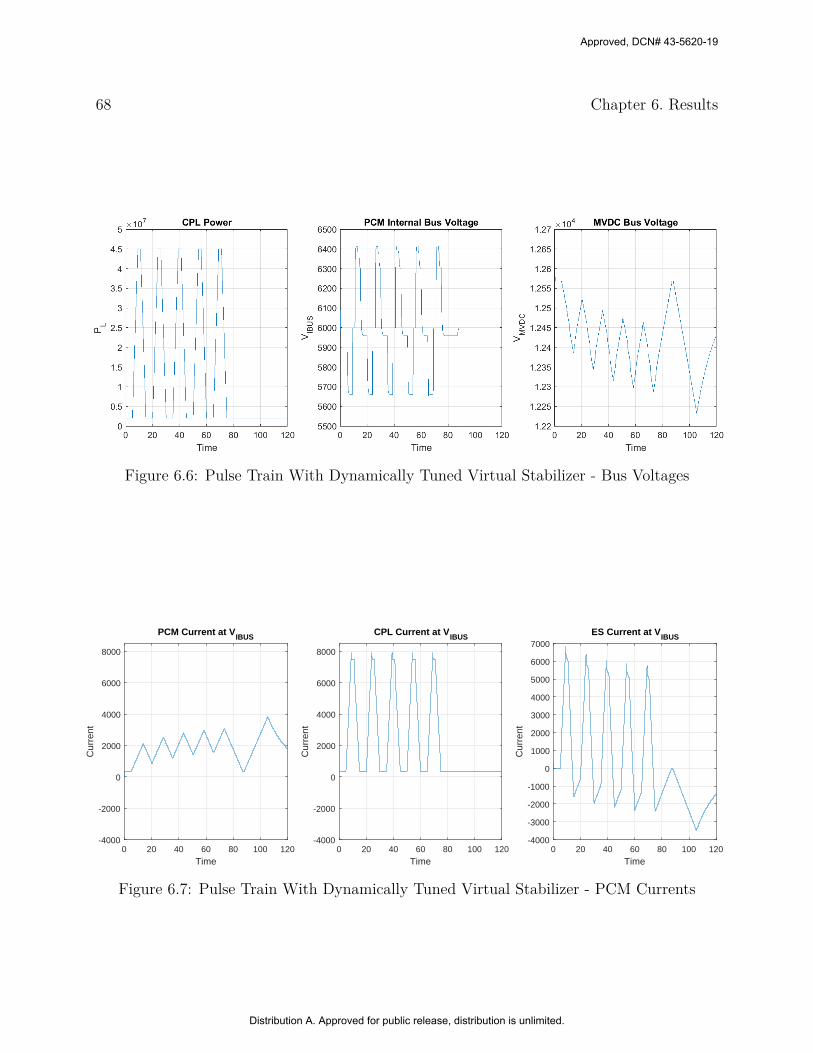
68 Chapter 6. Results
Figure 6.6: Pulse Train With Dynamically Tuned Virtual Stabilizer - Bus Voltages
0 20 40 60 80 100 120
Time
-4000
-2000
0
2000
4000
6000
8000
Cur
rent
PCM Current at VIBUS
0 20 40 60 80 100 120
Time
-4000
-2000
0
2000
4000
6000
8000
Cur
rent
CPL Current at VIBUS
0 20 40 60 80 100 120
Time
-4000
-3000
-2000
-1000
0
1000
2000
3000
4000
5000
6000
7000
Cur
rent
ES Current at VIBUS
Figure 6.7: Pulse Train With Dynamically Tuned Virtual Stabilizer - PCM Currents
Approved, DCN# 43-5620-19
Distribution A. Approved for public release, distribution is unlimited.
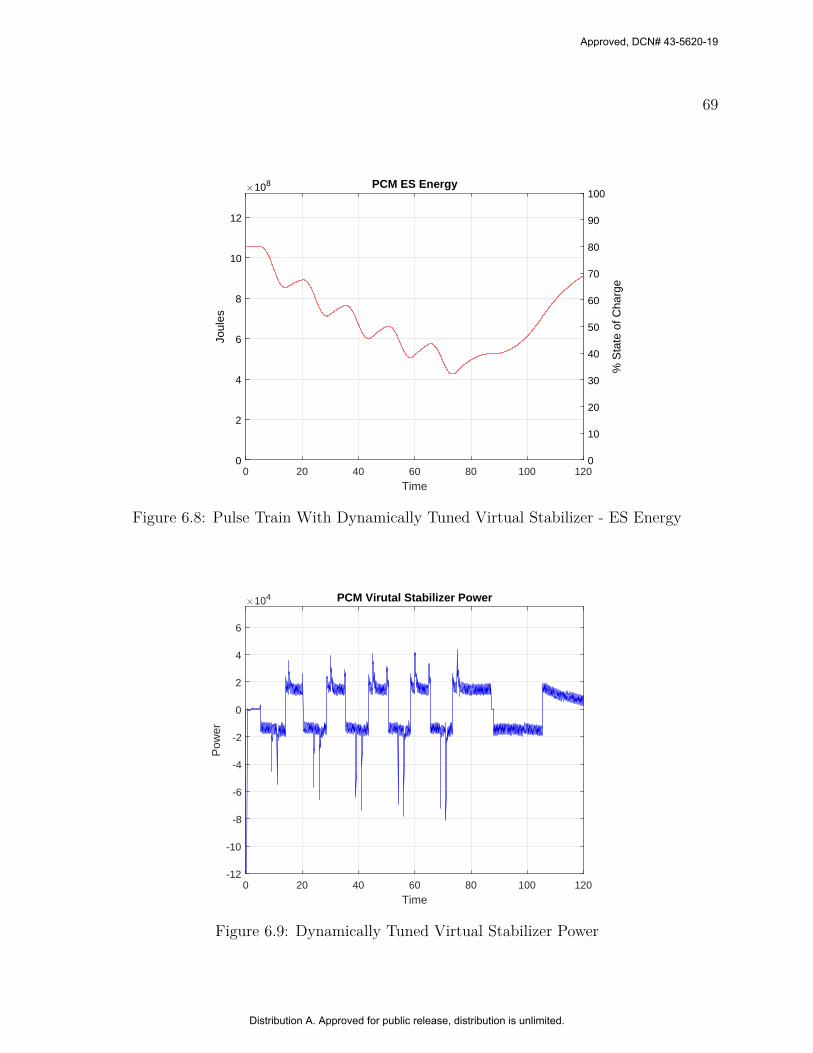
69
0 20 40 60 80 100 120
Time
0
2
4
6
8
10
12Jo
ules
108
0
10
20
30
40
50
60
70
80
90
100
% S
tate
of C
harg
e
PCM ES Energy
Figure 6.8: Pulse Train With Dynamically Tuned Virtual Stabilizer - ES Energy
0 20 40 60 80 100 120
Time
-12
-10
-8
-6
-4
-2
0
2
4
6
Pow
er
104 PCM Virutal Stabilizer Power
Figure 6.9: Dynamically Tuned Virtual Stabilizer Power
Approved, DCN# 43-5620-19
Distribution A. Approved for public release, distribution is unlimited.
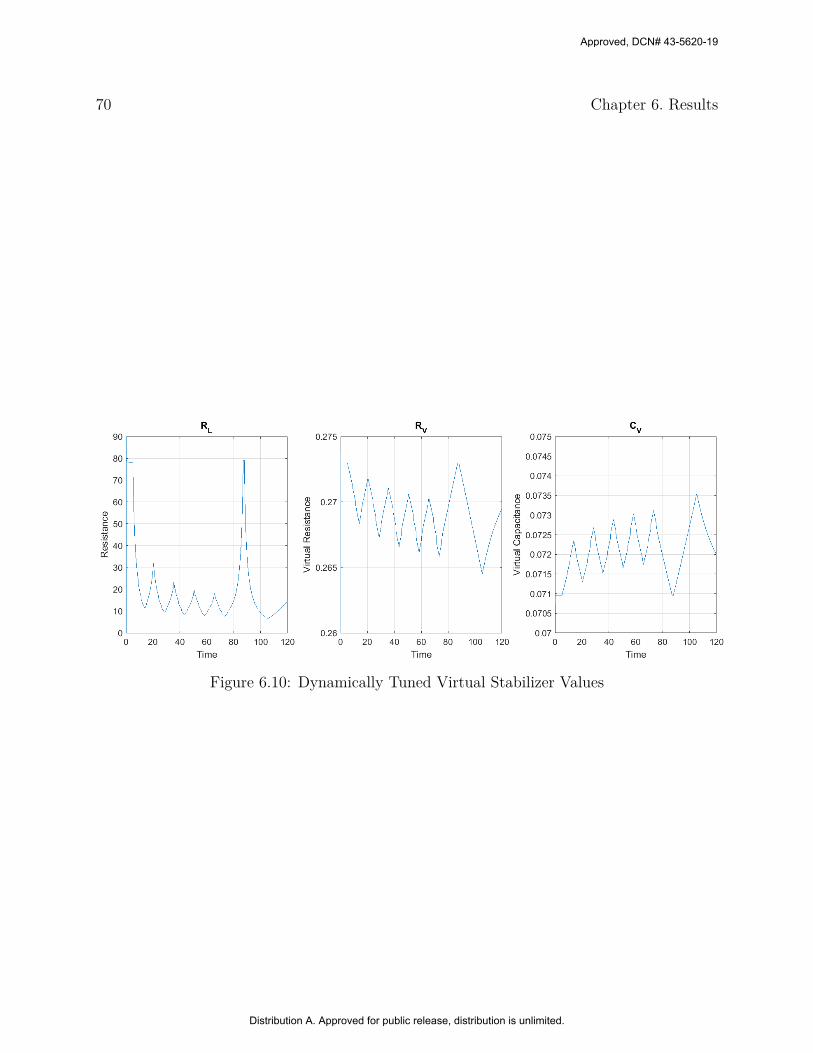
70 Chapter 6. Results
Figure 6.10: Dynamically Tuned Virtual Stabilizer Values
Approved, DCN# 43-5620-19
Distribution A. Approved for public release, distribution is unlimited.

Chapter 7
Discussion and Future Work
From the validation work, the virtual and real RC small signal stabilizers do not exhibit
exactly the same behavior. However, the negative load virtual stabilizer still provides small
signal stabilization. From the results, the virtual stabilizer can provide MVDC bus small
signal stabilization while a pulsed CPL is running a pulsed train. The modified control
loops in this thesis performed well despite the fact that the original control loops were not
developed or tested for pulsed power loads [6, 17]. The modified control loops provided the
needed pulsed power in a stable manner while maintaining the ES adequately and following
hardware ramp rate limitations.
The virtual stabilizer does not introduce enough power fluctuations to greatly impact the
power quality to the downstream load compared to the overall CPL’s power consumption.
Also, the power is low enough that the stabilizer can simply run with statically tuned values.
The dynamically tuned stabilizer does have a smaller power fluctuation compared to the
statically tuned stabilizer, but it is a very small difference compared to the CPL’s power
consumption. Also, the RL feedback causes noise on the dynamically tuned stabilizer’s power
fluctuations.
When zoomed in, there are very tiny oscillations on the RL signal, because the MVDC bus
voltage is has tiny noise caused by the MVDC system dynamics, causing the RL signal to
oscillate. However, with the MVDC bus voltage noise feeding into the dynamic tuning loop
of the virtual stabilizer, the output stabilizer values also contains this noise, causing the
71
Approved, DCN# 43-5620-19
Distribution A. Approved for public release, distribution is unlimited.

72 Chapter 7. Discussion and Future Work
stabilizer power fluctuations to also have the noise. This noise is added into the PCM power
consumption from the MVDC bus, which causes further MVDC bus voltage noise. The
system is damp enough where this small signal noise does not cause the MVDC bus voltage
to fluctuate out of control, and the ES does adequately cancel the fluctuation noise on the
internal DC bus. However, the noise on the virtual stabilizer power is undesirable as it lowers
power quality and puts more stress on the MVDC bus facing power converter in the PCM.
Compared to a real RC stabilizer, the virtual stabilizer does eliminate power losses across
the resistor when the capacitor charges or discharges. Also, since the whole virtual stabilizer
system uses existing components, there is ample space and weight saving. A capacitance
of 83.7mF, used in the statically tuned stabilizer, rated for 12kV usage would at least store
6MJ of energy. However, the capacitor would normally be rated for a much higher voltage
for safety reasons. From [3], a 6MJ capacitor will have an estimated volume of 6 m2 and
mass of 7380kg. The resistor will also take up space and tonnage. Also, the components
may need some cooling and wiring hardware, consuming even more tonnage and space.
In the future, the dynamic tuning control loop could be improved to filter out the retuning
noise. Also, the reduced MVDC system could be expanded with a parallel PCM or employ
realistic generators and switching power converters. With a parallel load, the MVDC system
has an increased complexity and a higher order transfer function. It should be investigated
how well low-Q approximation enables system designers to calculate system damping factors
for a scaled complexity. Finally, the control loop proportional and integrator loops could be
refined or mathematically modeled for improved tuning. The MATLAB Simulink code used
in these simulations are available in Appendix A.
Approved, DCN# 43-5620-19
Distribution A. Approved for public release, distribution is unlimited.

Chapter 8
Conclusions
A controls system was successfully implemented for a pulsed power load prototype. This
controls system handles auxiliary pulsed load hardware, PFN charging and discharging, and
data acquisition. Due to the optimization work done, it is capable of operating the PFN to
generate very precise pulse waveforms for experimental purposes.
Then, a PCM control system supporting a virtual negative load small signal stabilizer was
developed for a MVDC system with a large pulsed load. The PCM control loops manage the
PCM’s internal DC bus voltage and ES adequately for pulsed loads. The ES is recharged
after buffering the large power swings of the pulsed load within an acceptable amount of
time. The virtual stabilizer has been proven to increase the small signal stable power range
of a reduced MVDC system. A methodology was developed in tuning the virtual stabilizer,
and the control loop uses the ES to cancel the stabilizer’s power fluctuations. The stabilizer
can also be on-line dynamically tuned, minimizing the stabilizer’s power signal.
Dynamic tuning of the negative load virtual stabilizer did not perform as well as expected as
it introduced more noise than a statically tuned stabilizer. However, the dynamically tuned
stabilizer does have a reduced magnitude in its power fluctuations as expected. Overall, the
power fluctuations of the virtual stabilizer is small enough that dynamic tuning may not be
required. As predicted, both virtual stabilizers did increase the small signal stability range
of the system using existing components rather than adding additional real hardware.
73
Approved, DCN# 43-5620-19
Distribution A. Approved for public release, distribution is unlimited.
Bibliography
[1] Ieee standard for power electronics open system interfaces in zonal electrical distribution
systems rated above 100 kw. IEEE Std 1826-2012, pages 1–46, 2012. doi: 10.1109/
IEEESTD.2012.6225387.
[2] M. Belkhayat, R. Cooley, and A. Witulski. Large signal stability criteria for distributed
systems with constant power loads. In Proceedings of PESC ’95 - Power Electronics
Specialist Conference, volume 2, pages 1333–1338 vol.2, 1995. doi: 10.1109/PESC.1995.
474987.
[3] J. S. Bernardes, M. F. Stumborg, and T. E. Jean. Analysis of a capacitor-based pulsed-
power system for driving long-range electromagnetic guns. IEEE Transactions on Mag-
netics, 39(1):486–490, 2003. ISSN 0018-9464. doi: 10.1109/TMAG.2002.806380.
[4] M. Bhatnagar and B. J. Baliga. Comparison of 6h-sic, 3c-sic, and si for power devices.
IEEE Transactions on Electron Devices, 40(3):645–655, 1993. ISSN 0018-9383. doi:
10.1109/16.199372.
[5] I. Y. Chung, W. Liu, M. Andrus, K. Schoder, Leng Siyu, D. A. Cartes, and M. Steurer.
Integration of a bi-directional dc-dc converter model into a large-scale system simulation
of a shipboard mvdc power system. In 2009 IEEE Electric Ship Technologies Symposium,
pages 318–325, 2009. doi: 10.1109/ESTS.2009.4906531.
[6] S. Cooper and H. Nehrir. Ensuring stability in a multi-zone mvdc shipboard power
system. In 2017 IEEE Electric Ship Technologies Symposium (ESTS), pages 380–387.
doi: 10.1109/ESTS.2017.8069310.
74
Approved, DCN# 43-5620-19
Distribution A. Approved for public release, distribution is unlimited.
BIBLIOGRAPHY 75
[7] M. Cupelli, F. Ponci, G. Sulligoi, A. Vicenzutti, C. S. Edrington, T. El-Mezyani, and
A. Monti. Power flow control and network stability in an all-electric ship. Proceedings
of the IEEE, 103(12):2355–2380, 2015. ISSN 0018-9219. doi: 10.1109/JPROC.2015.
2496789.
[8] R. M. Cuzner, V. Singh, M. Rashidi, and A. Nasiri. Converter topological and solid
state protective device trade-offs for future shipboard mvdc systems. In 2015 IEEE
Electric Ship Technologies Symposium (ESTS), pages 34–39, 2015. doi: 10.1109/ESTS.
2015.7157858.
[9] N Doerry and J Amy. Mvdc shipboard power system considerations for electromagnetic
railguns. In Proc. 6th DoD Electromagn. Railgun Workshop, 2015. URL http://www.
doerry.org/norbert/papers/20150824doerry-amy.pdf.
[10] N. H. Doerry and J. V. Amy. Implementing quality of service in shipboard power
system design. In 2011 IEEE Electric Ship Technologies Symposium, pages 1–8, 2011.
doi: 10.1109/ESTS.2011.5770828.
[11] Norbert Doerry and John Amy. Mvdc distribution systems. In ASNE AMTS 2018,
2018.
[12] Norbert Doerry and John V. Amy. Design considerations for a reference mvdc power
system. In SNAME Maritime Convention 2016, 2016.
[13] R.W. Erickson and D. Maksimovic. Fundamentals of Power Electronics. Springer US,
2001. ISBN 9780792372707. URL https://books.google.com/books?id=S91G_Nz_
KjEC.
[14] J. O. Flower, C. G. Hodge, and Honorary. Stability and transient-behavioural assess-
ment of power-electronics-based dc-distribution systems. Journal of Marine Engineering
Approved, DCN# 43-5620-19
Distribution A. Approved for public release, distribution is unlimited.
76 BIBLIOGRAPHY
& Technology, 3(2):13–21, 2004. ISSN 2046-4177. doi: 10.1080/20464177.2004.11020180.
URL https://www.tandfonline.com/doi/abs/10.1080/20464177.2004.11020180.
[15] U. Javaid, F. D. Freijedo, D. Dujic, and W. van der Merwe. Dynamic assessment of
source–load interactions in marine mvdc distribution. IEEE Transactions on Industrial
Electronics, 64(6):4372–4381, 2017. ISSN 0278-0046. doi: 10.1109/TIE.2017.2674597.
[16] M. M. S. Khan and M. O. Faruque. Management of hybrid energy storage systems for
mvdc power system of all electric ship. In 2016 North American Power Symposium
(NAPS), pages 1–6, 2016. doi: 10.1109/NAPS.2016.7747993.
[17] P. Magne, D. Marx, B. Nahid-Mobarakeh, and S. Pierfederici. Large-signal stabilization
of a dc-link supplying a constant power load using a virtual capacitor: Impact on the
domain of attraction. IEEE Transactions on Industry Applications, 48(3):878–887, 2012.
ISSN 0093-9994. doi: 10.1109/TIA.2012.2191250.
[18] R. D. Middlebrook. Methods of design-oriented analysis: The quadratic equation revis-
ited. In Proceedings. Twenty-Second Annual conference Frontiers in Education, pages
95–102, 1992. doi: 10.1109/FIE.1992.683365.
[19] A. J. Mills and R. W. Ashton. Adaptive, sparse, and multi-rate lqr control of an
mvdc shipboard power system with constant power loads. In 2017 IEEE International
Conference on Industrial Technology (ICIT), pages 498–503, 2017. doi: 10.1109/ICIT.
2017.7913282.
[20] Rohm Semiconductor. SiC Power Devices and Modules Application Note. 2014.
[21] D. Soto, M. Sloderbeck, H. Ravindra, and M. Steurer. Advances to megawatt scale
demonstrations of high speed fault clearing and power restoration in breakerless mvdc
Approved, DCN# 43-5620-19
Distribution A. Approved for public release, distribution is unlimited.

BIBLIOGRAPHY 77
shipboard power systems. In 2017 IEEE Electric Ship Technologies Symposium (ESTS),
pages 312–315, 2017. doi: 10.1109/ESTS.2017.8069299.
[22] John D Stevens, Daniel F Opila, Aaron M Cramer, and Edwin L Zivi. Operational
vignette-based electric warship load demand. In Electric Ship Technologies Symposium
(ESTS), 2015 IEEE, pages 213–218. IEEE, 2015. ISBN 1479918571.
[23] S. Strank, X. Feng, A. Gattozzi, D. Wardell, S. Pish, J. Herbst, and R. Hebner. Ex-
perimental test bed to de-risk the navy advanced development model. In 2017 IEEE
Electric Ship Technologies Symposium (ESTS), pages 352–358. doi: 10.1109/ESTS.
2017.8069306.
[24] A. Tripathi, K. Mainali, S. Madhusoodhanan, D. Patel, A. Kadavelugu, S. Hazra,
S. Bhattacharya, and K. Hatua. Mvdc microgrids enabled by 15kv sic igbt based flexible
three phase dual active bridge isolated dc-dc converter. In 2015 IEEE Energy Conver-
sion Congress and Exposition (ECCE), pages 5708–5715, 2015. ISBN 2329-3721. doi:
10.1109/ECCE.2015.7310462.
[25] T. V. Vu, D. Gonsoulin, D. Perkins, F. Diaz, H. Vahedi, and C. S. Edrington. Predictive
energy management for mvdc all-electric ships. In 2017 IEEE Electric Ship Technologies
Symposium (ESTS), pages 327–331, 2017. doi: 10.1109/ESTS.2017.8069302.
[26] X. Zhang, Q. Zhong, and W. Ming. A virtual rlc damper to stabilize dc/dc converters
having an lc input filter while improving the filter performance. IEEE Transactions on
Power Electronics, 31(12):8017–8023, 2016. ISSN 0885-8993. doi: 10.1109/TPEL.2016.
2553786.
Approved, DCN# 43-5620-19
Distribution A. Approved for public release, distribution is unlimited.

Appendices
78
Approved, DCN# 43-5620-19
Distribution A. Approved for public release, distribution is unlimited.

Appendix A
MATLAB Simulink Code Blocks
The Simulink code blocks used in this paper are shown here. These are the same Simulink
code blocks used to generate the results in Chapter 6. Some modifications were done to the
shown Simulink code blocks to generate the validation results in Chapter 5, but they have
the same control logic and variable values as stated in the respective chapters.
The MVDC bus Simulink code block is shown in Fig. A.1. This holds the PCM block and
the simplified MVDC bus circuit. There is some minor logic for the voltage droop, and there
are some data output blocks for viewing simulation results.
The full PCM Simulink code block is shown in Fig. A.2 and Fig. A.3. This control block
implements the proposed PCM control loops in Chapter 4. The PCM circuit is also im-
plemented in the blue code blocks. Finally, there are various data acquisition points for
measuring values at various nodes.
For dynamic tuning, the PCM Simulink code blocks for the virtual RC stabilizer is modified
with the code block shown in Fig. A.4. The Simulink transfer function block was replaced
with an equivalent implementation, because it does not support dynamically changing trans-
fer function values. The ”Lookup-VC(RL)” lookup table block is for finding VC(RV ), and
VR(RL) is found with the function block ”VR(RL).” The final output is the power of the
virtual capacitor behind the virtual resistor.
79
Approved, DCN# 43-5620-19
Distribution A. Approved for public release, distribution is unlimited.
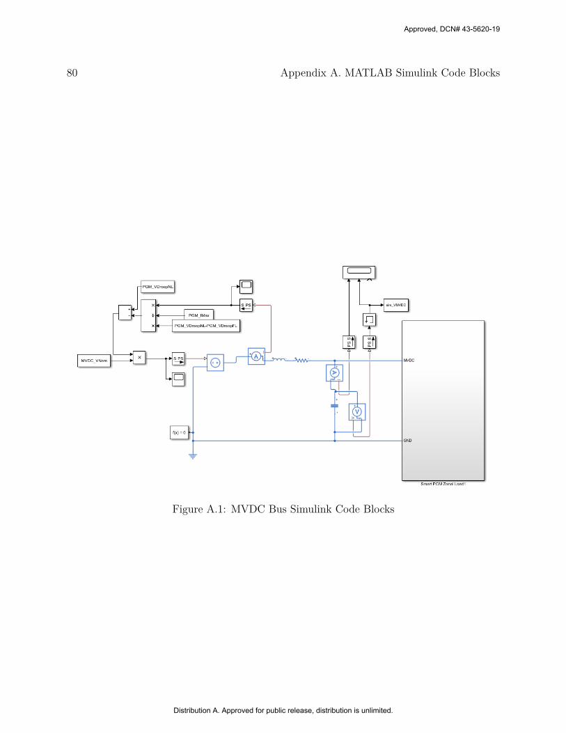
80 Appendix A. MATLAB Simulink Code Blocks
Figure A.1: MVDC Bus Simulink Code Blocks
Approved, DCN# 43-5620-19
Distribution A. Approved for public release, distribution is unlimited.

81
Figure A.2: Full PCM Simulink Code Blocks - Part A
Approved, DCN# 43-5620-19
Distribution A. Approved for public release, distribution is unlimited.

82 Appendix A. MATLAB Simulink Code Blocks
Figure A.3: Full PCM Simulink Code Blocks - Part B
Approved, DCN# 43-5620-19
Distribution A. Approved for public release, distribution is unlimited.

83
Figure A.4: Dynamically Tunable Virtual RC Stabilizer Simulink Code Blocks
Approved, DCN# 43-5620-19
Distribution A. Approved for public release, distribution is unlimited.