Embed Size (px)
Citation preview

Rev. 1.1 11/10 Copyright © 2010 by Silicon Laboratories Si3402
Si3402
FULLY- INTEGRATED 802.3-COMPLIANT POE PD INTERFACE
AND LOW-EMI SWITCHING REGULATOR
Features
Applications
Description
The Si3402 integrates all power management and control functions requiredin a Power-over-Ethernet (PoE) powered device (PD) application. TheSi3402 converts the high voltage supplied over the 10/100/1000BASE-TEthernet connection into a regulated, low-voltage output supply. Theoptimized architecture of the Si3402 minimizes the solution footprint,reduces external BOM cost, and enables the use of low-cost externalcomponents while maintaining high performance. The Si3402 integrates therequired diode bridges and transient surge suppressor, thus enabling directconnection of the IC to the Ethernet RJ-45 connector. The switching powerFET and all associated functions are also integrated. The integratedswitching regulator supports isolated (flyback) and non-isolated (buck)converter topologies. The Si3402 supports IEEE Std 802.3™ 2008 (futureinstances are referred to as 802.3) compliant solutions as well as pre-standard products, all in a single IC. Standard external resistors connectedto the Si3402 provide the proper 802.3 signatures for the detection functionand programming of the classification mode. Startup circuits ensure well-controlled initial operation of both the hotswap switch and the voltageregulator. The Si3402 is available in a low-profile, 20-pin, 5 x 5 mm QFNpackage. While the Si3402 is designed for applications up to 10 W, it can beused for higher power applications (up to approximately 15 W). See also“AN313: Using the Si3401/2 in High Power Applications” for moreinformation.
IEEE 802.3 standard-compliant solution, including pre-standard (legacy) PoE support
Highly-integrated IC enables compact solution footprintsMinimal external componentsIntegrated diode bridges and
transient surge suppressorIntegrated switching regulator
controller with on-chip power FET
Integrated dual current-limited hotswap switch
Programmable classification circuit
Incorporates switcher EMI-reduction techniques.
Supports non-isolated and isolated switching topologies
Comprehensive protection circuitryTransient overvoltage
protectionUndervoltage lockoutEarly power-loss indicatorThermal shutdown protectionFoldback current limiting
Low-profile 5 x 5 mm 20-pin QFN RoHS-compliant
Voice over IP telephones and adapters
Wireless access points Security cameras
Point-of-sale terminals Internet appliances Network devices High power applications
Ordering Information:
See page 19.
Pin Assignments
5 x 5 mm QFN(Top View)
EROUT
SSFT
RD
ET
HS
O
RC
L
SP1
SP
2
VPOSF
CT1
PL
OS
SISOSSFT
VDD
5 6 7 8 9 10
151620 19 18 17
1
2
3
4 11
12
13
14
VN
EG
VS
SA
VP
OS
S
VS
S1
SW
O
VS
S2
FB
VNEG(PAD)
CT2

Si3402
2 Rev. 1.1
Functional Block Diagram
Detection&
Classification
HotswapSwitch
&Current limit
HotswapControl
&Common
Bias
PWM Control and EMI Limiting
SwitchingFET
Rec
tific
atio
n&
Prot
ectio
nCT1
CT2
SP1
SP2
VPOSF
VNEG
RDET RCL
HSO
VDD
PLOSS VSS1
SWO
EROUTFB
SSFT ISOSSFT
VSS2
VPOSS
VSSA

Si3402
Rev. 1.1 3
TABLE OF CONTENTS
Section Page
1. Electrical Specifications . . . . . . . . . . . . . . . . . . . . . . . . . . . . . . . . . . . . . . . . . . . . . . . . . . .42. Typical Application Schematics . . . . . . . . . . . . . . . . . . . . . . . . . . . . . . . . . . . . . . . . . . . . .93. Functional Description . . . . . . . . . . . . . . . . . . . . . . . . . . . . . . . . . . . . . . . . . . . . . . . . . . .11
3.1. Overview . . . . . . . . . . . . . . . . . . . . . . . . . . . . . . . . . . . . . . . . . . . . . . . . . . . . . . . . . .113.2. PD Hotswap Controller . . . . . . . . . . . . . . . . . . . . . . . . . . . . . . . . . . . . . . . . . . . . . . .113.3. Switching Regulator . . . . . . . . . . . . . . . . . . . . . . . . . . . . . . . . . . . . . . . . . . . . . . . . .14
4. Pin Descriptions . . . . . . . . . . . . . . . . . . . . . . . . . . . . . . . . . . . . . . . . . . . . . . . . . . . . . . . . .165. Package Outline . . . . . . . . . . . . . . . . . . . . . . . . . . . . . . . . . . . . . . . . . . . . . . . . . . . . . . . . .176. Recommended Land Pattern for the Si3402 . . . . . . . . . . . . . . . . . . . . . . . . . . . . . . . . . .187. Ordering Guide . . . . . . . . . . . . . . . . . . . . . . . . . . . . . . . . . . . . . . . . . . . . . . . . . . . . . . . . . .19Document Change List . . . . . . . . . . . . . . . . . . . . . . . . . . . . . . . . . . . . . . . . . . . . . . . . . . . . .20Contact Information . . . . . . . . . . . . . . . . . . . . . . . . . . . . . . . . . . . . . . . . . . . . . . . . . . . . . . . .22

Si3402
4 Rev. 1.1
1. Electrical Specifications
Table 1. Recommended Operating Conditions
Description Symbol Min Typ Max Units
|CT1 – CT2| or |SP1 – SP2| VPORT 2.8 — 57 V
Ambient Operating Temperature TA –40 25 85 °C
Note: Unless otherwise noted, all voltages referenced to VNEG. All minimum and maximum specifications are guaranteed and apply across the recommended operating conditions. Typical values apply at nominal supply voltage and ambient temperature unless otherwise noted.
Table 2. Absolute Maximum Ratings (DC)1
Type Description Rating Unit
Voltage
CT1 to CT2 –60 to 60
V
SP1 to SP2 –60 to 60
VPOS2 –0.3 to 60
HSO –0.3 to 60
VSS1, VSS2, or VSSA –0.3 to 60
SWO –0.3 to 60
PLOSS to VPOS2 –60 to 0.3
RDET –0.3 to 60
RCL –0.3 to 5
SSFT to VPOS2 –5 to 0.3
ISOSSFT to VSS1, VSS2, or VSSA –0.3 to VDD+0.3
FB to VPOS –5 to 0.3
EROUT to VSS1, VSS2, or VSSA –0.3 to VDD+0.3
VSS1 to VSS2 or VSSA –0.3 to 0.3
VDD to VSS1, VSS2, or VSSA –0.3 to 5
Notes:1. Unless otherwise noted, all voltages referenced to VNEG. Permanent device damage may occur if the maximum
ratings are exceeded. Functional operation should be restricted to those conditions specified in the operational sections of this data sheet. Exposure to absolute maximum rating conditions for extended periods may adversely affect device reliability.
2. VPOS is equal to VPOSF and VPOSS tied together for test condition purposes.

Si3402
Rev. 1.1 5
Current
RCL 0 to 100
mA
RDET 0 to 1
CT1, CT2, SP1, SP2 –400 to 400
VPOS2 –400 to 400
HSO 0 to 400
PLOSS –0.5 to 5
VDD 0 to 2
SWO 0 to 400
VSS1, VSS2, or VSSA –400 to 0
AmbientTemperature
Storage –65 to 150°C
Operating –40 to 85
Table 2. Absolute Maximum Ratings (DC)1 (Continued)
Type Description Rating Unit
Notes:1. Unless otherwise noted, all voltages referenced to VNEG. Permanent device damage may occur if the maximum
ratings are exceeded. Functional operation should be restricted to those conditions specified in the operational sections of this data sheet. Exposure to absolute maximum rating conditions for extended periods may adversely affect device reliability.
2. VPOS is equal to VPOSF and VPOSS tied together for test condition purposes.
Si3402
6 Rev. 1.1
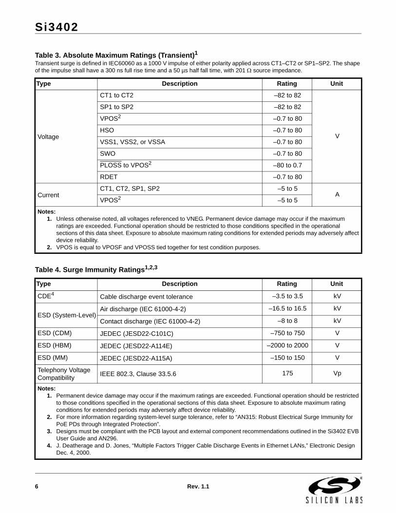
Table 3. Absolute Maximum Ratings (Transient)1
Transient surge is defined in IEC60060 as a 1000 V impulse of either polarity applied across CT1–CT2 or SP1–SP2. The shape of the impulse shall have a 300 ns full rise time and a 50 µs half fall time, with 201 source impedance.
Type Description Rating Unit
Voltage
CT1 to CT2 –82 to 82
V
SP1 to SP2 –82 to 82
VPOS2 –0.7 to 80
HSO –0.7 to 80
VSS1, VSS2, or VSSA –0.7 to 80
SWO –0.7 to 80
PLOSS to VPOS2 –80 to 0.7
RDET –0.7 to 80
CurrentCT1, CT2, SP1, SP2 –5 to 5
AVPOS2 –5 to 5
Notes:1. Unless otherwise noted, all voltages referenced to VNEG. Permanent device damage may occur if the maximum
ratings are exceeded. Functional operation should be restricted to those conditions specified in the operational sections of this data sheet. Exposure to absolute maximum rating conditions for extended periods may adversely affect device reliability.
2. VPOS is equal to VPOSF and VPOSS tied together for test condition purposes.
Table 4. Surge Immunity Ratings1,2,3
Type Description Rating Unit
CDE4 Cable discharge event tolerance –3.5 to 3.5 kV
ESD (System-Level)Air discharge (IEC 61000-4-2) –16.5 to 16.5 kV
Contact discharge (IEC 61000-4-2) –8 to 8 kV
ESD (CDM) JEDEC (JESD22-C101C) –750 to 750 V
ESD (HBM) JEDEC (JESD22-A114E) –2000 to 2000 V
ESD (MM) JEDEC (JESD22-A115A) –150 to 150 V
Telephony Voltage Compatibility
IEEE 802.3, Clause 33.5.6 175 Vp
Notes:1. Permanent device damage may occur if the maximum ratings are exceeded. Functional operation should be restricted
to those conditions specified in the operational sections of this data sheet. Exposure to absolute maximum rating conditions for extended periods may adversely affect device reliability.
2. For more information regarding system-level surge tolerance, refer to “AN315: Robust Electrical Surge Immunity for PoE PDs through Integrated Protection”.
3. Designs must be compliant with the PCB layout and external component recommendations outlined in the Si3402 EVB User Guide and AN296.
4. J. Deatherage and D. Jones, “Multiple Factors Trigger Cable Discharge Events in Ethernet LANs,” Electronic Design Dec. 4, 2000.

Si3402
Rev. 1.1 7
Table 5. Electrical Characteristics
Parameter Description Min Typ Max Unit
VPORT
Detection 2.7 — 11
V
Classification 14 — 22
UVLO Turn Off — — 42
UVLO Turn On 30 — 36
Transient Surge1 62 — 79
Input Offset Current VPORT < 10 V — — 10 µA
Diode Bridge Leakage VPORT = 57 V — — 25 µA
IPORT Classification2
Class 0 0 — 4
mA
Class 1 9 — 12
Class 2 17 — 20
Class 3 26 — 30
Class 4 36 — 44
IPORT Operating Current3 36 V < VPORT < 57 V — 2 3.1 mA
Current Limit4Inrush — 140 — mA
Operating 470 — 680 mA
Hotswap FET On-Resistance + RSENSE
36 V < VPORT < 57 V 0.5 — 1.5
Power Loss VPORT Threshold 27 30 33 V
Switcher Frequency — 350 — kHz
Maximum Switcher Duty Cycle5 ISOSSFT connected to VDD
— 50 —%
Switching FET On-Resistance 0.3 — 0.86
Regulated Feedback @ Pin FB6 DC Avg. — 1.23 — V
Regulated Output Voltage Tolerance6 Output voltage tolerance @ VOUT
–5 — 5%
Notes:1. Transient surge defined in IEC60060 as a 1000 V impulse of either polarity applied to CT1–CT2 or SP1–SP2. The
shape of the impulse shall have a 300 ns full rise time and a 50 µs half fall time with 201 source impedance.2. The classification currents are guaranteed only when recommended RCLASS resistors are used, as specified in
Table 11.3. IPORT includes full operating current of switching regulator controller.4. The PD interface includes dual-level input current limit. At turn-on, before the HSO load capacitor is charged, the
current limit is set at the inrush level. After the capacitor has been charged within ~1.25 V of VNEG, the operating current limit is engaged. This higher current limit remains active until the UVLO lower limit has been tripped or until the hotswap switch is sufficiently current-limited to cause a foldback of the HSO voltage.
5. See “AN296: Using the Si3400/1/2 PoE PD Controller in Isolated and Non-Isolated Designs” for more information.6. Applies to non-isolated applications only (VOUT on schematic in Figure 1).

Si3402
8 Rev. 1.1
VDD Accuracy @ 0.8 mA 36 V < VPORT < 57 V 4.5 — 5.5 V
Softstart Charging CurrentSSFT pin — 25 — µA
ISOSSFT pin — 13 — µA
Thermal Shutdown Junction temperature — 160 — ºC
Thermal Shutdown Hysteresis — — 25 ºC
Table 6. Total Power Dissipation
Description Condition Min Typ Max Units
Power Dissipation VPORT = 50 V, VOUT = 5 V, 2 A — 1.2 — W
Power Dissipation*VPORT = 50 V, VOUT = 5 V, 2 A w/ diode bridges bypassed
— 0.7 — W
*Note: Silicon Laboratories recommends the on-chip diode bridges be bypassed when output power requirements are >10 W or in thermally-constrained applications. For more information, see “AN313: Using the Si3401/2 in High Power Applications”.
Table 7. Package Thermal Characteristics
Parameter Symbol Test Condition Typ Units
Thermal Resistance(Junction to Ambient)
JA
Still air; assumes a minimum of nine thermal vias are connected to a 2 in2 heat spreader plane for the package “pad” node (VNEG).
44 °C/W
Table 5. Electrical Characteristics (Continued)
Parameter Description Min Typ Max Unit
Notes:1. Transient surge defined in IEC60060 as a 1000 V impulse of either polarity applied to CT1–CT2 or SP1–SP2. The
shape of the impulse shall have a 300 ns full rise time and a 50 µs half fall time with 201 source impedance.2. The classification currents are guaranteed only when recommended RCLASS resistors are used, as specified in
Table 11.3. IPORT includes full operating current of switching regulator controller.4. The PD interface includes dual-level input current limit. At turn-on, before the HSO load capacitor is charged, the
current limit is set at the inrush level. After the capacitor has been charged within ~1.25 V of VNEG, the operating current limit is engaged. This higher current limit remains active until the UVLO lower limit has been tripped or until the hotswap switch is sufficiently current-limited to cause a foldback of the HSO voltage.
5. See “AN296: Using the Si3400/1/2 PoE PD Controller in Isolated and Non-Isolated Designs” for more information.6. Applies to non-isolated applications only (VOUT on schematic in Figure 1).

Si3402
Rev. 1.1 9
2. Typical Application Schematics
Figure 1. Schematic—Class 0 with Non-Isolated 5 V Output*
*Note: This is a simplified schematic. See “AN296: Using the Si3400/1/2 PoE PD Controller in Isolated and Non-Isolated Designs” for more details and complete application schematics.
Table 8. Component Listing—Class 0 with 5 V Output
Item Type Value Toler. Rating Notes
C1 Capacitor 15 µF 20% 100 V Switcher supply capacitor. Several paral-lel capacitors are used for lower ESR.
C2 Capacitor 0.1 µF 20% 100 V PD input supply capacitor.
C3 Capacitor 1000 µF 20% 10 V Switcher load capacitor - 1000 µF in par-allel with and X5R 22 µF for lower ESR.
C4 Capacitor 0.1 µF 20% 16 V VDD bypass capacitor.
C5 Capacitor 0.1 µF 10% 16 V Softstart capacitor.
C6 Capacitor 3.3 nF 10% 16 V Compensation capacitor.
C7 Capacitor 150 pF 10% 16 V Compensation capacitor.
R1 Resistor 25.5 k 1% 1/16 W Detection resistor.
R2 Resistor 8.66 k 1% 1/16 W Feedback resistor divider.
R3 Resistor 2.87 k 1% 1/16 W Feedback resistor divider.
R4 Resistor 30.1 k 1% 1/16 W Feedback compensation resistor.
D1 Diode 100 V Schottky diode; part no. PDS5100.
L1 Inductor 33 µH 20% 3.5 A Coilcraft part no. DO5010333.
C1
Si3402
RJ-45
ToEthernet PHY
R1
VN
EGRCL
RDET
CT1
CT2
SP1
SP2V
PO
SF
HS
O
VS
S1
L1
SWO
D1R2
R3
FB
PL
OS
SS
SF
T
EROUT
Vout
VD
D
C2
C3
C5
ISO
SS
FT
VS
S2
VP
OS
SC6
R4
C4
VS
SA
C7
Si3402
10 Rev. 1.1
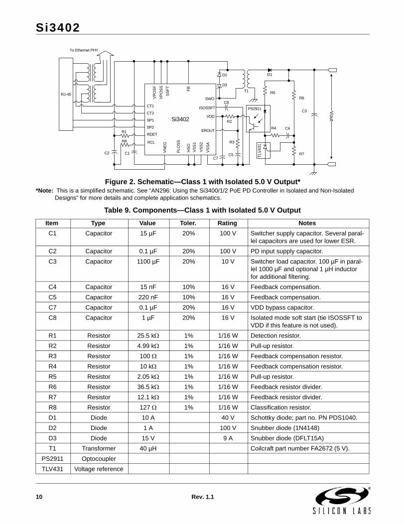
Figure 2. Schematic—Class 1 with Isolated 5.0 V Output**Note: This is a simplified schematic. See “AN296: Using the Si3400/1/2 PoE PD Controller in Isolated and Non-Isolated
Designs” for more details and complete application schematics.
Table 9. Components—Class 1 with Isolated 5.0 V Output
Item Type Value Toler. Rating Notes
C1 Capacitor 15 µF 20% 100 V Switcher supply capacitor. Several paral-lel capacitors are used for lower ESR.
C2 Capacitor 0.1 µF 20% 100 V PD input supply capacitor.
C3 Capacitor 1100 µF 20% 10 V Switcher load capacitor. 100 µF in paral-lel 1000 µF and optional 1 µH inductor for additional filtering.
C4 Capacitor 15 nF 10% 16 V Feedback compensation.
C5 Capacitor 220 nF 10% 16 V Feedback compensation.
C7 Capacitor 0.1 µF 20% 16 V VDD bypass capacitor.
C8 Capacitor 1 µF 20% 16 V Isolated mode soft start (tie ISOSSFT to VDD if this feature is not used).
R1 Resistor 25.5 k 1% 1/16 W Detection resistor.
R2 Resistor 4.99 k 1% 1/16 W Pull-up resistor.
R3 Resistor 100 1% 1/16 W Feedback compensation resistor.
R4 Resistor 10 k 1% 1/16 W Feedback compensation resistor.
R5 Resistor 2.05 k 1% 1/16 W Pull-up resistor.
R6 Resistor 36.5 k 1% 1/16 W Feedback resistor divider.
R7 Resistor 12.1 k 1% 1/16 W Feedback resistor divider.
R8 Resistor 127 1% 1/16 W Classification resistor.
D1 Diode 10 A 40 V Schottky diode; part no. PN PDS1040.
D2 Diode 1 A 100 V Snubber diode (1N4148)
D3 Diode 15 V 9 A Snubber diode (DFLT15A)
T1 Transformer 40 µH Coilcraft part number FA2672 (5 V).
PS2911 Optocoupler
TLV431 Voltage reference
C1
Si3402
RJ-45
To Ethernet PHY
VN
EGRCL
RDET
CT1
CT2
SP1
SP2
C2 HS
O
VS
S1
SWO
C3
SS
FT
PLO
SS
D1
R5
R7
R6
TLV
431
PS2911
T1
R2
FB
VDD
EROUT
Vo
ut
R1
ISOSSFT
VS
S2 R3
C5
C4R4
C7V
PO
SF
VP
OS
S
R8
VS
SA
D2
D3
C8
Si3402
Rev. 1.1 11
3. Functional Description
The Si3402 consists of two major functions: a hotswapcontroller/interface and a complete pulse-width-modulated switching regulator (controller and powerFET).
3.1. OverviewThe hotswap interface of the Si3402 provides thecomplete front end of an 802.3-compliant PD. TheSi3402 also includes two full diode bridges, a transientvoltage surge suppressor, detection circuit,classification current source, and dual-level hotswapcurrent limiting switch. This high level of integrationenables direct connection to the RJ-45 connector,simplifies system design, and provides significantadvantages for reliability and protection. The Si3402requires only four standard external components(detection resistor, optional classification resistor, loadcapacitor, and input capacitor) to create a fully 802.3-compliant interface. For more information aboutsupporting higher-power applications, see “AN313:Using the Si3401/2 in High Power Applications” and“AN314: Power Combining Circuit for PoE for up to18.5 W Output”.
The Si3402 integrates a complete pulse-widthmodulated switching regulator that includes thecontroller and power FET. The switching regulatorutilizes a constant frequency pulse-width modulatedcontroller optimized for all possible load conditions inPoE applications. The regulator integrates a low on-resistance (Ron) switching power MOSFET thatminimizes power dissipation, increases overall regulatorefficiency, and simplifies system design. An integratederror amplifier, precision reference, and programmablesoft-start current source provide the flexibility of using anon-isolated buck regulator topology or an isolatedflyback regulator topology.
The Si3402 is designed to operate with both 802.3-compliant Power Sourcing Equipment (PSE) and pre-standard (legacy) PSEs that do not adhere to the 802.3specified inrush current limits. The Si3402 is compatiblewith compliant and legacy PSEs because it uses twolevels for the hotswap current limits. By setting the initialinrush current limit to a low level, a PD based on theSi3402 minimizes the current drawn from either acompliant or legacy PSE during startup. After poweringup, the Si3402 automatically switches to a higher-levelcurrent limit, thereby allowing the PD to consume up to12.95 W (the max power allowed by the 802.3specification).
The inrush current limit specified by the 802.3 standardcan generate high transient power dissipation in the PD.By properly sizing the devices and implementing on-chip thermal protection, the Si3402 can go throughmultiple turn-on sequences without overheating thepackage or damaging the device. The switchingregulator power MOSFET has been conservativelydesigned and sized to withstand the high peak currentscreated when converting a high-voltage, low-currentsupply into a low-voltage, high-current supply.Excessive power cycling or short circuit faults willengage the thermal overload protection to prevent theonboard power MOSFETs from exceeding their safeand reliable operating ranges.
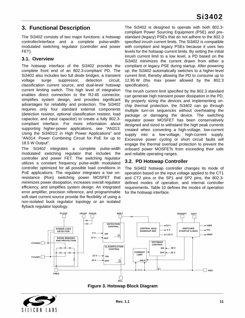
3.2. PD Hotswap ControllerThe Si3402 hotswap controller changes its mode ofoperation based on the input voltage applied to the CT1and CT2 pins or the SP1 and SP2 pins, the 802.3-defined modes of operation, and internal controllerrequirements. Table 10 defines the modes of operationfor the hotswap interface.
Figure 3. Hotswap Block Diagram
DIODE BRIDGESAND PROTECTION
DETECTIONCONTROL
ON
OFF
VPOSF
VNEG
CT1/SP1
CT2/SP2
0 V
12 V
RDET
CLASSIFICATIONCONTROL
ON
OFF
12 V
22 V
RCL
CENTRAL BIASBANDGAP REF
10 V
5 V
1.23 V
CURRENTLIMIT
HI/LO
HOTSWAPCONTROL
ON
OFF
39 V
32 V
SWITCHER STARTUP & BIAS
IABS
ITC
VREF
HSO
POWER LOSS DETECTOR
PLOSS SSFTVPOSS ISOSSFT

Si3402
12 Rev. 1.1
3.2.1. Rectification Diode Bridges and Surge Suppressor
The 802.3 specification defines the input voltage at theRJ-45 connector of the PD with no reference to polarity.In other words, the PD must be able to accept power ofeither polarity at each of its inputs. This requirementnecessitates the use of two sets of diode bridges, onefor the CT1 and CT2 pins and one for the SP1 and SP2pins to rectify the voltage. Furthermore, the standardrequires that a PD withstand a high-voltage transientsurge consisting of a 1000 V common-mode impulsewith 300 ns rise time and 50 µs half fall time. Typically,the diode bridge and the surge suppressor have beenimplemented externally, adding cost and complexity tothe PD system design.The diode bridge* and the surge suppressor have beenintegrated into the Si3402, thus reducing system costand design complexity.*Note: Silicon Laboratories recommends that on-chip diode
bridges be bypassed when >10 W of output power is required.
By integrating the diode bridges, the Si3402 gainsaccess to the input side of the diode bridge. Monitoringthe voltage at the input of the diode bridges instead ofthe voltage across the load capacitor provides theearliest indication of a power loss. This true early powerloss indicator, PLOSS, provides a local microcontrollertime to save states and shut down gracefully before theload capacitor discharges below the minimum 802.3-specified operating voltage of 36 V. Integration of thesurge suppressor enables optimization of the clampingvoltage and guarantees protection of all connectedcircuitry.
As an added benefit, the transient surge suppressor,when tripped, actively disables the hotswap interfaceand switching regulator, preventing downstream circuitsfrom encountering the high-energy transients.
3.2.2. Detection
In order to identify a device as a valid PD, a PSE willapply a voltage in the range of 2.8 to 10 V on the cableand look for the 25.5 k signature resistor. The Si3402will react to voltages in this range by connecting anexternal 25.5 k resistor between VPOS and VNEG.This external resistor and internal low-leakage controlcircuitry create the proper signature to alert the PSEthat a valid PD has been detected and is ready to havepower applied. The internal hotswap switch is disabledduring this time to prevent the switching regulator andattached load circuitry from generating errors in thedetection signature.
Since the Si3402 integrates the diode bridges, the ICcan compensate for the voltage and resistance effectsof the diode bridges. The 802.3 specification requiresthat the PSE use a multi-point, V/I measurementtechnique to remove the diode-induced dc offset fromthe signature resistance measurement. However, thespecification does not address the diode's nonlinearresistance and the error induced in the signatureresistor measurement. Since the diode's resistanceappears in series with the signature resistor, the PDsystem must find some way of compensating for thiserror. In systems where the diode bridges are external,compensation is difficult and suffers from errors. Sincethe diode bridges are integrated in the Si3402, the ICcan compensate for this error by offsetting resistanceacross all operating conditions and thus meeting the802.3 requirements. An added benefit is that thisfunction can be tested during the IC’s automated testingstep, guaranteeing system compliance when used inthe final PD application. For more information aboutsupporting higher-power applications (above 12.95 W),see “AN313: Using the Si3401/2 in High PowerApplications” and “AN314: Power Combining Circuit forPoE for up to 18.5 W Output”.
3.2.3. Classification
Once the PSE has detected a valid PD, the PSE mayclassify the PD for one of five power levels or classes. Aclass is based on the expected power consumption ofthe powered device. An external resistor sets thenominal class current that can then be read by the PSEto determine the proper power requirements of the PD.
When the PSE presents a fixed voltage between 15.5 Vand 20.5 V to the PD, the Si3402 asserts the classcurrent from VPOS through the RCL resistor. Theresistor values associated with each class are shown inTable 11.
Table 10. Hotswap Interface Modes
Input Voltage (|CT1-CT2| or |SP1-SP2|)
Si3402 Mode
0 to 2.7 V Inactive
2.7 to 11 V Detection signature
11 to 14 V Detection turns off and internal bias starts
14 to 22 V Classification signature
22 to 42 V Transition region
42 up to 57 V Switcher operating mode (hysteresis limit based on rising input voltage)
57 down to 36 V Switcher operating mode (hysteresis limit based on falling input voltage)
Si3402
Rev. 1.1 13
The 802.3 specification limits the classification time to75 ms to limit the power dissipated in the PD. If the PSEclassification period exceeds 75 ms and the dietemperature rises above the thermal shutdown limits,the thermal protection circuit will engage and disablethe classification current source in order to protect theSi3402. The Si3402 stays in classification mode untilthe input voltage exceeds 22 V (the upper end of itsclassification operation region).
3.2.4. Under Voltage Lockout
The 802.3 standard specifies the PD to turn on whenthe line voltage rises to 42 V and for the PD to turn offwhen the line voltage falls to 30 V. The PD must alsomaintain a large on-off hysteresis region to preventwiring losses between the PSE and the PD fromcausing startup oscillation.
The Si3402 incorporates an undervoltage lockout(UVLO) circuit to monitor the line voltage and determinewhen to apply power to the integrated switchingregulator. Before the power is applied to the switchingregulator, the hotswap switch output (HSO) pin is high-impedance and typically follows VPOS as the input isramped (due to the discharged switcher supplycapacitor). When the input voltage rises above theUVLO turn-on threshold, the Si3402 begins to turn onthe internal hotswap power MOSFET. The switchersupply capacitor begins to charge up under the currentlimit control of the Si3402, and the HSO pin transitionsfrom VPOS to VNEG. The Si3402 includes hystereticUVLO circuits to maintain power to the load until theinput voltage falls below the UVLO turn-off threshold.Once the input voltage falls below 30 V, the internalhotswap MOSFET is turned off.
3.2.5. Dual Current Limit and Switcher Turn-On
The Si3402 implements dual current limits. While thehotswap MOSFET is charging the switcher supplycapacitor, the Si3402 maintains a low current limit. Theswitching regulator is disabled until the voltage acrossthe hotswap MOSFET becomes sufficiently low,indicating the switcher supply capacitor is almostcompletely charged. When this threshold is reached,the switcher is activated, and the hotswap current limitis increased. This threshold also has hysteresis toprevent systemic oscillation as the switcher begins todraw current and the current limit is increased, whichallows resistive losses in the cable to effectivelydecrease the input supply.
The Si3402 stays in a high-level current limit mode untilthe input voltage drops below the UVLO turn-offthreshold or excessive power is dissipated in thehotswap switch. This dual level current limit allows thesystem designer to design powered devices for use withboth legacy and compliant PoE systems.
An additional feature of the dual current limit circuitry isfoldback current limiting in the event of a fault condition.When the current limit is switched to the higher level,400 mA of current can be drawn by the PD. Should afault cause more than this current to be consumed, thevoltage across the hotswap MOSFET will increase toclamp the maximum amount of power consumed. Thepower dissipated by the MOSFET can be very highunder this condition. If the fault is very low impedance,the voltage across the hotswap MOSFET will continueto rise until the lower current limit level is engaged,further reducing the dissipated power. If the faultcondition remains, the thermal overload protectioncircuitry will eventually engage and shut down thehotswap interface and switching regulator. The foldbackcurrent limiting occurs much faster than the thermaloverload protection and is, therefore, necessary forcomprehensive protection of the hotswap MOSFET.
Table 11. Class Resistor Values
Class Usage Peak Power Levels Nominal Class Current
RCL Resistor (1%,1/16 W)
0 Default 0.44 to 12.95 W < 4 mA > 1.33 k(or open circuit)
1 Optional 0.44 to 3.84 W 10.5 mA 127
2 Optional 3.84 to 6.49 W 18.5 mA 69.8
3 Optional 6.49 to 12.95 W 28 mA 45.3
4 PoE+ 12.95 to 17 W 40 mA 30.9

Si3402
14 Rev. 1.1
3.2.6. Power Loss Indicator
A situation can occur in which power is lost at the inputof the diode bridge and the hotswap controller does notdetect the fault due to the VPOS to VNEG capacitormaintaining the voltage. In such a situation, the PD canremain operational for hundreds of microsecondsdespite the PSE having removed the line voltage. If it isrecognized early enough, the time from power loss topower failure can provide valuable time to gracefullyshut down an application.
Due to integration of the diode bridges, the Si3402 isable to instantaneously detect the removal of the linevoltage and provide that early warning signal to the PDapplication. The PLOSS pin is an open drain output thatpulls up to VPOS when a line voltage greater than 27 Vis applied. When the line voltage falls below 27 V, theoutput becomes high-impedance, allowing an externalpull-down resistor to change the logic state of PLOSS.The benefit of this indicator is that the powered devicemay include a microcontroller that can quickly save itsmemory or operational state before draining the supplycapacitors and powering itself down. This feature canhelp improve overall manageability in applications, suchas wireless access points.
3.3. Switching RegulatorPower over Ethernet (PoE) applications fall into twobroad categories, isolated and non-isolated. Non-isolated systems can be used when the powered deviceis self-contained and does not provide externalconductors to the user or another application. Non-isolated applications include wireless access points and
security cameras. In these applications, there is noexplicit need for dc isolation between the switchingregulator output and the hotswap interface. An isolatedsystem must be used when the powered deviceinterfaces with other self-powered equipment or hasexternal conductors accessible to the user or otherapplications. For proper operation, the regulated outputsupply of the switching regulator must not have a dcelectrical path to the hotswap interface or switchingregulator primary side. Isolated applications includepoint-of-sale terminals where the user can touch thegrounded metal chassis.
The application determines the converter topology. Anisolated application will require a flyback transformer-based switching topology while a non-isolatedapplication can use an inductor-based buck convertertopology. In the isolated case, dc isolation is achievedthrough a transformer in the forward path and a voltagereference plus opto-isolator in the feedback path. Theapplication circuit shown in Figure 2 is an example ofsuch a topology. The non-isolated application inFigure 1 makes use of a single inductor as the energyconversion element, and the feedback signal is directlysupplied into the internal error amplifier. As can be seenfrom the application circuits, the isolated topology hasan increased number of components, thus increasingthe bill of materials (BOM) and system footprint.
To optimize cost and ease implementation, eachapplication should be evaluated for its isolated or non-isolated requirements.
Figure 4. Switcher Block Diagram
VSS1
SWITCHDRIVE
SWITCHER STARTUP & BIAS
IABS
ITC
VREF
PULSE-WIDTH
MODULATOR
OSCILLATOR
ERRORAMPLIFIER
EROUTFBSSFT
VDD
SWO
VPOSS
HSO VSS2
VPOSF
VSSAISOSSFT

Si3402
Rev. 1.1 15
3.3.1. Switcher Startup
The switching regulator is disabled until the hotswapinterface has both identified itself to the PSE andcharged the supply capacitor needed to filter theswitching regulator's high-current transients. Once thesupply capacitor is charged, the hotswap controllerengages the internal bias currents and supplies used bythe switcher. Additionally, the soft-start current begins tocharge the external soft-start capacitor.
The voltage developed across the soft-start capacitorserves as the error amplifier's reference in the non-isolated application. Ramping this voltage slowly allowsthe switching regulator to bring up the regulated outputvoltage in a controlled manner. Controlling the initialstartup of the regulated voltage restrains powerdissipation in the switching FET and prevents overshootand ringing in the output supply voltage.
In the isolated mode, a capacitor connected betweenpins ISOSSFT and VSSA slowly ramps the duty cycleclamp in the PWM circuit. Tie this pin to VDD if it is notused.
3.3.2. Switching Regulator Operation
The switching regulator of the Si3402 is constant-frequency, pulse-width-modulated (PWM), andcontroller integrated with switching power FETsoptimized for the output power range defined by the802.3 specification.
Once the hotswap interface has ensured proper turn-onof the switching regulator controller, the switcher is fullyoperational. An internal free-running oscillator andinternal precision voltage reference are fed into thepulse-width modulator. The output of the error amplifier(either internal for non-isolated applications or externalfor isolated applications) is also routed into the PWMand determines the slicing of the oscillator.
The PWM controls the switching FET drive circuitry. Asignificant advantage of integrating the switching powerFET onto the same monolithic IC as the switchingregulator controller is the ability to precisely adjust thedrive strength and timing to the FET's sizable gate,resulting in high regulator efficiency. Furthermore,current-limiting circuitry prevents the switching FETfrom sinking too much current, dissipating too muchpower, and becoming damaged. Thermal overloadprotection provides a secondary level of protection.
The flexibility of the Si3402's switching regulator allowsthe system designer to realize either the isolated or non-isolated application circuitry using a single device. Inoperation, the integration of the switching FET allowstighter control and more efficient operation than ageneral-purpose switching regulator coupled with ageneral-purpose external FET.
3.3.3. Flyback Snubber
Extremely high voltages can be generated by theinductive kick associated with the leakage inductance ofthe primary side of the flyback transformer used inisolated applications.
Refer to “AN296: Using the Si3400/1/2 PoE PDController in Isolated and Non-Isolated Designs” formore information on the snubber.

Si3402
16 Rev. 1.1
4. Pin Descriptions
Table 12. Si3402 Pin Descriptions (Top View)
Pin# Name Description
1 EROUT Error-amplifier output and PWM input; directly connected to opto-coupler in isolated application.
2 SSFT Soft-start output pin ramps voltage across external soft-start capacitor to allow switcher to ramp output slowly.
3 VDD 5 V supply rail for switcher; provides drive for opto-coupler.
4 ISOSSFT Isolated mode soft start enable input. Tie to VDD for non-isolated applications. Connect a 0.1 µF capacitor between this pin and VSSA for isolated applications.
5 PLOSS Early power loss indicator; open drain output is pulled to VPOS when VPORT is applied.
6 RDET Input pin for external precision detection resistor; also used for establishing absolute current reference.
7 HSO Hotswap switch output; connects to VNEG through hotswap switch.
8 RCL Input pin for external precision classification resistor; float if optional RCLASS is unused.
9, Pad VNEGRectified high-voltage supply, negative rail. Must be connected to thermal PAD node (VNEG) on package bottom. This thermal pad must be connected to VNEG (pin #9) as well as a 2 in2 heat spreader plane using a minimum of nine thermal vias.
10 SP2 High-voltage supply input from spare pair; polarity-insensitive.
11 SP1 High-voltage supply input from spare pair; polarity-insensitive.
12 VPOSF Rectified high-voltage supply, positive rail (force node)
13 CT2 High-voltage supply input from center tap of Ethernet transformer; polarity-insensitive.
14 CT1 High-voltage supply input from center tap of Ethernet transformer; polarity-insensitive.
15 VSSA Analog ground.
16 VPOSS Rectified high-voltage supply, positive rail sense node.
17 VSS1 Negative supply rail for switcher; externally tied to HSO.
18 SWO Switching transistor output; drain of switching N-FET.
19 VSS2 Negative supply rail for switcher; externally tied to HSO.
20 FB Regulated feedback input in non-isolated application.
EROUT
SSFT
RD
ET
HS
O
RC
L
SP1
SP
2
VPOSF
CT1
PL
OS
S
ISOSSFT
VDD
5 6 7 8 9 10
151620 19 18 17
1
2
3
4 11
12
13
14
VN
EG
VS
SA
VP
OS
S
VS
S1
SW
O
VS
S2
FB
VNEG(PAD)
CT2

Si3402
Rev. 1.1 17
5. Package Outline
Figure 5 illustrates the package details for the Si3402. Table 13 lists the values for the dimensions shown in theillustration.
Figure 5. 20-Lead Quad Flat No-Lead Package (QFN)
Table 13. Package Dimensions
Dimension Min Nom Max
A 0.80 0.85 0.90
A1 0.00 0.02 0.05
b 0.25 0.30 0.35
D 5.00 BSC.
D2 2.60 2.70 2.80
e 0.80 BSC.
E 5.00 BSC.
E2 2.60 2.70 2.80
L 0.50 0.55 0.60
L1 0.00 — 0.10
aaa — — 0.10
bbb — — 0.10
ccc — — 0.08
ddd — — 0.10
Notes:1. All dimensions shown are in millimeters (mm) unless otherwise noted.2. Dimensioning and tolerancing per ANSI Y14.5M-1994.3. This drawing conforms to the JEDEC Solid State Outline MO-220, Variation VHHB-1.

Si3402
18 Rev. 1.1
6. Recommended Land Pattern
Figure 6. Si3402 Recommended Land Pattern
Table 14. PCB Land Pattern Dimensions
Symbol Min Nom Max
P1 2.70 2.75 2.80
P2 2.70 2.75 2.80
X1 0.25 0.30 0.35
Y1 0.90 0.95 1.00
C1 4.70
C2 4.70
E 0.80
Notes:General
1. All dimensions shown are in millimeters (mm) unless otherwise noted.2. Dimensioning and Tolerancing is per the ANSI Y14.5M-1994 specification.3. This Land Pattern Design is based on the IPC-7351 guidelines.
Solder Mask Design
4. All metal pads are to be non-solder mask defined (NSMD). Clearance between the solder mask and the metal pad is to be 60 µm minimum, all the way around the pad.
Stencil Design
5. A stainless steel, laser-cut and electro-polished stencil with trapezoidal walls should be used to assure good solder paste release.
6. The stencil thickness should be 0.125 mm (5 mils).7. The ratio of stencil aperture to land pad size should be 1:1 for all perimeter pins.8. A 2x2 array of 1.2 mm square openings on 1.4 mm pitch should be used for the center ground pad.
Card Assembly
9. A No-Clean, Type-3 solder paste is recommended.10. The recommended card reflow profile is per the JEDEC/IPC J-STD-020 specification for Small Body
Components.

Si3402
Rev. 1.1 19
7. Ordering Guide
Part Number1,2 Package Temp Range Recommended
Maximum Output Power3
Si3402-A-GM 20-pin QFN,Pb-free; RoHS compliant
–40 to 85 °C < 10 W (IEEE 802.3 systems)17 W (proprietary high power)
Notes:1. “X” denotes product revision.2. Add an “R” at the end of the part number to denote tape and reel option.3. Refer to “AN313: Using the Si3401/2 in High Power Applications” and “AN314: Power Combining Circuit for PoE for up
to 18.5 W Output” for more information about using the Si3402 in higher power applications.

Si3402
20 Rev. 1.1
DOCUMENT CHANGE LIST
Revision 1.0 to Revision 1.1 Added "6. Recommended Land Pattern" on page 18.

Si3402
Rev. 1.1 21
NOTES:

Si3402
22 Rev. 1.1
CONTACT INFORMATIONSilicon Laboratories Inc.
400 West Cesar ChavezAustin, TX 78701Tel: 1+(512) 416-8500Fax: 1+(512) 416-9669Toll Free: 1+(877) 444-3032
Please visit the Silicon Labs Technical Support web page:https://www.silabs.com/support/pages/contacttechnicalsupport.aspxand register to submit a technical support request.
Silicon Laboratories and Silicon Labs are trademarks of Silicon Laboratories Inc.
Other products or brandnames mentioned herein are trademarks or registered trademarks of their respective holders.
The information in this document is believed to be accurate in all respects at the time of publication but is subject to change without notice. Silicon Laboratories assumes no responsibility for errors and omissions, and disclaims responsibility for any consequences resulting from the use of information included herein. Additionally, Silicon Laboratories assumes no responsibility for the functioning of undescribed features or parameters. Silicon Laboratories reserves the right to make changes without further notice. Silicon Laboratories makes no warranty, rep-resentation or guarantee regarding the suitability of its products for any particular purpose, nor does Silicon Laboratories assume any liability arising out of the application or use of any product or circuit, and specifically disclaims any and all liability, including without limitation conse-quential or incidental damages. Silicon Laboratories products are not designed, intended, or authorized for use in applications intended to support or sustain life, or for any other application in which the failure of the Silicon Laboratories product could create a situation where per-sonal injury or death may occur. Should Buyer purchase or use Silicon Laboratories products for any such unintended or unauthorized ap-plication, Buyer shall indemnify and hold Silicon Laboratories harmless against all claims and damages.