Embed Size (px)
Citation preview
Rev. 0.1 1/15 Copyright © 2015 by Silicon Laboratories AN732
AN732
Si4438 TX MATCHING
1. Introduction
This application note provides a description of the matching of the TX Power Amplifier (PA) on the Si4438 RFICworking in the 470–510 MHz Chinese AMR band. Specifically, this document does not address the matchingprocedure for the PA on the Si4460/4461 and Si4463 RFICs.
The matching network should simultaneously do the following:
Target a nominal output power level of +20 dBm (measured at connector to the antenna/load)
Obtain this nominal output power at a nominal supply voltage of VDD = 3.3 V
Minimize current consumption (i.e., maximize efficiency)
Constrain the peak voltage at the drain of the output devices
Comply with Chinese AMR specifications for spurious emissions
The matching procedures outlined in this document will allow for achieving the above-listed goals and areapplicable for three different types of board configurations: one with separate antennas for the TX and RX paths(Split TX/RX board configuration), one with a single antenna and the TX and RX paths tied directly together withoutuse of an RF switch (Direct Tie board configuration), and a third one where the TX and RX paths are connectedthrough a TX/RX switcher. The differences in the matching procedure required for the two board configurations arediscussed in detail.
Tables 1 and 2 are provided for users more interested in quickly obtaining matching component values than in themethodology used to develop the matching network. The power state, the current, and power data shown in thesetables are appropriate for a supply voltage of VDD = 3.3 V. At different VDD voltages tuning of the power state isrequired to keep the output power constant.
2. Overview of Matching Procedures
The PA circuitry in the Si4438 RFIC is not a conventional power amplifier (e.g., Class A/B/C) but instead is of a typeknown as a “switching power amplifier” or “switching power converter”. Use of a switching-type amplifier makes itpossible to obtain levels of efficiency not achievable with conventional amplifiers. However, the matchingprocedure for a switching PA is quite different and may not be immediately intuitive.
The recommended matching approach differs depending upon the desired frequency of operation. In the 470–510 MHz AMR band the recommended PA switching and operation type is the Class E. All reference designs (split,Dt and TX/RX switch) are detailed in this document.
2.1. Overview of Class-E Matching ProcedureThis application note discusses the Class-E matching procedure for the Si4438 RFIC in great detail. However,some readers may be interested in quickly gaining a high-level overview of the procedure before getting into thefine details. For those readers, the main points of the Class-E matching procedure are summarized below:
Choose LCHOKE (pull-up inductor) for high impedance at Fo
Choose C0 (series capacitor)
Use design equations to calculate L0 (series inductor) and CM (shunt capacitor)
Design a Chebyshev LPF (for attenuation of harmonics)

http://www.silabs.com
Silicon Laboratories Inc.400 West Cesar ChavezAustin, TX 78701USA
Smart. Connected. Energy-Friendly.
Productswww.silabs.com/products
Qualitywww.silabs.com/quality
Support and Communitycommunity.silabs.com
DisclaimerSilicon Laboratories intends to provide customers with the latest, accurate, and in-depth documentation of all peripherals and modules available for system and software implementers using or intending to use the Silicon Laboratories products. Characterization data, available modules and peripherals, memory sizes and memory addresses refer to each specific device, and "Typical" parameters provided can and do vary in different applications. Application examples described herein are for illustrative purposes only. Silicon Laboratories reserves the right to make changes without further notice and limitation to product information, specifications, and descriptions herein, and does not give warranties as to the accuracy or completeness of the included information. Silicon Laboratories shall have no liability for the consequences of use of the information supplied herein. This document does not imply or express copyright licenses granted hereunder to design or fabricate any integrated circuits. The products are not designed or authorized to be used within any Life Support System without the specific written consent of Silicon Laboratories. A "Life Support System" is any product or system intended to support or sustain life and/or health, which, if it fails, can be reasonably expected to result in significant personal injury or death. Silicon Laboratories products are not designed or authorized for military applications. Silicon Laboratories products shall under no circumstances be used in weapons of mass destruction including (but not limited to) nuclear, biological or chemical weapons, or missiles capable of delivering such weapons.
Trademark InformationSilicon Laboratories Inc.® , Silicon Laboratories®, Silicon Labs®, SiLabs® and the Silicon Labs logo®, Bluegiga®, Bluegiga Logo®, Clockbuilder®, CMEMS®, DSPLL®, EFM®, EFM32®, EFR, Ember®, Energy Micro, Energy Micro logo and combinations thereof, "the world’s most energy friendly microcontrollers", Ember®, EZLink®, EZRadio®, EZRadioPRO®, Gecko®, ISOmodem®, Precision32®, ProSLIC®, Simplicity Studio®, SiPHY®, Telegesis, the Telegesis Logo®, USBXpress® and others are trademarks or registered trademarks of Silicon Laborato-ries Inc. ARM, CORTEX, Cortex-M3 and THUMB are trademarks or registered trademarks of ARM Holdings. Keil is a registered trademark of ARM Limited. All other products or brand names mentioned herein are trademarks of their respective holders.

AN732
2 Rev. 0.1
2.2. Summary of Matching Network Component ValuesSome users are not greatly interested in the theoretical development of the matching network; rather, they areconcerned with quickly obtaining a set of component values for a given desired frequency of operation. For thoseusers, the resulting component values for the PA matching network for multiple frequencies across the operatingrange of the Si4438 RFIC are summarized in this section.
The matching networks may be realized with either wire-wound SMD inductors or with multi-layer SMD inductors.The cost of a multi-layer inductor is significantly lower than that of a wire-wound inductor, and thus in cost-sensitiveapplications the multi-layer solution is preferred. However, the performance of a circuit realization using only wire-wound inductors is generally better, due to the higher Qs and lower ohmic losses than multi-layer inductors ofequivalent value. The component values shown here are for a solution using wire-wound inductors such as the0402HP-series of wire-wound inductors from CoilCraft or the LQW15A or LQW18A series of wire-wound inductorsfrom Murata. Due to the increased loss, a realization using multi-layer inductors typically exhibits a slight increasein current consumption for the same amount of output power or, if the same power cannot be achieved, a slightlylower power with nearly the same current consumption. Surface-mount 0603-size or 0402-size componentsthemselves contain parasitic elements that modify their effective values at the frequency of interest. Furthermore, itis convenient to use the nearest available 5% or 10% component values rather than the exact component valuespredicted by Filter Design CAD software or filter prototype tables. Additionally, any printed circuit board layout hasparasitics, such as trace inductance, component pad capacitance, etc. This means that it will almost certainly benecessary to “tweak” the final matching values for the reader’s specific application and board layout. Thecomponent values given below should be used as starting points and the values modified slightly to zero-in on thebest filter response and impedance match to 50.
2.2.1. Component Values for Class-E Split TX/RX Board Configuration
Figure 1 shows the schematic with the component values with wire-wound inductors required for a Class-E matchusing the Split TX/RX board configuration. The element values of the match with multi-layer inductors are basicallythe same, if the inductance value exists. Unfortunately, for L0 and Lchoke this is not the case. In case of L0 andLchoke, nearby values are necessary to choose: the new L0 value is 22 nH while the new Lchoke value is 220 nHwith multi-layer inductors.
Table 1 shows the measured power and current and the used power setting both with wire-wound (WW) and multi-layer (ML) inductances at 3.3 V VDD. At other VDD levels the power setting needs to be tuned. Here the appliedmultilayer inductance type is the HQ series from Sunlord. Nearly the same or slightly lower power (0.3–0.4 dB) canbe achieved with Murata LQG15HS series inductors. In theory, the power can be raised back to +20 dBm withincreased power setting and current consumption, but longer-term reliability has not yet been tested with theseconditions.

AN732
Rev. 0.1 3
Figure 1. Class-E Matching Schematic for Split TX/RX Board Configuration
Table 1. Split TX/RX Board Power Setting, Power, Current Consumption and RX Sensitivity (40 Kbps, fdev=20KHz, 0.1% BER) both with Wire-Wound (WW) and Multi-Layer (ML) Inductors
Freq Band
DDAC [6:0] WW
Pout WW (dBm)
IDC WW (mA)
Sens WW (dBm)
DDAC[6:0] Pout ML (dBm)
IDC ML (mA) Sens ML (dBm)
470 MHz 46h 20.0 dBm 86.0 mA –109.3 dBm 46h 18.9 dBm 86.0 mA 109.1 dBm
490 MHz 46h 20.1 dBm 88.0 mA –109.4 dBm 46h 19.0 dBm 88.0 mA 109.2 dBm
510 MHz 46h 20.1 dBm 86.0 mA –109.3 dBm 46h 19.0 dBm 87.0 mA 109.2 dBm

AN732
4 Rev. 0.1
2.2.2. Component Values for Direct Tie Board Configuration
Figure 2 shows the schematic with the component values with wire-wound inductors required for a Class-E matchusing the Direct Tie board configuration. The element values of the match with multi-layer inductors are basicallythe same, if the value exists. Unfortunately, this is not the case for the L0 and Lchoke inductors. Here it isnecessary to choose nearby values: the proposed new L0 value is 22 nH while the Lchoke value is 220 nH withmulti-layer inductors.
Table 2 shows the measured power and current and the used power setting both with wire-wound (WW) and multi-layer (ML) inductances at 3.3 V VDD. At other VDD levels tuning of the power state is required. Here the appliedmulti-layer inductance type is the HQ series from Sunlord. Nearly the same or slightly lower power (0.3–0.4 dB)can be achieved with Murata LQG15HS series inductors. In theory, the power can be raised back to +20 dBm withincreased power setting and current consumption, but longer-term reliability has not yet been tested with theseconditions.
Figure 2. Class-E Matching Schematic for Direct Tie Board Configuration
AN732
Rev. 0.1 5
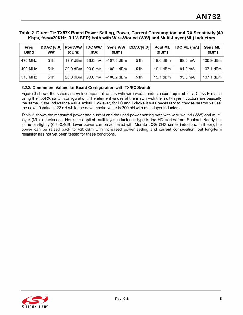
2.2.3. Component Values for Board Configuration with TX/RX Switch
Figure 3 shows the schematic with component values with wire-wound inductances required for a Class E matchusing the TX/RX switch configuration. The element values of the match with the multi-layer inductors are basicallythe same, if the inductance value exists. However, for L0 and Lchoke it was necessary to choose nearby values;the new L0 value is 22 nH while the new Lchoke value is 200 nH with multi-layer inductors.
Table 2 shows the measured power and current and the used power setting both with wire-wound (WW) and multi-layer (ML) inductances. Here the applied multi-layer inductance type is the HQ series from Sunlord. Nearly thesame or slightly (0.3–0.4dB) lower power can be achieved with Murata LQG15HS series inductors. In theory, thepower can be raised back to +20 dBm with increased power setting and current composition, but long-termreliability has not yet been tested for these conditions.
Table 2. Direct Tie TX/RX Board Power Setting, Power, Current Consumption and RX Sensitivity (40 Kbps, fdev=20KHz, 0.1% BER) both with Wire-Wound (WW) and Multi-Layer (ML) Inductors
Freq Band
DDAC [6:0] WW
Pout WW (dBm)
IDC WW (mA)
Sens WW (dBm)
DDAC[6:0] Pout ML (dBm)
IDC ML (mA) Sens ML (dBm)
470 MHz 51h 19.7 dBm 88.0 mA –107.8 dBm 51h 19.0 dBm 89.0 mA 106.9 dBm
490 MHz 51h 20.0 dBm 90.0 mA –108.1 dBm 51h 19.1 dBm 91.0 mA 107.1 dBm
510 MHz 51h 20.0 dBm 90.0 mA –108.2 dBm 51h 19.1 dBm 93.0 mA 107.1 dBm

AN732
6 Rev. 0.1
3. Power Amplifier Circuit Description
RF design engineers are familiar with matching conventional (Class A/B/C) power amplifiers. In such cases, thematching procedure is relatively simple: provide a load impedance that is the complex conjugate of the outputimpedance of the PA. The reader may also employ Load Pull techniques in which a match is found that optimizesthe output power but differs from the complex conjugate of the PA output impedance. In these conventional classesof power amplifiers, the output waveform ranges from a full 360 degree copy or reproduction of the drivingwaveform (e.g., Class A) to a partial (less than 360 degree) reproduction of the driving waveform (e.g., Class B orClass C).
As mentioned previously, the PA circuitry in the Si4438 RFIC differs considerably from such a conventional poweramplifier. The Si4438 RFIC uses a PA circuit of a type known as a “switching power amplifier” or “switching powerconverter”. The theory of operation of such amplifiers is discussed briefly in this document; for a deeper theoreticalunderstanding (including derivation of the design equations for Class-E amplifiers), the following papers arerecommended:
Class E – A New Class of High-Efficiency Tuned Single-Ended Switching Power Amplifiers, N. Sokal and A. Sokal, IEEE Journal of Solid State Circuits, Vol. SC-10, No. 3, June 1975.
Idealized Operation of the Class-E Tuned Power Amplifier, F. Raab, IEEE Transactions on Circuits and Systems, Vol. CAS-24, No. 12, December 1977.
3.1. Theory of Operation of an Ideal Switching PAAt the very heart of a switching PA is just that — a switch. In the Si4438, the switch is provided by an NMOScascode transistor in an open-drain configuration, sized to handle the current required for the specified outputpower.
Figure 3 shows the typical matching circuitry necessary to extract RF power from a switching amplifier whenmatched for Class-E operation. The value of the pull-up inductor LCHOKE is chosen to be a very large impedance atthe frequency of operation (and its nearest harmonics), while the series-resonant output tank (L0-C0) is chosen toresonate at the frequency of operation. The shunt capacitance CSHUNT is required to store energy during theswitching cycle. This shunt capacitance also works with matching components LX and CX to tailor the time-domainshape of the output waveform. It is important to understand that optimization of the efficiency of a switching-typeamplifier requires control of the time-domain shape of the output waveform.

AN732
Rev. 0.1 7
Figure 3. Basic Switching PA Circuit Topology
It may not be immediately clear to the reader how a switch “amplifies” an RF signal. From a purely technicalstandpoint, it does not. As long as the input control signal to the switch is sufficient in amplitude to toggle the switchbetween its ON and OFF states, the output waveform remains the same. The amount of output power delivered tothe load resistance is therefore independent of the amplitude of the input control signal (i.e., amplitude of the RFsignal at the gate of the output MOS device). In such a case, defining the “gain” or amplification factor of the PA nolonger has meaning. It is more accurate to refer to this circuit as a “power converter” rather than a “poweramplifier.”
In an ideal switching PA matched for Class-E operation, the level of output power is dependent primarily upon threeparameters: 1) the dc supply voltage, 2) the shunt output capacitance, and 3) the operating frequency. Therelationship between these parameters and the output power is shown in Equation 1. (The derivation for designequations is not provided within this document; please refer to the papers listed above for a deeper understandingof the operational theory.)
Equation 1.
This equation is interesting in that the output power is not a function of the load impedance. As will be shown later,it is necessary to present the correct value of load impedance to the device in order to obtain Class-E operation.However, once this load impedance is provided, the output power is adjusted either by increasing the supplyvoltage or by increasing the shunt capacitance CSHUNT at the output of the switching device.
POUT oCSHUNTVDD2
=

AN732
8 Rev. 0.1
Furthermore, it is theoretically possible to achieve 100% efficiency in an ideal switching PA. This is a significantdifference from conventional PAs. It is easily shown that the theoretical maximum efficiency of a Class-A PA is50%, 78.5% for Class-B, and so on. However, it is possible to tailor the output waveform in a switching PA suchthat the voltage across the switch is always zero during any period of time that the switch is conducting current,and the current conducted by the switch is always zero during any period of time that the voltage across the switchis non-zero. Thus the power dissipated by the switching device itself is zero, and the efficiency approaches 100%(in the absence of any other losses in the circuit). This is illustrated in a 315 MHz example in Figure 4, where it isobserved that non-zero values of the voltage and current waveforms never occur at the same time.
Figure 4. Theoretical Class-E Drain Voltage/Current Waveforms

AN732
Rev. 0.1 9
3.2. Limitations of a Practical MOS Switching PAThere is no theoretical limit to the amount of power that may be extracted from an ideal switching PA. In practice,several factors prevent achieving “ideal” operation. These factors include the maximum operating voltage of theswitch (i.e., MOS output device), the maximum current (limited by the size of the MOS output device), ON and OFFstate resistances of the MOS output device, non-zero switching times of the MOS output device, and losses in theoutput matching components due to finite Qs. All of these factors combine to limit the achievable output power andefficiency.
The limitation on the maximum drain voltage of the MOS output device turns out to be a considerable constraint.RF design engineers may be quite familiar with the waveforms obtained with inductively-loaded conventional PAs,where the peak output voltage reaches a value equal to twice the dc supply voltage. However, the peak of theoutput voltage waveform in a switching PA may far exceed this “2xVDD” rule-of-thumb. As is shown in the paperslisted above, the peak drain voltage for a Class-E switching amplifier can reach 3.56 x VDD.
The operational range of supply voltage for the Si4438 RFIC is specified as VDD = 1.8 V to 3.6 V. It is apparent thatif the switching PA circuit was matched for Class-E operation at VDD = 3.6 V, the resulting peak drain voltage wouldreach 12.8 V peak. This would appear to exceed the maximum voltage at which the MOS devices can operatewithout damage. However, there are several mechanisms which work to allow safe operation, even at themaximum specified VDD supply voltage. Internally, the PA has a cascode structure, and thus the total signal swingdoes not appear across one device but instead is divided across several devices. Additionally, the ON-stateresistance of the output devices is not zero; this resistance acts as a loss mechanism to further reduce the voltageswing across the internal device(s). As a result, Class-E matching and operation may be safely recommended forthe Si4438 RFIC.
The size of the MOS output device has the effect of limiting the amount of output power that can be extracted froma practical switching PA. In an ideal switching PA, the output power may be increased by either raising the supplyvoltage or by increasing the value of shunt output capacitance. As just discussed, an increase in supply voltageresults in an increase in peak drain voltage swing, and thus the supply voltage may not be raised indefinitely.Increasing the shunt output capacitance is therefore the only remaining option by which the output power may beincreased.
This has the effect of requiring greater current handling capability in the switching device. While an ideal switchmay carry an infinite amount of current, a practical MOS switch cannot. The size of the MOS output device in theSi4438 RFIC is carefully designed to carry sufficient current to achieve its maximum specified output power;however, this level of current-handling capability is only available when the RFIC is commanded to its maximum TXoutput power mode (by the DDAC[6:0] field in the PA_PWR_LVL property 0x2201). The Si4438 RFIC achieves areduction in output power by reducing the number of active fingers (i.e., size) of the MOS output device; thiseffectively limits the current-handling ability of the output device to less than that desired by the combination ofsupply voltage and output capacitance. That is to say, at the maximum setting(s) of the DDAC[6:0] field, the PAoutput devices behave much like a switch, but at the lower settings of the DDAC[6:0] field, the output devicesbehave more like a switch in series with a non-negligible resistance.
AN732
10 Rev. 0.1
4. Class-E Matching Procedure for the Si4438
As discussed above, the cascode design of the PA output devices in the Si4438 RFIC allows for Class-E operationwithout exceeding safe levels of peak drain voltage swing. Additionally, the Si4438 RFIC contains internal diodevoltage clamps on the drain node of the MOS output device. The purpose of these diode clamps is to limit briefexcursions of excess peak drain voltage. Such variations in peak drain voltage may occur if the antenna loadimpedance varies considerably from 50 Ω (e.g., turning on the TX output without an antenna connected, etc.).
This application note is largely targeted at applications which require +20 dBm output power. While this level ofoutput power is readily achievable, meeting all design constraints requires careful attention to matchingcomponent selection and good board layout techniques. It is possible to fall short of one or more design goalsthrough poor design and board layout practices.
4.1. Overview of Class-E Matching Procedure4.1.1. Split TX/RX Board Configuration
The following steps provide a broad overview of the matching methodology for Class-E operation on the Split TX/RX board configuration. Further details of each step will be provided later.
1. Choose LCHOKE (pull-up inductor) for high impedance at Fo (and its nearest harmonics).
2. Choose/calculate values for series-resonant tank L0-C0 such that L0-C0 resonates at Fo.
3. Calculate required value of ZLOAD, given the desired frequency of operation (Fo) and the shunt drain capacitance (CSHUNT = ~2.5 pF on the Si4438 RFIC around the 490 MHz band).
4. Calculate required value for the voltage-limiting resistor RDC, given the desired output power and VDD supply voltage. It has to be emphasized that in the tested circuits the external voltage limiting resistor is not used. Instead, the on-state FET resistance is tuned properly by setting the power state.
5. Calculate values for matching components LX and CM, given the antenna load resistance (e.g., RANT = 50 Ω) and the calculated value for ZLOAD.
6. Design a low-pass filter to provide sufficient attenuation of harmonic signals.
4.1.2. Direct Tie Board Configuration
The following steps provide a broad overview of the matching methodology for Class-E operation on the Split TX/RX board configuration. Further details of each step will be provided later.
1. Repeat Steps 1 through 6, as shown immediately above.
2. Construct a 4-element balun match to the differential RXp/RXn LNA input pins, using the methodology outlined in “AN643 Si446x RX LNA Matching”.
3. Connect the TX and RX paths together, and deliberately mis-tune L0 by increasing its value if required above its calculated optimum value.
4.2. Detailed Class-E Matching Procedure for Split TX/RX Board ConfigurationIn this section, further detail is provided about each step of the Class-E Split TX/RX matching procedure outlinedabove. A supply voltage of VDD = 3.3 V and an operation frequency of 470 MHz is assumed. The matching circuitsgiven in Section “2.2. Summary of Matching Network Component Values” are designed to 490 MHz centerfrequency.
4.2.1. Step #1: Select a Value for LCHOKE Pull-Up Inductor
In Step #1, an appropriate value is selected for the pull-up inductor LCHOKE.
In the theoretical derivation for Class-E switching amplifiers, the desired impedance of the pull-up inductor LCHOKEis zero at dc and infinite at all other frequencies. This is not achievable in practice; however, a large value ofinductance provides a reasonable approximation to this performance. The value of LCHOKE should be chosen suchthat it provides a high impedance at not only the fundamental operating frequency but also at the first few harmonicfrequencies as well. The inductance value should not be so large as to already be at (or past) parallel self-resonance at the desired operating frequency. The exact inductance value is not critical; however, Silicon

AN732
Rev. 0.1 11
Laboratories recommends the following range of inductance values (assuming 0402-size or 0603-size inductors)as a function of the desired operating frequency:
315 MHz: approximately 390 nH
470 MHz: approximately 220 nH
915 MHz: approximately 100 nH
4.2.2. Step #2: Choose/Calculate Values for L0-C0 Series-Resonant Tank
In Step #2, the L0-C0 tank is designed to be series-resonant at the desired operating frequency Fo.
It is self-evident that there are infinite combinations of L0-C0 values that can achieve resonance at a desiredfrequency. However, certain broad guidelines may be used to select one particular solution of component values.
First, the inductance and capacitance values should be neither extremely large or extremely small. Discreteinductors and capacitors with extremely large values are subject to degrading effects due to self-resonance.Discrete components with extremely small values are also subject to degrading effects due to componenttolerance. In either case, the actual resonant frequency of the tank may be significantly different than the frequencypredicted by mathematical calculations.
Second, in the theoretical derivation for Class-E switching amplifiers it is desired that the impedance of the L0-C0series-resonant tank be zero at Fo and infinite at all other frequencies. This is not achievable in practice; however,a reasonable approximation to this performance may be obtained by using values with a high L-to-C ratio.
Third, it is desirable to minimize the insertion loss of the resonant tank. As the quality factor (Q) of discreteinductors is generally much lower than that of discrete capacitors, it is important to select an L0-C0 ratio thatmaximizes the inductor Q. The Q of discrete inductors generally increases as the inductance value is alsoincreased, until the inductance approaches the value where self-resonance becomes a concern.
Finally, it is desirable to select component values that are near standard 5% tolerance values.
These considerations lead to the following guidelines for selecting the values for L0-C0:
The L0-C0 tank must resonate at Fo
The value of L0 should be chosen as large as possible,
While remaining low enough that effects of self-resonance are not an issue,
And are close to standard 5% tolerance values
Assuming a desired operating frequency of Fo = 470 MHz as an example, these guidelines lead to selection and/orcalculation of the following values for L0-C0:
C0 = 8.2 pF (chosen)
L0 = 13.903 nH (calculated)
4.2.3. Step #3: Calculate the Required Value for ZLOAD
In Step #3, the required value of load impedance is calculated. This represents the impedance that must bepresented to the output of the L0-C0 resonant tank, and is calculated at the fundamental operating frequency Fo.
In the theoretical derivation for Class-E switching amplifiers, it is shown that the required load impedance (ZLOAD)is a function of shunt drain capacitance (CSHUNT) and operating frequency (o = 2Fo) as follows:
Equation 2.
This equation states that the required load impedance (ZLOAD) does not vary with the desired level of output power,but depends only on the desired operating frequency and value of shunt drain capacitance. The value of internalshunt drain capacitance CSHUNT is a design parameter of the Si4438 RFIC and is not adjustable by the user. Thisshunt capacitance is composed primarily of the drain-source capacitance (Cds) of the output MOS devices. SiliconLaboratories states that the value of this internal shunt drain capacitance is approximately:
ZLOAD fund 0.2815
oCSHUNT----------------------------- e
j 49.0524=

AN732
12 Rev. 0.1
CSHUNT ~ 2.5 pF
Assuming a desired operating frequency of Fo = 470 MHz as an example, the following value for ZLOAD may becalculated:
Equation 3.
This value of load impedance (ZLOAD) is not the same parameter as the antenna impedance (ZANT), nor do theynecessarily have the same ohmic value. A matching network must be constructed that transforms the arbitraryvalue of antenna impedance ZANT into the required value of load impedance ZLOAD, as seen at the output of theL0-C0 resonant circuit.
4.2.4. Step # 4: Calculate the Required Value for Voltage-Limiting Resistor RDC
In Step #4, the value of the voltage-limiting resistor RDC required for the desired output power is calculated, given aspecified value of PA supply voltage (VDD_PA).
Equation 1 shows that for a given desired operating frequency, the only “knob” remaining to adjust the outputpower is the PA supply voltage VDD_PA, as the value of CSHUNT is an internal chip design parameter and is notadjustable by the user. This equation is solved for VDD_PA and found to be:
Equation 4.
Continuing the design example of 470 MHz and assuming a desired output power of +20 dBm (100 mW), therequired value of VDD_PA may be calculated:
Equation 5.
This equation states that if the voltage supplied to the top of pull-up inductor LCHOKE is equal to 2.076 V and thepreviously-calculated value of load impedance ZLOAD is presented to the chip, the resulting output power will bePOUT = 100 mW = +20 dBm.
This required PA supply voltage (VDD_PA) is significantly different than the general supply voltage (VDD) for the restof the RFIC. It is obviously not desirable to maintain two separate, independent sources of supply voltage for theRFIC; therefore, it is convenient to create the PA output supply voltage from the main supply voltage by means ofan I-R voltage drop across a resistor or a properly adjusted internal switcher loss.
As the theoretical efficiency of a Class-E switching amplifier is 100%, the average PA drain current IDD_PA may becalculated as:
Equation 6.
This equation may be solved for IDD_PA to obtain:
Equation 7.
ZLOAD 470M 0.2815
2 470M 2.5pF--------------------------------------------------- e
j 49.052424.87 j28.66+= =
VDD_PA
POUT
oCSHUNT---------------------------------=
VDD_PA0.1
22470M 2.5pF
----------------------------------------------------- 2.076V= =
POUT oCSHUNTVDD_PA2
IDD_PAVDD_PA= =
IDD_PA oCSHUNTVDD_PA=

AN732
Rev. 0.1 13
Given the main supply voltage for the remainder of the chip (VDD), and having previously calculated the requiredvalue of PA supply voltage (VDD_PA) and average PA drain current (IDD_PA), it is a simple matter to calculate therequired value for RDC:
Equation 8.
Continuing the design example of 470 MHz for +20 dBm output power, the following calculations are made:
Equation 9.
Assuming a general chip supply voltage of VDD = 3.3 V, the required value of RDC may be calculated as:
Equation 10.
Theoretically, this value of resistance must be placed in series with LCHOKE in order to drop the general chip supplyvoltage down to the value required to obtain the desired output power.
However, these calculations for the value of RDC assume theoretically-ideal Class-E operation. In practice, thecircuit will not behave exactly as predicted by these equations due to non-idealities such as non-zero ON-stateresistance, finite OFF-state resistance, non-zero switching times, and loss in the external matching components.As a result, the output power obtained for a given value of VDD supply voltage will almost certainly be slightly lessthan predicted by theory. Stated another way, it will almost always be necessary to use a smaller value of RDC thanpredicted by theory in order to obtain the desired value of output power. Some amount of post-calculation“tweaking” of the component values is considered a normal part of the PA matching process, especially if thetuning of the switcher’s ON-state resistance is used instead of an external RDC. In this case, a tweaking of thepower state is required at the applied supply voltage.
4.2.5. Step #5: Calculate the Values for Matching Components LX and CM
In Step #5, the values of the matching components (LX and CM) required to transform the given antennaimpedance (ZANT) into the required load impedance (ZLOAD) are calculated.
This matching effort may be accomplished by simple and normal design methods, such as use of a Smith Chart orimpedance matching CAD software (e.g., WinSmith™). Continuing the design example for 470 MHz and assumingan antenna impedance of ZANT = RANT = 50 Ω, it is found that a shunt capacitance CM = 6.81 pF and seriesinductance LX = 18.17 nH is required to transform RANT = 50 Ω to the required value of ZLOAD = 24.87 + j 28.66 Ω.The resulting circuit topology is shown in Figure 4.
This is only one possible solution for the required impedance transformation; other matching topologies could havebeen used as well. The reader should also note that the required LX-CM match topology depends upon the real partof the load impedance, Re(ZLOAD). In this example, the real part of the load impedance was less than 50 Ω andthus an appropriate matching topology consisted of a shunt capacitor (CM) and a series inductor (LX). In the eventthat Re(ZLOAD) had been greater than 50 Ω, an appropriate matching topology would have consisted of first aseries inductor (LX) followed by a shunt capacitor (CM).
It is apparent that series inductors L0 and LX may be combined into one equivalent inductor with a value equal tothe sum of their individual inductances, in order to reduce parts count. This is a normal and usual practice.
In the example shown here, the following component values (obtained through use of the above design equations)were obtained:
Fo = 470 MHz
RDC
VDD VDD_PA–
IDD_PA-------------------------------------=
IDD_PA 22470M 2.5pF 2.076V 48.16mA= =
RDC3.3 2.076–
0.04816----------------------------- 25.41= =

AN732
14 Rev. 0.1
POUT(TARGET) = +20 dBm
VDD = 3.3 V
CSHUNT = 2.5 pF
LCHOKE = 220 nH
RDC = 25.41 Ω
C0 = 6.81 pF
L0+LX = 32.15 nH
CM = 6.81 pF
In practice, these exact values would be rounded to the nearest available 5% tolerance parts (e.g., L0+LX = 30 nH,CM = 6.8 pF, RDC=24 ohms). Also, as mentioned previously, the external RDC resistor is not used in the Si4428matching. Instead the internal switcher on-state resistance is adjusted properly by the power setting (PDACregister value).
4.2.6. Step #6: Design a Lowpass Filter
In Step #6, a low-pass filter network is designed in order to attenuate the harmonics below the level required tomeet applicable regulatory standards (e.g., FCC or ETSI).
The signal at the output of the match shown in Figure 5 will likely contain relatively high levels of harmonics.Although the bandpass response of the series-resonant L0-C0 tank provides some attenuation of harmonic signals,it is generally not sufficient to meet applicable regulatory standards. This is normal for such a switching-amplifierand matching topology.
It is difficult for Silicon Laboratories to recommend one single low-pass filter design that is appropriate for allcustomers, as customers may operate under widely differing regulatory standards and harmonic requirements.Also, the radiation efficiency of the antenna selected by the customer is not known in advance. These factors makeit difficult for Silicon Laboratories to conclusively state the required filter attenuation characteristics. As areasonable compromise, the following design goals for the low-pass filter are chosen:
Minimal insertion loss at the desired operating frequency
Lowest filter order possible to achieve harmonic attenuation required to meet regulatory standard
1:1 impedance transformation (i.e. 50 input and 50 output impedance)
Note that the amplitude characteristics of the LPF in the lower portion of the passband are relatively unimportant.Because the output signal contains no frequency components below the fundamental frequency, the frequencyresponse of the filter below the desired operating frequency is of little consequence. It is therefore acceptable toselect the filter type (e.g., Butterworth, Chebyshev, Elliptic) based primarily upon the filter’s attenuationcharacteristics rather than its passband response.
A Butterworth filter design is sub-optimal because it provides relatively poor high-frequency attenuationcharacteristics; there is no need to sacrifice high-frequency attenuation in order to obtain a maximally-flat in-bandfrequency response.
Similarly, an Elliptic filter design (Cauer-Chebyshev) may provide insufficient attenuation at higher-order harmonicfrequencies. While it may be possible (and advantageous) to tune a transmission zero in the stopband to the exactfrequency of a problematic harmonic (e.g., N=2 or N=3), it is paid for with a decrease in attenuation at higherharmonic frequencies. Insufficient attenuation of higher-order harmonics may result.
As a result, a Chebyshev low-pass filter design is settled upon as an acceptable type of filter response.
With a Chebyshev filter, it is possible to obtain a greater rate of attenuation roll-off in the stopband by accepting alarger amount of amplitude ripple in the passband. However, this design trade-off should not be pushed too far. Bydesigning for a limited amount of passband amplitude ripple, an upper limit is placed on the filter insertion loss dueto mistuning of the component values and thus accidentally operating on a minimum of the amplitude rippleresponse rather than on a maximum. Silicon Laboratories recommends a Chebyshev passband amplitude ripple of 0.25 dB to 0.5 dB as providing a reasonable balance between high-frequency stopband attenuation and potential

AN732
Rev. 0.1 15
passband filter insertion loss due to component tolerance.
Figure 5. Ideal 3rd-Order 0.5 dB Chebyshev Filter Response at 470 MHz
Figure 5 shows the passband frequency response of an ideal (lossless) Chebyshev filter with 0.5 dB of amplituderipple in the passband. In order to minimize the insertion loss of the filter at the desired operating frequency, it isnecessary to design the cutoff frequency of the filter such that the desired operating frequency falls at one of thepassband amplitude ripple peaks (Cursor “A” in the plot). If the desired operating frequency fell on a minimum ofthe amplitude ripple response (rather than on a maximum), the filter insertion loss would increase and the TXoutput power would decrease.
Filter component values may be obtained by usual design methods, such as use of Filter Design CAD software ortables of normalized filter values scaled to the desired frequency of operation. Note that Silicon Laboratoriesrecommends designing the filter such that the desired operating frequency falls at a peak of the amplitude rippleresponse rather than at the 3 dB cutoff frequency or at the equal amplitude ripple cutoff frequency. In this manner,the insertion loss of the filter will be minimized, and the TX output power will be maximized. For a 3rd-order 0.1 dBChebyshev filter, the ratio of F3dB:FPEAK is approximately 1.60:1. That is, if the desired operating frequency is470 MHz, the filter must be designed for a 3 dB cutoff frequency of 470 x 1.60 = 752 MHz. For a 3rd-order 0.5 dB

AN732
16 Rev. 0.1
Chebyshev filter, the ratio of F3dB:FPEAK is approximately 1.346:1.
SPICE model simulations of non-ideal discrete components predict an in-band filter insertion loss of approximately1.0 dB at the desired operating frequency (470 MHz, in this example). While not desirable, this value of filterinsertion loss is fairly realistic, given the typical Qs of discrete components in 0402-size or 0603-size surface-mount packages. Discrete components of higher quality (e.g. wire-wound inductors) may be chosen in an effort toreduce insertion loss, but such parts are admittedly more expensive. The Si4438 RFIC is capable of providing thespecified output power (+20 dBm) at the antenna output connector (i.e., after the insertion loss of the match andlowpass filter).
4.3. Modification of Class-E Match for Direct Tie Board ConfigurationIn this section, further detail is provided about modifying the Class-E match for a Direct Tie board configuration. Asupply voltage of VDD = 3.3 V is assumed.
4.3.1. Concept of Direct Tie Matching
In the Direct Tie board configuration, the TX and RX paths are tied directly together at a common point without theuse of an RF switch. Careful design procedure must be followed to ensure that the RX input circuitry does not loaddown the TX output path while in TX mode, and that the TX output circuitry does not degrade receive performancewhile in RX mode.
The RX input circuitry of the Si4438 chip contains a set of switches that aids in isolation of the TX and RXfunctions. This set of switches is implemented internally as shown in Figure 6.
Figure 6. RX Input Switches for Direct Tie Operation

AN732
Rev. 0.1 17
These three switches are activated and closed simultaneously upon entering TX mode; the switches remain openin all other modes, including RX mode. Closing these switches during TX mode effectively shorts the RXp and RXninput pins together and also shorts them to GND. The effective circuit may be re-drawn as shown in Figure 7.Inductor LR2 and capacitor CR2 have effectively been placed in parallel by the closure of the switches, and areconnected to GND. If the values of these components are chosen for resonance at the desired operatingfrequency, a very high impedance is presented to the TX path resulting in very little degradation in TX outputpower. Also, by shorting the input pins of the LNA together and simultaneously to GND, the LNA is protected fromthe large signal swing of the TX signal. This feature allows connection of the TX path to the RX path withoutdamage to the LNA.
Figure 7. Effective Class-E Direct Tie Circuit in TX Mode
In RX mode, the output transistors of the PA are in the OFF state and the impedance seen looking back into the TXpin is comprised mostly of the output capacitance of the transistors. (The impedance of the pull-up inductor LCHOKEis quite high and may be ignored for this discussion.) This output capacitance is effectively in series with matchingcapacitor C0 and will result in series-resonance with inductor L0 at some frequency, as shown in Figure 8. At thisseries-resonant frequency, the input to the LNA matching network is effectively shorted to GND and thussignificantly degrades receive performance. As the PA output capacitance CPAOFF is fixed, it is necessary tochoose L0 and C0 to ensure that this series-resonance does not excessively degrade RX performance at thedesired operating frequency. It may be necessary to alter the values of L0 and/or C0 slightly away from theircalculated optimum values in order to accomplish this goal, thus slightly degrading TX performance in an effort tominimize the impact to RX performance.

AN732
18 Rev. 0.1
Figure 8. Effective Class-E Direct Tie Circuit in RX Mode
4.3.2. Step #7: Design RX Input Match
It is next necessary to construct a 4-element RX match network to simultaneously provide an impedance match aswell as a single-ended to differential conversion function (i.e., balun). The mathematical derivation for the requiredcomponent values has been thoroughly described in “AN643: Si446x RX LNA Matching”; the relevant equationsfrom that document are shown here.
Equation 11.
Equation 12.
Equation 13.
Equation 14.
LLNA1
RF2CLNA
----------------------------=
LR2
Re ZANT RLNA
RF----------------------------------------------=
LM
2LR2
2 Im ZANT RFLR2
----------------------------------- 1+
---------------------------------------------------=
LR1
LLNALM
LLNA LM+---------------------------=

AN732
Rev. 0.1 19
Equation 15.
Equation 16.
In order to make use of the above equations, it is first necessary to know the LNA differential input impedance atthe desired frequency of interest. This has been measured by Silicon Laboratories, and is summarized in “AN643Si446x RX LNA Matching”. At the example design frequency of 470 MHz, the differential RX input impedance of atypical Si4438 chip is ZRX_LNA = 162.88 – j224.96 ; the equivalent parallel input resistance and capacitance maybe calculated to be RLNA = 474 ohms and CLNA = 0.99 pF. In the whole 470–510M frequency band, the RXimpedance varies very slightly. For example, at 510 MHz the RLNA=467 while the CLNA=1 pF. So the RXmatching designed to 470 MHz works acceptably well at 510 MHz.
The source impedance to which the RX input is to be matched is assumed to be ZANT = 50 . Plugging thesevalues of ZANT, RLNA, CLNA into the above equations, the following calculated RX match component values areobtained:
LR1 = 54.87 nH
LR2 = 52.13 nH
CR1 = 4.40 pF
CR2 = 2.20 pF
These exact values may be rounded to the nearest-available 5% component tolerance values, to arrive atLR1 = 56 nH, LR2 = 51 nH, CR1 = 4.3 pF, and CR2 = 2.2 pF. If desired as an additional step of confirmation, thismatch may be constructed in a “stand-alone” configuration (i.e., not connected to the TX path), and its impedancemeasured. It was found that the input impedance and resonance was slightly off-target, likely due to parasitic traceand pad effects. The component values were adjusted slightly to optimize the impedance at the desired frequency.
LR1 = 56 nH
LR2 = 51 nH
CR1 = 3.9 pF
CR2 = 2.2 pF
4.3.3. Step #8: Connect TX and RX Paths Together, Adjust Value of L0
In Step #8, the value of matching inductor L0 is deliberately mis-tuned slightly away from its optimum value (asdetermined in Steps #1-6). As shown in Figure 8, the series-resonance of L0-C0-CPAOFF has the potential forsignificantly degrading the RX performance by placing a (near) short to GND at the input of the RX matchingnetwork. It is important that this series-resonant frequency be adjusted to fall sufficiently far away from the desiredoperating frequency in order to minimize its effect upon RX sensitivity.
This is accomplished by deliberately increasing the value of L0 by approximately 20% above its optimum calculatedvalue. This will push the unwanted resonance lower in frequency and minimize its effect upon RX performance.Some post-tuning of capacitor CM may also be required to improve Class-E operation after the change in value ofL0.
It would also be possible to lower the resonant frequency of the L0-C0-CPAOFF circuit by increasing the value of C0instead of L0. However, as C0 is in series with CPAOFF, a larger change in value must occur to provide the sameamount of mistuning. This stronger mistuning will result in even greater reduction in performance in TX mode.Therefore, tuning of L0 is preferred and generally results in better compromise between TX and RX performance.
Note that some small degradation in both TX and RX performance is expected for a Direct Tie configuration. Thatis, it is not possible to directly connect the TX and RX paths together and achieve perfect isolation between the two
CR11
RF2LR2
------------------------=
CR2 2CR1=

AN732
20 Rev. 0.1
circuit functions; each path will result in some amount of unwanted loading to the other path, and thus some smalldegradation in performance (relative to a Split TX/RX board configuration in which the TX and RX paths remainentirely separate). The choice of matching inductor L0 heavily impacts the tradeoff between optimizing for TXoutput power at the expense of degraded RX sensitivity, or vice versa. A value may generally be found whichachieves a good compromise between the two, typically resulting in less than 1 dB reduction in TX output powerand no more than 2-3 dB reduction in RX sensitivity. Some amount of “tweaking” of the final values of L0 and CMmay be necessary to achieve this best compromise.
5. Lowpass Filter Design Methodology for RF Switch Board Configuration
A Direct Tie match configuration is effective in reducing BOM cost by allowing use of one common antenna for bothTX and RX functions. However, there is inherently some slight degradation in performance when using a Direct Tiematch, as it is not possible to tie the TX and RX paths together without some amount of undesirable interaction. Forusers that require operation with one common antenna but also desire minimal degradation in performance, amatch topology with an RF Switch may be appropriate.
In this match configuration, a SPDT switch is used to connect the TX and RX paths together. Silicon Labsrecommends embedding the RFSW in the middle of the lowpass filter, as shown in Figure 3 in Section “2.2.Summary of Matching Network Component Values” . The initial inclination may be to place the switch with thecommon port connected directly to the antenna and the switched ports connected to the outputs of the TX and RXmatching networks. However, the RF switch itself is not a perfectly ideal component; it will re-generate someamount of harmonic energy, regardless of the cleanliness of the input signal from the TX lowpass filter. It isnecessary to place some amount of lowpass filtering after the RF switch and prior to the antenna. It is not requiredto increase the total order of lowpass filtering (i.e., number of filter poles); instead, it is generally sufficient to splitthe normal amount of filtering into two half-filter sections of approximately equal cutoff frequency. The RF switch isplaced between these two half-filter sections. In this fashion, the final half-filter section cleans up any harmonicenergy re-generated by the RF switch.
The design methodology for the two filter sections is quite simple: design one 3rd-order low-pass filter using a TEE-architecture, and another 3rd-order low-pass filter using a PI-architecture. (The use of the PI-architecture for onefilter section is desirable as its shunt capacitive elements help to absorb any stray parasitic capacitance associatedwith the RF switch or the PCB traces.) The user should also take care to include any dc blocking capacitors thatmay be required by the switch selected for use, as many switches contain dc bias voltage on their input and outputpins.

AN732
Rev. 0.1 21
NOTES: