Embed Size (px)
Citation preview

Si52212/Si52208/Si52204/Si52202 DataSheet
12/8/4/2-Output PCI-Express Gen 1/2/3/4 and SRIS ClockGeneratorThe Si522xx is the industry's highest performance and lowest power PCI Express clockgenerator family for 1.5–1.8 V PCIe Gen1/2/3/4 and SRIS applications. The Si52212,Si52208, and Si52204 can source twelve, eight, and four 100 MHz PCIe differentialclock outputs, respectively, plus one 25 MHz LVCMOS reference clock output. TheSi52202 can source two 100 MHz PCIe clock outputs only. All differential clock outputsare compliant to PCIe Gen1/2/3/4 common clock and separate reference clock architec-tures specifications.
The Si522xx features individual hardware control pins for enabling and disabling eachoutput, spread spectrum enable/disable for EMI reduction, and frequency select to se-lect 133 MHz or 200 MHz differential output frequencies. These features can also becontrolled via I2C.
The small footprint and low power consumption make this family of PCIe clock genera-tors ideal for industrial and consumer applications.
For more information about PCI-Express, Silicon Labs' complete PCIe portfolio, applica-tion notes, and design tools, including the Silicon Labs PCIe Clock Jitter Tool for PCI-Express compliance, please visit http://www.silabs.com/pcie-learningcenter.
Applications• Servers• Storage• Data Centers• PCIe Add-on Cards• Network Interface Cards (NIC)• Graphics Adapter Cards• Multi-function Printers• Digital Single-Lens Reflex (DSLR) Cameras• Digital Still Cameras• Digital Video Cameras• Docking Stations
KEY FEATURES OR KEY POINTS
• 12/8/4/2-output low-power, push-pull HCSLcompatible PCI-Express Gen 1, Gen 2,Gen 3, Gen 4 and SRIS-compliant outputs
• Low jitter: 0.4 ps max• Individual hardware control pins and I2C
controls for Output Enable, SpreadSpectrum Enable and Frequency Select
• Triangular spread spectrum for EMIreduction, down spread 0.25% or 0.5%
• Internal 100 Ω or 85 Ω line matching• Adjustable output slew rate• Power down (PWRDNb) function supports
Wake-on LAN (except Si52202)• One non-spread, LVMCOS reference clock
output (except Si52202)• Frequency Select to select 133 MHz or
200 MHz (except Si52202)• 25 MHz crystal input or clock input• I2C support with readback capabilities• Extended temperature: –40 to 85 °C• 1.5–1.8 V power supply, with separate
VDD and VDD_IO• Small QFN packages• Pb-free, RoHS-6 compliant
silabs.com | Building a more connected world. Preliminary Rev. 0.7 This information applies to a product under development. Its characteristics and specifications are subject to change without notice.

1. Feature List
• 12/8/4/2-output 100 MHz PCIe Gen1/2/3/4 and SRIS compliant clock generator, with push-pull HCSL output drivers• High port count with push-pull HCSL outputs to support highly integrated solution, eliminating external resistors for the HCSL out-
put drivers• Low jitter of 0.4 ps max to meet PCIe Gen4 specifications with design margin• Low power consumption.
• Lowest power consumption in the industry for a 2-output PCIe clock generator• Individual hardware control pins and I2C controls for Output Enable, Spread Spectrum Enable and Frequency Select
• Output Enable function easily disables unused outputs for power saving• Spread Enable function to turn on/off spread spectrum and to select spread levels, either down spread 0.25% or 0.5%• Frequency Select function to select output frequency of 100 MHz, 133 MHz, or 200 MHz (except Si52202 where the output fre-
quency is limited to 100 MHz. Please contact Silicon Labs for 133 MHz or 200 MHz in Si52202)• All above functions are controlled by individual hardware pins or I2C
• Internal 100 Ω or 85 Ω line matching• Eliminates external line matching resistor to reduce board space
• Adjustable slew rate to improve signal quality for different applications and board designs• Power down (PWRDNb) function supports Wake-on LAN (except Si52202)• One non-spread, 25 MHz LVMCOS reference clock output (except Si52202)
• A buffered 25 MHz LVCMOS clock output to drive ASICS or SoCs on board• 25 MHz reference input
• Supports a standard crystal or clock input for flexibility• I2C support with readback capabilities• 1.5–1.8 V power supply with separate VDD and VDD_IO• Temperature range: –40 °C to 85 °C• Small QFN packages to optimize board space. Smallest 2-output PCIe clock generator in the industry
• 64-pin QFN (9 x 9 mm) : 12-output• 48-pin QFN (6 x 6 mm) : 8-output• 32-pin QFN (5 x 5 mm) : 4-output• 20-pin QFN (3 x 3 mm) : 2-output
• Pb-free, RoHS-6 compliant
Si52212/Si52208/Si52204/Si52202 Data SheetFeature List
silabs.com | Building a more connected world. Preliminary Rev. 0.7 | 2
2. Ordering Guide
Table 2.1. Si522x Ordering Guide
Number of Outputs Internal Termination Part Number Package Type Temperature
12-output
100 ΩSi52212-A01AGM 64-QFN Extended, –40 to 85 °C
Si52212-A01AGMR 64-QFN - Tape and Reel Extended, –40 to 85 °C
85 ΩSi52212-A02AGM 64-QFN Extended, –40 to 85 °C
Si52212-A02AGMR 64-QFN - Tape and Reel Extended, –40 to 85 °C
8-output
100 ΩSi52208-A01AGM 48-QFN Extended, –40 to 85 °C
Si52208-A01AGMR 48-QFN - Tape and Reel Extended, –40 to 85 °C
85 ΩSi52208-A02AGM 48-QFN Extended, –40 to 85 °C
Si52208-A02AGMR 48-QFN - Tape and Reel Extended, –40 to 85 °C
4-output
100 ΩSi52204-A01AGM 32-QFN Extended, –40 to 85 °C
Si52204-A01AGMR 32-QFN - Tape and Reel Extended, –40 to 85 °C
85 ΩSi52204-A02AGM 32-QFN Extended, –40 to 85 °C
Si52204-A02AGMR 32-QFN - Tape and Reel Extended, –40 to 85 °C
2-output
100 ΩSi52202-A01AGM 20-QFN Extended, –40 to 85 °C
Si52202-A01AGMR 20-QFN - Tape and Reel Extended, –40 to 85 °C
85 ΩSi52202-A02AGM 20-QFN Extended, –40 to 85 °C
Si52202-A02AGMR 20-QFN - Tape and Reel Extended, –40 to 85 °C
2.1 Technical Support
Table 2.2. Technical Support URLs
Frequently Asked Questions www.silabs.com/Si522xx-FAQ
PCIe Clock Jitter Tool www.silabs.com/products/timing/pci-express-learning-center
PCIe Learning Center www.silabs.com/products/timing/pci-express-learning-center
Development Kit www.silabs.com/products/development-tools/timing/clock/si52204-evb-evaluation-kit.html
Si52212/Si52208/Si52204/Si52202 Data SheetOrdering Guide
silabs.com | Building a more connected world. Preliminary Rev. 0.7 | 3

Table of Contents1. Feature List . . . . . . . . . . . . . . . . . . . . . . . . . . . . . . . . 2
2. Ordering Guide . . . . . . . . . . . . . . . . . . . . . . . . . . . . . . 32.1 Technical Support . . . . . . . . . . . . . . . . . . . . . . . . . . . . 3
3. Functional Block Diagrams . . . . . . . . . . . . . . . . . . . . . . . . . . 6
4. Electrical Specifications . . . . . . . . . . . . . . . . . . . . . . . . . . . 8
5. Functional Description . . . . . . . . . . . . . . . . . . . . . . . . . . . 195.1 Crystal Recommendations . . . . . . . . . . . . . . . . . . . . . . . . .19
5.2 Crystal Loading . . . . . . . . . . . . . . . . . . . . . . . . . . . . .19
5.3 Calculating Load Capacitors . . . . . . . . . . . . . . . . . . . . . . . . .20
5.4 PWRGD/PWRDNb (Power Down) Pin. . . . . . . . . . . . . . . . . . . . . .21
5.5 PWRDNb (Power Down) Assertion . . . . . . . . . . . . . . . . . . . . . . .21
5.6 PWRDNb (Power Down) Deassertion . . . . . . . . . . . . . . . . . . . . . .21
5.7 OEb Pin . . . . . . . . . . . . . . . . . . . . . . . . . . . . . . . .21
5.8 OEb Assertion. . . . . . . . . . . . . . . . . . . . . . . . . . . . . .21
5.9 OEb Deassertion . . . . . . . . . . . . . . . . . . . . . . . . . . . . .21
5.10 FS Pin . . . . . . . . . . . . . . . . . . . . . . . . . . . . . . . .22
6. Test and Measurement Setup . . . . . . . . . . . . . . . . . . . . . . . . 23
7. PCIe Clock Jitter Tool . . . . . . . . . . . . . . . . . . . . . . . . . . . 25
8. Control Registers . . . . . . . . . . . . . . . . . . . . . . . . . . . . . 26
8.1 I2C Interface . . . . . . . . . . . . . . . . . . . . . . . . . . . . . .26
8.2 Block Read/Write . . . . . . . . . . . . . . . . . . . . . . . . . . . . .26
8.3 Block Read . . . . . . . . . . . . . . . . . . . . . . . . . . . . . . .26
8.4 Block Write . . . . . . . . . . . . . . . . . . . . . . . . . . . . . . .27
8.5 Byte Read/Write . . . . . . . . . . . . . . . . . . . . . . . . . . . . .27
8.6 Byte Read . . . . . . . . . . . . . . . . . . . . . . . . . . . . . . .27
8.7 Byte Write . . . . . . . . . . . . . . . . . . . . . . . . . . . . . . .28
8.8 Data Protocol . . . . . . . . . . . . . . . . . . . . . . . . . . . . . .29
8.9 Register Tables . . . . . . . . . . . . . . . . . . . . . . . . . . . . .318.9.1 Si52212 Registers . . . . . . . . . . . . . . . . . . . . . . . . . .318.9.2 Si52208 Registers . . . . . . . . . . . . . . . . . . . . . . . . . .348.9.3 Si52204 Registers . . . . . . . . . . . . . . . . . . . . . . . . . .378.9.4 Si52202 Registers . . . . . . . . . . . . . . . . . . . . . . . . . .40
9. Pin Descriptions . . . . . . . . . . . . . . . . . . . . . . . . . . . . . 439.1 Si52212 Pin Descriptions . . . . . . . . . . . . . . . . . . . . . . . . . .43
9.2 Si52208 Pin Descriptions . . . . . . . . . . . . . . . . . . . . . . . . . .46
silabs.com | Building a more connected world. Preliminary Rev. 0.7 | 4

9.3 Si52204 Pin Descriptions . . . . . . . . . . . . . . . . . . . . . . . . . .49
9.4 Si52202 Pin Descriptions . . . . . . . . . . . . . . . . . . . . . . . . . .51
10. Packaging . . . . . . . . . . . . . . . . . . . . . . . . . . . . . . . 5310.1 Si52212 Package . . . . . . . . . . . . . . . . . . . . . . . . . . . .53
10.2 Si52212 Land Pattern . . . . . . . . . . . . . . . . . . . . . . . . . . .54
10.3 Si52208 Package . . . . . . . . . . . . . . . . . . . . . . . . . . . .56
10.4 Si52208 Land Pattern . . . . . . . . . . . . . . . . . . . . . . . . . . .57
10.5 Si52204 Package . . . . . . . . . . . . . . . . . . . . . . . . . . . .59
10.6 Si52204 Land Pattern . . . . . . . . . . . . . . . . . . . . . . . . . . .61
10.7 Si52202 Package . . . . . . . . . . . . . . . . . . . . . . . . . . . .62
10.8 Si52202 Land Pattern . . . . . . . . . . . . . . . . . . . . . . . . . . .64
10.9 Si52212 Top Markings . . . . . . . . . . . . . . . . . . . . . . . . . .66
10.10 Si52208 Top Markings . . . . . . . . . . . . . . . . . . . . . . . . . .67
10.11 Si52204 Top Markings . . . . . . . . . . . . . . . . . . . . . . . . . .68
10.12 Si52202 Top Markings . . . . . . . . . . . . . . . . . . . . . . . . . .69
11. Revision History. . . . . . . . . . . . . . . . . . . . . . . . . . . . . 7011.1 Revision 0.7 . . . . . . . . . . . . . . . . . . . . . . . . . . . . . .70
silabs.com | Building a more connected world. Preliminary Rev. 0.7 | 5

3. Functional Block Diagrams
Si52212
PLL (SSC)
Control&
Memory
DividerFS
SCLKSDA
PWRGD/PWRDNbSS_EN
XIN/CLKIN
XOUT
REF
DIFF[11:0]
OEb[11:0]
Figure 3.1. Si52212 Block Diagram 12-output, 64-QFN
Si52208
PLL (SSC)
Control&
Memory
DividerFS
SCLKSDA
PWRGD/PWRDNbSS_EN
XIN/CLKIN
XOUT
REF
DIFF[7:0]
OEb[7:0]
Figure 3.2. Si52208 Block Diagram 8-output, 48-QFN
Si52204
PLL (SSC)
Control&
Memory
DividerFS
SCLKSDA
PWRGD/PWRDNbSS_EN
XIN/CLKIN
XOUT
REF
DIFF[3:0]
OEb[3:0]
Figure 3.3. Si52204 Block Diagram 4-output, 32-QFN
Si52212/Si52208/Si52204/Si52202 Data SheetFunctional Block Diagrams
silabs.com | Building a more connected world. Preliminary Rev. 0.7 | 6
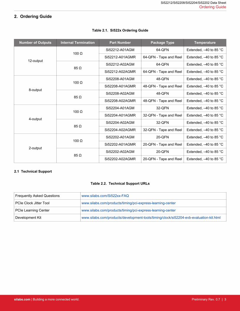
Si52202
PLL (SSC)
Control&
Memory
Divider
SCLKSDA
PWRGD/PWRDNbSS_EN
XIN/CLKIN
XOUT
DIFF[1:0]
OEb[1:0]
Figure 3.4. Si52202 Block Diagram 2-output, 20-QFN
Si52212/Si52208/Si52204/Si52202 Data SheetFunctional Block Diagrams
silabs.com | Building a more connected world. Preliminary Rev. 0.7 | 7

4. Electrical Specifications
Table 4.1. DC Electrical Specifications (VDD = 1.5 V ±5%)
Parameter Symbol Test Condition Min Typ Max Unit
1.5 V Operating Voltage VDD core 1.5 V ±5% 1.425 1.5 1.575 V
Output Supply Voltage VDDIO Supply voltage for differential LowPower outputs 0.9975 1.05–1.5 1.575 V
1.5 V Input High Voltage VIHControl input pins, except SDATA,
SCLK 0.75 VDD — VDD + 0.3 V
1.5V Input Mid Voltage VIMTri-level control input pins, except
SDATA, SCLK 0.4 VDD 0.5 VDD 0.6 VDD V
1.5 V Input Low Voltage VILControl input pins, except SDA-
TA,SCLK –0.3 — 0.25 VDD V
Input High Voltage VIHI2C SDATA, SCLK 1.14 — 3.3 V
Input Low Voltage VILI2C SDATA, SCLK — — 0.6 V
SDATA, SCLK Sink Current IPULLUP At VOL 4 — mA
Input current
IINSingle-ended inputs, VIN = GND,
VIN = VDD –5 — 5 uA
IINP
Single-ended inputs, VIN = 0 V, in-puts with internal pull-up resistorsVIN = VDD, inputs with internal
pull-down resistors
–200 — 200 uA
Input Pin Capacitance CIN 1.5 — 5 pF
Output Pin Capacitance COUT — — 6 pF
Pin Inductance LIN — — 7 nH
Si52212 Current Consumption (VDD = 1.5 V ±5%)
Power Down CurrentPWRGD/PWRDNb = "0"Byte 2, bit 2 = 0
IDD_PD_total All outputs off — 1.3 mA
IDD_PDVDD, except VDDA and VDD_IO,
all outputs off — 0.4 mA
IDD_APD VDDA, all outputs off — 0.6 mA
IDD_IOPD VDD_IO, all outputs off — 0.3 mA
Wake-on LAN CurrentPWRGD_PWRDNb = "0"Byte 2, bit 2 = 1
IDD_WOL
VDD, except VDDA and VDD_IO,all differential outputs off, REF
running— 4.0 mA
IDD_AWOLVDDA, all differential outputs off,
REF running — 0.6 mA
IDD_IOWOLVDD_IO, all differential outputs off,
REF running — 0.3 mA
Si52212/Si52208/Si52204/Si52202 Data SheetElectrical Specifications
silabs.com | Building a more connected world. Preliminary Rev. 0.7 | 8

Parameter Symbol Test Condition Min Typ Max Unit
Dynamic Supply Current
IDD_1.5V_Total
All outputs enabled. Differentialclocks with 5” traces and 2 pF
load.— 82 mA
IDD_OP
VDD, except VDDA and VDD_IO,all differential outputs active at 100
MHz— 17 mA
IDD_AOPVDDA, all differential outputs ac-
tive at 100 MHz — 7 mA
IDD_IOOPVDD_IO, all differential outputs ac-
tive at 100 MHz — 58 mA
Si52208 Current Consumption (VDD = 1.5 V ±5%)
Power Down CurrentPWRGD/PWRDNb = "0"Byte 2, bit 2 = 0
IDD_PD_total All outputs off — 1.3 mA
IDD_PDVDD, except VDDA and VDD_IO,
all outputs off — 0.4 mA
IDD_APD VDDA, all outputs off — 0.6 mA
IDD_IOPD VDD_IO, all outputs off — 0.3 mA
Wake-on LAN CurrentPWRGD_PWRDNb = "0"Byte 2, bit 2 = 1
IDD_WOL
VDD, except VDDA and VDD_IO,all differential outputs off, REF
running— 4.0 mA
IDD_AWOLVDDA, all differential outputs off,
REF running — 0.6 mA
IDD_IOWOLVDD_IO, all differential outputs off,
REF running — 0.3 mA
Dynamic Supply Current
IDD_1.5V_Total
All outputs enabled. Differentialclocks with 5” traces and 2 pF
load.— 63 mA
IDD_OP
VDD, except VDDA and VDD_IO,all differential outputs active at 100
MHz— 17 mA
IDD_AOPVDDA, all differential outputs ac-
tive at 100 MHz — 7 mA
IDD_IOOPVDD_IO, all differential outputs ac-
tive at 100 MHz — 39 mA
Si52204 Current Consumption (VDD = 1.5 V ±5%)
Power Down CurrentPWRGD/PWRDNb = "0"Byte 2, bit 2 = 0
IDD_PD_total All outputs off — 1.3 mA
IDD_PDVDD, except VDDA and VDD_IO,
all outputs off — 0.4 mA
IDD_APD VDDA, all outputs off — 0.6 mA
IDD_IOPD VDD_IO, all outputs off — 0.3 mA
Wake-on LAN CurrentPWRGD_PWRDNb = "0"Byte 2, bit 2 = 1
IDD_WOL
VDD, except VDDA and VDD_IO,all differential outputs off, REF
running— 4.0 mA
IDD_AWOLVDDA, all differential outputs off,
REF running — 0.6 mA
IDD_IOWOLVDD_IO, all differential outputs off,
REF running — 0.3 mA
Si52212/Si52208/Si52204/Si52202 Data SheetElectrical Specifications
silabs.com | Building a more connected world. Preliminary Rev. 0.7 | 9

Parameter Symbol Test Condition Min Typ Max Unit
Dynamic Supply Current
IDD_1.5V_Total
All outputs enabled. Differentialclocks with 5” traces and 2 pF
load.— 44 mA
IDD_OP
VDD, except VDDA and VDD_IO,all differential outputs active at 100
MHz— 17 mA
IDD_AOPVDDA, all differential outputs ac-
tive at 100 MHz — 7 mA
IDD_IOOPVDD_IO, all differential outputs ac-
tive at 100 MHz — 20 mA
Si52202 Current Consumption (VDD = 1.5 V ±5%)
Power Down CurrentPWRGD/PWRDNb = "0"Byte 2, bit 2 = 0
IDD_PD_total All outputs off — 1.3 mA
IDD_PDVDD, except VDDA and VDD_IO,
all outputs off — 0.4 mA
IDD_APD VDDA, all outputs off — 0.3 mA
IDD_IOPD VDD_IO, all outputs off — 0.6 mA
Wake-on LAN CurrentPWRGD_PWRDNb = "0"Byte 2, bit 2 = 1
IDD_WOL
VDD, except VDDA and VDD_IO,all differential outputs off, REF
running— 4.0 mA
IDD_AWOLVDDA, all differential outputs off,
REF running — 0.6 mA
IDD_IOWOLVDD_IO, all differential outputs off,
REF running — 0.3 mA
Dynamic Supply Current
IDD_1.5V_Total
All outputs enabled. Differentialclocks with 5” traces and 2 pF
load.— 34 mA
IDD_OP
VDD, except VDDA and VDD_IO,all differential outputs active at 100
MHz— 17 mA
IDD_AOPVDDA, all differential outputs ac-
tive at 100 MHz — 7 mA
IDD_IOOPVDD_IO, all differential outputs ac-
tive at 100 MHz — 10 mA
Si52212/Si52208/Si52204/Si52202 Data SheetElectrical Specifications
silabs.com | Building a more connected world. Preliminary Rev. 0.7 | 10

Table 4.2. DC Electrical Specifications (VDD = 1.8 V ±5%)
Parameter Symbol Test Condition Min Typ Max Unit
1.8 V Operating Voltage VDD core 1.8 V ±5% 1.71 1.8 1.89 V
Output Supply Voltage VDDIO Supply voltage for differential LowPower outputs 0.9975 1.05–1.8 1.9 V
1.8 V Input High Voltage VIHControl input pins, except SDATA,
SCLK0.75 VDD — VDD+0.3 V
1.8 V Input Mid Voltage VIMTri-level control input pins, except
SDATA, SCLK0.4 VDD 0.5 VDD 0.6 VDD V
1.8 V Input Low Voltage VILControl input pins, except SDA-
TA,SCLK -0.3 — 0.25 VDD V
Input High Voltage VIHI2C SDATA, SCLK 1.11 — 3.3 V
Input Low Voltage VILI2C SDATA, SCLK — — 0.6 V
SDATA, SCLK Sink Current IPULLUP At VOL 4 — mA
Input current
IINSingle-ended inputs, VIN = GND,
VIN = VDD –5 — 5 uA
IINP
Single-ended inputs, VIN = 0V, in-puts with internal pull-up resistorsVIN = VDD, inputs with internal
pull-down resistors
–200 — 200 uA
Input Pin Capacitance CIN 1.5 — 5 pF
Output Pin Capacitance COUT — — 6 pF
Pin Inductance LIN — — 7 nH
Si52212 Current Consumption (VDD = 1.8 V ±5%)
Power Down CurrentPWRGD/PWRDNb = "0"Byte 2, bit 3 = 0
IDD_PD_total All outputs off — 1.4 mA
IDD_PDVDD, except VDDA and VDD_IO,
all outputs off — 0.5 mA
IDD_APD VDDA, all outputs off — 0.6 mA
IDD_IOPD VDD_IO, all outputs off — 0.3 mA
Wake-on LAN CurrentPWRGD/PWRDNb = "0"Byte 2, bit 3 = 1
IDD_WOL
VDD, except VDDA and VDD_IO,all differential outputs off, REF
running— 4.5 mA
IDD_AWOLVDDA, all differential outputs off,
REF running — 0.7 mA
IDD_IOWOLVDD_IO, all differential outputs
off, REF running — 0.5 mA
Si52212/Si52208/Si52204/Si52202 Data SheetElectrical Specifications
silabs.com | Building a more connected world. Preliminary Rev. 0.7 | 11

Parameter Symbol Test Condition Min Typ Max Unit
Dynamic Supply Current
IDD_1.8V_Total
All outputs enabled. Differentialclocks with 5” traces and 2 pF
load.— 84 mA
IDD_OP
VDD, except VDDA and VDD_IO,all differential outputs active at
100 MHz— 19 mA
IDD_AOPVDDA, all differential outputs ac-
tive at 100 MHz — 7 mA
IDD_IOOPVDD_IO, all differential outputs
active at 100 MHz — 58 mA
Si52208 Current Consumption (VDD = 1.8 V ±5%)
Power Down CurrentPWRGD/PWRDNb = ''0"Byte 2, bit 3 = 0
IDD_PD_total All outputs off — 1.4 mA
IDD_PDVDD, except VDDA and VDD_IO,
all outputs off — 0.5 mA
IDD_APD VDDA, all outputs off — 0.6 mA
IDD_IOPD VDD_IO, all outputs off — 0.3 mA
Wake-on LAN CurrentPWRGD/PWRDNb = "0"Byte 2, bit 3 = 1
IDD_WOL
VDD, except VDDA and VDD_IO,all differential outputs off, REF
running— 4.5 mA
IDD_AWOLVDDA, all differential outputs off,
REF running — 0.7 mA
IDD_IOWOLVDD_IO, all differential outputs
off, REF running — 0.5 mA
Dynamic Supply Current
IDD_1.8V_Total
All outputs enabled. Differentialclocks with 5” traces and 2 pF
load.— 65 mA
IDD_OP
VDD, except VDDA and VDD_IO,all differential outputs active at
100 MHz— 19 mA
IDD_AOPVDDA, all differential outputs ac-
tive at 100 MHz — 7 mA
IDD_IOOPVDD_IO, all differential outputs
active at 100 MHz — 39 mA
Si52204 Current Consumption (VDD = 1.8 V ±5%)
Power Down CurrentPWRGD/PWRDNb = "0"Byte 2, bit 3 = 0
IDD_PD_total All outputs off — 1.4 mA
IDD_PDVDD, except VDDA and VDD_IO,
all outputs off — 0.5 mA
IDD_APD VDDA, all outputs off — 0.6 mA
IDD_IOPD VDD_IO, all outputs off — 0.3 mA
Wake-on LAN CurrentPWRGD/PWRDNb = ''0"Byte 2, bit 3 = 1
IDD_WOL
VDD, except VDDA and VDD_IO,all differential outputs off, REF
running— 4.5 mA
IDD_AWOLVDDA, all differential outputs off,
REF running — 0.7 mA
IDD_IOWOLVDD_IO, all differential outputs
off, REF running — 0.5 mA
Si52212/Si52208/Si52204/Si52202 Data SheetElectrical Specifications
silabs.com | Building a more connected world. Preliminary Rev. 0.7 | 12

Parameter Symbol Test Condition Min Typ Max Unit
Dynamic Supply Current
IDD_1.8V_Total
All outputs enabled. Differentialclocks with 5” traces and 2 pF
load.— 46 mA
IDD_OP
VDD, except VDDA and VDD_IO,all differential outputs active at
100 MHz— 19 mA
IDD_AOPVDDA, all differential outputs ac-
tive at 100 MHz — 7 mA
IDD_IOOPVDD_IO, all differential outputs
active at 100 MHz — 20 mA
Si52202 Current Consumption (VDD = 1.8 V ±5%)
Power Down CurrentPWRGD/PWRDNb = "0"Byte 2, bit 3 = 0
IDD_PD_total All outputs off — 1.4 mA
IDD_PDVDD, except VDDA and VDD_IO,
all outputs off — 0.5 mA
IDD_APD VDDA, all outputs off — 0.6 mA
IDD_IOPD VDD_IO, all outputs off — 0.3 mA
Wake-on LAN CurrentPWRGD/PWRDNb = ''0"Byte 2, bit 2 = 1
IDD_WOL
VDD, except VDDA and VDD_IO,all differential outputs off, REF
running— 4.5 mA
IDD_AWOLVDDA, all differential outputs off,
REF running — 0.7 mA
IDD_IOWOLVDD_IO, all differential outputs
off, REF running — 0.5 mA
Dynamic Supply Current
IDD_1.8V_Total
All outputs enabled. Differentialclocks with 5” traces and 2 pF
load.— 36 mA
IDD_OP
VDD, except VDDA and VDD_IO,all differential outputs active at
100 MHz— 19 mA
IDD_AOPVDDA, all differential outputs ac-
tive at 100 MHz — 7 mA
IDD_IOOPVDD_IO, all differential outputs
active at 100 MHz — 10 mA
Si52212/Si52208/Si52204/Si52202 Data SheetElectrical Specifications
silabs.com | Building a more connected world. Preliminary Rev. 0.7 | 13

Table 4.3. AC Electrical Specifications
Parameter Symbol Condition Min Typ Max Unit
Clock Input
CLKIN Frequency — 25 MHz
CLKIN Duty Cycle TDC Measured at VDD/2 45 — 55 %
CLKIN Rising and FallingSlew Rate
TR/TFMeasured between 0.2 VDD and
0.8 VDD 0.5 — 4 V/ns
Input High Voltage VIH XIN/CLKIN pin 0.75 VDD — V
Input Low Voltage VIL XIN/CLKIN pin — — 0.25 VDD V
Input Common Mode VCOM Common mode input voltage 300 — 1000 mV
Input Amplitude VSWING Peak to Peak value 300 — 1450 mV
Control Input Pins
Trise TrRise time of single-ended control
inputs — — 5 ns
Tfall TfFall time of single-ended control
inputs — — 5 ns
SDATA, SCLK Rise Time TrI2C(Max VIL – 0.15) to
(Min VIH + 0.15) — — 1000 ns
SDATA, SCLK Fall Time TfI2C(Min VIH + 0.15) to(Max VIL – 0.15) — — 300 ns
SMBus OperatingFrequency
FmaxI2CMaximum SMBus operating
frequency — — 400 kHz
LVCMOS – REF (VDD = 1.5 V ±5%)
Long Accuracy ppm Variation from referencefrequency 0 ppm
Clock Period TPERIOD 25 MHz output — 40 ns
Slew Rate
TrfByte 2[1:0] = 48 (Slowest), 20% to
80% of VDDREF — 0.5 V/ns
Byte 2[1:0] = 49 (Slow), 20% to80% of VDDREF — 0.7 V/ns
Byte 2[1:0] = 4A (Fast), 20% to80% of VDDREF — 0.9 V/ns
Byte 2[1:0] = 4B (Fastest), 20% to80% of VDDREF — 0.9 V/ns
Duty Cycle1 TDC_REF VT = VDD/2 V 45 50 55 %
Cycle-to-Cycle Jitter TCCJ_REF VT = VDD/2 V — 45 ps
Phase Jitter RMSREF 12 kHz to 5MHz — 0.35 ps
REF Noise Floor TJ1kHz_REF 1 kHz offset — –132 dBc
REF Noise Floor TJ10kHz_REF 10 kHz offset to Nyquist — –143 dBc
Si52212/Si52208/Si52204/Si52202 Data SheetElectrical Specifications
silabs.com | Building a more connected world. Preliminary Rev. 0.7 | 14

Parameter Symbol Condition Min Typ Max Unit
LVCMOS – REF (VDD = 1.8 V ±5%)
Long Accuracy ppm Variation from referencefrequency 0 ppm
Clock Period TPERIOD 25 MHz output — 40 ns
Slew Rate
TrfByte 2[1:0] = 48 (Slowest), 20% to
80% of VDDREF — 0.7 V/ns
Byte 2[1:0] = 49 (Slow), 20% to80% of VDDREF — 1.0 V/ns
Byte 2[1:0] = 4A (Fast), 20% to80% of VDDREF — 1.2 V/ns
Byte 2[1:0] = 4B (Fastest), 20% to80% of VDDREF — 1.3 V/ns
Duty Cycle1 TDC_REF VT = VDD/2 V 45 50 55 %
Cycle-to-Cycle Jitter TCCJ_REF VT = VDD/2 V — 30 ps
Phase Jitter RMSREF 12 kHz to 5 MHz — 0.32 ps
REF Noise Floor TJ1kHz_REF 1 kHz offset — –132 dBc
REF Noise Floor TJ10kHz_REF 10 kHz offset to Nyquist — –145 dBc
DIFF HCSL
Duty Cycle TDC Measured at 0 V differential 45 50 55 %
Output-to-Output Skew TSKEW Measured at 0 V differential — 10 ps
Slew Rate TR/TF
Measured differentially from±150 mV (fast setting) — 2.3 V/ns
Measured differentially from±150 mV (slow setting) — 1.8 V/ns
Slew Rate Matching Delta TR/TF — 2 %
Max modulation frequencydf/dt
Tmax-freqmod-
slew— — 1250 ppm/usec
Voltage High VHIGH 600 — 850 mV
Voltage Low VLOW –150 — 150 mV
Max Voltage VMAX — 750 1150 mV
Min Voltage VMIN –300 0 mV
Crossing Point Voltage VOXAbsolute crossing point voltage at
0.7 V Swing 250 — 550 mV
Crossing Point Voltage (var) VOX_DELTAVariation of VOX over all rising
clock edges — 35 mV
Modulation Frequency FMOD 30 31.5 33 kHz
Enable/Disable and Setup
Clock Stabilization fromPower-up
TSTABLE — 1 ms
Si52212/Si52208/Si52204/Si52202 Data SheetElectrical Specifications
silabs.com | Building a more connected world. Preliminary Rev. 0.7 | 15

Parameter Symbol Condition Min Typ Max Unit
OE_b Latency TOEBLAT
Differential outputs start afterOE_b assertion Differential out-
puts stop after OE_b deassertion— 2 clocks
PD_b Latency to differentialoutputs enable
TPDbDifferential outputs enable after
PD_b de-assertion — 490 µs
Note:1. This is for XTAL mode only. For CLKIN mode, there would be a duty cycle distortion spec of ±0.5 ns.
Si52212/Si52208/Si52204/Si52202 Data SheetElectrical Specifications
silabs.com | Building a more connected world. Preliminary Rev. 0.7 | 16

Table 4.4. PCIe and Intel QPI Jitter Specifications
Parameter Symbol Condition Min Typ Max JitterLimit Unit
DIFF HCSL
Cycle to Cycle Jitter JCCJ Measured at 0 V differential — 23 ps(pk-pk)
PCIe Gen 1 Pk-Pk Jitter JPk-Pk PCIe Gen 1 0 21 86 ps(pk-pk)
PCIe Gen 2 Phase Jitter JRMSGEN2
10 kHz < F < 1.5 MHz 0 0.9 3 ps(RMS)
1.5 MHz < F < Nyquist 0 1.4 3.1 ps(RMS)
PCIe Gen 3 Phase Jitter JRMSGEN3Includes PLL BW 2–4 MHz,
CDR = 10 MHz — 0.3 0.4 1.0 ps(RMS)
PCIe Gen 3 SRIS1
Phase JitterJRMSGen3_SRIS
Includes PLL BW 2–4 MHz,CDR = 10 MHz — 0.39 0.5 0.7 ps
(RMS)
PCIe Gen 4 Phase Jitter JRMSGen4Includes PLL BW 2–4 MHz,
CDR = 10 MHz — 0.3 0.4 0.5 ps(RMS)
PCIe Gen 4 SRIS1
Phase JitterJRMSGen4_SRIS
Includes PLL BW 2–4 MHz,CDR = 10 MHz — 0.41 0.5 0.5 ps
(RMS)
Intel QPI Specifications for 100 MHz and 133 MHz
Intel QPI and SMI REFCLKaccummulated jitter2, 3, 4 JRMSQPI_SMI 8 Gb/s, 100 MHz, 12UI — 0.13 ps
(RMS)
Intel QPI and SMI REFCLKaccummulated jitter2, 3, 4 JRMSQPI_SMI 9.6 Gb/s, 100 MHz, 12UI — 0.11 ps
(RMS)
Intel QPI and SMI REFCLKaccummulated jitter2, 3, 4 JRMSQPI_SMI 4.8 Gb/s, 133 MHz, 12UI, 17.04M — 0.4 ps
(RMS)
Intel QPI and SMI REFCLKaccummulated jitter2, 3, 4 JRMSQPI_SMI 4.8 Gb/s, 133 MHz, 12UI, 7.8M — 0.2 ps
(RMS)
Intel QPI and SMI REFCLKaccummulated jitter2, 3, 4 JRMSQPI_SMI 6.4 Gb/s, 133 MHz, 12UI, 17.04M — 0.3 ps
(RMS)
Intel QPI & SMI REFCLKaccummulated jitter2, 3, 4 JRMSQPI_SMI 6.4 Gb/s, 133 MHz, 12UI, 7.8M — 0.15 ps
(RMS)
Note:1. The SRIS jitter limit is the system RefClk simulation budget divided by sqrt (2) for equal allocation of uncorrelated jitter between
two clocks.2. Post processed evaluation through Intel supplied Matlab scripts3. Measuring on 100 MHz output using the template file in the PCIe Jitter Tool4. Measuring on 100 MHz, 133 MHz outputs using the template file in the PCIe Jitter Tool. Visit www.pcisig.com for complete PCIe
specifications.
Si52212/Si52208/Si52204/Si52202 Data SheetElectrical Specifications
silabs.com | Building a more connected world. Preliminary Rev. 0.7 | 17

Table 4.5. Absolute Maximum Conditions
Parameter Symbol Test Condition Min Typ Max Unit
Main Supply Voltage VDD_1.8V Functional — — 2.5 V
Input Voltage VIN Relative to VSS –0.5 — VDD + 0.5 V
Input High Voltage I2C VIH_I2C SDATA and SCLK — 3.6 V
Temperature, Storage TS Non-functional –65 — 150 Celsius
Temperature, Operating Ambient TA Functional –40 — 85 Celsius
Temperature, Junction TJ Functional — — 150 Celsius
Dissipation, Junction to Case θJC JEDEC(JESD 51)
— — 22 Celsius/W
Dissipation, Junction to Ambient θJA JEDEC(JESD 51)
— — 30 Celsius/W
ESD Protection(Human Body Model)
ESDHBM JEDEC(JESD 22-A114)
–2000 — 2000 V
Flammability Rating UL-94 UL (Class) V–0
Note: While using multiple power supplies, the voltage on any input or I/O pin cannot exceed the power pin during power-up. Powersupply sequencing is not required.
Si52212/Si52208/Si52204/Si52202 Data SheetElectrical Specifications
silabs.com | Building a more connected world. Preliminary Rev. 0.7 | 18
5. Functional Description
5.1 Crystal Recommendations
The clock device requires a parallel resonance crystal.
Table 5.1. Crystal Recommendations
Frequency(Fund)
Cut Loading Load Cap Shunt Cap(max)
Motional(max)
Tolerance(max)
Stability(max)
Aging (max)
25 MHz AT Parallel 8–15 pF 5 pF 0.016 pF 35 ppm 30 ppm 5 ppm
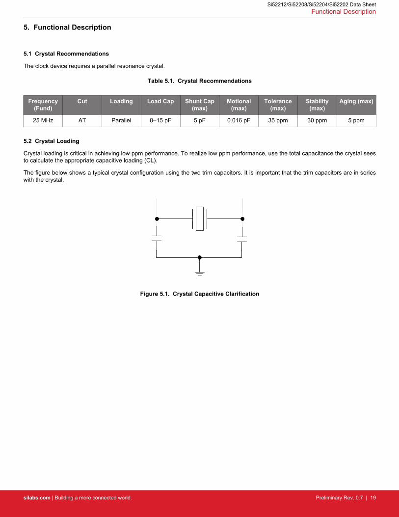
5.2 Crystal Loading
Crystal loading is critical in achieving low ppm performance. To realize low ppm performance, use the total capacitance the crystal seesto calculate the appropriate capacitive loading (CL).
The figure below shows a typical crystal configuration using the two trim capacitors. It is important that the trim capacitors are in serieswith the crystal.
Figure 5.1. Crystal Capacitive Clarification
Si52212/Si52208/Si52204/Si52202 Data SheetFunctional Description
silabs.com | Building a more connected world. Preliminary Rev. 0.7 | 19

5.3 Calculating Load Capacitors
In addition to the standard external trim capacitors, consider the trace capacitance and pin capacitance to calculate the crystal loadingcorrectly. Again, the capacitance on each side is in series with the crystal. The total capacitance on both sides is twice the specifiedcrystal load capacitance (CL). Trim capacitors are calculated to provide equal capacitive loading on both sides.
Figure 5.2. Crystal Loading Example
Use the following formulas to calculate the trim capacitor values for Ce1 and Ce2:
Load Capacitance (each side)
Ce = 2 × CL − (Cs + Ci)
Total Capacitance (as seen by the crystal)
CLe = 1
( 1Ce + Cs1 + Ci1 + 1
Ce2 + Cs2 + Ci2 )
• CL: Crystal load capacitance• CLe: Actual loading seen by crystal using standard value trim capacitors• Ce: External trim capacitors• Cs: Stray capacitance (terraced)• Ci : Internal capacitance (lead frame, bond wires, etc.)
Si52212/Si52208/Si52204/Si52202 Data SheetFunctional Description
silabs.com | Building a more connected world. Preliminary Rev. 0.7 | 20

5.4 PWRGD/PWRDNb (Power Down) Pin
The PWRGD/PWRDNb pin is a dual-function pin. During initial power up, the pin functions as the PWRGD pin. Upon the first power up,if the PWRGD pin is low, the outputs will be disabled, but the crystal oscillator and I2C logics will be active. Once the PWRGD pin hasbeen sampled high by the clock chip, the pin assumes a PWRDNb functionality. When the pin has assumed a PWRDNb functionalityand is pulled low, the device will be placed in power down mode. The PWRGD/PWRDNb pin is required to be driven at all times. Theassertion and dessertion of PWRDNb is asynchronous.
Tstable<1.8 ms
Tdrive_Pwrdn#<300 µs; > 200 mV
DIF
DIF
PWRDWN
Figure 5.3. Differential (CLOCK–CLOCK) Measurement Points (Tperiod, Duty Cycle, Jitter)
5.5 PWRDNb (Power Down) Assertion
The PDB pin is an asynchronous active low input used to disable all output clocks in a glitch-free manner. All outputs will be driven lowin power down mode. In power down mode, all outputs, the crystal oscillator, and the I2C logic are disabled.
PWRDWN
DIF
DIF
Figure 5.4. PWRDNb Assertion
5.6 PWRDNb (Power Down) Deassertion
When a valid rising edge on PWRGD/PWRDNb pin is applied, all outputs are enabled in a glitch-free manner within two to six outputclock cycles.
5.7 OEb Pin
The OEb pin is an active low input used to enable and disable the output clock. To enable the output clock, the OEb pin needs to belogic low, and I2C OE bit needs to be logic high. By default, the OEb pin is set to logic low, and I2C OE bit is set to logic high.There aretwo methods to disable the output clock: the OEb pin is pulled to a logic high, or the I2C OEb bit is set to a logic low. The OEb pin isrequired to be driven at all times.
5.8 OEb Assertion
The OEb pin is an active low input used for synchronous stopping and starting the respective output clock while the rest of the clockgenerator continues to function. The assertion of the OEb function is achieved by pulling the OEb pin low while the I2C OE bit is high,which causes the respective stopped output to resume normal operation. No short or stretched clock pulses are produced when theclocks resume. The maximum latency from the assertion to active outputs is no more than two to six output clock cycles.
5.9 OEb Deassertion
The OEb function is deasserted by pulling high or writing the I2C OE bit to a logic low. The corresponding output is stopped cleanly andthe final output state is driven low.
Si52212/Si52208/Si52204/Si52202 Data SheetFunctional Description
silabs.com | Building a more connected world. Preliminary Rev. 0.7 | 21

5.10 FS Pin
The FS pin will select 0 = 100 MHz, mid = 200 MHz, 1 = 133 MHz. This is a tri-state pin, and this pin has a weak internal pull-down ofapproximately 100 kΩ.
The default output frequency is 100 MHz.
The following figure shows the recommended configurations for tri-state.
VDD
R1
R2
FS Pin
Static OptionThe user can NP either R1, R2, or neither to constantly maintain low, high, or mid levels, respectively.
VDD
FS Pin
Tri-State Dynamic OptionThe user can use an MCU with strong Tri-State outputs to drive the FS pin. 1 k-ohm resistors should be adequate for most MCU drivers; however, the resistance can be increased to compensate for a weaker driver. Increasing the resistors will increase noise levels on the FS pin line.
MCUWith Tri-State Outputs
Outputs0, High Z and VDD
MCUWith Tri-State Outputs
Outputs0, VDD/2 and VDD
FS Pin
3-Level Dynamic OptionAn MCU with a 3-level output capability can be directly connected to the FS Pin.
1 k
1 k
1 k
1 kR1
R2
Figure 5.5. Si522xx FS Tri-State Pin Circuit Configuration Suggestions
Si52212/Si52208/Si52204/Si52202 Data SheetFunctional Description
silabs.com | Building a more connected world. Preliminary Rev. 0.7 | 22

6. Test and Measurement Setup
The following diagrams show the test load configuration for the differential clock signals.
MeasurementPoint
2 pF50
MeasurementPoint
2 pF50
L1
L1 = 5"
OUT+
OUT-L1
Figure 6.1. 0.7 V Differential Load Configuration
Figure 6.2. Differential Output Signals (for AC Parameters Measurement)
Si52212/Si52208/Si52204/Si52202 Data SheetTest and Measurement Setup
silabs.com | Building a more connected world. Preliminary Rev. 0.7 | 23
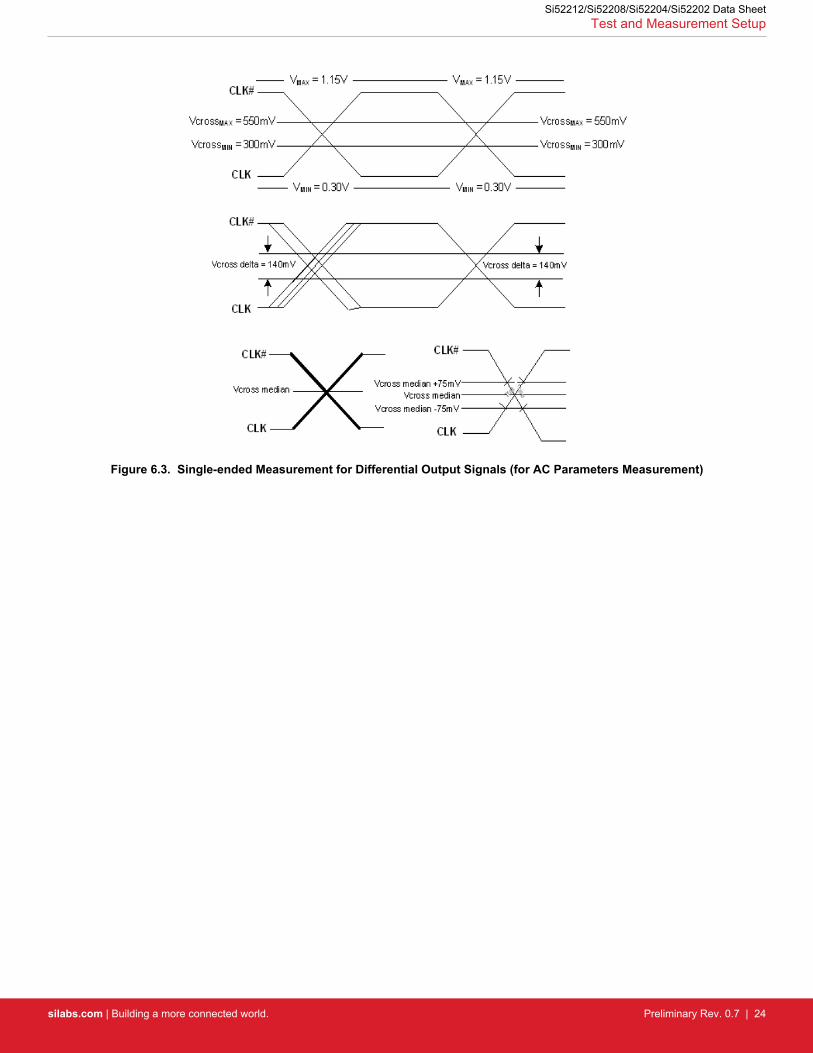
Figure 6.3. Single-ended Measurement for Differential Output Signals (for AC Parameters Measurement)
Si52212/Si52208/Si52204/Si52202 Data SheetTest and Measurement Setup
silabs.com | Building a more connected world. Preliminary Rev. 0.7 | 24

7. PCIe Clock Jitter Tool
The PCIe Clock Jitter Tool is designed to enable users to quickly and easily take jitter measurements for PCIe Gen1/2/3/4 and SRNS/SRIS. This software removes all the guesswork for PCIe Gen1/2/3/4 and SRNS/SRIS jitter measurements and margins in board de-signs. This software tool will provide accurate results in just a few clicks, and is provided in an executable format to support variouscommon input waveform files, such as .csv, .wfm, and .bin. The easy-to-use GUI and helpful tips guide users through each step. Re-lease notes and other documentation are also included in the software package.
Download it for free at http://www.silabs.com/pcie-learningcenter.
Figure 7.1. PCIe Clock Jitter Tool
Si52212/Si52208/Si52204/Si52202 Data SheetPCIe Clock Jitter Tool
silabs.com | Building a more connected world. Preliminary Rev. 0.7 | 25

8. Control Registers
8.1 I2C Interface
To enhance the flexibility and function of the clock synthesizer, an I2C interface is provided. Through the I2C interface, various devicefunctions, such as individual clock output buffers, are individually enabled or disabled. The registers associated with the I2C interfaceinitialize to their default setting at power-up. The use of this interface is optional. Clock device register changes are normally made atsystem initialization, if any are required.
8.2 Block Read/Write
The clock driver I2C protocol accepts block write and block read operations from the controller. For block write/read operation, accessthe bytes in sequential order from lowest to highest (most significant bit first) with the ability to stop after any complete byte is transfer-red. The block write and block read protocol is outlined in Table 8.2 Block Read and Block Write Protocol on page 29.
8.3 Block Read
After the slave address is sent with the R/W condition bit set, the command byte is sent with the MSB = 0. The slave acknowledges theregister index in the command byte. The master sends a repeat start function. After the slave acknowledges this, the slave sends thenumber of bytes it wants to transfer (>0 and <33). The master acknowledges each byte except the last and sends a stop function.
SlaveT Wr A Command Code
CommandstarTCondition
Block Read Protocol
Acknowledgerepeat starTRegister # to
readMSB = 0
1 7 1 1 8
Master to
Slave to
Slave ARdA r1 1 7 11
Data Byte A Data Byte 0 A Data Byte 1 N P8 1 8 1 8 1 1
Not acknowledgestoP Condition
Figure 8.1. Block Read Protocol
Si52212/Si52208/Si52204/Si52202 Data SheetControl Registers
silabs.com | Building a more connected world. Preliminary Rev. 0.7 | 26
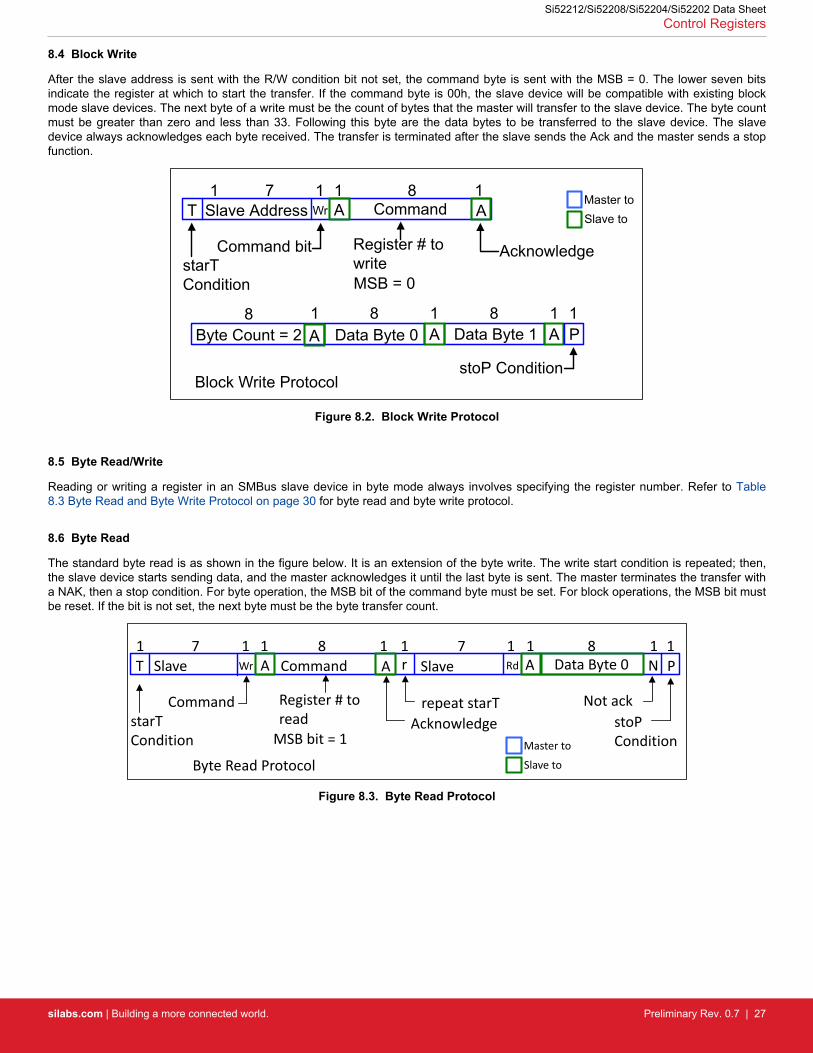
8.4 Block Write
After the slave address is sent with the R/W condition bit not set, the command byte is sent with the MSB = 0. The lower seven bitsindicate the register at which to start the transfer. If the command byte is 00h, the slave device will be compatible with existing blockmode slave devices. The next byte of a write must be the count of bytes that the master will transfer to the slave device. The byte countmust be greater than zero and less than 33. Following this byte are the data bytes to be transferred to the slave device. The slavedevice always acknowledges each byte received. The transfer is terminated after the slave sends the Ack and the master sends a stopfunction.
Slave AddressT Wr A Command
Command bitstarTCondition
Block Write Protocol
AcknowledgeRegister # to writeMSB = 0
1 7 1 1 8 Master toSlave toA
1
Data Byte 0 A Data Byte 1 A P1 8 1 8 1 1
stoP Condition
Byte Count = 2 A8
Figure 8.2. Block Write Protocol
8.5 Byte Read/Write
Reading or writing a register in an SMBus slave device in byte mode always involves specifying the register number. Refer to Table8.3 Byte Read and Byte Write Protocol on page 30 for byte read and byte write protocol.
8.6 Byte Read
The standard byte read is as shown in the figure below. It is an extension of the byte write. The write start condition is repeated; then,the slave device starts sending data, and the master acknowledges it until the last byte is sent. The master terminates the transfer witha NAK, then a stop condition. For byte operation, the MSB bit of the command byte must be set. For block operations, the MSB bit mustbe reset. If the bit is not set, the next byte must be the byte transfer count.
SlaveT Wr A Command Slave ARd Data Byte 0 N PA r
CommandstarTCondition
Byte Read Protocol
Acknowledgerepeat starT Not ack
stoPCondition
Register # to read
MSB bit = 1
1 7 1 1 8 1 1 7 11 8 1 1
Master to
Slave to
Figure 8.3. Byte Read Protocol
Si52212/Si52208/Si52204/Si52202 Data SheetControl Registers
silabs.com | Building a more connected world. Preliminary Rev. 0.7 | 27

8.7 Byte Write
The figure below illustrates a simple, typical byte write. For byte operation, the MSB bit of the command byte must be set. For blockoperations, the MSB bit must be reset. If the bit is not set, the next byte must be the byte transfer count. The count can be between 1and 32. It is not allowed to be zero or to exceed 32.
SlaveT Wr A Command Data Byte 0A
CommandstarT Condition
Byte Write Protocol
AcknowledgeRegister # to write
MSB bit = 1
1 7 1 1 8 1 8 11
Master to
Slave to
A P
stoP Condition
Figure 8.4. Byte Write Protocol
Si52212/Si52208/Si52204/Si52202 Data SheetControl Registers
silabs.com | Building a more connected world. Preliminary Rev. 0.7 | 28

8.8 Data Protocol
The clock driver I2C protocol accepts byte write, byte read, block write, and block read operations from the controller. For block write/read operation, access the bytes in sequential order from lowest to highest (most significant bit first) with the ability to stop after anycomplete byte is transferred. For byte write and byte read operations, the system controller can access individually indexed bytes. Theblock write and block read protocol is outlined in Table 8.2 Block Read and Block Write Protocol on page 29 while Table 8.3 ByteRead and Byte Write Protocol on page 30 outlines byte write and byte read protocol.
Table 8.1. SA State on First Application of PWRGD/PWRDNb
Description SA Address
State of SA on first application of PWRGD/PWRDNb1 0 1101001
1 1101010
Note:1. Si52202 default address is 0x6A
Table 8.2. Block Read and Block Write Protocol
Block Write Protocol Block Read Protocol
Bit Description Bit Description
1 Start 1 Start
8:2 Slave address—7 bits 8:2 Slave address–7 bits
9 Write 9 Write
10 Acknowledge from slave 10 Acknowledge from slave
18:11 Command Code—8 bits 18:11 Command Code–8 bits
19 Acknowledge from slave 19 Acknowledge from slave
27:20 Byte Count—8 bits 20 Repeat start
28 Acknowledge from slave 27:21 Slave address–7 bits
36:29 Data byte 1–8 bits 28 Read = 1
37 Acknowledge from slave 29 Acknowledge from slave
45:38 Data byte 2–8 bits 37:30 Byte Count from slave–8 bits
46 Acknowledge from slave 38 Acknowledge
.... Data Byte/Slave Acknowledges 46:39 Data byte 1 from slave–8 bits
.... Data Byte N–8 bits 47 Acknowledge
.... Acknowledge from slave 55:48 Data byte 2 from slave–8 bits
.... Stop 56 Acknowledge
.... Data bytes from slave/Acknowl-edge
.... Data Byte N from slave–8 bits
.... NOT Acknowledge
.... Stop
Si52212/Si52208/Si52204/Si52202 Data SheetControl Registers
silabs.com | Building a more connected world. Preliminary Rev. 0.7 | 29

Table 8.3. Byte Read and Byte Write Protocol
Byte Write Protocol Byte Read Protocol
Bit Description Bit Description
1 Start 1 Start
8:2 Slave address–7 bits 8:2 Slave address–7 bits
9 Write 9 Write
10 Acknowledge from slave 10 Acknowledge from slave
18:11 Command Code–8 bits 18:11 Command Code–8 bits
19 Acknowledge from slave 19 Acknowledge from slave
27:20 Data byte–8 bits 20 Repeated start
28 Acknowledge from slave 27:21 Slave address–7 bits
29 Stop 28 Read
29 Acknowledge from slave
37:30 Data from slave–8 bits
38 NOT Acknowledge
39 Stop
Si52212/Si52208/Si52204/Si52202 Data SheetControl Registers
silabs.com | Building a more connected world. Preliminary Rev. 0.7 | 30

8.9 Register Tables
8.9.1 Si52212 Registers
Table 8.4. Control Register 0. Byte 0
Bit Name If Bit = 0 If Bit = 1 Type Default Function
7 DIFF7_OE Disabled Enabled RW 1 Output enable for DIFF[7]
6 DIFF6_OE Disabled Enabled RW 1 Output enable for DIFF[6]
5 DIFF5_OE Disabled Enabled RW 1 Output enable for DIFF[5]
4 DIFF4_OE Disabled Enabled RW 1 Output enable for DIFF[4]
3 DIFF3_OE Disabled Enabled RW 1 Output enable for DIFF[3]
2 DIFF2_OE Disabled Enabled RW 1 Output enable for DIFF[2]
1 DIFF1_OE Disabled Enabled RW 1 Output enable for DIFF[1]
0 DIFF0_OE Disabled Enabled RW 1 Output enable for DIFF[0]
Table 8.5. Control Register 1. Byte 1
Bit Name If Bit = 0 If Bit = 1 Type Default Function
7 DIFF11_OE Disabled Enabled RW 1 Output enable for DIFF[11]
6 DIFF10_OE Disabled Enabled RW 1 Output enable for DIFF[10]
5 DIFF9_OE Disabled Enabled RW 1 Output enable for DIFF[9]
4 DIFF8_OE Disabled Enabled RW 1 Output enable for DIFF[8]
3Reserved
0Reserved
2 0
1 SS_EN_READ1 R 0 Spread Enable software readback00 = –0.25%; 01 = –0.5%; 10 =
OFF; 11 = –0.5%0 SS_EN_READ0 R 0
Table 8.6. Control Register 2. Byte 2
Bit Name If Bit = 0 If Bit = 1 Type Default Function
7 SS_EN_SW_HW_CTRL Read back Byte1[1:0]
SS control byByte 2 [6:5] RW 0 Enable software control of spread
6 SS_EN_SW1 RW 0 Software control of spread 00 = –0.25%; 01 = OFF; 10 = OFF; 11 = –0.5%5 SS_EN_SW0 RW 1
4 Reserved 0 Reserved
3 REF_OE Disabled Enabled RW 1 Output Enable for REF
2 REF PWRDNREF output is
disabled in Pow-er Down.
REF output isenabled in Pow-
er DownRW 0
Wake-on LAN for REF. To have REFoutput enabled in Power Down,REF_OE needs to be enabled at thesame time.
Si52212/Si52208/Si52204/Si52202 Data SheetControl Registers
silabs.com | Building a more connected world. Preliminary Rev. 0.7 | 31

Bit Name If Bit = 0 If Bit = 1 Type Default Function
1REF_SLR
RW 0 REF Output Slew Rate Control 00 =Slowest; 01 = Slow; 10 = Fast; 11 =Fastest0 RW 1
Table 8.7. Control Register 3. Byte 3
Bit Name If Bit = 0 If Bit = 1 Type Default Function
7 SR_SEL_DIFF7 Slow setting Fast setting RW 1 Slew rate control for DIFF7
6 SR_SEL_DIFF6 Slow setting Fast setting RW 1 Slew rate control for DIFF6
5 SR_SEL_DIFF5 Slow setting Fast setting RW 1 Slew rate control for DIFF5
4 SR_SEL_DIFF4 Slow setting Fast setting RW 1 Slew rate control for DIFF4
3 SR_SEL_DIFF3 Slow setting Fast setting RW 1 Slew rate control for DIFF3
2 SR_SEL_DIFF2 Slow setting Fast setting RW 1 Slew rate control for DIFF2
1 SR_SEL_DIFF1 Slow setting Fast setting RW 1 Slew rate control for DIFF1
0 SR_SEL_DIFF0 Slow setting Fast setting RW 1 Slew rate control for DIFF0
Table 8.8. Control Register 4. Byte 4
Bit Name If Bit = 0 If Bit = 1 Type Default Function
7 SR_SEL_DIFF11 Slow setting Fast setting RW 1 Slew rate control for DIFF11
6 SR_SEL_DIFF10 Slow setting Fast setting RW 1 Slew rate control for DIFF10
5 SR_SEL_DIFF9 Slow setting Fast setting RW 1 Slew rate control for DIFF9
4 SR_SEL_DIFF8 Slow setting Fast setting RW 1 Slew rate control for DIFF8
3 AMP RW 0
Controls Output Amplitude2 AMP RW 0
1 AMP RW 0
0 AMP RW 0
Table 8.9. Control Register 5. Byte 5
Bit Name If Bit = 0 If Bit = 1 Type Default Function
7
Rev Code [7:4]
R 0
Revision Code6 R 0
5 R 0
4 R 0
3
Vendor ID[3:0]
R 1
Vendor Identification Code2 R 0
1 R 0
0 R 0
Si52212/Si52208/Si52204/Si52202 Data SheetControl Registers
silabs.com | Building a more connected world. Preliminary Rev. 0.7 | 32

Table 8.10. Control Register 6. Byte 6
Bit Name If Bit = 0 If Bit = 1 Type Default Function
7
Programming ID [7:0]
R 0
Programming ID (Internal Only)
6 R 0
5 R 0
4 R 0
3 R 0
2 R 0
1 R 0
0 R 0
Table 8.11. Control Register 7. Byte 7
Bit Name If Bit = 0 If Bit = 1 Type Default Function
7 BC R 0 Byte Count
6 BC R 0 Byte Count
5 BC R 0 Byte Count
4 BC R 0 Byte Count
3 BC R 1 Byte Count
2 BC R 0 Byte Count
1 BC R 0 Byte Count
0 BC R 0 Byte Count
Si52212/Si52208/Si52204/Si52202 Data SheetControl Registers
silabs.com | Building a more connected world. Preliminary Rev. 0.7 | 33

8.9.2 Si52208 Registers
Table 8.12. Control Register 0. Byte 0
Bit Name If Bit = 0 If Bit = 1 Type Default Function
7 Reserved 0 Reserved
6 DIFF4_OE Disabled Enabled RW 1 Output enable for DIFF_4
5 DIFF3_OE Disabled Enabled RW 1 Output enable for DIFF_3
4 Reserved 0 Reserved
3 Reserved 0 Reserved
2 DIFF2_OE Disabled Enabled RW 1 Output enable for DIFF_2
1 DIFF1_OE Disabled Enabled RW 1 Output enable for DIFF_1
0 DIFF0_OE Disabled Enabled RW 1 Output enable for DIFF_0
Table 8.13. Control Register 1. Byte 1
Bit Name If Bit = 0 If Bit = 1 Type Default Function
7 DIFF7_OE Disabled Enabled RW 1 Output enable for DIFF_7
6 DIFF6_OE Disabled Enabled RW 1 Output enable for DIFF_6
5 Reserved 0 Reserved
4 DIFF5_OE Disabled Enabled RW 1 Output enable for DIFF_5
3Reserved
0Reserved
2 0
1 SS_EN_READ1 R 0 Spread Enable software readback00 = –0.25%; 01 = –0.5%; 10 =
OFF; 11 = –0.5%0 SS_EN_READ0 R 0
Table 8.14. Control Register 2. Byte 2
Bit Name If Bit = 0 If Bit = 1 Type Default Function
7 SS_EN_SW_HW_CTRL Read back Byte1[1:0]
SS control byByte 2 [6:5] RW 0 Enable software control of spread
6 SS_EN_SW1 RW 0 Software control of spread 00 = –0.25%; 01 = OFF; 10 = OFF; 11 = –
0.5%5 SS_EN_SW0 RW 1
4 Reserved 0 Reserved
3 REF_OE Disabled Enabled RW 1 Output Enable for REF
2 REF PWRDNREF output is
disabled in Pow-er Down.
REF output isenabled in Pow-
er DownRW 0
Wake-on LAN for REF. To have REFoutput enabled in Power Down,
REF_OE needs to be enabled at thesame time.
1REF_SLR
RW 0 REF Output Slew Rate Control 00 =Slowest; 01 = Slow; 10 = Fast; 11 =
Fastest0 RW 1
Si52212/Si52208/Si52204/Si52202 Data SheetControl Registers
silabs.com | Building a more connected world. Preliminary Rev. 0.7 | 34

Table 8.15. Control Register 3. Byte 3
Bit Name If Bit = 0 If Bit = 1 Type Default Function
7 Reserved RW 1 Reserved
6 SR_SEL_DIFF_4 Slow setting Fast setting RW 1 Slew rate control for DIFF_4
5 SR_SEL_DIFF_3 Slow setting Fast setting RW 1 Slew rate control for DIFF_3
4 Reserved RW 1 Reserved
3 Reserved RW 1 Reserved
2 SR_SEL_DIFF_2 Slow setting Fast setting RW 1 Slew rate control for DIFF_2
1 SR_SEL_DIFF_1 Slow setting Fast setting RW 1 Slew rate control for DIFF_1
0 SR_SEL_DIFF_0 Slow setting Fast setting RW 1 Slew rate control for DIFF_0
Table 8.16. Control Register 4. Byte 4
Bit Name If Bit = 0 If Bit = 1 Type Default Function
7 SR_SEL_DIFF_7 Slow setting Fast setting RW 1 Slew rate control for DIFF_7
6 SR_SEL_DIFF_6 Slow setting Fast setting RW 1 Slew rate control for DIFF_6
5 Reserved RW 1 Reserved
4 SR_SEL_DIFF_5 Slow setting Fast setting RW 1 Slew rate control for DIFF_5
3 AMP RW 0
Controls Output Amplitude2 AMP RW 0
1 AMP RW 0
0 AMP RW 0
Table 8.17. Control Register 5. Byte 5
Bit Name If Bit = 0 If Bit = 1 Type Default Function
7
Rev Code [7:4]
R 0
Revision Code6 R 0
5 R 0
4 R 0
3
Vendor ID[3:0]
R 1
Vendor Identification Code2 R 0
1 R 0
0 R 0
Si52212/Si52208/Si52204/Si52202 Data SheetControl Registers
silabs.com | Building a more connected world. Preliminary Rev. 0.7 | 35

Table 8.18. Control Register 6. Byte 6
Bit Name If Bit = 0 If Bit = 1 Type Default Function
7
Programming ID [7:0]
R 0
Programming ID (Internal Only)
6 R 0
5 R 0
4 R 0
3 R 0
2 R 0
1 R 0
0 R 0
Table 8.19. Control Register 7. Byte 7
Bit Name If Bit = 0 If Bit = 1 Type Default Function
7 BC R 0 Byte Count
6 BC R 0 Byte Count
5 BC R 0 Byte Count
4 BC R 0 Byte Count
3 BC R 1 Byte Count
2 BC R 0 Byte Count
1 BC R 0 Byte Count
0 BC R 0 Byte Count
Si52212/Si52208/Si52204/Si52202 Data SheetControl Registers
silabs.com | Building a more connected world. Preliminary Rev. 0.7 | 36

8.9.3 Si52204 Registers
Table 8.20. Control Register 0. Byte 0
Bit Name If Bit = 0 If Bit = 1 Type Default Function
7 Reserved 0 Reserved
6 DIFF2_OE Disabled Enabled RW 1 Output enable for DIFF_2
5 DIFF1_OE Disabled Enabled RW 1 Output enable for DIFF_1
4 Reserved 0 Reserved
3 Reserved 0 Reserved
2 DIFF0_OE Disabled Enabled RW 1 Output enable for DIFF_0
1 Reserved RW 0 Reserved
0 Reserved RW 0 Reserved
Table 8.21. Control Register 1. Byte 1
Bit Name If Bit = 0 If Bit = 1 Type Default Function
7 Reserved 0 Reserved
6 Reserved 0 Reserved
5 Reserved 0 Reserved
4 DIFF3_OE Disabled Enabled RW 1 Output enable for DIFF_3
3Reserved
0Reserved
2 0
1 SS_EN_READ1 R 0 Spread Enable software readback00 = –0.25%; 01 = –0.5%; 10 =
OFF; 11 = –0.5%0 SS_EN_READ0 R 0
Table 8.22. Control Register 2. Byte 2
Bit Name If Bit = 0 If Bit = 1 Type Default Function
7 SS_EN_SW_HW_CTRL Read backByte 1[1:0]
SS control byByte 2 [6:5] RW 0 Enable software control of spread
6 SS_EN_SW1 RW 0 Software control of spread 00 = –0.25%; 01 = OFF; 10 = OFF; 11 = –
0.5%5 SS_EN_SW0 RW 1
4 Reserved 0 Reserved
3 REF_OE Disabled Enabled RW 1 Output Enable for REF
2 REF PWRDNREF output is
disabled inPower Down.
REF output isenabled in
Power DownRW 0
Wake-on LAN for REF. To have REFoutput enabled in Power Down,
REF_OE needs to be enabled at thesame time.
1REF_SLR
RW 0 REF Output Slew Rate Control 00 =Slowest; 01 = Slow; 10 = Fast; 11 =
Fastest0 RW 1
Si52212/Si52208/Si52204/Si52202 Data SheetControl Registers
silabs.com | Building a more connected world. Preliminary Rev. 0.7 | 37

Table 8.23. Control Register 3. Byte 3
Bit Name If Bit = 0 If Bit = 1 Type Default Function
7 Reserved RW 1 Reserved
6 SR_SEL_DIFF_2 Slow setting Fast setting RW 1 Slew rate control for DIFF_2
5 SR_SEL_DIFF_1 Slow setting Fast setting RW 1 Slew rate control for DIFF_1
4 Reserved RW 1 Reserved
3 Reserved RW 1 Reserved
2 SR_SEL_DIFF_0 Slow setting Fast setting RW 1 Slew rate control for DIFF_0
1 Reserved RW 1 Reserved
0 Reserved RW 1 Reserved
Table 8.24. Control Register 4. Byte 4
Bit Name If Bit = 0 If Bit = 1 Type Default Function
7 Reserved RW 1 Reserved
6 Reserved RW 1 Reserved
5 Reserved RW 1 Reserved
4 SR_SEL_DIFF_3 Slow setting Fast setting RW 1 Slew rate control for DIFF_3
3 AMP RW 0
Controls Output Amplitude2 AMP RW 0
1 AMP RW 0
0 AMP RW 0
Table 8.25. Control Register 5. Byte 5
Bit Name If Bit = 0 If Bit = 1 Type Default Function
7
Rev Code [7:4]
R 0
Revision Code6 R 0
5 R 0
4 R 0
3
Vendor ID[3:0]
R 1
Vendor Identification Code2 R 0
1 R 0
0 R 0
Si52212/Si52208/Si52204/Si52202 Data SheetControl Registers
silabs.com | Building a more connected world. Preliminary Rev. 0.7 | 38

Table 8.26. Control Register 6. Byte 6
Bit Name If Bit = 0 If Bit = 1 Type Default Function
7
Programming ID [7:0]
R 0
Programming ID (Internal Only)
6 R 0
5 R 0
4 R 0
3 R 0
2 R 0
1 R 0
0 R 0
Table 8.27. Control Register 7. Byte 7
Bit Name If Bit = 0 If Bit = 1 Type Default Function
7 BC R 0 Byte Count
6 BC R 0 Byte Count
5 BC R 0 Byte Count
4 BC R 0 Byte Count
3 BC R 1 Byte Count
2 BC R 0 Byte Count
1 BC R 0 Byte Count
0 BC R 0 Byte Count
Si52212/Si52208/Si52204/Si52202 Data SheetControl Registers
silabs.com | Building a more connected world. Preliminary Rev. 0.7 | 39

8.9.4 Si52202 Registers
Table 8.28. Control Register 0. Byte 0
Bit Name If Bit = 0 If Bit = 1 Type Default Function
7 Reserved 0 Reserved
6 DIFF0_OE Disabled Enabled RW 1 Output enable for DIFF_0
5 Reserved 0 Reserved
4 Reserved 0 Reserved
3 Reserved 0 Reserved
2 Reserved 0 Reserved
1 Reserved 0 Reserved
0 Reserved 0 Reserved
Table 8.29. Control Register 1. Byte 1
Bit Name If Bit = 0 If Bit = 1 Type Default Function
7 Reserved 0 Reserved
6 Reserved 0 Reserved
5 DIFF1_OE Disabled Enabled RW 1 Output enable for DIFF_1
4 Reserved 0 Reserved
3Reserved
0Reserved
2 0
1 SS_EN_READ1 R 0 Spread Enable software readback00 = –0.25%; 01 = –0.5%; 10 =
OFF; 11 = –0.5%0 SS_EN_READ0 R 0
Table 8.30. Control Register 2. Byte 2
Bit Name If Bit = 0 If Bit = 1 Type Default Function
7 SS_EN_SW_HW_CTRL Read backByte 1[1:0]
SS control byByte 2 [6:5] RW 0 Enable software control of spread
6 SS_EN_SW1 RW 0 Software control of spread 00 = –0.25%; 01 = OFF; 10 = OFF; 11 = –
0.5%5 SS_EN_SW0 RW 1
4 Reserved 0 Reserved
3 Reserved 0 Reserved
2 Reserved 0 Reserved
1 Reserved 0 Reserved
0 Reserved 1 Reserved
Si52212/Si52208/Si52204/Si52202 Data SheetControl Registers
silabs.com | Building a more connected world. Preliminary Rev. 0.7 | 40

Table 8.31. Control Register 3. Byte 3
Bit Name If Bit = 0 If Bit = 1 Type Default Function
7 Reserved 1 Reserved
6 SR_SEL_DIFF_0 Slow setting Fast setting RW 1 Slew rate control for DIFF_2
5 Reserved 1 Reserved
4 Reserved 1 Reserved
3 Reserved 1 Reserved
2 Reserved 1 Reserved
1 Reserved 1 Reserved
0 Reserved 1 Reserved
Table 8.32. Control Register 4. Byte 4
Bit Name If Bit = 0 If Bit = 1 Type Default Function
7 Reserved 1 Reserved
6 Reserved 1 Reserved
5 SR_SEL_DIFF_1 Slow setting Fast setting RW 1 Slew rate control for DIFF_1
4 Reserved 1 Reserved
3 AMP RW 0
Controls Output Amplitude2 AMP RW 0
1 AMP RW 0
0 AMP RW 0
Table 8.33. Control Register 5. Byte 5
Bit Name If Bit = 0 If Bit = 1 Type Default Function
7
Rev Code [7:4]
R 0
Revision Code6 R 0
5 R 0
4 R 0
3
Vendor ID[3:0]
R 1
Vendor Identification Code2 R 0
1 R 0
0 R 0
Si52212/Si52208/Si52204/Si52202 Data SheetControl Registers
silabs.com | Building a more connected world. Preliminary Rev. 0.7 | 41

Table 8.34. Control Register 6. Byte 6
Bit Name If Bit = 0 If Bit = 1 Type Default Function
7
Programming ID [7:0]
R 0
Programming ID (Internal Only)
6 R 0
5 R 0
4 R 0
3 R 0
2 R 0
1 R 0
0 R 0
Table 8.35. Control Register 7. Byte 7
Bit Name If Bit = 0 If Bit = 1 Type Default Function
7 BC R 0 Byte Count
6 BC R 0 Byte Count
5 BC R 0 Byte Count
4 BC R 0 Byte Count
3 BC R 1 Byte Count
2 BC R 0 Byte Count
1 BC R 0 Byte Count
0 BC R 0 Byte Count
Si52212/Si52208/Si52204/Si52202 Data SheetControl Registers
silabs.com | Building a more connected world. Preliminary Rev. 0.7 | 42

9. Pin Descriptions
9.1 Si52212 Pin Descriptions
1
2
3
4
5
6
7
8
9
10
11
12
13
14
15
16
VDDAGNDA
NCGND
SS_ENPWRGD/PWRDNb
GNDXIN/CLKIN
XOUTVDDXVDDR
REF / SAVSSRSDASCLK
FS
17 18 28 29 30 31 32
DIFF
_0DI
FF_0
bO
E_0b
OE_
1bDI
FF_1
DIFF
_1b
GND
VDD
VDD_
IODI
FF_2
DIFF
_2b
OE_
2bO
E_3b
DIFF
_3DI
FF_3
bVD
D_IO
19 20 21 22 23 24 25 26 27
48
47
37
36
35
34
33
46
45
44
43
42
41
40
39
38
64 63 53 52 51 50 4962 61 60 59 58 57 56 55 54
DIFF
_11b
DIFF
_11
OE_
11b
OE_
10b
DIFF
_10b
DIFF
_10
GND
VDD
VDD_
IODI
FF_9
bDI
FF_9
OE_
9bO
E_8b
DIFF
_8b
DIFF
_8VD
D_IO
GNDDIFF_7bDIFF_7
OE_7bOE_6b
DIFF_6bDIFF_6GND
VDDDIFF_5bDIFF_5OE_5bOE_4bDIFF_4bDIFF_4GND
Si52212
Figure 9.1. 64-Pin QFN
Table 9.1. Si52212 64-Pin QFN Descriptions
Pin # Name Type Description
1 VDDA PWR Analog Power Supply
2 GNDA PWR Analog Ground
3 NC No connect
4 GND GND Ground
5 SS_EN I Spread spectrum enable pin. 0 = –0.25% spread, mid= Off, 1= –0.5% spread (Thispin has an internal pull-up)
6 PWRGD/PWRDNb I, PU
Active low input pin asserts power down (PDb) and disables all outputs, exceptREF (This pin has an internal pull-up). Refer also to settings of Byte 2, Bit2 andBit3 for REF. Settings for Bit3 (REF_OE) will take precedence for REF.
7 GND GND Ground
8 XIN/CLKIN I 25.00 MHz crystal input or 25 MHz Clock Input.
9 XOUT O 25.00 MHz crystal output. Float XOUT if using only CLKIN (Clock input).
10 VDDX PWR Power supply for crystal
11 VDDR PWR Power supply for REF output
12 REF /SA O/IREF = 25MHz LVCMOS output. SA = Address select for I2C. When part is pow-ered up, SA will be latched to select SM bus address. Refer to Table 8.1 SA Stateon First Application of PWRGD/PWRDNb on page 29.
13 VSSR GND Ground
Si52212/Si52208/Si52204/Si52202 Data SheetPin Descriptions
silabs.com | Building a more connected world. Preliminary Rev. 0.7 | 43

Pin # Name Type Description
14 SDA I/O I2C compatible SDATA
15 SCLK I I2C compatible SCLOCK
16 FS I Frequency select pin. 0 = 100 MHz, mid = 200 MHz, 1 = 133 MHz (This pin has aninternal pull-down)
17 DIFF_0 O, DIF 0.7 V, 100 MHz differential clock
18 DIFF_0b O, DIF 0.7 V, 100 MHz differential clock
19 OE_0b I, PD Output enable for DIFF_0 pair (This pin has an internal pull-down). 0 = Enable out-puts; 1 = Disable outputs
20 OE_1b I, PD Output enable for DIFF_1 pair (This pin has an internal pull-down). 0 = Enable out-puts; 1 = Disable outputs
21 DIFF_1 O, DIF 0.7 V, 100 MHz differential clock
22 DIFF_1b O, DIF 0.7 V, 100 MHz differential clock
23 GND GND Ground
24 VDD PWR Power supply
25 VDD_IO PWR Output power supply
26 DIFF_2 O, DIF 0.7 V, 100 MHz differential clock
27 DIFF_2b O, DIF 0.7 V, 100 MHz differential clock
28 OE_2b I, PD Output enable for DIFF_2 pair (This pin has an internal pull-down). 0 = Enable out-puts; 1 = Disable outputs
29 OE_3b I, PD Output enable for DIFF_3 pair (This pin has an internal pull-down). 0 = Enable out-puts; 1 = Disable outputs
30 DIFF_3 O, DIF 0.7 V, 100 MHz differential clock
31 DIFF_3b O, DIF 0.7 V, 100 MHz differential clock
32 VDD_IO PWR Output power supply
33 GND GND Ground
34 DIFF_4 O, DIF 0.7 V, 100 MHz differential clock
35 DIFF_4b O, DIF 0.7 V, 100 MHz differential clock
36 OE_4b I, PD Output enable for DIFF_4 pair (This pin has an internal pull-down). 0 = Enable out-puts; 1 = Disable outputs
37 OE_5b I, PD Output enable for DIFF_5 pair (This pin has an internal pull-down). 0 = Enable out-puts; 1 = Disable outputs
38 DIFF_5 O, DIF 0.7 V, 100 MHz differential clock
39 DIFF_5b O, DIF 0.7 V, 100 MHz differential clock
40 VDD PWR Power supply
41 GND GND Ground
42 DIFF_6 O, DIF 0.7 V, 100 MHz differential clock
43 DIFF_6b O, DIF 0.7 V, 100 MHz differential clock
44 OE_6b I, PD Output enable for DIFF_6 pair (This pin has an internal pull-down). 0 = Enable out-puts; 1 = Disable outputs
45 OE_7b I, PD Output enable for DIFF_7 pair (This pin has an internal pull-down). 0 = Enable out-puts; 1 = Disable outputs
Si52212/Si52208/Si52204/Si52202 Data SheetPin Descriptions
silabs.com | Building a more connected world. Preliminary Rev. 0.7 | 44

Pin # Name Type Description
46 DIFF_7 O, DIF 0.7 V, 100 MHz differential clock
47 DIFF_7b O, DIF 0.7 V, 100 MHz differential clock
48 GND GND Ground
49 VDD_IO PWR Output power supply
50 DIFF_8 O, DIF 0.7 V, 100 MHz differential clock
51 DIFF_8b O, DIF 0.7 V, 100 MHz differential clock
52 OE_8b I, PD Output enable for DIFF_8 pair (This pin has an internal pull-down). 0 = Enable out-puts; 1 = Disable outputs
53 OE_9b I, PD Output enable for DIFF_9 pair (This pin has an internal pull-down). 0 = Enable out-puts; 1 = Disable outputs
54 DIFF_9 O, DIF 0.7 V, 100 MHz differential clock
55 DIFF_9b O, DIF 0.7 V, 100 MHz differential clock
56 VDD_IO PWR Output power supply
57 VDD PWR Power supply
58 GND GND Ground
59 DIFF_10 O, DIF 0.7 V, 100 MHz differential clock
60 DIFF_10b O, DIF 0.7 V, 100 MHz differential clock
61 OE_10b I, PD Output enable for DIFF_10 pair (This pin has an internal pull-down). 0 = Enableoutputs; 1 = Disable outputs
62 OE_11b I, PD Output enable for DIFF_11 pair (This pin has an internal pull-down). 0 = Enableoutputs; 1 = Disable outputs
63 DIFF_11 O, DIF 0.7 V, 100 MHz differential clock
64 DIFF_11b O, DIF 0.7 V, 100 MHz differential clock
GND PAD GND Ground pad. This pad provides an electrical and thermal connection to ground andmust be connected for proper operation. Use as many vias as practical, and keepthe via length to an internal ground plane as short as possible.
Si52212/Si52208/Si52204/Si52202 Data SheetPin Descriptions
silabs.com | Building a more connected world. Preliminary Rev. 0.7 | 45

9.2 Si52208 Pin Descriptions
1
2
3
4
5
6
7
8
9
10
11
12
VDDA
GNDA
SS_EN
PWRGD/PWRDNb
VDDX
XIN/CLKIN
XOUT
VDDR
REF / SA
VSSR
SDA
SCLK
13 14 24
FS
DIF
F_0b
DIF
F_0
OE
_0b
DIF
F_1
DIF
F_1b
VD
D
VD
D_I
O
DIF
F_2
DIF
F_2b
15 16 17 18 19 20 21 22 23
36
35
25
34
33
32
31
30
29
28
27
26
48 47 46 45 44 43 42 41 40 39 38
DIF
F_7b
DIF
F_7
OE
_7b
OE
_6b
DIF
F_6b
DIF
F_6
VD
D
VD
D_I
O
NC DIF
F_5b
DIF
F_5
OE
_5b
VDD_IO
NC
OE_4b
DIFF_4b
DIFF_4
VDD
VDD_IO
OE_2b
Si52208
NC
OE
_1b
NC
DIFF_3b
DIFF_3
OE_3b
3737
Figure 9.2. 48-pin QFN
Pin Name Type Description
1 VDDA PWR Analog Power Supply
2 GNDA PWR Analog Ground
3 SS_EN I Spread spectrum enable pin. 0 = -0.25% spread, mid= Off, 1= -0.5%spread (This pin has an internal pull-up)
4 PWRGD/PWRDNb I, PU Active low input pin asserts power down (PDb) and disables all outputs,except REF (This pin has an internal pull-up). Refer also to settings ofByte 2, Bit2 and Bit3 for REF. Settings for Bit3 (REF_OE) will take prece-dence for REF.
5 XIN/CLKIN I 25.00 MHz crystal input or 25 MHz Clock Input.
6 XOUT O 25.00 MHz crystal output. Float XOUT if using only CLKIN (Clock input).
7 VDDX PWR Power supply for crystal
8 VDDR PWR Power supply for REF output
9 REF /SA O/I REF = 25 MHz LVCMOS output. SA = Address select for I2C. When partis powered up, SA will be latched to select SM bus address. Refer to Ta-ble 6.1
10 VSSR GND Power supply for crystal
11 SDA I/O I2C compatible SDATA
12 SCLK I I2C compatible SCLOCK
13 FS I Frequency select pin. 0 = 100 MHz, mid = 200 MHz, 1 = 133 MHz (Thispin has an internal pull-down)
14 NC NC No connect
Si52212/Si52208/Si52204/Si52202 Data SheetPin Descriptions
silabs.com | Building a more connected world. Preliminary Rev. 0.7 | 46

Pin Name Type Description
15 DIFF_0 O, DIF 0.7 V, 100 MHz differential clock
16 DIFF_0b O, DIF 0.7 V, 100 MHz differential clock
17 OE_0b I, PD Output enable for DIFF_0 pair (This pin has an internal pull-down). 0 =Enable outputs; 1 = Disable outputs
18 OE_1b I, PD Output enable for DIFF_1 pair (This pin has an internal pull-down). 0 =Enable outputs; 1 = Disable outputs
19 DIFF_1 O, DIF 0.7 V, 100 MHz differential clock
20 DIFF_1b O, DIF 0.7 V, 100 MHz differential clock
21 VDD PWR Power supply
22 VDD_IO PWR Output power supply
23 DIFF_2 O, DIF 0.7 V, 100 MHz differential clock
24 DIFF_2b O, DIF 0.7 V, 100 MHz differential clock
25 OE_2b I, PD Output enable for DIFF_2 pair (This pin has an internal pull-down). 0 =Enable outputs; 1 = Disable outputs
26 VDD_IO PWR Output power supply
27 NC NC No connect
28 OE_3b I, PD Output enable for DIFF_3 pair (This pin has an internal pull-down). 0 =Enable outputs; 1 = Disable outputs
29 DIFF_3 O, DIF 0.7 V, 100 MHz differential clock
30 DIFF_3b O, DIF 0.7 V, 100 MHz differential clock
31 VDD PWR Power supply
32 DIFF_4 O, DIF 0.7 V, 100 MHz differential clock
33 DIFF_4b O, DIF 0.7 V, 100 MHz differential clock
34 OE_4b I, PD Output enable for DIFF_4 pair (This pin has an internal pull-down). 0 =Enable outputs; 1 = Disable outputs
35 NC NC No connect
36 VDD_IO PWR Output power supply
37 DIFF_5 O, DIF 0.7 V, 100 MHz differential clock
38 DIFF_5b O, DIF 0.7 V, 100 MHz differential clock
39 OE_5b I, PD Output enable for DIFF_5 pair (This pin has an internal pull-down). 0 =Enable outputs; 1 = Disable outputs
40 NC NC No connect
41 VDD_IO PWR Output power supply
42 VDD PWR Power supply
43 DIFF_6 O, DIF 0.7 V, 100 MHz differential clock
44 DIFF_6b O, DIF 0.7 V, 100 MHz differential clock
45 OE_6b I, PD Output enable for DIFF_6 pair (This pin has an internal pull-down). 0 =Enable outputs; 1 = Disable outputs
46 OE_7b I, PD Output enable for DIFF_7 pair (This pin has an internal pull-down). 0 =Enable outputs; 1 = Disable outputs
Si52212/Si52208/Si52204/Si52202 Data SheetPin Descriptions
silabs.com | Building a more connected world. Preliminary Rev. 0.7 | 47

Pin Name Type Description
47 DIFF_7 O, DIF 0.7 V, 100 MHz differential clock
48 DIFF_7b O, DIF 0.7 V, 100 MHz differential clock
GND PAD GND Ground pad. This pad provides an electrical and thermal connection toground and must be connected for proper operation. Use as many vias aspractical, and keep the via length to an internal ground plane as short aspossible.
Si52212/Si52208/Si52204/Si52202 Data SheetPin Descriptions
silabs.com | Building a more connected world. Preliminary Rev. 0.7 | 48

9.3 Si52204 Pin Descriptions
1
2
3
4
5
6
7
8
SS_EN
VDDR
XOUTVDDX
PWRGD/PWRDNb
REF / SA
XIN/CLKIN
9 10
SDA
SCLK
OE_
1b
OE_
0b
DIFF
_0DI
FF_0
b
VDD_
IO
11 12 13 14 15 16
24
23
22
21
20
19
18
17
32 31 30 29 28 27 26 25
GNDA
VDDA
NC VD
D
DIFF
_3b
DIFF
_3
VDD_IO
DIFF_2bDIFF_2
OE_2b
NC
DIFF_1bDIFF_1
Si52204
VSSR
FS
VDD
OE_
3bN
C
Figure 9.3. 32-pin QFN
Table 9.2. Si52204 32-pin QFN Descriptions
Pin # Name Type Description
1 SS_EN I Spread spectrum enable pin. 0 = –0.25% spread; mid = Off; 1 = –0.5% spread (thispin has an internal pull-up).
2 PWRGD/PWRDNb I, PU
Active low input pin asserts power down (PDb) and disables all outputs, exceptREF (This pin has an internal pull-up). Refer also to settings of Byte 2, Bit2 andBit3 for REF. Settings for Bit3 (REF_OE) will take precedence for REF.
3 XIN/CLKIN I 25.00 MHz crystal input or 25 MHz Clock Input.
4 XOUT O 25.00 MHz crystal output. Float XOUT if using only CLKIN (Clock input).
5 VDDX PWR Power supply for crystal
6 VDDR PWR Power supply for REF output
7 REF /SA O/IREF = 25 MHz LVCMOS output. SA = Address select for I2C. When part is pow-ered up, SA will be latched to select SM bus address. Refer to Table 8.1 SA Stateon First Application of PWRGD/PWRDNb on page 29.
8 VSSR GND Ground
9 SDA I/O I2C compatible SDATA
10 SCLK I I2C compatible SCLOCK
11 FS I Frequency select pin. 0 = 100 MHz; mid = 200 MHz; 1 = 133 MHz (this pin has ainternal pull-down)
12 DIFF_0 O, DIF 0.7 V, 100 MHz differential clock
13 DIFF_0b O, DIF 0.7 V, 100 MHz differential clock
14 OE_0b I, PD Output enable for DIFF_0 pair (This pin has an internal pull-down). 0 = Enable out-puts; 1 = Disable outputs
15 VDD_IO PWR Output power supply
16 OE_1b I, PD Output enable for DIFF_1 pair (This pin has an internal pull-down). 0 = Enable out-puts; 1 = Disable outputs
17 DIFF_1 O, DIF 0.7 V, 100 MHz differential clock
Si52212/Si52208/Si52204/Si52202 Data SheetPin Descriptions
silabs.com | Building a more connected world. Preliminary Rev. 0.7 | 49

Pin # Name Type Description
18 DIFF_1b O, DIF 0.7 V, 100 MHz differential clock
19 VDD PWR Power supply
20 NC NC No connect
21 DIFF_2 O, DIF 0.7 V, 100 MHz differential clock
22 DIFF_2b O, DIF 0.7 V, 100 MHz differential clock
23 OE_2b I, PD Output enable for DIFF_2 pair (This pin has an internal pull-down). 0 = Enable out-puts; 1 = Disable outputs
24 VDD_IO PWR Output power supply
25 DIFF_3 O, DIF 0.7 V, 100 MHz differential clock
26 DIFF_3b O, DIF 0.7 V, 100 MHz differential clock
27 OE_3b I, PD Output enable for DIFF_3 pair (This pin has an internal pull-down). 0 = Enable out-puts; 1 = Disable outputs
28 NC NC No connect
29 VDD PWR Power supply
30 NC NC No connect
31 VDDA PWR Analog Power Supply
32 GNDA PWR Analog Ground
GND PAD GND Ground pad. This pad provides an electrical and thermal connection to ground andmust be connected for proper operation. Use as many vias as practical, and keepthe via length to an internal ground plane as short as possible.
Si52212/Si52208/Si52204/Si52202 Data SheetPin Descriptions
silabs.com | Building a more connected world. Preliminary Rev. 0.7 | 50
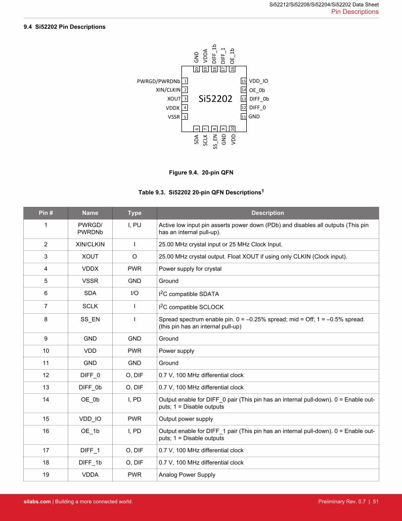
9.4 Si52202 Pin Descriptions
1
2
3
4
5
XOUTVDDX
PWRGD/PWRDNbXIN/CLKIN
6 7
SDA
SCLK
GND
VDD
8 9 10
15
14
13
12
11
20 19 18 17 16
GND
VDDA
DIFF
_1b
DIFF
_1
VDD_IO
DIFF_0bDIFF_0
OE_0b
GND
Si52202
VSSR
SS_E
N
OE_
1b
Figure 9.4. 20-pin QFN
Table 9.3. Si52202 20-pin QFN Descriptions1
Pin # Name Type Description
1 PWRGD/PWRDNb
I, PU Active low input pin asserts power down (PDb) and disables all outputs (This pinhas an internal pull-up).
2 XIN/CLKIN I 25.00 MHz crystal input or 25 MHz Clock Input.
3 XOUT O 25.00 MHz crystal output. Float XOUT if using only CLKIN (Clock input).
4 VDDX PWR Power supply for crystal
5 VSSR GND Ground
6 SDA I/O I2C compatible SDATA
7 SCLK I I2C compatible SCLOCK
8 SS_EN I Spread spectrum enable pin. 0 = –0.25% spread; mid = Off; 1 = –0.5% spread.(this pin has an internal pull-up)
9 GND GND Ground
10 VDD PWR Power supply
11 GND GND Ground
12 DIFF_0 O, DIF 0.7 V, 100 MHz differential clock
13 DIFF_0b O, DIF 0.7 V, 100 MHz differential clock
14 OE_0b I, PD Output enable for DIFF_0 pair (This pin has an internal pull-down). 0 = Enable out-puts; 1 = Disable outputs
15 VDD_IO PWR Output power supply
16 OE_1b I, PD Output enable for DIFF_1 pair (This pin has an internal pull-down). 0 = Enable out-puts; 1 = Disable outputs
17 DIFF_1 O, DIF 0.7 V, 100 MHz differential clock
18 DIFF_1b O, DIF 0.7 V, 100 MHz differential clock
19 VDDA PWR Analog Power Supply
Si52212/Si52208/Si52204/Si52202 Data SheetPin Descriptions
silabs.com | Building a more connected world. Preliminary Rev. 0.7 | 51

Pin # Name Type Description
20 GND GND Ground
GND PAD GND Ground pad. This pad provides an electrical and thermal connection to ground andmust be connected for proper operation. Use as many vias as practical, and keepthe via length to an internal ground plane as short as possible.
Note:1. Contact factory for 133/200M output frequencies.
Si52212/Si52208/Si52204/Si52202 Data SheetPin Descriptions
silabs.com | Building a more connected world. Preliminary Rev. 0.7 | 52

10. Packaging
10.1 Si52212 Package
The figure below illustrates the package details for the Si52212 in a 64-Lead 9 x 9 mm QFN package. The table lists the values for thedimensions shown in the illustration.
Figure 10.1. 64L 9 x 9 mm QFN Package Diagram
Table 10.1. Package Diagram Dimensions
Dimension Min Nom Max
A 0.80 0.85 0.90
A1 0.00 0.02 0.05
b 0.18 0.25 0.30
D 9.00 BSC
D2 5.10 5.20 5.30
e 0.50 BSC
E 9.00 BSC
E2 5.10 5.20 5.30
L 0.30 0.40 0.50
aaa 0.15
bbb 0.10
ccc 0.08
ddd 0.10
eee 0.05
Si52212/Si52208/Si52204/Si52202 Data SheetPackaging
silabs.com | Building a more connected world. Preliminary Rev. 0.7 | 53

Dimension Min Nom Max
Note:1. All dimensions shown are in millimeters (mm) unless otherwise noted.2. Dimensioning and Tolerancing per ANSI Y14.5M-1994.3. This drawing conforms to JEDEC Outline MO-220.4. Recommended card reflow profile is per JEDEC/IPC J-STD-020D specification for Small Body Components.
10.2 Si52212 Land Pattern
The following figure illustrates the land pattern details for the Si52212 in a 64-Lead 9 x 9 mm QFN package. The table lists the valuesfor the dimensions shown in the illustration.
Figure 10.2. 64L 9 x 9 mm QFN Land Pattern
Si52212/Si52208/Si52204/Si52202 Data SheetPackaging
silabs.com | Building a more connected world. Preliminary Rev. 0.7 | 54
Table 10.2. PCB Land Pattern Dimensions
Dimension mm
C1 8.90
C2 8.90
E 0.50
X1 0.30
Y1 0.85
X2 5.30
Y2 5.30
Notes:
General1. All dimensions shown are in millimeters (mm).2. This Land Pattern Design is based on the IPC-7351 guidelines.3. All dimensions shown are at Maximum Material Condition (MMC). Least Material Condition (LMC) is calculated based on a Fabri-
cation Allowance of 0.05 mm.
Solder Mask Design1. All metal pads are to be non-solder mask defined (NSMD). Clearance between the solder mask and the metal pad is to be 60 mm
minimum, all the way around the pad.
Stencil Design1. A stainless steel, laser-cut and electro-polished stencil with trapezoidal walls should be used to assure good solder paste release.2. The stencil thickness should be 0.125 mm (5 mils).3. The ratio of stencil aperture to land pad size should be 1:1 for all pads.4. A 3x3 array of 1.25 mm square openings on a 1.80 mm pitch should be used for the center ground pad.
Card Assembly1. A No-Clean, Type-3 solder paste is recommended.2. The recommended card reflow profile is per the JEDEC/IPC J-STD-020 specification for Small Body Components.
Si52212/Si52208/Si52204/Si52202 Data SheetPackaging
silabs.com | Building a more connected world. Preliminary Rev. 0.7 | 55

10.3 Si52208 Package
The figure below illustrates the package details for the Si52208 in a 48-Lead 6 x 6 mm QFN package. The table lists the values for thedimensions shown in the illustration.
Figure 10.3. 48L 6 x 6 mm QFN Package Diagram
Table 10.3. Package Diagram Dimensions
Dimension Min Nom Max
A 0.80 0.85 0.90
A1 0.00 0.02 0.05
b 0.15 0.20 0.25
D 6.00 BSC
D2 3.5 3.6 3.7
e 0.40 BSC
E 6.00 BSC
E2 3.5 3.6 3.7
L 0.30 0.40 0.50
aaa 0.10
bbb 0.10
ccc 0.10
ddd 0.05
eee 0.08
Si52212/Si52208/Si52204/Si52202 Data SheetPackaging
silabs.com | Building a more connected world. Preliminary Rev. 0.7 | 56

Dimension Min Nom Max
Note:1. All dimensions shown are in millimeters (mm) unless otherwise noted.2. Dimensioning and Tolerancing per ANSI Y14.5M-1994.3. This drawing conforms to JEDEC Outline MO-220.4. Recommended card reflow profile is per JEDEC/IPC J-STD-020 specification for Small Body Components.
10.4 Si52208 Land Pattern
The figure below illustrates the land pattern details for the Si52208 in a 48-Lead, 6 x 6 mm QFN package. The table lists the values forthe dimensions shown in the illustration.
Figure 10.4. 48L 6 x 6 mm QFN Land Pattern
Si52212/Si52208/Si52204/Si52202 Data SheetPackaging
silabs.com | Building a more connected world. Preliminary Rev. 0.7 | 57

Table 10.4. PCB Land Pattern Dimensions
Dimension mm
C1 5.90
C2 5.90
X1 0.20
X2 3.60
Y1 0.85
Y2 3.60
e 0.40 BSC
Notes:
General1. All dimensions shown are in millimeters (mm) unless otherwise noted.2. Dimensioning and Tolerancing is per the ANSI Y14.5M-1994 specification.3. This Land Pattern Design is based on IPC-7351 guidelines.4. All dimensions shown are at Maximum Material Condition (MMC). Least Material Condition (LMC) is calculated based on a Fabri-
cation Allowance of 0.05 mm.
Solder Mask Design1. All metal pads are to be non-solder mask defined (NSMD). Clearance between the solder mask and the metal pad is to be 60 mm
minimum, all the way around the pad.
Stencil Design1. A stainless steel, laser-cut and electro-polished stencil with trapezoidal walls should be used to assure good solder paste release.2. The stencil thickness should be 0.125 mm (5 mils).3. The ratio of stencil aperture to land pad size should be 1:1 for the perimeter pads.4. A 3x3 array of 0.90 mm square openings on 1.15mm pitch should be used for the center ground pad.
Card Assembly1. A No-Clean, Type-3 solder paste is recommended.2. The recommended card reflow profile is per the JEDEC/IPC J-STD-020 specification for Small Body Components.
Si52212/Si52208/Si52204/Si52202 Data SheetPackaging
silabs.com | Building a more connected world. Preliminary Rev. 0.7 | 58

10.5 Si52204 Package
The figure below illustrates the package details for the Si52204 in a 32-Lead, 5 x 5 mm QFN package. The table lists the values for thedimensions shown in the illustration.
Figure 10.5. 32L 5 x 5 mm QFN Package Diagram
Si52212/Si52208/Si52204/Si52202 Data SheetPackaging
silabs.com | Building a more connected world. Preliminary Rev. 0.7 | 59

Table 10.5. Package Diagram Dimensions
Dimension Min Nom Max
A 0.80 0.85 0.90
A1 0.00 0.02 0.05
A3 0.20 REF
b 0.18 0.25 0.30
D/E 4.90 5.00 5.10
D2/E2 3.40 3.50 3.60
E 0.50 BSC
K 0.20 — —
L 0.30 0.40 0.50
R 0.09 — 0.14
aaa 0.15
bbb 0.10
ccc 0.10
ddd 0.05
eee 0.08
fff 0.10
Note:1. All dimensions shown are in millimeters (mm) unless otherwise noted.2. Dimensioning and Tolerancing per ANSI Y14.5M-1994.3. This drawing conforms to the JEDEC Solid State Outline MO-220, Variation VKKD-4.4. Recommended card reflow profile is per JEDEC/IPC J-STD-020 specification for Small Body Components.
Si52212/Si52208/Si52204/Si52202 Data SheetPackaging
silabs.com | Building a more connected world. Preliminary Rev. 0.7 | 60

10.6 Si52204 Land Pattern
The figure below illustrates the land pattern details for the Si52204 in a 32-Lead, 5 x 5 mm QFN package. The table lists the values forthe dimensions shown in the illustration.
Figure 10.6. 32L 5 x 5 mm QFN Land Pattern
Table 10.6. PCB Land Pattern Dimensions
Dimension mm
S1 4.01
S 4.01
L1 3.50
W1 3.50
e 0.50
W 0.26
L 0.86
Notes:
General1. All dimensions shown are in millimeters (mm) unless otherwise noted.2. This Land Pattern Design is based on IPC-7351 guidelines.
Solder Mask Design1. All metal pads are to be non-solder mask defined (NSMD). Clearance between the solder mask and the metal pad is to be 60 mm
minimum, all the way around the pad.
Stencil Design1. A stainless steel, laser-cut and electro-polished stencil with trapezoidal walls should be used to assure good solder paste release.2. The stencil thickness should be 0.125mm (5 mils).3. The ratio of stencil aperture to land pad size can be 1:1 for all perimeter pads.4. A 3x3 array of 0.85 mm square openings on 1.00 mm pitch can be used for the center ground pad.
Card Assembly1. A No-Clean, Type-3 solder paste is recommended.2. The recommended card reflow profile is per the JEDEC/IPC J-STD-020 specification for Small Body Components.
Si52212/Si52208/Si52204/Si52202 Data SheetPackaging
silabs.com | Building a more connected world. Preliminary Rev. 0.7 | 61

10.7 Si52202 Package
The figure below illustrates the package details for the Si52202 in a 20-Lead, 3 x 3 mm QFN package. The table lists the values for thedimensions shown in the illustration.
Figure 10.7. 20L 3 x 3 mm QFN Package Diagram
Si52212/Si52208/Si52204/Si52202 Data SheetPackaging
silabs.com | Building a more connected world. Preliminary Rev. 0.7 | 62

Table 10.7. Package Diagram Dimensions
Dimension Min Nom Max
A 0.80 0.85 0.90
A1 0.00 0.02 0.05
A3 — 0.65 —
A3 0.20 REF
b 0.15 0.20 0.25
D 3.00 BSC
D2 1.8 1.9 2.0
E 3.00 BSC
E2 1.8 1.9 2.0
e 0.40 BSC
K 0.20 — —
L 0.20 0.30 0.40
R 0.075 — 0.125
aaa 0.10
bbb 0.07
ccc 0.10
ddd 0.05
eee 0.08
fff 0.10
Note:1. All dimensions shown are in millimeters (mm) unless otherwise noted.2. Dimensioning and Tolerancing per ANSI Y14.5M-1994.3. The drawing complies with JEDEC MO-220.4. Recommended card reflow profile is per the JEDEC/IPC J-STD-020 specification for Small Body Components.
Si52212/Si52208/Si52204/Si52202 Data SheetPackaging
silabs.com | Building a more connected world. Preliminary Rev. 0.7 | 63

10.8 Si52202 Land Pattern
The figure below illustrates the land pattern details for the Si52202 in a 20-Lead, 3 x 3 mm QFN package. The table lists the values forthe dimensions shown in the illustration.
Figure 10.8. 20L 3 x 3 mm QFN Land Pattern
Si52212/Si52208/Si52204/Si52202 Data SheetPackaging
silabs.com | Building a more connected world. Preliminary Rev. 0.7 | 64

Table 10.8. PCB Land Pattern Dimensions
Dimension mm
C1 3.10
C2 3.10
X1 0.20
X2 1.90
Y1 0.70
Y2 1.90
e 0.40 BSC
Notes:
General1. All dimensions shown are in millimeters (mm) unless otherwise noted.2. Dimensioning and Tolerancing is per the ANSI Y14.5M-1994 specification.3. This Land Pattern Design is based on IPC-7351 guidelines.4. All dimensions shown are at Maximum Material Condition (MMC). Least Material Condition (LMC) is calculated based on a Fabri-
cation Allowance of 0.05 mm.
Solder Mask Design1. All metal pads are to be non-solder mask defined (NSMD). Clearance between the solder mask and the metal pad is to be 60 µm
minimum, all the way around the pad.
Stencil Design1. A stainless steel, laser-cut and electro-polished stencil with trapezoidal walls should be used to assure good solder paste release.2. The stencil thickness should be 0.125 mm (5 mils).3. The ratio of stencil aperture to land pad size should be 1:1 for the perimeter pads.4. A 3x3 array of 0.90 mm square openings on 1.15 mm pitch should be used for the center ground pad.
Card Assembly1. A No-Clean, Type-3 solder paste is recommended.2. The recommended card reflow profile is per the JEDEC/IPC J-STD-020 specification for Small Body Components.
Si52212/Si52208/Si52204/Si52202 Data SheetPackaging
silabs.com | Building a more connected world. Preliminary Rev. 0.7 | 65

10.9 Si52212 Top Markings
Figure 10.9. Si52212 Top Marking
Table 10.9. Si52212 Top Marking Explanation
Line Characters Description
1 52212 Device part number
2 A01A Device part number
3 YYWWTTTTTT YY = Assembly year
WW = Assembly work weekTTTTTT = Manufacturing trace code
4 e# CC e# = Lead-finish symbol. # is a number
CC = Country of origin (ISO abbreviation)
Si52212/Si52208/Si52204/Si52202 Data SheetPackaging
silabs.com | Building a more connected world. Preliminary Rev. 0.7 | 66

10.10 Si52208 Top Markings
Figure 10.10. Si52208 Top Marking
Table 10.10. Si52208 Top Marking Explanation
Line Characters Description
1 52208 Device part number
2 A01A Device part number
3 TTTTTT TTTTTT = Manufacturing trace code
4 YYWW YY = Assembly year
WW = Assembly work week
Si52212/Si52208/Si52204/Si52202 Data SheetPackaging
silabs.com | Building a more connected world. Preliminary Rev. 0.7 | 67

10.11 Si52204 Top Markings
Figure 10.11. Si52204 Top Marking
Table 10.11. Si52204 Top Marking Explanation
Line Characters Description
1 52204 Device part number
2 A01A Device part number
3 TTTTTT TTTTTT = Manufacturing trace code
4 YYWW YY = Assembly year
WW = Assembly work week
Si52212/Si52208/Si52204/Si52202 Data SheetPackaging
silabs.com | Building a more connected world. Preliminary Rev. 0.7 | 68
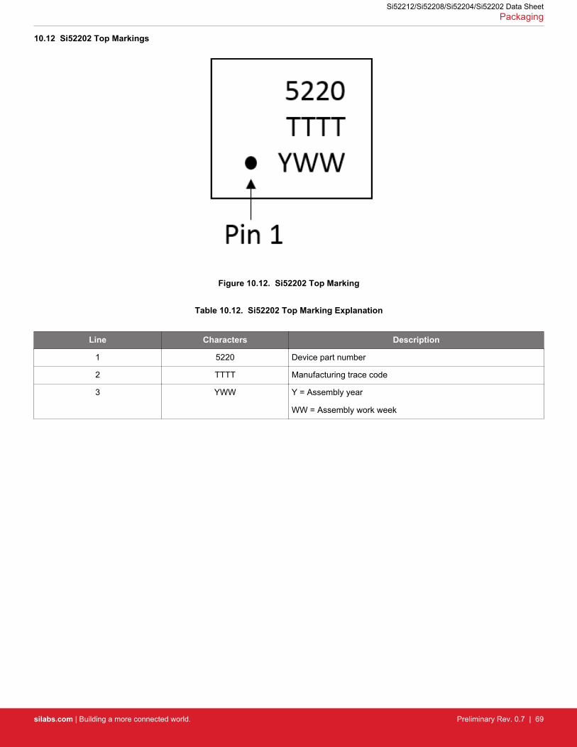
10.12 Si52202 Top Markings
Figure 10.12. Si52202 Top Marking
Table 10.12. Si52202 Top Marking Explanation
Line Characters Description
1 5220 Device part number
2 TTTT Manufacturing trace code
3 YWW Y = Assembly year
WW = Assembly work week
Si52212/Si52208/Si52204/Si52202 Data SheetPackaging
silabs.com | Building a more connected world. Preliminary Rev. 0.7 | 69
11. Revision History
11.1 Revision 0.7
September 20, 2017• Initial Release.
Si52212/Si52208/Si52204/Si52202 Data SheetRevision History
silabs.com | Building a more connected world. Preliminary Rev. 0.7 | 70

http://www.silabs.com
Silicon Laboratories Inc.400 West Cesar ChavezAustin, TX 78701USA
ClockBuilder ProOne-click access to Timing tools, documentation, software, source code libraries & more. Available for Windows and iOS (CBGo only).
www.silabs.com/CBPro
Timing Portfoliowww.silabs.com/timing
SW/HWwww.silabs.com/CBPro
Qualitywww.silabs.com/quality
Support and Communitycommunity.silabs.com
DisclaimerSilicon Labs intends to provide customers with the latest, accurate, and in-depth documentation of all peripherals and modules available for system and software implementers using or intending to use the Silicon Labs products. Characterization data, available modules and peripherals, memory sizes and memory addresses refer to each specific device, and "Typical" parameters provided can and do vary in different applications. Application examples described herein are for illustrative purposes only. Silicon Labs reserves the right to make changes without further notice and limitation to product information, specifications, and descriptions herein, and does not give warranties as to the accuracy or completeness of the included information. Silicon Labs shall have no liability for the consequences of use of the information supplied herein. This document does not imply or express copyright licenses granted hereunder to design or fabricate any integrated circuits. The products are not designed or authorized to be used within any Life Support System without the specific written consent of Silicon Labs. A "Life Support System" is any product or system intended to support or sustain life and/or health, which, if it fails, can be reasonably expected to result in significant personal injury or death. Silicon Labs products are not designed or authorized for military applications. Silicon Labs products shall under no circumstances be used in weapons of mass destruction including (but not limited to) nuclear, biological or chemical weapons, or missiles capable of delivering such weapons.
Trademark InformationSilicon Laboratories Inc.® , Silicon Laboratories®, Silicon Labs®, SiLabs® and the Silicon Labs logo®, Bluegiga®, Bluegiga Logo®, Clockbuilder®, CMEMS®, DSPLL®, EFM®, EFM32®, EFR, Ember®, Energy Micro, Energy Micro logo and combinations thereof, "the world’s most energy friendly microcontrollers", Ember®, EZLink®, EZRadio®, EZRadioPRO®, Gecko®, ISOmodem®, Micrium, Precision32®, ProSLIC®, Simplicity Studio®, SiPHY®, Telegesis, the Telegesis Logo®, USBXpress®, Zentri and others are trademarks or registered trademarks of Silicon Labs. ARM, CORTEX, Cortex-M3 and THUMB are trademarks or registered trademarks of ARM Holdings. Keil is a registered trademark of ARM Limited. All other products or brand names mentioned herein are trademarks of their respective holders.


![NATURAL SCIENCES D568/12 ADMISSIONS ASSESSMENT 40 … · Ω, 2 Ω, 4 Ω, 8 Ω, 16 Ω, 32 Ω, 64 Ω, … connected in parallel with the cell. ... [2 marks] Answer: ... is used as the](https://img.pdfslide.net/doc/110x75/5f2363f7b03d7e4ce06bc15b/natural-sciences-d56812-admissions-assessment-40-2-4-8-16-32.jpg)


![LABORATÓRIO DE SISTEMAS MECATRÔNICOS E ROBÓTICA ] - LAB.pdf · Resistores - 1,0 Ω - 100k Ω 1,2 Ω - 120k Ω 1,5 Ω - 150k Ω 1,8 Ω- 180k Ω 2,2 Ω– 220k Ω 2,7 Ω– 270k](https://img.pdfslide.net/doc/110x75/5c245c1a09d3f224508c4b48/laboratorio-de-sistemas-mecatronicos-e-robotica-labpdf-resistores-.jpg)