Embed Size (px)
Citation preview
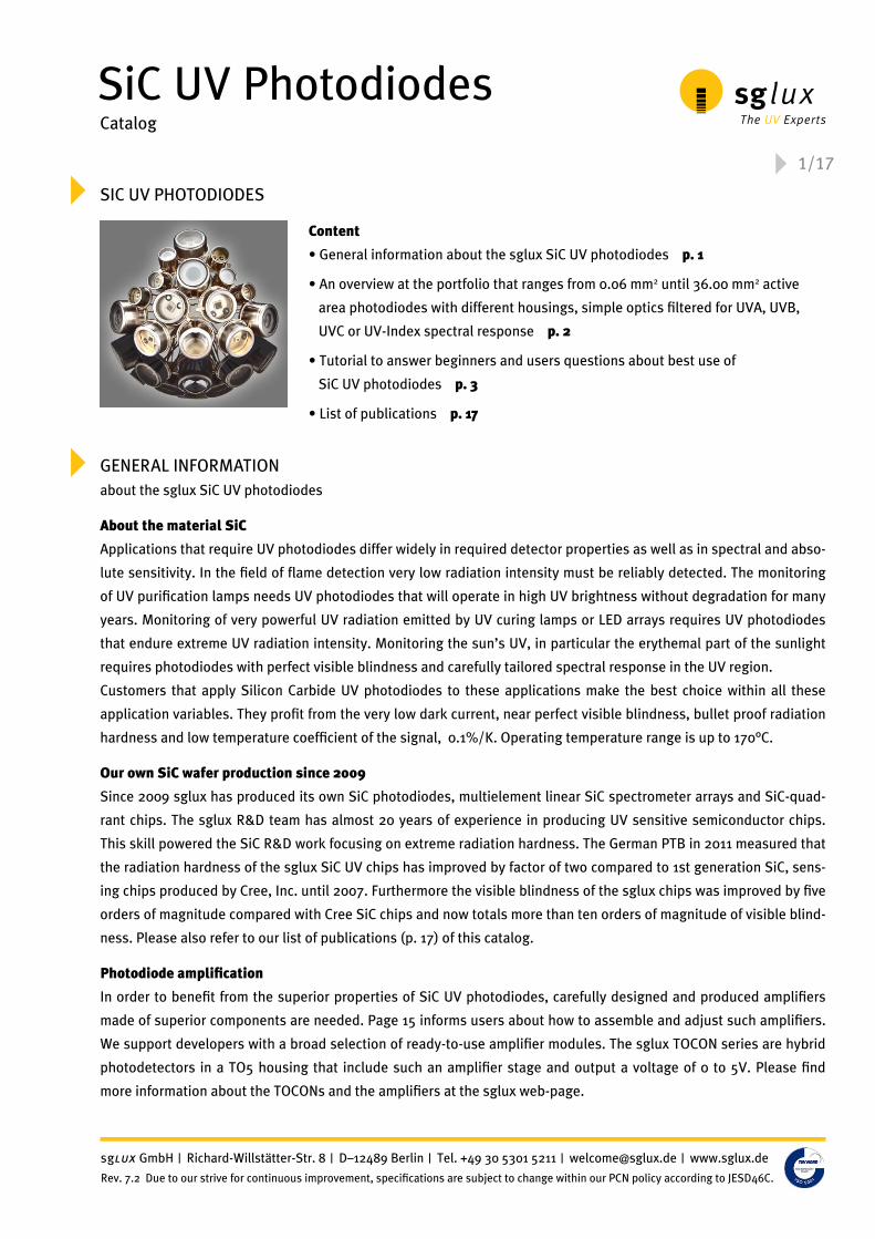
SiC UV photodiodeS
Content
• General information about the sglux SiC UV photodiodes p. 1
• An overview at the portfolio that ranges from 0.06 mm2 until 36.00 mm2 active
area photodiodes with different housings, simple optics filtered for UVA, UVB,
UVC or UV-Index spectral response p. 2
• Tutorial to answer beginners and users questions about best use of
SiC UV photodiodes p. 3
• List of publications p. 17
General information about the sglux SiC UV photodiodes
About the material SiC
Applications that require UV photodiodes differ widely in required detector properties as well as in spectral and abso-
lute sensitivity. In the field of flame detection very low radiation intensity must be reliably detected. The monitoring
of UV purification lamps needs UV photodiodes that will operate in high UV brightness without degradation for many
years. Monitoring of very powerful UV radiation emitted by UV curing lamps or LED arrays requires UV photodiodes
that endure extreme UV radiation intensity. Monitoring the sun’s UV, in particular the erythemal part of the sunlight
requires photodiodes with perfect visible blindness and carefully tailored spectral response in the UV region.
Customers that apply Silicon Carbide UV photodiodes to these applications make the best choice within all these
application variables. They profit from the very low dark current, near perfect visible blindness, bullet proof radiation
hardness and low temperature coefficient of the signal, 0.1%/K. Operating temperature range is up to 170°C.
Our own SiC wafer production since 2009
Since 2009 sglux has produced its own SiC photodiodes, multielement linear SiC spectrometer arrays and SiC-quad-
rant chips. The sglux R&D team has almost 20 years of experience in producing UV sensitive semiconductor chips.
This skill powered the SiC R&D work focusing on extreme radiation hardness. The German PTB in 2011 measured that
the radiation hardness of the sglux SiC UV chips has improved by factor of two compared to 1st generation SiC, sens-
ing chips produced by Cree, Inc. until 2007. Furthermore the visible blindness of the sglux chips was improved by five
orders of magnitude compared with Cree SiC chips and now totals more than ten orders of magnitude of visible blind-
ness. Please also refer to our list of publications (p. 17) of this catalog.
Photodiode amplification
In order to benefit from the superior properties of SiC UV photodiodes, carefully designed and produced amplifiers
made of superior components are needed. Page 15 informs users about how to assemble and adjust such amplifiers.
We support developers with a broad selection of ready-to-use amplifier modules. The sglux TOCON series are hybrid
photodetectors in a TO5 housing that include such an amplifier stage and output a voltage of 0 to 5V. Please find
more information about the TOCONs and the amplifiers at the sglux web-page.
SiC UV PhotodiodesCatalog
sglux GmbH | Richard-Willstätter-Str. 8 | D–12489 Berlin | Tel. +49 30 5301 5211 | [email protected] | www.sglux.de
Rev. 7.2 Due to our strive for continuous improvement, specifications are subject to change within our PCN policy according to JESD46C.
1/17
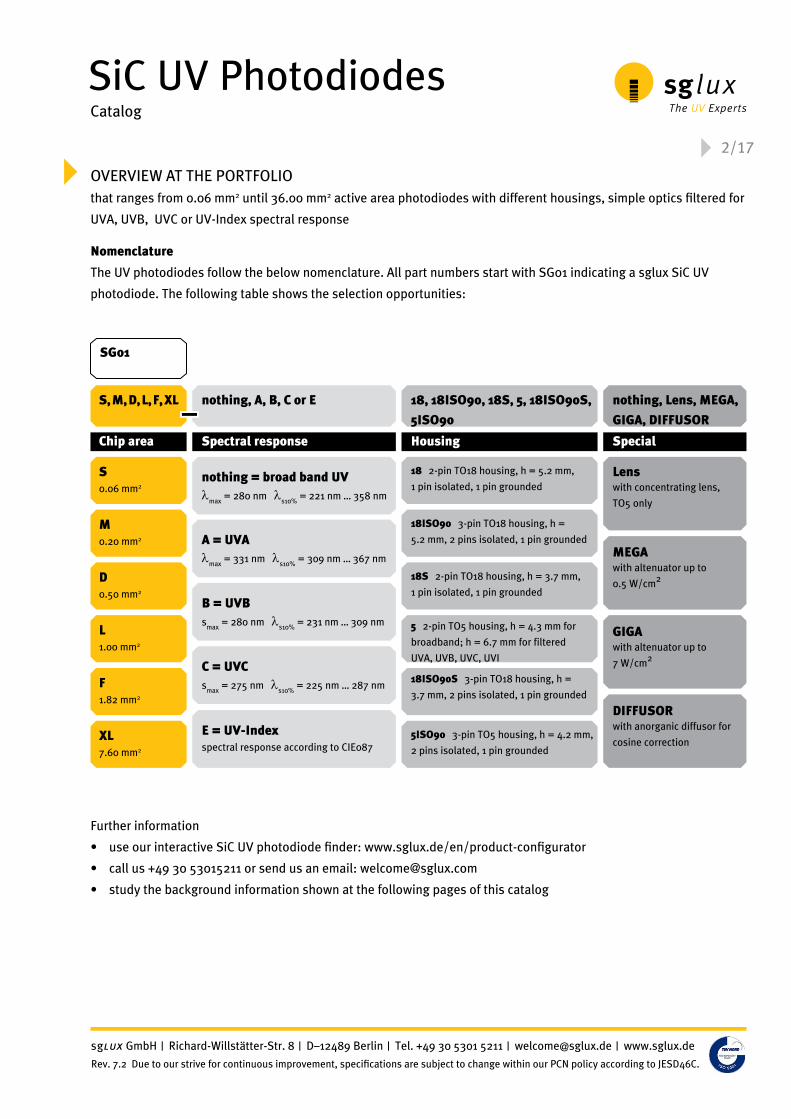
oVerView at the portfolio that ranges from 0.06 mm2 until 36.00 mm2 active area photodiodes with different housings, simple optics filtered for
UVA, UVB, UVC or UV-Index spectral response
Nomenclature
The UV photodiodes follow the below nomenclature. All part numbers start with SG01 indicating a sglux SiC UV
photodiode. The following table shows the selection opportunities:
Further information
• use our interactive SiC UV photodiode finder: www.sglux.de/en/product-configurator
• call us +49 30 53015211 or send us an email: [email protected]
• study the background information shown at the following pages of this catalog
SiC UV PhotodiodesCatalog
S0.06 mm2
M0.20 mm2
D0.50 mm2
F1.82 mm2
XL7.60 mm2
nothing = broad band UVλ
max = 280 nm λ
s10% = 221 nm … 358 nm
A = UVAλ
max = 331 nm λ
s10% = 309 nm … 367 nm
B = UVBs
max = 280 nm λ
s10% = 231 nm … 309 nm
E = UV-Indexspectral response according to CIE087
Lenswith concentrating lens,
TO5 only
MEGAwith altenuator up to
0.5 W/cm2
SG01
S, M, D, L, F, XL nothing, A, B, C or E 18, 18ISO90, 18S, 5, 18ISO90S,
5ISO90
nothing, Lens, MEGA,
GIGA, DIFFUSOR
18 2-pin TO18 housing, h = 5.2 mm,
1 pin isolated, 1 pin grounded
18ISO90 3-pin TO18 housing, h =
5.2 mm, 2 pins isolated, 1 pin grounded
18S 2-pin TO18 housing, h = 3.7 mm,
1 pin isolated, 1 pin grounded
18ISO90S 3-pin TO18 housing, h =
3.7 mm, 2 pins isolated, 1 pin grounded
5ISO90 3-pin TO5 housing, h = 4.2 mm,
2 pins isolated, 1 pin grounded
Chip area Spectral response Housing Special
L1.00 mm2
C = UVCs
max = 275 nm λ
s10% = 225 nm … 287 nm
5 2-pin TO5 housing, h = 4.3 mm for
broadband; h = 6.7 mm for filtered
UVA, UVB, UVC, UVI
GIGAwith altenuator up to
7 W/cm2
DIFFUSORwith anorganic diffusor for
cosine correction
2/17
sglux GmbH | Richard-Willstätter-Str. 8 | D–12489 Berlin | Tel. +49 30 5301 5211 | [email protected] | www.sglux.de
Rev. 7.2 Due to our strive for continuous improvement, specifications are subject to change within our PCN policy according to JESD46C.
tUtorial
to answer beginners and users questions about best use of SiC UV photodiodes
General information about the sglux SiC UV photodiodes
• About the material SiC p. 1
• sglux inhouse SiC wafer production since 2009 p. 1
• Photodiode amplification p. 1
Overview at the portfolio that ranges from 0.06 mm2 until 36.00 mm2 active area photodiodes
with different housings, simple optics filtered for UVA, UVB, UVC or UV-Index spectral response p. 2
• Nomenclature p. 2
Tutorial to answer beginners and users questions about best use of SiC UV photodiodes
1.0 Selection of the chip active area (photocurrent limits) p. 4
1.1 Problems with current too low p. 5
1.2 Problems with current too high p. 6
1.3 Calculation of the relation between UV radiation and photocurrent p. 7
2.0 Selection of the spectral response p. 9
2.1 Unfiltered SiC p. 10
2.2 Filtered SiC p. 11
3.0 Packaging features p. 12
3.1 Overview p. 12
3.2 Drawings p. 13
4.0 Special features p. 15
• Appendix A Photodiode amplification notes p. 15
• Upgrade to a TOCON or a PROBE p. 16
List of publications p. 17
SiC UV PhotodiodesCatalog
3/17
sglux GmbH | Richard-Willstätter-Str. 8 | D–12489 Berlin | Tel. +49 30 5301 5211 | [email protected] | www.sglux.de
Rev. 7.2 Due to our strive for continuous improvement, specifications are subject to change within our PCN policy according to JESD46C.
1.0 Selection of the chip active area (photocurrent limits)
The chip active area determines how many photons can be collected by a photodetector. Semiconductor detectors,
such as SiC UV photodiodes, convert photons into an electrical current, the photocurrent I. This photocurrent rises
linearly with the irradiation power and the chip active area. sglux produces seven different area sizes:
A1 = 0.06 mm2 (S-type)
A2 = 0.20 mm2 (M-type)
A3 = 0.50 mm2 (D-type)
A4 = 1.00 mm2 (L-type)
A5 = 1.82 mm2 (F-type)
A5 = 7.60 mm2 (XL-type)
A6 = 36 mm2 (XXL-type)
As the detector price rises with increasing active area, the area selection basically is a compromise between costs and
current.
If you know the minimum and maximum irradiance you like to measure with the UV photodiode the following
simplified formula (1) shows a rough estimation of the photocurrent I given a particular chip active area AChip
.
I = Achip
* Eλ * 1.000 (1)
where I is the photocurrent in nA, Achip
is the chip active area in mm2 (enter values of 0.06 or 0.2 or 0.5 or 1 or
1.82, 7.6 or 36) and Eλ is the spectral irradiance of the UV light source you like to measure in mWcm-2. You may find
more information about photocurrent calculation in chapter 1.3 (Calculation of the relation between UV radiation and
photocurrent), p. 7.
If you do not know the irradiance coming from your UV light source chapter 1. section 1.3 gives some examples of
common UV sources.
The minimum current (photodiode output at lowest irradiance to be measured) should not fall below 500pA. The
maximum current must not exceed 400mA if the component’s diode properties are to be maintained. Please refer to
a detailed discussion on suitable minimum and maximum currents in the following chapters 1. section 1.1 (Problems
with current too low) and 1. section 1.2 (Problems with current too high). These chapters assume a certain basic
knowledge in photodiode amplifier circuits. If you are not familiar with circuits please see Appendix A (Photodiode
Amplification Notes) at p. 15.
SiC UV PhotodiodesCatalog
4/17
sglux GmbH | Richard-Willstätter-Str. 8 | D–12489 Berlin | Tel. +49 30 5301 5211 | [email protected] | www.sglux.de
Rev. 7.2 Due to our strive for continuous improvement, specifications are subject to change within our PCN policy according to JESD46C.
1.1 Problems with current too low
If the current is too low, one ore more of the following problems (P1 – P
4) may affect the measurement:
P1 > The measurement signal comes too close to the UV photodiode dark current
P2 > High resistance feedback resistors (R
f) must be used which causes temperature drift and non linearity
problems
P3
> Speed problems
P4
> Risk of electromagnetic interferences
Using SiC, P1 can be neglected due to the extremely low dark current of the sglux 4H SiC UV photodiodes of only some
fA. P2 (temperature drift and non linearity) becomes essential from values R
f > 10 GW. Therefore, the photocurrent I
should be strong enough to allow Rf values of ≤ 10 GW. The relation between I and R
f is given by Ohm’s law:
I = Usupply
/ Rf
(2)
where Usupply
is the supply voltage of the used transimpedance amplifier. A typical value is 5.00 V. Formula (2)
calculates:
Imin
= 5.00V/10 GW = 500pA (3)
If a higher speed measurement is needed P3 (speed problems) could become an issue. As the SiC UV photodiode’s
detection speed is extremely high (in nanoseconds only) the amplifier speed (rise time) determines the circuit’s
speed. The amplifier rise time is calculated with the following formula:
t = Rf * C
f (4)
where Cf is the feedback capacitor value which should not be lower than 0.1 nF. A lower C
f risks hitting the circuit’s
resonance. Using a Cf = 0.1 nF and a R
f = 10 GW the rise time is calculated as follows:
t = 10 GW * 0.1 nF = 1 second (5)
Formula (5) shows that using a Rf = 10 GW the circuit becomes very slow. If a higher speed is needed the photocurrent
I must be increased to allow a decrease in the Rf
value. This can be done by increasing the UV radiation or, if that is
not feasible, by increasing the chip active area.
The last problem (P4) that can be caused with too low photocurrent (= due to too small an active area) is complications
from electromagnetic interferences. This is a general issue. Decreasing photocurrents call for increasing shielding
efforts which then increases the system price of the product. If the radiation (and thus the current) is low one should
consider using a sglux TOCON amplified hybrid UV sensor.
SiC UV PhotodiodesCatalog
5/17
sglux GmbH | Richard-Willstätter-Str. 8 | D–12489 Berlin | Tel. +49 30 5301 5211 | [email protected] | www.sglux.de
Rev. 7.2 Due to our strive for continuous improvement, specifications are subject to change within our PCN policy according to JESD46C.
Conclusion of needed minimum photocurrent Imin
To achieve a stable temperature and linear photodiode-amplifier system the lowest measurement current Imin
should
be higher than 500pA. If a high speed measuring circuit is needed Imin
is calculated by the following formula:
Imin
= Usupply
* Cf * t -1 (6)
With Usupply
= 5.00V (typical value), Cf = 0.1nF (recommended value) and R
f = 10 GW (lowest recommended value) the
formula reduces to:
Imin
= 500 * t -1 (7)
where Imin
results in nanoamperes (nA) and t must be in milliseconds.
In general, given these reasons, a decreasing photocurrent needs a more advanced amplifier design and better shield-
ing. If you are not familiar with low current circuit development you should consider selecting a higher current (and
thus larger active area) photodiode even if the price of a photodiode is higher. This strategy will provide conservative
results and the initial increased financial cost will save you money in the long run.
1.2 Problems with current too high
In the previous pages we discussed the calculation of a minimum recommended photodiode current. It also should be
mentioned that aside from the photocurrent being too low too high of a current may cause problems as well due to
saturation effects. The saturation current Isat
of a photodiode is the current limit from which the output of a photodi-
ode turns to arbitrary values. It is determined by the photodiode’s open circuit voltage VOC
and its serial resistance RS
following the formula below:
Isat
= VOC
/ RS (8)
A typical value (SiC photodiode) for VOC
is 2.0V and for RS = 5W. The calculation is a follows:
Isat
= 2.0 V / 5 W = 400mA.
The needed minimum current (500 pA) is higher than the saturation current is higher by six orders of magnitude.
Reaching the saturation limit of a SiC photodiode is therefore very unlikely.
SiC UV PhotodiodesCatalog
6/17
sglux GmbH | Richard-Willstätter-Str. 8 | D–12489 Berlin | Tel. +49 30 5301 5211 | [email protected] | www.sglux.de
Rev. 7.2 Due to our strive for continuous improvement, specifications are subject to change within our PCN policy according to JESD46C.
1.3 Calculation of the relation between UV radiation and photocurrent
The photocurrent I is calculated by the following formula:
I = ∫ Achip
* Schip
(λ) * Esource
(λ)d λ (9)
where I is the photocurrent in A, Achip
is the chip active area in m2. Schip
is the chip’s spectral sensitivity in AW-1 and Eλ
is the spectral irradiance of the UV light source in Wm-2. Due to extreme visible and IR blindness (13 orders of magni-
tude) the integral value from 400nm to ∞ can be neglected even if Esource
(λ) is very strong. To get a rough estimate of
the photocurrent generated by a certain irradiance a simplification of (9) leads to (10). That simplification assumes
that the chip’s spectral sensitivity S and the UV source’s irradiance E is a constant value and does not depend on
wavelength. The calculation is:
I = Achip
* Schip
* Eλ * 10.000 (10)
where I is the photocurrent in nA, Achip
is the chip active area in mm2. Schip
is the chip’s spectral sensitivity in AW-1 and
Eλ is the spectral irradiance of the UV light source in mWcm-2.
A typical value of Schip
is 0.1 A/W. For further refinement please refer to the spectral response graph of the UV photo-
diode you are interested in (see Datasheet) or have a look at chapter 2.0 (Selection of the spectral response, p. 9) of
this guide.
If you know the spectral irradiance range, (minimal and maximal values), of the UV light source and you would like to
measure you can easily estimate the photocurrent I by using formula (10) and hence select a chip active area (S-, M-,
D-, L-, F-, XL- or XXL-type) that guarantees that your minimum radiation generates a photocurrent of more than 500
pA. The following table lists some common UV applications / light sources with their spectral irradiances at peak.
Please note that some simplifications apply; thus the table gives a rough estimation of photocurrents for the different
UV source types and different chip active areas.
SiC UV PhotodiodesCatalog
400nm
200 nm
7/17
sglux GmbH | Richard-Willstätter-Str. 8 | D–12489 Berlin | Tel. +49 30 5301 5211 | [email protected] | www.sglux.de
Rev. 7.2 Due to our strive for continuous improvement, specifications are subject to change within our PCN policy according to JESD46C.
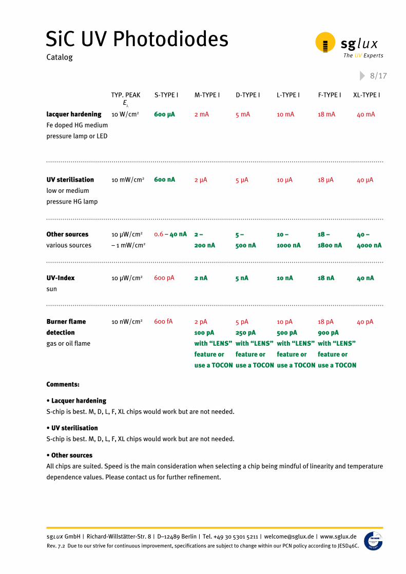
lacquer hardening
Fe doped HG medium
pressure lamp or LED
UV sterilisation
low or medium
pressure HG lamp
Other sources
various sources
UV-Index
sun
Burner flame
detection
gas or oil flame
10 W/cm2
10 mW/cm2
10 µW/cm2
– 1 mW/cm2
10 µW/cm2
10 nW/cm2
600 µA
600 nA
0.6 – 40 nA
600 pA
600 fA
2 mA
2 µA
2 –
200 nA
2 nA
2 pA
100 pA
with “LENS”
feature or
use a TOCON
typ. peakEλ
S-type i m-type i
SiC UV PhotodiodesCatalog
5 mA
5 µA
5 –
500 nA
5 nA
5 pA
250 pA
with “LENS”
feature or
use a TOCON
d-type i
10 mA
10 µA
10 –
1000 nA
10 nA
10 pA
500 pA
with “LENS”
feature or
use a TOCON
l-type i
18 mA
18 µA
18 –
1800 nA
18 nA
18 pA
900 pA
with “LENS”
feature or
use a TOCON
f-type i
40 mA
40 µA
40 –
4000 nA
40 nA
40 pA
Xl-type i
Comments:
• Lacquer hardening
S-chip is best. M, D, L, F, XL chips would work but are not needed.
• UV sterilisation
S-chip is best. M, D, L, F, XL chips would work but are not needed.
• Other sources
All chips are suited. Speed is the main consideration when selecting a chip being mindful of linearity and temperature
dependence values. Please contact us for further refinement.
8/17
sglux GmbH | Richard-Willstätter-Str. 8 | D–12489 Berlin | Tel. +49 30 5301 5211 | [email protected] | www.sglux.de
Rev. 7.2 Due to our strive for continuous improvement, specifications are subject to change within our PCN policy according to JESD46C.
• UV-Index
S-Chips are too small for this application. All other chips can be applied. The reliability increases with increasing chip
active area. Due to very low current the use of a TOCON (amplified hybrid sensor) should be considered.
• Burner flame detection
All chips are too small for this type of detection. A burner flame can be detected with the photodiode „SG01M-5Lens“
or “SG01D-5Lens” or “SG01L-5Lens” or “SG01F-5Lens”. This sensor works with a concentrating lens. Alternatively
the photodiode “SG01F-5ISO90” (1.82 mm2 active area) can be applied. However, this photodiode needs an external
concentrator lens. Please refer to chapter 4.0. (Special features), for more information. Another approach is to use a
sglux TOCON_ABC1 sensor with its included amplifier. The TOCON_ABC1 converts 0-18 nW/cm2 radiation into a 0-5 V
output voltage.
SiC UV PhotodiodesCatalog
9/17
sglux GmbH | Richard-Willstätter-Str. 8 | D–12489 Berlin | Tel. +49 30 5301 5211 | [email protected] | www.sglux.de
Rev. 7.2 Due to our strive for continuous improvement, specifications are subject to change within our PCN policy according to JESD46C.
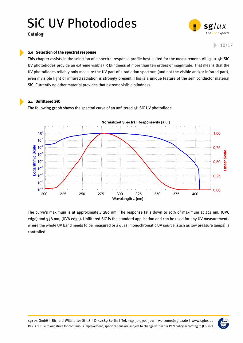
2.1 Unfiltered SiC
The following graph shows the spectral curve of an unfiltered 4H SiC UV photodiode.
The curve’s maximum is at approximately 280 nm. The response falls down to 10% of maximum at 221 nm, (UVC
edge) and 358 nm, (UVA edge). Unfiltered SiC is the standard application and can be used for any UV measurements
where the whole UV band needs to be measured or a quasi monochromatic UV source (such as low pressure lamps) is
controlled.
SiC UV PhotodiodesCatalog
10/172.0 Selection of the spectral response
This chapter assists in the selection of a spectral response profile best suited for the measurement. All sglux 4H SiC
UV photodiodes provide an extreme visible/IR blindness of more than ten orders of magnitude. That means that the
UV photodiodes reliably only measure the UV part of a radiation spectrum (and not the visible and/or infrared part),
even if visible light or infrared radiation is strongly present. This is a unique feature of the semiconductor material
SiC. Currently no other material provides that extreme visible blindness.
sglux GmbH | Richard-Willstätter-Str. 8 | D–12489 Berlin | Tel. +49 30 5301 5211 | [email protected] | www.sglux.de
Rev. 7.2 Due to our strive for continuous improvement, specifications are subject to change within our PCN policy according to JESD46C.
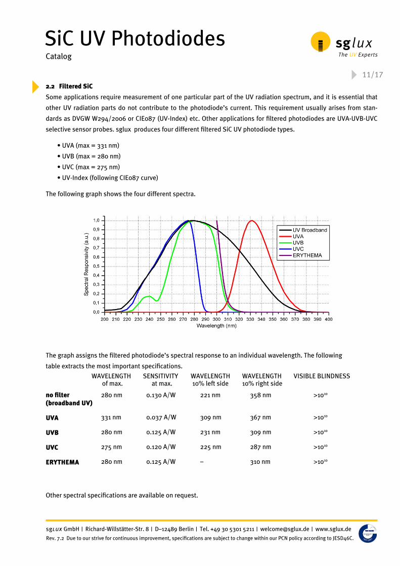
2.2 Filtered SiC
Some applications require measurement of one particular part of the UV radiation spectrum, and it is essential that
other UV radiation parts do not contribute to the photodiode’s current. This requirement usually arises from stan-
dards as DVGW W294/2006 or CIE087 (UV-Index) etc. Other applications for filtered photodiodes are UVA-UVB-UVC
selective sensor probes. sglux produces four different filtered SiC UV photodiode types.
• UVA (max = 331 nm)
• UVB (max = 280 nm)
• UVC (max = 275 nm)
• UV-Index (following CIE087 curve)
The following graph shows the four different spectra.
The graph assigns the filtered photodiode’s spectral response to an individual wavelength. The following
table extracts the most important specifications.
Other spectral specifications are available on request.
SiC UV PhotodiodesCatalog
no filter(broadband UV)
UVA
UVB
UVC
ERYTHEMA
280 nm
331 nm
280 nm
275 nm
280 nm
0.130 A/W
0.037 A/W
0.125 A/W
0.120 A/W
0.125 A/W
221 nm
309 nm
231 nm
225 nm
–
358 nm
367 nm
309 nm
287 nm
310 nm
>1010
>1010
>1010
>1010
>1010
waVelenGthof max.
SenSitiVityat max.
waVelenGth 10% left side
waVelenGth10% right side
ViSiBle BlindneSS
11/17
sglux GmbH | Richard-Willstätter-Str. 8 | D–12489 Berlin | Tel. +49 30 5301 5211 | [email protected] | www.sglux.de
Rev. 7.2 Due to our strive for continuous improvement, specifications are subject to change within our PCN policy according to JESD46C.
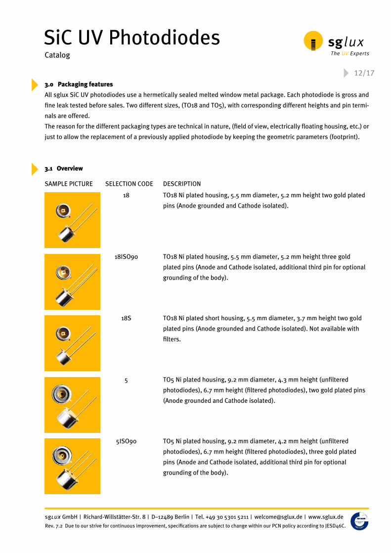
3.0 Packaging features
All sglux SiC UV photodiodes use a hermetically sealed melted window metal package. Each photodiode is gross and
fine leak tested before sales. Two different sizes, (TO18 and TO5), with corresponding different heights and pin termi-
nals are offered.
The reason for the different packaging types are technical in nature, (field of view, electrically floating housing, etc.) or
just to allow the replacement of a previously applied photodiode by keeping the geometric parameters (footprint).
3.1 Overview
SiC UV PhotodiodesCatalog
TO18 Ni plated housing, 5.5 mm diameter, 5.2 mm height two gold plated
pins (Anode grounded and Cathode isolated).
TO18 Ni plated housing, 5.5 mm diameter, 5.2 mm height three gold
plated pins (Anode and Cathode isolated, additional third pin for optional
grounding of the body).
TO18 Ni plated short housing, 5.5 mm diameter, 3.7 mm height two gold
plated pins (Anode grounded and Cathode isolated). Not available with
filters.
TO5 Ni plated housing, 9.2 mm diameter, 4.3 mm height (unfiltered
photodiodes), 6.7 mm height (filtered photodiodes), two gold plated pins
(Anode grounded and Cathode isolated).
TO5 Ni plated housing, 9.2 mm diameter, 4.2 mm height (unfiltered
photodiodes), 6.7 mm height (filtered photodiodes), three gold plated
pins (Anode and Cathode isolated, additional third pin for optional
grounding of the body).
18
18ISO90
18S
5
5ISO90
SeleCtion Code deSCriptionSample piCtUre
12/17
sglux GmbH | Richard-Willstätter-Str. 8 | D–12489 Berlin | Tel. +49 30 5301 5211 | [email protected] | www.sglux.de
Rev. 7.2 Due to our strive for continuous improvement, specifications are subject to change within our PCN policy according to JESD46C.
3.2 Drawings
Selection code “18” > TO18 Ni plated housing, 5.5 mm diameter, 5.2 mm height two gold plated pins
(Anode grounded and Cathode isolated).
Selection code “18ISO90” > TO18 Ni plated housing, 5.5 mm diameter, 5.2 mm height three gold plated pins
(Anode and Cathode isolated, additional third pin for optional grounding of the body).
Selection code “18S” > TO18 Ni plated short housing, 5.5 mm diameter, 3.7 mm height two gold plated pins
(Anode grounded and Cathode isolated). Not available with filters.
SiC UV PhotodiodesCatalog
13,5
05,
2
side view
chipposition
45°
11
45°
Ø0,45
3.35
bottom view
Ø2,54
Ø4,7
Ø3,9
top view
1Ø4,7
Ø3,9 1
Ø5,5
Ø5,5Ø5,5
chipposition50µmGND (case pin)
Anode
Cathode
13/17
sglux GmbH | Richard-Willstätter-Str. 8 | D–12489 Berlin | Tel. +49 30 5301 5211 | [email protected] | www.sglux.de
Rev. 7.2 Due to our strive for continuous improvement, specifications are subject to change within our PCN policy according to JESD46C.
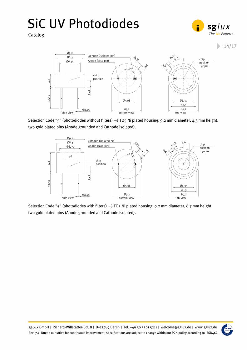
Selection Code ”5” (photodiodes without filters) > TO5 Ni plated housing, 9.2 mm diameter, 4.3 mm height,
two gold plated pins (Anode grounded and Cathode isolated).
Selection Code ”5” (photodiodes with filters) > TO5 Ni plated housing, 9.2 mm diameter, 6.7 mm height,
two gold plated pins (Anode grounded and Cathode isolated).
SiC UV PhotodiodesCatalog
14/17
sglux GmbH | Richard-Willstätter-Str. 8 | D–12489 Berlin | Tel. +49 30 5301 5211 | [email protected] | www.sglux.de
Rev. 7.2 Due to our strive for continuous improvement, specifications are subject to change within our PCN policy according to JESD46C.
4.0 Special features
Besides the three main selection criteria chip active area, spectral response and packaging details some special fea-
tures can be added to the photodiode’s properties. These special features are useful if the UV radiation is extremely
high or low or if a cosine FOV is needed. The below table shows the selectable special features.
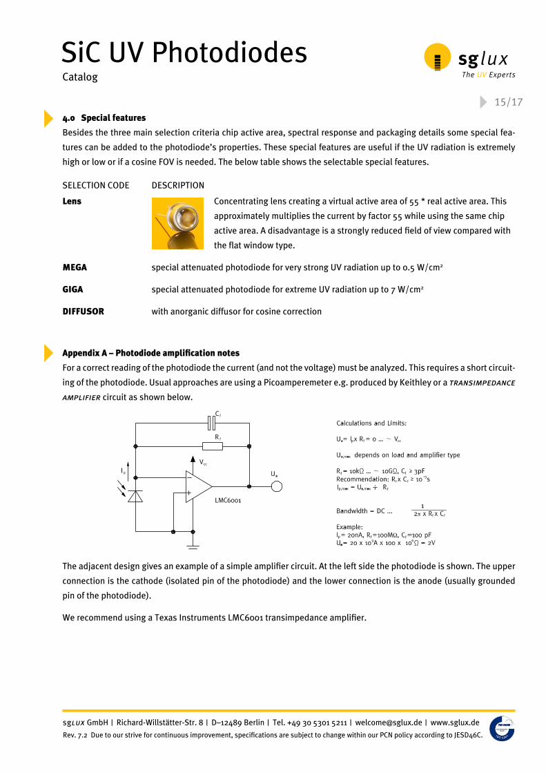
Appendix A – Photodiode amplification notes
For a correct reading of the photodiode the current (and not the voltage) must be analyzed. This requires a short circuit-
ing of the photodiode. Usual approaches are using a Picoamperemeter e.g. produced by Keithley or a transimpedance
amplifier circuit as shown below.
The adjacent design gives an example of a simple amplifier circuit. At the left side the photodiode is shown. The upper
connection is the cathode (isolated pin of the photodiode) and the lower connection is the anode (usually grounded
pin of the photodiode).
We recommend using a Texas Instruments LMC6001 transimpedance amplifier.
SiC UV PhotodiodesCatalog
Concentrating lens creating a virtual active area of 55 * real active area. This
approximately multiplies the current by factor 55 while using the same chip
active area. A disadvantage is a strongly reduced field of view compared with
the flat window type.
special attenuated photodiode for very strong UV radiation up to 0.5 W/cm2
special attenuated photodiode for extreme UV radiation up to 7 W/cm2
with anorganic diffusor for cosine correction
SeleCtion Code deSCription
Lens
MEGA
GIGA
DIFFUSOR
15/17
sglux GmbH | Richard-Willstätter-Str. 8 | D–12489 Berlin | Tel. +49 30 5301 5211 | [email protected] | www.sglux.de
Rev. 7.2 Due to our strive for continuous improvement, specifications are subject to change within our PCN policy according to JESD46C.
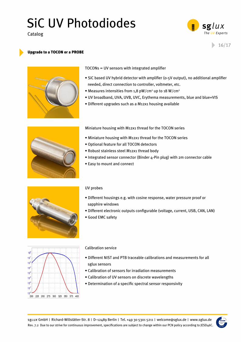
Upgrade to a TOCON or a PROBE
TOCONs = UV sensors with integrated amplifier
• SiC based UV hybrid detector with amplifier (0-5V output), no additional amplifier
needed, direct connection to controller, voltmeter, etc.
• Measures intensities from 1,8 pW/cm2 up to 18 W/cm2
• UV broadband, UVA, UVB, UVC, Erythema measurements, blue and blue+VIS
• Different upgrades such as a M12x1 housing available
Miniature housing with M12x1 thread for the TOCON series
• Miniature housing with M12x1 thread for the TOCON series
• Optional feature for all TOCON detectors
• Robust stainless steel M12x1 thread body
• Integrated sensor connector (Binder 4-Pin plug) with 2m connector cable
• Easy to mount and connect
UV probes
• Different housings e.g. with cosine response, water pressure proof or
sapphire windows
• Different electronic outputs configurable (voltage, current, USB, CAN, LAN)
• Good EMC safety
Calibration service
• Different NIST and PTB traceable calibrations and measurements for all
sglux sensors
• Calibration of sensors for irradiation measurements
• Calibration of UV sensors on discrete wavelengths
• Determination of a specific spectral sensor responsivity
SiC UV PhotodiodesCatalog
16/17
sglux GmbH | Richard-Willstätter-Str. 8 | D–12489 Berlin | Tel. +49 30 5301 5211 | [email protected] | www.sglux.de
Rev. 7.2 Due to our strive for continuous improvement, specifications are subject to change within our PCN policy according to JESD46C.
liSt of pUBliCationSP. Sperfeld1, B. Barton1, S. Pape1, A. Towara1, J. Eggers2, G. Hopfenmueller3 1Physikalisch-Technische Bundesanstalt Braunschweig und Berlin (PTB), Germany, 2DVGW-Technologiezentrum Wasser, Karlsruhe, Germany, 3sglux GmbH, Berlin, Germany
„Spectral irradiance measurement and actinic radiometer calibration for UV water disinfection“Metrologia, Issue 51 (2014), p. 282-288.
P. Sperfeld1, B. Barton1, S. Pape1, A. Towara1, J. Eggers2, G. Hopfenmueller3 1Physikalisch-Technische Bundesanstalt Braunschweig and Berlin (PTB), Germany, 2DVGW-Technologiezentrum Wasser, Karlsruhe, Germany, 3sglux GmbH, Berlin, Germany
„Spectral Irradiance Measurement and Actinic Radiometer Calibration for UV Water Disinfection Proceedings of NEWRAD 2014, edited by S. Park, P. Kaerhae and E. Ikonen. (Aalto University, Espoo, Finland 2014) p. 128.
B. Barton1, P. Sperfeld1, A. Towara1, G. Hopfenmueller2 1Physikalisch-Technische Bundesanstalt Braunschweig und Berlin (PTB), 4.1 Photometry and Applied Radiometry, Braunschweig, Germany, 2sglux GmbH, Berlin, Germany
„Developing and setting up a calibration facility for UV sensors at high irradiance rates EMEA Regional Conference, Karlsruhe, Germany (2013)
P. Sperfeld1, B. Barton1, S. Pape1, G. Hopfenmueller2
1Physikalisch-Technische Bundesanstalt Braunschweig und Berlin (PTB), 4.1 Photometry and Applied Radiometry, Braunschweig, Germany, 2sglux GmbH, Berlin, Germany
„Traceable spectral irradiance measurements at UV water disinfection facilities EMEA Regional Conference, Karl-sruhe, Germany (2013)
G. Hopfenmueller1, T.Weiss1, B. Barton2, P. Sperfeld2, S. Nowy2, S. Pape2, D. Friedrich2, S. Winter2, A. Towara2, A. Hoepe2, S. Teichert2
1sglux GmbH, Berlin, Germany, 2Physikalisch-Technische Bundesanstalt Braunschweig und Berlin (PTB), 4.1 Photometry and Applied Radiometry, Braunschweig, Germany
„PTB traceable calibrated reference UV radiometer for measurements at high irradiance medium pressure mercury discharge lamps EMEA Regional Conference, Karlsruhe, Germany (2013)
D. Prasai1, W. John1, L. Weixelbaum1, O. Krueger1 G. Wagner2, P. Sperfeld3, S. Nowy3, D. Friedrich3, S. Winter3 and T. Weiss4
1Ferdinand-Braun-Institut, Leibniz-Institut fuer Hoechstfrequenztechnik, Berlin, Germany, 2Leibniz-Institut fuer Kristallzuechtung, Berlin, Germany, 3Physikalisch-Technische Bundesanstalt Braunschweig und Berlin (PTB), 4.1 Photometry and Applied Radiometry, Braunschweig, Germany, 4sglux GmbH, Berlin, Germany
„Highly reliable silicon carbide photodiodes for visible-blind ultraviolet detector applications J. Mater. Res., first view (2012)Copyright © Materials Research Society 2012. Personal use of this material is permitted. However, permission to reprint/republish this material for
advertising or promotional purposes or for creating new collective works for resale or redistribution to servers or lists, or to reuse any copyrighted
component of this work in other works must be obtained from the Cambridge University Press.
S. Nowy1, B. Barton1, S. Pape1, P. Sperfeld1, D. Friedrich1, S. Winter1, G. Hopfenmueller2, and T. Weiss2
1Physikalisch-Technische Bundesanstalt Braunschweig und Berlin (PTB), 4.1 Photometry and Applied Radiometry, Braunschweig, Germany, 2sglux GmbH, Berlin, Germany
„Characterization of SiC photodiodes for high irradiance UV radiometers Proceedings of NEWRAD 2011, edited by S. Park and E. Ikonen. (Aalto University, Espoo, Finland, 2011) p. 203.
B. Barton1, P. Sperfeld1, S. Nowy1, A. Towara1, A. Hoepe1, S. Teichert1, G. Hopfenmueller2, M. Baer3, and T. Kreuzberger3
1Physikalisch-Technische Bundesanstalt Braunschweig und Berlin (PTB), 4.1 Photometry and Applied Radiometry, Braunschweig, Germany, 2sglux GmbH, Berlin, Germany, 3SGIL Silicaglas GmbH, Langewiesen, Germany
„Characterization of new optical diffusers used in high irradiance UV radiometers Proceedings of NEWRAD 2011, edited by S. Park and E. Ikonen. (Aalto University, Espoo, Finland, 2011) p. 278.1.
SiC UV PhotodiodesCatalog
17/17
sglux GmbH | Richard-Willstätter-Str. 8 | D–12489 Berlin | Tel. +49 30 5301 5211 | [email protected] | www.sglux.de
Rev. 7.2 Due to our strive for continuous improvement, specifications are subject to change within our PCN policy according to JESD46C.