Embed Size (px)
Citation preview
KIEFER ET AL. VOL. 5 ’ NO. 2 ’ 1179–1189 ’ 2011 1179
www.acsnano.org
January 19, 2011
C 2011 American Chemical Society
Si/Ge Junctions Formed byNanomembrane BondingArnold M. Kiefer,† Deborah M. Paskiewicz,† Anna M. Clausen,† Walter R. Buchwald,‡
Richard A. Soref,‡ and Max G. Lagally†,*
† University of Wisconsin-Madison, Madison, Wisconsin 53706, United States, and ‡ Sensors Directorate, Air Force Research Laboratory,Hanscom AFB, Massachusetts 01731, United States
The direct bonding of dissimilar semi-conductors provides many opportu-nities for the design of novel hybrid
optoelectronic devices1-3 and micro- andnanoelectromechanical systems (MEMS andNEMS).4 The formation of high-quality inter-faces and electronic junctions directly be-tween dissimilar materials is, however, sig-nificantly constrained by materials proper-ties. In one limit, heteroepitaxy provides thebest achievable structural interfaces, butheteroepitaxy can be accomplished onlyfor materials with small differences in latticeconstants (and thus in composition), beforedislocation formation or total loss of crystal-line order results. Only device structures forwhich such small compositional differencesare acceptable are possible, and their prop-erties, in turn, are degraded by disloca-tion formation.5-7 In the alternative, forma-tion of a heterojunction by wafer bonding,thermal-expansion mismatch during bond-ing or thermal cycling frequently leads toeither complete or local bond failure andthe generation of massive numbers of dis-locations, depending on the materials andthe process.8
In particular, the formation of a hetero-junction between Si and Ge by growth orwafer bonding has been generally unsuc-cessful. Such a structure is constrained by a4.2% mismatch in lattice parameter and aratio of thermal expansion coefficients ofabout 2:1 (Ge:Si).9 Yet, there are manyreasons why such junctions would be use-ful, for example, photovoltaics,10,11 photo-detectors,12,13 light emitters,14 and radiofrequency MEMS15 compatible with Si de-vice fabrication technology.In efforts to circumvent the problems
inherent in heteroepitaxy or bulkwafer bond-ing, we consider here a different approach,the bonding of a free-standing, monocrystal-line semiconductor nanomembrane [Si] to abulk substrate of a dissimilar material [Ge] (ormore generally, the bonding of twodissimilar
nanomembranes to each other). This ap-proach is made possible by the developmentof methods to release very thin single-crystalsheets (10-500 nm) by etching away a bur-ied layer of different composition using ahighly selective chemical etchant and totransfer these sheets to an arbitrary new hostsubstrate (for a review, see ref 16). The abilityto bond thin, single-crystal membranes torigid substrates or to each other at low tem-peratures provides increased flexibility in thefabrication of hybrid electronic, optoelectro-nic, and thermoelectric-device structures.Two important questions immediately
arise: (1) How well can one bond dissimilarmaterials if oneor both are nanomembranes?(2) How does the interface between such abonded pair influence electronic transportacross the interface? To address these ques-tions, we bond a very thin (200 nm) sheet ofsingle-crystal Si to a bulk Ge substrate andmeasure charge transport across the bondedinterface.We find exceedingly good bonding of
membranes to a host substrate, with anarrow, well-defined interface. We explainthe bonding behavior in terms of elasticproperties of thin membranes and strain
* Address correspondence [email protected].
Received for review November 19, 2010and accepted January 5, 2011.
Published online10.1021/nn103149c
ABSTRACT We demonstrate the feasibility of fabricating heterojunctions of semiconductors
with high mismatches in lattice constant and coefficient of thermal expansion by employing
nanomembrane bonding. We investigate the structure of and electrical transport across the interface
of a Si/Ge bilayer formed by direct, low-temperature hydrophobic bonding of a 200 nm thick
monocrystalline Si(001) membrane to a bulk Ge(001) wafer. The membrane bond has an extremely
high quality, with an interfacial region of ∼1 nm. No fracture or delamination is observed for
temperature changes greater than 350 �C, despite the approximately 2:1 ratio of thermal-expansioncoefficients. Both the Si and the Ge maintain a high degree of crystallinity. The junction is highly
conductive. The nonlinear transport behavior is fit with a tunneling model, and the bonding
behavior is explained with nanomembrane mechanics.
KEYWORDS: nanomembrane . heterojunction . bonding . semiconductor .silicon . germanium
ARTIC
LE
KIEFER ET AL. VOL. 5 ’ NO. 2 ’ 1179–1189 ’ 2011 1180
www.acsnano.org
sharing between thick and thin materials. We demon-strate that the interface is likely due only to twistboundaries. Cross-membrane electrical transport isnonlinear, with a quite high minimum conductance,sufficiently high for practical applications. We fit theinterfacial charge transport using a tunneling model.
RESULTS AND DISCUSSIONNanomembrane Transfer and Bonding. Semiconductor
nanomembranes (NMs) are rapidly emerging as anew platform technology. The interest has focused onboth the fabrication of novel structures17-19 and thetransfer and bonding of membranes to new hosts.20-22
In these efforts, for a variety of reasons, the detailedstructural and electrical quality of the bond interface isnot of concern in the science or technology beingexplored. Here, we are specifically interested in thoseaspects, as our goal is to investigate the extent towhich asemiconductor NM bond interface can produce highcross-interface electrical conductance.
We fabricate silicon nanomembranes from com-mercially available Soitec Smart Cut silicon-on-insulator(SOI) substrates. The silicon template layer is patternedusing standard optical lithography to definemembranesand to create access channels to the buried oxide layer.The patterned SOI is submerged in a solution of hydro-fluoric acid to etch away the buried oxide layer andrelease the membrane from the thick handle substrate.We form bonded junctions between Si and Ge bytransferring an ∼200 nm thick Si(001) NM to a bulkGe(001) substrate by either a wet- or a dry-transfertechnique and annealing the composite system at atemperature of 400 �C with no applied external pres-sure. Both the Si NM and the Ge surfaces are chemicallyetched prior to bonding.
In a wet-transfer process, the NM is always kept inwater or dilute HF etching solution. Because its surfaceis hydrophobic under these conditions, the NM floatson the solution surface. Surface tension keeps the NMflat but applies negligible stress that, if it were large,could damage extremely thin (<100 nm) membranesduring manipulation. The membrane is moved to thehost substrate in liquid or the host substrate is dippedinto the liquid containing the membrane to initiatecontact and bonding.
Alternatively, for relatively thick NMs (>100 nm), atemporary adhesive stamp may be used for simulta-neous dry transfer of large areas or patterns of mem-branes. We use thermal-release tape in this transfermethod. After the membranes are released by etchingaway the oxide, they are allowed to settle back ontothe original substrate (the handle wafer in SOI). TheNMs, which are now only weakly bonded to thesubstrate by van der Waals forces, are simply pickedup using the thermal-release tape and transferred tothe new host substrate. Heating the substrate andtape together causes the tape adhesive to foam,
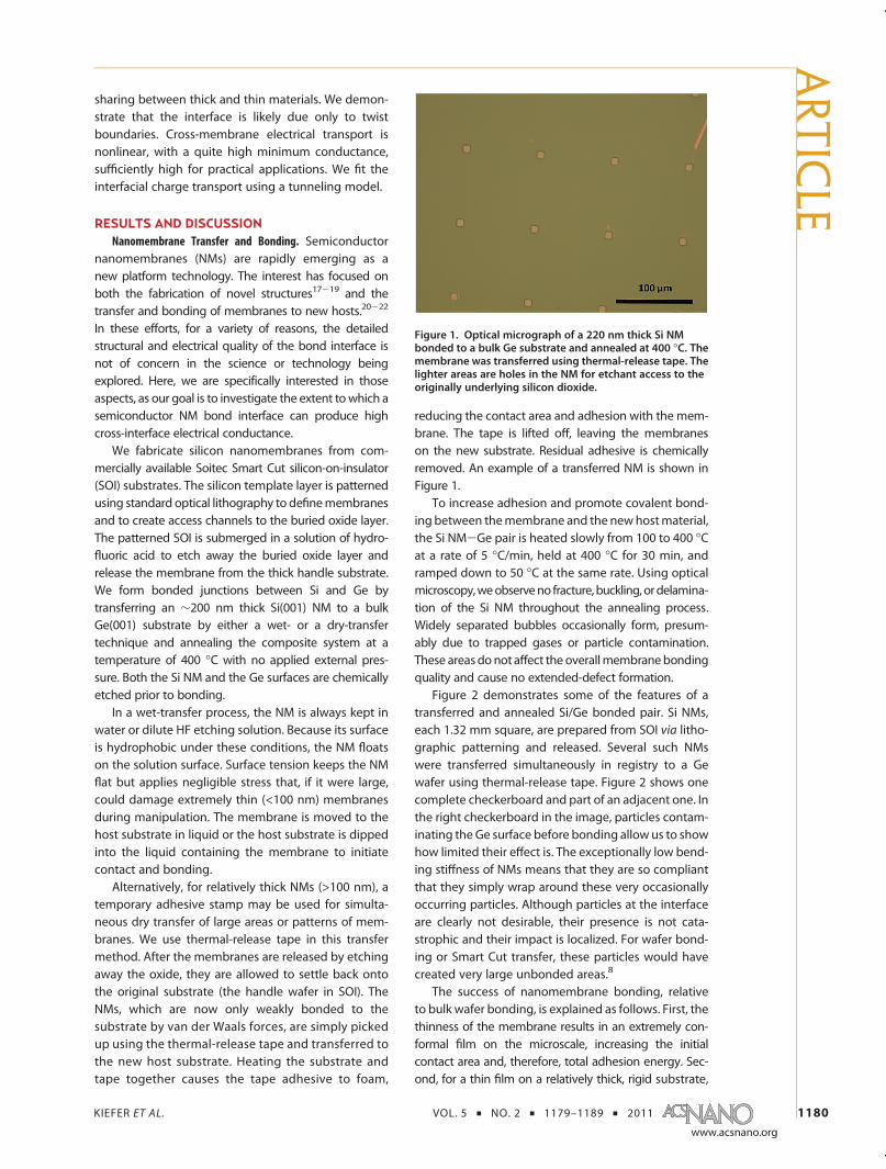
reducing the contact area and adhesion with the mem-brane. The tape is lifted off, leaving the membraneson the new substrate. Residual adhesive is chemicallyremoved. An example of a transferred NM is shown inFigure 1.
To increase adhesion and promote covalent bond-ing between themembrane and the newhostmaterial,the Si NM-Ge pair is heated slowly from 100 to 400 �Cat a rate of 5 �C/min, held at 400 �C for 30 min, andramped down to 50 �C at the same rate. Using opticalmicroscopy,weobserveno fracture,buckling, ordelamina-tion of the Si NM throughout the annealing process.Widely separated bubbles occasionally form, presum-ably due to trapped gases or particle contamination.These areasdo not affect the overallmembranebondingquality and cause no extended-defect formation.
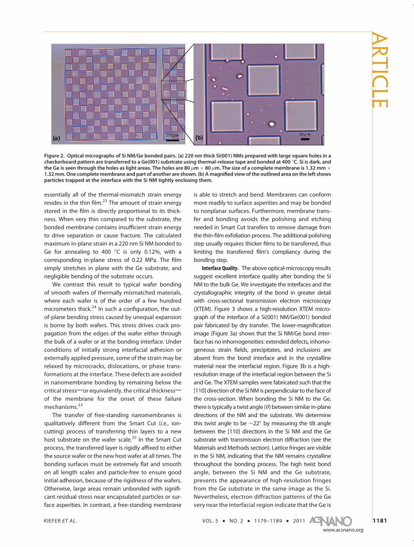
Figure 2 demonstrates some of the features of atransferred and annealed Si/Ge bonded pair. Si NMs,each 1.32 mm square, are prepared from SOI via litho-graphic patterning and released. Several such NMswere transferred simultaneously in registry to a Gewafer using thermal-release tape. Figure 2 shows onecomplete checkerboard and part of an adjacent one. Inthe right checkerboard in the image, particles contam-inating the Ge surface before bonding allow us to showhow limited their effect is. The exceptionally low bend-ing stiffness of NMs means that they are so compliantthat they simply wrap around these very occasionallyoccurring particles. Although particles at the interfaceare clearly not desirable, their presence is not cata-strophic and their impact is localized. For wafer bond-ing or Smart Cut transfer, these particles would havecreated very large unbonded areas.8
The success of nanomembrane bonding, relativeto bulk wafer bonding, is explained as follows. First, thethinness of the membrane results in an extremely con-formal film on the microscale, increasing the initialcontact area and, therefore, total adhesion energy. Sec-ond, for a thin film on a relatively thick, rigid substrate,
Figure 1. Optical micrograph of a 220 nm thick Si NMbonded to a bulk Ge substrate and annealed at 400 �C. Themembrane was transferred using thermal-release tape. Thelighter areas are holes in the NM for etchant access to theoriginally underlying silicon dioxide.
ARTIC
LE
KIEFER ET AL. VOL. 5 ’ NO. 2 ’ 1179–1189 ’ 2011 1181
www.acsnano.org
essentially all of the thermal-mismatch strain energyresides in the thin film.23 The amount of strain energystored in the film is directly proportional to its thick-ness. When very thin compared to the substrate, thebonded membrane contains insufficient strain energyto drive separation or cause fracture. The calculatedmaximum in-plane strain in a 220 nm Si NM bonded toGe for annealing to 400 �C is only 0.12%, with acorresponding in-plane stress of 0.22 MPa. The filmsimply stretches in plane with the Ge substrate, andnegligible bending of the substrate occurs.
We contrast this result to typical wafer bondingof smooth wafers of thermally mismatched materials,where each wafer is of the order of a few hundredmicrometers thick.24 In such a configuration, the out-of-plane bending stress caused by unequal expansionis borne by both wafers. This stress drives crack pro-pagation from the edges of the wafer either throughthe bulk of a wafer or at the bonding interface. Underconditions of initially strong interfacial adhesion orexternally applied pressure, some of the strainmay berelaxed by microcracks, dislocations, or phase trans-formations at the interface. These defects are avoidedin nanomembrane bonding by remaining below thecritical stress;or equivalently, the critical thickness;of the membrane for the onset of these failuremechanisms.23
The transfer of free-standing nanomembranes isqualitatively different from the Smart Cut (i.e., ion-cutting) process of transferring thin layers to a newhost substrate on the wafer scale.25 In the Smart Cutprocess, the transferred layer is rigidly affixed to eitherthe source wafer or the new host wafer at all times. Thebonding surfaces must be extremely flat and smoothon all length scales and particle-free to ensure goodinitial adhesion, because of the rigidness of the wafers.Otherwise, large areas remain unbonded with signifi-cant residual stress near encapsulated particles or sur-face asperities. In contrast, a free-standing membrane
is able to stretch and bend. Membranes can conformmore readily to surface asperities and may be bondedto nonplanar surfaces. Furthermore, membrane trans-fer and bonding avoids the polishing and etchingneeded in Smart Cut transfers to remove damage fromthe thin-film exfoliation process. The additional polishingstep usually requires thicker films to be transferred, thuslimiting the transferred film's compliancy during thebonding step.
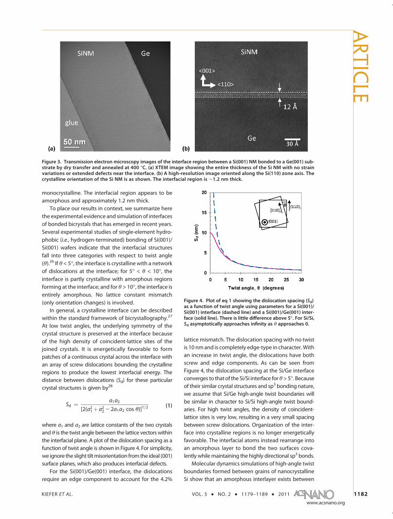
Interface Quality. The above optical-microscopy resultssuggest excellent interface quality after bonding the SiNM to the bulk Ge. We investigate the interfaces and thecrystallographic integrity of the bond in greater detailwith cross-sectional transmission electron microscopy(XTEM). Figure 3 shows a high-resolution XTEM micro-graph of the interface of a Si(001) NM/Ge(001) bondedpair fabricated by dry transfer. The lower-magnificationimage (Figure 3a) shows that the Si NM/Ge bond inter-face has no inhomogeneities: extended defects, inhomo-geneous strain fields, precipitates, and inclusions areabsent from the bond interface and in the crystallinematerial near the interfacial region. Figure 3b is a high-resolution image of the interfacial region between the Siand Ge. The XTEM samples were fabricated such that the[110] direction of the Si NM is perpendicular to the face ofthe cross-section. When bonding the Si NM to the Ge,there is typically a twist angle (θ) between similar in-planedirections of the NM and the substrate. We determinethis twist angle to be ∼22� by measuring the tilt anglebetween the [110] directions in the Si NM and the Gesubstrate with transmission electron diffraction (see theMaterials andMethods section). Lattice fringes are visiblein the Si NM, indicating that the NM remains crystallinethroughout the bonding process. The high twist bondangle, between the Si NM and the Ge substrate,prevents the appearance of high-resolution fringesfrom the Ge substrate in the same image as the Si.Nevertheless, electron diffraction patterns of the Gevery near the interfacial region indicate that the Ge is
Figure 2. Optical micrographs of Si NM/Ge bonded pairs. (a) 220 nm thick Si(001) NMs prepared with large square holes in acheckerboard pattern are transferred to a Ge(001) substrate using thermal-release tape and bonded at 400 �C. Si is dark, andthe Ge is seen through the holes as light areas. The holes are 80 μm� 80 μm. The size of a complete membrane is 1.32 mm�1.32mm.One completemembrane and part of another are shown. (b) Amagnified viewof the outlined area on the left showsparticles trapped at the interface with the Si NM tightly enclosing them.
ARTIC
LE
KIEFER ET AL. VOL. 5 ’ NO. 2 ’ 1179–1189 ’ 2011 1182
www.acsnano.org
monocrystalline. The interfacial region appears to beamorphous and approximately 1.2 nm thick.
To place our results in context, we summarize herethe experimental evidence and simulation of interfacesof bonded bicrystals that has emerged in recent years.Several experimental studies of single-element hydro-phobic (i.e., hydrogen-terminated) bonding of Si(001)/Si(001) wafers indicate that the interfacial structuresfall into three categories with respect to twist angle(θ).26 If θ < 5�, the interface is crystalline with a networkof dislocations at the interface; for 5� < θ < 10�, theinterface is partly crystalline with amorphous regionsforming at the interface; and for θ> 10�, the interface isentirely amorphous. No lattice constant mismatch(only orientation changes) is involved.
In general, a crystalline interface can be describedwithin the standard framework of bicrystallography.27
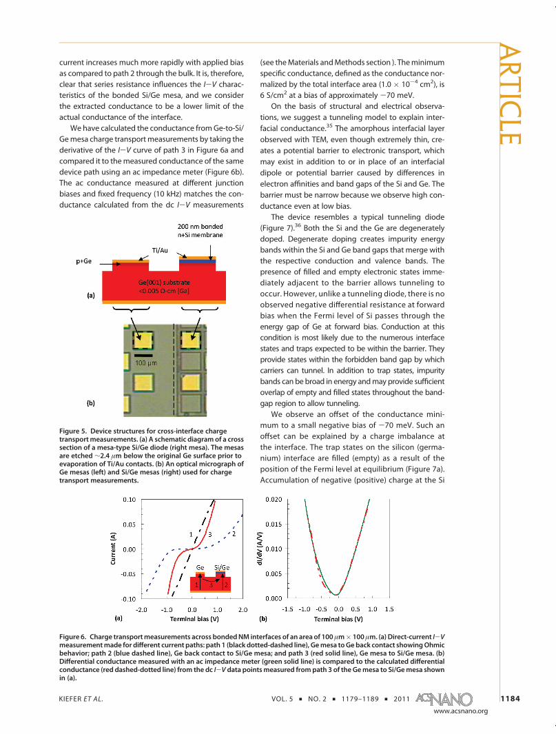
At low twist angles, the underlying symmetry of thecrystal structure is preserved at the interface becauseof the high density of coincident-lattice sites of thejoined crystals. It is energetically favorable to formpatches of a continuous crystal across the interface withan array of screw dislocations bounding the crystallineregions to produce the lowest interfacial energy. Thedistance between dislocations (Sd) for these particularcrystal structures is given by28
Sd ¼ a1a2
[2(a21 þ a22 - 2a1a2 cos θ)]1=2(1)
where a1 and a2 are lattice constants of the two crystalsand θ is the twist angle between the lattice vectors withinthe interfacial plane. A plot of the dislocation spacing as afunction of twist angle is shown in Figure 4. For simplicity,we ignore the slight tiltmisorientation fromthe ideal (001)surface planes, which also produces interfacial defects.
For the Si(001)/Ge(001) interface, the dislocationsrequire an edge component to account for the 4.2%
lattice mismatch. The dislocation spacing with no twistis 10 nmand is completely edge-type in character.Withan increase in twist angle, the dislocations have bothscrew and edge components. As can be seen fromFigure 4, the dislocation spacing at the Si/Ge interfaceconverges to that of the Si/Si interface forθ>5�. Becauseof their similar crystal structures and sp3 bonding nature,we assume that Si/Ge high-angle twist boundaries willbe similar in character to Si/Si high-angle twist bound-aries. For high twist angles, the density of coincident-lattice sites is very low, resulting in a very small spacingbetween screw dislocations. Organization of the inter-face into crystalline regions is no longer energeticallyfavorable. The interfacial atoms instead rearrange intoan amorphous layer to bond the two surfaces cova-lently whilemaintaining the highly directional sp3 bonds.
Molecular dynamics simulations of high-angle twistboundaries formed between grains of nanocrystallineSi show that an amorphous interlayer exists between
Figure 3. Transmission electron microscopy images of the interface region between a Si(001) NM bonded to a Ge(001) sub-strate by dry transfer and annealed at 400 �C. (a) XTEM image showing the entire thickness of the Si NM with no strainvariations or extended defects near the interface. (b) A high-resolution image oriented along the Si(110) zone axis. Thecrystalline orientation of the Si NM is as shown. The interfacial region is ∼1.2 nm thick.
Figure 4. Plot of eq 1 showing the dislocation spacing (Sd)as a function of twist angle using parameters for a Si(001)/Si(001) interface (dashed line) and a Si(001)/Ge(001) inter-face (solid line). There is little difference above 5�. For Si/Si,Sd asymptotically approaches infinity as θ approaches 0.
ARTIC
LE

KIEFER ET AL. VOL. 5 ’ NO. 2 ’ 1179–1189 ’ 2011 1183
www.acsnano.org
grains.29 The calculated radial density function forthese interlayers is practically identical to that of bulkamorphous Si. The principal conclusion of these simu-lations is that the amorphous interlayer is energeticallylower than alternative interfaces, making it the ther-modynamically preferred state for twist angles greaterthan 10�. Otsuki measured the interfacial energy be-tween Si(001) twist boundaries from 0� to 45� andfound that the interfacial energy for twist angles >10�was nearly constant, in agreement with the simula-tions.30 The simulations also predict that the interlayertends to be between 4 and 8 ML (monolayers) thick,independent of twist angle. The vast majority of Siatoms within the amorphous layer is 4-fold coordi-nated with less than 10% of them either 3- or 5-foldcoordinated, indicating that the density of danglingbonds near the interface is less extensive than onemayinitially expect. The low stiffness of NMs makes it likelythat the interface region is as least as small, andpossibly smaller, than for bulk crystals.
Thus far, we have only considered geometricalrelationships for predicting the structure of the inter-face. Si and Ge constitute a fully miscible binary alloysystem, and interdiffusion could, in principle, drivemorphological changes of the interface. Interdiffusionis, however, unlikely to be significant at the tempera-tures and times used in our experiments. As an exam-ple, thediffusivity of Si in Ge is on theorder of 1019 cm2/sat 550 �C.31 Assuming the same diffusivity at a muchlower 400 �C, the diffusion length is on the order of 1 Åin 30 min. Although the more open structure of theinterface may enhance diffusion, diffusion beyond theinterfacial layer is negligible.
Additionally, interfacial contamination could, inprinciple, play a role. Because our surfaces are hydro-phobic, we can rule out most contamination possibi-lities, even though the initial contact between ourbonded surfaces occurs in an ambient atmosphere.Hydrophobic bonding generally produces thinner in-terfacial layers or crystalline interfaces with minimalextrinsic defects.32 However, hydrophobic surfaces inbulk wafer bonding generally produce interfaces withlow adhesive energy and require higher annealing tem-peratures to create strong interfacial bonding. For full-wafer bonding, thermal-expansion mismatch limitsannealing temperatures to values below those neces-sary to form sufficiently strong interfaces. In contrast,NMs are ultracompliant and are able to maximize thecontact area with the host substrate and to stretchwithout creation of defects at higher thermal-mis-match strain. Consequently, the benefits of hydropho-bic bonding are available to NM bonding. Any low-temperature bonding scheme employing hydrophilicor plasma treated surfaces will likely produce widerinterfaces, due to incorporation of other elements.33,34
The measured interfacial conductivity of bonded hy-drophobic Si/Si wafers is clearly superior to hydrophilic
bonding for this reason.32 If electrical conductionacross the interface is desired, hydrophilic bonding,even though it is much easier in bulk materials, iscounterproductive. As we demonstrate here with NMs,hydrophobic bonding produces excellent interfaces.
We conclude that the bonded Si/Ge interface struc-ture is a thin amorphous layer created by twist bound-aries. This interfacial region is thermodynamically stableand only a few lattice constants wide, owing to thestrong sp3 bonding, which drives atomic reorganiza-tion at the interface. Interdiffusion will be insignificantfor the range of temperatures and times under con-sideration. Because our Ge and Si NMs are hydrogen-terminated, contamination is minimal and does notlikely contribute to the interface width.Electrical Characterization. Membrane bonding in the
manner described above creates a narrow interfacialregion with a high density of atomic defects. Simplis-tically, any interface creates a barrier to charge trans-port. In principle, the interface can always be mademore resistive by deliberately adding an interfacialdielectric layer. We attempt to minimize the dielectriclayer to make the cross-barrier conductivity high, andour narrower interface, relative to conventional waferbonding of Si and Ge, presents that opportunity.33,34
To investigate cross-interface conduction, we use a200 nm nþ-Si NM (4� 1020/cm3) bonded to a pþ-Gewafer (>1 � 1020/cm3) and annealed at 400 �C for 30min (see the Materials and Methods section). Highdoping reduces depletion regions, thus better definingthe interface electrically, and ensures a high density ofmobile carriers for enhanced charge transport.
After transferring the Si NM, we create 100 μm �100 μm mesas of Ge and Si/Ge and deposit metalcontacts, as depicted in Figure 5. Current-voltage(I-V) characteristics are then measured from mesa tomesa. Positive bias is defined with respect to the Sicontact as ground. Typical results of dc I-V measure-ments are shown in Figure 6a. The maximum relativeerrors were 0.3% for current and 0.01% for voltage atzero applied bias with no dependence on the polarityof the swept voltage. There was no appreciable differ-ence in curves from pads measured at adjacent sites.
We confirmed that Si contacts were Ohmic onseparate control devices formed using the same SOIsubstrate from which the Si NMs were fabricated. dccurrent-voltage measurements of bonded Si/Ge in-terfaces are shown in Figure 6a for three differentcurrent paths defined in the inset. Path 1 is from abottom contact on the Ge bulk substrate to a Ge mesacontact on the top; the curve confirms Ohmic conduc-tion through the bulk Ge wafer and Ge contacts. Path 2is from the bottom Ge contact to a Si/Ge mesa contacton the top; at high biases, the current parallels path 1,indicating that conduction has become limited by theseries resistance of the bulk substrate. Path 3 is fromthe top Gemesa contact to the Si/Gemesa contact; the
ARTIC
LE
KIEFER ET AL. VOL. 5 ’ NO. 2 ’ 1179–1189 ’ 2011 1184
www.acsnano.org
current increases much more rapidly with applied biasas compared to path 2 through the bulk. It is, therefore,clear that series resistance influences the I-V charac-teristics of the bonded Si/Ge mesa, and we considerthe extracted conductance to be a lower limit of theactual conductance of the interface.
We have calculated the conductance fromGe-to-Si/Gemesa charge transportmeasurements by taking thederivative of the I-V curve of path 3 in Figure 6a andcompared it to themeasured conductance of the samedevice path using an ac impedance meter (Figure 6b).The ac conductance measured at different junctionbiases and fixed frequency (10 kHz) matches the con-ductance calculated from the dc I-V measurements
(see theMaterials andMethods section ). Theminimumspecific conductance, defined as the conductance nor-malized by the total interface area (1.0 � 10-4 cm2), is6 S/cm2 at a bias of approximately -70 meV.
On the basis of structural and electrical observa-tions, we suggest a tunneling model to explain inter-facial conductance.35 The amorphous interfacial layerobserved with TEM, even though extremely thin, cre-ates a potential barrier to electronic transport, whichmay exist in addition to or in place of an interfacialdipole or potential barrier caused by differences inelectron affinities and band gaps of the Si and Ge. Thebarrier must be narrow because we observe high con-ductance even at low bias.
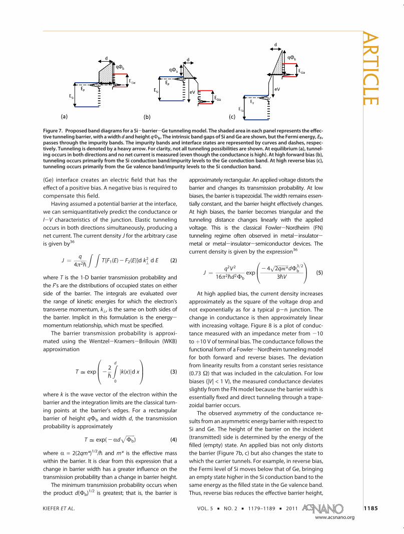
The device resembles a typical tunneling diode(Figure 7).36 Both the Si and the Ge are degeneratelydoped. Degenerate doping creates impurity energybands within the Si and Ge band gaps that merge withthe respective conduction and valence bands. Thepresence of filled and empty electronic states imme-diately adjacent to the barrier allows tunneling tooccur. However, unlike a tunneling diode, there is noobserved negative differential resistance at forwardbias when the Fermi level of Si passes through theenergy gap of Ge at forward bias. Conduction at thiscondition is most likely due to the numerous interfacestates and traps expected to be within the barrier. Theyprovide states within the forbidden band gap by whichcarriers can tunnel. In addition to trap states, impuritybands can be broad in energy andmay provide sufficientoverlap of empty and filled states throughout the band-gap region to allow tunneling.
We observe an offset of the conductance mini-mum to a small negative bias of -70 meV. Such anoffset can be explained by a charge imbalance atthe interface. The trap states on the silicon (germa-nium) interface are filled (empty) as a result of theposition of the Fermi level at equilibrium (Figure 7a).Accumulation of negative (positive) charge at the Si
Figure 6. Charge transportmeasurements across bondedNM interfaces of an area of 100 μm� 100μm. (a) Direct-current I-Vmeasurementmade for different current paths: path 1 (black dotted-dashed line), Gemesa toGe back contact showingOhmicbehavior; path 2 (blue dashed line), Ge back contact to Si/Ge mesa; and path 3 (red solid line), Ge mesa to Si/Ge mesa. (b)Differential conductance measured with an ac impedance meter (green solid line) is compared to the calculated differentialconductance (red dashed-dotted line) from the dc I-V data pointsmeasured frompath 3 of the Gemesa to Si/Gemesa shownin (a).
Figure 5. Device structures for cross-interface chargetransportmeasurements. (a) A schematic diagramof a crosssection of a mesa-type Si/Ge diode (right mesa). The mesasare etched ∼2.4 μm below the original Ge surface prior toevaporation of Ti/Au contacts. (b) An optical micrograph ofGe mesas (left) and Si/Ge mesas (right) used for chargetransport measurements.
ARTIC
LE
KIEFER ET AL. VOL. 5 ’ NO. 2 ’ 1179–1189 ’ 2011 1185
www.acsnano.org
(Ge) interface creates an electric field that has theeffect of a positive bias. A negative bias is required tocompensate this field.
Having assumed a potential barrier at the interface,we can semiquantitatively predict the conductance orI-V characteristics of the junction. Elastic tunnelingoccurs in both directions simultaneously, producing anet current. The current density J for the arbitrary caseis given by36
J ¼ q
4π2p
Z ZT[F1(E)- F2(E)]d k2^ d E (2)
where T is the 1-D barrier transmission probability andthe F's are the distributions of occupied states on eitherside of the barrier. The integrals are evaluated overthe range of kinetic energies for which the electron'stransverse momentum, k^, is the same on both sides ofthe barrier. Implicit in this formulation is the energy-momentum relationship, which must be specified.
The barrier transmission probability is approxi-mated using the Wentzel-Kramers-Brillouin (WKB)approximation
T = exp -2p
Zd
0
jk(x)jd x
0B@
1CA (3)
where k is the wave vector of the electron within thebarrier and the integration limits are the classical turn-ing points at the barrier's edges. For a rectangularbarrier of height qΦb and width d, the transmissionprobability is approximately
T = exp(-RdffiffiffiffiffiffiffiΦb
p) (4)
where R = 2(2qm*)1/2/p and m* is the effective masswithin the barrier. It is clear from this expression that achange in barrier width has a greater influence on thetransmission probability than a change in barrier height.
The minimum transmission probability occurs whenthe product d(Φb)
1/2 is greatest; that is, the barrier is
approximately rectangular. An applied voltage distorts thebarrier and changes its transmission probability. At lowbiases, the barrier is trapezoidal. The width remains essen-tially constant, and the barrier height effectively changes.At high biases, the barrier becomes triangular and thetunneling distance changes linearly with the appliedvoltage. This is the classical Fowler-Nordheim (FN)tunneling regime often observed in metal-insulator-metal or metal-insulator-semiconductor devices. Thecurrent density is given by the expression36
J ¼ q2V2
16π2pd2Φbexp
- 4ffiffiffiffiffiffiffiffiffiffiffi2qm�p
dΦ3=2b
3pV
0@
1A (5)
At high applied bias, the current density increasesapproximately as the square of the voltage drop andnot exponentially as for a typical p-n junction. Thechange in conductance is then approximately linearwith increasing voltage. Figure 8 is a plot of conduc-tance measured with an impedance meter from -10toþ10 V of terminal bias. The conductance follows thefunctional form of a Fowler-Nordheim tunnelingmodelfor both forward and reverse biases. The deviationfrom linearity results from a constant series resistance(0.73 Ω) that was included in the calculation. For lowbiases (|V| < 1 V), the measured conductance deviatesslightly from the FNmodel because the barrier width isessentially fixed and direct tunneling through a trape-zoidal barrier occurs.
The observed asymmetry of the conductance re-sults from an asymmetric energy barrier with respect toSi and Ge. The height of the barrier on the incident(transmitted) side is determined by the energy of thefilled (empty) state. An applied bias not only distortsthe barrier (Figure 7b, c) but also changes the state towhich the carrier tunnels. For example, in reverse bias,the Fermi level of Si moves below that of Ge, bringingan empty state higher in the Si conduction band to thesame energy as the filled state in the Ge valence band.Thus, reverse bias reduces the effective barrier height,
Figure 7. Proposed band diagrams for a Si-barrier-Ge tunnelingmodel. The shaded area in each panel represents the effec-tive tunneling barrier, with awidth d and height qΦb. The intrinsic band gaps of Si andGe are shown, but the Fermi energy, EF,passes through the impurity bands. The impurity bands and interface states are represented by curves and dashes, respec-tively. Tunneling is denoted by a heavy arrow. For clarity, not all tunneling possibilities are shown. At equilibrium (a), tunnel-ing occurs in both directions and no net current is measured (even though the conductance is high). At high forward bias (b),tunneling occurs primarily from the Si conduction band/impurity levels to the Ge conduction band. At high reverse bias (c),tunneling occurs primarily from the Ge valence band/impurity levels to the Si conduction band.
ARTIC
LE

KIEFER ET AL. VOL. 5 ’ NO. 2 ’ 1179–1189 ’ 2011 1186
www.acsnano.org
increasing the tunneling probability. Other factorsthat may affect asymmetry in conductance includethe effective masses of carriers, the dielectric con-stants, and the density of states of the Si, Ge, andinterfacial layer.
A tunneling model can explain the trends ininterfacial conductance by correlating current withbarrier transmission probability, and a numerical fitcan yield physically reasonable parameters. However,the fit is not unique based solely on these databecause of the mathematical interdependencies ofthe parameters within the model. A precise, quanti-tative extraction of interfacial properties frommodeling requires extreme caution for several rea-sons: (1) Our simplified model does not explicitlyaddress the different band structures of Si and Ge.As both are indirect-gap semiconductors, inelasticprocesses are required to conserve momentum dur-ing tunneling. This added constraint should dramati-cally reduce the tunneling current. (2) Knowledge ofthe distribution of the interface states, both spatiallyand energetically, is presently inadequate to estimatetheir role quantitatively in conduction. We expect∼1013/cm2 unsatisfied or strained Si bonds at theinterface because Si has a higher planar density ofatoms than Ge. This high number of states in combina-tion with the high degree of atomic disorder within thebarrier makes it unlikely that a single, uniform barrierpotential will apply across the entire interface. A smallfractional change in barrier width locally can causedramatic changes in current density, making homoge-neous current flow across the interface unlikely. (3) Theeffectivemass of carriers within the barrier is unknown. Ithas been shown that energy-momentum dispersionrelations of a disordered barrier cannot be accuratelydetermined solely by analysis of conductance curves.37
Because of the general overwhelming difficulty informing bonded Si/Ge structures, measurements ofelectrical transport across bonded Si/Ge interfaces tocompare to ours are scarce. The difference in interfacestructural and chemical quality makes a quantitativecomparison futile in any case. However, as an example,Zahler et al. employed a pþ-Ge layer bonded to apþ-Si substrate and report an interfacial resistance of400 Ω cm2.11 By comparison, the resistance of ourbonded nþ-Si NM/pþ-Ge junction is significantly less,< 1Ω cm2, of considerable value for high-current-densityapplications, such as photovoltaics, where high inter-facial conductance is crucially important to reduceresistive losses.10 In general, we can state that ourmembrane bonded junction conducts very well, wellenough, even without optimization, for many applica-tions that require electronic transport across a bondedheterojunction. Thus, nanomembranebondingcan serveas the basis of optoelectronic devices, such as a Si/Getandem solar cell, a Si/Ge/Si PIN photodetector, or Si/Ge light emitters.
Wehave not so far attempted to optimize interfacialconductance. We expect that even higher conductancecanbeachievedbyappropriate surfacepreparationpriorto bonding and by optimizing thermal treatments.Furthermore, postbonding interface modification, suchas annealing in forming gas, may lead to a modificationof the barrier and thus different I-V characteristics withpresumably higher currents.
CONCLUSIONS
We show successful bonding of a 200 nm thickcrystalline Si sheet to a bulk Ge substrate using hydro-phobic bonding, characterize the bonding interface,and fabricate diode device structures on this bondedpair to explore cross-interface electrical transport. Noindication of separation, fracture, or strain inhomo-geneity is observed, demonstrating that NMbonding isan effective and viable method to join highly latticemismatched materials. XTEM measurements show avery well defined, extremely narrow interface region,controlled by structure rather than interface chemistry,because NM bonding is successful even if hydrophobicsurfaces are bonded. Hydrophobic bonding of nano-membranes thus offers a new direction for integrationof materials for novel hybrid electronic devices thatcircumvents the serious problems associated with bulkwafer bonding. Our nanomembrane bonded devicesare nonlinear and give a minimum specific conduc-tance of 6 S/cm2 without any effort at optimization.Our structural and electronic study of bonded Si/Ge
nanomembranes, a material combination that hasresisted conventional approaches, makes novel Si/Gedevices that require cross-interface conduction a rea-listic possibility. More generally, one can expect toextend nanomembrane bonding to other material
Figure 8. ac conductance as a function of terminal bias. Thedata (blue dots) are fit applying only a Fowler-Nordheimtunneling model (red solid line) assuming a barrier widthof 1.2 nm and a series resistance of 0.73Ω. In forward bias,Φb = 1.27 eV andm*=0.0170me; in reversebias,Φb = 1.94 eVand m* = 0.8354 me.
ARTIC
LE
KIEFER ET AL. VOL. 5 ’ NO. 2 ’ 1179–1189 ’ 2011 1187
www.acsnano.org
combinations, with similar beneficial outcomes. Withthe current rapid progress in the manipulation, trans-fer, and stacking of nanomembranes,38 the high-quality
interfaces obtained in nanomembrane bonding makeit likely that a new generation of flexible, high-performancesemiconductor devices will be enabled.
MATERIALS AND METHODSMembrane Fabrication. Silicon nanomembranes are fabricated
from commercially available Soitec Smart Cut silicon-on-insu-lator (SOI) substrates with a 220 nm Si(001) template layer on3 μm of buried silicon dioxide. Thinner buried oxides may beused. Prior to fabrication, the membranes are ion-implantedand annealed (see below). Annealing reduces the membranethickness ∼20 nm by oxidation. Standard optical lithography isused to definemembranes of various lateral sizes and shapes, aswell as etchant access holes. Reactive-ion etching using SF6 orCF4 þ O2 removes exposed silicon. The photoresist is removedby soaking in acetone for 10 min using ultrasonication or bypressurized spray. The patterned SOI pieces are cleaned usingH2SO4/H2O2 (1:1) solution in a quartz beaker for 5 min andrinsed in flowing deionized water for 5 min. Particles andresidual organic contamination are removed by soaking in amixture of NH4OH/H2O2/H2O (1:1:5) for 10 min at 80( 5 �C andagain rinsed in flowing deionizedwater for 5min. The pieces arethen placed in concentrated HF (49%) in a Teflon beaker to situndisturbed to release the Si template layer by differentialetching of the buried oxide layer. Etching time varies dependingon the thickness of the buried oxide and the required etchdistance. Typical etching times are 45 ( 10 min for concen-trated HF.
Wet-Transfer Technique. Soon after the complete dissolution ofthe buried oxide layer, Si membranesmay float off the substrateand onto the surface of the liquid solution due to their hydro-phobic (H-terminated) surfaces. Frequently, they collapse backonto the original handle substrate during the underetchingprocess and remain weakly bonded. Slight agitation mayrelease them into the liquid. The membranes are then pickedout of the water either with Teflon tweezers by electrostaticattraction or by use of a small loop of plastic-coated wire(28 gauge). A water film across the loop provides a surface onwhich the membrane lies. The membrane is then brought intocontact with the new host substrate. Alternatively, the newsubstrate may be dipped into the beaker with the membraneand pulled out, thus drawing the membrane to the surface bycapillary forces. The substrate with membrane is then set on ahot plate at ∼110 �C for at least 10 min to allow evaporation ofwater and to increase initial bonding strength. Usually, anywrinkles in the membrane will smooth out as the shiftinginterface dries. The final placement and orientation of themembrane is difficult to control using this technique.
Dry-Transfer Technique. Nitto Denko Revalpha Thermal ReleaseTape (No. 3198LS) may be used to transfer nanomembranes ofreasonable thickness (∼200 nm) and lateral dimensions on theorder of millimeters. The membranes are underetched in HFsolution and allowed to collapse onto the original handle sub-strate. The handle with membranes is then removed from theHF solution and slowly dipped into deionized water to removeresidual HF. The substrate with membranes is removed fromthe water. The thermal-release tape is placed directly on top ofthe membranes without pressing. An adhesion front starting atthe point of first contact spontaneously spreads across the tape/substrate interface. When themembranes are fully adhered, thetape is carefully peeled with minimum bending, to preventmembrane fracture. Frequently, membranes near the initialpeeling edge will crack. The tape with membranes is immedi-ately placed on the new substrate without pressing. A slightbending of the tape will usually ensure only one point or line ofcontact. The adhesion front is allowed to progress sponta-neously and often occurs in <10 min for a 1 cm2 area. Thesubstrate with tape is then placed on a preheated hot plate just
above the tape's release temperature (∼100 �C). After the tapedebonds, the tape is lifted off the substrate. Removal of residualadhesive using photoresist stripper (e.g., AZ 300T from AZElectronic Materials) for Ge substrates is possible, and is donebefore high-temperature annealing. Very thin membranescannot be transferred using this technique as the membranesconform to the foaming adhesive layer of the tape rather thanadhering to the new substrate.
Ion Implantation. Before membrane fabrication, the Si tem-plate layer of the SOI is ion-implanted (Core Systems, California)with P (dose is 1� 1016/cm2 at an energy of 12 keV with a 7� tilt)and annealed in N2 at 950 �C for 45 min to achieve a uniformdopant concentration of 4� 1020/cm3 throughout the templatelayer thickness, as measured by secondary-ion mass spectros-copy (Evans Analytical Group, NJ). Sheet resistance measure-ments by transfer length and Greek cross methods confirm theexpected carrier concentration.39 The as-received Ge waferswere p-type (Ga) with a resistivity of 0.005Ω 3 cm. We addition-ally doped the top 50 nm degenerately to >1 � 1020/cm3 withGa by ion implantation (dose is 3� 1015/cm2 at 40 keV with a 7�tilt). The dopant concentration was also measured by secondary-ionmass spectroscopy. Prior to implantation, 10 nmof PECVDSiO2
is deposited on theGe surface to ensure shallow implantation. Theimplanted Ge is annealed in a rapid thermal annealing tool at600 �C for 1 min.40
Germanium Preparation. It is essential that the Ge substrateremain particle-free to avoid trapping particles at the interface.Once diced or cleaved, the brittle edges of germanium becomea persistent source of particle contamination, so whole 2 in.wafers are used whenever possible. Just prior to transfer of thenanomembrane, the deposited and native oxides on the Ge areremoved in a mixture of HF/HCl/H2O (1:1:10).41,42
Thermal Annealing. Bonded pairs are heated directly on aprogrammable hot plate or in a convection oven in nitrogenambient. The temperature is ramped from100 to 400 �C at a rateof 5 �C/min, held at 400 �C for 30 min, and ramped down to50 �C at the same rate. No pressure is applied to the sampleduring the annealing step.
Mesa Device Fabrication. Wedefine 100 μm� 100 μmmesas ofGe and Si with optical lithography and reactive-ion etchingusing CF4þO2. We then deposit 90 μm� 90 μmmetal contactspads of 500 Å/5000 Å Ti/Au by evaporation onto the mesas anduse a standard lift-off technique. No contact annealing wasperformed.
All fabrication processes are carried out in a Class 100 cleanroom to avoid particulate contamination.
Electrical Measurements. I-V measurements were performedon a probe station using a Keithley 2400 Source Metering Unit.The current range of the measurement was -100 to þ100 mA,limited by the compliancy of the instrument. To establishprecision, the bias was swept back-and-forth 10 consecutivetimes with alternating polarity. The relative error was deter-mined by dividing the standard deviation by the average of themeasurements at a given point. ac conductance measurementswere made using an Agilent 4284A Precision LCR Meter. The acsignal amplitude was 10mV, and a dc bias across the devicewasswept from-10 toþ10 V. The ac frequencywas varied from100Hz to 1 MHz but held constant during each voltage sweep. Themeasured admittance was decomposed into conductance andsusceptance. The conductance was essentially independent offrequency; however, the measurements are typically made at10 kHz to reduce coupling with parasitic impedance.
The series resistance of a test device is estimated bymeasuring the slope of the dc I-V curve at high bias or bymeasurement using the ac impedance meter. The measured
ARTIC
LE
KIEFER ET AL. VOL. 5 ’ NO. 2 ’ 1179–1189 ’ 2011 1188
www.acsnano.org
complex impedance is decomposed into resistance and reac-tance components. The series resistance depends on the mea-surement instrument, method of connection, and current path,as this is a two-terminal measurement.
Cross-Sectional Transmission Electron Microscopy (XTEM). The XTEMsamples were prepared by mechanical polishing and ionmilling. The samples were initially thinned to 8-10 μm viamechanical polishing and dimplingwith diamond lapping films.The samples were further thinned with Arþ ion milling to makethem electron transparent. The ion milling energies were prog-ressively reduced (from 4 to 1 keV) to minimize the depth of theamorphous layer on the surface of the sample. The sampleswere characterized on a Philips CM200 TEM with a 200 keVoperating voltage.
The twist angle between the Si NM and theGe substrate wasobtained by measuring the tilt angle between the (110) zoneaxis of the Si NM and the (130) zone axis of the Ge substrate. Thetwist angle was then extrapolated from knowledge of the actualangle between the (110) and (130) zone axes. Any miscut fromthe [001] direction of the surface of the Si NM or the Gesubstrate was not accounted for in determining the approx-imate twist angle.
Acknowledgment. We thank G. Sun, Z. Q. Ma, and K. Turnerfor advice and S. Babcock for access to facilities. This researchwas primarily supported by AFOSR (Nanomembrane MURI,Grant No. FA9550-08-1-0337). The TEM and other structuralcharacterizations (D.M.P. and A.M.C.) were supported by theDOE (Grant No. DE-FG02-03ER46028). A.M.K. is supported by aDoD SMART Scholarship, and D.M.P. is supported by an NSFGraduate Research Fellowship.We acknowledge facility supportfrom NSF/MRSEC and from AFRL Hanscom.
REFERENCES AND NOTES1. Demeester, P.; Pollentier, I.; De Dobbelaere, P.; Brys, C.; Van
Daele, P. Epitaxial Lift-Off and Its Applications. Semicond.Sci. Technol. 1993, 8, 1124–1135.
2. Chan, W. K.; Yablonovitch, E. In Integrated Optoelectronics;Dagenais, M., Leheny, R. F., Crow, J., Eds.; Academic Press:New York, 1995; pp 297-313.
3. Jokerst, N. M.; Brooke, M. A.; Vendier, O.; Wilkinson, S.; Fike,S.; Lee, M.; Twyford, E.; Cross, J.; Buchanan, B.; Wills, S. Thin-Film Multimaterial Optoelectronic Integrated Circuits. IEEETrans. Compon., Packag., Manuf. Technol., Part B 1996, 19,97–106.
4. Spearing, S. M. Materials Issues in MicroelectromechanicalSystems (MEMS). Acta Mater. 2000, 48, 179–196.
5. Matthews, J. W.; Blakeslee, A. E. Defects in Epitaxial Multi-layers. I. Misfit Dislocations. J. Cryst. Growth 1974, 27118–125.
6. Milnes, A. G.; Feucht, D. L. Heterojunctions and Metal-Semi-conductor Junctions; Academic Press: New York, 1972.
7. Kressel, H. Materials for Heterojunction Devices. Annu. Rev.Mater. Sci. 1980, 10, 287–309.
8. Pl€ossl, A.; Krauter, G. Wafer Direct Bonding: TailoringAdhesion between Brittle Materials. Mater. Sci. Eng., R1999, R25, 1–88.
9. Slack, G. A.; Bartram, S. F. Thermal Expansion of SomeDiamondlike Crystals. J. Appl. Phys. 1975, 46, 89–98.
10. Sun, G.; Chang, F.; Soref, R. A. High Efficiency Thin-FilmCrystalline Si/Ge Tandem Solar Cell.Opt. Express 2010, 18,3746–3753.
11. Zahler, J. M.; Ahn, C.; Zaghi, S.; Atwater, H. A.; Chu, C.; Iles, P.Ge Layer Transfer to Si for Photovoltaic Applications.Proceedings of Symposium P on Thin Film Materials forPhotovoltaics; Materials Research Society: Warrendale, PA;2001; Vol 681E, pp 63-68.
12. Kanbe, H.; Komatsu, M.; Miyaji, M. Ge/Si HeterojunctionPhotodiodes Fabricated by Wafer Bonding. Jpn. J. Appl.Phys. 2006, 45, L644–L646.
13. Colace, L.; Assanto, G. Germanium on Silicon for Near-Infrared Light Sensing. IEEE Photonics J. 2009, 1, 69–79.
14. Sun, X.; Liu, J.; Kimerling, L. C.; Michel, J. Direct GapPhotoluminescence of n-Type Tensile-Strained Ge-on-Si.Appl. Phys. Lett. 2009, 95, 011911.
15. Grenier, K.; Bordas, C.; Pinaud, S.; Salvagnac, L.; Dubuc, D.Germanium Resistors for RF MEMS Based Microsystems.Microsyst. Technol. 2008, 14, 601–606.
16. Scott, S. A.; Lagally, M. G. Elastically Strain-SharingNanomembranes: Flexible and Transferable StrainedSilicon and Silicon-Germanium Alloys. J. Phys. D 2007,40, 75–92.
17. Roberts, M. M.; Klein, L. J.; Savage, D. E.; Slinker, K. A.;Friesen, M.; Celler, G.; Eriksson, M. A.; Lagally, M. G. Elas-tically Relaxed Free-Standing Strained-Silicon Nanomem-branes. Nat. Mater. 2006, 5, 388–393.
18. Huang, M.; Boons, C.; Roberts, M.; Savage, D. E.; Lagally,M. G.; Shaji, N.; Qin, H.; Blick, R.; Nairn, J. A.; Liu, F.Nanomechanical Architecture of Strained Bilayer ThinFilms: FromDesign Principles to Experimental Fabrication.Adv. Mater. 2005, 17, 2860–2864.
19. Schmidt, O. G.; Deneke, C.; Manz, Y. M.; Muller, C. Semi-conductor Tubes, Rods and Rings of Nanometer andMicrometer Dimension. Physica E 2002, 13, 969–973.
20. Kim, D.; Xiao, J.; Song, J.; Huang, Y.; Rogers, J. A. Stretch-able, Curvilinear Electronics Based on Inorganic Materials.Adv. Mater. 2010, 22, 2108–2124.
21. Peng, W.; Roberts, M. M.; Nordberg, E. P.; Flack, F. S.;Colavita, P. E.; Hamers, R. J.; Savage, D. E.; Lagally, M. G.;Eriksson, M. A. Single-Crystal Silicon/Silicon Dioxide Multi-Layer Heterostructures Based on Nanomembrane Trans-fer. Appl. Phys. Lett. 2007, 90, 183107.
22. Yuan, H.-C.; Wang, G.; Ma, Z.; Roberts, M. M.; Savage, D. E.;Lagally, M. G. Flexible Thin-Film Transistors on Biaxial- andUniaxial-Strained Si and SiGe Membranes. Semicond. Sci.Technol. 2007, 22, 72–75.
23. Freund, L. B.; Suresh, S. Thin Film Materials: Stress, DefectFormation and Surface Evolution; Cambridge University Press:Cambridge, U.K., 2006; pp 220-311.
24. Kopperschmidt, P.; K€astner., G.; Hesse, D.; Zakharov, N.;G€osele, U. High Bond Energy and ThermomechanicalStress in Silicon on Sapphire Wafer Bonding. Appl. Phys.Lett. 1997, 70, 2972–2974.
25. Moutanabbir, O.; G€osele, U. Heterogeneous Integration ofCompound Semiconductors. Annu. Rev. Mater. Res. 2010,40, 469–500.
26. Rouviere, J. L.; Rousseau, K.; Fournel, F.; Moriceau, H. HugeDifferences Between Low- and High-Angle Twist GrainBoundaries: The Case of Ultrathin (001) Si Films Bonded to(001) Si Wafers. Appl. Phys. Lett. 2000, 77, 1135–1137.
27. Sutton, A. P.; Balluffi, R. W. Interfaces in Crystalline Materials;Clarendon Press: Oxford, U.K., 1995; pp 70-110.
28. Sagalowicz, L.; Rudra, A.; Syrbu, A.; Behrend, J.; Salomonsson,F.; Streubel, K.; Hammar, M.; Bentell, J. Structure of theWaferFused InP (001)-GaAs (001) Interface. Philos. Mag. Lett. 1997,76, 445–452.
29. Phillpot, S. R.; Wolf, D. Grain Boundaries in Silicon fromZero Temperature through Melting. J. Am. Ceram. Soc.1990, 73, 933–937.
30. Otsuki, A. Energies of (001) Twist Grain Boundaries inSilicon. Acta Mater. 2001, 49, 1737–1745.
31. Silvestri, H. H.; Bracht, H.; Hansen, J. L.; Larsen, A. N.; Haller,E. E. Diffusion of Silicon in Crystalline Germanium. Semi-cond. Sci. Technol. 2006, 21, 758–762.
32. Bengtsson, S.; Engstrom, O. Interface Charge Control ofDirectly Bonded Silicon Structures. J. Appl. Phys. 1989, 66,1231–1239.
33. Ki, Y. B.; Ferain, I.; Fleming, P.; Morris, M.; Goorsky, M.;Colinge, C. Low Temperature Germanium to Silicon DirectWafer Bonding Using Free Radical Exposure. Appl. Phys.Lett. 2010, 96, 102110.
34. Kanbe, H.; Hirose, M.; Ito, T.; Taniwaki, M. CrystallographicProperties of Ge/Si Heterojunctions Fabricated by WetWafer Bonding. J. Electron. Mater. 2010, 39, 1248–1255.
35. Shewchun, J.; Temple, V. A. K. Theoretical TunnelingCurrent Characteristics of the SIS (Semiconductor-Insula-tor-Semiconductor) Diode. J. Appl. Phys. 1972, 43, 5051–5061.
36. Sze, S. M.; Ng, K. K. Physics of Semiconductor Devices, 3rd ed.;John Wiley & Sons: Hoboken, NJ, 2007; pp 417-463.
ARTIC
LE
KIEFER ET AL. VOL. 5 ’ NO. 2 ’ 1179–1189 ’ 2011 1189
www.acsnano.org
37. Leipold, W. C.; Feuchtwang, T. E. Theoretical Considera-tions of Band-Structure Determination from Tunneling inThin-Film Heterojunctions. Phys. Rev. B. 1974, 10, 2195–2204.
38. Kim, T.; Carlson, A.; Ahn, J.; Sang, M.W.; Wang, S.; Huang, Y.;Rogers, J. A. Kinetically Controlled, Adhesiveless TransferPrinting Using Microstructured Stamps. Appl. Phys. Lett.2009, 94, 113502.
39. Schroder, D. K. Semiconductor Material and Device Characteri-zation, 3rd ed.; John Wiley & Sons: Hoboken, NJ, 2006; pp17, 146-149.
40. Satta, A.; Simoen, E.; Janssens, T.; Clarysse, T.; De Jaeger, B.;Benedetti, A.; Hoflijk, I.; Brijs, B.; Meuris, M.; Vandervorst, W.Shallow Junction Ion Implantation in Ge and AssociatedDefect Control. J. Electrochem. Soc. 2006, 153, G229–G233.
41. Sun, S.; Sun, Y.; Liu, Z.; Lee, D.; Peterson, S.; Pianetta, P.Surface Termination and Roughness of Ge(100) Cleanedby HF and HCl Solutions. Appl. Phys. Lett. 2006, 88, 1–3.
42. Kim, J.; McVittie, J.; Saraswat, K.; Nishi, Y. PassivationStudies of Germanium Surfaces. Solid State Phenom.2008, 134, 33–36.
ARTIC
LE