Embed Size (px)
Citation preview

76 Bell Labs Technical Journal ◆ Autumn 1997 Copyright 1997. Lucent Technologies Inc. All rights reserved.
The PastThis section presents a historical review of the
technology revolution, from the invention of the first
integrated circuit (IC) to today’s very large scale inte-
gration (VLSI) technology.
IntroductionThe invention of transistor action (electrical signal
amplification) in semiconducting material was a mon-
umental accomplishment that has revolutionized the
world. As with many inventions, the structure of the
original invention has not only evolved, but has also
led to new structures. The first demonstration of tran-
sistor action, the original point-contact transistor, was
soon followed by the invention of the junction bipolar
transistor. This second structure is viewed as the basis
of modern microelectronics, because it laid the foun-
dation for the concept of building an entire electrical
circuit on a single piece of semiconducting material. It
is interesting to recognize, however, that the junction
bipolar transistor and the technology that was devel-
oped to fabricate it led to another type of transistor,
the metal-oxide semiconductor (MOS) transistor.
Both the theory of MOS transistor operation and the
technology associated with its fabrication were derived
from the classic junction bipolar structure and related
research. Today, however, the MOS transistor is the
structure primarily used in the continuing exponential
growth of modern microelectronics.
Early Work on Bipolar Integrated CircuitsThe dramatic technological revolution that
occurred in electronics between 1948 and 1958 cre-
ated a new world. With the invention of the junction
transistor in 1948, the “killer” technology of the vac-
uum tube emerged. The elimination of filaments, with
their high power consumption and low reliability,
allowed electronics to be applied to almost every
aspect of human life.
The existence of the junction transistor as a single-
element device could not survive for very long. The
new goal was to fabricate several transistors and con-
nect them together on a single piece of semiconduct-
♦ Silicon Microelectronics TechnologyJames T. Clemens
Two inventions—the bipolar transistor and the integrated circuit—have fundamen-tally revolutionized the technology of mankind. Within a period of fifty years, themicroelectronics industry has increased the number of transistors fabricated on a sin-gle piece of semiconductor crystal by a factor of about 100 million, that is, 1.0e10+8,a productivity phenomenon unparalleled in the history of technology and mankind.This paper begins with a historical review of that revolution—from the first inte-grated circuit to modern very large scale integration (VLSI) technology—and thenreviews the development of present-day microelectronics manufacturing technology,based on the concept of the “planar process.” The topics covered include silicon crys-tal technology, crystal dopant techniques, silicon oxidation development, lithogra-phy, materials deposition processes, pattern transfer mechanisms, metal interconnecttechnology, and material passivation technology. The paper concludes with a reviewof the major technical and economic issues that face the microelectronics industry todayand discusses the future technical and economic paths that the industry may take.
Bell Labs Technical Journal ◆ Autumn 1997 77
ing material, thereby creating an electrical circuit, now
called the integrated circuit. It took just ten years for
this to happen. In 1958 J. Kilby, employed at the
research laboratories of Texas Instruments, Inc.,
demonstrated the first working bipolar integrated cir-
cuit. The concept of the integrated circuit created the
“Silicon Age,” filled with exponential growth in sci-
ence, technology, and commerce.
Figure 1 shows a cross section of a junction bipo-
lar transistor. Its electrical characteristics are primarily
determined by the bulk (interior) properties of the
semiconductor crystal. Therefore, extensive materials
research and development was conducted to produce
high-quality semiconductor crystals with extremely
low levels of crystal defects and undesirable impurities.
After the initial demonstrations of the bipolar
transistor and the integrated circuit, early attempts at
reproducible fabrication clearly indicated that the
chemical and mechanical treatment of the transistor
crystal surfaces near the active electrical regions could
vary the quality of the semiconductor devices. A sur-
face passivation technology and its associated theory
was needed. This led to extensive research into the
physics of semiconductor surfaces.
During the 1950s, scientists were investigating the
question of which semiconducting material would be
most useful for fabricating general bipolar transistors.
Two Group IV elements from the Periodic Table—sili-
con (Si) and germanium (Ge)—became the leading
candidates, along with several Group III/Group V
compounds—gallium arsenide (GaAs), indium phos-
phide (InPh), and cadmium sulfide (CdS).
Because of its electrical, mechanical, and thermal
properties, Si emerged as the dominant material. Si had
a unique property; it could be easily oxidized to form a
smooth layer of silicon dioxide (SiO2). This material
acted as both a chemical diffusion barrier during device
fabrication and a surface passivation material for elec-
trical operation. The combined use of SiO2 and Si was
described by J. Hoerni1 in 1960 and became known as
the “planar process.” During the early 1960s, a family
of bipolar transistor products—called “transistor transis-
tor logic” (TTL)—was designed and manufactured.
These bipolar transistor products became the industry
standard for system design.
The Invention of the Si Gate MOSFET TransistorThe concept of the insulated gate field-effect tran-
sistor (IGFET), which predates the research on the
junction bipolar transistor, can be traced back to the
1926 research of J. Lilienfeld2 and the 1935 work of O.
Heil.3 Both attempted to create a device that used a
capacitor structure to modulate the majority carriers in
a semiconducting material.
A series of key events culminated in the demon-
stration of the first Si-based metal-oxide-semiconduc-
tor field-effect transistor (MOSFET). In 1955 I. Ross
proposed the concept of the minority carrier MOSFET,
and in 1960 M. Atalla proposed the Si-based MOSFET.
The extensive research on the Si junction bipolar tran-
sistor also resolved many of the technological proper-
ties of SiO2 and the Si/SiO2 interface. Finally, in 1960,
D. Khang and M. Atalla demonstrated the first Si-
based MOSFET.
Panel 1. Abbreviations, Acronyms, and Terms
A/D—analog-to-digital converterCCD—charge-coupled deviceCdS—cadmium sulfideCMOS—complementary metal-oxide semicon-
ductorCMP—chemical–mechanical polishingCVD—chemical vapor depositionD/A—digital-to-analog converterDRAM—dynamic random access memoryDUV—deep ultravioletEBES—electron beam exposure systemGaAs—gallium arsenideGe—germaniumI300I—International 300-mm InitiativeIC—integrated circuitIGFET—insulated gate field-effect transistorInPh—indium phosphideMOS—metal-oxide semiconductorMOSFET—metal-oxide-semiconductor field-
effect transistorPVD—physical vapor depositionSi—siliconSiCl4—silicon chlorideSiN—silicon nitrideSiO2—silicon dioxideTiN—titanium nitrideTTL—transistor transistor logicVLSI—very large scale integration

78 Bell Labs Technical Journal ◆ Autumn 1997
The basic structure of the silicon MOSFET, as illus-
trated in Figure 2, is two isolated p/n junctions in a
silicon surface, overlaid first with a thin SiO2 insulator
and then with a conducting metal layer. Applying a
voltage to the top conducting metal layer (gate) modu-
lates the electrical properties of the Si surface between
the p/n junctions to electrically connect the n-type
parts of each junction. These source and drain junc-
tions then become the contacts for current flow in the
transistor. Varying the gate voltage modulates the con-
PN+
Collectorburied layer
P+
SiO2
PSubstrate
Emittercontact
Basecontact
Collectorcontact
Isolationdiffusion
P+
Si
N+
N+
Figure 1. The n/p/n junction isolated bipolar transistor.
N N
SiO2 SiO2
Metal gate
P
Source Drain
“Off” state
N N
SiO2 SiO2
Metal gate
P
Source Drain
“On” state
Inversion layer
Figure 2. “Off” and “on” states of the n-channel Si MOSFET.

Bell Labs Technical Journal ◆ Autumn 1997 79
ductance between the junctions, thereby amplifying
the electrical signal on the gate. This type of silicon
transistor was simple to build, and its manufacturabil-
ity depended only on an electrically reproducible
Si/SiO2 interface.
During the next several years, the scientific com-
munity engaged in a major technological race to create
the smallest, most cost-effective MOSFET, given the
available materials, chemistry, and patterning capabili-
ties. In 1967 the Si-gate MOSFET was invented. This
device replaced the conducting metal gate of the earlier
Si MOSFET with a layer of conducting polycrystalline
silicon, a major technological advance for MOSFETs and
their use in ICs. Polycrystalline silicon is a refractory
material that allows high-temperature thermal process-
ing to be conducted after the formation of the gate and
also makes possible self-aligned source and drain diffu-
sions (to the gate) and overcoating of the active transis-
tor with high-temperature insulators. The metal
interconnects and contacts could then be optimally
placed to improve circuit density. With such a structure,
a complex IC could be built with just four basic pattern-
ing steps. The landmark Si-gate MOSFET patent was
finally granted to R. Kerwin et al.4 of Bell Labs.
The first Si-gate MOSFETs were p-channel
devices, as shown in Figure 3, with p-type source and
drain regions in an n-type Si substrate. This structure
was initially preferred because the Si/SiO2 interface
tended to have a net positive charge, which did not
seriously affect the transistor and actually helped sup-
press deleterious surface effects exterior to the active
device region.
Yield and Scaling TheoryIn 1964 B. Murphy wrote a comprehensive paper
examining the economic issues of IC yield and packag-
ing.5 He observed that, if a random defect were to
occur during the process of fabricating an array of ICs
on a single Si wafer, one of the ICs in the array would
fail to function. Therefore, not all sites in an array
would yield working ICs. Because all processes of fab-
rication were subject to random defects, the yield of
good ICs would decrease exponentially with the size of
the IC, thereby linking the concepts of yield and elec-
tronic function cost with defect density in manufac-
ture. To fabricate increasingly larger and more
complex ICs, the defect density would have to be
decreased. What followed was the concept of ultra-
clean manufacturing technology.
Polysilicon gate
Contact to polysilicon
P+ source/drain diffusion
Contact to diffusion
Isolation region
Aluminum metallization
Deposited SiO2
AA
Crosssection
Top view
Contact window
SiO2
Si
Figure 3. The transistor structure of the p-channel Si gate.

80 Bell Labs Technical Journal ◆ Autumn 1997
In 1974 R. Dennard approached the question of
the feature size used to manufacture ICs. To further
reduce the cost per electronic function, it became obvi-
ous that smaller dimensions would produce smaller ICs
and increased yield. His analysis of how MOSFET struc-
tures would evolve, as feature size decreased, led to his
classic paper on device scaling, detailing the device
physics of the MOSFET transistors and the resultant
performance benefits.6 By 1974 the basic technical and
economic foundations for the exponential growth of
the Si MOS IC industry had been established.
Growth of Si MOSFET TechnologyFrom the late 1960s to the present (approxi-
mately thirty years), the Si MOS IC industry has been
growing exponentially both in technical complexity
and economic impact. About 1970, while many cor-
porations were developing specific bipolar and MOS
IC products, a small start-up company—Intel Inc.,
founded by R. Noyce, G. Moore, and A. Grove—
introduced two generic IC products, built from a
p-channel Si gate MOSFET IC technology. The first IC
was a small 4-bit microprocessor, named the “4004,”
and the second was a memory circuit, the “1103.”
The 1103 memory circuit comprised 1,024 completely
independent memory cells. Each cell contained three
transistors, including a p/n junction, which was used
to store charge. The memory states were considered
to be either a “1” or a “0.”
Figure 4 illustrates how four memory cells of a
p-channel IC are constructed using the planar process.
The upper left-hand memory cell in Figure 4 shows
the first two masking layers, which form the active
regions of the MOSFETs and a contact for a polysilicon
gate to a drain in the Si substrate. The polysilicon fea-
tures that form the active gates of the transistors and
interconnects among the transistors are shown in the
upper right-hand corner. The lower right-hand corner
Dataline
Bitline
Writeline
Readline
Thin oxide
Polysilicon contact
Polysilicon lines
Contact window
Aluminum
Aluminum to silicon contact
Figure 4. Schematic and physical layout of the three-transistor cell.

Bell Labs Technical Journal ◆ Autumn 1997 81
shows the contact windows defined in the insulator,
which overlays the polysilicon gates; the lower left-
hand corner shows the metallization contacts and
interconnects that complete the cell structure of the IC.
Because Si p/n junctions have a small current flow
when reverse biased, the information in the cell has to
be refreshed every few milliseconds. Although this
time interval may seem short, it was very long in
terms of the clocking frequency of the circuit, about
5 MHz. The 1103 memory circuit—called a dynamic
random access memory (DRAM)—contained about
5,000 transistors and introduced the concept of large
scale integration. The initial microprocessor and mem-
ory circuit became the fundamental building blocks of
the modern computer and changed the world forever.
In 1974 Intel introduced a 4,096-bit DRAM, fabri-
cated in n-channel Si-gate technology. The technologi-
cal problems that had first limited MOS to p-channel
structures had been overcome, and superior circuit per-
formance followed. To allow higher packing density,
the memory cell was changed from a three-transistor
structure to a single transistor and a capacitor.
The designers of the 4K DRAM used a cell con-
structed from a double-layer poly-Si structure, shown
in Figure 5. The double-layer structure was first devel-
oped for the fabrication of another important device
structure, the charge-coupled device (CCD), a variation
of the MOSFET. The CCD is the critical imaging IC
device in most electronic video systems.
Several more generations of n-channel DRAMs fol-
lowed, increasing the memory bit count by a factor of four
every three years. Then, about 1980, the first high-perfor-
mance circuits using Si-gate complementary metal-oxide
semiconductor (CMOS) technology were introduced. In
CMOS technology, both p-channel and n-channel transis-
tors are fabricated on the same Si IC. L. Parrillo and
R. Payne introduced a CMOS Si-gate process technology,
called twin tub technology, and CMOS became universal.
Active device region
First layer of polysilicon
Second layer of polysilicon
Metal to second poly contact
Aluminum interconnect
Bit line diffusion
Wordline
Bitline
Storagecapacitor
Figure 5. Schematic and physical structure of the one-transistor cell.

82 Bell Labs Technical Journal ◆ Autumn 1997
The ability to use complementary p-channel and n-
channel transistors in circuit designs greatly reduced
power consumption and simplified circuit designs.
CMOS was quickly introduced into all memory and
logic ICs, and by 1984 the first million-bit DRAM cir-
cuits were being fabricated. The era of VLSI began and
the growth rate of DRAM circuit complexity continued
at a factor of four increase every three years.
In the 1970s, G. Moore pointed out the general
exponential growth of Si ICs, and the famous “Moore’s
Law” came into existence.7,8 Among the various ways
of plotting a “Moore curve,” as illustrated in Figure 6,
is a method that shows the DRAM storage increase and
minimum feature size decrease as a function of time
(see Figure 6a). Another method plots the increase in
the number of transistors per chip for advanced ICs
107
106
105
104
103
102
10
1
0.11965 1970 1975 1980 1985 1990 1995 2000 2005
Year
100
10
1
0.1
DR
AM
cel
l co
un
t (K
= 1
,024
bit
s)
Des
ign
ru
le (
mic
ron
s)
(a) Change in DRAM and minimum feature size per year
Design rule DRAM
Tran
sist
ors
per
ch
ip
1G
100M
10M
1M
100K
10K
1K
1K
4004
4K
16K
64K
256K
1M
4M
16M
64M
256M
1G
8080
8085
8086
8028668020
68000
80386
LSI logicgate array
80486
Pentium
IBM gatearray
Pentium ProMPU only
Pentium* ProMPU and cachememory chip
1970 1980 1990 2000
Year
(b) Transistors per IC per year
DRAM – Dynamic random access memoryLSI – Large scale integrationMPU – Microprocessor unit
Ch
ip a
rea
(th
ou
san
ds
of
sq m
ils)
2,000
1970 1980 1990 2000
Year
(c) Size of memory and microprocessorper IC per year
Microprocessor/logic Memory (DRAM) Microprocessor/logic Memory (DRAM)
1,000
800
600
400
200
100800
60
40
20
10
4K8080
16K 64K
8086Z80
6800080286 68020
256K
1M
4M
16M80386
80486P54C
256M
PentiumPro
MPUonly
Pentium
64MR4000
IBMgate array
Pentium* ProMPU and cache
1G
* Registered trademark of Intel Corporation.
Figure 6. Examples of the “Moore curve.”
Bell Labs Technical Journal ◆ Autumn 1997 83
against time (see Figure 6b). A third method depicts the
evolution of IC circuit size for DRAMs and logic-type
ICs against time (see Figure 6c).
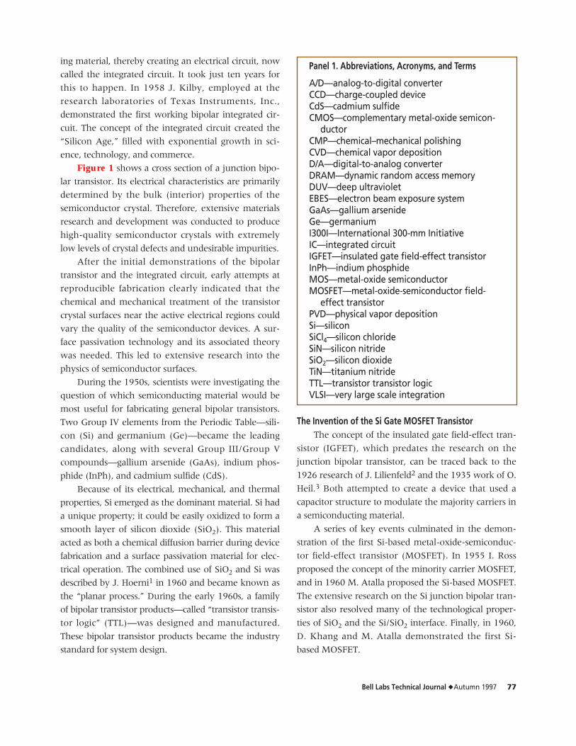
Slowly, but surely, during the past thirty years the
semiconductor industry has migrated from using primar-
ily junction bipolar IC technology to using MOS IC tech-
nology, as illustrated in Figure 7. The bipolar transistor
laid the theoretical and technological foundation for cre-
ating the MOSFET and its many varieties of transistors.
However, the benefits of reduced power consumption,
lowered cost of manufacture per electronic function,
and flexibility of device structure have made Si MOS
the mainstream technology of modern electronics.
The World of VLSIToday, as in the early 1970s, the Si MOS industry
and its related products fall into two major categories:
memory and logic. Each category, in turn, incorpo-
rates major families of products:
• Memory:
– Dynamic random access memory,
– Static random access memory, and
– Nonvolatile random access memory.
• Logic:
– Microprocessors,
– Digital signal processors, and
– Custom logic.
A third minor market segment for VLSI ICs is the
broad class of analog and semi-analog circuits, such as
analog-to-digital converters (A/Ds), digital-to-analog
converters (D/As), and high-speed modems for PC
interfacing to analog telephone networks. The final
segments are niche markets, which incorporate power
devices and high-voltage applications.
The major VLSI technology drivers—DRAMs and
microprocessors—and their applications reside in the
digital arena, because data acquired from our analog
world is immediately converted into digital data that
can be easily computed, compressed, transmitted,
restored, error corrected, and converted back into an
analog signal, if necessary. Modern electronics is a pre-
dominantly binary world, and digital circuits—in the
form of memories and logic—perform all the storage
and computational functions. Prime examples of this
principle range from a wide variety of consumer prod-
ucts, to modern mainframe and personal computers,
and, ultimately, to the digital worldwide telecommu-
nications networks.
The VLSI IC semiconductor industry now exceeds
$150 billion in sales and represents about 17% of the
value included in all electronic equipment sales. To
design, manufacture, and sell in this highly competi-
tive industry, the “clean room” manufacturing facili-
ties must be capitalized on the order of $1.0 billion
increments, as shown in Figure 8.
Mar
ket
shar
e (%
)100
80
60
40
20
01970 1980 1990 2000
Year
BipolarMOS
Figure 7. Market share of ICs by technology.
1960 1970 1980 1990 2000
Co
st (
mill
ion
s o
f d
olla
rs)
$10,000
$1,000
$100
$10
$1
Year of construction
Figure 8. Cost of IC manufacturing clean rooms as a function of time.

84 Bell Labs Technical Journal ◆ Autumn 1997
The PresentThis section reviews the development of the manu-
facturing technology of present day microelectronics,
based on the “planar process.” It describes silicon crystal
technology, crystal dopant techniques, silicon oxidation
development, lithography, materials deposition
processes, pattern transfer mechanisms, metal intercon-
nect technology, and material passivation technology.
IntroductionToday, the manufacture of a leading-edge IC is an
extremely complex procedure, as shown in the sample
VLSI IC in Figure 9, a photomicrograph of a typical
VLSI IC circuit—a modern digital signal processor. The
circuit design and the electrical performance of such
an IC are intimately linked to the technology of IC fab-
rication through the electrical properties of the active
transistors, as well as the parasitic electrical compo-
nents of resistance and capacitance associated with the
materials and processes used to construct the IC. With
respect to the design and manufacture of leading-edge
products, such as DRAMs and microprocessors, an ele-
ment essential to the success of the final IC is the effec-
tive communication process that must take place
between the design and technology research and
development teams.
Today, 0.25-µm CMOS technology is being intro-
duced into manufacture by the major semiconductor
corporations on an international basis. Active develop-
ment is also under way on the next-generation manu-
facturing technology, 0.18-µm CMOS process
technology, scheduled for mass production in the year
2000. Variations of it will be used to fabricate DRAMs
and logic. It is important to understand, however, that
many of the materials and processes used to fabricate
the wide variety of ICs are generic to all types of cir-
cuits, and thereby form the core of a given generation
of technology. The sections that follow describe the
materials and processes that are used to fabricate a
modern IC.
The Planar ProcessAn earlier section of this paper referred to the
“planar process.” Figure 10 illustrates this concept
with a cross section of a modern VLSI IC structure.
The IC structure is fabricated on a silicon crystal
substrate by a process of successive sequences that,
in general:
1. Deposit a specific material or layers of specific
materials,
2. Generate a desired lithographic pattern array on
the Si wafer surface,
3. Perform a transfer process,
4. Remove the lithographic patterning material, and
5. Prepare the surface for the next processing
sequence.
Figure 11 is a photograph of a typical 8-inch-
diameter Si crystal substrate. An array of VLSI ICs is
formed on the wafer. When device fabrication is fin-
ished, the wafer is cut into the individual ICs by a very
thin diamond saw (about 0.003-inch thick). The indi-
vidual working ICs are packaged using a wide variety
of techniques, depending on their final application.
It is customary to outline the VLSI process accord-
ing to the patterning levels in the overall sequence of
fabrication. Table I lists the primary levels being
developed for the 0.18-µm CMOS technology.
Si Crystal TechnologyAll Si VLSI technologies start with the fundamen-
tal material, a silicon crystal. Many excellent refer-
ences relate the history of the development of Si
Figure 9. A modern VLSI circuit—a digital signal processor.

Bell Labs Technical Journal ◆ Autumn 1997 85
crystals used to fabricate ICs.9 Today, the principal
method of growing a large silicon crystal is the
Czochralski technique.10 The process has undergone
continual improvement and refinement, and the
diameters of the crystals have increased steadily over
the years, as shown in Figure 12. The process, how-
ever, remains fundamentally the same.
A small seed crystal of Si is used to draw a single
cylindrical crystal of Si from a quartz crucible filled
with molten Si. The seed crystal is inserted into the
molten silicon and then rotated and slowly withdrawn
from the bath, producing a pure, essentially defect-free
crystal. The rotation and withdrawal rate determine
the diameter of the crystal, and the fracture strength of
the seed crystal ultimately defines its length. This is an
important issue, because as the diameter of the crystal
is increased to improve overall VLSI IC production effi-
ciency, the length of the crystal decreases with the
square of the diameter. This significantly reduces the
total number of wafers produced per crystal.
The molten Si is created from a high-purity poly-
Copper wiring
Via plugs
Aluminum wiring
Tungsten plugs
CMP – Chemical-mechanical polishingHEI – High-energy implantPoly-Si – Polycrystalline siliconSiN – Silicon nitride
Titanium silicide
Recessed isolation oxide
Plasma-deposited silicon nitride
Thin gate oxide
CMP
= 3.0ε
HEI P tub
P substrate
HEI N tub
Si
SiN
Figure 10. Cross section of 0.18-µm VLSI CMOS technology.
Figure 11. A fully fabricated 8-inch Si wafer.

86 Bell Labs Technical Journal ◆ Autumn 1997
crystalline Si charge, produced using a sophisticated
process of chemically reducing silica (sand) into sili-
con. Compounds of silicon are formed—such as silicon
tetrachloride (SiCl4)—and purified through chemical
distillation. The silicon compounds are then reduced to
form the highly pure polycrystalline charges. To main-
tain purity, the polycrystalline Si charge is melted by
induction heating. To eliminate any impurities, the
charge has to be placed in a high-purity SiO2 (fused sil-
ica) crucible. Silicon melts at about 1,415°C, and at
this temperature molten silicon will react with most
materials. As the crystal grows, specific chemical ele-
ments may be added to the silicon melt to achieve the
proper electrical characteristics—n-type or p-type sili-
con. This is called doping the crystal.
The common dopant elements are:
• For p-type silicon: boron, aluminum, gallium,
and indium; and
• For n-type silicon: phosphorus, arsenic, anti-
mony, and bismuth.
In n-type silicon, electrical conduction is associ-
ated with the motion of free electrons; in p-type sili-
con, conduction is associated with “holes,” which are
missing free electrons.
Figure 13 illustrates the process of fabricating
crystals. The silica crucible itself is a primary source of
contamination—oxygen. During the crystal pulling
period, the interior silica surface slowly dissolves,
introducing oxygen into the molten Si bath and the
final crystal. While oxygen is soluble in silicon at very
low levels (about 5.0e1017 atoms per cm3), the oxygen
concentration has to be carefully controlled, not
because it affects the electrical properties of the silicon,
but because it can supersaturate the crystal as it is
being formed, creating internal SiO2 precipitates and
crystal defects.
After the crystal is cooled, it is cylindrically ground
Patterning Descriptionlevel
1 Thin oxide regions
2 Tub regions = p type
3 Tub regions = n type
4 Selective threshold voltage adjust = n channel
5 Selective threshold voltage adjust = p channel
6 Polysilicon doping = n type
7 Polysilicon doping = p type
8 Polysilicon gate definition
9 Lightly doped drain = n-channel transistor
10 Lightly doped drain = p-channel transistor
11 Source/drain doping = n channel
12 Source drain doping = p channel
13 Source/drain contact window
14 Window doping = n type
15 Window doping = p type
16 Metal 1 definition
17 Metal 1—Metal 2 via definition
18 Metal 2 definition
19 Metal 2—Metal 3 via definition
20 Metal 3 definition
21 Metal 3—Metal 4 via definition
22 Metal 4 definition
23 Metal 4—Metal 5 via definition
24 Metal 5 definition
25 Passivation vias
Table I. Photolithographic patterning levels for 0.18-µmCMOS technology.
1950 1960 1970 1980 1990 2000 2010Year
Si w
afer
siz
e (i
nch
es)
14131211109876543210
Actual
Anticipated
Figure 12. Wafer size as a function of time.

Bell Labs Technical Journal ◆ Autumn 1997 87
to specified dimensions, sliced very carefully with a
diamond saw along the desired crystal plane, and
formed into circular wafers. These wafers are then
etched and polished to remove any crystal damage
created by the grinding and slicing processes. Finally,
one side of the wafer undergoes a chemical–mechani-
cal polishing (CMP) process that essentially renders it
atomically smooth. The silicon wafer is then ready for
the “planar process” of forming ICs.
To achieve a desired impurity profile, another sili-
con growth process—called Si epitaxial growth—may be
performed. In this process the Si wafers are heated in a
sealed chamber. Specific gases, such as silane (SiH4),
dichloro-silane (SiH2Cl2), or SiCl4—diluted in a nitro-
gen/hydrogen carrier gas mixture—are passed over
the wafer. Impurity gases—such as phosphine (PH3),
arsine (AsH3), and diborane (B2H6)—may also be
added to determine the impurity level in the growing
layer. By specifically balancing the overall chemical
reaction, a thin layer of precisely doped silicon can be
crystallographically grown on the surface of the sub-
strate silicon wafer, as shown in Figure 14.
Silicon Oxidation TechnologyProbably the most unusual feature of silicon is its
ability to oxidize. The oxidation phenomenon has
been extensively studied and documented by M.
Atalla,11 B. Deal and A. Grove,12 and also by J.
Ligenza.13 Silicon can be oxidized in either dry oxygen
(O2) or pure steam (H2O) over a wide range of gas
pressures and temperatures. Thermal SiO2 can be
grown in very uniform thicknesses, and the growth
process creates an almost atomically smooth interface.
At least forty years of research and technology
Si
Frontopening door
Front openingchamber
Seed holderSeed
Valve
Si
Seal
Argon
Seed shaft
Vacuum pump
Diagnostic port
SiO2 crucible
Graphite crucible
Induction heater
Insulation
Vacuum pumpCrucible shaft
Overall system Interior
Quartz tube
Rotating chuck
Seed crystal
Inductionheating coils
Crucible
Molten silicon
Growing crystalArgon
Figure 13. Growth apparatus for Si crystals.

88 Bell Labs Technical Journal ◆ Autumn 1997
development have enabled manufacturing processes
to grow thermal oxide films with very low defect den-
sity at thicknesses ranging from 2.0 µm (10-6 meters =
1.0 µm) to 2.0 nm (10-9 meters = 1.0 nm.). A 2.0-nm
film is approximately 7 atomic layers thick.
Initially, silicon oxidation proceeds in a linear fash-
ion, with the growth rate determined by the oxidation
reaction rate at the Si/SiO2 interface. As the oxide layer
becomes thicker, the growth rate is controlled by the
diffusion of the oxidizing species through the SiO2, to
the Si/SiO2 interface. After the oxide is grown to its
desired thickness, it can be annealed in either a neutral
gas, such as argon, or chemically active gases, such as
nitrogen or hydrogen. Technologically, a properly
annealed Si/SiO2 interface essentially will be perfectly
atomically matched, chemical bond to chemical bond.
A residual number of excess Si bonds will exist, how-
ever, on the order of 10+9 to 10+10 per cm2. These rep-
resent approximately one unpaired bond for every 10+5
paired bonds. At this low level, transistor characteristics
are no longer influenced, and ideal MOSFET device
characteristics are obtained.
In the early 1980s, E. Poindexter and his cowork-
ers14 performed the definitive work that showed that
active Si interface states consisted of excess Si 2P
orbital bonds, which had three possible electronic
charge states— +1, 0, or -1.
Silicon oxidation incorporates two interesting
mechanisms. First, the oxidation mechanism creates
interstitial, or “free,” Si atoms that diffuse into the Si
crystal. H. Shiraki15 found that if the Si surface oxi-
dizes too rapidly, a large fraction of the Si interstitial
atoms cannot diffuse away from the surface fast
enough and, instead, will aggregate and form crystal
defects. Called stacking faults, these defects can be detri-
mental to final electrical device operation. Later diffu-
sion studies showed that excess silicon interstitial
atoms can also affect dopant diffusion rates by elec-
tronically coupling with the dopants and affecting
their diffusion rates in the silicon crystal.
As the oxidation proceeds, the dissolved oxygen in
the Si crystal diffuses to the continuously restructuring
Si/SiO2 interface and reduces the oxygen concentra-
tion in the top surface of the Si crystal. A denuded zone
is formed, and this can be very beneficial to the quality
of devices formed in the Si surface.
LithographyLithography, a complex process used to produce
an IC pattern, has evolved considerably since the early
1960s. The lithographic process has two major compo-
nents: the production of the masks, which are used to
produce the patterns on the silicon wafer as it is
processed; and the actual technology of printing the
patterns on silicon wafers.
From 1960 to 1970, ICs contained few elements,
making it possible to manually produce a drawing of
each layer used in the fabrication process. The draw-
ing was photographed to produce a master reticule
used in an optical reduction camera to print an array
of each layer on a master glass plate. The master
plate was then reproduced, and production quanti-
ties of masks were made for the wafer fabrication
process. A typical working mask was used from 25
to 50 times. During each printing, the mask was
pressed against the silicon wafer to ensure accurate
pattern reproduction. Because of repeated physical
Si
P
N
P
N
P
Epitaxial Si grown over an Si wafer with a patterned impurity profile,a common process in bipolar technology.
Figure 14. Cross section of epitaxial Si growth on a bipolar Si substrate.
Bell Labs Technical Journal ◆ Autumn 1997 89
contact with the wafer, the mask became so contam-
inated with defects that it had to be discarded.
In the late 1960s, the complexity of ICs grew,
making it exceedingly difficult to manually produce
each master drawing. Clearly, a new technology was
needed. In the early 1970s, D. Herriott led a team of
scientists and engineers who designed and built the
first computer-controlled mask writing machine.16
This machine, known as an electron beam exposure
system (EBES), focused a beam of electrons into a
small circular spot (about 1.0 µm). Using electrostatic
and magnetic deflection lenses, the beam could then
be moved over a surface to an exact location. With
such a machine, it became possible to encode each IC
patterning level in a digital format, store it in a com-
puter format, and then feed the information into EBES
for direct writing of a pattern layer onto the mask
reticule, or the master mask. EBES became an indus-
try standard; it has been extensively refined during the
past twenty-five years, but it still remains the basic
machine for all present-day mask fabrication.
To complete this electron beam technology, new
organic materials were researched and developed.
These materials, which became soluble after exposure
to electron radiation, were named electron beam
resists. Pioneering work in this area was conducted by
L. Thompson and his coworkers at Bell Labs.17
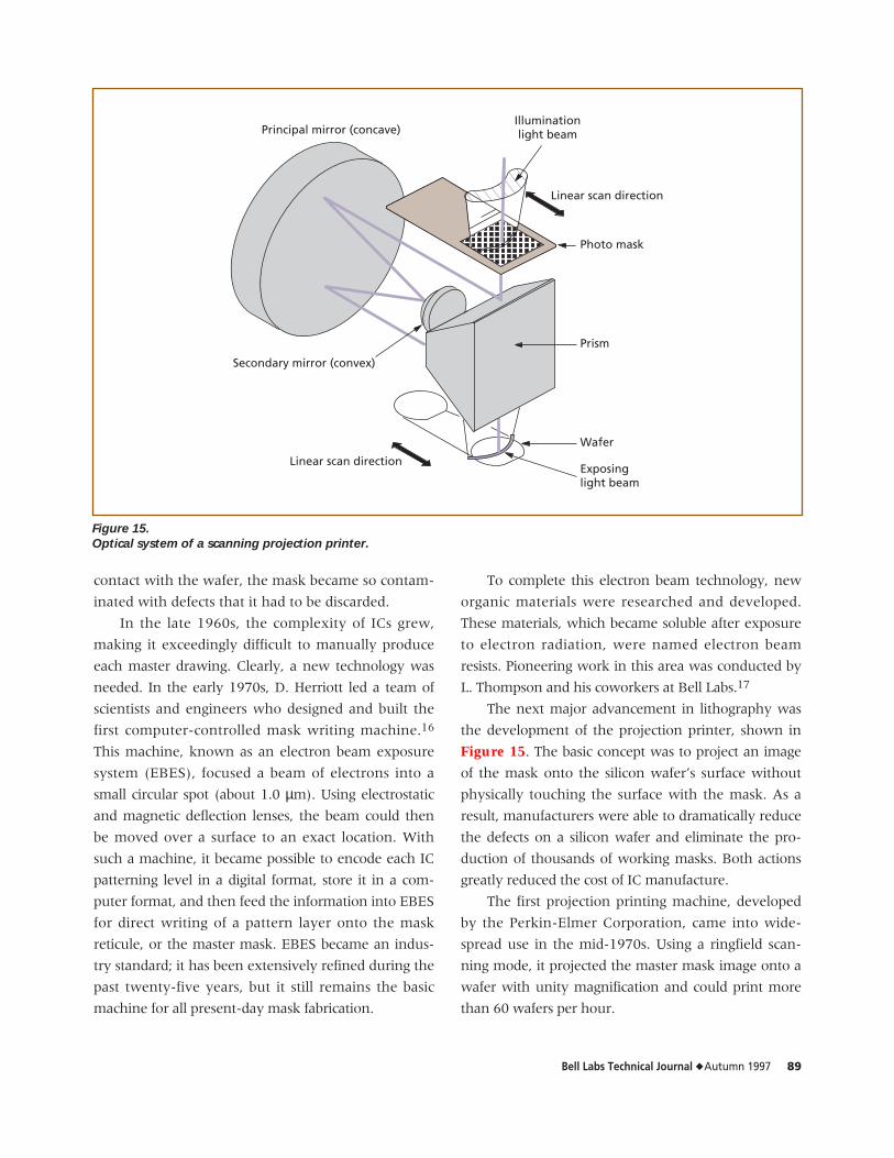
The next major advancement in lithography was
the development of the projection printer, shown in
Figure 15. The basic concept was to project an image
of the mask onto the silicon wafer’s surface without
physically touching the surface with the mask. As a
result, manufacturers were able to dramatically reduce
the defects on a silicon wafer and eliminate the pro-
duction of thousands of working masks. Both actions
greatly reduced the cost of IC manufacture.
The first projection printing machine, developed
by the Perkin-Elmer Corporation, came into wide-
spread use in the mid-1970s. Using a ringfield scan-
ning mode, it projected the master mask image onto a
wafer with unity magnification and could print more
than 60 wafers per hour.
Principal mirror (concave)
Secondary mirror (convex)
Illuminationlight beam
Linear scan direction
Photo mask
Prism
Wafer
Exposinglight beam
Linear scan direction
Figure 15. Optical system of a scanning projection printer.

90 Bell Labs Technical Journal ◆ Autumn 1997
By 1980, Perkin-Elmer dominated the litho-
graphic exposure tool industry. However, another
“killer” technology was being introduced. The GCA
Corporation had also developed a projection machine.
The new machine was a “step and repeat” tool that
projected the image of the master reticule directly onto
the wafer. The critical element in the stepper was a
high-quality refractory lens with 5X reduction. As
steppers became the new industry standard, they were
manufactured by several major corporations, including
GCA, Nikon, Canon, and Ultratech.
In partnership with Perkin-Elmer, IBM
researchers developed the next-generation tool, which
combined stepping and scanning. Modern versions of
the step and scan system are now manufactured by
several major corporations, including SVGL, Nikon,
and Canon.
Advances in lithography resolution were made in
various ways. In addition to mechanical and optical
improvements in the printing machines, the photosen-
sitive emulsions that were applied to the wafer for the
initial imaging were extensively improved. At first,
materials were borrowed from the newspaper printing
industry, but they lacked the resolution needed for IC
features. The research and development of photoresist
materials became an international technical issue. The
chemistries involved, which are extremely complex,
are described in detail by W. M. Moreau.18
The third area of improvement in lithography was
research and development in the wavelength (λ) of
the exposing light. To manufacture silicon wafers in
high volume, it was convenient for the exposing
wavelength to be in the ultraviolet range. High-pres-
sure, high-intensity mercury light sources were avail-
able, and the lithography industry concentrated its
research and development efforts at the “G-line”
(λ = 432 nm) of the mercury light spectrum. This
approach was viable, but researchers began to explore
submicron dimensions for fabricating MOSFETs
(L > 1.0 µm). Using G-line light, basic optical theory
limits printing resolution to about 0.50 µm. In the
early 1990s, to print 0.35-µm feature sizes, the lithog-
raphy industry was required to make an intermediate
shift in exposure wavelength to the “i-line” of mercury
light (λ = 365 nm).
In the early 1980s, however, a team of researchers
at Bell Labs designed and built the first deep ultraviolet
(DUV) optical stepper, using a krypton fluoride laser as
the light source (λ = 248 nm). Today, DUV step and
scan tools and associated photoresist materials are
emerging as the production lithography process for
0.25-µm IC technology.
Advances in optical lens materials, optical imaging
techniques, mechanical tool design, and organic pho-
toresist materials are now required to emerge as
rapidly as all other aspects of the IC technology.
Exposure systems and resist materials based on argon
fluoride laser illumination (λ = 193 nm) are now
under active research and development for the manu-
facture of 0.18-µm CMOS technology.
Materials Deposition TechnologyDuring the fabrication of an IC, many process
steps require the deposition of specific materials, from
metals to insulators. Their deposition must be uni-
formly controlled in chemical composition, mechani-
cal properties, thickness, and defect level over the
entire wafer.
The deposition processes fall into two major
classes: the chemical vapor deposition (CVD) technique
and the physical vapor deposition (PVD) technique.
Each class subdivides into subclasses that require partic-
ular deposition methods for each material.
In the major field of CVD, a chemical reaction
takes place during the deposition. Reactant compo-
nents, in a gas phase, are brought together in a reactor,
and the reaction usually proceeds in a heterogeneous
manner. In a heterogeneous gas reaction, the active
compounds react selectively on the surface of the
wafer, and, possibly, on the interior surfaces of the
reactor chamber. A homogenous gas reaction is
avoided, because it leads to particle buildup in the gas
phase and, ultimately, to deposition of these particles
on the surface of the wafer. During subsequent process
steps, these particles will become defect sites and
severely limit the IC yield. Many CVD processes are
thermally activated, and the chemical reactions need
to be carefully characterized to ensure that the process
is optimized.
Another type of CVD process is performed via
plasma deposition chemistry. This process creates a gas

Bell Labs Technical Journal ◆ Autumn 1997 91
plasma, such as nitrogen or argon, into which reactant
gases are introduced. After the gas molecules are ion-
ized and fractionated into various radicals, the reaction
(recombination of radicals) occurs on the wafer sur-
face and, possibly, on the chamber walls. The reactions
and subsequent materials properties depend on the
wafer temperature and the plasma (including such
dependent variables as plasma density, radio-
frequency power, DC bias, and chamber geometry).
An important consideration of CVD processes and
the materials deposition is the degree of uniformity, or
conformal coverage, that is achieved on the silicon wafer
surface during deposition, as shown in Figure 16.
CVD processes are carefully characterized with respect
to molecular surface mobility, the resultant degree of
conformal coverage, and the mechanical stress resi-
dent in the deposited films. If the film stress is highly
tensile, films will crack after a given thickness is
deposited. On the other hand, if the stress is highly
compressive, the deposited film can delaminate from
the silicon wafer surface. Typical materials that can be
deposited by CVD for IC fabrication include polycrys-
talline and/or amorphous silicon, silicon dioxide
(SiO2), glasses (phosphosilicate and borosilicate), sili-
con nitride (Si3N4), titanium nitride (TiN), tungsten
(W), and aluminum (Al).
In the major field of PVD materials processing,
deposition involves physically moving the mater-
ial from a source and depositing it uniformly on
the wafer surface. One of the earliest examples of
PVD processes was the evaporation of metal films.
Typically, a metal charge of aluminum was heated
in a vacuum chamber, and the evaporated alu-
minum coated the entire wafer surface. The meth-
ods of heating the aluminum were electron guns,
induction heating, and filament evaporation.
The electron gun system is no longer used,
because the x-rays it created caused chemical bond
breaking in SiO2 and electrical damage to the active
device structures. An important discovery arose, how-
ever, from the use of electron guns. In this system, the
aluminum charge resided in a water-cooled copper
holder. As the aluminum evaporated, the copper
slowly alloyed with the molten aluminum during
deposition and was incorporated into the deposited
aluminum film, creating a copper concentration of
about 0.4%. Technologists discovered that aluminum
deposited in this fashion was much more reliable than
pure aluminum. Today, aluminum alloys containing
0.4% copper are still routinely used.
The old PVD systems have now been almost com-
pletely replaced by plasma sputter deposition systems.
In these systems, a small plasma of argon or nitrogen is
created near the material source. The gas ions hit the
target and vaporize the material by molecular collision.
Proper engineering of the targets and the vacuum sys-
tem geometry enable the final material to be uni-
formly deposited on the silicon wafer.
PVD has one potential disadvantage. The
deposited material usually does not have enough
energy and surface mobility to uniformly cover a steep
topology. In modern CMOS technology, device struc-
tures may have aspect ratios on the order of 2 to 1.
The non-uniform coverage of materials can lead to
failures in manufacturing or, in the worst case,
decreased reliability. Typical problems associated with
PVD processes are incomplete material coverage of
steep walls, as shown in Figure 17, and failure to act
as a continuous materials and/or barrier layer.
SiO2
Si
Nonconformal coverage
SiO2
Si
Conformal coverage
Figure 16. Conformal and nonconformal step coverage.

92 Bell Labs Technical Journal ◆ Autumn 1997
Pattern Transfer from Photoresist Material into DeviceMaterials
In the process of fabricating ICs, the pattern is
transferred to the materials on the silicon wafer by
etching, as shown in Figure 18. Initially, ICs had
rather large horizontal dimensions—on the order of
10.0 µm—and the films to be etched were on the
order of 0.50 µm, as shown at the top of Figure 18. A
wet chemistry technique, which has many beneficial
aspects, was used to perform the early patterning. The
etchant chemicals can be produced with extremely
high purity, interact with the specific material on the
silicon wafer at the atomic level via a chemical reac-
tion, and consequently show very minor geometrical
effects or residual contamination. Chemicals such as
phosphoric acid, hydrofluoric acid, hydrochloric acid,
nitric acid, and potassium hydroxide were and are still
commonly used in modern silicon processing. Because
of environmental concerns, many of these chemicals
are either recycled or neutralized for safe disposal.
Using wet chemicals for pattern transfer has a
major drawback, however. The wet chemicals will
etch the material in an isotropic manner (see Figure
18), undercutting the masking material. With present
lithographic geometries on the order of 0.35 µm,
isotropic undercutting will completely eliminate the
pattern. Feature size control became a major issue in
the 3.5-µm VLSI technology, and researchers began
working on methods to eliminate the undercut.
At the same time, scientists were conducting
research on using plasmas to etch materials. Their
major goal was to eliminate the inconveniences that
extensive wet chemistry brought to the manufactur-
ing facility. In one of the first applications of plasma
etching, scientists used oxygen plasma to strip organic
photoresist layers from silicon wafers. At that time,
most wet strippers contained biphenyl compounds,
which were found to be carcinogenic. Technologists
found that by adding certain chlorinated or fluori-
nated chemicals to the etching plasma, they could
achieve an anisotropic etching effect, as shown at the
bottom of Figure 18. Analysis indicated that deposit-
ing etchant byproducts on the sidewalls of the feature
edges as the material was being etched inhibited lat-
eral etching. The solution to vertical pattern transfer
had been discovered. For each material to be etched,
technologists had to develop a specific chemistry and
a set of plasma operating conditions. However, com-
plex plasma etching enabled IC technologists to con-
SiO2
Si
Potentialfailure points
Figure 17. Poor materials step coverage by a PVD process.
EtchingThe process of removing material—such as oxide orother thin films—by chemicals, electrolytes, or plasmaion bombardment.
Isotropic etch
An etch that proceeds laterally and down at equalrates. Wet chemical etches are generally isotropic innature.
An etch that has very little lateral activity. Most of theetching occurs in the vertical direction. Dry etch systemsare primarily anisotropic.
Window formedby developing photoresist
Undercut
Noundercut
Anisotropic etch
Photoresist
Film
Substrate
Photoresist
Film
Substrate
Photoresist
Film
Substrate
Figure 18. Pattern transfer.

Bell Labs Technical Journal ◆ Autumn 1997 93
tinue to reduce the horizontal dimensions.
The general field of plasma etching contains three
distinct regions, each associated with a plasma density
and an ion excitation energy:
• In the high-density gas region of plasma etch-
ing (p > 100 millitorr, where p stands for pres-
sure), etching occurs by chemical reaction;
• In the medium-density gas region, called reac-
tive ion etching (p ~ 10 millitorr), etching occurs
by combining physical bombardment and
chemical reaction; and
• In the low-density gas region, known as
sputtering (p < 1 millitorr), physical bombard-
ment is the dominant mechanism for remov-
ing material.
Within each major area, there are significant vari-
ations in the reactor designs, the plasma configuration,
and the electrical biasing conditions.
Plasma etching, however, did have significant
technical issues associated with it. The etching byprod-
ucts proved to be extremely corrosive, and vacuum
pumping technology required major advances.
Furthermore, discharge gases had to be neutralized
using “scrubbers” that removed environmentally dam-
aging gases, such as chlorine and fluorine, which cause
the “ozone depletion effect.”
With respect to the processed wafers, another
technical issue began to arise as the submicron regime
was researched and developed. Plasma etching with
reactive ions was electrically damaging the thin SiO2
insulator materials that comprise the ICs. This area is
now under extensive study; and as device geometries
and material film thicknesses continue to be scaled
downward, the plasma damage problem is a major
issue that needs to be addressed at each plasma pro-
cessing step.
Incorporating Dopant into the Si WaferTo achieve the desired electrical device structure,
dopants must be selectively introduced into the crystal
surface, in specific regions, to create the required dopant
profiles as a VLSI IC is being fabricated. Figure 19
shows the three major methods that have been used
extensively during the evolution of manufacturing
processes for discrete transistors and VLSI ICs.
To some degree, all three methods use another
unique property of SiO2, which was first reported by
C. Frosh and L. Derick in 1957 and extensively
researched later. They discovered that the primary
dopant elements for silicon processing diffused very
slowly through thin layers of SiO2. This property was
crucial to the “planar process.” Basically, a thin layer of
SiO2 could be grown on the silicon wafer surface, and
then the desired pattern could be etched through the
SiO2 using either hydrofluoric acid or plasma etching
to expose the regions to be doped.
In the first technique, the surface of the wafer was
exposed to a gas of the desired dopant. Depending on
the temperature of the process, the gas would dissoci-
ate and the dopant element would diffuse into the Si,
but not through the SiO2. This technique, shown in
Figure 19a, was first used in fabricational processes
where the concentration control is critical, as in the
diffused base junction of a bipolar device.
The second technique is based on solid-state dop-
(a) Gas phase doping
Dopant atomSiO2
Si substrateDiffused region
(b) Solid-state doping
Dopant glassSiO2
Si substrateDiffused region
Phosphosilicateglass
(c) Ion implantation
Ionized dopant atomSiO2 LayerSi substrateImplanted dopant profile
Figure 19. Doping techniques for Si crystals.

94 Bell Labs Technical Journal ◆ Autumn 1997
ing from a glass source, shown in Figure 19b. This
technique introduces the dopant into a furnace gas
stream, along with an oxidizing ambient, causing a
glass to grow on the surface of the silicon wafer, which
then acts as the diffusion source. It is used primarily
for creating diffusions where the surface concentration
should equal the solid solubility of the impurity in sili-
con, such as in junction bipolar emitters and MOSFET
source/drains diffusions. The second technique is also
used to dope polycrystalline layers, found in the gate
structures of MOSFETs and the capacitor structures of
DRAM cells. After the diffusion is completed, the dop-
ing glass source is removed from the silicon wafer sur-
face with a hydrofluoric acid or a nitric acid solution.
Figure 19c shows the third dopant technique,
called ion implantation, which came into widespread
use in the mid-1970s. First a gas containing the
dopant atoms is ionized, and then the ions are passed
through a mass spectrometer, creating a high-purity
ion beam. The beam is then accelerated to a specific
energy, and the ions are implanted into the surface of
the wafer. The three most common materials used to
mask the regions of the wafer that are not being
doped are SiO2, polysilicon, and photoresist. Ion
implantation, illustrated in Figure 20, offers device
technologists many degrees of freedom in the forma-
tion of dopant profiles in the silicon surface. It can
accurately set not only the energy (and depth) of the
dopant profile, but also the dose. By measuring the
current that flows into the wafer, it is possible to
make a precise count of the dopant ions.
Today, ion implantation is used for almost all dop-
ing processes in which total dose can be accurately
controlled over a range of 10+10 to 10+17 ions per cm2.
At least four technical issues must be carefully con-
trolled in ion implantation. First, ions can build a
charge layer in the various materials on the wafer sur-
face and cause insulator breakdown. To resolve this
problem, the wafers are exposed to electron flood guns
that neutralize the wafer during implantation. Second,
Ion source
Ion accelerator
Vacuum pump
Mass separationmagnet
Beam sweepingelectrodes
Multiple wafertarget chamber forbatch production
Rotary drive
Currentintegrator
Vacuumpump
Ion beam
Figure 20. Principle components of an ion implantation machine.

Bell Labs Technical Journal ◆ Autumn 1997 95
the high-energy beam can also erode atoms off the
internal surfaces of the implant machine and intro-
duce undesired impurities into the silicon wafer. To
control this problem, critical parts of the machine are
made from silicon. Third, high-energy ions can create
significant silicon crystal damage, which can alter the
desired dopant profiles and also degrade device perfor-
mance. Fourth, high-dose, high-energy production
machines can cause significant wafer heating, which in
turn can distort the wafers. Combating this effect
requires adequate wafer cooling techniques.
Metallization TechnologyThe processes described in the previous sections
are used to fabricate an IC’s individual transistors,
resistors, and capacitors. To form the desired IC, pat-
terned thin-metallic films connect the individual bipo-
lars, MOSFETs, resistors, capacitors, and diodes.
In the early years of discrete transistors, bipolar
ICs, and MOSFET ICs, metallurgists explored a variety
of metallization systems. Metals such as silver, gold,
platinum, palladium, tungsten, and aluminum were
popular choices. By the mid-1970s, however, almost
all manufacturers found that an aluminum-copper
alloy (Cu = 0.4 to 4.0 atomic percent) was the most
practical material to use. It was an excellent conductor,
easy to deposit and pattern, and it satisfied the reliabil-
ity requirements for use in ICs.
Until the mid-1980s, a single layer of aluminum
metallization was used to fabricate most ICs. It was
then realized that using only one layer of metal
severely limited the planar layout of the IC and the
number of active devices per unit area. Researchers
quickly substituted multiple layers of metal. The IBM
Corporation was a clear leader in this field. Today,
modern ICs at the 0.35-µm feature size typically con-
tain as many as four to five layers of metal. While the
processing associated with this multilayer metallization
is complex, it is cost effective overall, because the size
of the IC can be significantly reduced and its perfor-
mance greatly improved.
As the feature sizes of modern ICs have
decreased, the vertical walls and aspect ratios of con-
tacts between the various metal layers and the silicon
substrate have made the formation of reliable contacts
more difficult. During the past several years, the use
of tungsten, conformly deposited by CVD, has helped
to solve this problem.
There are still, however, several major issues asso-
ciated with the use of aluminum metallization. First,
the aluminum conductors on an IC are subjected to
extremely high current densities. For example, typical
circuit design guidelines will specify current densities
on the order of about 3.0x10+5 amps/cm2. The current
density is a factor of 10+3 higher than current densities
encountered in household wiring, creating a condition
whereby the momentum of the conducting electrons
is transferred to the aluminum atoms in the film, caus-
ing them to physically move. This phenomenon, called
electromigration, has been researched extensively for
the past thirty years.
Second, deposited aluminum films are usually
under tensile stress, either as a result of the initial
deposition conditions or the thermal cycling conditions
experienced in operation. If the stress becomes exces-
sive, the finely patterned lines will plastically deform
and, in the worst case, void, creating what is known as
Si – SiliconSiO2 – Silicon dioxideTi – TitaniumTiN – Titanium nitrideTiSi2 – Titanium silicide
Low K dielectric
Tungsten
TiN
Ti
Silicon
SiO2
Si
TiSi2
Diffusion
Aluminum
Figure 21. Detailed cross section of a modern multilayer metalstructure.

96 Bell Labs Technical Journal ◆ Autumn 1997
stress migration. The separation in the aluminum line
will cause the IC to fail. To avoid this type of failure in
modern ICs with submicron feature sizes, the alu-
minum lines are sandwiched between conducting
films of titanium nitride (TiN), as shown in Figure 21.
The use of multilayer metallization structures has
raised a third issue, feature definition. As the metal
layers cross each other and are separated by an insula-
tor, a severe topology is generated on the wafer sur-
face. The variation in surface height can exceed 1.0
µm and, in this condition, modern lithography cannot
print the required feature sizes.
Technologists have presented two basic solutions to
this problem. In the first solution, a thick layer of
organic material is applied to the wafer surface after the
intermediate insulators have been deposited. This
material smoothes the surface to a large degree, but not
completely. The organic material and part of the under-
lying insulator are then plasma etched, producing a
fairly smooth surface, as shown in Figure 22. The etch
rate of the organic polymer and the insulator must be
equal for this process to work well. In some cases, geo-
metrical effects associated with the organic material
limit the ability to produce a truly planar surface.
The second process uses the technique that origi-
nally produced the flat silicon wafer, which involves
polishing the intermediate insulator covering the
wafer surface to achieve a high degree of planarity.
This technique seems to contradict a general rule for
handling wafers: Never touch the active surface of the
wafer during fabrication. However, the existing exper-
tise in polishing slurries, polishing pads, and cleaning
techniques has made CMP the leading process used to
produce planar multilayer metallization systems in
modern VLSI ICs.
Device PassivationDevice passivation is another important field of IC
processing and reliability. Passivation materials are
introduced in semiconductor manufacture to ensure
the initial fabricational yield, electrical performance,
and extended reliability of the IC.
After the metallization process is completed, the
silicon wafer is ready to be cut into individual ICs and
packaged. The silicon wafer is covered with a thick
layer of insulating material, usually an SiO2 glass that
contains phosphorus or a plasma-deposited silicon
nitride material (SiN). Commonly used variations in
the passivation layer result in layered structures, or
compounds, referred to as silicon oxynitrides (an
amorphous tertiary material that contains varying
amounts of silicon, oxygen, and nitrogen). Initially,
the passivation layer protects the IC from mechanical
damage during initial circuit testing and the sawing
and packaging operations. After the IC is packaged and
tested, the passivation layer continues to protect it
from the undesired effects of ionic contamination in
the packaging compounds.
SiO2 has another unique property. Although it is
an excellent diffusion barrier to the dopants used in
Dielectric
Organic polymer
Polysilicon
Substrate
Wafer preparation
Plasma flux
Plasma etch in process,etching polymer and dielectric
at same rate
Etch-back complete
Figure 22. Organic polymer planarization etch-back process.

Bell Labs Technical Journal ◆ Autumn 1997 97
the manufacturing process, SiO2 can be easily contam-
inated with alkali ions such as lithium, sodium, potas-
sium, and cesium. The diffusion rate of these materials
in SiO2 decreases rapidly with the mass of the ion.
Sodium, an element found everywhere on the surface
of the earth, is the ion most likely to degrade the oper-
ation of discrete bipolars, discrete MOSFETs, and ICs.
In the operational temperature range of semiconduc-
tor devices (typically, -40°C to 100°C), sodium diffuses
rapidly through SiO2, making sodium diffusion barri-
ers and sodium “getters” necessary for ensuring high
electrical parameter yields and long-term device relia-
bility in the IC manufacturing process. (A getter is a
chemical or a process that absorbs and neutralizes an
impurity.)
In 1964 D. Kerr of IBM made a major break-
through in passivation.19 Kerr left the phosphorus
glass used in a bipolar process on the final silicon
wafer. When submitted to reliability aging, the pack-
aged bipolar devices he was fabricating demonstrated
exceptionally stable operation. This discovery led to
the extensive characterization of the phosphosilicate
glass system. Since then, other sodium diffusion barri-
ers have been developed, most notably silicon nitride,
by J. Dalton in 1966. The combination of these two
materials forms the basis of all passivation technology
in today’s VLSI ICs.
Present Manufacturing FacilitiesDuring the past thirty years, the manufacture of
VLSI ICs has grown exponentially. The need to meet
the electrical performance demands (such as clock fre-
quency and power consumption) of system designers
and the quantities of VLSI ICs required in the market-
place has forced the manufacturing technology, as
described in the earlier sections, to evolve rapidly.
Processes have become quite complex, and the wafer
size continues to increase. IC manufacturing has trans-
formed itself from a labor-intensive industry to a capital-
intensive industry. Today, a modern, competitive
manufacturing facility costs in excess of $1.0 billion to
construct. About 20% of a facility’s cost goes into the
construction of the clean room, including the support
facilities of water purification and recycling, air purifi-
cation with temperature/humidity control, and all
other aspects of the infrastructure. The remaining 80%
is allocated for the manufacturing equipment. The cost
estimates of modern manufacturing equipment are:
• Lithography exposure tools—about $7 million
each,
• Plasma processing machines—about $2 million
each, and
• Furnaces and ancillary equipment—about $1.0
million each.
To ensure that manufacturing plants are managed
efficiently, considerations such as operations
research—including wafer queuing theory, opera-
tional equipment efficiency, wafer process times,
inventory control, and overall cost of ownership
analysis—are now as important as the purity of the
chemicals and the silicon wafers that are used in the
facility. The modern facility is a fascinating blend of
advances in leading-edge technology and economic
management theory. Given that the lifetime of most
IC technologies for leading-edge product manufacture
is only three to five years, factories must also be flexi-
ble enough to be quickly upgraded to accommodate
several generations of manufacturing technology.
In conjunction with these financial issues, the
industry has by necessity entered a “post-yield-limiting
era.” No longer is VLSI IC yield predicted by defect
density theory and dominated by defects. With such
enormous capital investments, each fabricational
process has been engineered to virtually eliminate
defects. Modern DRAM and microprocessor manufac-
turing plants have wafer yields (number of wafers fin-
ished/number of wafers started) in excess of 95% and
IC yields (number of working ICs per wafer/number of
potential ICs per wafer) in excess of 90%.
The FutureToday’s microelectronics industry faces major
technical and economic issues. This section discusses
the paths that the industry may take in these areas.
IntroductionAt present, 0.25-µm VLSI CMOS technology is
being introduced into manufacture for the produc-
tion of 64-Mb (64e10+6) DRAMs and advanced
microprocessors, and 0.18-µm VLSI CMOS technol-
ogy is under advanced development, scheduled for
introduction to manufacture in the year 2000. The

98 Bell Labs Technical Journal ◆ Autumn 1997
major technical issues of these generations of VLSI
CMOS have been largely resolved. The financial
issues associated with implementing these technolo-
gies, however, will represent a significant challenge
for most IC manufacturers.
The next-generation technology, 0.13-µm VLSI
CMOS, is in the advanced stages of research, and the
fundamental issues facing a 0.10-µm VLSI CMOS
technology are in the early research phase. Major
technical issues concerning these generations of tech-
nology need to be resolved, foremost among which
are lithography, metallization, gate dielectrics, and
electrical parameter control. And, finally, financial
issues may be the fundamental limiting factor for
introducing advanced technologies.
LithographyLithography is the fundamental technology for the
mass manufacture of ICs. If IC technology is to con-
tinue to scale in feature size, it will require major
advances in lithography. This issue is being addressed
by research and development activities taking place in
several major fields.
In the field of optical lithography, exposure wave-
length is a fundamental limiting parameter for the reso-
lution of minimum feature size. Evolutionary optical
lithography research and development in the wave-
length region of 193 nm (argon fluoride lasers) should
yield optical systems that will allow the continued scal-
ing and production of ICs with a minimum feature size
of about 0.15 µm. Because light, with a wavelength of
about 0.15 µm, is strongly absorbed by almost all mate-
rials, future optical lithographic imaging systems with
such short wavelengths will need to be constructed
using reflective mirrors, rather than the refracting lenses
used today.
Lithographic research efforts in the area of
extreme ultraviolet light, with wavelengths of 50 nm
to ~10 nm, have used mirror technology. Research
currently being conducted at λ = 13 nm uses mirrors
based on the Bragg reflection principle. These mirrors
are constructed from the super lattices of materials—
layers of alternating high- and low-density materials
whose thickness must be critically controlled.
Because Bragg mirrors are extremely difficult to
manufacture, imaging system design and routine
mirror fabrication have not yet been used in any
extensive commercial application. Furthermore, the
mask technology used with them must also be reflec-
tive, and the resist systems must be surface based,
owing to the highly absorbing nature of all materials
in this wavelength region.
In another approach, X-rays with a wavelength of
about 1.0 nm are being explored in a unity-printing
mode, because neither a lens nor a mirror technology
exists. In this mode, the critical technology is masking,
since the mask substrate must be a thin membrane—
about 100 nm thick—to remain essentially transparent
to the exposing X-rays. The IC features are formed on
this membrane in a strongly absorbing material, such
as a low-stress tungsten or a tantalum alloy. To mini-
mize diffraction effects during exposure, the mask
must be placed very close—about 5.0 µm—to the sur-
face of the Si wafer. Producing high-quality, defect-
free masks with no physical distortion is extremely
difficult and has yet to be demonstrated as an efficient
manufacturing technology.
Although attempts have been made to use ion
beams in lithography, fundamental physical effects
have limited all approaches. No method has been dis-
covered to achieve cost-effective throughput for a low-
intensity ion beam exposure system. On the other
hand, if the ion beam is high in intensity, the ion-ion
interaction leads to unacceptable image blurring and
reduced resolution.
Electron beam technology—an established tech-
nology for mask making and IC research activities—
presents a very promising lithographic approach.
However, the current reticule production systems,
which use a finely focused electron beam to write
each pixel, are too slow for practical IC production
use. Only projection electron beam systems offer a
potential throughput that is cost effective. Scientists
are conducting research and development on several
variations of electron beam projection technology. A
critical feature of each of these systems is the mask-
ing technology. Initial attempts at projection elec-
tron beam lithography—using either a fixed or
variable aperture concept to construct an image
from a series of rectangles and triangles—to date
have not yielded a throughput that is cost effective.
Bell Labs Technical Journal ◆ Autumn 1997 99
More recently, research into an advanced, cost-
effective system called Scalpel™, which uses a fixed
mask and a unique scattering technique to define
the electron beam pattern, is very promising for fea-
ture sizes smaller than 0.15 µm.20
In general, the physics, chemistry, and technology
of electron beam lithography have been well estab-
lished. But the critical technical issues concerning
residual pattern placement errors and cost-effective
wafer fabrication will need to be continually addressed
until a truly high-volume, sub 0.15-µm lithography
system can be introduced into manufacturing facilities.
MetallizationThe technology of metallization now represents
more than half of the process of Si wafer fabrication.
This is a result of the exponentially increasing num-
ber of transistors and logic blocks, and the need to
interconnect them. At present, four to five metal lay-
ers are being used on new VLSI designs in 0.25-µm
CMOS technology.
As feature sizes continue to decrease, current den-
sity and parasitic capacitance are becoming major
issues in determining overall circuit performance.
Higher limits of current density are needed in power
distribution lines, clock signal lines, and data buses. As
a result, research and development into material sys-
tems, such as copper—with lower resistivity and better
electromigration resistance than aluminum—is now
very active.
Also, as the size of metallization spaces continues
to shrink, the parasitic capacitances between lines are
dramatically increasing. The response to this issue is
research and development of insulators with reduced
dielectric constants, as compared to SiO2 (k = 3.9). A
first generation of fluorinated SiOF compounds is
being developed with k = 3.5, and longer-term
research into organic polymers with k = 2.0 to 2.5
appears promising.
Gate DielectricsThe scaling of all feature sizes, both in the lateral
and vertical dimensions, has now led us to the point
where fundamental considerations, such as quantum
mechanics, are factors critical to further scaling. As
SiO2 layers about the thickness of 2.0 nm are used in
research and development, significant gate insulator
tunneling currents are observed in MOSFETs. While
these currents may not pose a significant issue to cir-
cuit design or reliability, they can severely limit low-
power applications of future VLSI CMOS, many of
which are in portable, battery-operated applications.
It may be necessary, therefore, to replace SiO2
as the gate dielectric and use a high-dielectric mate-
rial, such as tantalum pentoxide, Ta2O5 (k ≈ 24), or
titanium dioxide, TiO2 (k ≈ 100). The quantum
mechanical tunneling currents are suppressed by
the thicker film, and the higher dielectric constant
allows the gate electrode to continue to control the
transistor action.
Electrical Parameter ControlContinued technology scaling increases the sig-
nificance of fundamental limitations in transistor
parameter control. As the MOSFET continues to
shrink, the total number of active dopant atoms
under a given gate decreases. Statistical theory indi-
cates that, with present crystal preparation tech-
niques, random fluctuations in doping density will
seriously affect MOSFET device parameter control.
Such an effect can virtually stop device scaling,
because many designs, such as DRAMs, require pre-
cisely matched transistors within sense amplifier cir-
cuits that measure the small amounts of charge
stored in each memory cell.
Financial IssuesIf the costs of new manufacturing equipment con-
tinue to rise, they can severely limit the introduction
of new technological advances, creating an effect simi-
lar to one that exists in the airline industry.
Technologically, airplanes can routinely fly faster than
the speed of sound; however, because of the financial
and technical complexity issues associated with super-
sonic flight, the airline industry has instead adopted
the concept of the jumbo jet and mass passenger trans-
port. In a similar way, VLSI ICs may evolve into fully
integrated, complete electronic systems on a single cir-
cuit. This will reduce overall system cost and improve
total electrical performance without further dramatic
reductions in feature dimension. Several major corpo-
rations recently announced that they plan to integrate
a number of IC products into a single VLSI IC. Such an
IC will be fabricated with a modular type of VLSI tech-

100 Bell Labs Technical Journal ◆ Autumn 1997
nology and will include large logic blocks; memory in
the range of 10e+6, or higher; and analog functions.
Pessimists have argued repeatedly that the IC
industry would slow its progress in technology, but to
date, it has not. The industry has reached the financial
point that manufacturing plant construction is
exceedingly costly. Consequently, many smaller cor-
porations have adopted joint ventures between and
among themselves as a workable solution, or else
they rely on huge VLSI Si foundry corporations for
their product manufacture.
Another aspect of VLSI IC economics is that
national standards of living are becoming dependent
on microelectronics manufacturing capability. On the
national level, governments are subsidizing microelec-
tronics research and development and the building of
VLSI IC manufacturing plants to improve the eco-
nomic prospects of their countries. But if the cost of
research and development and manufacturing facili-
ties in the microelectronics industry continues to
climb at an exponential rate, as it has in the past, only
international cooperation will keep these costs afford-
able. There are already indications that such a possi-
bility may evolve.
In the area of advanced semiconductor research
and development, organizations such as SEMATECH,
initially a U.S. government/industry consortium, have
already engaged the active participation of foreign cor-
porations. Also, in the area of research and develop-
ment for the manufacture of 300-mm (12-inch)
silicon wafers, the subsidiary formed by SEMATECH,
called International 300-mm Initiative (I300I), has
recently agreed to work with the SELETE Consortium
of Japan to share technical information to develop a
common set of material and equipment standards.
These actions indicate that R&D costs (and the associ-
ated technical risks) are becoming too burdensome for
any individual corporation or national consortium of
corporations to handle. In addition, the semiconductor
equipment manufacturers will only be able to eco-
nomically survive if they can sell to a global market
with an international set of standards.
Social and financial issues, not technical issues,
may ultimately limit the widespread application of
advanced deep submicron 0.10-µm VLSI IC technol-
ogy. The social revolution of the early 1990s finds its
roots in national financial collapse and restructuring
primarily caused by unchecked technological competi-
tion in the military fields.
ConclusionThe historical revolution in microelectronics—
from the first step of the invention of electrical ampli-
fication in a single semiconducting device in 1948, to
present day VLSI IC technology, in which ~5e10+8
transistors exist on a single piece of semiconductor
crystal—is completely unparalleled in any other tech-
nology in the history of mankind. The science, tech-
nology, and financial issues confronting the VLSI
industry are international in scope, and its technical
future is very difficult to predict. The “killer” technol-
ogy for VLSI ICs has not been identified. Technically,
scientists have demonstrated quantum-level device
structures that would further reduce the size of a
device capable of performing a logic or memory oper-
ation, but they have yet to seriously address the tech-
nological and financial aspects of fabrication and
volume production. The future of microelectronics
will be the most interesting story to unfold in the next
two decades.
References1. J. A. Hoerni, “Planar Silicon Transistors and
Diodes,” IRE Trans. on Electron Devices, Vol. ED-8,No. 2, Mar. 1961, p. 178.
2. J. E. Lilienfeld, “Method and Apparatus forControlling Electric Currents,” U.S. Patent1,745,175, filed Oct. 8, 1926, issued Jan. 28, 1930.
3. O. Heil, “Improvements in or Relating toElectrical Amplifiers and Other ControlArrangements and Devices,” British Patent439,457, filed Mar. 4, 1935, issued Dec. 6, 1935.
4. R. E. Kerwin, D. L. Klein, and J. C. Sarace, “Methodfor Making MIS Structures,” U.S. Patent 3,475,234,filed Mar. 27, 1967, issued Oct. 28, 1969.
5. B. T. Murphy, “Cost Size Optima of MonolithicIntegrated Circuits,” Proc. Inst. Electr. Eng., Vol. 52, 1964, pp. 1537–1545.
6. R. H. Dennard, F. H. Gaensslen, H-N. Yu, V. L. Rideout, E. Bassous, and A. R. LeBlanc,“Design of ion-implanted MOSFET’s with verysmall physical dimensions,” IEEE J. Solid-StateCircuits, Vol. SC-9, No. 5, Oct. 1974, pp. 256–268.
7. G. E. Moore, “Progress in digital integrated elec-tronics,” Technical Digest of the 1975 Intl. Electron

Bell Labs Technical Journal ◆ Autumn 1997 101
Devices Meeting, IEEE, Washington, D.C., Dec. 1–3, 1975, pp. 11–13.
8. G. E. Moore, “VLSI: Some FundamentalChallenges,” IEEE Spectrum, Vol. 16, No. 4, Apr. 1979, pp. 30–37.
9. Martin Grayson, ed., Encyclopedia of SemiconductorTechnology, John Wiley, New York, 1984.
10. G. K. Teal, “Single crystals of germanium andsilicon—basic to the transistor and integratedcircuit,” IEEE Trans. Electron Devices, Vol. ED-23,No. 7, July 1976, pp. 621–639.
11. M. Atalla, E. Tannenbaum, and E. J. Scheibner,“Stabilization of Silicon Surfaces by ThermallyGrown Oxides,” Bell System Technical Journal,Vol. 38, No. 3, May 1959, pp. 749–783.
12. B. Deal and A. Grove, “General Relationship forthe Thermal Oxidation of Silicon,” J. AppliedPhysics, Vol. 36, No. 12, Dec. 1965, pp. 3770–3778.
13. J. Ligenza, “Oxidation of Silicon by High-Pressure Steam,” J. Electrochem. Soc., Vol. 109,No. 2, Feb. 1962, pp. 73–76.
14. P. J. Caplan, E. Poindexter, B. Deal, and R. Razouk, “ESR centers, interface states, andoxide fixed charge in thermally oxidized siliconwafers,” J. Applied Physics, Vol. 50, No. 9, Sept. 1979, pp. 5847–5854.
15. H. Shiraki, “Elimination of stacking faults in sili-con wafers by HCl added dry O2 oxidation,”Japanese J. Appl. Physics, Vol. 14, No. 6, June 1975,pp. 747–752.
16. D. R. Herriott, R. J. Collier, D. S. Alles, and J. W. Stafford, “A practical electron lithographicsystem,” IEEE Trans. Electron Devices, Vol. ED-22,No. 7, July 1975, pp. 385–392.
17. L. F. Thompson, C. G. Willson, andM. J. Bowden, eds., Introduction to Micro-lithography, ACS Symposium Series 219,American Chemical Society, Washington, D.C.,1983.
18. Wayne M. Moreau, Semiconductor Lithography,Plenum Press, New York, 1988.
19. D. Kerr, J. Logan, P. Burkhardt, andW. Pliskin, “Stabilization of SiO2 PassivationLayers with P2O5,” IBM J. Research and Develop-ment, Vol. 8, No. 4, Sept. 1964, pp. 376–384.
20. S. D. Berger and J. M. Gibson, “New approachto projection-electron lithography with demon-strated 0.1 µm linewidth,” Appl. Phys. Lett., Vol. 57, No. 2, July 9, 1990, pp. 153–155.
Further ReadingThe references below, background information for
the development of the transistor, are listed according
to their dates of publication.– Adi J. Khambata, Introduction to Integrated Semicon-
ductor Circuits, John Wiley, New York, 1963.– Edward Keonjian, ed., Microelectronics Theory,
Design and Fabrication, McGraw-Hill, New York,1963.
– Raymond M. Warner, Jr., ed., IntegratedCircuits—Design Principles and Fabrication,McGraw-Hill, New York, 1965.
– A. Many, Y. Goldstein and N. B. Grover,Semiconductor Surfaces, North-Holland,Amsterdam, 1965.
– A. S. Grove, Physics and Technology of SemiconductorDevices, John Wiley, New York, 1967.
– E. Kooi, The Surface Properties of Oxidized Silicon,Springer-Verlag, New York, 1967.
– R. M. Burger and R. P. Donovan, eds., Funda-mentals of Silicon Integrated Device Technology, 2 vols., Prentice-Hall, Englewood, N. J., 1967.
– S. M. Sze, Physics of Semiconductor Devices, John Wiley, New York, 1st ed., 1969.
– William M. Penney and Lillian Lan, eds., MOSIntegrated Circuits, Van Nostrand Reinhold, New York, 1972.
– Richard S. Muller and Theodore I. Kamins,Device Electronics for Integrated Circuits, John Wiley, New York, 1977.
– Arthur B. Glaser and Gerald E. Subak-Sharpe,Integrated Circuit Engineering—Design, Fabricationand Applications, Addison-Wesley, Reading,Mass., 1977.
– George R. Brewer, ed., Electron Beam Technologyin Microelectronic Fabrication, Academic Press,New York, 1980.
– S. M. Sze, Physics of Semiconductor Devices, John Wiley, New York, 2nd ed., 1981.
– E. H. Nicollian and J. R. Brews, MOS Physics andTechnology, John Wiley, New York, 1982.
– S. P. Murarka, Silicides for VLSI Applications,Academic Press, New York, 1983.
– S. M. Sze, VLSI Technology, McGraw-Hill, New York, 1st ed, 1983.
– Gerard Barbottin, ed., Instabilities in SiliconDevices—Silicon Passivation and Related Instabilities,North-Holland, Amsterdam, New York, 1986.
– S. Wolf and R. N. Tauber, Process Technology, Vol. 1 of Silicon Processing for the VLSI Era, Lattice Press, Sunset Beach, Calif.,1986.
– J. V. McCanny and J. C. White, eds., VLSITechnology and Design, Academic Press, Londonand New York, 1987.
– Wayne M. Moreau, Semiconductor Lithography—Principles, Practices and Materials, Plenum Press,New York, 1988.
– Billy L. Crowder, ed., Ion Implantation inSemiconductors and Other Materials, Plenum Press,New York, 1988.

102 Bell Labs Technical Journal ◆ Autumn 1997
– S. M. Sze, VLSI Technology, McGraw-Hill, New York, 2nd ed, 1988.
– G. Fry, J. Griffin, D. Potter, R. Bowman, and R. Skinner, Practical VLSI Fabrication for the ‘90s,Integrated Circuit Engineering Corporation,Scottsdale, Arizona, 1990.
– S. Wolf, Process Integration, Vol. 2 of SiliconProcessing for the VLSI Era, Lattice Press, Sunset Beach, Calif., 1990.
– Richard D. Skinner, ed., Basic Integrated CircuitTechnology Reference Manual, Integrated CircuitEngineering Corporation, Scottsdale, Arizona,1993.
– Kwok K. Ng, Complete Guide to SemiconductorDevices, McGraw-Hill, New York, 1994.
– L. Peters, J. Griffin and R. Skinner, eds., CostEffective IC Manufacturing, Integrated CircuitEngineering Corporation, Scottsdale, Arizona,1995.
– R. Bowman, J. Giffin, D. Potter, and R. Skinner,eds., Advanced VLSI Fabrication, IntegratedCircuit Engineering Corporation, Scottsdale,Arizona, 1995.
– S. Wolf, The Submicron MOSFET, Vol. 3 of SiliconProcessing for the VLSI Era, Lattice Press, SunsetBeach, Calif.,1995.
(Manuscript approved November 1997)
JAMES T. CLEMENS, head of the VLSI ResearchDepartment at Bell Labs in Murray Hill, New Jersey, earned a B.S. in physics and aPh.D. in theoretical physics from PolytechnicInstitute of New York in New York City. Hedirects research and development of silicon-
based VLSI integrated circuits and is also the technicalprogram manager for the Lucent–NEC joint researchand development alliance, which was named a gold-level winner of the 1997 Bell Labs President’s Award.Dr. Clemens is a Fellow of the Institute of Electrical andElectronics Engineers and serves as the Meetings Chairfor the IEEE Electron Device Society and as the ExecutiveChair of the IEEE/Japanese Society of Applied PhysicsInternational Symposia on VLSI Technology andCircuits. In 1994, Dr. Clemens was awarded the ClintonJ. Davisson trophy for his highly valuable patent onepitaxial Si structures. ◆