Embed Size (px)
Citation preview
Laser Photonics Rev. 6, No. 1, 47–73 (2012) / DOI 10.1002/lpor.201100017
LASER & PHOTONICSREVIEWS
Abstract An overview is presented of the current state-of-the-art in silicon nanophotonic ring resonators. Basic theory of ringresonators is discussed, and applied to the peculiarities of sub-micron silicon photonic wire waveguides: the small dimensionsand tight bend radii, sensitivity to perturbations and the boundaryconditions of the fabrication processes. Theory is compared toquantitative measurements. Finally, several of the more promis-ing applications of silicon ring resonators are discussed: filtersand optical delay lines, label-free biosensors, and active ringsfor efficient modulators and even light sources.
Silicon microring resonatorsWim Bogaerts*, Peter De Heyn, Thomas Van Vaerenbergh, Katrien De Vos, Shankar KumarSelvaraja, Tom Claes, Pieter Dumon, Peter Bienstman, Dries Van Thourhout, and Roel Baets
1. Introduction
Silicon photonics has become one of the most promisingphotonic integration platforms in the last years. This can bemainly attributed to the combination of a very high indexcontrast and the availability of CMOS fabrication technol-ogy [1], which allows the use of electronics fabricationfacilities to make photonic circuitry [1–5]. Passive siliconwaveguide structures have shown an unprecedented reduc-tion in footprint of waveguides, and especially wavelength-selective devices [6,7]. Ring resonators are a prime exampleof this. In addition, over the past years there have been manydemonstrations of integrated active devices including modu-lators [2, 8, 9], Germanium-based photodetectors and evenIII-V integrated sources and detectors [10–13].
Ring resonators play an important role in the success ofsilicon photonics, because silicon enables ring resonators ofan unprecedented small size. A generic ring resonator con-sists of an optical waveguide which is looped back on itself,such that a resonance occurs when the optical path lengthof the resonator is exactly a whole number of wavelengths.Ring resonators therefore support multiple resonances, andthe spacing between these resonances, the free spectralrange (FSR), depends on the resonator length. As we willdiscuss in Sect. 4, for many applications it is preferred tohave a relatively large FSR (several nm), and this impliesthe use of small rings. This translates into a very hard re-quirement for the optical waveguide: to make a compactring, a small bend radius is required, and this in turn is onlypossible with high-contrast waveguides with strong confine-ment. Some examples of Silicon ring resonators are shownin Fig. 3.
Because of the very high refractive index contrast be-tween silicon and its oxide (or air), single-mode strip wave-guides (so-called photonic wires) can have bend radii below5 μm. This allows for extremely compact rings, even withan FSR over 20 nm at telecom wavelengths around 1550 nm.This is in stark contrast with lower contrast material systemswhere rings need to be much larger.
A ring resonator as a stand-alone device only becomesuseful when there is a coupling to the outside world. Themost common coupling mechanism is using codirectionalevanescent coupling between the ring and an adjacent buswaveguide. As will be discussed in more detail in the nextsection, the transmission spectrum of the bus waveguidewith a single ring resonator will show dips around the ringresonances. This way, the ring resonator behaves as a spec-tral filter, which can be used for applications in opticalcommunication, especially wavelength division multiplex-ing (WDM). Alternatively, these ring spectra can by usedfor sensing: as we will discuss in Sect. 2.5, the position andthe shape of the resonance dips are very sensitive to a varietyof effects, which can be detrimental (stability of a filter) oradvantageous (as a sensor, or for tuning). We will discusssome applications in Sect. 4.
In this paper we will give an overview of the field ofsilicon microring resonators. We will start with a brief theo-retical discussion of general ring resonator properties, andexpand that to explore the parameters that might influencea silicon microring: this will indeed show that the use ofhigh-contrast silicon comes with benefits, but also with sig-nificant drawbacks with respect to tolerances. To illustratethe various effects we show measurements in our own lab.
Photonics Research Group, Ghent University – imec, Department of Information Technology* Corresponding author: e-mail: [email protected]
© 2011 by WILEY-VCH Verlag GmbH & Co. KGaA, Weinheim
48
LASER & PHOTONICSREVIEWS
W. Bogaerts et al.: Silicon microring resonators
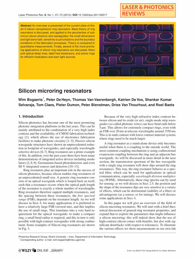
Figure 1 Examples of silicon ring resonators. (a) Double ringresonator with tuned directional coupling sections, (b) Circular ringwith large coupler gaps, (c) Ultra-small racetrack ring with 1 μmbend radius, (d) ring with conformal coupling sections, (e) Largefolded-spiral ring.
However, in many cases similar results were obtained byother groups. Finally, we discuss possible applications ofring resonators, with a focus on optical delay lines, biosen-sors and active rings.
2. Properties of a ring resonator
Before going into detail into the specifics of silicon micror-ing resonators, we first discuss the generic properties of ringresonators. This will help us to further understand the uniquepossibilities, as well as the limitations of silicon microrings.
Optical microresonators are extensively described inliterature [6, 14, 15]. In general a ring resonator consistsof a looped optical waveguide and a coupling mechanismto access the loop. When the waves in the loop build up around trip phase shift that equals an integer times 2π , thewaves interfere constructively and the cavity is in resonance.
In what follows, we will briefly summarize all concepts andformulas that are needed to describe the functional behaviorof ring resonators.
2.1. All-pass ring resonators
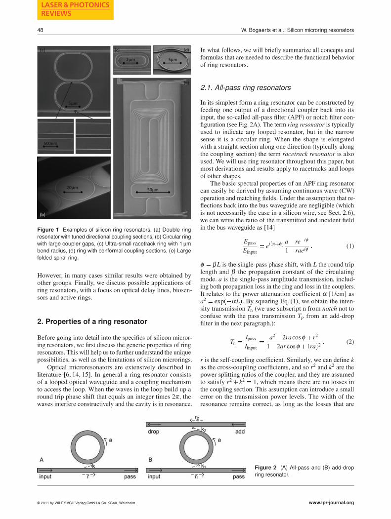
In its simplest form a ring resonator can be constructed byfeeding one output of a directional coupler back into itsinput, the so-called all-pass filter (APF) or notch filter con-figuration (see Fig. 2A). The term ring resonator is typicallyused to indicate any looped resonator, but in the narrowsense it is a circular ring. When the shape is elongatedwith a straight section along one direction (typically alongthe coupling section) the term racetrack resonator is alsoused. We will use ring resonator throughout this paper, butmost derivations and results apply to racetracks and loopsof other shapes.
The basic spectral properties of an APF ring resonatorcan easily be derived by assuming continuous wave (CW)operation and matching fields. Under the assumption that re-flections back into the bus waveguide are negligible (whichis not necessarily the case in a silicon wire, see Sect. 2.6),we can write the ratio of the transmitted and incident fieldin the bus waveguide as [14]
Epass
Einput� ei�π�φ� a� re�iφ
1� raeiφ � (1)
φ � βL is the single-pass phase shift, with L the round triplength and β the propagation constant of the circulatingmode. a is the single-pass amplitude transmission, includ-ing both propagation loss in the ring and loss in the couplers.It relates to the power attenuation coefficient α [1/cm] asa2 � exp��αL�. By squaring Eq. (1), we obtain the inten-sity transmission Tn (we use subscript n from notch not toconfuse with the pass transmission Tp from an add-dropfilter in the next paragraph.):
Tn �IpassIinput
�a2�2racosφ � r2
1�2ar cosφ ��ra�2� (2)
r is the self-coupling coefficient. Similarly, we can define kas the cross-coupling coefficients, and so r2 and k2 are thepower splitting ratios of the coupler, and they are assumedto satisfy r2� k2 � 1, which means there are no losses inthe coupling section. This assumption can introduce a smallerror on the transmission power levels. The width of theresonance remains correct, as long as the losses that are
Figure 2 (A) All-pass and (B) add-dropring resonator.
© 2011 by WILEY-VCH Verlag GmbH & Co. KGaA, Weinheim www.lpr-journal.org
Laser Photonics Rev. 6, No. 1 (2012)
REVIEWARTICLE
49
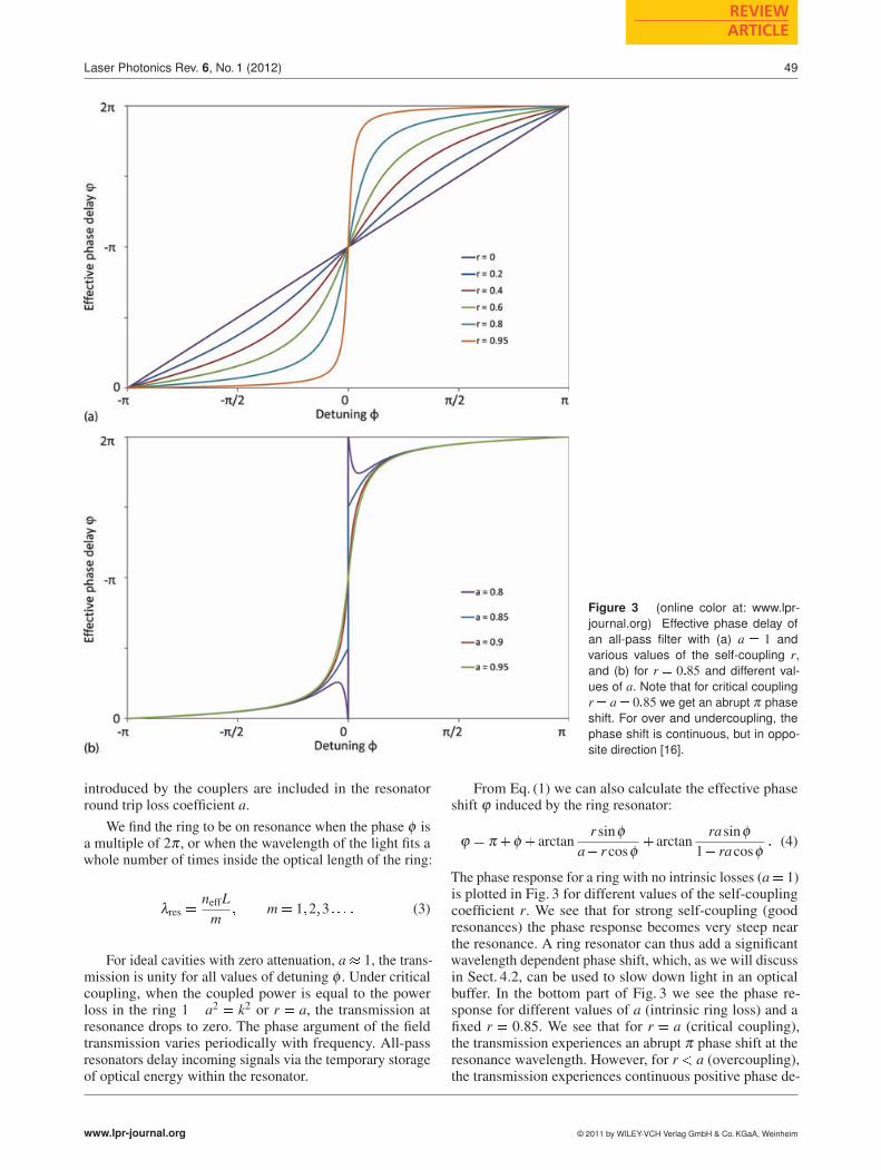
Figure 3 (online color at: www.lpr-journal.org) Effective phase delay ofan all-pass filter with (a) a � 1 andvarious values of the self-coupling r,and (b) for r � 0�85 and different val-ues of a. Note that for critical couplingr � a� 0�85 we get an abrupt π phaseshift. For over and undercoupling, thephase shift is continuous, but in oppo-site direction [16].
introduced by the couplers are included in the resonatorround trip loss coefficient a.
We find the ring to be on resonance when the phase φ isa multiple of 2π , or when the wavelength of the light fits awhole number of times inside the optical length of the ring:
λres �neffL
m� m� 1�2�3 � � � � (3)
For ideal cavities with zero attenuation, a� 1, the trans-mission is unity for all values of detuning φ . Under criticalcoupling, when the coupled power is equal to the powerloss in the ring 1� a2 � k2 or r � a, the transmission atresonance drops to zero. The phase argument of the fieldtransmission varies periodically with frequency. All-passresonators delay incoming signals via the temporary storageof optical energy within the resonator.
From Eq. (1) we can also calculate the effective phaseshift ϕ induced by the ring resonator:
ϕ � π�φ � arctanr sinφ
a� r cosφ� arctan
rasinφ1� racosφ
� (4)
The phase response for a ring with no intrinsic losses (a� 1)is plotted in Fig. 3 for different values of the self-couplingcoefficient r. We see that for strong self-coupling (goodresonances) the phase response becomes very steep nearthe resonance. A ring resonator can thus add a significantwavelength dependent phase shift, which, as we will discussin Sect. 4.2, can be used to slow down light in an opticalbuffer. In the bottom part of Fig. 3 we see the phase re-sponse for different values of a (intrinsic ring loss) and afixed r � 0�85. We see that for r � a (critical coupling),the transmission experiences an abrupt π phase shift at theresonance wavelength. However, for r � a (overcoupling),the transmission experiences continuous positive phase de-
www.lpr-journal.org © 2011 by WILEY-VCH Verlag GmbH & Co. KGaA, Weinheim
50
LASER & PHOTONICSREVIEWS
W. Bogaerts et al.: Silicon microring resonators
lay, while for r � a (undercoupling) the phase shift near theresonance shows a strong decrease, which is plotted as a 2πphase shift in Fig. 3b [16].
2.2. Add-drop ring resonators
When the ring resonator is coupled to two waveguides, theincident field is partly transmitted to the drop port (seeFig. 2B). The transmission to the pass and the drop port canalso be derived from CW operation and matching the fields.
Tp �IpassIinput
�r22a2�2r1r2acosφ � r21
1�2r1r2acosφ ��r1r2a�2� (5)
Td �IdropIinput
��1� r21��1� r22�a
1�2r1r2acosφ ��r1r2a�2� (6)
If the attenuation is negligible (a � 1), critical couplingoccurs at symmetric coupling (k1=k2). For a lossy resonator,critical coupling occurs when the losses match the couplingas r2a � r1.
2.3. Spectral characteristics
The characteristic parameters are indicated in Fig. 4. Theydepend on the losses and coupling coefficients and can beextracted directly from the formulas for transmission (2), (5),and (6). The results are listed below. In Sect. 3.3 we willperform the reverse operation: starting from the measuredspectral characteristics, the losses and coupling coefficientsof SOI ring resonators will be determined.
From expressions (2), (5), and (6) we can derive the fullwidth at half maximum (FWHM) of the resonance spectrumfor an all-pass ring resonator:
FWHM��1� ra�λ 2
res
πngL�
ra� (7)
and for an add-drop ring resonator configuration:
FWHM��1� r1r2a�λ 2
res
πngL�
r1r2a� (8)
Within a first order approximation of the dispersion, thewavelength range between two resonances or free spectralrange (FSR) in function of wavelength equals:
FSR�λ 2
ngL(9)
with L the round trip length. The strong confinement in SOIwires allows for very sharp bends (radius down to 3 μm)with still low radiation. This largely increases the potentialFSR of SOI ring resonators as compared to conventionaloptical resonators.
Note that in both FWHM and FSR we find the groupindex in the denominator, not the effective index neff. Thegroup index takes into account the dispersion of the wave-guide and is defined by
ng � neff�λ0dneffdλ
� (10)
The group index, and the corresponding group velocityvg �
cng, describes the velocity at which the envelope of
a propagating pulse travels and is a characteristic of a dis-persive medium (or waveguide).
The on-off extinction ratio of the through port transmis-
sion is equal to TtRmin
. For an APF ring configuration, we get
for Tt and Rmin:
Tt ��r�a�2
�1� ra�2� (11)
Rmin ��r�a�2
�1� ra�2� (12)
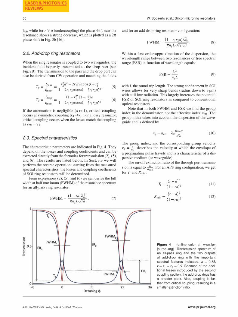
Figure 4 (online color at: www.lpr-journal.org) Transmission spectrum ofan all-pass ring and the two outputsof add-drop ring with the importantspectral features indicated. a � 0�85,r � r1 � r2 � 0�9. Because of the addi-tional losses introduced by the secondcoupling section, the add-drop rings hasa broader peak. Also, coupling is fur-ther from critical coupling, resulting in asmaller extinction ratio.
© 2011 by WILEY-VCH Verlag GmbH & Co. KGaA, Weinheim www.lpr-journal.org
Laser Photonics Rev. 6, No. 1 (2012)
REVIEWARTICLE
51
For an add-drop configuration, we can define the same ERTmaxTd
for the drop transmission. At resonance, the ER be-
tween through and drop port of an add-drop resonator is
given by TmaxRmin
. Tt , Rmin, Tmax and Td are defined as:
Tt ��r2a� r1�2
�1� r1r2a�2� (13)
Rmin �r22a2�2r1r2a� r21
�1� r1r2a�2� (14)
Tmax ��1� r21��1� r22�a
�1� r1r2a�2� (15)
Td ��1� r21��1� r22�a
�1� r1r2a�2� (16)
The finesse is defined as the ratio of FSR and resonancewidth,
Finesse�FSR
FWHM� (17)
It is thus a measure of the sharpness of resonances relativeto their spacing. The quality factor (Q-factor) is a measureof the sharpness of the resonance relative to its central fre-quency,
Q-factor�λres
FWHM� (18)
The physical meaning of the finesse and Q-factor re-lates to the number of round-trips made by the energy inthe resonator before being lost to internal loss and the buswaveguides. This is a temporal phenomenon and must be ex-amined with the transient response. The mathematics are de-scribed in numerous text books and publications [14,17,18].The finesse is found to represent within a factor of 2π thenumber of round-trips made by light in the ring before itsenergy is reduced to 1/e of its initial value. The Q-factorrepresents the number of oscillations of the field before thecirculating energy is depleted to 1/e of the initial energy.To define the Q-factor, the microring is excited to a certainlevel and the rate of power decay is considered. From thispoint of view it is understood that round trip losses as wellas coupling in the directional couplers are loss factors thatneed to be reduced to obtain high-Q resonances. Thereforean all-pass resonator will exhibit a higher Q-factor thanan add-drop resonator (when both devices operate close tocritical coupling).
We make a distinction between loaded Q and unloadedQ. The unloaded Q of a resonator is the Q-factor whenthe resonator would not be coupled to waveguides. Whencoupling to a waveguide, additional losses are introduced tothe cavity. Hence, the loaded Q is always smaller than theunloaded Q. We always mean loaded Q when referring toQ-factor, unless it is specifically mentioned otherwise.
2.4. Losses and coupling
As we will discuss in more detail when covering siliconrings, we can separate the losses into different contributions:
waveguide propagation losses and losses in the couplingsection. When we discuss a racetrack resonator, instead of aring, we can add excess bend losses due to mismatch lossesat the straight-bend transition. Losses in the coupling sectionoriginate from propagation losses, from additional sidewallroughness affecting the distributed intensity, and even froma mismatch in waveguide width caused by the fabricationprocess (see Sect. 3.1).
The roundtrip loss A includes the three loss contributorssummarized above:
A�dB� � A�
propagationL�2Acoupler�4Abend � (19)
with A�
propagation the propagation loss per unit of length, typ-
ically expressed in [dB/cm]. From Eq. (18) and (17) theQ-factor and finesse can be rewritten as a function of thephysical parameters of an all-pass ring resonator:
Q-factor�πngL
�ra
λres�1� ra�� (20)
Finesse�π�
ra1� ra
� (21)
and for an add-drop ring resonator:
Q-factor�πngL
�r1r2a
λres�1� r1r2a�� (22)
Finesse�π�r1r2a1� r1r2a
� (23)
In order to increase the Q-factor, it is crucial to reduce thelosses in the cavity. Propagation losses are diminished byhigh quality SOI material and high quality processing [19].Bend losses might be reduced by design of adiabatic bendsthat curve smoothly instead of circular bends [20].
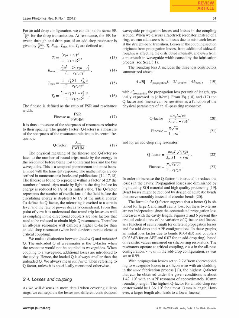
The formula for Q-factor suggests that a better Q is ob-tained for large L and small cavity loss, but these two termsare not independent since the accumulated propagation lossincreases with the cavity length. Figures 5 and 6 present the-oretical calculations of the variation of Q-factor and finesseas a function of cavity length for different propagation lossesand for add-drop and APF configurations. In these graphs,an initial loss factor due to bends (0.04 dB) and couplers(0.035 dB for an APF and 0.07 for an add-drop ring), basedon realistic values measured on silicon ring resonators. Theresonators operate at critical coupling, r = a in the all-passconfiguration, r1=r2a in the add-drop configuration. r2 wasset to 0.99.
With propagation losses set to 2.7 dB/cm (correspond-ing to waveguide losses in a silicon wire with air claddingin the imec fabrication process [1]), the highest Q-factorthat can be obtained under the given conditions is about1�42 �105 with an APF resonator of approximately 10mmroundtrip length. The highest Q-factor for an add-drop res-onator would be 1�36 �105 for almost 13mm in length. How-ever, a larger length also leads to a lower finesse.
www.lpr-journal.org © 2011 by WILEY-VCH Verlag GmbH & Co. KGaA, Weinheim

52
LASER & PHOTONICSREVIEWS
W. Bogaerts et al.: Silicon microring resonators
Figure 5 (online color at: www.lpr-journal.org) Quality factor as afunction of cavity length for four propagation loss figures.
Figure 6 (online color at: www.lpr-journal.org) Finesse as afunction of cavity length for four propagation loss figures.
2.5. Sensitivity
The resonance of the ring resonator depends on the opticalroundtrip length of the ring, and the losses accumulated(all loss mechanisms combined, including coupling to buswaveguides). Therefore, ring resonators will be sensitive toa multitude of effects. that is why they are also attractivefor use in sensing applications (see Sect. 4.3). We definesensitivity as the amount of wavelength shift Δλres causedby a certain amount of whatever effect we are studying,be it temperature, physical deformation or compositionalchanges of the waveguide core or cladding. A shift of theresonance wavelength λres is essentially caused by a changeof the effective index of the resonant mode neff. Based onEq. (3), we get
Δλres �ΔneffL
m�m � 1�2�3 � � � (24)
where m is the order of the resonant mode. neff is influencedby the refractive index of the cladding, which is altered uponsensing. As we will see in the next section, in submicronsilicon waveguides, the waveguide dispersion can not beneglected. A change of neff will primarily alter λres, which
in turn will influence neff due to the non-zero slope of∂neff∂λ .
In a first order approximation both effects can be decoupled:
Δλres �
��∂neff∂nenv
�λres�n0env
Δnenv��
∂neff∂λ
�λres�n0env
Δλres
�� L
m
With n0eff at the initial resonance wavelength. After sub-stitution in formulas (3) and (10) at λ � λres, a compactformula for the resonance wavelength shift with first orderdispersion will appear:
Δλres �Δenvneff � λres
ng(25)
where Δenvneff is the effective index shift caused by an envi-
ronmental change, Δenvneff ��
∂neff∂nenv
�λres�n0env
Δnenv.
From the variational theorem of waveguides, Δenvneffcaused by a local change of dielectric constant Δε�x�y�, canbe expressed as [21–23]
Δenvneff � c�
ΔεEv � E�
vdxdy (26)
where Ev�x�y� is the normalized modal electric field vectorof the waveguide mode in the ring.
The ring response scales with the squared amplitudeof the electric field at the perturbation and, therefore, withthe fraction of the total modal power contained in the sur-face volume where the dielectric constant is modified. Thisfraction can be increased by changing the waveguide coredimension, and thus changing the confinement in any part ofthe core or cladding. A rigorous derivation of the sensitivityof neff of slab waveguides for variations of the environmentwas performed by Tiefenthaler et al. in [22].
2.6. Counterdirectional coupling
Each mode of a microring resonator can travel in two direc-tions, the forward propagating mode, which is intentionallyexcited by the bus waveguide, and the backward propagatingmode. Counterdirectional (or contra-directional) coupling isthe mutual coupling between these two modes. When thereis coupling, this will result in a net power transfer from theforward (deliberately excited) mode to the backward propa-gating mode, and this coupling also causes distortion to theideal Lorentzian-shaped spectrum by resonance-splitting.To understand resonance-splitting due to counterdirectionalcoupling, we describe this system in temporal coupled-modetheory (TCMT) [18, 24, 25].
Consider an ideal resonator (e. g. circular symmetric,with perfect sidewall smoothness and without a couplingsection), where the forward and backward traveling-wavemodes are uncoupled, frequency-degenerate eigenmodes ofthe system. However, in practice, small perturbation which
© 2011 by WILEY-VCH Verlag GmbH & Co. KGaA, Weinheim www.lpr-journal.org
Laser Photonics Rev. 6, No. 1 (2012)
REVIEWARTICLE
53
can be felt by the optical mode can break this symmetry andcouple the two traveling-wave modes. The traveling wavesare then no longer uncoupled. However, the system will havetwo new eigenmodes (linear combinations of the originaltravelling-wave eigenmodes) which are uncoupled. In thecase of a single point-like perturbation in the ring, such asthe coupling section, the new eigenmodes are pure standing-wave modes, symmetric (a�) and antisymmetric (a
�
) w. r.to the perturbation [18]. Forward propagating light in thewaveguide will then excite the symmetric and antisymmetricmode 90� out of phase. Due to symmetry breaking, theseuncoupled eigenmodes are no longer degenerate, resultingin a resonance frequency shift and thus the spectrum willshow resonance-splitting.
In principle, this perturbation could be induced by thepresence of a bus waveguide [24], since the two standingwaves will feel a slightly different environment (effectiverefractive index) causing the supermodes to resonate on aslightly different frequency. From the traveling-wave view-point, the directional coupler is then a periodically phase-matched scatterer into the backward propagation direction,thus building up the power in the counterpropagating modeand splitting the supermodes. A good introduction aboutthe modelling of the back-reflection caused by the cou-pling section can be found in [26]. Also sidewall-roughness-induced backscattering has been predicted [27] and demon-strated [25, 28] to lead to deleterious resonance splitting.
As we will see in Sect. 3, in silicon waveguides the im-pact of the bus waveguide will rather be small in comparisonwith the impact of sidewall corrugation, such that the for-mer effect can be ignored. However, in higher-order filters,with several coupling sections, it might limit designers toobtain a good extinction ratio. A solution has been proposedin [24] by choosing for a longer and weaker directional cou-pler that covers several propagation wavelengths of the ringmode, thus reducing the difference in environment betweenthe modes.
Little et al. show in [27] that if the time to deplete thering due to counterdirectional coupling becomes smallerthan the time to charge up the ring to its steady-state value,resonance-splitting becomes visible in the spectrum of theresonator. This behavior is usually translated into R � k2with R the mutual coupling between the forward and back-ward propagating mode and k the external coupling. Be-cause it is often desirable to keep k low to achieve a narrowline width, even minor reflections will cause problems inhigh-Q devices.
Next to resonance-splitting, counterdirectional couplingalso causes power reflecting back into the input waveguideand/or the add-port. These reflections are usually referred toas surface-roughness induced backreflection which is com-mon present in any high-index-contrast waveguide designand can accurately be quantified by inverse Fourier trans-forming the spectrum [29]. This backreflection is stronglyenhanced by the resonances of the ring and increases withthe groups index of the ring [30].
Even for a single given ring, the resonance splitting canstrongly vary between different resonance wavelengths [31].Following the arguments in [27], the depth of the sidewall
corrugation is mostly considered as a stochastic variable,corresponding with a gaussian correlation function witha fixed variance and correlation length. Both the varianceand correlation length are determined by the fabricationprocess. The randomness of the roughness induces the un-predictability of the backscattering level at the differentresonance wavelengths.
Recently it was experimentally demonstrated thatbackscattering is indeed a wavelength dependent randomprocess whose statistics is independent of the shape, size,refractive index contrast, and technology of the wave-guide [32]. However, it has been reported [33] that whenresonators are fabricated with electron beam lithography,the surface-roughness can be semi-periodic, as it could con-sist of a group of ridges which have similar amplitude andperiod. In such case the roughness is better modeled asa quasi-grating. This reduces the unpredictability of thebackscattering at a certain wavelength, as the backscatteringlevel now becomes a determenistic function of the wave-length. It is expected that controlling the shape of the quasi-gratings in the fabrication process enables to design mi-crorings with predefined backscattering levels in a givenwavelength range. Predicting the amount and occurrence ofresonance-splitting enables new possibilities of applicationssuch as fast light [34] and dense wavelength conversion [35].
3. Ring resonators in silicon
We will now apply the concepts in the previous sectionto silicon nanophotonic waveguides. First, we will discussthe peculiarities of silicon wires, and what makes themdifferent from traditional waveguides. We will also discussthe directional coupler section. Then we will explore siliconring resonators in detail, their sensitivities, but also theirtuning potential and nonlinear properties.
3.1. Silicon waveguides
SOI waveguides channel light through transverse and lateralconfinement in a silicon core (n=3.47) surrounded by asilicon oxide bottom cladding (n=1.44) and a low index topcladding (oxide or air). In most cases, silicon waveguides arefabricated using e-beam or optical lithography and reactiveion etching, often on CMOS manufacturing tools [1, 19, 36,37].
To comply with a single-mode condition (for one po-larization, at 1.55 μm wavelength) the cross section di-mensions should be submicrometer in size, with typicallyincreasing widths for decreasing thicknesses. Cross sec-tions vary from a wide, thin 600�100nm [38] to a square300�300nm [39]. The most commonly used dimensionsare between 400 nm and 500 nm in width, and between200 nm and 250 nm in height [1, 6, 37, 40]. The index con-trast between core and cladding is very high, this gives riseto very strong confinement which enables light guiding inbends with very small radii without radiation losses.
www.lpr-journal.org © 2011 by WILEY-VCH Verlag GmbH & Co. KGaA, Weinheim
54
LASER & PHOTONICSREVIEWS
W. Bogaerts et al.: Silicon microring resonators
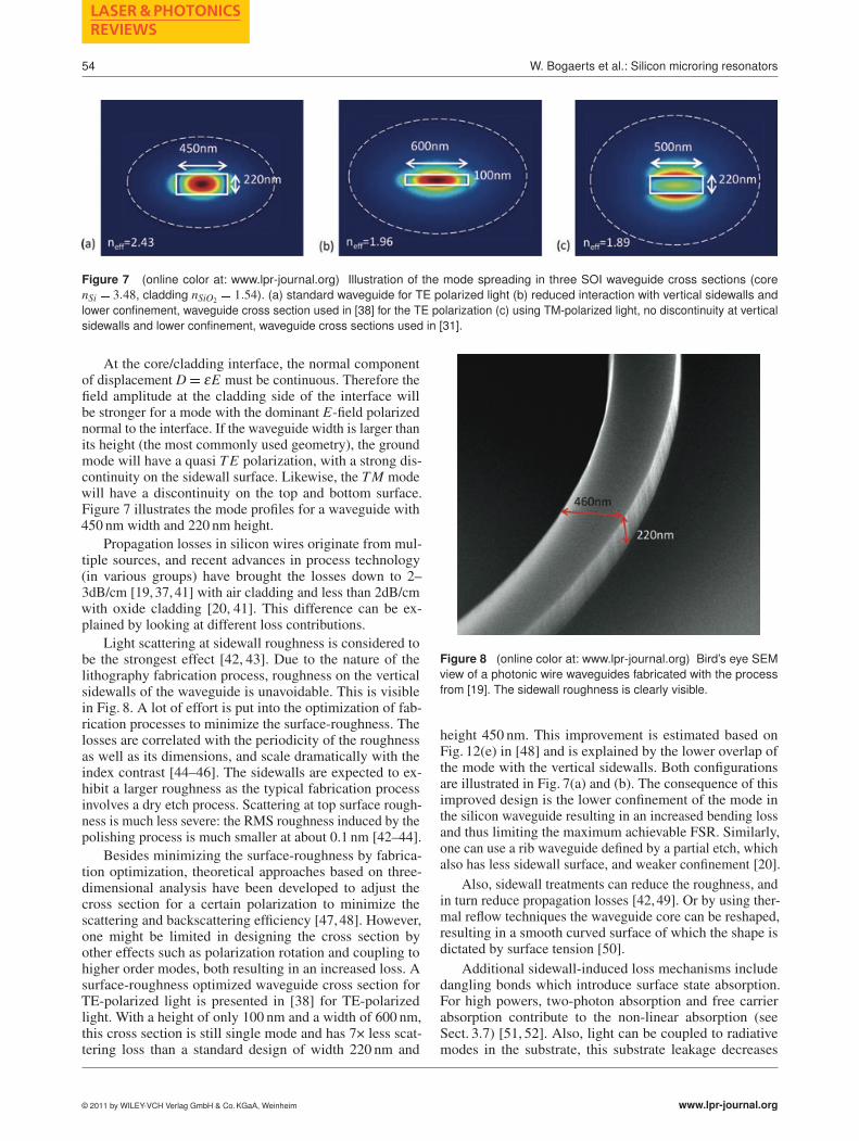
Figure 7 (online color at: www.lpr-journal.org) Illustration of the mode spreading in three SOI waveguide cross sections (corenSi � 3�48, cladding nSiO2
� 1�54). (a) standard waveguide for TE polarized light (b) reduced interaction with vertical sidewalls andlower confinement, waveguide cross section used in [38] for the TE polarization (c) using TM-polarized light, no discontinuity at verticalsidewalls and lower confinement, waveguide cross sections used in [31].
At the core/cladding interface, the normal componentof displacement D� εE must be continuous. Therefore thefield amplitude at the cladding side of the interface willbe stronger for a mode with the dominant E-field polarizednormal to the interface. If the waveguide width is larger thanits height (the most commonly used geometry), the groundmode will have a quasi T E polarization, with a strong dis-continuity on the sidewall surface. Likewise, the T M modewill have a discontinuity on the top and bottom surface.Figure 7 illustrates the mode profiles for a waveguide with450 nm width and 220 nm height.
Propagation losses in silicon wires originate from mul-tiple sources, and recent advances in process technology(in various groups) have brought the losses down to 2–3dB/cm [19, 37, 41] with air cladding and less than 2dB/cmwith oxide cladding [20, 41]. This difference can be ex-plained by looking at different loss contributions.
Light scattering at sidewall roughness is considered tobe the strongest effect [42, 43]. Due to the nature of thelithography fabrication process, roughness on the verticalsidewalls of the waveguide is unavoidable. This is visiblein Fig. 8. A lot of effort is put into the optimization of fab-rication processes to minimize the surface-roughness. Thelosses are correlated with the periodicity of the roughnessas well as its dimensions, and scale dramatically with theindex contrast [44–46]. The sidewalls are expected to ex-hibit a larger roughness as the typical fabrication processinvolves a dry etch process. Scattering at top surface rough-ness is much less severe: the RMS roughness induced by thepolishing process is much smaller at about 0.1 nm [42–44].
Besides minimizing the surface-roughness by fabrica-tion optimization, theoretical approaches based on three-dimensional analysis have been developed to adjust thecross section for a certain polarization to minimize thescattering and backscattering efficiency [47,48]. However,one might be limited in designing the cross section byother effects such as polarization rotation and coupling tohigher order modes, both resulting in an increased loss. Asurface-roughness optimized waveguide cross section forTE-polarized light is presented in [38] for TE-polarizedlight. With a height of only 100 nm and a width of 600 nm,this cross section is still single mode and has 7× less scat-tering loss than a standard design of width 220 nm and
Figure 8 (online color at: www.lpr-journal.org) Bird’s eye SEMview of a photonic wire waveguides fabricated with the processfrom [19]. The sidewall roughness is clearly visible.
height 450 nm. This improvement is estimated based onFig. 12(e) in [48] and is explained by the lower overlap ofthe mode with the vertical sidewalls. Both configurationsare illustrated in Fig. 7(a) and (b). The consequence of thisimproved design is the lower confinement of the mode inthe silicon waveguide resulting in an increased bending lossand thus limiting the maximum achievable FSR. Similarly,one can use a rib waveguide defined by a partial etch, whichalso has less sidewall surface, and weaker confinement [20].
Also, sidewall treatments can reduce the roughness, andin turn reduce propagation losses [42, 49]. Or by using ther-mal reflow techniques the waveguide core can be reshaped,resulting in a smooth curved surface of which the shape isdictated by surface tension [50].
Additional sidewall-induced loss mechanisms includedangling bonds which introduce surface state absorption.For high powers, two-photon absorption and free carrierabsorption contribute to the non-linear absorption (seeSect. 3.7) [51, 52]. Also, light can be coupled to radiativemodes in the substrate, this substrate leakage decreases
© 2011 by WILEY-VCH Verlag GmbH & Co. KGaA, Weinheim www.lpr-journal.org
Laser Photonics Rev. 6, No. 1 (2012)
REVIEWARTICLE
55
exponentially with bottom cladding thickness [53]. For abottom oxide of 2 μm, these losses are negligible for the TEground mode and in the order of 0.001 dB/cm for the TMground mode [43]. The fundamental lower limit of propaga-tion losses is associated to Rayleigh scattering, caused bydeep sub-wavelength index perturbations in the bulk of thewaveguides. When using high-quality crystalline SOI mate-rial, Rayleigh scattering inside the waveguide core materialis expected to be extremely low.
The strong modal confinement (for TE-polarization) inSOI wires allows for very sharp bends (radius down to 3 μm)with still low radiation as compared to bends in conventionalwaveguides (radius down to 100 μm). However, both thesubstrate leakage and scattering loss might be influenced bywaveguide bending, as the mode is pushed outwards (morewith sharper bends). Excess bending losses of a 500 nmwide SOI waveguide amount to 0.01 dB/90� for a 4.5 μmbend, to 0.071 dB/90� for a 1 μm radius bend [19]. Thisexcess bending loss of a circular 90� bend includes modemismatch at the straight-bend interface, coupling betweenTE and TM modes, as well as higher order modes in thebend section and propagation loss in the bends. As bends arean essential component of a ring resonator, the excess bendloss should be kept under control. This can be accomplishedby tuning the waveguide cross section [54] or by engineeringthe bend shape [20].
The patterning process itself can also introduce un-wanted effects depending on the density of the structures.During lithography, (optical) proximity effects can intro-duce linewidth changes which depend on neighboring struc-tures, and during etch, the etch rate can vary based on localdensity (so-called loading effects). This is especially rele-vant in the coupling section, where proximity effects canresult in a rather abrupt change in line width when thewaveguides come close together [19]. Also, the loadingwill impact the line width but also the uniformity of thering resonators [42, 55].
While in general TE-light is the preferred polarization,as TE is the ground mode of the waveguide, there are ad-vantages to using the TM mode: Because of its lower over-lap with the sidewalls, it will experience less scattering,but more essentially, less backscattering. It has been suc-cessfully demonstrated to achieve high-Q microdisk res-onators [28] (whispering-gallery modes) and microring res-onators [31]. Using TM-polarized light in a waveguide crosssection of 500nm�220nm, as shown in Fig. 7(c), more thanan order of magnitude less scattering loss is expected, basedon [48]. This is a result of two effects: First, the electricalfield of the TM mode is oriented mainly in the vertical direc-tion, so no discontinuity is created on the vertical sidewalls.Secondly, the TM mode is less confined in the vertical direc-tion (neff � 1�89), which results in a smaller modal overlapwith the vertical sidewalls. Theoretical predictions by [48]have been verified by backscattering measurements in [29].
Because of the high index contrast, silicon wires arehighly dispersive. This means that the effective index of thepropagating mode is wavelength dependent, so monochro-matic waves of different wavelengths will travel through thewaveguide with different velocities. This causes propagat-
ing pulses (that comprise a sum of monochromatic waves)to broaden and to be delayed (more than due to ordinarywaveguide dispersion). An SOI photonic wire has a normalfirst-order dispersion in the wavelength range of interest andfor the dimensions we performed the characterization on:dneffdλ � 0 [43,56,57]. At ng � 4�3, the group index is almosttwice as large as the effective index. This has a large impacton the spectral characteristics of a ring resonator.
Also, because of the high index contrast and small coresize, photonic wires are exceptionally sensitive to dimen-sional variations. In [42,43] the effect of width and thicknesschanges on the effective index is analyzed. As discussedabove, this is relevant to ring resonators as the effectiveindex determines the optical roundtrip length.
3.2. Directional couplers
The most common way of coupling light from a waveguideto a ring resonator is through a directional coupler. In adirectional coupler, two waveguides are brought close to-gether: This can be done either in a horizontal (side-by-side)arrangement [58,59] or in a vertical arrangement [60]. Al-ternatively, multi-mode interferometers can be used [61].
As we discussed, the coupling between the bus wave-guide and the ring needs to be well controlled to design ringresonators with the desired spectral features. Therefore, agood understanding of the coupling section is crucial. Es-pecially for multistage ring resonators (see Sect. 3.4), thedesign of reproducible directional couplers is one of themain bottlenecks to achieve accurate operation. As siliconphotonic wires are very sensitive to variations, we expectsimilar effects in directional couplers.
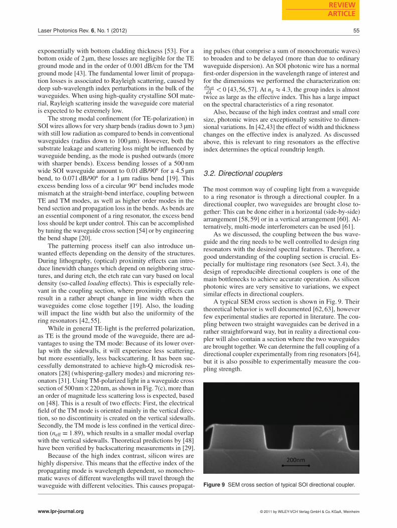
A typical SEM cross section is shown in Fig. 9. Theirtheoretical behavior is well documented [62,63], howeverfew experimental studies are reported in literature. The cou-pling between two straight waveguides can be derived in arather straightforward way, but in reality a directional cou-pler will also contain a section where the two waveguidesare brought together. We can determine the full coupling of adirectional coupler experimentally from ring resonators [64],but it is also possible to experimentally measure the cou-pling strength.
Figure 9 SEM cross section of typical SOI directional coupler.
www.lpr-journal.org © 2011 by WILEY-VCH Verlag GmbH & Co. KGaA, Weinheim
56
LASER & PHOTONICSREVIEWS
W. Bogaerts et al.: Silicon microring resonators
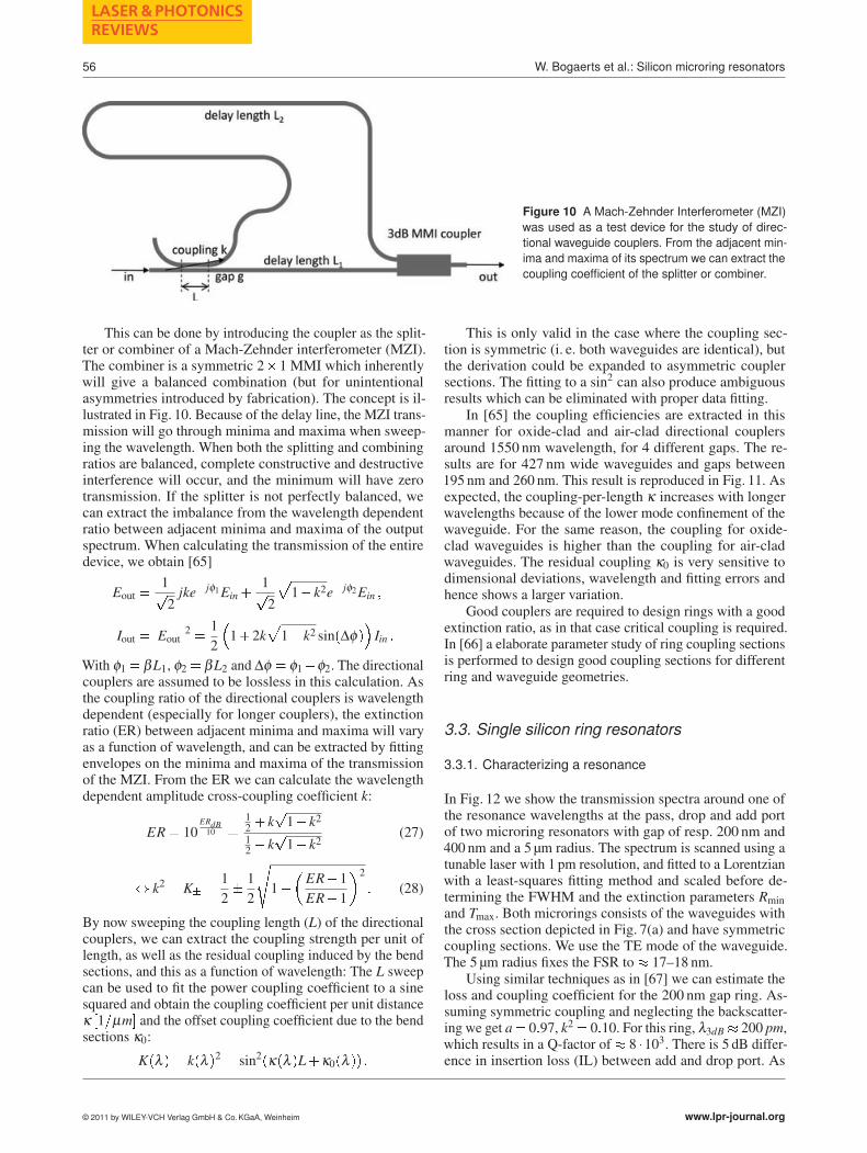
Figure 10 A Mach-Zehnder Interferometer (MZI)was used as a test device for the study of direc-tional waveguide couplers. From the adjacent min-ima and maxima of its spectrum we can extract thecoupling coefficient of the splitter or combiner.
This can be done by introducing the coupler as the split-ter or combiner of a Mach-Zehnder interferometer (MZI).The combiner is a symmetric 2�1 MMI which inherentlywill give a balanced combination (but for unintentionalasymmetries introduced by fabrication). The concept is il-lustrated in Fig. 10. Because of the delay line, the MZI trans-mission will go through minima and maxima when sweep-ing the wavelength. When both the splitting and combiningratios are balanced, complete constructive and destructiveinterference will occur, and the minimum will have zerotransmission. If the splitter is not perfectly balanced, wecan extract the imbalance from the wavelength dependentratio between adjacent minima and maxima of the outputspectrum. When calculating the transmission of the entiredevice, we obtain [65]
Eout �1�2
jke� jφ1Ein �1�2
�1� k2e� jφ2Ein �
Iout � �Eout�2 � 1
2
�1�2k
�1� k2 sin�Δφ�
�Iin �
With φ1 � βL1, φ2 � βL2 and Δφ � φ1�φ2. The directionalcouplers are assumed to be lossless in this calculation. Asthe coupling ratio of the directional couplers is wavelengthdependent (especially for longer couplers), the extinctionratio (ER) between adjacent minima and maxima will varyas a function of wavelength, and can be extracted by fittingenvelopes on the minima and maxima of the transmissionof the MZI. From the ER we can calculate the wavelengthdependent amplitude cross-coupling coefficient k:
ER � 10ERdB10 �
12 � k
�1� k2
12 � k
�1� k2
(27)
� k2 � K� �1
2� 1
2
�1�
�ER�1
ER�1
�2
� (28)
By now sweeping the coupling length (L) of the directionalcouplers, we can extract the coupling strength per unit oflength, as well as the residual coupling induced by the bendsections, and this as a function of wavelength: The L sweepcan be used to fit the power coupling coefficient to a sinesquared and obtain the coupling coefficient per unit distanceκ �1�μm� and the offset coupling coefficient due to the bendsections κ0:
K�λ � � k�λ �2 � sin2�κ�λ �L�κ0�λ �� �
This is only valid in the case where the coupling sec-tion is symmetric (i. e. both waveguides are identical), butthe derivation could be expanded to asymmetric couplersections. The fitting to a sin2 can also produce ambiguousresults which can be eliminated with proper data fitting.
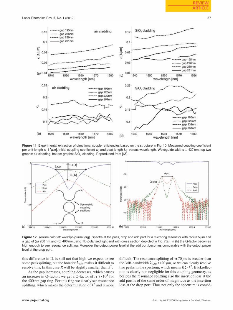
In [65] the coupling efficiencies are extracted in thismanner for oxide-clad and air-clad directional couplersaround 1550 nm wavelength, for 4 different gaps. The re-sults are for 427 nm wide waveguides and gaps between195 nm and 260 nm. This result is reproduced in Fig. 11. Asexpected, the coupling-per-length κ increases with longerwavelengths because of the lower mode confinement of thewaveguide. For the same reason, the coupling for oxide-clad waveguides is higher than the coupling for air-cladwaveguides. The residual coupling κ0 is very sensitive todimensional deviations, wavelength and fitting errors andhence shows a larger variation.
Good couplers are required to design rings with a goodextinction ratio, as in that case critical coupling is required.In [66] a elaborate parameter study of ring coupling sectionsis performed to design good coupling sections for differentring and waveguide geometries.
3.3. Single silicon ring resonators
3.3.1. Characterizing a resonance
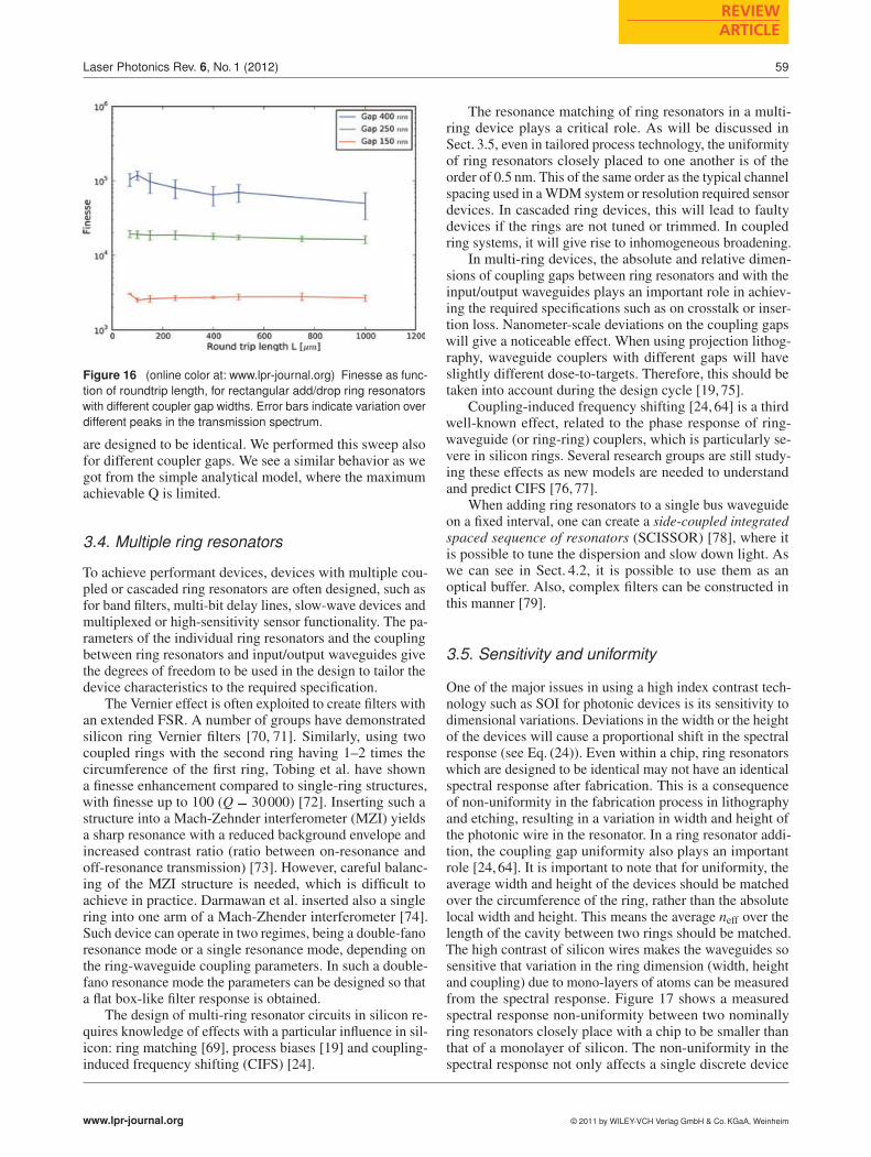
In Fig. 12 we show the transmission spectra around one ofthe resonance wavelengths at the pass, drop and add portof two microring resonators with gap of resp. 200 nm and400 nm and a 5 μm radius. The spectrum is scanned using atunable laser with 1 pm resolution, and fitted to a Lorentzianwith a least-squares fitting method and scaled before de-termining the FWHM and the extinction parameters Rmin
and Tmax. Both microrings consists of the waveguides withthe cross section depicted in Fig. 7(a) and have symmetriccoupling sections. We use the TE mode of the waveguide.The 5 μm radius fixes the FSR to � 17–18 nm.
Using similar techniques as in [67] we can estimate theloss and coupling coefficient for the 200 nm gap ring. As-suming symmetric coupling and neglecting the backscatter-ing we get a� 0�97, k2 � 0�10. For this ring, λ3dB � 200 pm,which results in a Q-factor of � 8 �103. There is 5 dB differ-ence in insertion loss (IL) between add and drop port. As
© 2011 by WILEY-VCH Verlag GmbH & Co. KGaA, Weinheim www.lpr-journal.org
Laser Photonics Rev. 6, No. 1 (2012)
REVIEWARTICLE
57
Figure 11 Experimental extraction of directional coupler efficiencies based on the structure in Fig. 10. Measured coupling coefficientper unit length κ �1�μm�, initial coupling coefficient κ0 and beat length L π
2versus wavelength. Waveguide widths � 427nm, top two
graphs: air cladding, bottom graphs: SiO2 cladding. Reproduced from [65].
Figure 12 (online color at: www.lpr-journal.org) Spectra at the pass, drop and add port for a microring resonator with radius 5 μm anda gap of (a) 200 nm and (b) 400 nm using TE-polarized light and with cross section depicted in Fig. 7(a). In (b) the Q-factor becomeshigh enough to see resonance splitting. Moreover the output power level at the add port becomes comparable with the output powerlevel at the drop port.
this difference in IL is still not that high we expect to seesome peaksplitting, but the broader λ3dB makes it difficult toresolve this. In this case R will be slightly smaller than k2.
As the gap increases, coupling decreases, which causesan increase in Q-factor: we get a Q-factor of � 8 �104 forthe 400 nm gap ring. For this ring we clearly see resonancesplitting, which makes the determination of k2 and a more
difficult. The resonance splitting of � 70 pm is broader thanthe 3dB-bandwidth λ3dB � 20 pm, so we can clearly resolvetwo peaks in the spectrum, which means R� k2. Backreflec-tion is clearly non negligible for this coupling geometry, asbesides the resonance splitting also the insertion loss at theadd port is of the same order of magnitude as the insertionloss at the drop port. Thus not only the spectrum is consid-
www.lpr-journal.org © 2011 by WILEY-VCH Verlag GmbH & Co. KGaA, Weinheim

58
LASER & PHOTONICSREVIEWS
W. Bogaerts et al.: Silicon microring resonators
erably disturbed, but also the direction of the power flow inthe microring is heavily modified. Similar remarks hold forthe other resonance peaks in the spectra of both rings. Thesetwo examples clearly illustrate backscattering is a majorissue when trying to design circuits based on high Q-rings.
3.3.2. FSR and group index
The group index can be determined experimentally by mea-suring the FSR of ring resonators with various round triplengths: the test device is a rounded rectangular resonator(bend radius 4.5 μm), with a variation of the vertical straightsection, while the coupling sections of 2 μm remain unaf-fected. Figure 13 shows the FSR as a function of the roundtrip length of a racetrack add-drop resonator. The waveguidedimensions are 450nm�220nm. The group index ng is de-termined by fitting formula (9) to the measured values of theFSR (measured ng � 4�30). In Fig. 14 we see the change inQ factor with the length of the ring, as we expect from (22).
Figure 13 (online color at: www.lpr-journal.org) FSR plotted asfunction of roundtrip length. We see the FSR� 1
L behavior fromformula (9) corresponding to an ng of 4.30.
Figure 14 (online color at: www.lpr-journal.org) Q as function ofwavelength for different ring lengths, with a coupler gap of 150 nm.
3.3.3. Losses and coupling
On the same set of devices we perform the analysis fromSect. 2.4, for different values of the gap width in the cou-pling section (g � 150 nm, 250 nm, 400 nm). We did notexamine asymmetrical ring resonators because the error onmeasurements and fitting was too large to solve the sys-tem with three equations for a, r1, and r2. Therefore, wesimplified the situation by using a symmetrical add-dropresonator. However, even then it is not straightforward todiscriminate between the losses introduced by the couplingsections and those introduced by the ring itself. In an APF,a and r are even completely interchangeable, so it is not pos-sible to distinguish them from the spectral characteristics. Afirst method to circumvent this issue was published by Mc-Kinnon et al. in [68]. They measure the transmission overa broad wavelength range and disentangle a and r basedon how these parameters vary with wavelength. A secondapproach to solve this problem is, besides to determine thespectral intensity dependence of the microring, to measurethe induced phaseshift of the resonator by inserting it in onearm of a nearly balanced MZI [16]. In an analoguous way,using the combined information from the measurement ofan add-drop filter and a complementary APF (i. e. with thesame coupling gap), it is even possible to make a distinc-tion between the loss in the coupling section and the loss inthe ring waveguides [67]. A drawback of the approach tocalculate ring parameters using the combined informationfrom measurement of different, although complementary,structures is that chip-uniformity problems can disturb theresults [69]. A third manner to disentangle r and a is tomeasure parameter sweeps of rings which differ only inone parameter (in this case the length of the straight sec-tion, or the gap width in the coupling section). Figures 15and 16 plot the Q and finesse as a function of roundtriplength, for rectangular rings where only the roundtrip lengthis varied by changing the straight section that is not coupledto a waveguide. The bend radius and directional couplers
Figure 15 (online color at: www.lpr-journal.org) Q as functionof roundtrip length, for rectangular add/drop ring resonators withdifferent coupler gap widths. Error bars indicate variation overdifferent peaks in the transmission spectrum.
© 2011 by WILEY-VCH Verlag GmbH & Co. KGaA, Weinheim www.lpr-journal.org
Laser Photonics Rev. 6, No. 1 (2012)
REVIEWARTICLE
59
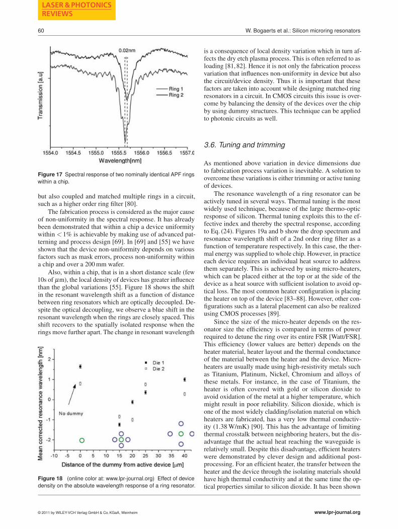
Figure 16 (online color at: www.lpr-journal.org) Finesse as func-tion of roundtrip length, for rectangular add/drop ring resonatorswith different coupler gap widths. Error bars indicate variation overdifferent peaks in the transmission spectrum.
are designed to be identical. We performed this sweep alsofor different coupler gaps. We see a similar behavior as wegot from the simple analytical model, where the maximumachievable Q is limited.
3.4. Multiple ring resonators
To achieve performant devices, devices with multiple cou-pled or cascaded ring resonators are often designed, such asfor band filters, multi-bit delay lines, slow-wave devices andmultiplexed or high-sensitivity sensor functionality. The pa-rameters of the individual ring resonators and the couplingbetween ring resonators and input/output waveguides givethe degrees of freedom to be used in the design to tailor thedevice characteristics to the required specification.
The Vernier effect is often exploited to create filters withan extended FSR. A number of groups have demonstratedsilicon ring Vernier filters [70, 71]. Similarly, using twocoupled rings with the second ring having 1–2 times thecircumference of the first ring, Tobing et al. have showna finesse enhancement compared to single-ring structures,with finesse up to 100 (Q � 30000) [72]. Inserting such astructure into a Mach-Zehnder interferometer (MZI) yieldsa sharp resonance with a reduced background envelope andincreased contrast ratio (ratio between on-resonance andoff-resonance transmission) [73]. However, careful balanc-ing of the MZI structure is needed, which is difficult toachieve in practice. Darmawan et al. inserted also a singlering into one arm of a Mach-Zhender interferometer [74].Such device can operate in two regimes, being a double-fanoresonance mode or a single resonance mode, depending onthe ring-waveguide coupling parameters. In such a double-fano resonance mode the parameters can be designed so thata flat box-like filter response is obtained.
The design of multi-ring resonator circuits in silicon re-quires knowledge of effects with a particular influence in sil-icon: ring matching [69], process biases [19] and coupling-induced frequency shifting (CIFS) [24].
The resonance matching of ring resonators in a multi-ring device plays a critical role. As will be discussed inSect. 3.5, even in tailored process technology, the uniformityof ring resonators closely placed to one another is of theorder of 0.5 nm. This of the same order as the typical channelspacing used in aWDM system or resolution required sensordevices. In cascaded ring devices, this will lead to faultydevices if the rings are not tuned or trimmed. In coupledring systems, it will give rise to inhomogeneous broadening.
In multi-ring devices, the absolute and relative dimen-sions of coupling gaps between ring resonators and with theinput/output waveguides plays an important role in achiev-ing the required specifications such as on crosstalk or inser-tion loss. Nanometer-scale deviations on the coupling gapswill give a noticeable effect. When using projection lithog-raphy, waveguide couplers with different gaps will haveslightly different dose-to-targets. Therefore, this should betaken into account during the design cycle [19, 75].
Coupling-induced frequency shifting [24, 64] is a thirdwell-known effect, related to the phase response of ring-waveguide (or ring-ring) couplers, which is particularly se-vere in silicon rings. Several research groups are still study-ing these effects as new models are needed to understandand predict CIFS [76, 77].
When adding ring resonators to a single bus waveguideon a fixed interval, one can create a side-coupled integratedspaced sequence of resonators (SCISSOR) [78], where itis possible to tune the dispersion and slow down light. Aswe can see in Sect. 4.2, it is possible to use them as anoptical buffer. Also, complex filters can be constructed inthis manner [79].
3.5. Sensitivity and uniformity
One of the major issues in using a high index contrast tech-nology such as SOI for photonic devices is its sensitivity todimensional variations. Deviations in the width or the heightof the devices will cause a proportional shift in the spectralresponse (see Eq. (24)). Even within a chip, ring resonatorswhich are designed to be identical may not have an identicalspectral response after fabrication. This is a consequenceof non-uniformity in the fabrication process in lithographyand etching, resulting in a variation in width and height ofthe photonic wire in the resonator. In a ring resonator addi-tion, the coupling gap uniformity also plays an importantrole [24, 64]. It is important to note that for uniformity, theaverage width and height of the devices should be matchedover the circumference of the ring, rather than the absolutelocal width and height. This means the average neff over thelength of the cavity between two rings should be matched.The high contrast of silicon wires makes the waveguides sosensitive that variation in the ring dimension (width, heightand coupling) due to mono-layers of atoms can be measuredfrom the spectral response. Figure 17 shows a measuredspectral response non-uniformity between two nominallyring resonators closely place with a chip to be smaller thanthat of a monolayer of silicon. The non-uniformity in thespectral response not only affects a single discrete device
www.lpr-journal.org © 2011 by WILEY-VCH Verlag GmbH & Co. KGaA, Weinheim
60
LASER & PHOTONICSREVIEWS
W. Bogaerts et al.: Silicon microring resonators
Figure 17 Spectral response of two nominally identical APF ringswithin a chip.
but also coupled and matched multiple rings in a circuit,such as a higher order ring filter [80].
The fabrication process is considered as the major causeof non-uniformity in the spectral response. It has alreadybeen demonstrated that within a chip a device uniformitywithin � 1% is achievable by making use of advanced pat-terning and process design [69]. In [69] and [55] we haveshown that the device non-uniformity depends on variousfactors such as mask errors, process non-uniformity withina chip and over a 200mm wafer.
Also, within a chip, that is in a short distance scale (few10s of μm), the local density of devices has greater influencethan the global variations [55]. Figure 18 shows the shiftin the resonant wavelength shift as a function of distancebetween ring resonators which are optically decoupled. De-spite the optical decoupling, we observe a blue shift in theresonant wavelength when the rings are closely spaced. Thisshift recovers to the spatially isolated response when therings move further apart. The change in resonant wavelength
Figure 18 (online color at: www.lpr-journal.org) Effect of devicedensity on the absolute wavelength response of a ring resonator.
is a consequence of local density variation which in turn af-fects the dry etch plasma process. This is often referred to asloading [81, 82]. Hence it is not only the fabrication processvariation that influences non-uniformity in device but alsothe circuit/device density. Thus it is important that thesefactors are taken into account while designing matched ringresonators in a circuit. In CMOS circuits this issue is over-come by balancing the density of the devices over the chipby using dummy structures. This technique can be appliedto photonic circuits as well.
3.6. Tuning and trimming
As mentioned above variation in device dimensions dueto fabrication process variation is inevitable. A solution toovercome these variations is either trimming or active tuningof devices.
The resonance wavelength of a ring resonator can beactively tuned in several ways. Thermal tuning is the mostwidely used technique, because of the large thermo-opticresponse of silicon. Thermal tuning exploits this to the ef-fective index and thereby the spectral response, accordingto Eq. (24). Figures 19a and b show the drop spectrum andresonance wavelength shift of a 2nd order ring filter as afunction of temperature respectively. In this case, the ther-mal energy was supplied to whole chip. However, in practiceeach device requires an individual heat source to addressthem separately. This is achieved by using micro-heaters,which can be placed either at the top or at the side of thedevice as a heat source with sufficient isolation to avoid op-tical loss. The most common heater configuration is placingthe heater on top of the device [83–88]. However, other con-figurations such as a lateral placement can also be realizedusing CMOS processes [89].
Since the size of the micro-heater depends on the res-onator size the efficiency is compared in terms of powerrequired to detune the ring over its entire FSR [Watt/FSR].This efficiency (lower values are better) depends on theheater material, heater layout and the thermal conductanceof the material between the heater and the device. Micro-heaters are usually made using high-resistivity metals suchas Titanium, Platinum, Nickel, Chromium and alloys ofthese metals. For instance, in the case of Titanium, theheater is often covered with gold or silicon dioxide toavoid oxidation of the metal at a higher temperature, whichmight result in poor reliability. Silicon dioxide, which isone of the most widely cladding/isolation material on whichheaters are fabricated, has a very low thermal conductiv-ity (1.38W/mK) [90]. This has the advantage of limitingthermal crosstalk between neighboring heaters, but the dis-advantage that the actual heat reaching the waveguide isrelatively small. Despite this disadvantage, efficient heaterswere demonstrated by clever design and additional post-processing. For an efficient heater, the transfer between theheater and the device through the isolating materials shouldhave high thermal conductivity and at the same time the op-tical properties similar to silicon dioxide. It has been shown
© 2011 by WILEY-VCH Verlag GmbH & Co. KGaA, Weinheim www.lpr-journal.org
Laser Photonics Rev. 6, No. 1 (2012)
REVIEWARTICLE
61
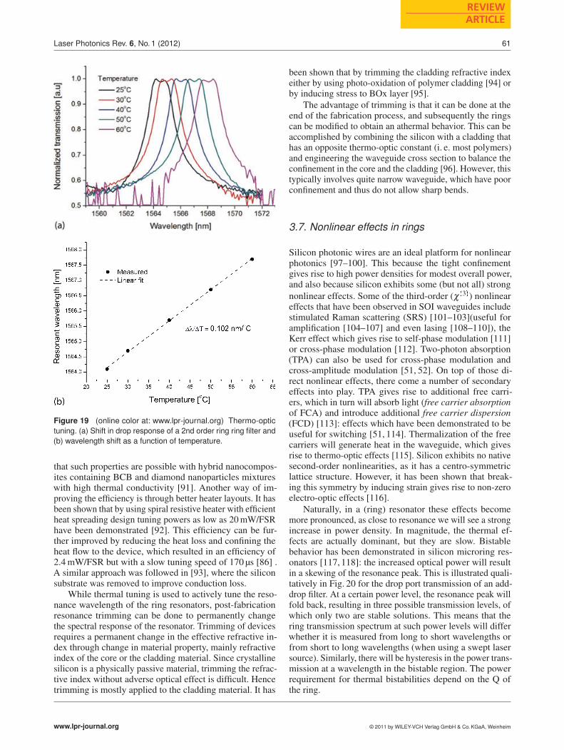
Figure 19 (online color at: www.lpr-journal.org) Thermo-optictuning. (a) Shift in drop response of a 2nd order ring ring filter and(b) wavelength shift as a function of temperature.
that such properties are possible with hybrid nanocompos-ites containing BCB and diamond nanoparticles mixtureswith high thermal conductivity [91]. Another way of im-proving the efficiency is through better heater layouts. It hasbeen shown that by using spiral resistive heater with efficientheat spreading design tuning powers as low as 20mW/FSRhave been demonstrated [92]. This efficiency can be fur-ther improved by reducing the heat loss and confining theheat flow to the device, which resulted in an efficiency of2.4mW/FSR but with a slow tuning speed of 170 μs [86] .A similar approach was followed in [93], where the siliconsubstrate was removed to improve conduction loss.
While thermal tuning is used to actively tune the reso-nance wavelength of the ring resonators, post-fabricationresonance trimming can be done to permanently changethe spectral response of the resonator. Trimming of devicesrequires a permanent change in the effective refractive in-dex through change in material property, mainly refractiveindex of the core or the cladding material. Since crystallinesilicon is a physically passive material, trimming the refrac-tive index without adverse optical effect is difficult. Hencetrimming is mostly applied to the cladding material. It has
been shown that by trimming the cladding refractive indexeither by using photo-oxidation of polymer cladding [94] orby inducing stress to BOx layer [95].
The advantage of trimming is that it can be done at theend of the fabrication process, and subsequently the ringscan be modified to obtain an athermal behavior. This can beaccomplished by combining the silicon with a cladding thathas an opposite thermo-optic constant (i. e. most polymers)and engineering the waveguide cross section to balance theconfinement in the core and the cladding [96]. However, thistypically involves quite narrow waveguide, which have poorconfinement and thus do not allow sharp bends.
3.7. Nonlinear effects in rings
Silicon photonic wires are an ideal platform for nonlinearphotonics [97–100]. This because the tight confinementgives rise to high power densities for modest overall power,and also because silicon exhibits some (but not all) strong
nonlinear effects. Some of the third-order (χ�3�) nonlineareffects that have been observed in SOI waveguides includestimulated Raman scattering (SRS) [101–103](useful foramplification [104–107] and even lasing [108–110]), theKerr effect which gives rise to self-phase modulation [111]or cross-phase modulation [112]. Two-photon absorption(TPA) can also be used for cross-phase modulation andcross-amplitude modulation [51, 52]. On top of those di-rect nonlinear effects, there come a number of secondaryeffects into play. TPA gives rise to additional free carri-ers, which in turn will absorb light (free carrier absorptionof FCA) and introduce additional free carrier dispersion(FCD) [113]: effects which have been demonstrated to beuseful for switching [51, 114]. Thermalization of the freecarriers will generate heat in the waveguide, which givesrise to thermo-optic effects [115]. Silicon exhibits no nativesecond-order nonlinearities, as it has a centro-symmetriclattice structure. However, it has been shown that break-ing this symmetry by inducing strain gives rise to non-zeroelectro-optic effects [116].
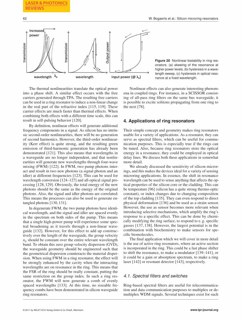
Naturally, in a (ring) resonator these effects becomemore pronounced, as close to resonance we will see a strongincrease in power density. In magnitude, the thermal ef-fects are actually dominant, but they are slow. Bistablebehavior has been demonstrated in silicon microring res-onators [117, 118]: the increased optical power will resultin a skewing of the resonance peak. This is illustrated quali-tatively in Fig. 20 for the drop port transmission of an add-drop filter. At a certain power level, the resonance peak willfold back, resulting in three possible transmission levels, ofwhich only two are stable solutions. This means that thering transmission spectrum at such power levels will differwhether it is measured from long to short wavelengths orfrom short to long wavelengths (when using a swept lasersource). Similarly, there will be hysteresis in the power trans-mission at a wavelength in the bistable region. The powerrequirement for thermal bistabilities depend on the Q ofthe ring.
www.lpr-journal.org © 2011 by WILEY-VCH Verlag GmbH & Co. KGaA, Weinheim
62
LASER & PHOTONICSREVIEWS
W. Bogaerts et al.: Silicon microring resonators
Figure 20 Nonlinear bistability in ring res-onators. (a) skewing of the resonance athigher power levels, (b) hysteresis in a wave-length sweep, (c) hysteresis in optical reso-nance at a fixed wavelength.
The thermal nonlinearities translate the optical powerinto a phase shift. A similar effect occurs with the freecarriers generated through TPA. The resulting free carrierscan be used in a ring resonator to induce a non-linear changein the real part of the refractive index [115, 119]. Thesecarrier effects are much faster than thermal effects. Whencombining both effects with a different time scale, this canresult in self-pulsing behavior [120].
By definition, nonlinear effects will generate additionalfrequency components in a signal. As silicon has no intrin-sic second-order nonlinearities, there will be no generationof second harmonics. However, the third-order nonlinear-ity (Kerr effect) is quite strong, and the resulting greenemission of third-harmonic generation has already beendemonstrated [121]. This also means that wavelengths ina waveguide are no longer independent, and that nonlin-earities will generate new wavelengths through four-wavemixing (FWM) [122]. In FWM, two pump photons inter-act and result in two new photons (a signal photon and anidler) at different frequencies [123]. This can be used forwavelength conversion [124–127] and all-optical signal pro-cessing [128, 129]. Obviously, the total energy of the newphotons should be the same as the energy of the originalphotons. Also, the signal and idler photons are correlated:This means the processes can also be used to generate en-tangled photons [130,131].
In degenerate FWM, the two pump photons have identi-cal wavelength, and the signal and idler are spaced evenlyin the spectrum on both sides of the pump. This meansthat a single high-power pump will experience some spec-tral broadening as it travels through a non-linear wave-guide [132]. However, for this effect to add up construc-tively over the length of the waveguide, the group velocityng should be constant over the entire relevant wavelengthband. To obtain this zero group velocity dispersion (GVD),the waveguide geometry should be engineered such thatthe geometrical dispersion counteracts the material disper-sion. When using FWM in a ring resonator, the effect willbe strongly enhanced by the cavity when the interactingwavelengths are on resonance in the ring. This means thatthe FSR of the ring should be really constant, putting thesame restriction on the group index. In such a ring res-onator, the FWM will now generate a comb of evenlyspaced wavelengths [133]. At this time, no sizeable fre-quency combs have been demonstrated in silicon waveguidering resonators.
Nonlinear effects can also generate interesting phenom-ena in coupled rings. For instance, in a SCISSOR consist-ing of all-pass ring filters on the same bus waveguide, itis possible to excite solitons propagating from one ring tothe next [78].
4. Applications of ring resonators
Their simple concept and geometry makes ring resonatorsusable for a variety of applications. As a resonator, they canserve as spectral filters, which can be useful for commu-nication purposes. This is especially true if the rings canbe tuned. Also, because ring resonators store the opticalenergy in a resonance, they could be employed in opticaldelay lines. We discuss both these applications in somewhatmore detail.
We already discussed the sensitivity of silicon micror-ings, and this makes the devices ideal for a variety of sensingmicroring applications. In essence, the shift in resonancewavelength can be used to sense anything that affects the op-tical properties of the silicon core or the cladding. This canbe temperature [96] (silicon has a quite strong thermo-opticconstant), or index changes due to changing compositionof the top cladding [135]. They can even respond to directphysical deformation [136] and be used as a strain sensor.However, the use as sensor becomes more relevant whenintroducing selective mechanisms, which amplify the ring’sresponse to a specific effect. This can be done by chemi-cally modifying the ring surface, to respond to e. g. specificgasses [137, 138]. However, the largest potential is in thecombination with biochemistry to make sensors for spe-cific biomolecules.
The final application which we will cover in more detailis the use of active ring resonators, where an active sectionis incorporated in the ring. This could be a fast phase shifterto shift the resonance, to make a modulator [139–141], orit could be a gain or absorption spectrum, to make a ringlaser [142] or resonant detector [143], respectively.
4.1. Spectral filters and switches
Ring-based spectral filters are useful for telecommunica-tion and data communication purposes to multiplex or de-multiplex WDM signals. Several techniques exist for such
© 2011 by WILEY-VCH Verlag GmbH & Co. KGaA, Weinheim www.lpr-journal.org
Laser Photonics Rev. 6, No. 1 (2012)
REVIEWARTICLE
63
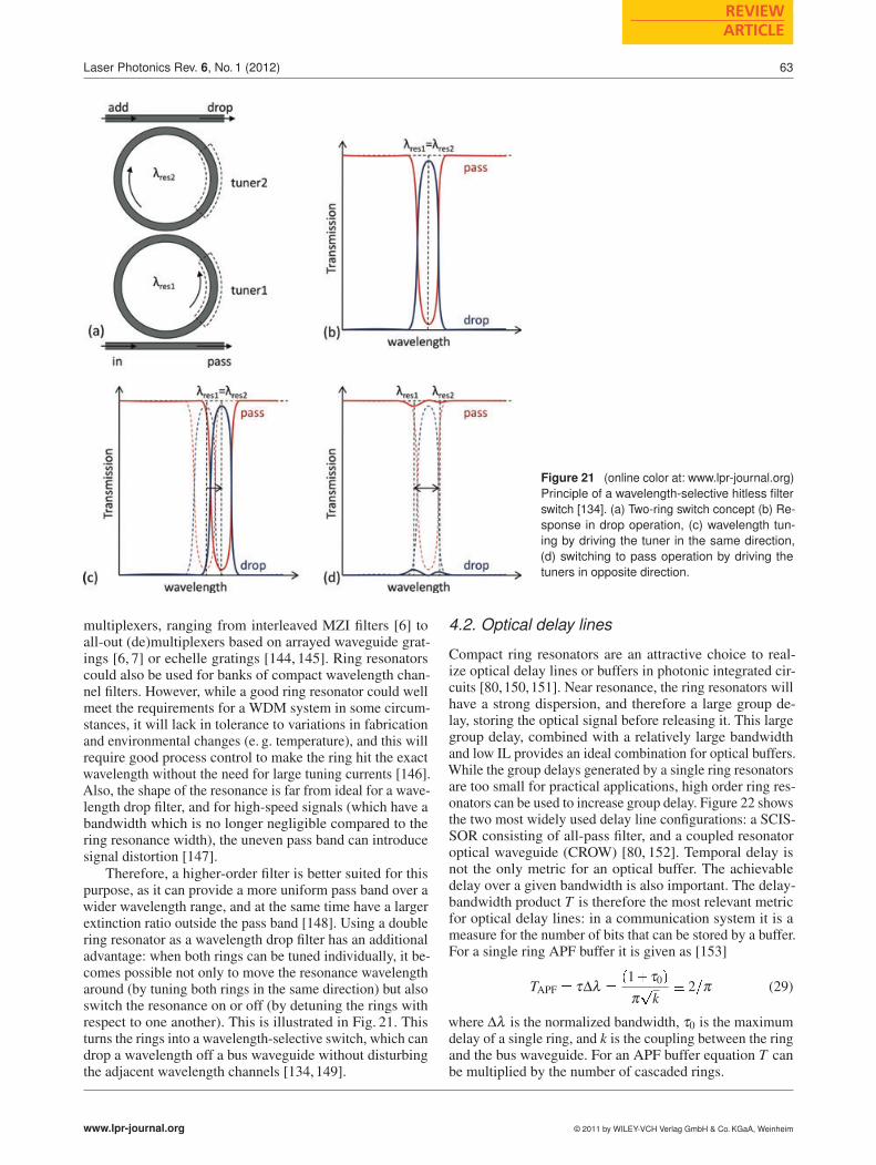
Figure 21 (online color at: www.lpr-journal.org)Principle of a wavelength-selective hitless filterswitch [134]. (a) Two-ring switch concept (b) Re-sponse in drop operation, (c) wavelength tun-ing by driving the tuner in the same direction,(d) switching to pass operation by driving thetuners in opposite direction.
multiplexers, ranging from interleaved MZI filters [6] toall-out (de)multiplexers based on arrayed waveguide grat-ings [6, 7] or echelle gratings [144, 145]. Ring resonatorscould also be used for banks of compact wavelength chan-nel filters. However, while a good ring resonator could wellmeet the requirements for a WDM system in some circum-stances, it will lack in tolerance to variations in fabricationand environmental changes (e. g. temperature), and this willrequire good process control to make the ring hit the exactwavelength without the need for large tuning currents [146].Also, the shape of the resonance is far from ideal for a wave-length drop filter, and for high-speed signals (which have abandwidth which is no longer negligible compared to thering resonance width), the uneven pass band can introducesignal distortion [147].
Therefore, a higher-order filter is better suited for thispurpose, as it can provide a more uniform pass band over awider wavelength range, and at the same time have a largerextinction ratio outside the pass band [148]. Using a doublering resonator as a wavelength drop filter has an additionaladvantage: when both rings can be tuned individually, it be-comes possible not only to move the resonance wavelengtharound (by tuning both rings in the same direction) but alsoswitch the resonance on or off (by detuning the rings withrespect to one another). This is illustrated in Fig. 21. Thisturns the rings into a wavelength-selective switch, which candrop a wavelength off a bus waveguide without disturbingthe adjacent wavelength channels [134, 149].
4.2. Optical delay lines
Compact ring resonators are an attractive choice to real-ize optical delay lines or buffers in photonic integrated cir-cuits [80,150,151]. Near resonance, the ring resonators willhave a strong dispersion, and therefore a large group de-lay, storing the optical signal before releasing it. This largegroup delay, combined with a relatively large bandwidthand low IL provides an ideal combination for optical buffers.While the group delays generated by a single ring resonatorsare too small for practical applications, high order ring res-onators can be used to increase group delay. Figure 22 showsthe two most widely used delay line configurations: a SCIS-SOR consisting of all-pass filter, and a coupled resonatoroptical waveguide (CROW) [80, 152]. Temporal delay isnot the only metric for an optical buffer. The achievabledelay over a given bandwidth is also important. The delay-bandwidth product T is therefore the most relevant metricfor optical delay lines: in a communication system it is ameasure for the number of bits that can be stored by a buffer.For a single ring APF buffer it is given as [153]
TAPF � τΔλ ��1� τ0�
π�
k� 2�π (29)
where Δλ is the normalized bandwidth, τ0 is the maximumdelay of a single ring, and k is the coupling between the ringand the bus waveguide. For an APF buffer equation T canbe multiplied by the number of cascaded rings.
www.lpr-journal.org © 2011 by WILEY-VCH Verlag GmbH & Co. KGaA, Weinheim
64
LASER & PHOTONICSREVIEWS
W. Bogaerts et al.: Silicon microring resonators
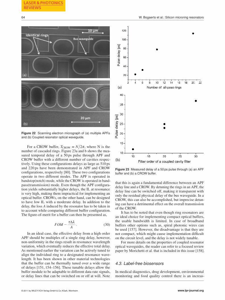
Figure 22 Scanning electron micrograph of (a) multiple APFsand (b) Coupled resonator optical waveguide.
For a CROW buffer, TCROW � N�2π , where N is thenumber of cascaded rings. Figure 23a and b shows the mea-sured temporal delay of a 50 ps pulse through APF andCROW buffer with a different number of cavities respec-tively. Using these configurations delays as large as 510 psand 220 ps have been demonstrated in APF and CROWconfigurations, respectively [80]. These two configurationsoperate in two different modes. The APF is operated inbandstop(notch) mode, while the CROW is operated in band-pass(transmission) mode. Even though the APF configura-tion yields substantially higher delays, the IL at resonanceis very high, making them impractical for implementing anoptical buffer. CROWs, on the other hand, can be designedto have low IL with a moderate delay. In addition to thedelay, the loss A induced by the resonator has to be taken into account while comparing different buffer configuration.The figure-of-merit for a buffer can then be presented as,
FOM �
τΔλA
� (30)
In an ideal case, the effective delay from a high orderAPF should be multiples of a single ring delay, however,non-uniformity in the rings result in resonance wavelengthvariation, which eventually reduces the effective total delay.As mentioned earlier the variation can be actively tuned toalign the individual ring to a designated resonance wave-length. It has been shown in other material technologiesthat the buffer can be thermally tuned over a wide rangeof delays [151, 154–156]. These tunable delays allow thebuffer module to be adaptable to different data rate signals,or delay lines that can be switched on or off at will. Note
Figure 23 Measured delay of a 50 ps pulse through (a) an APFbuffer and (b) a CROW buffer.
that this is again a fundamental difference between an APFdelay line and a CROW. By detuning the rings in an APF, thedelay line can be switched off, making it transparent withonly the residual physical delay of the bus waveguide. In aCROW, this can also be accomplished, but imprecise detun-ing can have a detrimental effect on the overall transmissionof the CROW.
It has to be noted that even though ring resonators arean ideal choice for implementing compact optical buffers,the usable bandwidth is limited. In case of broadbandbuffers other options such as, spiral photonic wires canbe used [157]. However, the disadvantage is that they arenot compact, which might cause implementation difficulton the circuit level, and the delay is not widely tunable.
For more details on the properties of coupled resonatoroptical waveguides, the reader can refer to a focused reviewpaper by Morichetti et al. that is included in this issue [158].
4.3. Label-free biosensors
In medical diagnostics, drug development, environmentalmonitoring and food quality control there is an increas-
© 2011 by WILEY-VCH Verlag GmbH & Co. KGaA, Weinheim www.lpr-journal.org
Laser Photonics Rev. 6, No. 1 (2012)
REVIEWARTICLE
65
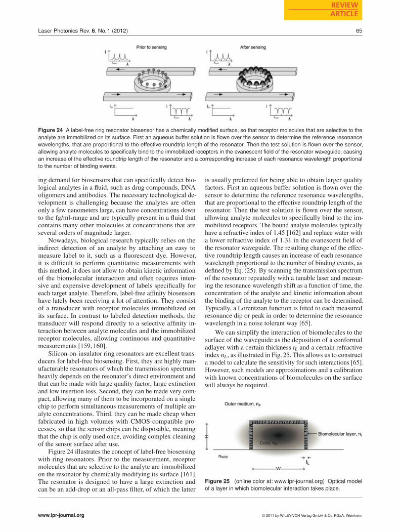
Figure 24 A label-free ring resonator biosensor has a chemically modified surface, so that receptor molecules that are selective to theanalyte are immobilized on its surface. First an aqueous buffer solution is flown over the sensor to determine the reference resonancewavelengths, that are proportional to the effective roundtrip length of the resonator. Then the test solution is flown over the sensor,allowing analyte molecules to specifically bind to the immobilized receptors in the evanescent field of the resonator waveguide, causingan increase of the effective roundtrip length of the resonator and a corresponding increase of each resonance wavelength proportionalto the number of binding events.
ing demand for biosensors that can specifically detect bio-logical analytes in a fluid, such as drug compounds, DNAoligomers and antibodies. The necessary technological de-velopment is challenging because the analytes are oftenonly a few nanometers large, can have concentrations downto the fg/ml-range and are typically present in a fluid thatcontains many other molecules at concentrations that areseveral orders of magnitude larger.
Nowadays, biological research typically relies on theindirect detection of an analyte by attaching an easy tomeasure label to it, such as a fluorescent dye. However,it is difficult to perform quantitative measurements withthis method, it does not allow to obtain kinetic informationof the biomolecular interaction and often requires inten-sive and expensive development of labels specifically foreach target analyte. Therefore, label-free affinity biosensorshave lately been receiving a lot of attention. They consistof a transducer with receptor molecules immobilized onits surface. In contrast to labeled detection methods, thetransducer will respond directly to a selective affinity in-teraction between analyte molecules and the immobilizedreceptor molecules, allowing continuous and quantitativemeasurements [159, 160].
Silicon-on-insulator ring resonators are excellent trans-ducers for label-free biosensing. First, they are highly man-ufacturable resonators of which the transmission spectrumheavily depends on the resonator’s direct environment andthat can be made with large quality factor, large extinctionand low insertion loss. Second, they can be made very com-pact, allowing many of them to be incorporated on a singlechip to perform simultaneous measurements of multiple an-alyte concentrations. Third, they can be made cheap whenfabricated in high volumes with CMOS-compatible pro-cesses, so that the sensor chips can be disposable, meaningthat the chip is only used once, avoiding complex cleaningof the sensor surface after use.
Figure 24 illustrates the concept of label-free biosensingwith ring resonators. Prior to the measurement, receptormolecules that are selective to the analyte are immobilizedon the resonator by chemically modifying its surface [161].The resonator is designed to have a large extinction andcan be an add-drop or an all-pass filter, of which the latter
is usually preferred for being able to obtain larger qualityfactors. First an aqueous buffer solution is flown over thesensor to determine the reference resonance wavelengths,that are proportional to the effective roundtrip length of theresonator. Then the test solution is flown over the sensor,allowing analyte molecules to specifically bind to the im-mobilized receptors. The bound analyte molecules typicallyhave a refractive index of 1.45 [162] and replace water witha lower refractive index of 1.31 in the evanescent field ofthe resonator waveguide. The resulting change of the effec-tive roundtrip length causes an increase of each resonancewavelength proportional to the number of binding events, asdefined by Eq. (25). By scanning the transmission spectrumof the resonator repeatedly with a tunable laser and measur-ing the resonance wavelength shift as a function of time, theconcentration of the analyte and kinetic information aboutthe binding of the analyte to the receptor can be determined.Typically, a Lorentzian function is fitted to each measuredresonance dip or peak in order to determine the resonancewavelength in a noise tolerant way [65].
We can simplify the interaction of biomolecules to thesurface of the waveguide as the deposition of a conformaladlayer with a certain thickness tL and a certain refractiveindex nL, as illustrated in Fig. 25. This allows us to constructa model to calculate the sensitivity for such interactions [65].However, such models are approximations and a calibrationwith known concentrations of biomolecules on the surfacewill always be required.
Figure 25 (online color at: www.lpr-journal.org) Optical modelof a layer in which biomolecular interaction takes place.
www.lpr-journal.org © 2011 by WILEY-VCH Verlag GmbH & Co. KGaA, Weinheim
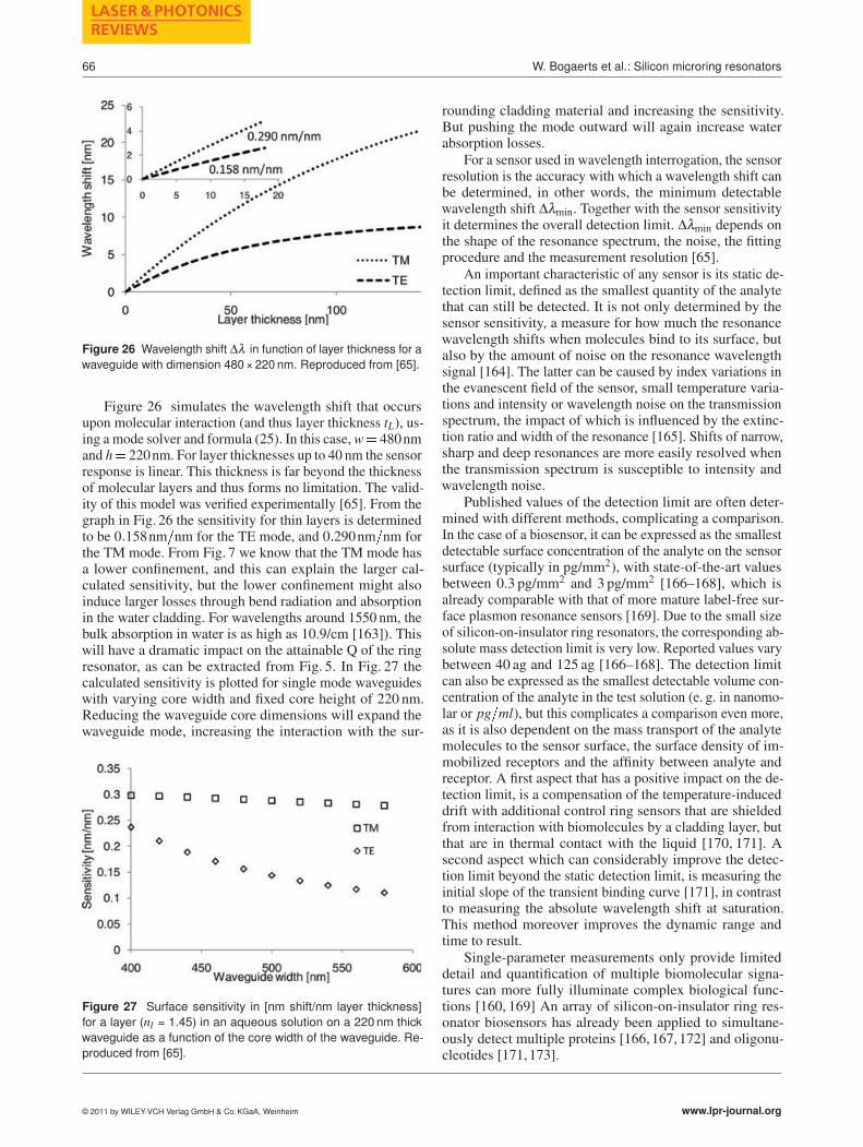
66
LASER & PHOTONICSREVIEWS
W. Bogaerts et al.: Silicon microring resonators
Figure 26 Wavelength shift Δλ in function of layer thickness for awaveguide with dimension 480 × 220 nm. Reproduced from [65].
Figure 26 simulates the wavelength shift that occursupon molecular interaction (and thus layer thickness tL), us-ing a mode solver and formula (25). In this case, w� 480nmand h� 220nm. For layer thicknesses up to 40 nm the sensorresponse is linear. This thickness is far beyond the thicknessof molecular layers and thus forms no limitation. The valid-ity of this model was verified experimentally [65]. From thegraph in Fig. 26 the sensitivity for thin layers is determinedto be 0�158nm�nm for the TE mode, and 0�290nm�nm forthe TM mode. From Fig. 7 we know that the TM mode hasa lower confinement, and this can explain the larger cal-culated sensitivity, but the lower confinement might alsoinduce larger losses through bend radiation and absorptionin the water cladding. For wavelengths around 1550 nm, thebulk absorption in water is as high as 10.9/cm [163]). Thiswill have a dramatic impact on the attainable Q of the ringresonator, as can be extracted from Fig. 5. In Fig. 27 thecalculated sensitivity is plotted for single mode waveguideswith varying core width and fixed core height of 220 nm.Reducing the waveguide core dimensions will expand thewaveguide mode, increasing the interaction with the sur-
Figure 27 Surface sensitivity in [nm shift/nm layer thickness]for a layer (nl = 1.45) in an aqueous solution on a 220 nm thickwaveguide as a function of the core width of the waveguide. Re-produced from [65].
rounding cladding material and increasing the sensitivity.But pushing the mode outward will again increase waterabsorption losses.
For a sensor used in wavelength interrogation, the sensorresolution is the accuracy with which a wavelength shift canbe determined, in other words, the minimum detectablewavelength shift Δλmin. Together with the sensor sensitivityit determines the overall detection limit. Δλmin depends onthe shape of the resonance spectrum, the noise, the fittingprocedure and the measurement resolution [65].
An important characteristic of any sensor is its static de-tection limit, defined as the smallest quantity of the analytethat can still be detected. It is not only determined by thesensor sensitivity, a measure for how much the resonancewavelength shifts when molecules bind to its surface, butalso by the amount of noise on the resonance wavelengthsignal [164]. The latter can be caused by index variations inthe evanescent field of the sensor, small temperature varia-tions and intensity or wavelength noise on the transmissionspectrum, the impact of which is influenced by the extinc-tion ratio and width of the resonance [165]. Shifts of narrow,sharp and deep resonances are more easily resolved whenthe transmission spectrum is susceptible to intensity andwavelength noise.
Published values of the detection limit are often deter-mined with different methods, complicating a comparison.In the case of a biosensor, it can be expressed as the smallestdetectable surface concentration of the analyte on the sensorsurface (typically in pg/mm2), with state-of-the-art valuesbetween 0.3 pg/mm2 and 3 pg/mm2 [166–168], which isalready comparable with that of more mature label-free sur-face plasmon resonance sensors [169]. Due to the small sizeof silicon-on-insulator ring resonators, the corresponding ab-solute mass detection limit is very low. Reported values varybetween 40 ag and 125 ag [166–168]. The detection limitcan also be expressed as the smallest detectable volume con-centration of the analyte in the test solution (e. g. in nanomo-lar or pg�ml), but this complicates a comparison even more,as it is also dependent on the mass transport of the analytemolecules to the sensor surface, the surface density of im-mobilized receptors and the affinity between analyte andreceptor. A first aspect that has a positive impact on the de-tection limit, is a compensation of the temperature-induceddrift with additional control ring sensors that are shieldedfrom interaction with biomolecules by a cladding layer, butthat are in thermal contact with the liquid [170, 171]. Asecond aspect which can considerably improve the detec-tion limit beyond the static detection limit, is measuring theinitial slope of the transient binding curve [171], in contrastto measuring the absolute wavelength shift at saturation.This method moreover improves the dynamic range andtime to result.
Single-parameter measurements only provide limiteddetail and quantification of multiple biomolecular signa-tures can more fully illuminate complex biological func-tions [160, 169] An array of silicon-on-insulator ring res-onator biosensors has already been applied to simultane-ously detect multiple proteins [166,167,172] and oligonu-cleotides [171,173].
© 2011 by WILEY-VCH Verlag GmbH & Co. KGaA, Weinheim www.lpr-journal.org

Laser Photonics Rev. 6, No. 1 (2012)
REVIEWARTICLE
67
To conclude, silicon-on-insulator ring resonators havein recent years been proven to be excellent transducers forlabel-free biosensing, comparing favorably with other label-free sensing techniques. The absence of a real need to in-tegrate sources, modulators or detectors make this a verypromising application for silicon photonics in the near fu-ture.
4.4. Active ring resonators
4.4.1. Modulators
Apart from using rings as passive devices, i. e. where theyfilter optical signals or act as a sensor, they can also be usedas an electrically actuated device. In the past few years, a lotof work has been invested by several groups in electro-opticmodulators based on ring resonators. In a ring modulator(or a modulator based on any resonator), the resonator istuned such that the operating wavelength is on the slope ofthe resonance peak. By then modulating the optical lengthof the ring, the resonance peak is shifted and the transmis-sion/reflection of the cavity is changed. This is illustratedin Fig. 28.
When using ring resonators, the most commonly ex-plored configuration is a single all-pass filter close to crit-ical coupling [140, 141]. In this configuration, there is astrong dip in the transmission spectrum of the bus wave-guide, which means that a large modulation depth ERmod
can be achieved with a relatively small shift of the ring’sresonance frequency. Obviously, the modulation is moreefficient as the slope of the resonance is steeper, i. e. whenthe ring has a higher Q and finesse. Also, it is best to operatethe modulator in the linear regime, i. e. where the slope ofthe resonance is close to a straight line. However, this im-plicates a penalty in modulation depth, and also introducesa certain IL. At higher Q, light is trapped in the ring for alonger time, and this will eventually limit the modulationspeed of the ring. For fast modulators, rings with a Q of5000–25000 are typically used.
The modulation of the effective index in the ring canbe done with different mechanisms. We already mentionedthat temperature can be used to this effect, but due to therelatively large time constants (� μs) this is not a suit-able technique for fast signals. The most commonly used
technique relies on manipulating the carrier density in thering [174]. The refractive index and the absorption of sili-con is influenced by the actual concentration of electronsand holes [113]. The most efficient mechanism in termsof magnitude is carrier injection in a p-i-n diode: The in-trinsic zone is located in the waveguide core. By forwardbiasing the diode, majority carriers are forced into the core,strongly affecting the refractive index [2, 140, 175]. How-ever, this mechanism is limited in operation speed by therecombination time of the carriers in the core (� ns). Better,one can start with a p-n diode in the core, which can bereverse-biased to increase or decrease the depletion zone inthe junction. Because the effect moves around much lesscarriers, the effect is weaker, but it is also potentially muchfaster, as it is not limited by recombination times, but ratherby the capacitance of the junction and the carrier saturationvelocity [176–179]. Manipulating the carrier density in thering will not only result in a modulation of the effectiveindex, but also of the absorption. This, in turn, will havean effect on the Q of the ring [180]. When injecting morecarriers, the Q will decrease, and thus also the slope of theresonance. In addition, changing the Q will also move thering away from critical coupling, potentially reducing theachievable modulation depth.
An advantage of ring resonators for modulation is thatthey are quite compact and can be actuated directly as alumped element, even at high speeds (10–25GHz). Also, therelatively small area limits the necessary power to modulate.Therefore, ring modulators currently hold the best trackrecord in terms of modulation energy per bit [139, 174].However, it is essential that the edge of the transmission dipis spectrally aligned with the operating wavelength of thesource. This will require good process control, but ultimatelya tuning mechanism to compensate for external influences,such as thermal variations. The modulator could be tunedby applying a bias to the modulation voltage, but as themodulation effects are typically quite small, in most casesthe tuning range will be too small. Adding thermal tuningwill help, but it can only be used in one direction (heatingnot cooling). This means that, too compensate for thermalfluctuations in the chip, the operating temperature must beset near the upper boundary of the operation specs. Thismeans continuous heating is required, which translates inan additional power consumption, negating partially the low
Figure 28 (online color at: www.lpr-journal.org)Schematic of a ring modulator. (a) Top view: thering has an active section, where a (b) diode isembedded in the cross section. (c) When biased,the transmission drops: The modulator is operatedon the slope of the ring.
www.lpr-journal.org © 2011 by WILEY-VCH Verlag GmbH & Co. KGaA, Weinheim
68
LASER & PHOTONICSREVIEWS
W. Bogaerts et al.: Silicon microring resonators
energy consumption of the ring modulator. In addition tothe spectral alignment requirements, the phase response ofthe modulated ring resonator can induce chirp in the signalif the signal bandwidth occupies a significant fraction of thering linewidth.
4.4.2. Hybrid silicon rings
Instead of incorporating an active silicon section in the ringresonator, it is also possible to heterogeneously integrateother materials in the ring cavity, especially when thosematerials can introduce gain. The most obvious materials forthat purpose are III-V semiconductors [10, 11, 181], whichare widely used for semiconductor laser diodes.
Integrating III-V material on silicon is generally doneby bonding techniques, either using direct bonding [11,182]or using an adhesive material [12, 181, 183]. A thin filmof III-V material is brought in close proximity to a siliconwaveguide, enabling evanescent coupling, and when pump-ing the III-V material, optical gain. When incorporatingsuch a gain medium in a ring, a laser cavity is formed [142].However, the transition between silicon and the gain sec-tion can introduce losses (which should be overcome by thegain section) and reflections (which can generate additionalcounterdirectional coupling). When a ring is sufficientlylarge, there can be multiple resonances within the gain band-width of the III-V material. The evenly spaced peaks (whichrequire some dispersion engineering, see Sect. 3.7) can beused to create a mode-locked laser [142]. Alternatively, onecan integrate an active region over the entire ring, usingoptical pumping to generate gain [143,184]
The same type of integration can be used to make anintegrated III-V photodetector [13]. As the detector is em-bedded in the ring resonator, it will only respond to thering resonant frequencies [143, 184, 185]. However, the lossintroduced by the detector should be sufficiently small notto quench the ring resonance too much.
Alternatively, it is possible to implement the ring en-tirely in the III-V material: The silicon bus waveguide isnow vertically coupled to the cavity. This eliminates theadditional source of loss in the ring, and also enables amuch stronger overlap of the optical mode with the gainmedium. Most implementations of this principle rely onIII-V disks rather than rings, as this facilitates the electricalcontacting [12, 143, 186, 187].
5. Summary
In this paper, we have tried to give a comprehensiveoverview of the already prolific field of silicon microringresonators. The high confinement of silicon has made itpossible to make resonators with an extremely small bendradius, footprint and a wide FSR. Especially this last prop-erty made it possible to build new functionality in siliconrings which was hitherto not possible in other materials.Over the past decade, the advances in silicon photonicshave made these rings suitable for a variety of purposes,
from filters over sensors to the use in active devices such asmodulators and lasers.
However, as we have discussed, not all aspects of siliconring resonators are perfectly understood, and the high refrac-tive index contrast of the silicon/oxide/air material systemmakes the silicon waveguides (and hence the rings) vulnera-ble to all kinds of imperfections, which in ring resonatorstranslates into a variation in resonance wavelength, qualityfactor, counterdirectional coupling and resonance splitting.
The field of silicon ring resonators is very much alive,and better understanding a technological advances will defi-nitely give us many exciting results in the coming decade,both in new physics as in valuable applications.
Acknowledgements. Part of this work was supported by theEuropean Union in the framework of the project FP7-BOOM, FP7-WaDiMOS and FP7-InTopSens, and part was supported by theBelgium Science Policy through the IAP-Photonics@be project.Wim Bogaerts and Thomas Van Vaerenbergh were supportedby the Flemish Research Foundation (FWO-Vlaanderen) for apostdoctoral fellowship and a PhD grant, respectively. Tom Claesand Katrien De Vos were supported by Flemish Institute for thePromotion of Innovation through Science and Technology (IWT)with a specialization grant. The devices measured in this paperwere fabricated in the imec CMOS pilot line through the ePIXfabMPW service, supported by the European Union through theFP7-PhotonFAB Support Action.
Received: 15 March 2011, Revised: 30 June 2011, Accepted:4 July 2011
Published online: 13 September 2011
Key words: Silicon photonics, ring resonator.
Wim Bogaerts is professor in the Photon-ics Research Group at Ghent University.He completed his studies in engineering(applied physics) at Ghent University in1998 and joined the department of infor-mation technology (INTEC) at both GhentUniversity and the Interuniversity Micro-electronics Center (IMEC) where he re-ceived his Ph. D. degree in 2004. In thephotonics research group he specialized
in the modeling, design and fabrication of nanophotonic compo-nents. Currently he coordinates the development of nanopho-tonic components in SOI in IMEC.
Peter De Heyn received the masters de-gree in photonics engineering from GhentUniversity and Vrije Universiteit Brussel(VUB), Belgium, in 2009. He is now work-ing towards a Ph. D. degree in the Photon-ics Research Group of Ghent Unversity-IMEC, Belgium. He is working towardsthe heterogeneous integration of an ultra-dense wavelength demultiplexer includingtopics as narrow linewidth ring filters and
© 2011 by WILEY-VCH Verlag GmbH & Co. KGaA, Weinheim www.lpr-journal.org
Laser Photonics Rev. 6, No. 1 (2012)
REVIEWARTICLE
69
photo-detectors. Part of his work is supported by the FP7-BOOM project of the European Union.
Thomas Van Vaerenbergh received themasters degree in applied physics fromGhent University, Belgium, in 2010. Cur-rently he works on a Ph. D. in the Pho-tonics Research Group of IMEC-GhentUniversity.
Katrien De Vos received the masters de-gree in electrical engineering from GhentUniversity, Belgium, in 2005. Until 2010she worked on a Ph. D. in the Pho-tonics Research Group of IMEC-GhentUniversity. Her research topics includedresonator-based label-free biosensors,passive SOI resonators and biocompati-ble integration with microfluidics. She at-tained her Ph. D. in 2010 and is now ac-
tive as a product manager in the pharmaceutical industry.
Shankar Kumar Selvaraja received theM. Tech. degree in Optical communicationfrom College of engineering, Anna Uni-versity, Chennai, India, in 2004 and theM. Sc. degree in Microsystems and Mi-croelectronics from University of Twente,The Netherlands, in 2005. In 2006 hejoined the Photonics Research Groupof Ghent University-imec, where he ob-tained a Ph. D. in 2011 on CMOS compat-
ible process development for Photonic integrated circuits.
Tom Claes is currently researchingsilicon-on-insulator transducers for label-free biosensing towards obtaining a Ph. D.degree at the Photonics Research Groupat the Department of Information Technol-ogy at Ghent University - IMEC, Belgiumwhere he also obtained the master de-gree in electrical engineering in 2007.
Pieter Dumon received the degree inelectrical engineering from Ghent Univer-sity, Belgium, in 2002, where he receiveda Ph. D. degree in electrical engineeringin 2007 for his work in wavelength filters insilicon photonic wires. He currently coordi-nates ePIXfab, a initiative for multi-projectwafer fabrication in photonics.
Peter Bienstman received the Degreein electrical engineering and the Ph. D.degree from Ghent University, Belgium,in 1997 and 2001, respectively. He iscurrently an Associate Professor withthe Department of Information Technol-ogy (INTEC), Ghent University. During2001/2002, he was with the Joannopou-los Research Group, Massachusetts Insti-tute of Technology (MIT). His research in-
terests include several applications of nanophotonics (biosen-sors and photonic information processing), as well as nanopho-tonics modeling.
Dries Van Thourhout received the de-gree in physical engineering and thePh. D. degree from Ghent University, Bel-gium in 1995 and 2000, respectively.From 2000 to 2002, he was with LucentTechnologies, Bell Laboratories, Craw-ford Hill, working on InPInGaAsP mono-lithically integrated devices. In 2002, hejoined the Department of InformationTechnology (INTEC), Ghent University,
continuing his work on integrated optoelectronic devices. Maininterests are heterogeneous integration by wafer bonding, intra-chip optical interconnect and WDM-devices.
Roel Baets is professor at Ghent Univer-sity. He received MSc degrees in Elec-trical Engineering from Ghent Univer-sity in 1980 and from Stanford Univer-sity in 1981. He received a Ph. D. fromGhent University in 1984. From 1984 till1989 he held a postdoctoral position atIMEC. Since 1989 he is professor in theEngineering Faculty in Ghent where hefounded the Photonics Research Group.
From 1990 till 1994 he has been part-time professor at theTechnical University of Delft and from 2004 till 2008 at the Tech-nical University of Eindhoven. Roel Baets has mainly workedin the field of integrated photonic components. He is also direc-tor of the multidisciplinary Center for Nano- and Biophotonicsin Ghent.
References
[1] W. Bogaerts, R. Baets, P. Dumon, V. Wiaux, S. Beckx,
D. Taillaert, B. Luyssaert, J. VanCampenhout, P. Bienstman,
and D. VanThourhout, J. Lightwave Technol. 23(1), 401–412 (2005).
[2] W.M. J. Green, M. Rooks, L. Sekaric, and Y. Vlasov, Opt.
Express 15(25), 17106–17113 (2007).
[3] J. Fedeli, E. Augendre, J. Hartmann, L. Vivien, P. Grosse,
V. Mazzocchi, W. Bogaerts, D. VanThourhout, and
F. Schrank, Photonics and electronics integration in the
helios project, in: Proceedings of the 7th IEEE International
Conference on Group IV Photonics (GFP), Beijing, China,
2010, pp. 356–358.
www.lpr-journal.org © 2011 by WILEY-VCH Verlag GmbH & Co. KGaA, Weinheim
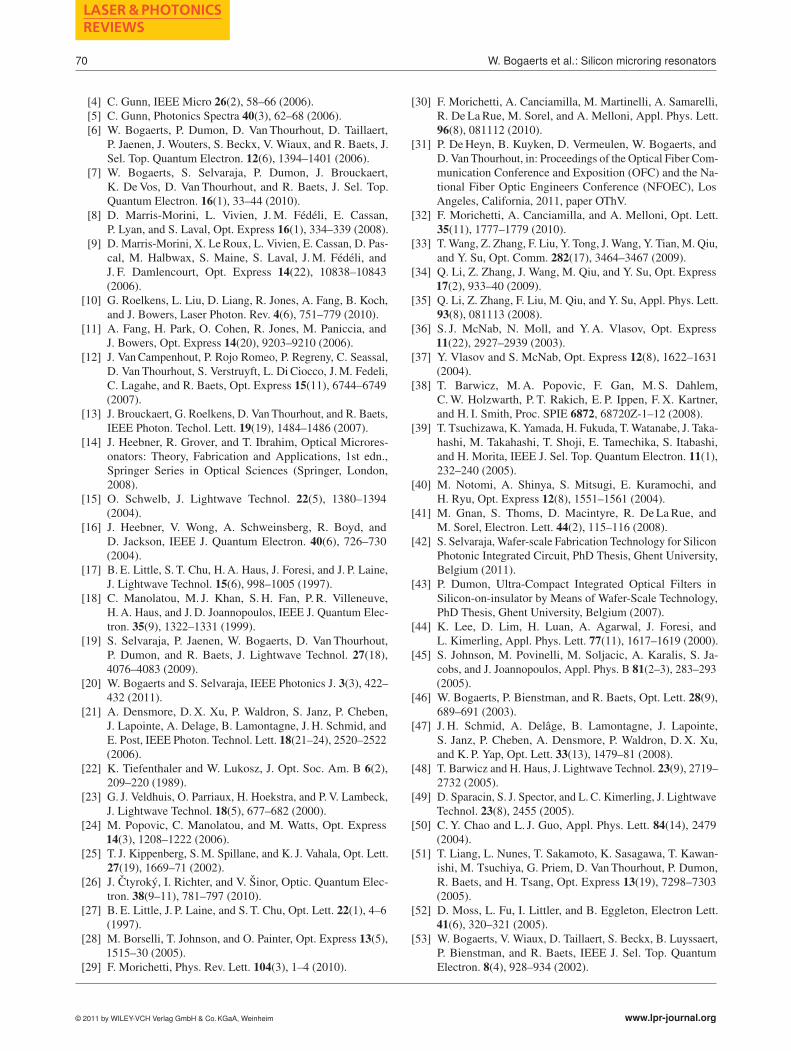
70
LASER & PHOTONICSREVIEWS
W. Bogaerts et al.: Silicon microring resonators
[4] C. Gunn, IEEE Micro 26(2), 58–66 (2006).[5] C. Gunn, Photonics Spectra 40(3), 62–68 (2006).[6] W. Bogaerts, P. Dumon, D. VanThourhout, D. Taillaert,
P. Jaenen, J. Wouters, S. Beckx, V. Wiaux, and R. Baets, J.
Sel. Top. Quantum Electron. 12(6), 1394–1401 (2006).[7] W. Bogaerts, S. Selvaraja, P. Dumon, J. Brouckaert,
K. DeVos, D. VanThourhout, and R. Baets, J. Sel. Top.
Quantum Electron. 16(1), 33–44 (2010).[8] D. Marris-Morini, L. Vivien, J.M. Fedeli, E. Cassan,
P. Lyan, and S. Laval, Opt. Express 16(1), 334–339 (2008).
[9] D. Marris-Morini, X. LeRoux, L. Vivien, E. Cassan, D. Pas-
cal, M. Halbwax, S. Maine, S. Laval, J.M. Fedeli, and
J. F. Damlencourt, Opt. Express 14(22), 10838–10843
(2006).
[10] G. Roelkens, L. Liu, D. Liang, R. Jones, A. Fang, B. Koch,
and J. Bowers, Laser Photon. Rev. 4(6), 751–779 (2010).[11] A. Fang, H. Park, O. Cohen, R. Jones, M. Paniccia, and
J. Bowers, Opt. Express 14(20), 9203–9210 (2006).[12] J. VanCampenhout, P. Rojo Romeo, P. Regreny, C. Seassal,
D. Van Thourhout, S. Verstruyft, L. Di Ciocco, J.M. Fedeli,
C. Lagahe, and R. Baets, Opt. Express 15(11), 6744–6749(2007).
[13] J. Brouckaert, G. Roelkens, D. Van Thourhout, and R. Baets,
IEEE Photon. Techol. Lett. 19(19), 1484–1486 (2007).[14] J. Heebner, R. Grover, and T. Ibrahim, Optical Microres-
onators: Theory, Fabrication and Applications, 1st edn.,
Springer Series in Optical Sciences (Springer, London,
2008).
[15] O. Schwelb, J. Lightwave Technol. 22(5), 1380–1394
(2004).
[16] J. Heebner, V. Wong, A. Schweinsberg, R. Boyd, and
D. Jackson, IEEE J. Quantum Electron. 40(6), 726–730(2004).
[17] B. E. Little, S. T. Chu, H. A. Haus, J. Foresi, and J. P. Laine,
J. Lightwave Technol. 15(6), 998–1005 (1997).
[18] C. Manolatou, M. J. Khan, S. H. Fan, P. R. Villeneuve,
H. A. Haus, and J. D. Joannopoulos, IEEE J. Quantum Elec-
tron. 35(9), 1322–1331 (1999).
[19] S. Selvaraja, P. Jaenen, W. Bogaerts, D. VanThourhout,
P. Dumon, and R. Baets, J. Lightwave Technol. 27(18),4076–4083 (2009).
[20] W. Bogaerts and S. Selvaraja, IEEE Photonics J. 3(3), 422–432 (2011).
[21] A. Densmore, D.X. Xu, P. Waldron, S. Janz, P. Cheben,
J. Lapointe, A. Delage, B. Lamontagne, J. H. Schmid, and
E. Post, IEEE Photon. Technol. Lett. 18(21–24), 2520–2522(2006).
[22] K. Tiefenthaler and W. Lukosz, J. Opt. Soc. Am. B 6(2),209–220 (1989).
[23] G. J. Veldhuis, O. Parriaux, H. Hoekstra, and P. V. Lambeck,
J. Lightwave Technol. 18(5), 677–682 (2000).[24] M. Popovic, C. Manolatou, and M. Watts, Opt. Express
14(3), 1208–1222 (2006).
[25] T. J. Kippenberg, S.M. Spillane, and K. J. Vahala, Opt. Lett.
27(19), 1669–71 (2002).
[26] J. Ctyroky, I. Richter, and V. Sinor, Optic. Quantum Elec-
tron. 38(9–11), 781–797 (2010).[27] B. E. Little, J. P. Laine, and S. T. Chu, Opt. Lett. 22(1), 4–6
(1997).
[28] M. Borselli, T. Johnson, and O. Painter, Opt. Express 13(5),1515–30 (2005).
[29] F. Morichetti, Phys. Rev. Lett. 104(3), 1–4 (2010).
[30] F. Morichetti, A. Canciamilla, M. Martinelli, A. Samarelli,
R. DeLaRue, M. Sorel, and A. Melloni, Appl. Phys. Lett.
96(8), 081112 (2010).
[31] P. DeHeyn, B. Kuyken, D. Vermeulen, W. Bogaerts, and
D. Van Thourhout, in: Proceedings of the Optical Fiber Com-
munication Conference and Exposition (OFC) and the Na-
tional Fiber Optic Engineers Conference (NFOEC), Los
Angeles, California, 2011, paper OThV.
[32] F. Morichetti, A. Canciamilla, and A. Melloni, Opt. Lett.
35(11), 1777–1779 (2010).
[33] T.Wang, Z. Zhang, F. Liu, Y. Tong, J. Wang, Y. Tian, M. Qiu,
and Y. Su, Opt. Comm. 282(17), 3464–3467 (2009).
[34] Q. Li, Z. Zhang, J. Wang, M. Qiu, and Y. Su, Opt. Express
17(2), 933–40 (2009).
[35] Q. Li, Z. Zhang, F. Liu, M. Qiu, and Y. Su, Appl. Phys. Lett.
93(8), 081113 (2008).
[36] S. J. McNab, N. Moll, and Y.A. Vlasov, Opt. Express
11(22), 2927–2939 (2003).
[37] Y. Vlasov and S. McNab, Opt. Express 12(8), 1622–1631(2004).
[38] T. Barwicz, M.A. Popovic, F. Gan, M. S. Dahlem,
C.W. Holzwarth, P. T. Rakich, E. P. Ippen, F. X. Kartner,
and H. I. Smith, Proc. SPIE 6872, 68720Z-1–12 (2008).
[39] T. Tsuchizawa, K. Yamada, H. Fukuda, T.Watanabe, J. Taka-
hashi, M. Takahashi, T. Shoji, E. Tamechika, S. Itabashi,
and H. Morita, IEEE J. Sel. Top. Quantum Electron. 11(1),232–240 (2005).
[40] M. Notomi, A. Shinya, S. Mitsugi, E. Kuramochi, and
H. Ryu, Opt. Express 12(8), 1551–1561 (2004).
[41] M. Gnan, S. Thoms, D. Macintyre, R. DeLaRue, and
M. Sorel, Electron. Lett. 44(2), 115–116 (2008).
[42] S. Selvaraja, Wafer-scale Fabrication Technology for Silicon
Photonic Integrated Circuit, PhD Thesis, Ghent University,
Belgium (2011).
[43] P. Dumon, Ultra-Compact Integrated Optical Filters in
Silicon-on-insulator by Means of Wafer-Scale Technology,
PhD Thesis, Ghent University, Belgium (2007).
[44] K. Lee, D. Lim, H. Luan, A. Agarwal, J. Foresi, and
L. Kimerling, Appl. Phys. Lett. 77(11), 1617–1619 (2000).
[45] S. Johnson, M. Povinelli, M. Soljacic, A. Karalis, S. Ja-
cobs, and J. Joannopoulos, Appl. Phys. B 81(2–3), 283–293(2005).
[46] W. Bogaerts, P. Bienstman, and R. Baets, Opt. Lett. 28(9),689–691 (2003).
[47] J. H. Schmid, A. Delage, B. Lamontagne, J. Lapointe,
S. Janz, P. Cheben, A. Densmore, P. Waldron, D.X. Xu,
and K. P. Yap, Opt. Lett. 33(13), 1479–81 (2008).
[48] T. Barwicz and H. Haus, J. Lightwave Technol. 23(9), 2719–2732 (2005).
[49] D. Sparacin, S. J. Spector, and L. C. Kimerling, J. Lightwave
Technol. 23(8), 2455 (2005).
[50] C.Y. Chao and L. J. Guo, Appl. Phys. Lett. 84(14), 2479(2004).
[51] T. Liang, L. Nunes, T. Sakamoto, K. Sasagawa, T. Kawan-
ishi, M. Tsuchiya, G. Priem, D. VanThourhout, P. Dumon,
R. Baets, and H. Tsang, Opt. Express 13(19), 7298–7303(2005).
[52] D. Moss, L. Fu, I. Littler, and B. Eggleton, Electron Lett.
41(6), 320–321 (2005).
[53] W. Bogaerts, V. Wiaux, D. Taillaert, S. Beckx, B. Luyssaert,
P. Bienstman, and R. Baets, IEEE J. Sel. Top. Quantum
Electron. 8(4), 928–934 (2002).
© 2011 by WILEY-VCH Verlag GmbH & Co. KGaA, Weinheim www.lpr-journal.org
Laser Photonics Rev. 6, No. 1 (2012)
REVIEWARTICLE
71
[54] S. Selvaraja, W. Bogaerts, and D. VanThourhout, Opt.
Comm. 284(8), 2141–2144 (2011).[55] S. K. Selvaraja, K. DeVos, W. Bogaerts, P. Bienstman,
D. VanThourhout, and R. Baets, in: 2009 IEEE LEOS An-
nual Meeting Conference Proceedings, Vols. 1 and 2 (IEEE,
New York, 2009), pp. 311–312.
[56] E. Dulkeith, F. Xia, L. Schares, W. Green, and Y. Vlasov,
Opt. Express 14(9), 3853–3863 (2006).[57] A. C. Turner, C. Manolatou, B. S. Schmidt, M. Lipson,
M.A. Foster, J. E. Sharping, and A. L. Gaeta, Opt. Express
14(10), 4357–4362 (2006).[58] P. Trinh, S. Yegnanarayanan, and B. Jalali, Electron. Lett.
31(24), 2097–2098 (1995).
[59] P. Dumon, W. Bogaerts, V. Wiaux, J. Wouters, S. Beckx,
J. VanCampenhout, D. Taillaert, B. Luyssaert, P. Bienstman,
D. VanThourhout, and R. Baets, IEEE Photon. Technol.
Lett. 16(5), 1328–1330 (2004).
[60] I. Christiaens, Vertically Coupled Microring Resonators
Fabricated with Wafer Bonding, PhD Thesis, Ghent Univer-
sity, Belgium (2005).
[61] D.X. Xu, A. Densmore, P. Waldron, J. Lapointe, E. Post,
A. Delage, S. Janz, P. Cheben, J. H. Schmid, and B. Lamon-
tagne, Opt. Express 15(6), 3149–3155 (2007).[62] C. Madsen and J. Zhao, Optical Filter design and Analysis,
Wiley Series in Microwave and Optical Engineering (John
Wiley & Sons, Inc., New York, 1999).
[63] Q. Wang, G. Farrell, and T. Freir, Opt. Comm. 259(1), 133–136 (2006).
[64] M. Popovic, Theory and Design of High-Index-Contrast
Microphotonic Circuits, PhD Thesis, MIT (2008).
[65] K. DeVos, Label-Free Silicon Photonics Biosensor Platform
with Microring Resonators, PhD Thesis, Ghent University,
Belgium (2010).
[66] M. Soltani, S. Yegnanarayanan, Q. Li, and A. Adibi, IEEE
J. Sel. Top. Quantum Electron. 46(8), 1158–1169 (2010).[67] F. Xia, L. Sekaric, and Y. Vlasov, Opt. Express 14(9), 3872–
3886 (2006).
[68] W.R. McKinnon, D.X. Xu, C. Storey, E. Post, A. Dens-
more, A. Delage, P. Waldron, J. H. Schmid, and S. Janz,
Opt. Express 17(21), 18971–18982 (2009).[69] S. K. Selvaraja, W. Bogaerts, P. Dumon, D. Van Thourhout,
and R. Baets, J. Sel. Top. Quantum Electron. 16(1), 316–324(2010).
[70] R. Boeck, N. Jaeger, N. Rouger, and L. Chrostowski, Opt.
Express 18(24), 25151–25157 (2010).[71] L. Jin, M. Li, and J. J. He, Opt. Comm. 284(1), 156–159
(2011).
[72] L. Tobing, D. Lim., P. Dumon, R. Baets, and M.K. Chin,
Appl. Phys. Lett. 92(October), 101122 (2008).
[73] S. Darmawan, L. Tobing, P. Dumon, R. Baets, and
M.K. Chin, IEEE Photon. Technol. Lett. 20(18), 1560–1562(2008).
[74] S. Darmawan, L. Tobing, P. Dumon, R. Baets, and
M.K. Chin, IEEE Photon. Technol. Lett. 20(1), 9–11
(2008).
[75] W. Bogaerts, P. Bradt, L. Vanholme, P. Bienstman, and
R. Baets, Opt. Quantum Electron. 40(11–12), 801–811(2008), 17th International Workshop on Optical Waveguide
Theory and Numerical Modelling, Eindhoven, Netherlands,
JUN 13–14, 2008.
[76] Q. Li, M. Soltani, S. Yegnanarayanan, and A. Adibi, Opt.
Express 17(4), 2247–2254 (2009).
[77] Q. Li, M. Soltani, M. Atabaki, S. Yegnanarayanan, and
A. Adibi, Opt. Express 17(26), 23474–23487 (2009).
[78] J. Heebner, R.W. Boyd, and Q.H. Park, J. Opt. Soc. Am. B
19(4), 722–731 (2002).
[79] S. Y. Cho and R. Soref, Opt. Express 16(23), 19078–19090(2008).
[80] F. Xia, L. Sekaric, and Y. Vlasov, Nature Photonics 1(1),65–71 (2007).
[81] K.O. Abrokwah, P. R. Chidambaram, and D. S. Boning,
IEEE Transactions on Semiconductor Manufacturing 20(2),77–86 (2007).
[82] C. Hedlund, H.O. Blom, and S. Berg, J. Vac. Sci. Technol.
A 12(4), 1962–1965 (1994).
[83] M. Geng, L. Jia, L. Zhang, L. Yang, P. Chen, T. Wang, and
Y. Liu, Opt. Express 17(7), 5502–5516 (2009).
[84] P. Dong, W. Qian, H. Liang, R. Shafiiha, D. Feng, G. Li,
J. Cunningham, A. Krishnamoorthy, and M. Asghari, Opt.
Express 18(19), 20298–20304 (2010).
[85] A.H. Atabaki, E. Shah Hosseini, A.A. Eftekhar, S. Yeg-
nanarayanan, and A. Adibi, Opt. Express 18(17), 18312–18323 (2010).
[86] D. Dai, L. Yang, and S. He, J. Lightwave Technol. 26(5–8),704–709 (2008).
[87] F. Gan, T. Barwicz, M.A. Popovic, M. S. Dahlem,
C.W. Holzwarth, P. T. Rakich, H. I. Smith, E. P. Ippen,
and F.X. Kartner, 2007 Photonics in Switching pp. 67–68
(2007).
[88] I. Kiyat, A. Aydinli, and N. Dagli, IEEE Photon. Technol.
Lett. 18(1–4), 364–366 (2006).
[89] J. VanCampenhout, W. Green, S. Assefa, and Y. Vlasov,
Opt. Express 17(26), 24020–24029 (2009).
[90] S.M. Lee, D. G. Cahill, and T. H. Allen, Phys. Rev. B 52(1),253 (1995).
[91] T. Coquil, E. K. Richman, N. J. Hutchinson, S. H. Tolbert,
and L. Pilon, J. Appl. Phys. 106(3), 034910–11 (2009).
[92] M.R. Watts, W.A. Zortman, D. C. Trotter, G.N. Nielson,
D. L. Luck, and R.W. Young, 2009 Conference on Lasers
and Electro-Optics and Quantum Electronics and Laser Sci-
ence Conference (Cleo/Qels 2009), Vols 1–5 pp. 812–813
(2009).
[93] J. Cunningham, I. Shubin, X. Zheng, T. Pinguet, A. Mekis,
Y. Luo, H. Thacker, G. Li, J. Yao, K. Raj, and A.V. Krish-
namoorthy, Opt. Express 18(18), 19055–19063 (2010).
[94] D. Sparacin, C.Y. Hong, L. C. Kimerling, J. Michel,
J. P. Lock, and K.K. Gleason, Opt. Lett. 30(17), 2251–2253(2005).
[95] J. Schrauwen, D. Van Thourhout, and R. Baets, Opt. Express
16(6), 3738–3743 (2008).
[96] J. Teng, P. Dumon, W. Bogaerts, H. Zhang, X. Jian, X. Han,
M. Zhao, G. Morthier, and R. Baets, Opt. Express 17(17),14627–14633 (2009).
[97] D. Dimitropoulos, R. Claps, Y. Han, and B. Jalali, in: Pro-
ceedings of the Conference on Integrated Optics – De-
vices, Materials and Technologies VII, Netherlands, CA,
2003, edited by Y. S. Sidorin and A. Tervonen, Proc. SPIE,
Vol. 4987 (2003), pp. 140–148.
[98] K. Tsia and B. Jalali, in: Proceedings of the Conference
on Silicon Photonics and Photonic Integrated Circuits II,
Brussels, Belgium, 2010, edited by G.C. Righini, Proc.
SPIE, Vol. 7719 (2010).
[99] H.K. Tsang and Y. Liu, Semicon. Sci. Technol. 23(6)(2008).
www.lpr-journal.org © 2011 by WILEY-VCH Verlag GmbH & Co. KGaA, Weinheim
72
LASER & PHOTONICSREVIEWS
W. Bogaerts et al.: Silicon microring resonators
[100] M. Dinu, F. Quochi, and H. Garcia, Appl. Phys. Lett. 82(18),2954–2956 (2003).
[101] B. Jalali, R. Claps, D. Dimitropoulos, and V. Raghunathan,
in: Silicon Photonics, Topics in Applied Physics, Vol. 94
(Springer, Berlin, Heidelberg, 2004), pp. 199–238.
[102] R. Claps, V. Raghunathan, D. Dimitropoulos, and B. Jalali,
Opt. Express 11(22), 2862–2872 (2003).[103] R. Claps, D. Dimitropoulos, and B. Jalali, Electron Lett.
38(22), 1352–1354 (2002).
[104] A. Liu, H. Rong, and M. Paniccia, Opt. Express 12(18),4261–4268 (2004).
[105] T. Liang and H. Tsang, Appl. Phys. Lett. 85(16), 3343–3345(2004).
[106] R. Jones, H. Rong, A. Liu, A. Fang, M. Paniccia, D. Hak,
and O. Cohen, Opt. Express 13(2), 519–525 (2005).[107] R. Claps, D. Dimitropoulos, V. Raghunathan, Y. Han, and
B. Jalali, Opt. Express 11(15), 1731–1739 (2003).[108] H. Rong, A. Liu, R. Jones, O. Cohen, D. Hak, R. Nico-
laescu, A. Fang, and M. Paniccia, Nature 433(7023), 292–294 (2005).
[109] O. Boyraz and B. Jalali, Opt. Express 13(3), 796–800(2005).
[110] O. Boyraz and B. Jalali, Opt. Express 12(21), 5269–5273(2004).
[111] E. Dulkeith, A. VlasovYu., X. Chen, N. Panoiu, and R. Os-
good, Opt. Express 14(12), 5524–5534 (2006).[112] R. Dekker, A. Driessen, T. Wahlbrink, C. Moormann,
J. Niehusmann, and M. Foerst, Opt. Express 14(18), 8336–8346 (2006).
[113] R. Soref and B. Bennett, J. Quantum Electron. 23(1), 123–129 (1987).
[114] H. Tsang, C. Wong, T. Liang, I. Day, S. Roberts, A. Harpin,
J. Drake, and M. Asghari, Appl. Phys. Lett. 80(3), 416–418(2002).
[115] P. Dumon, G. Priem, L. Nunes, W. Bogaerts,
D. VanThourhout, P. Bienstman, T. Liang, M. Tsuchiya,
P. Jaenen, S. Beckx, J. Wouters, and R. Baets, Japanese J.
Appl. Phys. part 1 45(8B), 6589–6602 (2006).[116] R. Jacobsen, K. Andersen, P. Borel, J. Fage-Pedersen,
L. Frandsen, O. Hansen, M. Kristensen, A. Lavrinenko,
G. Moulin, H. Ou, C. Peucheret, B. Zsigri, and A. Bjarklev,
Nature 441(7090), 199–202 (2006).[117] V. Almeida and M. Lipson, Opt. Lett. 29(20), 2387–2389
(2004).
[118] G. Priem, P. Dumon, W. Bogaerts, D. VanThourhout,
G. Morthier, and R. Baets, Opt. Express 13(23), 9623–9628(2005).
[119] Q. Xu and M. Lipson, Opt. Lett. 31(3), 341–343 (2006).[120] T. Johnson, M. Borselli, and O. Painter, Opt. Express 14(2),
817–831 (2006).
[121] B. Corcoran, C. Monat, C. Grillet, D. J. Moss, B. J. Eggleton,
T. P. White, L. O’Faolain, and T. F. Krauss, Nature Photonics
3(4), 206–210 (2009).[122] H. Fukuda, K. Yamada, T. Shoji, M. Takahashi,
T. Tsuchizawa, T. Watanabe, J. Takahashi, and S. Itabashi,
Opt. Express 13(12), 4629–4637 (2005).[123] M. Foster, A. Turner, J. Sharping, B. Schmidt, M. Lipson,
and A. Gaeta, Nature 441(7096), 960–963 (2006).[124] S. Preble, Q. Xu, and M. Lipson, Nature Photonics 1(5),
293–296 (2007).
[125] A. Turner, M. Foster, A. Gaeta, and M. Lipson, Opt. Express
16(7), 4881–4887 (2008).
[126] K. Yamada, H. Fukuda, T. Watanabe, T. Tsuchizawa, H. Shi-
nojima, T. Tanabe, M. Takahashi, and S. Itabashi, in: Pro-
ceedings of the 3rd International Conference on Group IV
Photonics, Ottawa, Canada, 2006, pp. 237–239.
[127] R. Espinola, J. Dadap, R. Osgood, S. McNab, and Y. Vlasov,
Opt. Express 13(11), 4341–4349 (2005).
[128] R. Salem, M. Foster, A. Turner, D. F. Geraghty, M. Lipson,
and A. Gaeta, Nature Photonics 2(1), 35–38 (2008).
[129] K. Yamada, T. Tsuchizawa, T. Watanabe, H. Fukuda, H. Shi-
nojima, T. Tanabe, and S. Itabashi, in: Proceedings of
the 19th Annual Meeting of the IEEE-Lasers-and-Electro-
Optics-Society, Montreal, Canada, 2006, Vols 1 and 2,
pp. 613–614.
[130] S. Clemmen, K. P. Huy, W. Bogaerts, R. G. Baets, P. Emplit,
and S. Massar, Opt. Express 17(19), 16558–16570 (2009).
[131] H. Takesue, K. I. Harada, H. Fukuda, T. Tsuchizawa,
T. Watanabe, K. Yamada, Y. Tokura, and S. I. Itabashi,
J. Nanosci. Nanotechnol. 10(3, Sp. Iss. SI), 1814–1818(2010).
[132] I.W. Hsieh, X. Chen, X. Liu, J. Dadap, N. Panoiu,
C. Y. Chou, F. Xia, W. Green, Y. Vlasov, and J. R. Osgood,
Opt. Express 15(23), 15242–15249 (2007).
[133] A. Savchenkov, A. Matsko, V. Ilchenko, I. Solomatine,
D. Seidel, and L. Maleki, Phys. Rev. Lett. 101(9) (2008).[134] M. Popovic, H. Haus, and M. Watts, in: Proceedings of the
2006 Optical Fiber Communication Conference/National
Fiber Optic Engineers Conference, Anaheim, CA, Mar. 05–
10, 2006, pp. 714–716.
[135] K. DeVos, I. Bartolozzi, D. Taillaert, W. Bogaerts, P. Bien-
stman, R. Baets, and E. Schacht, Proc. SPIE 6447(January),6447DK–1 (2007).
[136] D. Taillaert, W. Van Paepegem, J. Vlekken, and R. Baets, in:
Proc. SPIE, Vol. 6619 (2007), p. 661914.
[137] N. Yebo, P. Lommens, Z. Hens, and R. Baets, Opt. Express
18(11), 11859–11866 (2010).
[138] N. Yebo, D. Taillaert, J. Roels, D. Lahem, M. Debliquy,
D. VanThourhout, and R. Baets, IEEE Photon. Technol.
Lett. 21(14), 960–962 (2009).
[139] M. Watts, D. Trotter, R. Young, and A. Lentine, in: Proceed-
ings of the 5th IEEE International Conference on Group IV
Photonics, Sorrento, Italy, 2008, pp. 4–6.
[140] Q. Xu, S. Manipatruni, B. Schmidt, J. Shakya, and M. Lip-
son, Opt. Express 15(2), 430–436 (2007).
[141] T. Ye and X. Cai, J. Lightwave Technol. 28(11), 1615–1623(2010).
[142] B. Koch, A. Fang, O. Cohen, and J. E. Bowers, Opt. Express
15(18), 11225–11233 (2007).
[143] L. Liu, G. Roelkens, J. VanCampenhout, J. Brouckaert,
D. VanThourhout, and R. Baets, J. Nanosci. Nanotechnol.
10(3, Sp. Iss. SI), 1461–1472 (2010).
[144] J. Brouckaert, W. Bogaerts, S. Selvaraja, P. Dumon,
R. Baets, and D. VanThourhout, IEEE Photon. Technol.
Lett. 20(4), 309–311 (2008).
[145] J. Brouckaert, W. Bogaerts, P. Dumon, D. VanThourhout,
and R. Baets, J. Lightwave Technol. 25(5), 1269–1275(2007).
[146] C.W. Holzwarth, T. Barwicz, M.A. Popovic, P. T. Rakich,
E. P. Ippen, F. X. Kaertner, and H. I. Smith, J. Vac. Sci. Tech-
nol. B 24(6, Sp. Iss. SI), 3244–3247 (2006).
[147] B. Lee, B. Small, K. Bergman, Q. Xu, and M. Lipson, Opt.
Lett. 31(18), 2701–2703 (2006).
© 2011 by WILEY-VCH Verlag GmbH & Co. KGaA, Weinheim www.lpr-journal.org
Laser Photonics Rev. 6, No. 1 (2012)
REVIEWARTICLE
73
[148] M. Watts, T. Barwicz, M. Popovic, L. Socci, P. Rakich,
E. Ippen, H. Smith, and F. Kaertner, in: Proceedings of the
Conference on Lasers and Electro-Optics (CLEO), Vols 1–3,
Baltimore, MD, 2005, pp. 269–272.
[149] T. Barwicz, H. Byun, F. Gan, C.W. Holzwarth,
M.A. Popovic, P. T. Rakich, M.R. Watts, E. P. Ippen,
F. X. Kaertner, H. I. Smith, J. S. Orcutt, R. J. Ram, V. Sto-
janovic, O.O. Olubuyide, J. L. Hoyt, S. Spector, M. Geis,
M. Grein, T. Lyszczarz, and J. U. Yoon, J. Opt. Networking
6(1), 63–73 (2007).
[150] J. K. S. Poon, J. Scheuer, Y. Xu, and A. Yariv, J. Opt. Soc.
Am. B, Opt. Phys. 21(9), 1665–1673 (2004).[151] A. Melloni, A. Canciamilla, C. Ferrari, F. Morichetti,
L. O’Faolain, T. Krauss, R. DeLaRue, A. Samarelli, and
M. Sorel, IEEE Photonics J. 2(2), 181–194 (2010).[152] J. K. Poon, L. Zhu, G. DeRose, and A. Yariv, Opt. Lett.
31(4), 456–458 (2006).[153] L. Y. Mario and M.K. Chin, Opt. Express 16(3), 1796–1807
(2008).
[154] J. Yang, N.K. Fontaine, Z. Pan, A.O. Karalar, S. S. Djord-
jevic, C.X. Yang, W. Chen, S. Chu, B. E. Little, and
S. J. B. Yoo, IEEE Photon. Technol. Lett. 20(9–12), 1030–1032 (2008).
[155] A. Melloni, F. Morichetti, C. Ferrari, and M. Martinelli, Opt.
Lett. 33(20), 2389–2391 (2008).[156] F. Morichetti, A. Melloni, C. Ferrari, and M. Martinelli, Opt.
Express 16(12), 8395–8405 (2008).[157] M. S. Rasras, C.K. Madsen, M.A. Cappuzzo, E. Chen,
L. T. Gomez, E. J. Laskowski, A. Griffin, A. Wong-Foy,
A. Gasparyan, A. Kasper, J. LeGrange, and S. S. Patel,
IEEE Photon. Technol. Lett. 17(4), 834–836 (2005).[158] F. Morichetti, C. Ferrari, A. Canciamilla, and A. Melloni,
Laser and Photonics Reviews (2011).
[159] X. Fan, I. White, S. Shopoua, H. Zhu, J. Suter, and Y. Sun,
Analytica Chimica Acta 620(1–2), 8–26 (2008).
[160] A. Qavi, A. Washburn, J. Y. Byeon, and R. Bailey, Analyti-
cal and Bioanalytical Chemistry 394(1), 121–135 (2009).[161] K. DeVos, J. Girones, S. Popelka, E. Schacht, R. Baets, and
P. Bienstman, Biosens Bioelectron 24(8), 2528–33 (2009).
[162] J. Voros, Biophys. J. 87(1), 553–561 (2004).[163] K. F. Palmer and D. Williams, J. Opt. Soc. Am. 64(8), 1107–
1110 (1974).
[164] I. White and X. Fan, Opt. Express 16(2), 1020–1028 (2008).[165] J. Hu, X. Sun, A. Agarwal, and L. Kimerling, J. Opt. Soc.
Am. B 26(5), 1032–1041 (2009).[166] K. DeVos, J. Girones, T. Claes, Y. DeKoninck, S. Popelka,
E. Schacht, R. Baets, and P. Bienstman, IEEE Photonics J.
1(4), 225–235 (2009).[167] D.X. Xu, M. Vachon, A. Densmore, R. Ma, A. Delage,
S. Janz, J. Lapointe, Y. Li, G. Lopinski, D. Zhang, Q. Y. Liu,
P. Cheben, and J. H. Schmid, Opt. Lett. 35(16), 2771–2773(2010).
[168] M. Luchansky, A. Washburn, T. Martin, M. Iqbal, L. Gunn,
and R. Bailey, Biosens. Bioelectron. 26(4), 1283–1291(2010).
[169] J. Homola, Chemical Reviews 108(2), 462–493 (2008).
[170] D.X. Xu, M. Vachon, A. Densmore, R. Ma, S. Janz, A. De-
lage, J. Lapointe, P. Cheben, J. H. Schmid, E. Post, S. Mes-
saoudene, and J.M. Fedeli, Opt. Express 18(22), 22867–22879 (2010).
[171] M. Iqbal, M. Gleeson, B. Spaugh, F. Tybor, W. Gunn,
M. Hochberg, T. Baehr-Jones, R. Bailey, and L. Gunn, J.
Sel. Top. Quantum Electron. 16(3), 654–661 (2010).
[172] A. Washburn, M. Luchansky, A. Bowman, and R. Bailey,
Analy. Chem. 82(1), 69–72 (2010).
[173] A. Qavi and R. Bailey, Ang. Chem. 49(27), 4608–4611(2010).
[174] G. T. Reed, G. Mashanovich, F. Y. Gardes, and D. J. Thom-
son, Nature Photonics 4(8), 518–526 (2010).
[175] S. Manipatruni, Q. Xu, B. Schmidt, J. Shakya, and M. Lip-
son, in: Proceedings of the IEEE/LEOS 20th Annual Meet-
ing, Lake Buena Vista, Florida, 2007, pp. 537–538.
[176] S. Manipatruni, Q. Xu, and M. Lipson, Opt. Express 15(20),13035–13042 (2007).
[177] L. Liao, A. Liu, J. Basak, H. Nguyen, M. Paniccia, D. Rubin,
Y. Chetrit, R. Cohen, and N. Izhaky, Electron. Lett. 43(22)(2007).
[178] F. Gardes, G. Reed, N. Emerson, and C. Png, Opt. Express
13(22), 8845–8854 (2005).
[179] A. Liu, L. Liao, D. Rubin, H. Nguyen, B. Ciftcioglu,
Y. Chetrit, N. Izhaky, and M. Paniccia, Opt. Express 15(2),660–668 (2007).
[180] P. Dong, S. Liao, D. Feng, H. Liang, D. Zheng, R. Shafiiha,
C. C. Kung, W. Qian, G. Li, X. Zheng, A. Krishnamoorthy,
and M. Asghari, Opt. Express 17(25), 22484–22490 (2009).
[181] G. Roelkens, J. V. Campenhout, J. Brouckaert,
D.V. Thourhout, R. Baets, P. R. Romeo, P. Regreny,
A. Kazmierczak, C. Seassal, X. Letartre, G. Hollinger,
J. Fedeli, L. D. Cioccio, and C. Lagahe-Blanchard,
Materials Today 10(7–8), 36–43 (2007).
[182] M. Kostrzewa, L. D. Cioccio, M. Zussy, J. Roussin, J. Fedeli,
N. Kernevez, P. Regreny, C. Lagahe-Blanchard, and B. As-
par, Sens. Act. A, Phys. 125(2), 411–414 (2006).
[183] G. Roelkens, D. Van Thourhout, and R. Baets, Electron. Lett.
41(9), 561–562 (2005).
[184] G. Roelkens, L. Liu, D. Van Thourhout, R. Baets, R. Notzel,
F. Raineri, I. Sagnes, G. Beaudoin, and R. Raj, J. Appl. Phys.
104(3) (2008).[185] D. VanThourhout, T. Spuesens, S. Selvaraja, L. Liu,
G. Roelkens, R. Kumar, G. Morthier, P. Rojo-Romeo,
F. Mandorlo, P. Regreny, O. Raz, C. Kopp, and L. Grenouil-
let, J. Sel. Top. Quantum Electron. 16(5), 1363–1375
(2010).
[186] P. R. Romeo, J. V. Campenhout, P. Regreny, A. Kazmier-
czak, C. Seassal, X. Letartre, G. Hollinger, D. V. Thourhout,
R. Baets, J.M. Fedeli, and L. D. Cioccio, Opt. Express 14(9),3864–3871 (2006).
[187] J. VanCampenhout, L. Liu, P. Romeo, D. VanThourhout,
C. Seassal, P. Regreny, L. Di Cioccio, J.M. Fedeli, and
R. Baets, IEEE Photon. Technol. Lett. 20(16), 1345–1347(2008).
www.lpr-journal.org © 2011 by WILEY-VCH Verlag GmbH & Co. KGaA, Weinheim