Embed Size (px)
Citation preview
ECOC – Cannes, September 22, 2014
Silicon Photonics and
Skorpios’ Technology Platform
Market Watch
ECOC – Cannes - September 22, 2014
A. Viglienzoni
ECOC – Cannes, September 22, 2014
Agenda
• Preamble
• Need for Photonics and Integrated Optics
• Why Current Models Cannot Deliver on Promises
• Why CMOS Photonics
• Why Skorpios Delivers on The Promises of Silicon Photonics
• Conclusions
2
ECOC – Cannes, September 22, 2014
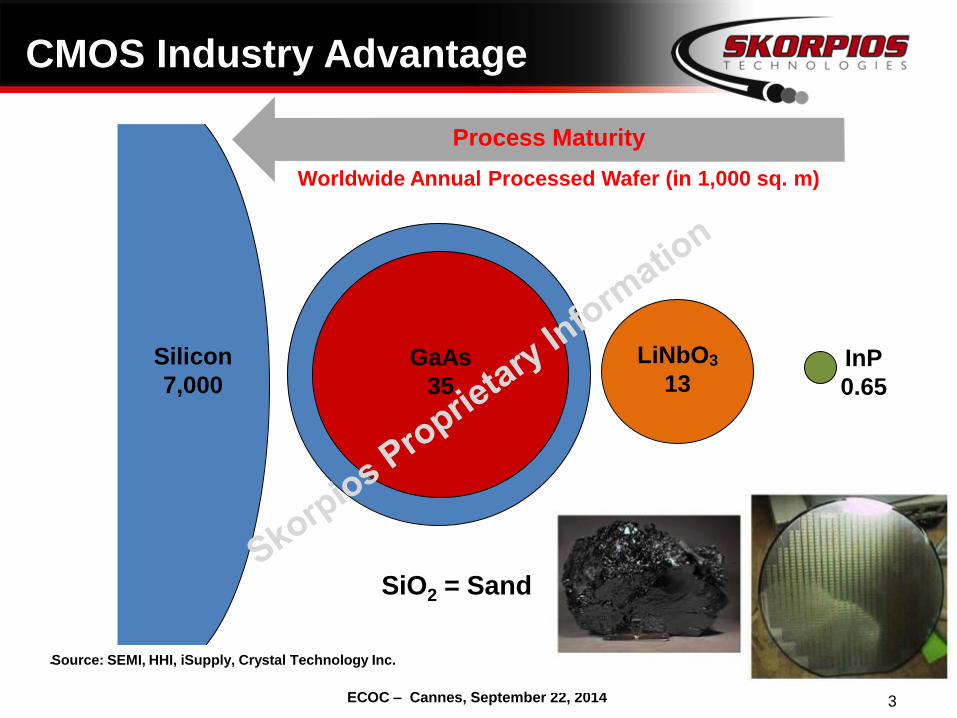
SiO2 = Sand
3
Silicon
7,000
.
Silicon
7,000
Process Maturity
Worldwide Annual Processed Wafer (in 1,000 sq. m)
Source: SEMI, HHI, iSupply, Crystal Technology Inc.
GaAs
35
LiNbO3
13 InP
0.65
CMOS Industry Advantage
ECOC – Cannes, September 22, 2014
©
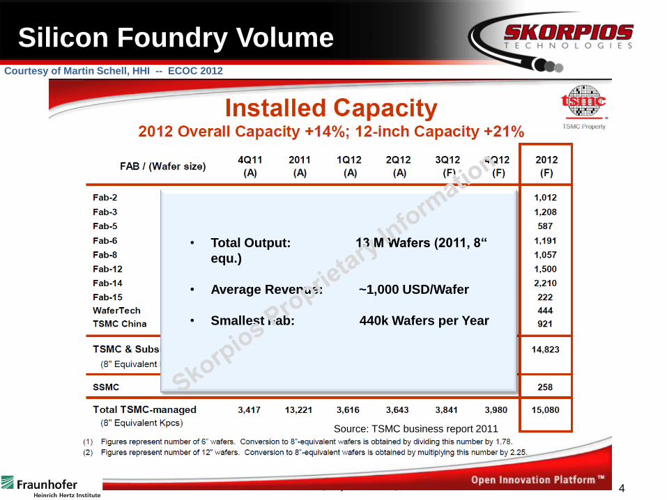
• Total Output: 13 M Wafers (2011, 8“
equ.)
• Average Revenue: ~1,000 USD/Wafer
• Smallest Fab: 440k Wafers per Year
Source: TSMC business report 2011
Courtesy of Martin Schell, HHI -- ECOC 2012
Silicon Foundry Volume
4
ECOC – Cannes, September 22, 2014
©
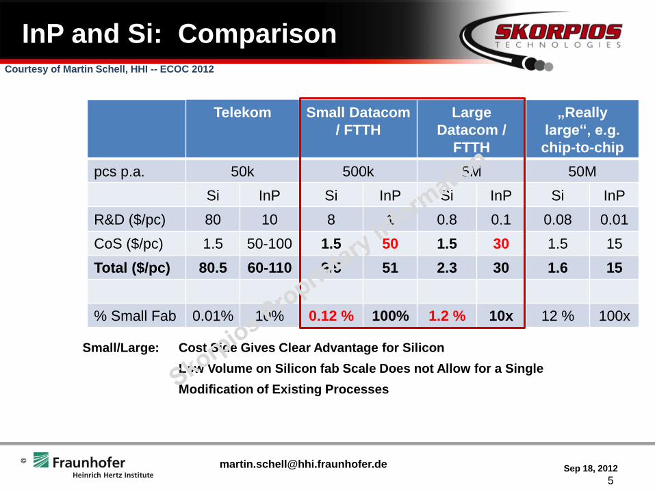
Telekom Small Datacom
/ FTTH
Large
Datacom /
FTTH
„Really
large“, e.g.
chip-to-chip
pcs p.a. 50k 500k 5M 50M
Si InP Si InP Si InP Si InP
R&D ($/pc) 80 10 8 1 0.8 0.1 0.08 0.01
CoS ($/pc) 1.5 50-100 1.5 50 1.5 30 1.5 15
Total ($/pc) 80.5 60-110 9.5 51 2.3 30 1.6 15
% Small Fab 0.01% 10% 0.12 % 100% 1.2 % 10x 12 % 100x
Small/Large: Cost Side Gives Clear Advantage for Silicon
Low Volume on Silicon fab Scale Does not Allow for a Single
Modification of Existing Processes
Sep 18, 2012 [email protected]
Courtesy of Martin Schell, HHI -- ECOC 2012
InP and Si: Comparison
5
ECOC – Cannes, September 22, 2014
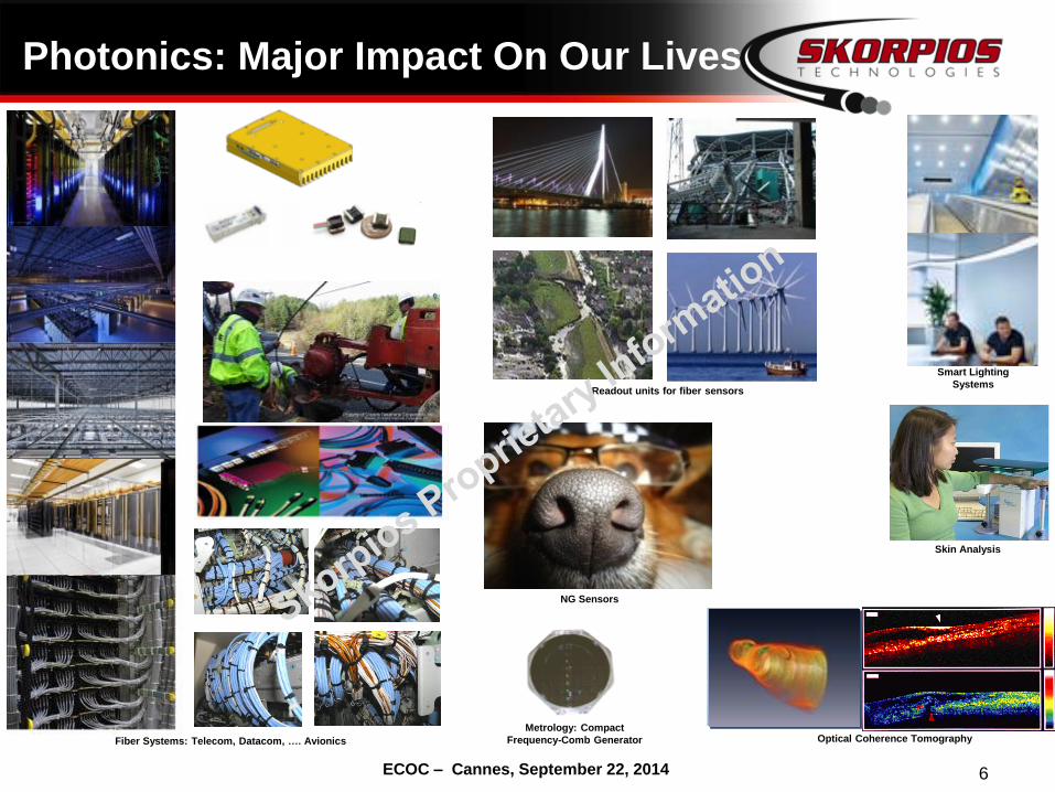
Photonics: Major Impact On Our Lives
6
Optical Coherence Tomography Metrology: Compact
Frequency-Comb Generator
Readout units for fiber sensors
Skin Analysis
Smart Lighting
Systems
Fiber Systems: Telecom, Datacom, …. Avionics
NG Sensors
ECOC – Cannes, September 22, 2014
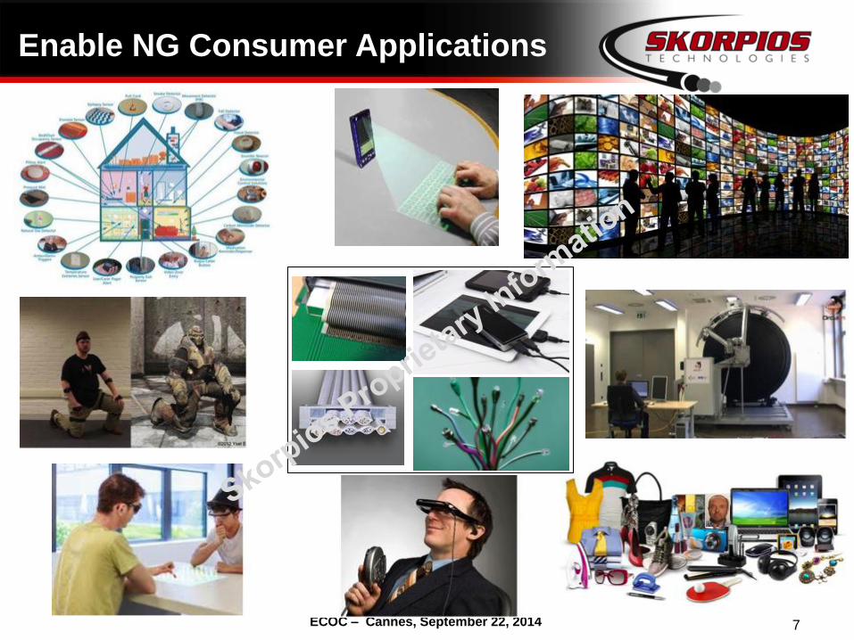
Enable NG Consumer Applications
7
ECOC – Cannes, September 22, 2014
Applications Examples Data rate
Telecom From Edge Access to Ultra Long Haul
Applications; Coherent Metro Enablement
10G, 40G, 100G, 400G Systems
Datacom Intra Data Centers (2Km+) and Inter Data
Centers (100Km); Mega Cloud SMF Duplex
100G/400G Spine-Leaf-Core Switching
40G, 100G, 400G Interconnects; Multi-
Terabit Line Cards, Dense Form-Factors
Like QSFP28
Consumer Connecting Objects e.g. Console, PC, HDTVs.
Gaming. Augmented Reality, Peer-to-Peer
5G – 50G – 100G
HPC One High Performance Computer
“Supercomputer” May Consume 40,000 AOCs
or 250,000 Mid-Board Modules
100G IB, 100 GbE
Commercial - Video Digital Signage, Digital Cinemas, Video
Recording and Studios; 4Kx2K Displays and
Recording Equipment; 100m to 1Km+
10G – 50G Interconnects
HDMI, Display Port, USB 3.0, Thunderbolt
Metrology and Sensors Measurements of Time, Temperature, Sound,
Frequency, Stress, …
Typically Low Data Rates but Using Special
Silicon Photonics Based Sensors
Medical DNA, Glucose, Molecular and Cellular Analysis,
Optical Coherence Tomography
Typically Low Data Rates but Using Special
Silicon Photonics Sensors
Military/Aerospace/
Scientific
Scientific Instruments, Optical Aircraft Networks,
Radar, Imaging and Intelligence Applications
10G, 40G, 100G, Capacity Similar to a
Small Data Center, with More Difficult
Environmental Conditions
Silicon Photonics Applications
8
ECOC – Cannes, September 22, 2014 9
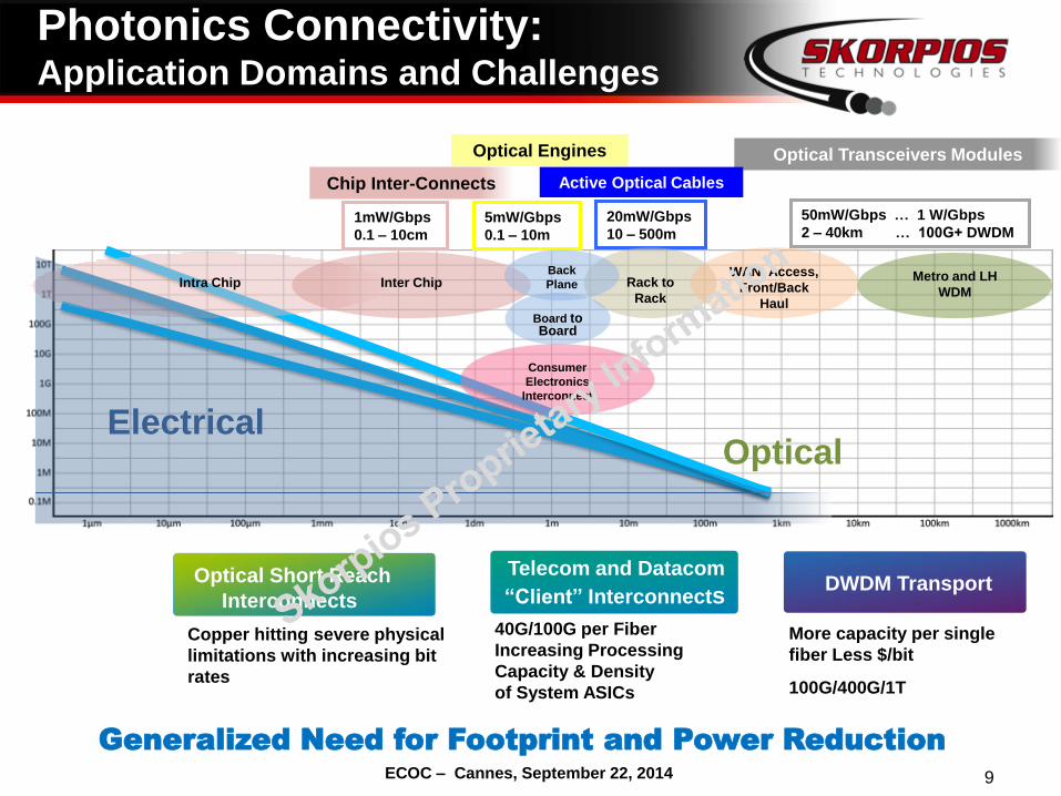
Photonics Connectivity: Application Domains and Challenges
DWDM Transport
More capacity per single
fiber Less $/bit
100G/400G/1T
Telecom and Datacom
“Client” Interconnects
40G/100G per Fiber
Increasing Processing
Capacity & Density
of System ASICs
Optical Short Reach
Interconnects
Copper hitting severe physical
limitations with increasing bit
rates
Generalized Need for Footprint and Power Reduction
Optical Transceivers Modules
Active Optical Cables
Optical Engines
Chip Inter-Connects
1mW/Gbps
0.1 – 10cm
5mW/Gbps
0.1 – 10m
20mW/Gbps
10 – 500m
50mW/Gbps … 1 W/Gbps
2 – 40km … 100G+ DWDM
Optical
Metro and LH
WDM
Rack to
Rack
WAN, Access,
Front/Back
Haul
Board to Board
Intra Chip
Inter Chip Back
Plane
Consumer
Electronics
Interconnect
Electrical
ECOC – Cannes, September 22, 2014
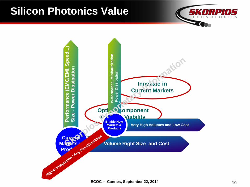
Silicon Photonics Value
Volume Right Size and Cost
Current
Markets &
Products
Pe
rfo
rma
nc
e (
EM
C/E
MI, S
pe
ed
,..)
Siz
e -
Po
we
r D
iss
ipa
tio
n
Innovate in
Current Markets
Optical Component
Industry Viability
Very High Volumes and Low Cost Enable New Markets & Products
Perf
orm
an
ce
, M
inia
turi
za
tio
n
Po
we
r D
iss
ipa
tio
n
10
ECOC – Cannes, September 22, 2014
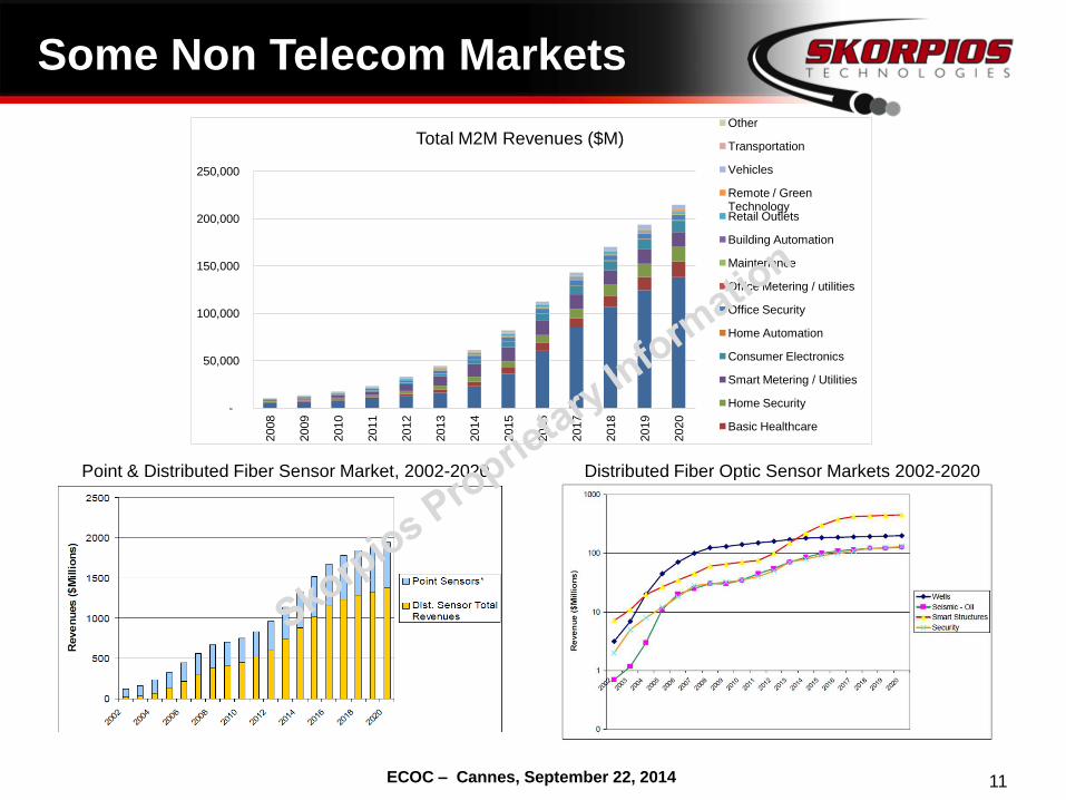
Some Non Telecom Markets
11
-
50,000
100,000
150,000
200,000
250,000
2008
2009
2010
2011
2012
2013
2014
2015
2016
2017
2018
2019
2020
Total M2M Revenues ($M) Other
Transportation
Vehicles
Remote / Green Technology Retail Outlets
Building Automation
Maintenance
Office Metering / utilities
Office Security
Home Automation
Consumer Electronics
Smart Metering / Utilities
Home Security
Basic Healthcare
Point & Distributed Fiber Sensor Market, 2002-2020 Distributed Fiber Optic Sensor Markets 2002-2020
ECOC – Cannes, September 22, 2014
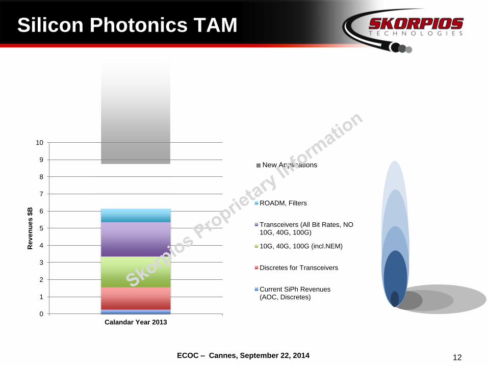
New Applications
Silicon Photonics TAM
0
1
2
3
4
5
6
7
8
9
10
Calandar Year 2013
Rev
en
ues $
B
Non Telco Applications
ROADM, Filters
Transceivers (All Bit Rates, NO 10G, 40G, 100G)
10G, 40G, 100G (incl.NEM)
Discretes for Transceivers
Current SiPh Revenues (AOC, Discretes)
12
ECOC – Cannes, September 22, 2014
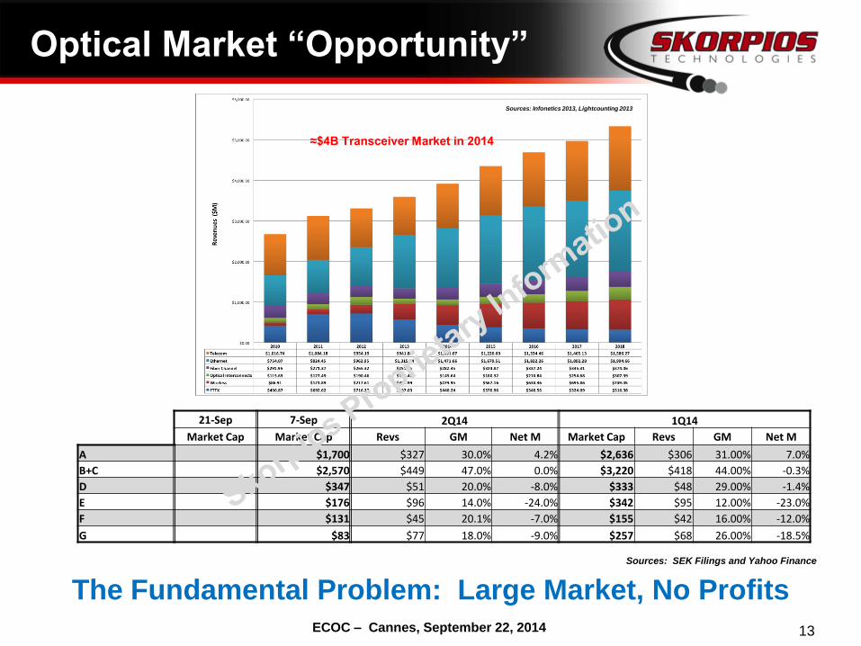
Optical Market “Opportunity”
13
Sources: SEK Filings and Yahoo Finance
The Fundamental Problem: Large Market, No Profits
Sources: Infonetics 2013, Lightcounting 2013
≈$4B Transceiver Market in 2014
21-Sep 7-Sep 2Q14 1Q14
Market Cap Market Cap Revs GM Net M Market Cap Revs GM Net M
A $1,700 $327 30.0% 4.2% $2,636 $306 31.00% 7.0%
B+C $2,570 $449 47.0% 0.0% $3,220 $418 44.00% -0.3%
D $347 $51 20.0% -8.0% $333 $48 29.00% -1.4%
E $176 $96 14.0% -24.0% $342 $95 12.00% -23.0%
F $131 $45 20.1% -7.0% $155 $42 16.00% -12.0%
G $83 $77 18.0% -9.0% $257 $68 26.00% -18.5%
ECOC – Cannes, September 22, 2014
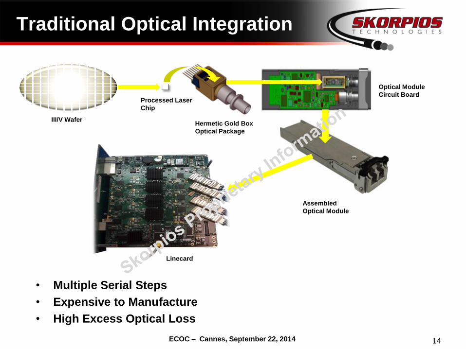
Traditional Optical Integration
14
III/V Wafer Hermetic Gold Box
Optical Package
Processed Laser
Chip
Optical Module
Circuit Board
Assembled
Optical Module
Linecard
• Multiple Serial Steps
• Expensive to Manufacture
• High Excess Optical Loss
ECOC – Cannes, September 22, 2014
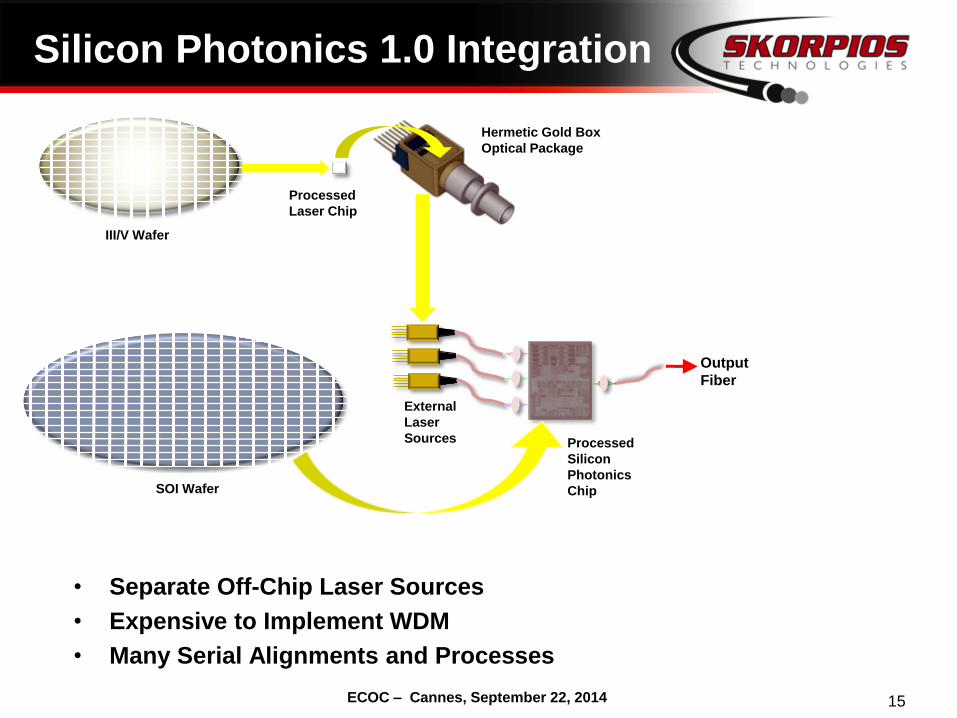
Hermetic Gold Box
Optical Package
Silicon Photonics 1.0 Integration
15
III/V Wafer
SOI Wafer
Processed
Laser Chip
Processed
Silicon
Photonics
Chip
External
Laser
Sources
Output
Fiber
• Separate Off-Chip Laser Sources
• Expensive to Implement WDM
• Many Serial Alignments and Processes
ECOC – Cannes, September 22, 2014
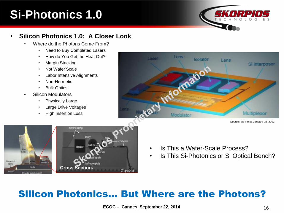
• Silicon Photonics 1.0: A Closer Look • Where do the Photons Come From?
• Need to Buy Completed Lasers
• How do You Get the Heat Out?
• Margin Stacking
• Not Wafer Scale
• Labor Intensive Alignments
• Non-Hermetic
• Bulk Optics
• Silicon Modulators
• Physically Large
• Large Drive Voltages
• High Insertion Loss
Si-Photonics 1.0
• Is This a Wafer-Scale Process?
• Is This Si-Photonics or Si Optical Bench?
Source: EE Times January 28, 2013
16
Cross Section
Silicon Photonics… But Where are the Photons?
ECOC – Cannes, September 22, 2014
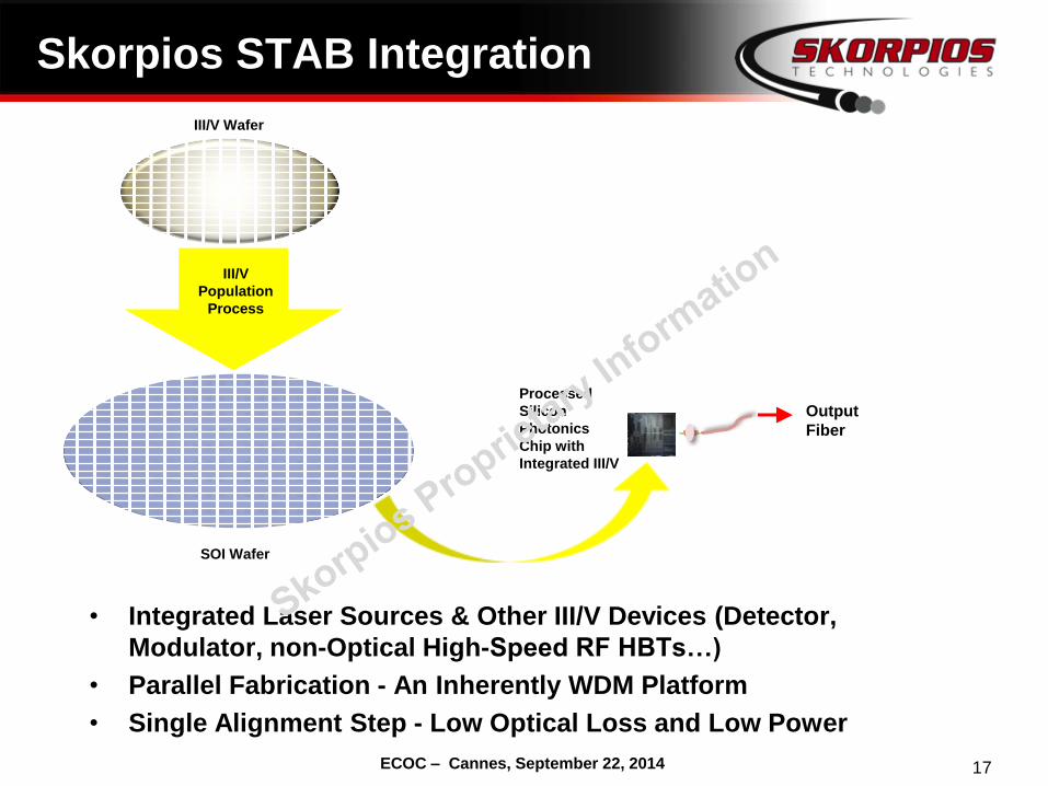
Skorpios STAB Integration
17
III/V Wafer
SOI Wafer
Output
Fiber
III/V
Population
Process
Processed
Silicon
Photonics
Chip with
Integrated III/V
• Integrated Laser Sources & Other III/V Devices (Detector,
Modulator, non-Optical High-Speed RF HBTs…)
• Parallel Fabrication - An Inherently WDM Platform
• Single Alignment Step - Low Optical Loss and Low Power
ECOC – Cannes, September 22, 2014
Si-Photonics 2.0
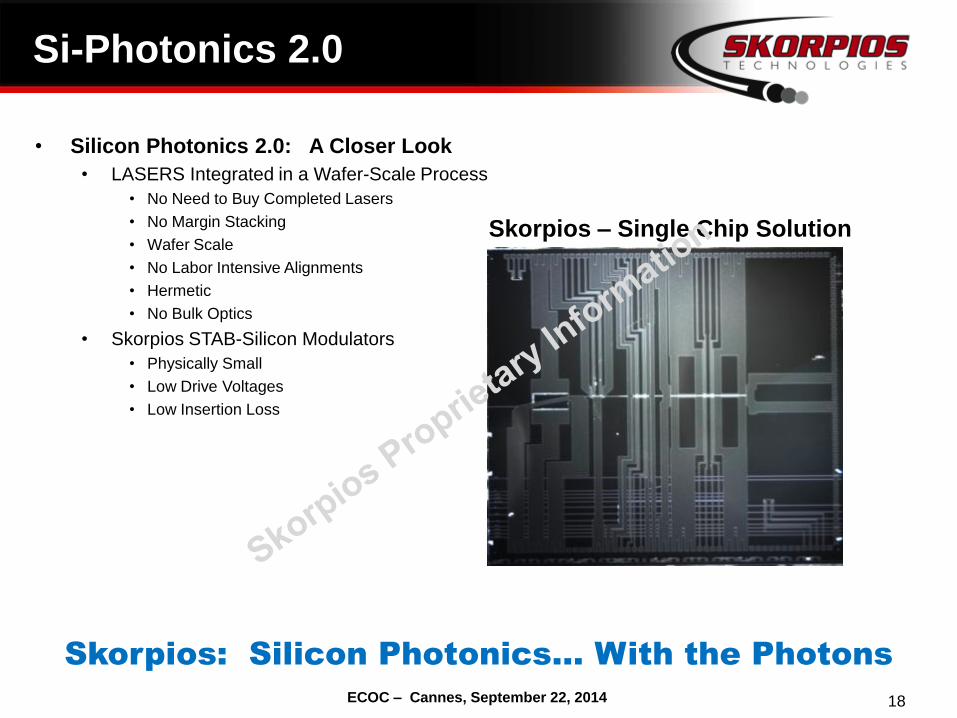
Skorpios – Single Chip Solution
• Silicon Photonics 2.0: A Closer Look
• LASERS Integrated in a Wafer-Scale Process
• No Need to Buy Completed Lasers
• No Margin Stacking
• Wafer Scale
• No Labor Intensive Alignments
• Hermetic
• No Bulk Optics
• Skorpios STAB-Silicon Modulators
• Physically Small
• Low Drive Voltages
• Low Insertion Loss
18
Skorpios: Silicon Photonics… With the Photons
ECOC – Cannes, September 22, 2014
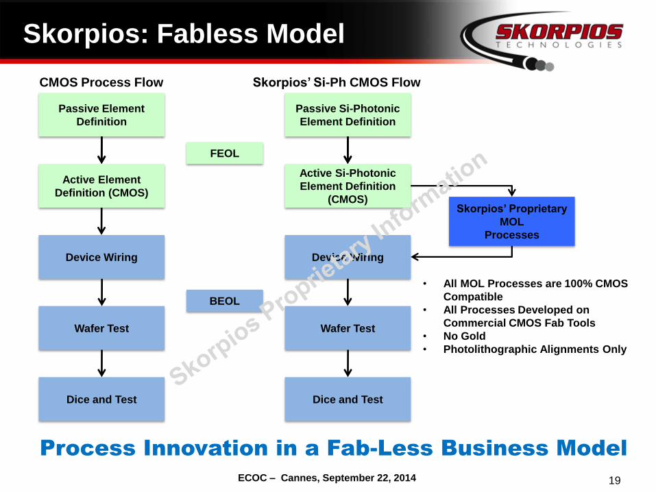
Skorpios: Fabless Model
19
Passive Element
Definition
Active Element
Definition (CMOS)
Device Wiring
Wafer Test
Dice and Test
Passive Si-Photonic
Element Definition
Active Si-Photonic
Element Definition
(CMOS)
Wafer Test
Dice and Test
CMOS Process Flow Skorpios’ Si-Ph CMOS Flow
Skorpios’ Proprietary
MOL
Processes
Device Wiring
• All MOL Processes are 100% CMOS
Compatible
• All Processes Developed on
Commercial CMOS Fab Tools
• No Gold
• Photolithographic Alignments Only
FEOL
BEOL
Process Innovation in a Fab-Less Business Model
ECOC – Cannes, September 22, 2014
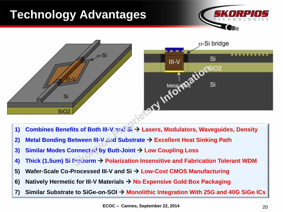
Technology Advantages
20
1) Combines Benefits of Both III-V and Si Lasers, Modulators, Waveguides, Density
2) Metal Bonding Between III-V and Substrate Excellent Heat Sinking Path
3) Similar Modes Connected by Butt-Joint Low Coupling Loss
4) Thick (1.5um) Si Platform Polarization Insensitive and Fabrication Tolerant WDM
5) Wafer-Scale Co-Processed III-V and Si Low-Cost CMOS Manufacturing
6) Natively Hermetic for III-V Materials No Expensive Gold Box Packaging
7) Similar Substrate to SiGe-on-SOI Monolithic Integration With 25G and 40G SiGe ICs
ECOC – Cannes, September 22, 2014
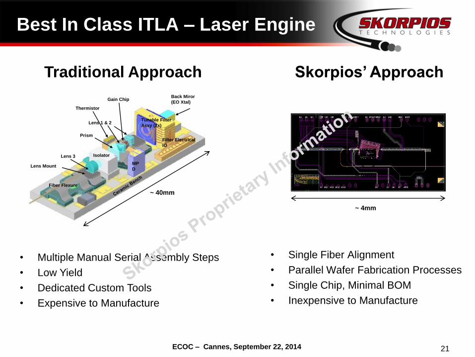
Best In Class ITLA – Laser Engine
21
• Multiple Manual Serial Assembly Steps
• Low Yield
• Dedicated Custom Tools
• Expensive to Manufacture
~ 40mm
Lens 3
Lens 1 & 2
Prism
Isolator
MP
D
Tunable Filter
Assy (2x)
Back Miror
(EO Xtal)
Fiber Flexure
Lens Mount
Thermistor
Gain Chip
Filter Electrical
IO
• Single Fiber Alignment
• Parallel Wafer Fabrication Processes
• Single Chip, Minimal BOM
• Inexpensive to Manufacture
Traditional Approach Skorpios’ Approach
~ 4mm
~ 4mm
ECOC – Cannes, September 22, 2014
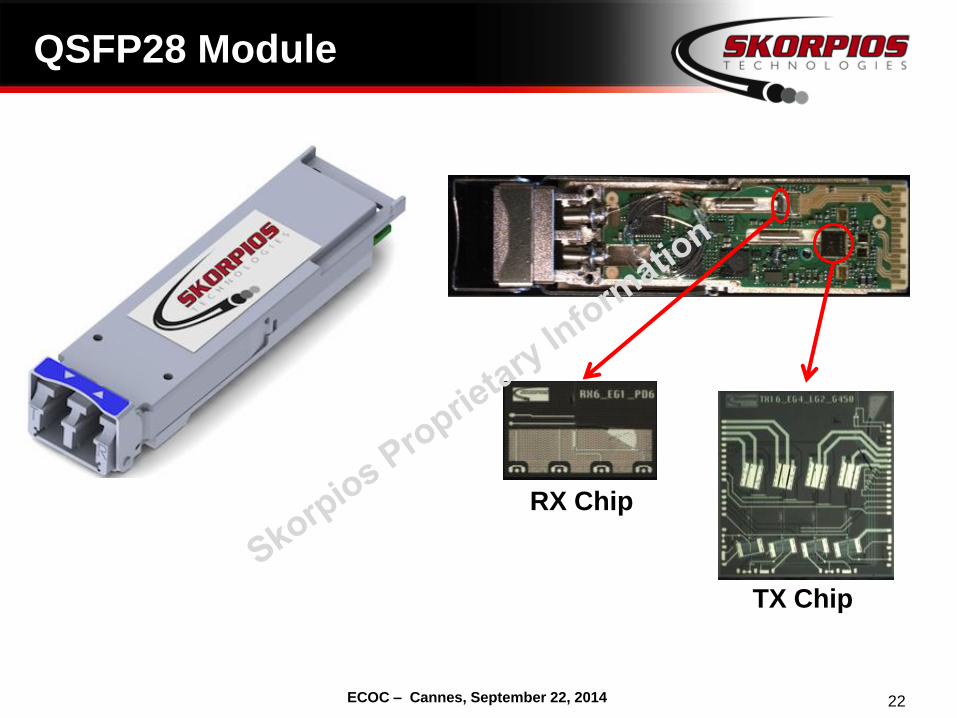
QSFP28 Module
22
RX Chip
TX Chip
ECOC – Cannes, September 22, 2014
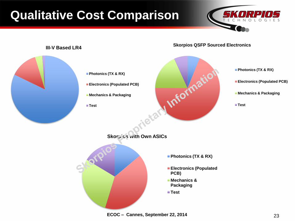
Qualitative Cost Comparison
23
III-V Based LR4
Photonics (TX & RX)
Electronics (Populated PCB)
Mechanics & Packaging
Test
Skorpios QSFP Sourced Electronics
Photonics (TX & RX)
Electronics (Populated PCB)
Mechanics & Packaging
Test
Skorpios with Own ASICs
Photonics (TX & RX)
Electronics (Populated PCB)
Mechanics & Packaging
Test
ECOC – Cannes, September 22, 2014
• Near Term Drivers for Silicon Photonics: Toolkits for Transceivers, Active Optical Cables and
Backplanes for Both Telecom and Datacom
- Optical Component Industry Cannot Keep Up With the Pace of Applications and Price/Cost Trends
- ASICs Can Process More Information Than Optical I/O’s Can Handle
• Data Rates Keep Increasing
- Electrical Links are Loss-Limited at High Data Rates
- Photonic Links Will Progressively Displace Electrical Ones
- Optical Links Have Now Entered a New Phase:
CMOS Photonics Now Competes Directly with Copper/VCSELs for Short Reach Applications: No Longer
Limited to LAN/MAN/WAN
• Volumes Growth
- Telecom: 10k-100k Units/Yr
- Datacom/HPC: >1M Units/Yr
• Silicon is the Best and Only Mature Platform:
- New Architectures Can be Enabled by Silicon Photonics
- Low Cost - Need a Process Compatible with CMOS Foundries
Skorpios Can Deliver All Such Requirements
Conclusions
24
ECOC – Cannes, September 22, 2014
Conclusions
“Future is not what it used to be.”
- Arthur C. Clarke
ECOC – Cannes, September 22, 2014
Thanks!
26