Embed Size (px)
Citation preview
Silicon photonics-wireless interface ICs for micro-/millimeter-wave fiber-wireless networks
Minsu Ko,1 Myung-Jae Lee,1 Holger Rücker,2 and Woo-Young Choi1,* 1Department of Electrical and Electronic Engineering, Yonsei University, 134 Shinchon-dong, Seodaemoon-gu,
Seoul, 120-749, Korea 2lm Technologiepark 25, IHP, 15236 Frankfurt (Oder), Germany
Abstract: We present two types of Si photonics-wireless interface (PWI) integrated circuits (ICs) realized in standard Si technology. Our PWI ICs convert optical signals into radio-frequency (RF) signals for downlink remote antenna units in fiber-wireless networks. Characterization and modeling of Si avalanche photodetectors (APDs) fabricated in two different Si technologies are carried out and used for PWI IC design. A 5-GHz RF-over-fiber PWI IC composed of APD, preamplifier, and power amplifier (PA) is fabricated in 0.18-μm CMOS technology and its performance is verified by 54-Mb/s wireless local area network data transmission. A 60-GHz baseband-over-fiber PWI IC containing APD, baseband photoreceiver, 60-GHz binary phase-shift keying (BPSK) modulator, and 60-GHz PA is realized in 0.25-μm SiGe BiCMOS technology. Error-free transmission of 1.6-Gb/s BPSK data in 60 GHz with this PWI IC is successfully achieved.
©2013 Optical Society of America
OCIS codes: (040.6040) Silicon; (060.5625) Radio frequency photonics; (250.1345) Avalanche photodiodes (APDs); (250.3140) Integrated optoelectronic circuits.
References and links
1. J. Capmany and D. Novak, “Microwave photonics combines two worlds,” Nat. Photonics 1(6), 319–330 (2007). 2. N. J. Gomes, A. Nkansah, and D. Wake, “Radio-over-MMF techniques—part I: RF to microwave frequency
systems,” J. Lightwave Technol. 26(15), 2388–2395 (2008). 3. A. M. J. Koonen and M. G. Larrodé, “Radio-over-MMF techniques—part II: microwave to millimeter-wave
systems,” J. Lightwave Technol. 26(15), 2396–2408 (2008). 4. C. Lim, A. Nirmalathas, M. Bakaul, P. Gamage, K.-L. Lee, Y. Yang, D. Novak, and R. Waterhouse, “Fiber-
wireless networks and subsystem technologies,” J. Lightwave Technol. 28(4), 390–405 (2010). 5. M. Maier, N. Ghazisaidi, and M. Reisslein, “The audacity of fiber-wireless (FiWi) networks,” in Proceedings of
ICST International Conference on Access Networks (AccessNets) (ICST, 2008), pp. 16–35. 6. L. Liao, A. Liu, D. Rubin, J. Basak, Y. Chetrit, H. Nguyen, R. Cohen, N. Izhaky, and M. Paniccia, “40 Gbit/s
silicon optical modulator for high-speed applications,” Electron. Lett. 43(22), 1196–1197 (2007). 7. G. Li, X. Zheng, H. Thacker, J. Yao, Y. Luo, I. Shubin, K. Raj, J. E. Cunningham, and A. V. Krishnamoorthy,
“40 Gb/s thermally tunable CMOS ring modulator,” in Proceedings of 2012 IEEE 9th International Conference on Group IV Photonics (GFP) (IEEE, 2012), pp. 1–3.
8. L. Vivien, D. Marris-Morini, J. Mangeney, P. Crozat, E. Cassan, S. Laval, J.-M. Fédéli, J. F. Damlencourt, and Y. Lecunff, “42 GHz waveguide germanium-on-silicon vertical PIN photodetector,” in Proceedings of 2008 IEEE 5th International Conference on Group IV Photonics (GFP) (IEEE, 2008), pp. 185–187.
9. S. Assefa, F. Xia, S. W. Bedell, Y. Zhang, T. Topuria, P. M. Rice, and Y. A. Vlasov, “CMOS-integrated 40GHz germanium waveguide photodetector for on-chip optical interconnects,” in Optical Fiber Communication Conference (OSA, 2009), paper OMR4.
10. E. Seok, D. Shim, C. Mao, R. Han, S. Sankaran, C. Cao, W. Knap, and K. O. Kenneth, “Progress and challenges towards terahertz CMOS integrated circuits,” IEEE J. Solid-State Circuits 45(8), 1554–1564 (2010).
11. M. Ko, J.-Y. Kim, M.-J. Lee, H. Rücker, and W.-Y. Choi, “A silicon balanced subharmonic optoelectronic mixer for 60-GHz fiber-wireless downlink application,” IEEE Photon. Technol. Lett. 23(23), 1805–1807 (2011).
12. R. Soref, “The past, present, and future of silicon photonics,” IEEE J. Sel. Top. Quantum Electron. 12(6), 1678–1687 (2006).
13. M. Ko, J.-M. Lee, M.-J. Lee, and W.-Y. Choi, “A 5-GHz CMOS integrated radio-over-fiber receiver,” presented at the 8th Asia-Pacific Microwave Photonics Conference (APMP 2013), Gwangju, Korea, 22–24 Apr. 2013.
14. M. Ko, J.-S. Youn, M.-J. Lee, K.-C. Choi, H. Rücker, and W.-Y. Choi, “Silicon photonics-wireless interface IC for 60-GHz wireless link,” IEEE Photon. Technol. Lett. 24(13), 1112–1114 (2012).
#191763 - $15.00 USD Received 4 Jun 2013; revised 8 Aug 2013; accepted 8 Aug 2013; published 23 Sep 2013(C) 2013 OSA 23 September 2013 | Vol. 21, No. 19 | DOI:10.1364/OE.21.022962 | OPTICS EXPRESS 22962
15. M.-J. Lee and W.-Y. Choi, “Area-dependent photodetection frequency response characterization of silicon avalanche photodetectors fabricated with standard CMOS technology,” IEEE Trans. Electron. Dev. 60(3), 998–1004 (2013).
16. J.-S. Youn, M.-J. Lee, K.-Y. Park, W.-Y. Choi, and H. Rücker, “Bit-error rate analysis of integrated optoelectronic receiver,” in Proceedings of Photonics Global Conference (PGC) (IEEE, 2012), pp. 1–3.
17. M.-J. Lee, H.-S. Kang, and W.-Y. Choi, “Equivalent circuit model for Si avalanche photodetectors fabricated in standard CMOS process,” IEEE Electron Device Lett. 29(10), 1115–1117 (2008).
18. A. Leven, R. Reuter, and Y. Baeyens, “Unified analytical expressions for transimpedance and equivalent input noise current of optical receivers,” IEEE Trans. Microw. Theory Tech. 48(10), 1701–1706 (2000).
19. B. Heinemann, R. Barth, D. Knoll, H. Rücker, B. Tillack, and W. Winkler, “High-performance BiCMOS technologies without epitaxially-buried subcollectors and deep trenches,” Semicond. Sci. Technol. 22(1), S153–S157 (2007).
20. G. S. Sahota and C. J. Persico, “High dynamic range variable-gain amplifier for CDMA wireless applications,” in Proceedings of IEEE International Solid-State Circuits Conference (IEEE, 1997), pp. 374–375.
21. K.-C. Choi, M. Ko, D. Kim, and W.-Y. Choi, “Demonstration of 60-GHz link using a 1.6-Gb/s mixed-mode BPSK demodulator,” IEICE Trans. Electron. E93-C(12), 1704–1707 (2010).
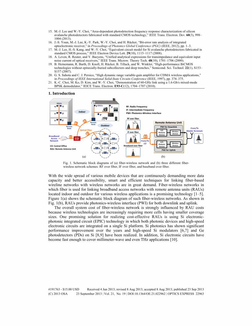
1. Introduction
(b)(a)
PWI for Downlink
PWI for Uplink
fRF
RF over fiber
fIF
IF over fiber
Baseband over fiber
fRFFrom/ToCO
From/ToMobile Terminals
E/OPhotonicDevices
WirelessDevices
O/EPhotonicDevices
WirelessDevices
Remote Antenna Unit
RF: Radio FrequencyIF: Intermediate FrequencyPWI: Photonics-Wireless Interface
RAUsRAUs
RAU
RAU
RAU
RAU
RAU
RAU
RAU
BroadbandAccess
NetworkCO
Indoor
OutdoorRemoteNode
RemoteNode
Optical Fiber
CO: Central OfficeRAU: Remote Antenna Unit
Fig. 1. Schematic block diagrams of (a) fiber-wireless network and (b) three different fiber-wireless network schemes: RF over fiber, IF over fiber, and baseband over fiber.
With the wide spread of various mobile devices that are continuously demanding more data capacity and better accessibility, smart and efficient techniques for linking fiber-based wireline networks with wireless networks are in great demand. Fiber-wireless networks in which fiber is used for linking broadband access networks with remote antenna units (RAUs) located indoor and outdoor for various wireless applications is a promising technology [1–5]. Figure 1(a) shows the schematic block diagram of such fiber-wireless networks. As shown in Fig. 1(b), RAUs provide photonics-wireless interface (PWI) for both downlink and uplink.
The overall system cost of fiber-wireless network is strongly influenced by RAU costs because wireless technologies are increasingly requiring more cells having smaller coverage sizes. One promising solution for realizing cost-effective RAUs is using Si electronic-photonic integrated circuit (EPIC) technology in which both photonic devices and high-speed electronic circuits are integrated on a single Si platform. Si photonics has shown significant performance improvement over the years and high-speed Si modulators [6,7] and Ge photodetectors (PDs) on Si [8,9] have been realized. In addition, Si electronic circuits have become fast enough to cover millimeter-wave and even THz applications [10].
#191763 - $15.00 USD Received 4 Jun 2013; revised 8 Aug 2013; accepted 8 Aug 2013; published 23 Sep 2013(C) 2013 OSA 23 September 2013 | Vol. 21, No. 19 | DOI:10.1364/OE.21.022962 | OPTICS EXPRESS 22963
LightSource
MOD
DEMOD
PD
EOM
fRF
Baseband over fiber
(c)
(a)
fRF
RF over fiber PD
EOM
LightSource
fRF
(b)
PD: PhotodetectorEOM: Electrooptic ModulatorMOD: ModulatorDEMOD: Demodulator
fIF
IF over fiber
+O/E Mixer
LightSource
PD
EOM
fRF
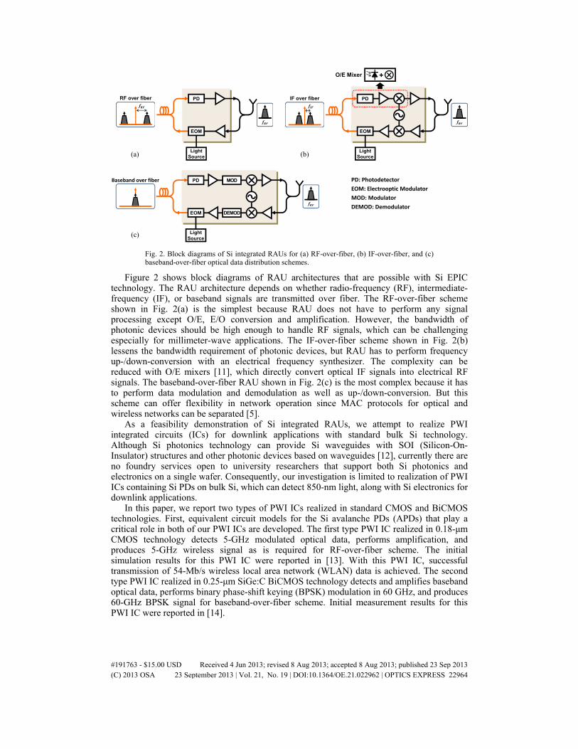
Fig. 2. Block diagrams of Si integrated RAUs for (a) RF-over-fiber, (b) IF-over-fiber, and (c) baseband-over-fiber optical data distribution schemes.
Figure 2 shows block diagrams of RAU architectures that are possible with Si EPIC technology. The RAU architecture depends on whether radio-frequency (RF), intermediate-frequency (IF), or baseband signals are transmitted over fiber. The RF-over-fiber scheme shown in Fig. 2(a) is the simplest because RAU does not have to perform any signal processing except O/E, E/O conversion and amplification. However, the bandwidth of photonic devices should be high enough to handle RF signals, which can be challenging especially for millimeter-wave applications. The IF-over-fiber scheme shown in Fig. 2(b) lessens the bandwidth requirement of photonic devices, but RAU has to perform frequency up-/down-conversion with an electrical frequency synthesizer. The complexity can be reduced with O/E mixers [11], which directly convert optical IF signals into electrical RF signals. The baseband-over-fiber RAU shown in Fig. 2(c) is the most complex because it has to perform data modulation and demodulation as well as up-/down-conversion. But this scheme can offer flexibility in network operation since MAC protocols for optical and wireless networks can be separated [5].
As a feasibility demonstration of Si integrated RAUs, we attempt to realize PWI integrated circuits (ICs) for downlink applications with standard bulk Si technology. Although Si photonics technology can provide Si waveguides with SOI (Silicon-On-Insulator) structures and other photonic devices based on waveguides [12], currently there are no foundry services open to university researchers that support both Si photonics and electronics on a single wafer. Consequently, our investigation is limited to realization of PWI ICs containing Si PDs on bulk Si, which can detect 850-nm light, along with Si electronics for downlink applications.
In this paper, we report two types of PWI ICs realized in standard CMOS and BiCMOS technologies. First, equivalent circuit models for the Si avalanche PDs (APDs) that play a critical role in both of our PWI ICs are developed. The first type PWI IC realized in 0.18-μm CMOS technology detects 5-GHz modulated optical data, performs amplification, and produces 5-GHz wireless signal as is required for RF-over-fiber scheme. The initial simulation results for this PWI IC were reported in [13]. With this PWI IC, successful transmission of 54-Mb/s wireless local area network (WLAN) data is achieved. The second type PWI IC realized in 0.25-μm SiGe:C BiCMOS technology detects and amplifies baseband optical data, performs binary phase-shift keying (BPSK) modulation in 60 GHz, and produces 60-GHz BPSK signal for baseband-over-fiber scheme. Initial measurement results for this PWI IC were reported in [14].
#191763 - $15.00 USD Received 4 Jun 2013; revised 8 Aug 2013; accepted 8 Aug 2013; published 23 Sep 2013(C) 2013 OSA 23 September 2013 | Vol. 21, No. 19 | DOI:10.1364/OE.21.022962 | OPTICS EXPRESS 22964
This paper is organized as follows. Section 2 gives the device characteristics and the equivalent circuit model of Si APD. Section 3 discusses the design, simulation, and WLAN data transmission results of 5-GHz PWI IC. Section 4 gives detailed circuit description and measurement results of 60-GHz PWI IC. Finally, Section 5 concludes this paper.
2. Si APDs
2.1 Device description of Si APD
(b)(a)
850-nmLight Lensed
Fiber
N-well Bias Port(DC: VPD)
(DC: GND)P+ Signal Port
−
+ Reverse bias
Photocurrent
Light
P-substrate
N+N+STI
P+P+ P+
N-well
N-well port
P+
port
P+
Penetration depth> 10 μm
10 μm
Fig. 3. (a) Cross-section view and (b) port configuration of APD.
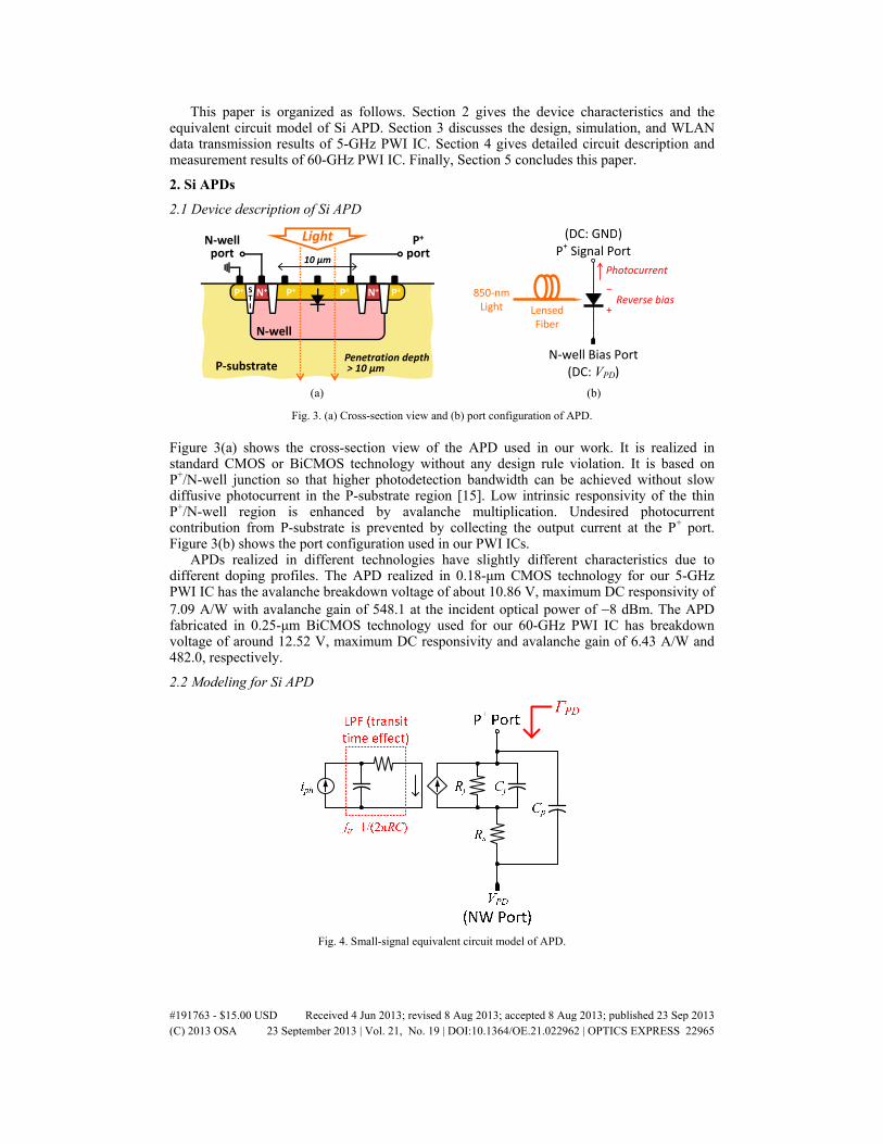
Figure 3(a) shows the cross-section view of the APD used in our work. It is realized in standard CMOS or BiCMOS technology without any design rule violation. It is based on P+/N-well junction so that higher photodetection bandwidth can be achieved without slow diffusive photocurrent in the P-substrate region [15]. Low intrinsic responsivity of the thin P+/N-well region is enhanced by avalanche multiplication. Undesired photocurrent contribution from P-substrate is prevented by collecting the output current at the P+ port. Figure 3(b) shows the port configuration used in our PWI ICs.
APDs realized in different technologies have slightly different characteristics due to different doping profiles. The APD realized in 0.18-μm CMOS technology for our 5-GHz PWI IC has the avalanche breakdown voltage of about 10.86 V, maximum DC responsivity of 7.09 A/W with avalanche gain of 548.1 at the incident optical power of −8 dBm. The APD fabricated in 0.25-μm BiCMOS technology used for our 60-GHz PWI IC has breakdown voltage of around 12.52 V, maximum DC responsivity and avalanche gain of 6.43 A/W and 482.0, respectively.
2.2 Modeling for Si APD
Fig. 4. Small-signal equivalent circuit model of APD.
#191763 - $15.00 USD Received 4 Jun 2013; revised 8 Aug 2013; accepted 8 Aug 2013; published 23 Sep 2013(C) 2013 OSA 23 September 2013 | Vol. 21, No. 19 | DOI:10.1364/OE.21.022962 | OPTICS EXPRESS 22965
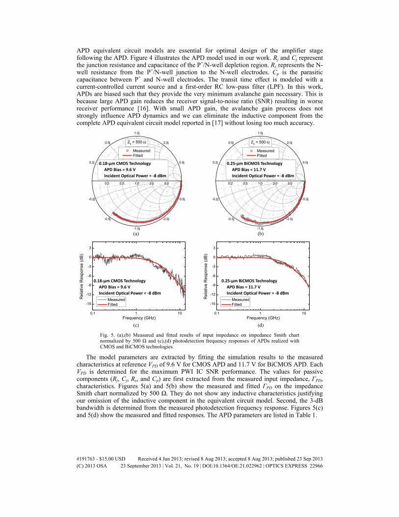
APD equivalent circuit models are essential for optimal design of the amplifier stage following the APD. Figure 4 illustrates the APD model used in our work. Rj and Cj represent the junction resistance and capacitance of the P+/N-well depletion region. Rs represents the N-well resistance from the P+/N-well junction to the N-well electrodes. Cp is the parasitic capacitance between P+ and N-well electrodes. The transit time effect is modeled with a current-controlled current source and a first-order RC low-pass filter (LPF). In this work, APDs are biased such that they provide the very minimum avalanche gain necessary. This is because large APD gain reduces the receiver signal-to-noise ratio (SNR) resulting in worse receiver performance [16]. With small APD gain, the avalanche gain process does not strongly influence APD dynamics and we can eliminate the inductive component from the complete APD equivalent circuit model reported in [17] without losing too much accuracy.
0.2 0.5 1.0 2.0 5.0
-0.2j
0.2j
-0.5j
0.5j
-1.0j
1.0j
-2.0j
2.0j
-5.0j
5.0j
Measured Fitted
Z0 = 500 Ω
0.2 0.5 1.0 2.0 5.0
-0.2j
0.2j
-0.5j
0.5j
-1.0j
1.0j
-2.0j
2.0j
-5.0j
5.0j
Measured Fitted
Z0 = 500 Ω
0.1 1 10
-15
-12
-9
-6
-3
0
3
Re
lativ
e R
esp
onse
(dB
)
Frequency (GHz)
Measured Fitted
0.1 1 10
-15
-12
-9
-6
-3
0
3
Re
lativ
e R
esp
onse
(dB
)
Frequency (GHz)
Measured Fitted
(d)(c)
(b)(a)
0.18-μm CMOS TechnologyAPD Bias = 9.6 VIncident Optical Power = -8 dBm
0.25-μm BiCMOS TechnologyAPD Bias = 11.7 VIncident Optical Power = -8 dBm
0.18-μm CMOS TechnologyAPD Bias = 9.6 VIncident Optical Power = -8 dBm
0.25-μm BiCMOS TechnologyAPD Bias = 11.7 VIncident Optical Power = -8 dBm
Fig. 5. (a),(b) Measured and fitted results of input impedance on impedance Smith chart normalized by 500 Ω and (c),(d) photodetection frequency responses of APDs realized with CMOS and BiCMOS technologies.
The model parameters are extracted by fitting the simulation results to the measured characteristics at reference VPD of 9.6 V for CMOS APD and 11.7 V for BiCMOS APD. Each VPD is determined for the maximum PWI IC SNR performance. The values for passive components (Rj, Cj, Rs, and Cp) are first extracted from the measured input impedance, ΓPD, characteristics. Figures 5(a) and 5(b) show the measured and fitted ΓPD on the impedance Smith chart normalized by 500 Ω. They do not show any inductive characteristics justifying our omission of the inductive component in the equivalent circuit model. Second, the 3-dB bandwidth is determined from the measured photodetection frequency response. Figures 5(c) and 5(d) show the measured and fitted responses. The APD parameters are listed in Table 1.
#191763 - $15.00 USD Received 4 Jun 2013; revised 8 Aug 2013; accepted 8 Aug 2013; published 23 Sep 2013(C) 2013 OSA 23 September 2013 | Vol. 21, No. 19 | DOI:10.1364/OE.21.022962 | OPTICS EXPRESS 22966
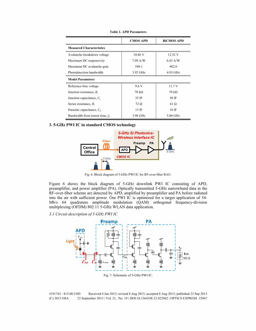
Table 1. APD Parameters
CMOS APD BiCMOS APD
Measured Characteristics
Avalanche breakdown voltage 10.86 V 12.52 V
Maximum DC responsivity 7.09 A/W 6.43 A/W
Maximum DC avalanche gain 548.1 482.0
Photodetection bandwidth 3.92 GHz 4.93 GHz
Model Parameters
Reference bias voltage 9.6 V 11.7 V
Junction resistance, Rj 70 kΩ 70 kΩ
Junction capacitance, Cj 35 fF 30 fF
Series resistance, Rs 72 Ω 61 Ω
Parasitic capacitance, Cp 13 fF 10 fF
Bandwidth from transit time, ftr 3.98 GHz 5.00 GHz
3. 5-GHz PWI IC in standard CMOS technology
PAPreamp
5 GHz
5-GHz Si Photonics-Wireless Interface IC
APD
Fiber
CentralOffice
5 GHzCMOS IC
Fig. 6. Block diagram of 5-GHz PWI IC for RF-over-fiber RAU.
Figure 6 shows the block diagram of 5-GHz downlink PWI IC consisting of APD, preamplifier, and power amplifier (PA). Optically transmitted 5-GHz narrowband data in the RF-over-fiber scheme are detected by APD, amplified by preamplifier and PA before radiated into the air with sufficient power. Our PWI IC is optimized for a target application of 54-Mb/s 64 quadrature amplitude modulation (QAM) orthogonal frequency-division multiplexing (OFDM) 802.11 5-GHz WLAN data application.
3.1 Circuit description of 5-GHz PWI IC
Fig. 7. Schematic of 5-GHz PWI IC.
#191763 - $15.00 USD Received 4 Jun 2013; revised 8 Aug 2013; accepted 8 Aug 2013; published 23 Sep 2013(C) 2013 OSA 23 September 2013 | Vol. 21, No. 19 | DOI:10.1364/OE.21.022962 | OPTICS EXPRESS 22967
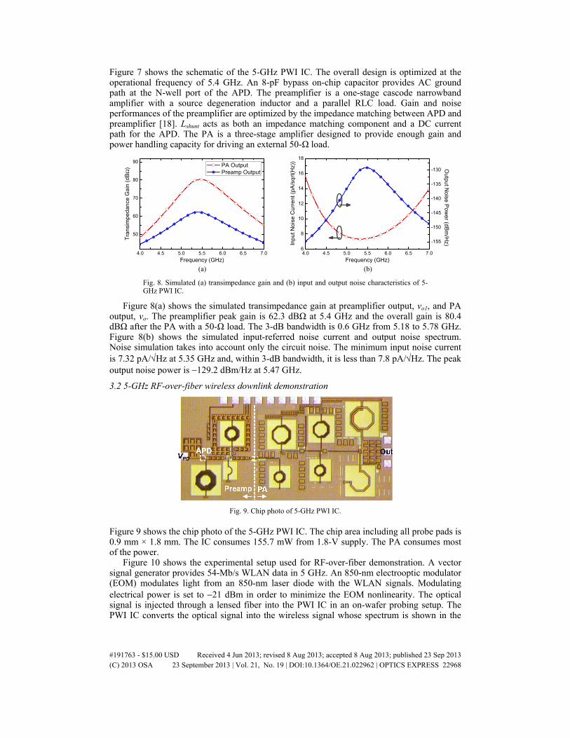
Figure 7 shows the schematic of the 5-GHz PWI IC. The overall design is optimized at the operational frequency of 5.4 GHz. An 8-pF bypass on-chip capacitor provides AC ground path at the N-well port of the APD. The preamplifier is a one-stage cascode narrowband amplifier with a source degeneration inductor and a parallel RLC load. Gain and noise performances of the preamplifier are optimized by the impedance matching between APD and preamplifier [18]. Lshunt acts as both an impedance matching component and a DC current path for the APD. The PA is a three-stage amplifier designed to provide enough gain and power handling capacity for driving an external 50-Ω load.
(b)(a)
4.0 4.5 5.0 5.5 6.0 6.5 7.0
50
60
70
80
90
Tra
nsi
mp
ed
an
ce G
ain
(d
BΩ
)
Frequency (GHz)
PA Output Preamp Output
4.0 4.5 5.0 5.5 6.0 6.5 7.06
8
10
12
14
16
18
Inp
ut N
ois
e C
urr
en
t (p
A/s
qrt(
Hz)
)
Frequency (GHz)
-155
-150
-145
-140
-135
-130 Outp
ut N
oise
Pow
er (d
Bm
/Hz)
Fig. 8. Simulated (a) transimpedance gain and (b) input and output noise characteristics of 5-GHz PWI IC.
Figure 8(a) shows the simulated transimpedance gain at preamplifier output, vo1, and PA output, vo. The preamplifier peak gain is 62.3 dBΩ at 5.4 GHz and the overall gain is 80.4 dBΩ after the PA with a 50-Ω load. The 3-dB bandwidth is 0.6 GHz from 5.18 to 5.78 GHz. Figure 8(b) shows the simulated input-referred noise current and output noise spectrum. Noise simulation takes into account only the circuit noise. The minimum input noise current is 7.32 pA/√Hz at 5.35 GHz and, within 3-dB bandwidth, it is less than 7.8 pA/√Hz. The peak output noise power is −129.2 dBm/Hz at 5.47 GHz.
3.2 5-GHz RF-over-fiber wireless downlink demonstration
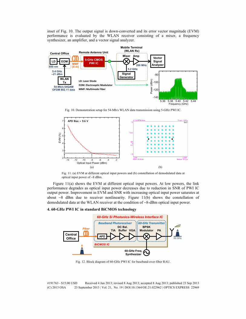
Fig. 9. Chip photo of 5-GHz PWI IC.
Figure 9 shows the chip photo of the 5-GHz PWI IC. The chip area including all probe pads is 0.9 mm × 1.8 mm. The IC consumes 155.7 mW from 1.8-V supply. The PA consumes most of the power.
Figure 10 shows the experimental setup used for RF-over-fiber demonstration. A vector signal generator provides 54-Mb/s WLAN data in 5 GHz. An 850-nm electrooptic modulator (EOM) modulates light from an 850-nm laser diode with the WLAN signals. Modulating electrical power is set to −21 dBm in order to minimize the EOM nonlinearity. The optical signal is injected through a lensed fiber into the PWI IC in an on-wafer probing setup. The PWI IC converts the optical signal into the wireless signal whose spectrum is shown in the
#191763 - $15.00 USD Received 4 Jun 2013; revised 8 Aug 2013; accepted 8 Aug 2013; published 23 Sep 2013(C) 2013 OSA 23 September 2013 | Vol. 21, No. 19 | DOI:10.1364/OE.21.022962 | OPTICS EXPRESS 22968
inset of Fig. 10. The output signal is down-converted and its error vector magnitude (EVM) performance is evaluated by the WLAN receiver consisting of a mixer, a frequency synthesizer, an amplifier, and a vector signal analyzer.
AmpMixer
Mobile Terminal (WLAN Rx)
5.2 GHz
SignalGenerator
VectorSignal
Analyzer
Remote Antenna Unit
5-GHz CMOSPWI IC
5.36 5.38 5.40 5.42 5.44
-140
-120
-100
-80
Frequency (GHz)
200 MHz
LD: Laser DiodeEOM: Electrooptic ModulatorMMF: Multimode Fiber
Po
wer
(dB
m)
Frequency (GHz)
5.4 GHz–21 dBm
54-Mb/s 64QAMOFDM 802.11 data
EOMLD
850 nm
Central Office
WLANTx
MMF(4 m)
Fig. 10. Demonstration setup for 54-Mb/s WLAN data transmission using 5-GHz PWI IC.
(b)
-14 -12 -10 -8 -6 -4 -22
3
4
5
6
7
EV
M (
%)
Optical Input Power (dBm)
APD bias = 9.6 V
(a)
APD Bias = 9.6 V
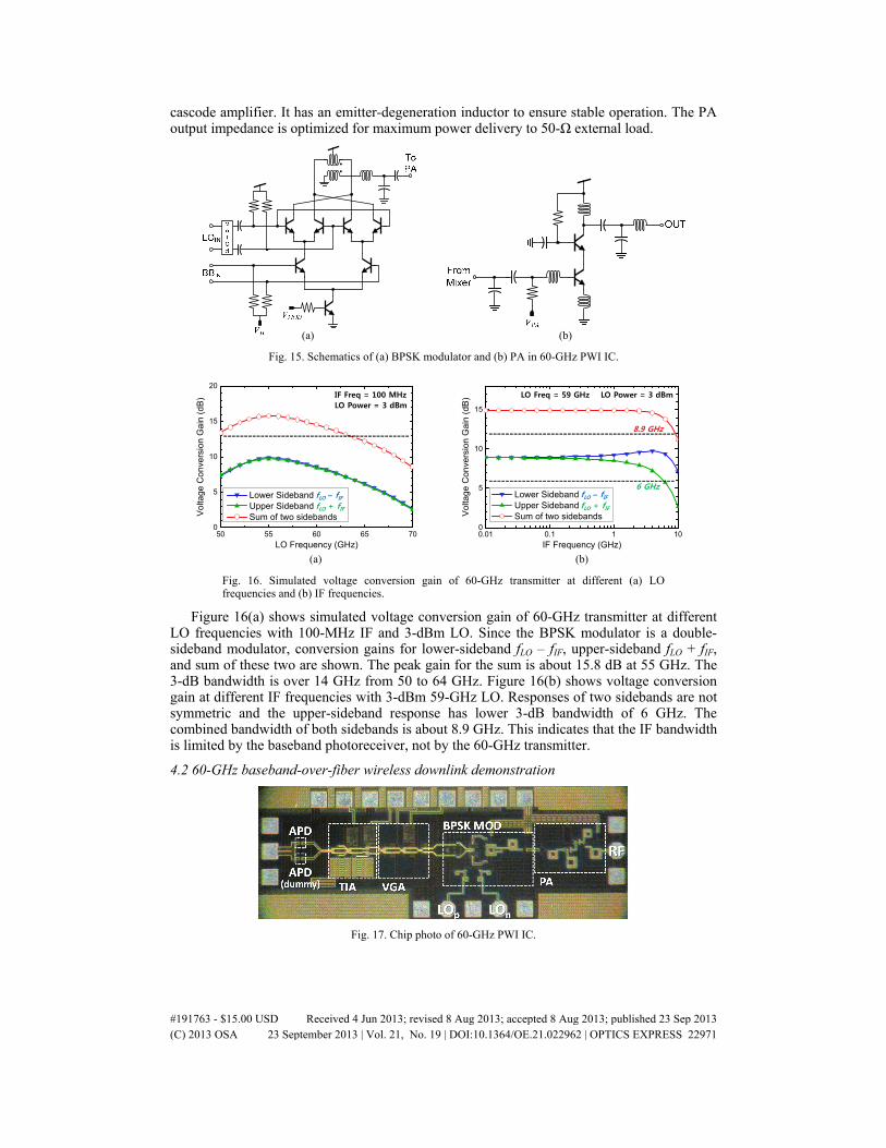
Fig. 11. (a) EVM at different optical input powers and (b) constellation of demodulated data at optical input power of −8 dBm.
Figure 11(a) shows the EVM at different optical input powers. At low powers, the link performance degrades as optical input power decreases due to reduction in SNR of PWI IC output power. Improvement in EVM and SNR with increasing optical input power saturates at about −8 dBm due to receiver nonlinearity. Figure 11(b) shows the constellation of demodulated data at the WLAN receiver at the condition of −8-dBm optical input power.
4. 60-GHz PWI IC in standard BiCMOS technology
Baseband Photoreceiver
VGATIA
60 GHz
60-GHz Si Photonics-Wireless Interface IC
APD
Fiber
CentralOffice
BiCMOS IC
PABPSK
Modulator
60-GHz Freq.Synthesizer
DC Bal.Buffer
60-GHz Transmitter
Fig. 12. Block diagram of 60-GHz PWI IC for baseband-over-fiber RAU.
#191763 - $15.00 USD Received 4 Jun 2013; revised 8 Aug 2013; accepted 8 Aug 2013; published 23 Sep 2013(C) 2013 OSA 23 September 2013 | Vol. 21, No. 19 | DOI:10.1364/OE.21.022962 | OPTICS EXPRESS 22969
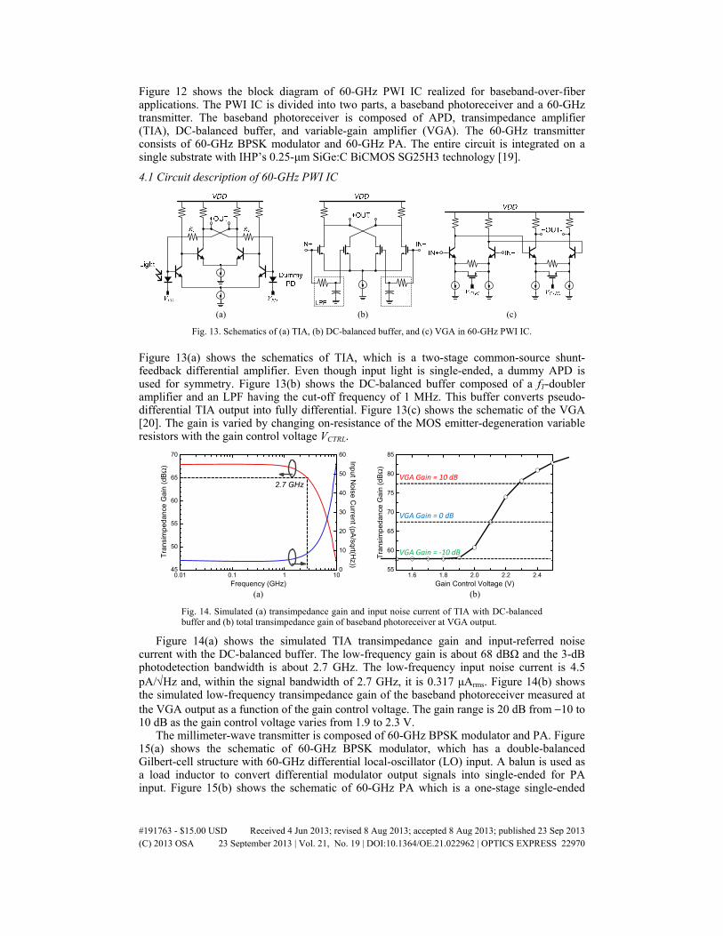
Figure 12 shows the block diagram of 60-GHz PWI IC realized for baseband-over-fiber applications. The PWI IC is divided into two parts, a baseband photoreceiver and a 60-GHz transmitter. The baseband photoreceiver is composed of APD, transimpedance amplifier (TIA), DC-balanced buffer, and variable-gain amplifier (VGA). The 60-GHz transmitter consists of 60-GHz BPSK modulator and 60-GHz PA. The entire circuit is integrated on a single substrate with IHP’s 0.25-μm SiGe:C BiCMOS SG25H3 technology [19].
4.1 Circuit description of 60-GHz PWI IC
(b)(a) (c)
Fig. 13. Schematics of (a) TIA, (b) DC-balanced buffer, and (c) VGA in 60-GHz PWI IC.
Figure 13(a) shows the schematics of TIA, which is a two-stage common-source shunt-feedback differential amplifier. Even though input light is single-ended, a dummy APD is used for symmetry. Figure 13(b) shows the DC-balanced buffer composed of a fT-doubler amplifier and an LPF having the cut-off frequency of 1 MHz. This buffer converts pseudo-differential TIA output into fully differential. Figure 13(c) shows the schematic of the VGA [20]. The gain is varied by changing on-resistance of the MOS emitter-degeneration variable resistors with the gain control voltage VCTRL.
(b)(a)
0.01 0.1 1 1045
50
55
60
65
70
Tra
nsi
mp
eda
nce
Ga
in (
dB
Ω)
Frequency (GHz)
0
10
20
30
40
50
60
Inp
ut N
oise C
urre
nt (pA
/sqrt(H
z))
1.6 1.8 2.0 2.2 2.455
60
65
70
75
80
85
Tra
nsi
mp
ed
an
ce G
ain
(d
BΩ
)
Gain Control Voltage (V)
VGA Gain = -10 dB
VGA Gain = 0 dB
VGA Gain = 10 dB2.7 GHz
Fig. 14. Simulated (a) transimpedance gain and input noise current of TIA with DC-balanced buffer and (b) total transimpedance gain of baseband photoreceiver at VGA output.
Figure 14(a) shows the simulated TIA transimpedance gain and input-referred noise current with the DC-balanced buffer. The low-frequency gain is about 68 dBΩ and the 3-dB photodetection bandwidth is about 2.7 GHz. The low-frequency input noise current is 4.5 pA/√Hz and, within the signal bandwidth of 2.7 GHz, it is 0.317 μArms. Figure 14(b) shows the simulated low-frequency transimpedance gain of the baseband photoreceiver measured at the VGA output as a function of the gain control voltage. The gain range is 20 dB from −10 to 10 dB as the gain control voltage varies from 1.9 to 2.3 V.
The millimeter-wave transmitter is composed of 60-GHz BPSK modulator and PA. Figure 15(a) shows the schematic of 60-GHz BPSK modulator, which has a double-balanced Gilbert-cell structure with 60-GHz differential local-oscillator (LO) input. A balun is used as a load inductor to convert differential modulator output signals into single-ended for PA input. Figure 15(b) shows the schematic of 60-GHz PA which is a one-stage single-ended
#191763 - $15.00 USD Received 4 Jun 2013; revised 8 Aug 2013; accepted 8 Aug 2013; published 23 Sep 2013(C) 2013 OSA 23 September 2013 | Vol. 21, No. 19 | DOI:10.1364/OE.21.022962 | OPTICS EXPRESS 22970
cascode amplifier. It has an emitter-degeneration inductor to ensure stable operation. The PA output impedance is optimized for maximum power delivery to 50-Ω external load.
(b)(a)
Fig. 15. Schematics of (a) BPSK modulator and (b) PA in 60-GHz PWI IC.
(b)(a)
50 55 60 65 700
5
10
15
20
Vol
tage
Con
vers
ion
Gai
n (
dB)
LO Frequency (GHz)
Lower Sideband Upper Sideband Sum of two sidebands
fLO – fIFfLO + fIF
IF Freq = 100 MHzLO Power = 3 dBm
0.01 0.1 1 100
5
10
15
Vol
tage
Con
vers
ion
Gai
n (d
B)
IF Frequency (GHz)
Lower Sideband Upper Sideband Sum of two sidebands
8.9 GHz
6 GHz
LO Freq = 59 GHz LO Power = 3 dBm
fLO – fIFfLO + fIF
Fig. 16. Simulated voltage conversion gain of 60-GHz transmitter at different (a) LO frequencies and (b) IF frequencies.
Figure 16(a) shows simulated voltage conversion gain of 60-GHz transmitter at different LO frequencies with 100-MHz IF and 3-dBm LO. Since the BPSK modulator is a double-sideband modulator, conversion gains for lower-sideband fLO – fIF, upper-sideband fLO + fIF, and sum of these two are shown. The peak gain for the sum is about 15.8 dB at 55 GHz. The 3-dB bandwidth is over 14 GHz from 50 to 64 GHz. Figure 16(b) shows voltage conversion gain at different IF frequencies with 3-dBm 59-GHz LO. Responses of two sidebands are not symmetric and the upper-sideband response has lower 3-dB bandwidth of 6 GHz. The combined bandwidth of both sidebands is about 8.9 GHz. This indicates that the IF bandwidth is limited by the baseband photoreceiver, not by the 60-GHz transmitter.
4.2 60-GHz baseband-over-fiber wireless downlink demonstration
Fig. 17. Chip photo of 60-GHz PWI IC.
#191763 - $15.00 USD Received 4 Jun 2013; revised 8 Aug 2013; accepted 8 Aug 2013; published 23 Sep 2013(C) 2013 OSA 23 September 2013 | Vol. 21, No. 19 | DOI:10.1364/OE.21.022962 | OPTICS EXPRESS 22971
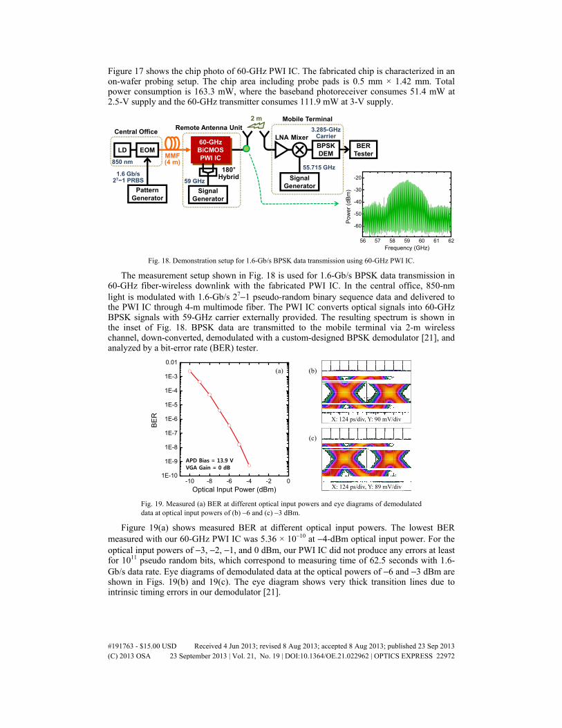
Figure 17 shows the chip photo of 60-GHz PWI IC. The fabricated chip is characterized in an on-wafer probing setup. The chip area including probe pads is 0.5 mm × 1.42 mm. Total power consumption is 163.3 mW, where the baseband photoreceiver consumes 51.4 mW at 2.5-V supply and the 60-GHz transmitter consumes 111.9 mW at 3-V supply.
LNA Mixer
Mobile Terminal2 m
55.715 GHz
3.285-GHzCarrier
EOMLD
850 nm
Central Office
1.6 Gb/s27−1 PRBS
PatternGenerator
SignalGenerator
BERTester
Remote Antenna Unit
59 GHz
60-GHz BiCMOSPWI IC
SignalGenerator
180°Hybrid
56 57 58 59 60 61 62
-60
-50
-40
-30
-20
Pow
er (
dBm
)
Frequency (GHz)
BPSKDEMMMF
(4 m)
Fig. 18. Demonstration setup for 1.6-Gb/s BPSK data transmission using 60-GHz PWI IC.
The measurement setup shown in Fig. 18 is used for 1.6-Gb/s BPSK data transmission in 60-GHz fiber-wireless downlink with the fabricated PWI IC. In the central office, 850-nm light is modulated with 1.6-Gb/s 27−1 pseudo-random binary sequence data and delivered to the PWI IC through 4-m multimode fiber. The PWI IC converts optical signals into 60-GHz BPSK signals with 59-GHz carrier externally provided. The resulting spectrum is shown in the inset of Fig. 18. BPSK data are transmitted to the mobile terminal via 2-m wireless channel, down-converted, demodulated with a custom-designed BPSK demodulator [21], and analyzed by a bit-error rate (BER) tester.
-10 -8 -6 -4 -2 01E-10
1E-9
1E-8
1E-7
1E-6
1E-5
1E-4
1E-3
0.01
BE
R
Optical Input Power (dBm)
(b)(a)
X: 124 ps/div, Y: 90 mV/div
X: 124 ps/div, Y: 89 mV/div
(c)
APD Bias = 13.9 VVGA Gain = 0 dB
Fig. 19. Measured (a) BER at different optical input powers and eye diagrams of demodulated data at optical input powers of (b) −6 and (c) −3 dBm.
Figure 19(a) shows measured BER at different optical input powers. The lowest BER measured with our 60-GHz PWI IC was 5.36 × 10⁻¹⁰ at −4-dBm optical input power. For the optical input powers of −3, −2, −1, and 0 dBm, our PWI IC did not produce any errors at least for 1011 pseudo random bits, which correspond to measuring time of 62.5 seconds with 1.6-Gb/s data rate. Eye diagrams of demodulated data at the optical powers of −6 and −3 dBm are shown in Figs. 19(b) and 19(c). The eye diagram shows very thick transition lines due to intrinsic timing errors in our demodulator [21].
#191763 - $15.00 USD Received 4 Jun 2013; revised 8 Aug 2013; accepted 8 Aug 2013; published 23 Sep 2013(C) 2013 OSA 23 September 2013 | Vol. 21, No. 19 | DOI:10.1364/OE.21.022962 | OPTICS EXPRESS 22972

5. Conclusion
A 5-GHz RF-over-fiber PWI IC and a 60-GHz baseband-over-fiber PWI IC are successfully realized in standard Si technology. The performance of each PWI IC is verified with data transmission in fiber-wireless downlink. Although these PWI ICs have limited functionalities to be used in applications, they demonstrate the feasibility of applying Si EPIC technology for realizing cost-effective and compact RAUs in future fiber-wireless networks.
Acknowledgments
This work was supported by the National Research Foundation of Korea funded by the Korean Government (MEST) under Grant 2012R1A2A1A01009233. The authors would like to thank IC Design Education Center (IDEC) for EDA software support.
#191763 - $15.00 USD Received 4 Jun 2013; revised 8 Aug 2013; accepted 8 Aug 2013; published 23 Sep 2013(C) 2013 OSA 23 September 2013 | Vol. 21, No. 19 | DOI:10.1364/OE.21.022962 | OPTICS EXPRESS 22973