Embed Size (px)
DESCRIPTION
athena summary
Citation preview

EEE 533 Semiconductor Device and Process Simulation
Introduction to Silvaco ATHENA Tool and
Basic Concepts in Process Modeling
Part - 3
Instructor: Dragica Vasileska
Department of Electrical Engineering
Arizona State University
EEE 533 Semiconductor Device and Process Simulation
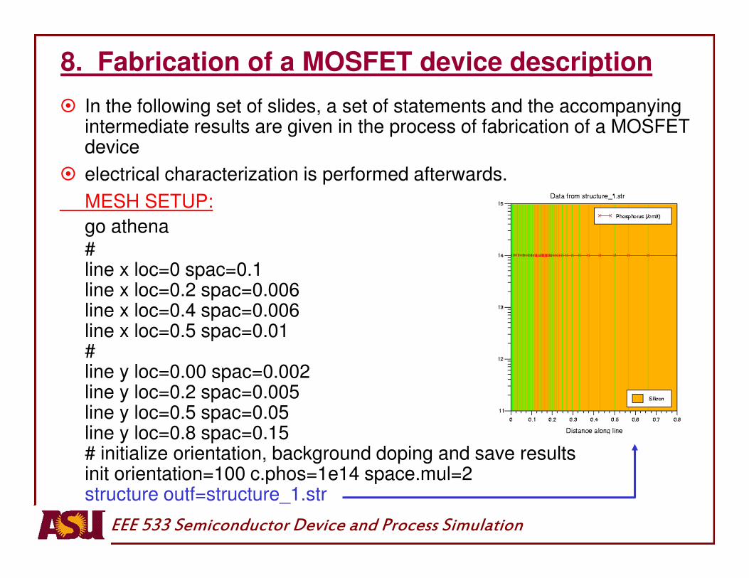
8. Fabrication of a MOSFET device description
� In the following set of slides, a set of statements and the accompanying intermediate results are given in the process of fabrication of a MOSFET device
� electrical characterization is performed afterwards.
MESH SETUP:
go athena#line x loc=0 spac=0.1 line x loc=0.2 spac=0.006line x loc=0.4 spac=0.006line x loc=0.5 spac=0.01 #line y loc=0.00 spac=0.002 line y loc=0.2 spac=0.005line y loc=0.5 spac=0.05line y loc=0.8 spac=0.15 # initialize orientation, background doping and save resultsinit orientation=100 c.phos=1e14 space.mul=2structure outf=structure_1.str
EEE 533 Semiconductor Device and Process Simulation
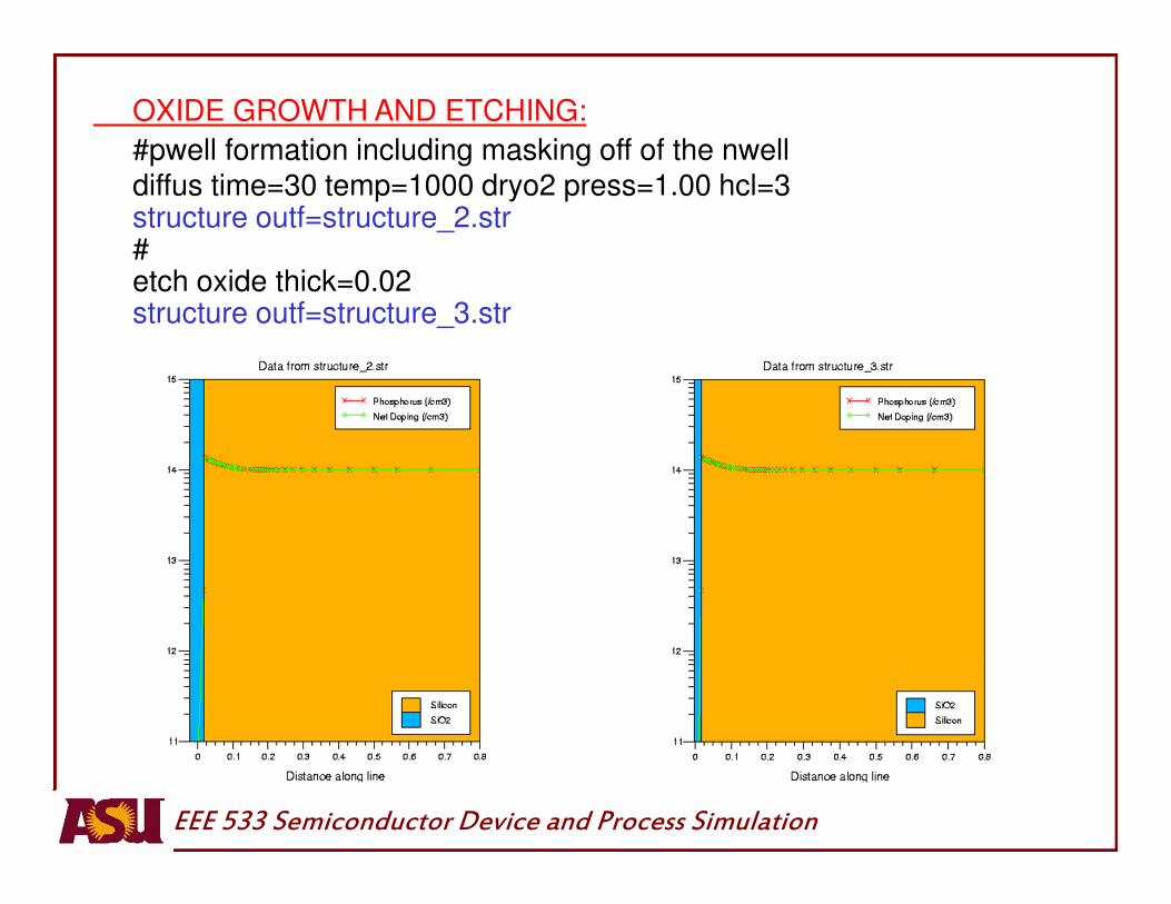
OXIDE GROWTH AND ETCHING:
#pwell formation including masking off of the nwelldiffus time=30 temp=1000 dryo2 press=1.00 hcl=3structure outf=structure_2.str#etch oxide thick=0.02structure outf=structure_3.str

EEE 533 Semiconductor Device and Process Simulation
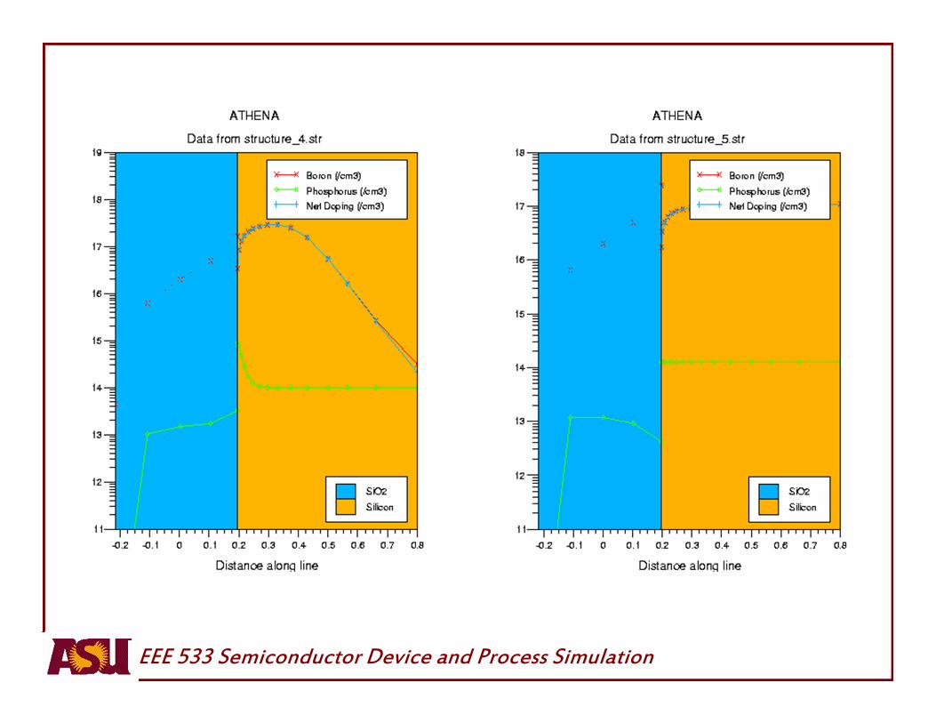
P-WELL FORMATION AND OXIDE GROWTH AND ETCHING:
# P-well Implantimplant boron dose=8e12 energy=100 pears diffus temp=950 time=100 weto2 hcl=3structure outf=structure_4.str## N-well implant not shown -## welldrive starts herediffus time=50 temp=1000 t.rate=4.000 dryo2 press=0.10 hcl=3diffus time=220 temp=1200 nitro press=1diffus time=90 temp=1200 t.rate=-4.444 nitro press=1structure outf=structure_5.str#etch oxide all## sacrificial "cleaning" oxidediffus time=20 temp=1000 dryo2 press=1 hcl=3#etch oxide all#
EEE 533 Semiconductor Device and Process Simulation
EEE 533 Semiconductor Device and Process Simulation
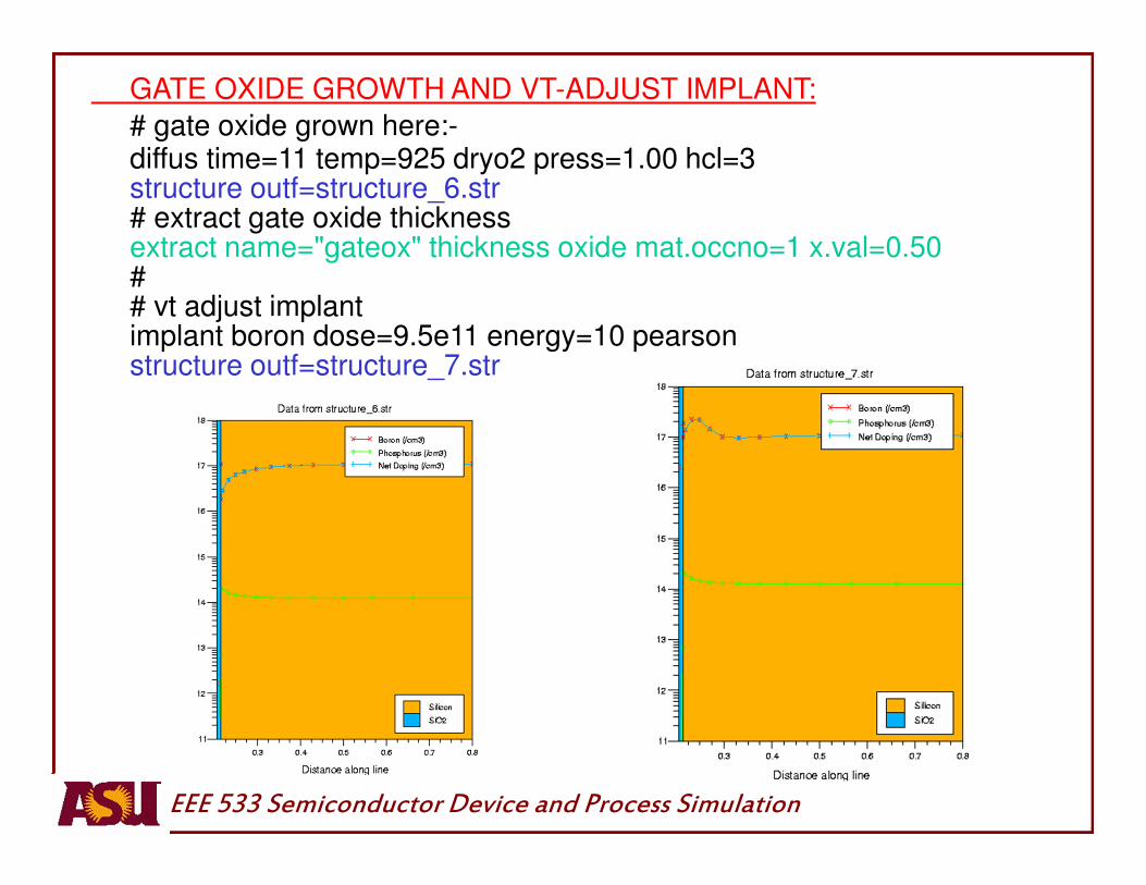
GATE OXIDE GROWTH AND VT-ADJUST IMPLANT:
# gate oxide grown here:-diffus time=11 temp=925 dryo2 press=1.00 hcl=3structure outf=structure_6.str# extract gate oxide thicknessextract name="gateox" thickness oxide mat.occno=1 x.val=0.50## vt adjust implant implant boron dose=9.5e11 energy=10 pearsonstructure outf=structure_7.str

EEE 533 Semiconductor Device and Process Simulation
POLYSILICON DEPOSITION AND ETCHING:
# Polysilicon depositiondepo poly thick=0.2 divi=10 structure outf=structure_8.str## from now on the situation is 2-D#etch poly left p1.x=0.35structure outf=structure_9.str
EEE 533 Semiconductor Device and Process Simulation
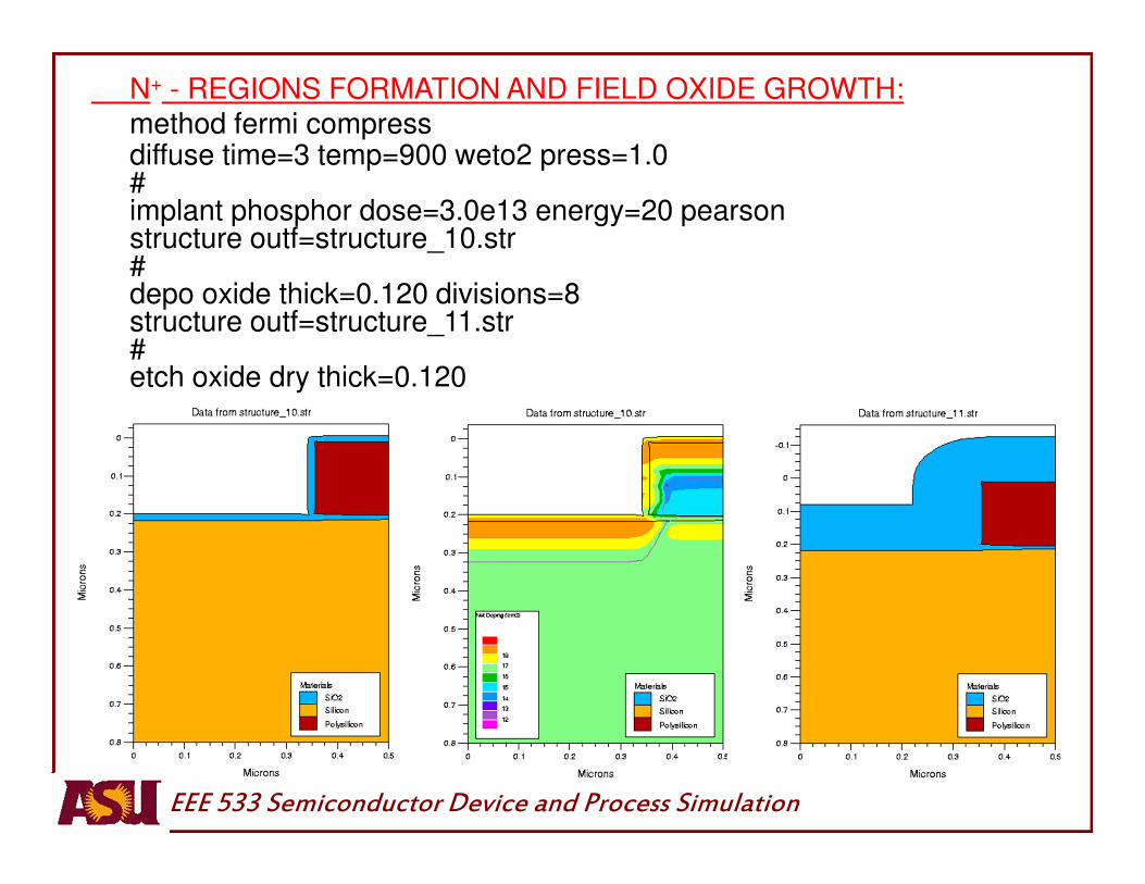
N+ - REGIONS FORMATION AND FIELD OXIDE GROWTH:method fermi compressdiffuse time=3 temp=900 weto2 press=1.0#implant phosphor dose=3.0e13 energy=20 pearsonstructure outf=structure_10.str #depo oxide thick=0.120 divisions=8structure outf=structure_11.str#etch oxide dry thick=0.120

EEE 533 Semiconductor Device and Process Simulation
ARSENIC IMPLANTATION AND OXIDE ETCHING:implant arsenic dose=5.0e15 energy=50 pearson #method fermi compressdiffuse time=1 temp=900 nitro press=1.0structure outf=structure_12.str#etch oxide left p1.x=0.2structure outf=structure_13.str
EEE 533 Semiconductor Device and Process Simulation
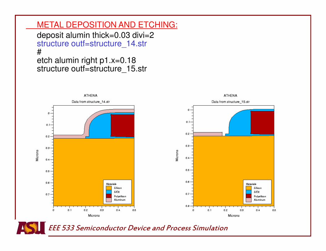
METAL DEPOSITION AND ETCHING:
deposit alumin thick=0.03 divi=2structure outf=structure_14.str#etch alumin right p1.x=0.18structure outf=structure_15.str

EEE 533 Semiconductor Device and Process Simulation
EXTRACTION OF DEVICE DESIGN PARAMETERS:
# extract final S/D Xj...extract name="nxj" xj silicon mat.occno=1 x.val=0.1 junc.occno=1
# extract the long chan Vt...extract name="n1dvt" 1dvt ntype vb=0.0 qss=1e10 x.val=0.49
# extract a curve of conductance versus bias....extract start material="Polysilicon" mat.occno=1 \
bias=0.0 bias.step=0.2 bias.stop=2 x.val=0.45extract done name="sheet cond v bias" curve(bias,1dn.conduct \
material="Silicon" mat.occno=1 region.occno=1) outfile="extract.dat”
# extract the N++ regions sheet resistance...extract name="n++ sheet rho" sheet.res material="Silicon" mat.occno=1 \
x.val=0.05 region.occno=1
# extract the sheet rho under the spacer, of the LDD region...extract name="ldd sheet rho" sheet.res material="Silicon" mat.occno=1 \
x.val=0.3 region.occno=1
# extract the surface conc under the channel....extract name="chan surf conc" surf.conc impurity="Net Doping" \
material="Silicon" mat.occno=1 x.val=0.45
EEE 533 Semiconductor Device and Process Simulation
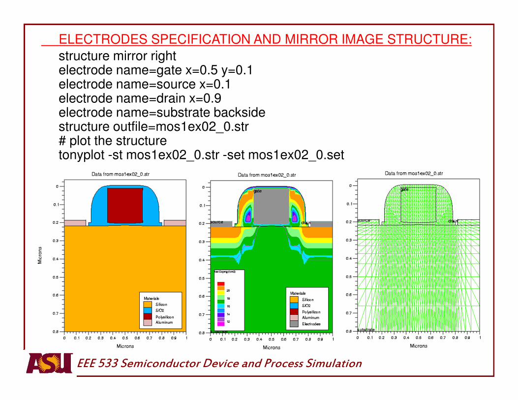
ELECTRODES SPECIFICATION AND MIRROR IMAGE STRUCTURE:
structure mirror rightelectrode name=gate x=0.5 y=0.1electrode name=source x=0.1electrode name=drain x=0.9electrode name=substrate backsidestructure outfile=mos1ex02_0.str# plot the structuretonyplot -st mos1ex02_0.str -set mos1ex02_0.set
EEE 533 Semiconductor Device and Process Simulation
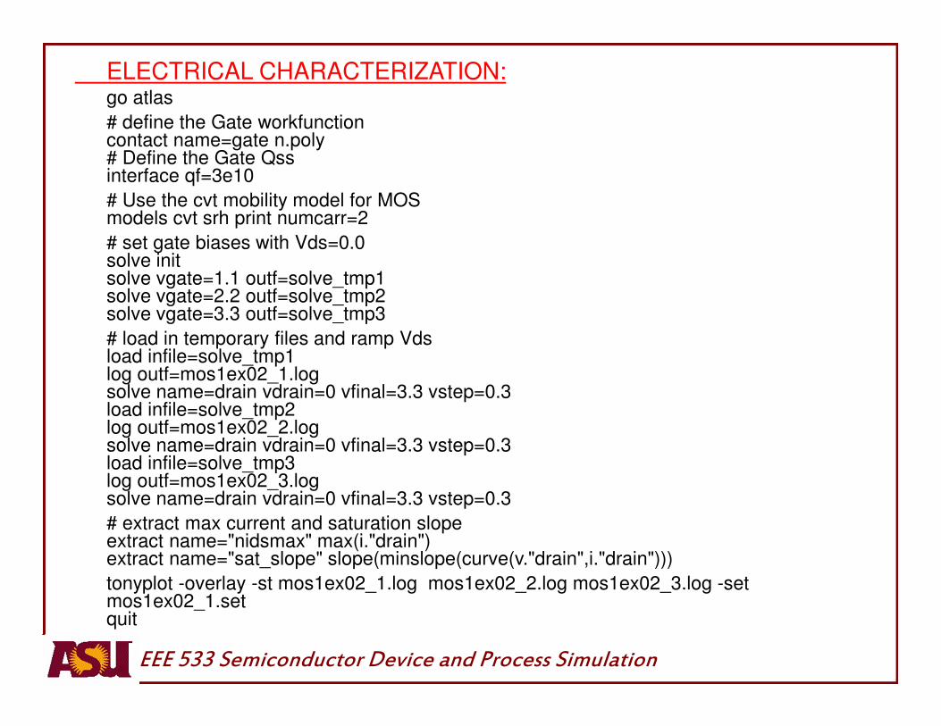
ELECTRICAL CHARACTERIZATION:go atlas
# define the Gate workfunction contact name=gate n.poly# Define the Gate Qssinterface qf=3e10
# Use the cvt mobility model for MOS models cvt srh print numcarr=2
# set gate biases with Vds=0.0 solve initsolve vgate=1.1 outf=solve_tmp1 solve vgate=2.2 outf=solve_tmp2 solve vgate=3.3 outf=solve_tmp3
# load in temporary files and ramp Vdsload infile=solve_tmp1log outf=mos1ex02_1.logsolve name=drain vdrain=0 vfinal=3.3 vstep=0.3 load infile=solve_tmp2log outf=mos1ex02_2.logsolve name=drain vdrain=0 vfinal=3.3 vstep=0.3 load infile=solve_tmp3log outf=mos1ex02_3.logsolve name=drain vdrain=0 vfinal=3.3 vstep=0.3
# extract max current and saturation slope extract name="nidsmax" max(i."drain")extract name="sat_slope" slope(minslope(curve(v."drain",i."drain")))
tonyplot -overlay -st mos1ex02_1.log mos1ex02_2.log mos1ex02_3.log -set mos1ex02_1.setquit

EEE 533 Semiconductor Device and Process Simulation
OBTAINED SIMULATION RESULTS:
Content of the results.final file:
gateox=100.164 angstroms (0.0100164 um) X.val=0.5
nxj=0.174465 um from top of first Silicon layer X.val=0.1
n1dvt=0.59203 V X.val=0.49
n++ sheet rho=29.0223 ohm/square X.val=0.05
ldd sheet rho=2149.79 ohm/square X.val=0.3
chan surf conc=3.90871e+16 atoms/cm3 X.val=0.45
nidsmax=0.000563816
sat_slope=1.94223e-05

EEE 533 Semiconductor Device and Process Simulation
9. Additional Silvaco ATHENA examples
go athena
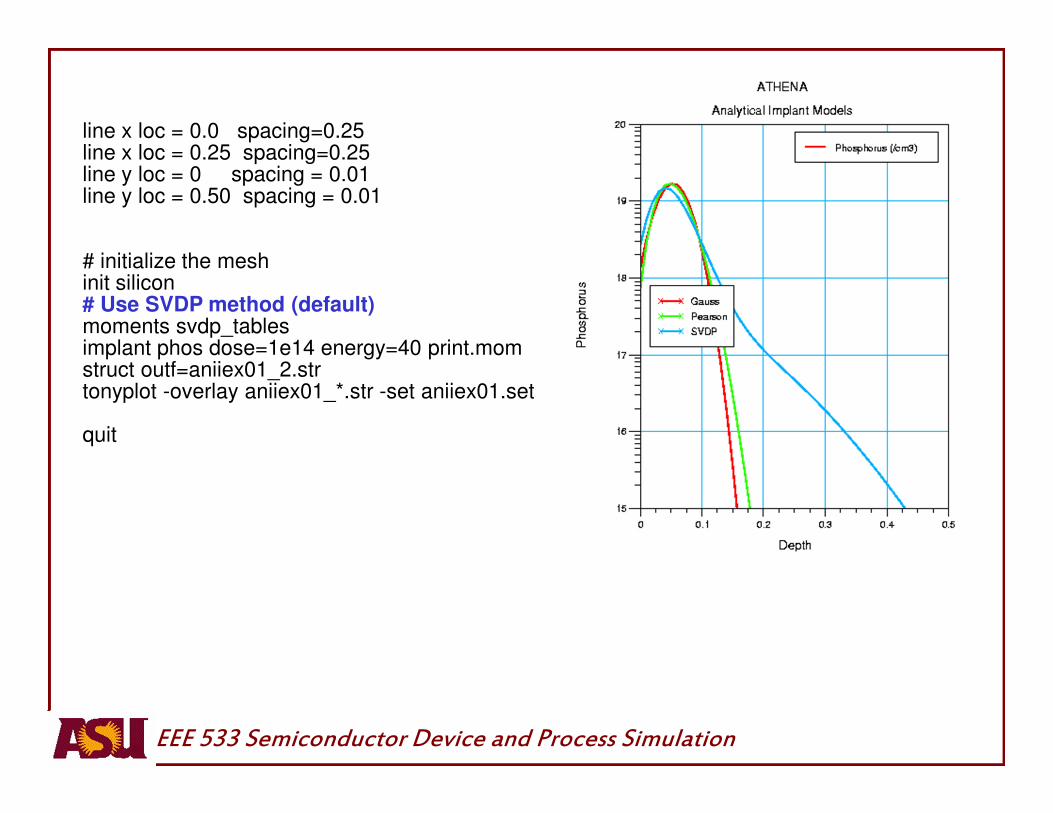
# TITLE: Comparison of Gauss, Pearson and SVDP method
line x loc = 0.0 spacing=0.25line x loc = 0.25 spacing=0.25line y loc = 0 spacing = 0.01 line y loc = 0.50 spacing = 0.01
#initialize the meshinit silicon # Gauss (symmetrical) implant (parameters are in std_tables)moments std_tablesimplant phos dose=1e14 energy=40 gauss struct outf=aniiex01_0.str
line x loc = 0.0 spacing=0.25line x loc = 0.25 spacing=0.25line y loc = 0 spacing = 0.01 line y loc = 0.50 spacing = 0.01
# initialize the meshinit silicon # Use single Pearson (parameters are in std_tables)moments std_tablesimplant phos dose=1e14 energy=40 pearson print.momstruct outf=aniiex01_1.str
EEE 533 Semiconductor Device and Process Simulation
line x loc = 0.0 spacing=0.25line x loc = 0.25 spacing=0.25line y loc = 0 spacing = 0.01 line y loc = 0.50 spacing = 0.01
# initialize the meshinit silicon # Use SVDP method (default)moments svdp_tables implant phos dose=1e14 energy=40 print.momstruct outf=aniiex01_2.strtonyplot -overlay aniiex01_*.str -set aniiex01.set
quit
EEE 533 Semiconductor Device and Process Simulation
go athena
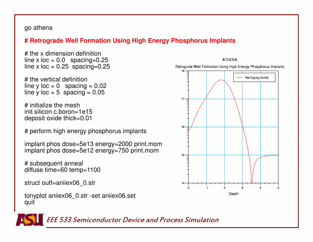
# Retrograde Well Formation Using High Energy Phosphorus Implants
# the x dimension definitionline x loc = 0.0 spacing=0.25line x loc = 0.25 spacing=0.25
# the vertical definitionline y loc = 0 spacing = 0.02 line y loc = 5 spacing = 0.05
# initialize the meshinit silicon c.boron=1e15deposit oxide thick=0.01
# perform high energy phosphorus implants
implant phos dose=5e13 energy=2000 print.momimplant phos dose=5e12 energy=750 print.mom
# subsequent annealdiffuse time=60 temp=1100
struct outf=aniiex06_0.str
tonyplot aniiex06_0.str -set aniiex06.setquit
EEE 533 Semiconductor Device and Process Simulation
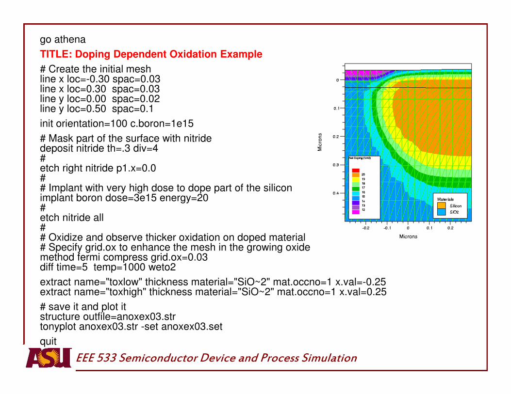
go athena
TITLE: Doping Dependent Oxidation Example
# Create the initial meshline x loc=-0.30 spac=0.03line x loc=0.30 spac=0.03line y loc=0.00 spac=0.02line y loc=0.50 spac=0.1
init orientation=100 c.boron=1e15
# Mask part of the surface with nitridedeposit nitride th=.3 div=4#etch right nitride p1.x=0.0## Implant with very high dose to dope part of the siliconimplant boron dose=3e15 energy=20#etch nitride all## Oxidize and observe thicker oxidation on doped material# Specify grid.ox to enhance the mesh in the growing oxide method fermi compress grid.ox=0.03diff time=5 temp=1000 weto2
extract name="toxlow" thickness material="SiO~2" mat.occno=1 x.val=-0.25extract name="toxhigh" thickness material="SiO~2" mat.occno=1 x.val=0.25
# save it and plot itstructure outfile=anoxex03.str tonyplot anoxex03.str -set anoxex03.set
quit

EEE 533 Semiconductor Device and Process Simulation
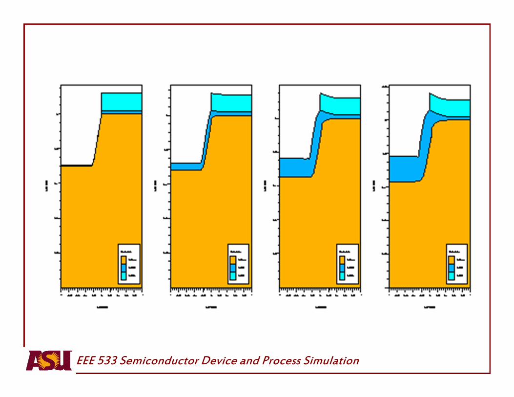
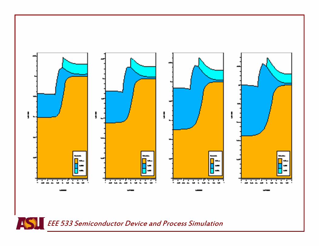
go athena
# TITLE: Oxide Profile Evolution Example
# Substrate mesh definitionline y loc=0 spac=0.05line y loc=0.6 spac=0.2line y loc=1 line x loc=-1 spac=0.2line x loc=-0.2 spac=0.05line x loc=0 spac=0.05line x loc=1 spac=0.2
init orient=100
# Anisotropic silicon etchetch silicon left p1.x=-0.218 p1.y=0.3 p2.x=0 p2.y=0
# Pad oxide and nitride maskdeposit oxide thick=0.02deposit nitride thick=0.1
etch nitride left p1.x=0etch oxide left p1.x=0
# Field oxidation with structure file output for moviediffuse tim=90 tem=1000 weto2 dump=1 dump.prefix=anoxex01m
tonyplot -st anoxex01m*.str structure outfile=anoxex01_0.str
quit
EEE 533 Semiconductor Device and Process Simulation
EEE 533 Semiconductor Device and Process Simulation


![ATHENA - Coordinate System Document...[RD02] ATHENA Mission Requirements Document (MRD), ATHENA-ESA-URD-0010 [RD03] ATHENA Product Tree, ATHENA-ESA-PT-0001 [RD04] Ariane 5 User’s](https://img.pdfslide.net/doc/110x75/5ff23cd84225de2c7f4f21b6/athena-coordinate-system-document-rd02-athena-mission-requirements-document.jpg)