Embed Size (px)
Citation preview

Lab Workbook Simple Hardware Design Using AXI
www.xilinx.com/university Nexys3 1-1 [email protected] © Copyright 2012 Xilinx
Simple Hardware Design Using AXI
Introduction
This lab guides you through the process of using Xilinx Platform Studio (XPS) to create a simple MicroBlaze based processor system using AXI4 interface and targeting the Nexys3 Board
Objectives
After completing this lab, you will be able to:
• Create an XPS project by using the Base System Builder (BSB)
• Create a simple hardware design by using Xilinx AXI4 interface based IP cores available in the Embedded Development Kit
Procedure
This lab is separated into steps that consist of general overview statements that provide information on the detailed instructions that follow. Follow these detailed instructions to progress through the lab.
This lab comprises 5 primary steps: You will create a project using the Base System Builder, analyze the created project, generate netlist and hardware bitstream, create a Memory TestApp in SDK, and, finally, test in hardware.
Design Description
The purpose of the lab exercises is to walk you through a complete hardware and software processor system design. Each lab will build upon the previous lab. The following diagram represents the completed design (Figure 1).
Figure 1. Completed Design
In this lab, you will use the BSB of the XPS system to create a processor system consisting of the following processor IP (Figure 2):
• MicroBlaze (version 8.40.a)

Simple Hardware Design Using AXI Lab Workbook
Nexys3 1-2 www.xilinx.com/university [email protected] © Copyright 2012 Xilinx
• AXI4 Interconnect Blocks
• LMB BRAM controllers for BRAM
• BRAM • UART for serial communication
Figure 2. Processor Design of this Lab
General Flow for this Lab
Step 1: Create a
project using the Base System Builder
Step 2: Analyze the
created project
Step 3: Generate Netlist and Bitstream
Step 4:
Create a Memory
TestApp in SDK
Step 5:
Test in hardware

Lab Workbook Simple Hardware Design Using AXI
www.xilinx.com/university Nexys3 1-3 [email protected] © Copyright 2012 Xilinx
Creating the Project Using the Base System Builder Step 1
1-1. Launch Xilinx Platform Studio (XPS) and create a new project. Use Base System Builder to generate a MicroBlaze processor based hardware system using AXI system, targeting the Nexys3 Board.
1-1-1. Open XPS by selecting Start > All Programs > Xilinx Design Tools > ISE Design Suite 14.2 > EDK > Xilinx Platform Studio.
1-1-2. Click Create New Project Using Base System Builder to start the wizard. You can select File > New BSB Project and the same dialog box will appear.
Figure 3. New Project Creation Using Base System Builder
1-1-3. Browse to c:\xup\embedded\labs directory, create a new folder called lab1, select it, and click Open followed by click Save. Click OK.
1-1-4. Make sure to select the AXI system and click OK.
1-1-5. Click on the Browse… button of Set Project Peripheral Repository Search Path, navigate to c:\xup\embedded\sources\Nexys3_AXI_BSB_Support\lib, and click OK.

Simple Hardware Design Using AXI Lab Workbook
Nexys3 1-4 www.xilinx.com/university [email protected] © Copyright 2012 Xilinx
Figure 4. Assigning Project Directory
1-1-6. In the Board and System Selection dialog box, specify the settings below and click Next to continue.
o Board Vendor: Digilent
o Board Name: Digilent Nexys3 FPGA Board
o Board Revision (Verify on board): B
o Select a System : Single MicroBlaze Processor System
Lab Workbook Simple Hardware Design Using AXI
www.xilinx.com/university Nexys3 1-5 [email protected] © Copyright 2012 Xilinx
Figure 5. Board and System Selection Dialog Box
Note: if there’s no Nexys3 in your list. Please uninstall the Nexys3 board package. Refer to the readme_Nexys3board.txt file available at http://www.xilinx.com/university/workshops/embedded-system-design-flow/materials/14x/Nexys3-axi4/readme_Nexys3board.docx.
1-1-7. In the Processor, Cache, and Peripheral Configuration dialog box, set the value of Processor Frequency and Local Memory as 100 MHz and 16 KB respectively.
1-1-8. In the Included Peripherals for microblaze_0 field, click on Select All and then using Ctrl-key deselect RS232_Uart_1.
1-1-9. Click on <Remove button to remove the selected devices, leaving RS232_Uart_1 as the only external device to be used.
1-1-10. Configure RS232_Uart_1 with 115200 baud rate.

Simple Hardware Design Using AXI Lab Workbook
Nexys3 1-6 www.xilinx.com/university [email protected] © Copyright 2012 Xilinx
Figure 6. Processor, Cache, and Peripheral Configuration Dialog Box
You could use Add to add additional IO peripherals and internal peripherals, but you will see an alternative method in the next lab for adding internal peripherals to an existing project.
1-1-11. Click Finish.
1-1-12. A System Assembly View will be displayed showing peripherals and busses in the system, and the system connectivity.

Lab Workbook Simple Hardware Design Using AXI
www.xilinx.com/university Nexys3 1-7 [email protected] © Copyright 2012 Xilinx
Figure 7. System Assembly View
Analyze the Hardware Step 2
2-1. Select the Graphical Design View tab and study the system components and interconnections. Look in the System Assembly View and analyze the interface and port connections.
2-1-1. Click the Graphical Design View tab. You can use Ctrl key and mouse scroll to zoom in and out
the view. You can also use to change the colors of the objects in the view. Observe the various components that are used in the design

Simple Hardware Design Using AXI Lab Workbook
Nexys3 1-8 www.xilinx.com/university [email protected] © Copyright 2012 Xilinx
Figure 8. Block Diagram View of the Generated Project
You will see the MicroBlaze processor, one AXI Interconnects block- for AXI4-Lite capable devices. You will also see that the MDM and LMB are connected to the MicroBlaze ports directly.
2-1-2. In the System Assembly View click on plus button and observe the expanded (detailed) bus connection view of the system.

Lab Workbook Simple Hardware Design Using AXI
www.xilinx.com/university Nexys3 1-9 [email protected] © Copyright 2012 Xilinx
Figure 9. Detailed Bus Connections
Question 1
List the interface (bus name) instances to the following peripheral instances: debug_module: RS232_Uart_1:
2-1-3. Click on the Ports tab and have an expanded view. This is where you can make internal and external net connections. If you can’t find Net column then right click on the Connected Port on the ribbon to see available options and choose Net to get displayed.

Simple Hardware Design Using AXI Lab Workbook
Nexys3 1-10 www.xilinx.com/university [email protected] © Copyright 2012 Xilinx
Figure 10. Ports Filter
Question 2
List the nets which are connected to the following ports:
RS232_Uart_1 – (IO_IF) uart_0 – RX: RS232_Uart_1 – (IO_IF) uart_0 – TX:
2-1-4. Click on the Addresses tab. This is where you can assign or change base/high addresses of the peripherals in the system.
Figure 11. Assigned Base/High Addresses
Question 3
Select Addresses filter and list the address for the following instances:
RS232_Uart_1 – Base address: RS232_Uart_1– High address: microblaze_0_d_bram_ctrl – Base address: microblaze_0_d_bram_ctrl – High address: microblaze_0_i_bram_ctrl – Base address: microblaze_0_i_bram_ctrl – High address:
Lab Workbook Simple Hardware Design Using AXI
www.xilinx.com/university Nexys3 1-11 [email protected] © Copyright 2012 Xilinx
Generate Netlist and Bitstream Step 3
3-1. Run Platgen to generate the netlist and run implementation tools to generate the hardware bitstream.
3-1-1. Run PlatGen by selecting Hardware > Generate Netlist or click in the toolbar. You can also find Generate Netlist in the Implement Flow section of the Navigator window.
It will generate implementation, hdl, and synthesis directories. The generated peripherals and system netlists along with system.bmm will be placed in the implementation directory.
3-1-2. Run implementation tools (xflow) by selecting Hardware > Generate BitStream or click in the toolbar. You can also find Generate BitStream in the Implement Flow section of the Navigator window
It will take more than ten minutes (depends on your computer).
3-1-3. Click on the Design Summary tab. The Design Summary allows you to quickly access design overview information, reports, and messages. It displays information specific to your targeted device and software tools. The pane on the left side of the Design Summary allows you to control the information displayed in the right pane.
3-1-4. Browse to the Lab1 project directory using Windows Explorer.
Several directories containing VHDL wrappers and implementation netlists have been created.
Question 4
List the directories that were created.
____________________________________________________________________________________ ____________________________________________________________________________________
Generate Memory TestApp in SDK Step 4
4-1. Start SDK from XPS, generate memory test project with default software platform project.
4-1-1. Start SDK by clicking Project > Export Hardware Design to SDK … from XPS.
4-1-2. Click on Export & Launch SDK button with default settings (Include bitstream and BMM file checked).
4-1-3. In Select a workspace window, browse to c:\xup\embedded\labs\lab1\SDK\SDK_Export and click OK.

Simple Hardware Design Using AXI Lab Workbook
Nexys3 1-12 www.xilinx.com/university [email protected] © Copyright 2012 Xilinx
4-1-4. In SDK, select File > New > Xilinx C Project, select Memory Tests from the Select Project Template window, and then click Next.
Figure 12. Creating Memory Tests C Project
4-1-5. Click Finish with default settings (with memory_tests_bsp_0 as the default Board Support Package).
Lab Workbook Simple Hardware Design Using AXI
www.xilinx.com/university Nexys3 1-13 [email protected] © Copyright 2012 Xilinx
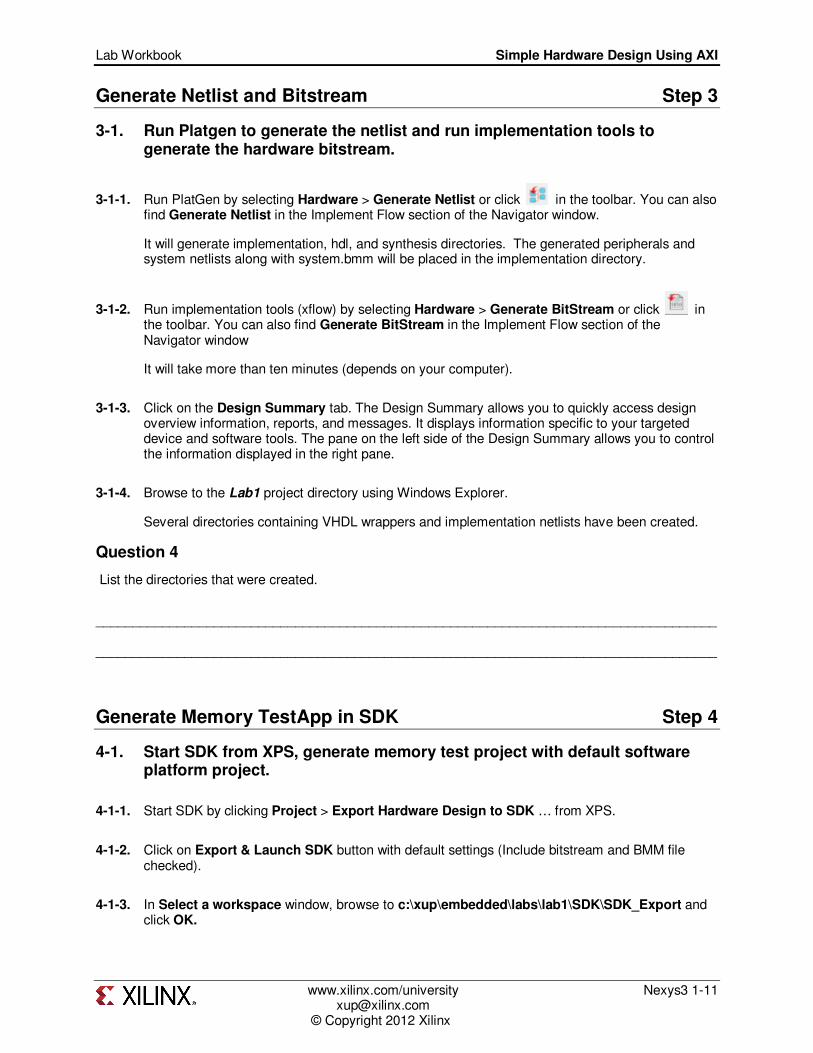
Figure 13. Creating Default Board Support Package
The memory_tests_0 project will be created in the Project Explorer window of SDK.
Test in Hardware Step 5
5-1. Connect and power up the board. Establish the serial communication using SDK’s Terminal tab. Program the FPGA and verify the functionality.
5-1-1. Connect and power up the Nexys3 Board.
5-1-2. Select the tab. If it is not visible then select Window > Show view > Terminal.
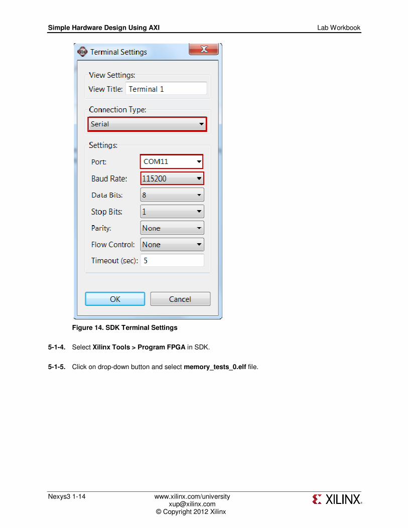
5-1-3. Click on and select appropriate COM port (depends on your computer), and configure it with the parameters as shown.
Simple Hardware Design Using AXI Lab Workbook
Nexys3 1-14 www.xilinx.com/university [email protected] © Copyright 2012 Xilinx
Figure 14. SDK Terminal Settings
5-1-4. Select Xilinx Tools > Program FPGA in SDK.
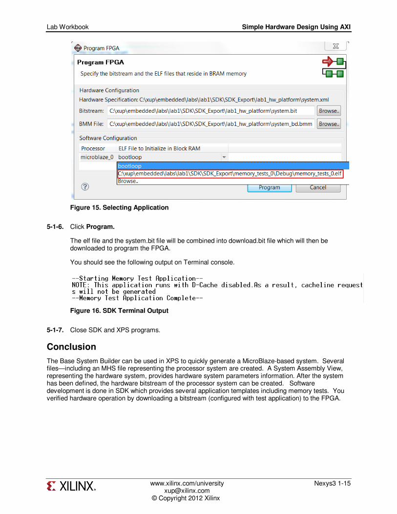
5-1-5. Click on drop-down button and select memory_tests_0.elf file.
Lab Workbook Simple Hardware Design Using AXI
www.xilinx.com/university Nexys3 1-15 [email protected] © Copyright 2012 Xilinx
Figure 15. Selecting Application
5-1-6. Click Program.
The elf file and the system.bit file will be combined into download.bit file which will then be downloaded to program the FPGA.
You should see the following output on Terminal console.
Figure 16. SDK Terminal Output
5-1-7. Close SDK and XPS programs.
Conclusion
The Base System Builder can be used in XPS to quickly generate a MicroBlaze-based system. Several files—including an MHS file representing the processor system are created. A System Assembly View, representing the hardware system, provides hardware system parameters information. After the system has been defined, the hardware bitstream of the processor system can be created. Software development is done in SDK which provides several application templates including memory tests. You verified hardware operation by downloading a bitstream (configured with test application) to the FPGA.

Simple Hardware Design Using AXI Lab Workbook
Nexys3 1-16 www.xilinx.com/university [email protected] © Copyright 2012 Xilinx
Answers
1. List the interface (bus name) instances to the following peripherals: debug_module: axi4lite_0 RS232_Uart_1: axi4lit_0
2. List the nets which are connected to the following ports:
RS232_Uart_1– (IO_IF) uart_0 – RX: RS232_Uart_1_sin RS232_Uart_1– (IO_IF) uart_0 – TX: RS232_Uart_1_sout
3. Select Addresses filter and list the address for the following instances:
RS232_Uart_1– Base address: 0x40600000 RS232_Uart_1– High address: 0x4060ffff microblaze_0_d_bram_ctrl – Base address: 0x00000000 microblaze_0_d_bram_ctrl – High address: 0x00003fff microblaze_0_i_bram_ctrl – Base address: 0x00000000 microblaze_0_i_bram_ctrl – High address: 0x00003fff
4. List the directories that were created.
• __xps
• blockdiagram
• data • etc
• hdl
• implementation • pcores
• synthesis
Lab Workbook Simple Hardware Design Using AXI
www.xilinx.com/university Nexys3 1-17 [email protected] © Copyright 2012 Xilinx
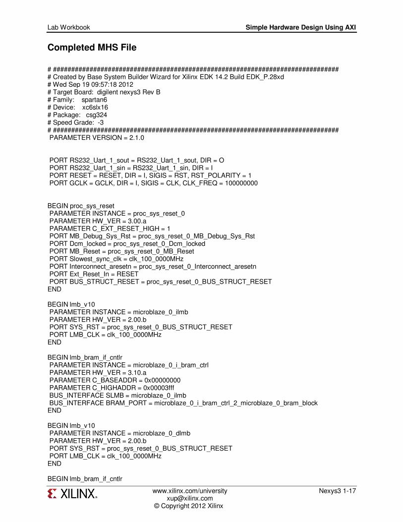
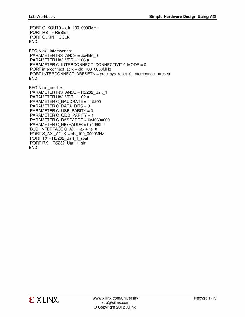
Completed MHS File
# ############################################################################## # Created by Base System Builder Wizard for Xilinx EDK 14.2 Build EDK_P.28xd # Wed Sep 19 09:57:18 2012 # Target Board: digilent nexys3 Rev B # Family: spartan6 # Device: xc6slx16 # Package: csg324 # Speed Grade: -3 # ############################################################################## PARAMETER VERSION = 2.1.0 PORT RS232_Uart_1_sout = RS232_Uart_1_sout, DIR = O PORT RS232_Uart_1_sin = RS232_Uart_1_sin, DIR = I PORT RESET = RESET, DIR = I, SIGIS = RST, RST_POLARITY = 1 PORT GCLK = GCLK, DIR = I, SIGIS = CLK, CLK_FREQ = 100000000 BEGIN proc_sys_reset PARAMETER INSTANCE = proc_sys_reset_0 PARAMETER HW_VER = 3.00.a PARAMETER C_EXT_RESET_HIGH = 1 PORT MB_Debug_Sys_Rst = proc_sys_reset_0_MB_Debug_Sys_Rst PORT Dcm_locked = proc_sys_reset_0_Dcm_locked PORT MB_Reset = proc_sys_reset_0_MB_Reset PORT Slowest_sync_clk = clk_100_0000MHz PORT Interconnect_aresetn = proc_sys_reset_0_Interconnect_aresetn PORT Ext_Reset_In = RESET PORT BUS_STRUCT_RESET = proc_sys_reset_0_BUS_STRUCT_RESET END BEGIN lmb_v10 PARAMETER INSTANCE = microblaze_0_ilmb PARAMETER HW_VER = 2.00.b PORT SYS_RST = proc_sys_reset_0_BUS_STRUCT_RESET PORT LMB_CLK = clk_100_0000MHz END BEGIN lmb_bram_if_cntlr PARAMETER INSTANCE = microblaze_0_i_bram_ctrl PARAMETER HW_VER = 3.10.a PARAMETER C_BASEADDR = 0x00000000 PARAMETER C_HIGHADDR = 0x00003fff BUS_INTERFACE SLMB = microblaze_0_ilmb BUS_INTERFACE BRAM_PORT = microblaze_0_i_bram_ctrl_2_microblaze_0_bram_block END BEGIN lmb_v10 PARAMETER INSTANCE = microblaze_0_dlmb PARAMETER HW_VER = 2.00.b PORT SYS_RST = proc_sys_reset_0_BUS_STRUCT_RESET PORT LMB_CLK = clk_100_0000MHz END BEGIN lmb_bram_if_cntlr
Simple Hardware Design Using AXI Lab Workbook
Nexys3 1-18 www.xilinx.com/university [email protected] © Copyright 2012 Xilinx
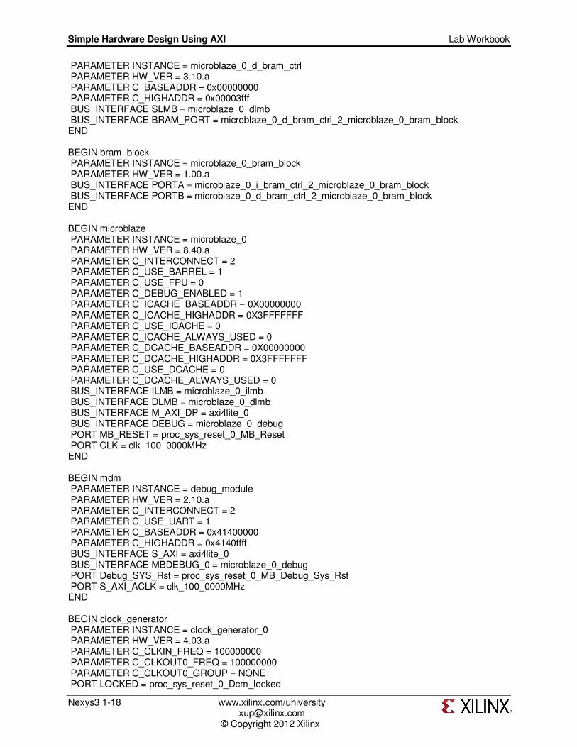
PARAMETER INSTANCE = microblaze_0_d_bram_ctrl PARAMETER HW_VER = 3.10.a PARAMETER C_BASEADDR = 0x00000000 PARAMETER C_HIGHADDR = 0x00003fff BUS_INTERFACE SLMB = microblaze_0_dlmb BUS_INTERFACE BRAM_PORT = microblaze_0_d_bram_ctrl_2_microblaze_0_bram_block END BEGIN bram_block PARAMETER INSTANCE = microblaze_0_bram_block PARAMETER HW_VER = 1.00.a BUS_INTERFACE PORTA = microblaze_0_i_bram_ctrl_2_microblaze_0_bram_block BUS_INTERFACE PORTB = microblaze_0_d_bram_ctrl_2_microblaze_0_bram_block END BEGIN microblaze PARAMETER INSTANCE = microblaze_0 PARAMETER HW_VER = 8.40.a PARAMETER C_INTERCONNECT = 2 PARAMETER C_USE_BARREL = 1 PARAMETER C_USE_FPU = 0 PARAMETER C_DEBUG_ENABLED = 1 PARAMETER C_ICACHE_BASEADDR = 0X00000000 PARAMETER C_ICACHE_HIGHADDR = 0X3FFFFFFF PARAMETER C_USE_ICACHE = 0 PARAMETER C_ICACHE_ALWAYS_USED = 0 PARAMETER C_DCACHE_BASEADDR = 0X00000000 PARAMETER C_DCACHE_HIGHADDR = 0X3FFFFFFF PARAMETER C_USE_DCACHE = 0 PARAMETER C_DCACHE_ALWAYS_USED = 0 BUS_INTERFACE ILMB = microblaze_0_ilmb BUS_INTERFACE DLMB = microblaze_0_dlmb BUS_INTERFACE M_AXI_DP = axi4lite_0 BUS_INTERFACE DEBUG = microblaze_0_debug PORT MB_RESET = proc_sys_reset_0_MB_Reset PORT CLK = clk_100_0000MHz END BEGIN mdm PARAMETER INSTANCE = debug_module PARAMETER HW_VER = 2.10.a PARAMETER C_INTERCONNECT = 2 PARAMETER C_USE_UART = 1 PARAMETER C_BASEADDR = 0x41400000 PARAMETER C_HIGHADDR = 0x4140ffff BUS_INTERFACE S_AXI = axi4lite_0 BUS_INTERFACE MBDEBUG_0 = microblaze_0_debug PORT Debug_SYS_Rst = proc_sys_reset_0_MB_Debug_Sys_Rst PORT S_AXI_ACLK = clk_100_0000MHz END BEGIN clock_generator PARAMETER INSTANCE = clock_generator_0 PARAMETER HW_VER = 4.03.a PARAMETER C_CLKIN_FREQ = 100000000 PARAMETER C_CLKOUT0_FREQ = 100000000 PARAMETER C_CLKOUT0_GROUP = NONE PORT LOCKED = proc_sys_reset_0_Dcm_locked
Lab Workbook Simple Hardware Design Using AXI
www.xilinx.com/university Nexys3 1-19 [email protected] © Copyright 2012 Xilinx
PORT CLKOUT0 = clk_100_0000MHz PORT RST = RESET PORT CLKIN = GCLK END BEGIN axi_interconnect PARAMETER INSTANCE = axi4lite_0 PARAMETER HW_VER = 1.06.a PARAMETER C_INTERCONNECT_CONNECTIVITY_MODE = 0 PORT interconnect_aclk = clk_100_0000MHz PORT INTERCONNECT_ARESETN = proc_sys_reset_0_Interconnect_aresetn END BEGIN axi_uartlite PARAMETER INSTANCE = RS232_Uart_1 PARAMETER HW_VER = 1.02.a PARAMETER C_BAUDRATE = 115200 PARAMETER C_DATA_BITS = 8 PARAMETER C_USE_PARITY = 0 PARAMETER C_ODD_PARITY = 1 PARAMETER C_BASEADDR = 0x40600000 PARAMETER C_HIGHADDR = 0x4060ffff BUS_INTERFACE S_AXI = axi4lite_0 PORT S_AXI_ACLK = clk_100_0000MHz PORT TX = RS232_Uart_1_sout PORT RX = RS232_Uart_1_sin END


![AXI Protocol Checker v1 - Xilinx · The AXI Protocol Checker core monitors AXI interfaces. When attached to an interface, it ... See ARM AMBA® AXI Protocol v2.0 [Ref 1]. Performance](https://img.pdfslide.net/doc/110x75/5b158bc17f8b9ac7128d1298/axi-protocol-checker-v1-xilinx-the-axi-protocol-checker-core-monitors-axi.jpg)