Embed Size (px)
Citation preview
Simulations of long-range surface plasmon polariton waveguides and devices
Pétur Gordon Hermannsson
Faculty of Physical SciencesUniversity of Iceland
2009

Simulations of long-range surface plasmonpolariton waveguides and devices
Pétur Gordon Hermannsson
60 ECTS thesis submitted in partial fulfillment of aMagister Scientiarum degree in Physics
AdvisorDr. Kristján Leósson
Faculty RepresentativeProf. Snorri Ingvarsson
M.Sc. committeeDr. Kristján Leósson
Prof. Hafliði P. Gíslason
Faculty of Physical SciencesSchool of Engineering and Natural Sciences
University of IcelandReykjavík, June 2009

Simulations of long-range surface plasmon polariton waveguides and devices60 ECTS thesis submitted in partial fulfillment of a Magister Scientiarumdegree in Physics
Copyright c© 2009 Pétur Gordon HermannssonAll rights reserved
Faculty of Physical SciencesSchool of Engineering and Natural SciencesUniversity of IcelandVRII, Hjarðarhagi 2-6107, ReykjavíkIceland
Telephone: +354 525 4700
Bibliographic information:Pétur Gordon Hermannsson, 2009, Simulations of long-range surface plasmonpolariton waveguides and devices, Master’s thesis, Faculty of Physical Sciences,University of Iceland.
ISBN 978-9979-9953-0-2
Printing: Háskólaprent, Fálkagata 2, 107 ReykjavíkReykjavík, Iceland, June 2009


Abstract
The properties of long-range surface plasmon polariton waveguides and devicesare investigated using the finite element method. In particular, the opticalmodes of gold stripes and nanowires embedded in a polymer cladding are an-alyzed as well as how the modes are affected by the waveguide geometry andthe resistive heating of the waveguides by a current being passed through themetal cores. This influence of heating on the optical modes can be utilized torealize several active waveguide components, such as variable optical attenu-ators, adjustable multimode interferometers and directional coupler switches,which are studied in detail. The cross-sectional geometry of the stripe andnanowire waveguides are optimized with respect to coupling to standard sin-gle mode optical fibers and waveguide insertion loss. The effect of heating onpropagation loss and coupling loss is investigated and transient analysis of theheat transfer is carried out in order to calculate the response times of activedevice components. The mechanism of attenuation in variable optical attenua-tors is studied and it is demonstrated how the mode interference in multimodeinterferometers may be altered by heating in order to realize switching. Theinfluence of cladding geometry on the performance of nanowire waveguides isinvestigated as well as their tolerance to fabrication errors.

Útdráttur
Eiginleikar ljósrása fyrir langsæknar rafgasbylgjur eru kannaðir með búta-aðferð. Sér í lagi eru sveifluhættir ljósrása sem byggja á málmræmum ognanóvírum úr gulli í fjölliðuklæðningu rannsakaðir ásamt því hvernig lögunmálmanna og upphitun þeirra með rafstraumi hefur áhrif á sveifluhættina.Þessi tengsl sveifluhátta við upphitun má nota til að búa til virkar ljósrásir áborð við stillanlega ljósdeyfara, fjölháttavíxlrásir og stefnutengja, og eru þærrannsakaðar hér. Sú þykkt og breidd málmræmanna og nanovíranna sem lág-markar bæði tapið í ljósrásunum og tapið sem verður þegar ljós er flutt úrhefðbundnum ljósleiðara yfir í ljósrásina er reiknuð. Einnig eru áhrif upphit-unar á útbreiðslutap og flutningstap rannsökuð og eru tímaháðir útreikningargerðir til að finna viðbragðstíma virku ljósrásanna. Deyfingin í stillanlegumljósdeyfurum er rannsökuð ásamt því hvernig nota megi upphitun til að breytasamliðunarmynstri í fjölháttavíxlrásum og flytja þannig ljósið frá einni út-gangsrás yfir á aðra. Áhrif breiddar og þykktar fjölliðuklæðningarinnar áafkastagetu ljósrása úr nanóvírum er könnuð ásamt þoli þeirra gagnvart fram-leiðslugöllum.


Contents
List of Figures xi
List of Tables xv
Acknowledgements xvii
1 Introduction 1
2 Theory 52.1 Maxwell’s equations . . . . . . . . . . . . . . . . . . . . . . . . . 52.2 The Helmholtz wave equation . . . . . . . . . . . . . . . . . . . 72.3 The Drude model . . . . . . . . . . . . . . . . . . . . . . . . . . 72.4 The complex refractive index . . . . . . . . . . . . . . . . . . . . 112.5 Surface plasmon polaritons . . . . . . . . . . . . . . . . . . . . . 12
2.5.1 TM modes . . . . . . . . . . . . . . . . . . . . . . . . . . 142.5.2 TE modes . . . . . . . . . . . . . . . . . . . . . . . . . . 162.5.3 Energy confinement and propagation distance . . . . . . 17
2.6 Long range surface plasmon polaritons . . . . . . . . . . . . . . 18
3 Modeling 273.1 The finite element method and COMSOL . . . . . . . . . . . . . 273.2 PDEs and boundary conditions . . . . . . . . . . . . . . . . . . 30
3.2.1 Heat transfer . . . . . . . . . . . . . . . . . . . . . . . . 303.2.2 Eigenmode analysis . . . . . . . . . . . . . . . . . . . . . 31
3.3 Meshing . . . . . . . . . . . . . . . . . . . . . . . . . . . . . . . 323.4 Application to heated plasmonic waveguides . . . . . . . . . . . 34
ix

3.4.1 Temperature dependent material properties . . . . . . . 343.4.2 The modeling of heated waveguides . . . . . . . . . . . . 38
4 Stripe waveguides 434.1 Fabrication . . . . . . . . . . . . . . . . . . . . . . . . . . . . . 434.2 Optimization . . . . . . . . . . . . . . . . . . . . . . . . . . . . 444.3 Heat transfer calculations . . . . . . . . . . . . . . . . . . . . . 484.4 Variable optical attenuators . . . . . . . . . . . . . . . . . . . . 504.5 Directional couplers . . . . . . . . . . . . . . . . . . . . . . . . . 544.6 Multimode interferometers . . . . . . . . . . . . . . . . . . . . . 56
5 Nanowire waveguides 635.1 Introduction . . . . . . . . . . . . . . . . . . . . . . . . . . . . . 635.2 Fabrication . . . . . . . . . . . . . . . . . . . . . . . . . . . . . 655.3 Optimization . . . . . . . . . . . . . . . . . . . . . . . . . . . . 665.4 The influence of cladding on performance . . . . . . . . . . . . . 685.5 The influence of asymmetry on performance . . . . . . . . . . . 695.6 Heated nanowires . . . . . . . . . . . . . . . . . . . . . . . . . . 71
6 Conclusion and discussion 75
Bibliography 79
x

List of Figures
2.1 The reflectance of copper and gold according to the Drude model. 102.2 The real and imaginary part of the complex refractive index of
the noble metals. . . . . . . . . . . . . . . . . . . . . . . . . . . 112.3 An electromagnetic wave propagating along the interface be-
tween two media. . . . . . . . . . . . . . . . . . . . . . . . . . . 122.4 The dispersion relations of SPPs propagating along the interface
between a Drude metal and air and glass. . . . . . . . . . . . . . 152.5 The calculated evanescent decay length and propagation length
for an interface between silver and air. . . . . . . . . . . . . . . 182.6 Surface plasmon polaritons propagating along both sides of a film. 182.7 The electric field components of the symmetric mode. . . . . . . 212.8 The electric field components of the antisymmetric mode. . . . . 222.9 The dispersion relation of the symmetric and antisymmetric
modes for a 50 nm thick silver film in air. . . . . . . . . . . . . . 232.10 The behavior of the propagation constant β as a function of film
thickness d for a gold film embedded in BCB. . . . . . . . . . . 24
3.1 An illustration of the difference between a triangular and aquadrilateral mesh. . . . . . . . . . . . . . . . . . . . . . . . . . 33
3.2 The meshed geometry of a stripe waveguide. . . . . . . . . . . . 343.3 The density and thermal conductivity of air as a function of
temperature. . . . . . . . . . . . . . . . . . . . . . . . . . . . . . 353.4 The thermal conductivity and heat capacity of gold as a function
of temperature. . . . . . . . . . . . . . . . . . . . . . . . . . . . 363.5 The thermal conductivity of BCB as a function of temperature. 36
xi
3.6 The refractive index of BCB as a function of wavelength. . . . . 373.7 The temperature profiles of a gold stripe heated with asymmet-
ric and symmetric cooling conditions. . . . . . . . . . . . . . . . 40
4.1 The fabrication process for LR-SPP waveguides. . . . . . . . . . 444.2 An illustration of a LR-SPP stripe waveguide embedded in a
polymer. . . . . . . . . . . . . . . . . . . . . . . . . . . . . . . . 444.3 The simulated and measured cross-sectional intensity profiles of
a LR-SPP mode. . . . . . . . . . . . . . . . . . . . . . . . . . . 454.4 The calculated coupling loss, propagation loss and insertion loss
for 1 mm long gold stripe waveguides embedded in BCB at λ =
1064 nm and λ = 1550 nm. . . . . . . . . . . . . . . . . . . . . 464.5 The calculated intensity profiles along the x-axis compared to
measurements on a 10 nm thick, 10.5 µm and 4.5 µm widewaveguide. . . . . . . . . . . . . . . . . . . . . . . . . . . . . . . 47
4.6 The cross-sectional temperature profiles for LR-SPP waveguidesin a single and double heatsink configuration, including intensityprofiles of the LR-SPP modes. . . . . . . . . . . . . . . . . . . . 49
4.7 The asymmetry of the LR-SPP mode for a heat dissipation of50 mW/mm and asymmetric cooling conditions. . . . . . . . . . 49
4.8 An illustration of a LR-SPP waveguide with contact pads. . . . 504.9 The heating of the waveguide leads to a decrease in the real part
of the effective mode index of the LR-SPP mode. . . . . . . . . 514.10 The measured extinction ratio of a variable optical attenuator
made from a 6 µm wide and 16 nm thick gold stripe with a totallength of 2 mm and a 1 mm heated section. . . . . . . . . . . . 52
4.11 Heating the waveguide leads to increased coupling loss and in-sertion loss, while decreasing the propagation. . . . . . . . . . . 53
4.12 The calculated temporal response of a 15 nm thick and 8 µmwide gold waveguide in BCB heated with an applied power of50 mW/mm. . . . . . . . . . . . . . . . . . . . . . . . . . . . . . 54
4.13 A schematic illustration of a directional coupler. . . . . . . . . . 54
xii
4.14 The symmetric and antisymmetric supermodes for two 4 µmwide and 13 nm thick gold stripes embedded in BCB, separatedby 2 µm. . . . . . . . . . . . . . . . . . . . . . . . . . . . . . . . 55
4.15 The calculated coupling length as a function of waveguide sep-aration for two different wavelengths. . . . . . . . . . . . . . . . 56
4.16 An illustration of a tunable multimode interferometer. . . . . . . 574.17 The normalized effective mode indices and propagation loss ver-
sus waveguide width for a 15 nm thick stripe at λ = 1550 nm. . 574.18 A schematic illustration of the MMI structure studied. . . . . . 584.19 The modes supported by a WMMI = 40 µm wide MMI device
for three different applied heating powers along with the changein effective mode index with increased heating. . . . . . . . . . . 59
4.20 Temperature profile of the heated MMI, as determined in COM-SOL. . . . . . . . . . . . . . . . . . . . . . . . . . . . . . . . . . 60
4.21 The calculated intensity of a LR-SPP mode at λ = 1550 nmpropagating through a 40 µm wide and 2.45 mm long MMIwith and without 60 mW/mm of applied heating power. . . . . 60
5.1 An illustration of the electric field of a fundamental plasmonmode supported by an isolated corner. . . . . . . . . . . . . . . 63
5.2 The electric field of the four supermodes arising from the cou-pling of corner modes. . . . . . . . . . . . . . . . . . . . . . . . 64
5.3 The calculated magnitude and direction of the electric field ofthe E(0,1) polarized mode in the vicinity of a 180 nm wide goldnanowire in BCB. . . . . . . . . . . . . . . . . . . . . . . . . . . 65
5.4 The simulated supermodes of a 150 nm wide nanowire made ofgold at a wavelength of λ = 1550 nm. . . . . . . . . . . . . . . . 66
5.5 The calculated coupling loss, propagation loss and fiber-to-fiberinsertion loss for 0.5, 1 and 2 mm long gold nanowire waveguidesin a 20 µm thick layer of BCB at λ = 1550 nm. . . . . . . . . . 67
5.6 The coupling loss and propagation loss in symmetric nanowirewaveguides for three different cladding thicknesses. . . . . . . . 68
xiii
5.7 The total insertion loss for different lengths of 180 nm widesymmetric nanowire waveguides when the extent of the dielec-tric cladding layer is limited vertically and both vertically andhorizontally. . . . . . . . . . . . . . . . . . . . . . . . . . . . . . 69
5.8 The propagation loss and coupling loss in asymmetric nanowirewaveguides. . . . . . . . . . . . . . . . . . . . . . . . . . . . . . 70
5.9 Trapezoidal deformation of the nanowire can result in significantpolarization dependent loss. . . . . . . . . . . . . . . . . . . . . 71
5.10 The real part of the effective mode index for the E(0,1) polar-ization versus heating power for a gold nanowire in BCB atλ = 1550 nm. . . . . . . . . . . . . . . . . . . . . . . . . . . . . 72
5.11 Heating the waveguide leads to increased coupling loss and in-sertion loss. The propagation loss decreases however. . . . . . . 73
xiv

List of Tables
2.1 The free electron densities, relaxation times and correspondingplasma frequency of the noble metals at room temperature. . . . 10
xv

xvi

Acknowledgements
I would like to start by expressing my deepest gratitude towards my advisorDr. Kristján Leósson for his invaluable guidance throughout the duration ofthis work. I have found myself in the unique position of having almost unlim-ited access to my supervisor, something which is exceptionally rare in mostacademic circles. I would also like to thank Tiberiu Rosenzveig for his collab-oration and experimental assistance as well as my other fellow group members.
I am also extremely grateful to my dear wife Gunnur Ýr for her loving supportand understanding during the writing this thesis. I also thank my parents andfamily for their help and kind encouragement throughout my studies.
This project was partially supported by the Icelandic Research Fund and theIcelandic Research Fund for Graduate Students.
xvii

xviii
1 Introduction
The surge in optical telecommunication in recent years has led to extensive re-search in the field of integrated optical circuits with the purpose of minimizingdevice components, reducing cost and realizing various functionalities such asoptical routing, splitting etc. Although there is currently no technology thatcan match optical fibers in transmitting signals over vast distances with lowloss, there are however numerous technologies available for guiding over shorterregions, each geared to a particular set of applications. These include waveg-uides based on semiconductors, polymers, ceramic films and others. However,in recent years more exotic methods of guiding light have been investigated,such as photonic crystal and long-range surface plasmon polaritons waveguides.
It has long been known that an interface between a metal and a dielectricis able to sustain a propagating electromagnetic wave in the form of a surfaceplasmon polariton (SPP), which arises from interaction between free electronsin the metal and electromagnetic radiation. The most attractive feature ofSPPs over conventional dielectric devices is their ability to confine light tobelow the diffraction limit and realize high field intensities in relatively smallvolumes. However, due to SPPs being associated with the interface of a metal,a highly lossy material at optical wavelengths, they can only achieve propa-gation distances of micrometers and have thus not been considered realisticcandidates for waveguiding. Instead, they are well suited for sensing applica-tions: the tightly bound nature of SPPs makes them particularly sensitive tochanges in refractive index at surfaces [1] and their high field intensities havebeen employed for example in surface enhanced Raman spectroscopy for singlemolecule detection [2].
By replacing the single interface with a thin metal film sandwiched betweentwo dielectric layers, the SPPs propagating at each interface can couple to forma symmetric mode, called a long-range surface plasmon polariton (LR-SPP)[3]. As the metal film thickness decreases, the mode evolves into a plane wavein the dielectric, leading to decreased confinement and longer propagation dis-tances. For film thicknesses of the order of 10 nm, propagation distances oftens of millimeters can be achieved at optical wavelengths [4]. Wide metalfilms are however not suitable for waveguiding since they offer no lateral fieldconfinement and metal stripes (width � thickness) are therefore used instead[5]. Furthermore, by adjusting the cross-sectional dimensions of the stripes,
1
the shape of the fundamental mode can be tuned to closely match that ofa standard single mode optical fiber [5, 6, 7], facilitating efficient excitationby end-fire coupling. A number of passive devices and devices componentsbased on LR-SPP waveguides have been experimentally demonstrated, includ-ing S-bends, Y-splitters, multimode interferometer devices and directional cou-plers [8]. However, the main advantage of metal LR-SPP waveguides lies intheir ability to conduct an electrical current. By embedding the stripes incladdings with suitable thermo-optic coefficients and resistively heating them,the propagating modes can be altered in order to realize power efficient activedevices, such as thermo-optic Mach–Zehnder interferometric modulators anddirectional coupler switches [9].
Unfortunately, metal films and stripes are only capable of guiding electricfields with the main field component perpendicular to the film. This strongpolarization dependence of stripe waveguide components renders them largelyincompatible with established integrated optical devices and fibers. In order toaddress this issue, it has been shown [10, 11, 12] that square metallic nanowires(typically with sidelengths of the order of ∼200 nm) can support two perpen-dicularly polarized long-range supermodes and are thus capable of guiding anypolarization of light. These supermodes are formed by specific superpositionsof plasmon polariton modes that propagate along the corners of the nanowireand can also be efficiently excited by end-fire coupling [12].
Many of the reported SPP devices have been made of gold stripes or nanowiressandwiched between two equally thick layers of the polymer benzocyclobutene(BCB) supported by a silicon substrate. The use of gold is mainly due toits suitable optical properties at telecommunication wavelengths (around λ =1550 nm) and the fact that it doesn’t form oxides or other compounds at itssurface. In order to create power efficient active devices, cladding materialswith fairly large (negative) thermo-optic responses are required which makespolymers more suitable than other dielectrics such as glass. Despite other poly-mers perhaps being more advantageous, BCB has been used in part becauseof its ease of use and its simple processing, chemical resistance and relativelyhigh glass transition temperature [13] which enables the devices to withstandgreater temperatures.
In this thesis the properties of long-range surface plasmon polariton waveg-uides and devices are investigated using the finite element method. In par-ticular, the optical modes of gold stripes and nanowires embedded in BCBare analyzed as well as how the modes are affected by the waveguide geome-
2

try and the resistive heating of the waveguides due to a current being passedthrough the metal cores. Several active devices based on this principle areexamined, such as the variable optical attenuator, multimode interferometerand directional coupler. The thesis is organized as follows: first, the behav-ior of LR-SPPs is theoretically analyzed, followed by a discussion on how thefinite element method was used to simulate the waveguides. The results ofthe simulations are split into two separate chapters, the first dealing with thestripe waveguides and devices and the second with the nanowires. The thesisthen ends with a summary and a few concluding remarks regarding the futureof LR-SPP research and possible applications.
3

4
2 Theory
This chapter lays the theoretical groundwork needed to understand the behav-ior of long-range surface plasmon polaritons. Starting off with the Maxwell’sequations, the necessary equations are derived. The reader is then introducedto the concept of the complex permittivity, and its behavior is investigatedwith the help of the Drude model of conductivity. Next, following a briefdiscussion on plasmons, a theoretical analysis is given to the properties of sur-face plasmon polaritons propagating along an interface between a metal anda dielectric material. Following a similar approach for the case of a doubleinterface, it is shown how the coupling of surface plasmon polaritons on eachinterface gives rise to long range surface plasmon polaritons.
But as with most discussions on electromagnetic phenomena, we start withthe Maxwell’s equations.
2.1 Maxwell’s equationsThe Maxwell’s equations are a set of four partial differential equations that canbe used to explain all macroscopic electromagnetic phenomena [14]. These canbe applied to the interaction of electromagnetic fields with metals of sizes downto a few nanometers without having to resort to the full arsenal of quantummechanics. This is due to the minute spacing of the energy levels of theconduction electrons compared to the thermal energy at room temperature[15]. The Maxwell’s equations are as follows
∇ ·D = ρf (2.1)∇ ·B = 0 (2.2)
∇× E = −∂B∂t
(2.3)
∇×H = Jf +∂D
∂t(2.4)
where D is the electric displacement, E is the electric field, B is the magneticfield and H is the magnetizing field. These four partial differential equationsrelate the electric and magnetic fields to their sources: the volume chargedensity of free charges ρf and the density of free current Jf . Furthermore, thefields are linked via the volume density of electric dipole moment P and the
5
volume density of magnetic dipole moment M by
D = ε0E+P (2.5)
H =1
µ0
B−M (2.6)
where ε0 and µ0 are the electric permittivity and magnetic permeability ofvacuum. In the case of linear and isotropic media the polarization and mag-netization vectors P and M can be written as
P = ε0χeE (2.7)M = χmH (2.8)
where χe and χm are the electric and magnetic susceptibility of the medium.The electric displacement and magnetic field can then be written as
D = ε0 (1 + χe)E (2.9)= εE (2.10)
and
B = µ0 (1 + χm)H (2.11)= µH (2.12)
where ε and µ denote the permittivity and permeability of the medium. There-fore, in the case of linear and isotropic media the Maxwell’s equations become
∇ · E =ρf
ε(2.13)
∇ ·B = 0 (2.14)
∇× E = −∂B∂t
(2.15)
∇×B = µJf + µε∂E
∂t(2.16)
Another important constitutive relationship is Ohm’s law, which relates thecurrent density Jf to the electric field E via the conductivity of the materialσ by
Jf = σE (2.17)
6
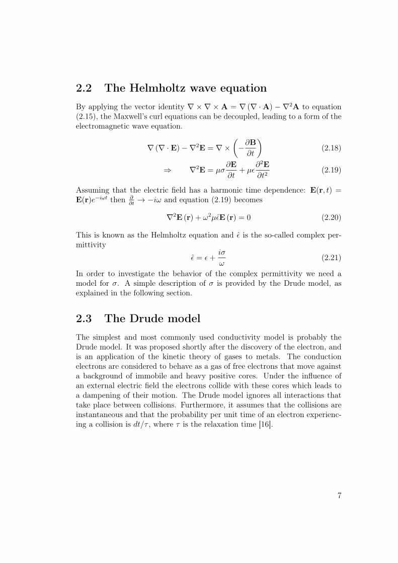
2.2 The Helmholtz wave equationBy applying the vector identity ∇ ×∇ ×A = ∇ (∇ ·A) − ∇2A to equation(2.15), the Maxwell’s curl equations can be decoupled, leading to a form of theelectromagnetic wave equation.
∇ (∇ · E)−∇2E = ∇×(−∂B∂t
)(2.18)
⇒ ∇2E = µσ∂E
∂t+ µε
∂2E
∂t2(2.19)
Assuming that the electric field has a harmonic time dependence: E(r, t) =E(r)e−iωt then ∂
∂t→ −iω and equation (2.19) becomes
∇2E (r) + ω2µεE (r) = 0 (2.20)
This is known as the Helmholtz equation and ε is the so-called complex per-mittivity
ε = ε+iσ
ω(2.21)
In order to investigate the behavior of the complex permittivity we need amodel for σ. A simple description of σ is provided by the Drude model, asexplained in the following section.
2.3 The Drude modelThe simplest and most commonly used conductivity model is probably theDrude model. It was proposed shortly after the discovery of the electron, andis an application of the kinetic theory of gases to metals. The conductionelectrons are considered to behave as a gas of free electrons that move againsta background of immobile and heavy positive cores. Under the influence ofan external electric field the electrons collide with these cores which leads toa dampening of their motion. The Drude model ignores all interactions thattake place between collisions. Furthermore, it assumes that the collisions areinstantaneous and that the probability per unit time of an electron experienc-ing a collision is dt/τ , where τ is the relaxation time [16].
7
The equation of motion governing the motion of individual electrons is [16]1
m∗dv(t)
dt= −m
∗
τv(t)− eE(t) (2.22)
where m∗ is the effective mass of the electrons in the crystal and e is theelectronic charge. If the driving field is assumed to have a harmonic timedependence, E(t) = E0e
−iωt then equation (2.22) will have a solution of theform v(t) = v0e
−iωt. Substituting E(t) into equation (2.22) yields a meanvelocity of
v(t) = − eτ
m∗(1− iωτ)E(t) (2.23)
The current density is related to the mean velocity of the electrons accordingto Jf = −nev, where n is the number of conduction electrons per unit volume.Therefore
Jf =ne2τ
m∗(1− iωτ)E(t) (2.24)
and comparison with Ohm’s law (2.17) gives
σ =ne2τ
m∗(1− iωτ)(2.25)
Using equation (2.21), an expression for the complex permittivity can now begiven
ε = ε−ω2pε0
ω2 + iω/τ(2.26)
where ωp is the plasma frequency
ω2p =
ne2
ε0m∗(2.27)
The first term in equation (2.26) is due to the bound charges in the metal,whereas the second term is due to the free electrons. If the contribution fromthe bound charges is neglected, the relative complex permittivity (εr = ε/ε0)becomes
εr = 1−ω2p
ω2 + iω/τ(2.28)
1This approach ignores the magnetic field component of the external field B, as well asthe field’s r dependence. As explained by ref. [16], the forces due to B are many ordersof magnitude weaker than those due to the electric field E. Furthermore, ignoring the rdependence is safe as long as the field doesn’t vary much over distances comparable withthe mean free path of the electrons.
8
Separating this into real and imaginary parts (εr = ε′r + iε′′r) gives
ε′r = 1−ω2pτ
2
1 + ω2τ 2(2.29)
ε′′r =ω2pτ
ω (1 + ω2τ 2)(2.30)
The relaxation time τ is typically of the order 10−15 to 10−14 seconds at roomtemperature [16]. For visible and shorter wavelengths ωτ � 1 and the realpart may be approximated as
ε′r ≈ 1−ω2p
ω2(2.31)
At frequencies lower than the plasma frequency, ω < ωp, ε′r becomes nega-tive and the solution to the Helmholtz equation (2.20) decays exponentially inspace, leading to the metal being highly reflective. However, when ω > ωp, ε′rbecomes positive and the solution to (2.20) become oscillatory and the metal istransparent. From this we can see that the plasma frequency may therefore beinterpreted as the frequency at which the metal starts becoming transparentto incoming electromagnetic radiation. Furthermore, it can be shown [15, 16]that the plasma frequency corresponds to the characteristic frequency of col-lective longitudinal oscillations of the free electron gas. The quanta of theseplasma oscillations are known as (volume or bulk) plasmons, and due to theirlongitudinal nature, they do not couple to transverse electromagnetic waves.Surface plasmons on the other hand couple readily to photons to form polari-tons, as we shall see later.
The plasma frequency of most metals is in the ultraviolet part of the spec-trum, which explains why they are reflective at visible wavelengths. Table 2.1shows the plasma frequency and the corresponding wavelength for the threenoble metals (copper, silver and gold), as obtained from equation (2.27) usingm∗ = me and data on the free electron densities n and relaxation times τ fromref. [16]. The reflectivity spectrum of gold and copper according to the Drudemodel is shown in figure 2.1, in which the dashed lines indicate the plasmafrequency for each metal.
9
Table 2.1: The free electron densities and relaxation times of the noble metalsat room temperature [16], and the corresponding calculated plasma frequencyand wavelength.
Element n [1022 cm−3] τ [fs] ωp [1016 s−1] λ nmCopper 8.47 27 1.643 115Silver 5.86 40 1.365 138Gold 5.90 30 1.370 138
It is worth pointing out however that the Drude model doesn’t accurately de-scribe the behavior of many metals at high frequencies, as is evident by theapparent difference in color between gold and silver despite having the sameplasma frequency. The alkali metals such as as lithium, sodium and potassiumdo indeed have an almost Drude-like response and become transparent in theultraviolet, but in the case of the noble metals, absorption due to interbandtransitions becomes increasingly important for visible frequencies. Neverthe-less, the Drude model remains popular due to its simplicity and can be easilymodified to correctly describe the optical properties of gold and silver [15]. Forour purposes however, the Drude model in its present form is adequate.
8 0 1 0 0 1 2 0 1 4 0 1 6 0 4 0 0 6 0 0 8 0 00 , 0
0 , 2
0 , 4
0 , 6
0 , 8
1 , 0 C o p p e r G o l d
Refle
ctivity
W a v e l e n g t h [ n m ]
V i s i b l es p e c t r u m
Figure 2.1: The reflectance of copper and gold according to the Drude model.
10
2.4 The complex refractive indexIt can sometimes be more convenient to use the complex refractive index n =n+iκ instead of the complex permittivity εr = ε′r+iε
′′r . The complex refractive
index is defined as n =√εr, which gives
n2 =
√ε′r
2 + ε′′r2 + ε′r
2(2.32)
κ2 =
√ε′r
2 + ε′′r2 − ε′r
2(2.33)
Here, n corresponds to the traditional index of refraction, while κ is the so-called extinction coefficient and determines the absorption loss of an elec-tromagnetic wave as it propagates through a material. It is related to theabsorption coefficient α of Beer’s law I(z) = I0e
−αz via
α =2κω
c(2.34)
where I is the intensity of a propagating wave, which is attenuated exponen-tially due to the medium. Figure 2.2 shows the real and imaginary componentsof n for the three noble metals.
0 , 0 0 , 2 0 , 4 0 , 6 0 , 8 1 , 0 1 , 2 1 , 4 1 , 6 1 , 8 2 , 00 , 00 , 2
0 , 40 , 6
0 , 81 , 01 , 2
1 , 41 , 6
�
n
�������������
�������� �������
0 , 0 0 , 2 0 , 4 0 , 6 0 , 8 1 , 0 1 , 2 1 , 4 1 , 6 1 , 8 2 , 00
2
4
6
8
1 0
1 2
1 4
1 6
�
W a v e l e n g t h [ n m ]
C o p p e r S i l v e r G o l d
Figure 2.2: The real (left) and imaginary part (right) of the complex refractiveindex of the noble metals. The figure is adapted from data published in ref.[17].
11
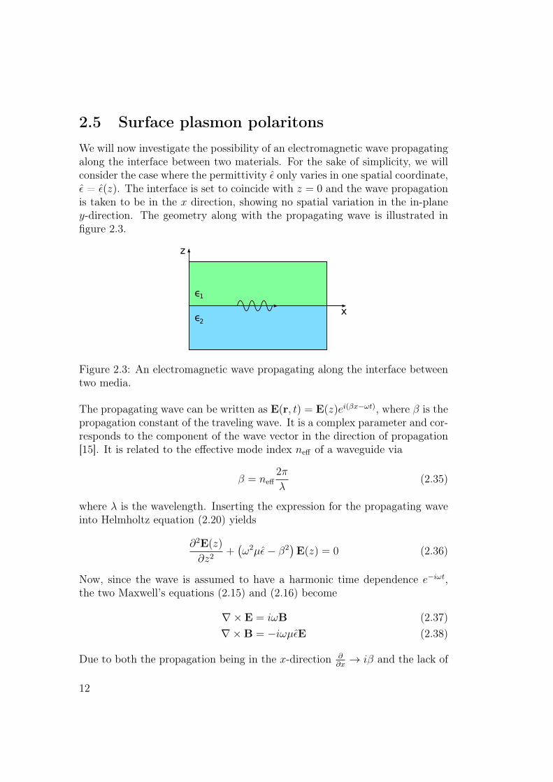
2.5 Surface plasmon polaritonsWe will now investigate the possibility of an electromagnetic wave propagatingalong the interface between two materials. For the sake of simplicity, we willconsider the case where the permittivity ε only varies in one spatial coordinate,ε = ε(z). The interface is set to coincide with z = 0 and the wave propagationis taken to be in the x direction, showing no spatial variation in the in-planey-direction. The geometry along with the propagating wave is illustrated infigure 2.3.
ϵ
ϵ
1
2
z
x
Figure 2.3: An electromagnetic wave propagating along the interface betweentwo media.
The propagating wave can be written as E(r, t) = E(z)ei(βx−ωt), where β is thepropagation constant of the traveling wave. It is a complex parameter and cor-responds to the component of the wave vector in the direction of propagation[15]. It is related to the effective mode index neff of a waveguide via
β = neff2π
λ(2.35)
where λ is the wavelength. Inserting the expression for the propagating waveinto Helmholtz equation (2.20) yields
∂2E(z)
∂z2+(ω2µε− β2
)E(z) = 0 (2.36)
Now, since the wave is assumed to have a harmonic time dependence e−iωt,the two Maxwell’s equations (2.15) and (2.16) become
∇× E = iωB (2.37)∇×B = −iωµεE (2.38)
Due to both the propagation being in the x-direction ∂∂x→ iβ and the lack of
12
spatial variation in the y-direction ∂∂y→ 0, these two curl equations lead to
the following coupled equations:
∂By
∂z= iωµεEx (2.39)
iβBy = −iωµεEz (2.40)∂Ex∂z− iβEz = iωBy (2.41)
∂Ey∂z
= −iωBx (2.42)
iβEy = iωBz (2.43)∂Bx
∂z− iβBz = −iωµεEy (2.44)
According to ref. [15], these equations allow for two sets of self-consistent so-lutions with different polarization properties of the propagating waves. Thefirst three correspond to transverse magnetic (TM) modes, where only thefield components Ex, Ez and By are nonzero, and the last three correspond totransverse electric (TE) modes where only Bx, Bz and Ey are nonzero.
In the case of TM modes, the above equations reduce to
Ex = −i1
ωµε
∂By
∂z(2.45)
Ez = −β
ωµεBy (2.46)
∂2By
∂z2+(ω2µε− β2
)By = 0 (2.47)
whereas in the case of TE modes they reduce to
Bx =i
ω
∂Ey∂z
(2.48)
Bz =β
ωEy (2.49)
∂2Ey∂z2
+(ω2µε− β2
)Ey = 0 (2.50)
Now, having determined the governing equations for both the TE and TMmodes, we are ready to turn our attention back to the problem at hand. We
13
will first examine the properties of a TM polarized wave propagating along theinterface.
2.5.1 TM modes
In the region z > 0, where the permittivity and permeability are ε1 and µ1
respectively, equation (2.47) has the solution By = Ae−k1z, where A is a co-efficient describing the amplitude and k1 is the component of the wave vectorperpendicular to the interface in this medium, k2
1 = β2 − ω2µ1ε1. Tagging onthe propagation factor eiβx then gives
By = Ae−k1zeiβx (2.51)
Furthermore, from equations (2.45) and (2.46) we obtain
Ex = iAk1
ωµ1ε1e−k1zeiβx (2.52)
Ey = −Aβ
ωµ1ε1e−k1zeiβx (2.53)
Similarly, in the region z < 0, we get
By = Bek2zeiβx (2.54)
Ex = −iBk2
ωµ2ε2ek2zeiβx (2.55)
Ey = −Bβ
ωµ2ε2ek2zeiβx (2.56)
where k22 = β2 − ω2µ2ε2 and B is a second amplitude coefficient.
In the absence of a surface current and assuming that both materials arenon-magnetic, µ1 = µ2 = µ0, the tangential field components By and Ex mustbe continuous across the interface. This requires that A = B, and more im-portantly that
k1
k2
= − ε1ε2
(2.57)
In order for the surface wave to be confined to the interface, the real parts ofk1 and k2 must be positive, which in turn requires that the real parts of thecomplex permittivities ε1 and ε2 are opposite in sign. As discussed in section2.3, for most metals the real part of ε becomes negative for visible and longerwavelengths, and thus an interface between a dielectric and a metal satisfies
14
this condition. A confined surface wave propagating along such an interfaceis called a surface plasmon polariton (SPP) and arises via the coupling of theelectromagnetic field to surface plasmons [15] (see below). By combining theexpressions for k1 and k2 with equation (2.57) we obtain the dispersion relationof the SPPs
β =ω
c
√εr1 εr2εr1 + εr2
(2.58)
By assuming that εr1 is real (εr1 = εr1) and that the condition ε′′r2 < |ε′r2| holds
for εr2 = ε′r2 + iε′′r2 , the real and imaginary parts of the propagation constantβ = β′ + iβ′′ can be separated [18]
β′ =ω
c
(εr1ε
′r2
εr1 + ε′r2
)1/2
(2.59)
β′′ =ω
c
(εr1ε
′r2
εr1 + ε′r2
)3/2 ε′′r22(ε′r2)
2(2.60)
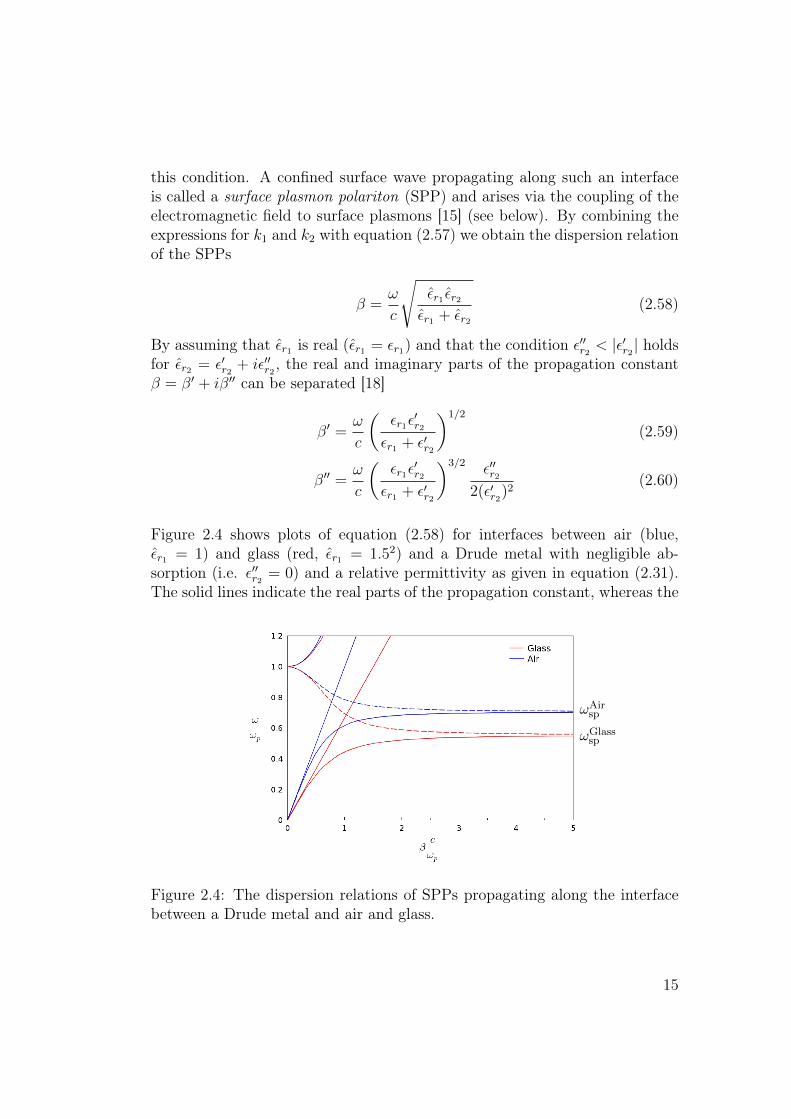
Figure 2.4 shows plots of equation (2.58) for interfaces between air (blue,εr1 = 1) and glass (red, εr1 = 1.52) and a Drude metal with negligible ab-sorption (i.e. ε′′r2 = 0) and a relative permittivity as given in equation (2.31).The solid lines indicate the real parts of the propagation constant, whereas the
ωAirsp
ωGlasssp
Figure 2.4: The dispersion relations of SPPs propagating along the interfacebetween a Drude metal and air and glass.
15
dashed lines indicate the imaginary parts. The straight lines in the figure arethe lightlines, which are the dispersion curves the light would follow were itfree to propagate through the dielectric medium, β0 = (ω/c)
√εr1 . The solid
curves in the upper left corner are the quasibound, leaky modes [15].
As can be seen from figure 2.4, as the frequency decreases the propagationconstant tends to β0 and the SPP mode becomes increasingly less confinedto the interface until it eventually acquires the nature of a grazing-incidencelight field, known as Sommerfeld-Zenneck waves [15]. On the other hand, asthe propagation constant increases, the frequency of the SPPs approaches thecharacteristic surface plasmon frequency
ωsp =ωp√1 + ε1
(2.61)
In this regime, the group velocity vg = dω/dβ → 0 and the mode acquires anelectrostatic character, and is known as a surface plasmon [15].
By inspection of equation (2.58), it can be seen that β > β0, and the disper-sion curves of SPPs always lie to the right of their respective light lines. TheSPPs therefore cannot transform into light and are said to be non-radiative.Conversely, the opposite is also true; SPPs cannot be excited by simply irra-diating the interface with light. Some method of increasing the propagationconstant of the light must be used, such as grating or prism coupling [15, 19]or scattering from surface roughness or defects [15, 18, 20]. A point sourceof SPPs has also been shown to be generated on gold and silver films by theoptical probe of a scanning near-field optical microscope [21].
2.5.2 TE modes
Let us now briefly investigate the case of TE surface modes. In a com-pletely analogous manner as before, equation (2.50) yields a confined wavesolution of the form Ey = A exp(−k1z) exp(iβx) in the region z > 0 andEy = B exp(k2z) exp(iβx) in the region z < 0. Continuity at the boundaryz = 0 demands that A = B. Inserting these expressions into equation (2.48)gives
Bx =
{−A ik1
ωe−k1zeiβx z > 0
A ik2ωek2zeiβx z < 0
(2.62)
From the condition that Bx must also be continuous across the interface weget
k1 + k2 = 0 (2.63)
16
but in order for the wave to be confined to the interface, it is necessary thatRe(k1), Re(k2) > 0, which is inconsistent with this condition. Surface plasmonpolaritons therefore cannot exist in a TE polarized state.
2.5.3 Energy confinement and propagation distance
Two important quantities that characterize SPPs are the evanescent decaylength z and propagation length L. The evanescent decay length quantifiesthe confinement of the surface wave and is defined as the distance from theinterface where the magnitude of the fields has dropped to 1/e
z =1
|ki|i = 1, 2 (2.64)
Therefore, the larger the decay length, the weaker the confinement. Similarly,L is where the intensity of the propagating wave has dropped to 1/e
L =1
2Im(β)(2.65)
In the visible regime, L is typically in the range of a few µm, depending onwhich metal and dielectric form the interface [15].
Both z and L depend strongly on the frequency, as is evident from the dis-persion relation. As shown in figure 2.4, both the real and imaginary partsof β blow up as the frequency approaches the surface plasmon frequency ωsp,leading to large values of ki and thus high confinement on the one hand, andshort propagation distances on the other. This trade-off between confinementand loss is typical for plasmonics. According to equation (2.60), the highestpropagation lengths are realized for low frequencies and low ε′′r2/(ε
′r2)2 ratios,
and as we shall see in the next section, introducing a second interface canincrease the propagation lengths even further.
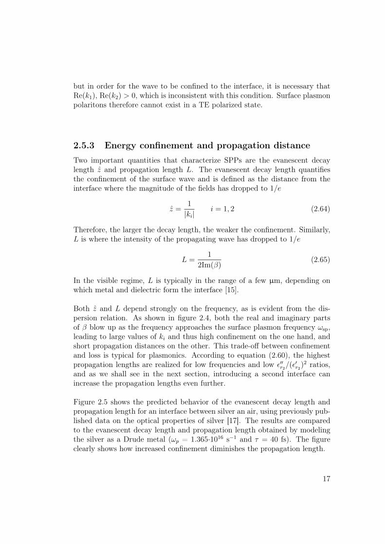
Figure 2.5 shows the predicted behavior of the evanescent decay length andpropagation length for an interface between silver an air, using previously pub-lished data on the optical properties of silver [17]. The results are comparedto the evanescent decay length and propagation length obtained by modelingthe silver as a Drude metal (ωp = 1.365·1016 s−1 and τ = 40 fs). The figureclearly shows how increased confinement diminishes the propagation length.
17
4 0 0 6 0 0 8 0 0 1 0 0 0 1 2 0 0 1 4 0 0 1 6 0 00 , 0
0 , 5
1 , 0
1 , 5
2 , 0
2 , 5
3 , 0 F r o m m e a s u r e d d a t a D r u d e m o d e l
�
���
����
����
������
��
�����
�
W a v e l e n g t h [ n m ]4 0 0 6 0 0 8 0 0 1 0 0 0 1 2 0 0 1 4 0 0 1 6 0 00
2 0 0
4 0 0
6 0 0
8 0 0
1 0 0 0
1 2 0 0 F r o m m e a s u r e d d a t a D r u d e m o d e l
�
�� ��
���
����
����L�
����
W a v e l e n g t h [ n m ]
Figure 2.5: The calculated evanescent decay length and propagation length foran interface between silver and air. Increasing the wavelength decreases theconfinement of the SPP mode while simultaneously allowing it to propagatefurther. The evanescent decay length calculated for the measured data is inparticularly good agreement with the results obtained from the Drude model.
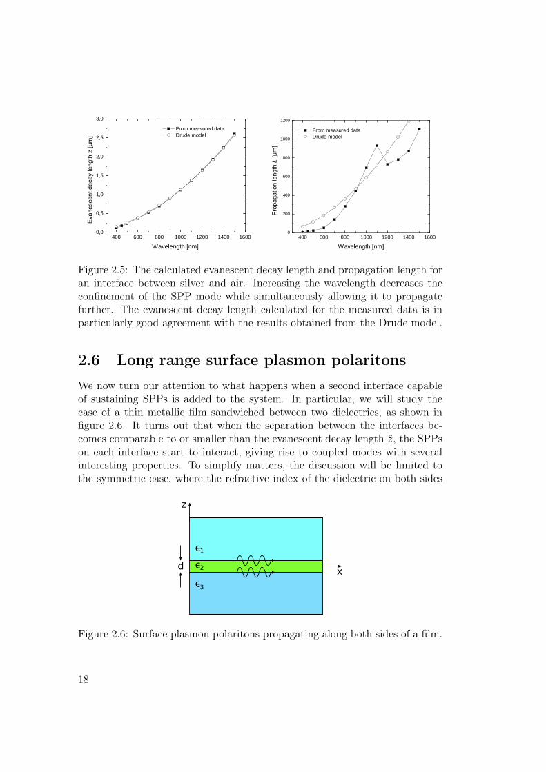
2.6 Long range surface plasmon polaritonsWe now turn our attention to what happens when a second interface capableof sustaining SPPs is added to the system. In particular, we will study thecase of a thin metallic film sandwiched between two dielectrics, as shown infigure 2.6. It turns out that when the separation between the interfaces be-comes comparable to or smaller than the evanescent decay length z, the SPPson each interface start to interact, giving rise to coupled modes with severalinteresting properties. To simplify matters, the discussion will be limited tothe symmetric case, where the refractive index of the dielectric on both sides
ϵ
ϵ
1
3
z
xϵ2d
Figure 2.6: Surface plasmon polaritons propagating along both sides of a film.
18
of the film is the same, εr1 = εr3 .
In the previous analysis of a single interface it was shown that surface plas-mons can only exist in the TM polarized state. The governing equations werefound to be (repeated for convenience)
Ex = −i1
ωµε
∂By
∂z(2.45)
Ez = −β
ωµεBy (2.46)
∂2By
∂z2+(ω2µε− β2
)By = 0 (2.47)
As before, in the regions above and below the film, the TM wave equation(2.47) has solutions that decay exponentially away from the interfaces
By =
{Ae−k1(z−d/2)eiβx z > d/2
Bek1(z+d/2)eiβx z < −d/2
where k21 = β2 − ω2µ1ε1 (2.66)
However, in the film region −d/2 < z < d/2 the modes localized at eachinterface couple, yielding
By = Cek2(z−d/2)eiβx +De−k2(z+d/2)eiβx
where k22 = β2 − ω2µ2ε2 (2.67)
Now, with the help of equations (2.45) and (2.46), the remaining field compo-nents Ex and Ez can be calculated to give the following set of equations. Sinceall the field components have the spatial dependence on x, the propagationfactor eiβx has been omitted for the sake of clarity.
19
By = Ae−k1(z−d/2)
Ex = iAk1
ωµ1ε1e−k1(z−d/2)
Ez = −A β
ωµ1ε1e−k1(z−d/2)
z > d/2
By = Cek2(z−d/2) +De−k2(z+d/2)
Ex = − i
ωµ2ε2
(Ck2e
k2(z−d/2) −Dk2e−k2(z+d/2)
)Ez = − β
ωµ2ε2
(Cek2(z−d/2) +De−k2(z+d/2)
)
−d/2 < z < d/2
By = Bek1(z+d/2)
Ex = −iB k1
ωµ1ε1ek1(z+d/2)
Ez = −B β
ωµ1ε1ek1(z+d/2)
z < −d/2
For non-magnetic media (µ1 = µ2 = µ0), the tangential components of the Eand B fields must be continuous at the interfaces. Applying these boundaryconditions at z = ±d/2 leads to the following set of linear equations
z = +d/2 : A = C +De−k2d
k1
ε1A = −k2
ε2C +
k2
ε2De−k2d
z = −d/2 : B = Ce−k2d +D
k1
ε1B =
k1
ε1Ce−k2d − k2
ε2D
which can be more clearly expressed in matrix form∣∣∣∣∣∣∣∣1 0 −1 e−k2d
0 1 −e−k2d −1k1ε1
0 k2ε2
−k2ε2e−k2d
0 k1ε1−k2ε2e−k2d k2
ε2
∣∣∣∣∣∣∣∣∣∣∣∣∣∣∣∣ABCD
∣∣∣∣∣∣∣∣ = 0 (2.68)
20
This is a matrix equation of the form Mb = 0. In order for it to have a non-trivial solution, the determinant det(M) must be zero (otherwise M would beinvertible and b = M−10 = 0). Setting the determinant to zero gives thefollowing condition
e−k2d = ±k1/ε1 + k2/ε2k1/ε1 − k2/ε2
(2.69)
which implicitly links the propagation constant β and frequency ω via k1 andk2. In other words, it is the dispersion relation for the coupled SPP mode.Note that if d → ∞ we recover the condition for the existence of a surfaceplasmon polariton on a single interface (2.57).
If the negative solution of equation (2.69) is inserted into the matrix equation(2.68), it can be solved for the constants A through D. After some algebra wearrive at the following solution for the magnetic field component By. Here theconstant A has been normalized to A = 1.
By =
e−k1(z−d/2)eiβx z > d/2
−√
(k2/ε2)2−(k1/ε1)2
k2/ε2eiβx cosh(k2z) −d/2 < z < d/2
ek1(z+d/2)eiβx z < −d/2
(2.70)
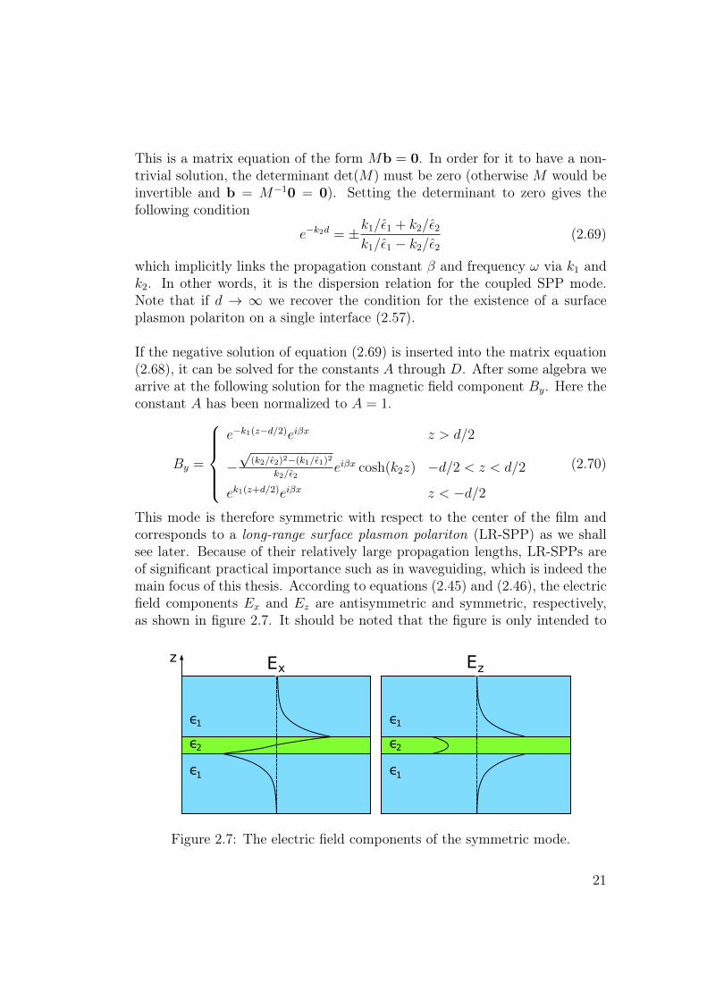
This mode is therefore symmetric with respect to the center of the film andcorresponds to a long-range surface plasmon polariton (LR-SPP) as we shallsee later. Because of their relatively large propagation lengths, LR-SPPs areof significant practical importance such as in waveguiding, which is indeed themain focus of this thesis. According to equations (2.45) and (2.46), the electricfield components Ex and Ez are antisymmetric and symmetric, respectively,as shown in figure 2.7. It should be noted that the figure is only intended to
ϵ
ϵ
1
1
z
xϵ2
ϵ
ϵ
1
1
ϵ2
Ex Ez
Figure 2.7: The electric field components of the symmetric mode.
21
give the reader a feel for the shape of the fields and are therefore not to scale.However, from equations (2.45) and (2.46) it can be seen that in the dielectric|Ez/Ex| = β/k1, and since β is always greater than k1 (see equation (2.66)),Ez is the dominant component.
Let us now investigate the mode that arises from the positive solution of equa-tion (2.69). Solving equation (2.68) and setting A = 1 as before, produces
By =
e−k1(z−d/2)eiβx z > d/2
−√
(k1/ε1)2−(k2/ε2)2
k2/ε2eiβx sinh(k2z) −d/2 < z < d/2
−ek1(z+d/2)eiβx z < −d/2
(2.71)
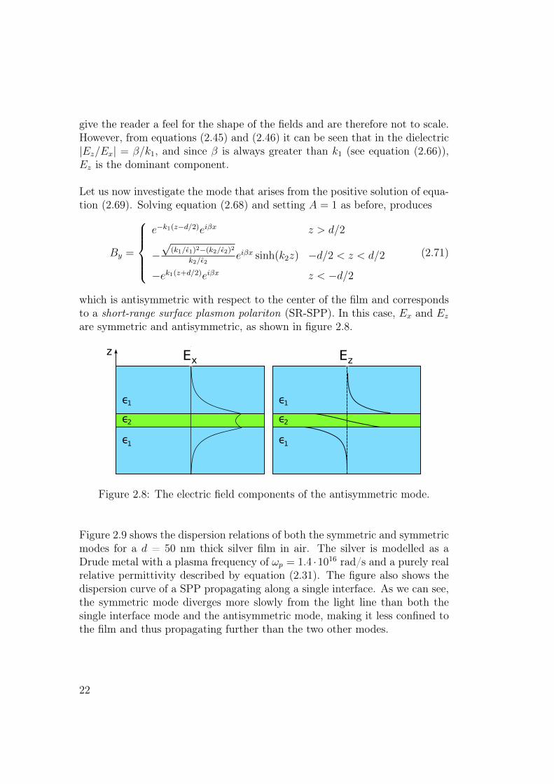
which is antisymmetric with respect to the center of the film and correspondsto a short-range surface plasmon polariton (SR-SPP). In this case, Ex and Ezare symmetric and antisymmetric, as shown in figure 2.8.
ϵ
ϵ
1
1
z
ϵ2
ϵ
ϵ
1
1
ϵ2
Ex Ez
Figure 2.8: The electric field components of the antisymmetric mode.
Figure 2.9 shows the dispersion relations of both the symmetric and symmetricmodes for a d = 50 nm thick silver film in air. The silver is modelled as aDrude metal with a plasma frequency of ωp = 1.4 ·1016 rad/s and a purely realrelative permittivity described by equation (2.31). The figure also shows thedispersion curve of a SPP propagating along a single interface. As we can see,the symmetric mode diverges more slowly from the light line than both thesingle interface mode and the antisymmetric mode, making it less confined tothe film and thus propagating further than the two other modes.
22
0 2 4 6 8 1 0 1 2 1 40
2
4
6
8
1 0
1 2
P r o p a g a t i o n c o n s t a n t � [ 1 0 7 m - 1 ]
Frequ
ency
� [10
15 s-1 ]
S y m m e t r i c m o d e A n t i s y m m e t r i c m o d e S P P d i s p e r s i o n
Figure 2.9: The dispersion relation of the symmetric and antisymmetric modesfor a 50 nm thick silver film in air. The dispersion relation of a single interfaceis also shown.
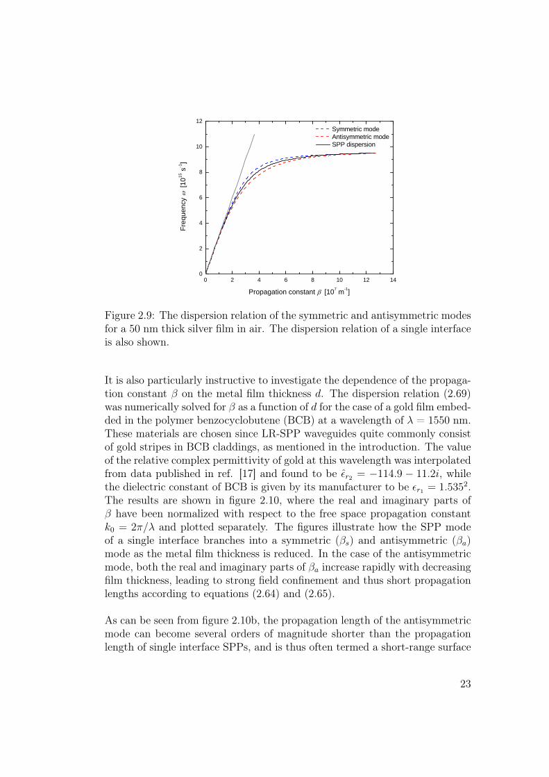
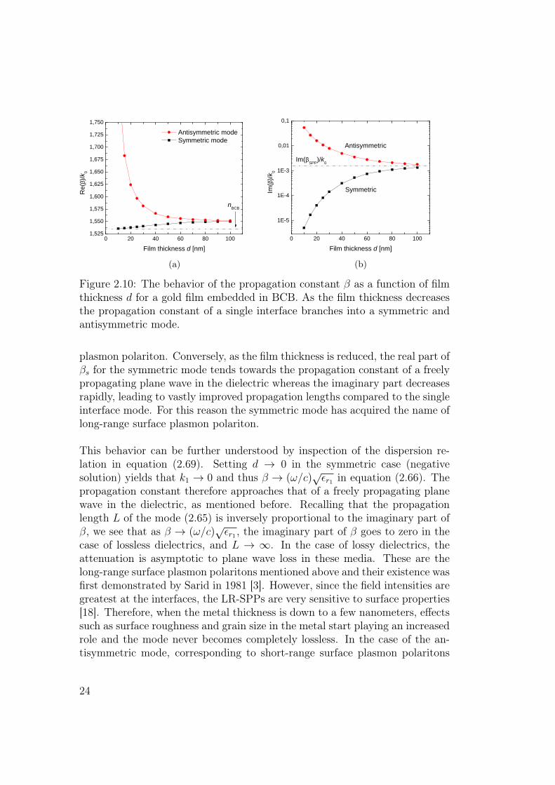
It is also particularly instructive to investigate the dependence of the propaga-tion constant β on the metal film thickness d. The dispersion relation (2.69)was numerically solved for β as a function of d for the case of a gold film embed-ded in the polymer benzocyclobutene (BCB) at a wavelength of λ = 1550 nm.These materials are chosen since LR-SPP waveguides quite commonly consistof gold stripes in BCB claddings, as mentioned in the introduction. The valueof the relative complex permittivity of gold at this wavelength was interpolatedfrom data published in ref. [17] and found to be εr2 = −114.9 − 11.2i, whilethe dielectric constant of BCB is given by its manufacturer to be εr1 = 1.5352.The results are shown in figure 2.10, where the real and imaginary parts ofβ have been normalized with respect to the free space propagation constantk0 = 2π/λ and plotted separately. The figures illustrate how the SPP modeof a single interface branches into a symmetric (βs) and antisymmetric (βa)mode as the metal film thickness is reduced. In the case of the antisymmetricmode, both the real and imaginary parts of βa increase rapidly with decreasingfilm thickness, leading to strong field confinement and thus short propagationlengths according to equations (2.64) and (2.65).
As can be seen from figure 2.10b, the propagation length of the antisymmetricmode can become several orders of magnitude shorter than the propagationlength of single interface SPPs, and is thus often termed a short-range surface
23
0 2 0 4 0 6 0 8 0 1 0 01 , 5 2 51 , 5 5 01 , 5 7 51 , 6 0 01 , 6 2 51 , 6 5 01 , 6 7 51 , 7 0 01 , 7 2 51 , 7 5 0
A n t i s y m m e t r i c m o d e S y m m e t r i c m o d e
Re(β)
/k 0
F i l m t h i c k n e s s d [ n m ]
n B C B
0 2 0 4 0 6 0 8 0 1 0 0
1 E - 5
1 E - 4
1 E - 3
0 , 0 1
0 , 1
Im(β)
/k 0
F i l m t h i c k n e s s d [ n m ]
A n t i s y m m e t r i c
S y m m e t r i c
I m ( β S P P ) / k 0
(a) (b)
Figure 2.10: The behavior of the propagation constant β as a function of filmthickness d for a gold film embedded in BCB. As the film thickness decreasesthe propagation constant of a single interface branches into a symmetric andantisymmetric mode.
plasmon polariton. Conversely, as the film thickness is reduced, the real part ofβs for the symmetric mode tends towards the propagation constant of a freelypropagating plane wave in the dielectric whereas the imaginary part decreasesrapidly, leading to vastly improved propagation lengths compared to the singleinterface mode. For this reason the symmetric mode has acquired the name oflong-range surface plasmon polariton.
This behavior can be further understood by inspection of the dispersion re-lation in equation (2.69). Setting d → 0 in the symmetric case (negativesolution) yields that k1 → 0 and thus β → (ω/c)
√εr1 in equation (2.66). The
propagation constant therefore approaches that of a freely propagating planewave in the dielectric, as mentioned before. Recalling that the propagationlength L of the mode (2.65) is inversely proportional to the imaginary part ofβ, we see that as β → (ω/c)
√εr1 , the imaginary part of β goes to zero in the
case of lossless dielectrics, and L → ∞. In the case of lossy dielectrics, theattenuation is asymptotic to plane wave loss in these media. These are thelong-range surface plasmon polaritons mentioned above and their existence wasfirst demonstrated by Sarid in 1981 [3]. However, since the field intensities aregreatest at the interfaces, the LR-SPPs are very sensitive to surface properties[18]. Therefore, when the metal thickness is down to a few nanometers, effectssuch as surface roughness and grain size in the metal start playing an increasedrole and the mode never becomes completely lossless. In the case of the an-tisymmetric mode, corresponding to short-range surface plasmon polaritons
24
(positive solution), when d → 0, then k2 → 0 and therefore β → (ω/c)√εr2 ,
which is the propagation constant of a wave propagating through the metal.As discussed in section 2.3, most metals are opaque at visible and higher wave-lengths and the SR-SPPs are therefore very quickly attenuated.
An equivalent way of looking at this is to consider the confinement. In theantisymmetric case, as d → 0 then β → (ω/c)
√εr2 as before, which leads
to k1 → (ω/c)√εr2 − εr1 6= 0 in equation (2.66). In the symmetric case
β → (ω/c)√εr1 as d → 0, which means that k1 → 0. Since k1 quantifies
the confinement of the mode, the field is obviously more confined in the anti-symmetric mode and thus more energy is carried and dissipated by the lossymetal than in the symmetric case, where the dissipation from the metal isreduced.
In addition to LR-SPPs having a significantly longer propagation length thantheir single interface counterparts, they don’t have to be excited via incon-venient means such as gratings or prisms. Instead, due to their symmetry,LR-SPPs can be excited efficiently by end-fire coupling (a well known tech-nique in integrated optics) by matching an incident light field to the LR-SPPmode [4].
So far, we have only considered the case where the permittivity ε varies inone spatial coordinate, ε = ε(z), in particular an infinitely wide metal filmsandwiched between identical dielectric layers. Such configurations are of lim-ited practical interest since a propagating wave will spread out laterally awayfrom its source due to the confinement only being along the vertical axis.In the year 2000, Berini was the first to theoretically demonstrate that metalfilms of finite width were capable of guiding LR-SPPs, offering two-dimensionalconfinement to the modes [5]. Although these metal stripes have a relativelysimple geometry, their modes cannot be determined by analytical means andnumerical techniques such as the method of lines (used by Berini) and thefinite element method must be used instead. Berini also showed that the fielddistribution along the stripe waveguide width can resemble a Gaussian fieldclosely enough that LR-SPPs can be efficiently excited with end-fire excita-tion. This was realized experimentally shortly thereafter on a 8 µm wide, 20nm thick and 3.5 mm long gold stripe embedded in SiO2 using a polarizationmaintaining optical fiber at λ = 1550 nm [6].
25

26
3 Modeling
This section explains how the finite element method was used with the helpof the software suite COMSOL MultiphysicsTM to model the behavior of LR-SPP waveguides and devices. The chapter starts with an introduction to thefinite element method and COMSOL, and is followed by a look at the relevantpartial differential equations and the corresponding boundary conditions. Thedifferent types of meshes available in COMSOL are discussed, as well as howthey can be manually defined in order to mesh thin stripe waveguides. Thechapter concludes by explaining how the the various aspects of the finite ele-ment methods and material properties were tied together to produce realisticmodels of resistively heated LR-SPP waveguides.
Although most of the modeling was done in COMSOL, for the most partthe discussion keeps clear of aspects that are specific to COMSOL and insteadfocuses on the parts of the modeling that all modern finite element softwarehave in common.
3.1 The finite element method and COMSOLThe finite element method (FEM) is a numerical technique for finding ap-proximate solutions to problems that can be described by partial differentialequations (PDEs) or the minimization of a functional. It first originated as amethod for analyzing stress in civil engineering, but has since then found itsway into a number of different scientific disciplines where it has become a keytechnology in the modeling of advanced engineering and scientific problems,such as heat transfer, fluid flow, electric and magnetic fields and many others.The versatility of the method, along with the fact that it can be applied toproblems involving complex geometries and boundaries with relative ease, hasmade it particularly popular in academic and commercial circles.
The basic idea behind the finite element method is to partition, or discretize,the geometry into smaller pieces called finite elements. Each element is of asimple geometry and thus much easier to analyze than the actual structure.The elements are connected to each other at their corners, known as vertices,and together they form a mesh of the actual structure. Within each of theelements, the unknown field quantity being sought φ (e.g. the temperature orelectric field) is approximated with the use of simple smooth functions such
27
as polynomials, known as interpolation or shape functions. The field quantitycan then be expressed as [22]
φ = N1φ1 +N2φ2 + · · ·+Nmφm
where the Ni are the interpolation functions and the φi are the values of theunknown field at the element vertices. Finite elements with linear interpolationfunctions produce exact values for φi if the solution being sought is quadratic,quadratic elements give exact values for φi for cubic solutions, etc [23]. Thesolutions are however in general not exact and the accuracy can depend highlyon the number of elements used. A finer mesh will normally yield more ac-curate results but at a greater computational cost. For this reason the meshis normally not uniform over the entire structure, but rather finer in regionswhere the rate of change of the field is great or where the precision of the resultis critical to the analysis.
By applying the appropriate laws or principles, depending on the particu-lar problem, a matrix equation governing the behavior of each element canbe obtained. This resulting element characteristic matrix has different namesdepending on the particular field of study: in solid mechanics it is called thestiffness matrix and in heat conduction it is called the conductivity matrix.There are several ways of deriving the element characteristic matrix, the mostimportant being the variational method and the weighted residual method.
The variational method is applicable to problems that can be stated as theminimization of a functional, such as a functional describing the total energyof the system (cf. Hamilton’s principle). The variational approach can beused as long as a variational principle corresponding to the problem of interestexists, but this is not always the case. The weighted residual methods areparticularly suited for problems for which differential equations are known butno variational statement is available [24]. They are based on the minimizationof the residual left after an approximate or trial solution is substituted intothe differential equations governing the problem [22], and are general mathe-matical tools applicable, in principle, for solving all kinds of partial differentialequations [25]. The most popular variational method is the so-called Galerkinmethod [24].
Once all the element characteristic matrices have been established, they areassembled into a global set of linear simultaneous equations for the entire prob-lem domain, which can be easily solved to obtain the required field quantity atthe vertices, φi. The assembly is performed by adding up all the contributions
28
to a mesh vertex from each of the elements that share it. Before the globalsystem of equations is solved, it must be modified in order to take the bound-ary and initial conditions into account.
The global system of equations typically involves a sparse and symmetric ma-trix and the problem can thus be efficiently solved with methods designed tohandle such matrices, much more efficiently than say, by inverting it. There aretwo main types of methods for solving simultaneous equations: direct meth-ods and iterative methods [25]. Direct methods include the well known Gausselimination and LU decomposition methods and require that the system ofequations is fully assembled before they are initiated. They can therefore re-quire significant storage space, especially for problems involving a great numberof mesh vertices. Iterative methods, such as the Gauss-Deidel method, tendto work better for larger systems since they can be coded in a way that avoidsthe full assembly of the system matrix [25].
The final step of a finite element simulation usually involves calculating allthe secondary quantities of the problem, such as the conductive heat flux inthe simulation of heat transfer, or the time-averaged power flow in the analy-sis of electric fields. In recent years, many commercial software products havebecome available that attempt to automate finite element simulations as muchas possible, such as COMSOL Multiphysics [26].
COMSOL Multiphysics (previously known as FEMlab) is an interactive en-vironment for modeling and solving scientific and engineering problems basedon PDEs. It provides sophisticated tools for geometric modeling and a largematerials database. It does not require a deep understanding of PDEs or nu-merical analysis but instead gives users access to the relevant variables throughintuitive interfaces. COMSOL lets users define their own PDEs in the coeffi-cient form, general form or in the weak form. It also provides several modulesthat are useful to various different fields, such as the acoustics module, theheat transfer module, RF module, chemical engineering module and manymore. Through the Multiphysics feature, the differential equations from eachof these modules can be coupled together to better describe realistic physi-cal phenomena. Since the work presented in this thesis is concerned with theoptical modes of stripe and nanowire waveguides and how waveguides can beheated to realize active devices, the simulations only make use of the heattransfer module and the RF module, and the following discussion is thereforelimited to them.
29
The first step in creating any model in COMSOL is to define the geometry ofthe system with the use of a set of traditional computer aided design (CAD)tools. Next, the necessary material information such as the refractive index orthermal conductivity is provided and COMSOL provides a substantial materialdatabase to aid in this regard. COMSOL not only allows for the input of fixedmaterial constants but also for expressions that can depend on one or more ofthe model’s dependent variables. After the appropriate boundary conditionshave been applied, the structure is discretized with one of the several meshingalgorithms available and the relevant differential equation then solved.
3.2 PDEs and boundary conditionsWhen investigating the optical modes of metal waveguides and how they canbe affected by heating, the relevant partial differential equations that must besolved are of course the heat transfer equation and Maxwell’s equations. Eachof these equations is associated with a set of boundary conditions.
3.2.1 Heat transfer
In order to calculate the temperature profile of a heated waveguide structure,COMSOL solves the following form of the heat transfer equation [27]
ρCp∂T
∂t+∇ · (−k∇T ) = Q− ρCpu · ∇T (3.1)
where ρ is the density, Cp is the specific heat capacity at constant pressure,T is the absolute temperature, k is the thermal conductivity, Q is the powerdensity of heat source and u is the velocity field vector of the material (onlynon-zero for fluids). At the boundaries of each subdomain, COMSOL offers achoice between the following boundary conditions: heat flux, thermal insula-tion, convective flux and fixed temperature.
The heat flux condition is a mixed boundary condition that not only accountsfor general heat flux but also for transfer of heat due to convection and radia-tion:
n · (k∇T ) = q0 + h (Tinf − T ) + σε(T 4
amb − T 4)
(3.2)
where n is a normal vector to the boundary, q0 represents the inward heatflux normal to the boundary from an external source, h is the heat transfercoefficient, Tinf is the external bulk temperature, σ is the Stefan-Boltzmannconstant, ε the surface emissivity of the object and Tamb is ambient tempera-
30
ture.
The thermal insulation boundary condition is a special case of the heat fluxcondition where all the heat transfer mechanisms across the boundary havebeen disabled [27]
n · (k∇T ) = 0 (3.3)
This equation tells us that the normal component of the temperature gradientis zero, which means that there is no transfer of heat across it and the boundaryis therefore insulating. The convective flux boundary condition is also a specialcase of the general heat flux condition, in which all the heat that passes througha boundary does so by means of convection:
n · (k∇T ) = 0 where n · q = ρCpuT (3.4)
where q is the heat flux vector. Last but not least is the fixed temperatureboundary condition which, as the name suggests, simply fixes the temperatureof a boundary to a given temperature T0
T = T0 (3.5)
3.2.2 Eigenmode analysis
The ’perpendicular waves’ application mode in COMSOL is a 2D eigenmodesolver which calculates the mode field F (x, y) of a wave propagating in thez direction. It belongs to the RF module and solves the following version ofMaxwell’s curl equations for non-magnetic materials
∇×∇× E− n2(x, y)k20E = 0 (3.6)
∇× n−2(x, y)∇×H− k20H = 0 (3.7)
where H = H (x, y) ei(βz−ωt), E = E (x, y) ei(βz−ωt), k20 = ω2µ0ε0 and β is the
propagation constant in the z direction. In addition to the boundary conditionsthat always have to be satisfied in electromagnetic theory (such as the tangen-tial component of the E and H fields being continuous across an interface, etc),COMSOL’s RF module provides several additional types of boundary condi-tions designed to simplify the modeling process. These include conditions thatallow the boundaries to behave as perfect electric or magnetic conductors (i.e.n×E = 0, or n×H = 0), and the perfectly matched layer (PML) condition. APML is strictly speaking not a boundary condition but an additional domainthat absorbs the incident radiation without producing reflections [27]. Two
31
further conditions are the scattering and impedance boundary conditions, andare closely related to the PML condition. The most commonly used boundaryconditions in the work presented here are the perfect electrical conductor andPML conditions.
3.3 MeshingThe most delicate aspect of the simulation process is arguably the meshing ofthe structure. As explained before, it is not the geometry of the structure itselfthat gets used in the solution of the PDEs but rather the discretization, or themesh, of the structure. A good mesh must strike a balance between being fineenough to resolve all the important aspects of the solution in enough detail,but still not consist of so many vertices that the computer’s resources runout during the simulation process. Most finite element analysis software suitssuch as COMSOL provide automatic meshers which usually do a very goodjob. But because of the extreme aspect ratio of plasmonic stripe waveguides(several nm in thickness versus several µm in width) the automatic meshersare in many cases not sufficient since they often neglect to create mesh verticesinside the stripes. The user must therefore have some degree of control overhow the mesh is generated. Furthermore, the mesh must reflect the fact thatLR-SPP modes typically extend several µm into the cladding away from themetal waveguides. The most common types of meshes are the free mesh andmapped mesh, which consist of triangular and quadrilateral elements in twodimensional structures, respectively, and tetrahedral and hexahedral elementsin three dimensions.
The free mesh is based on the Delauney algorithm which is a triangulationmethod valid for any number of dimensions [28]. The main strength of thismethod is that it can be used for all types of geometries, regardless of theirshape or topology. In COMSOL, the user can influence the mesh through aset of adjustable parameters, such as by specifying the maximum element sizeand the element growth rate (i.e. how fast the element size may grow from anarea with small elements to an area with larger ones).
The mapped mesh is substantially more limited than the free mesh and canonly be used to mesh geometries that are fairly regular and rectangular. Itfurthermore requires that the subdomains of the geometry are free of isolatedvertices and boundary segments and that they are bounded by at least fourboundary segments. However, if some of these requirements are not met,the geometry can often be altered slightly in order to successfully mesh it.
32
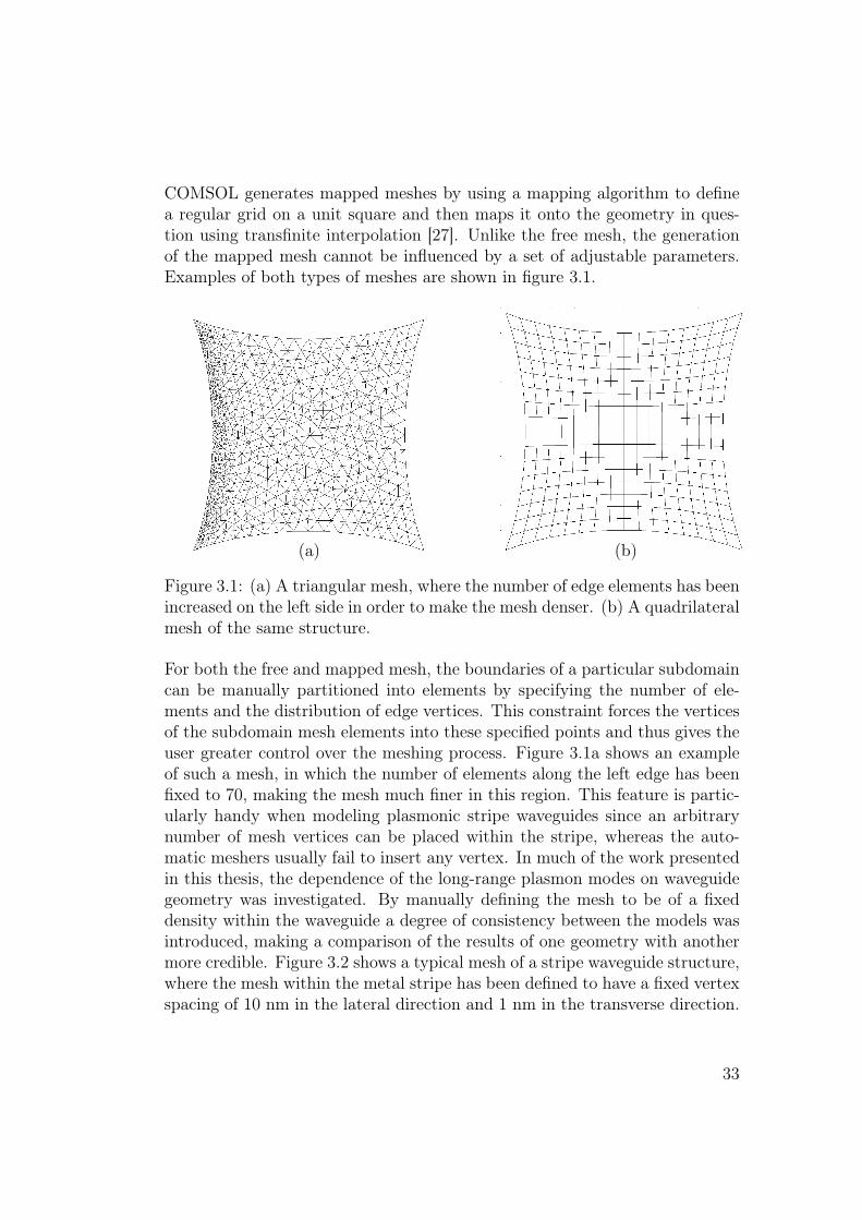
COMSOL generates mapped meshes by using a mapping algorithm to definea regular grid on a unit square and then maps it onto the geometry in ques-tion using transfinite interpolation [27]. Unlike the free mesh, the generationof the mapped mesh cannot be influenced by a set of adjustable parameters.Examples of both types of meshes are shown in figure 3.1.
(a) (b)
Figure 3.1: (a) A triangular mesh, where the number of edge elements has beenincreased on the left side in order to make the mesh denser. (b) A quadrilateralmesh of the same structure.
For both the free and mapped mesh, the boundaries of a particular subdomaincan be manually partitioned into elements by specifying the number of ele-ments and the distribution of edge vertices. This constraint forces the verticesof the subdomain mesh elements into these specified points and thus gives theuser greater control over the meshing process. Figure 3.1a shows an exampleof such a mesh, in which the number of elements along the left edge has beenfixed to 70, making the mesh much finer in this region. This feature is partic-ularly handy when modeling plasmonic stripe waveguides since an arbitrarynumber of mesh vertices can be placed within the stripe, whereas the auto-matic meshers usually fail to insert any vertex. In much of the work presentedin this thesis, the dependence of the long-range plasmon modes on waveguidegeometry was investigated. By manually defining the mesh to be of a fixeddensity within the waveguide a degree of consistency between the models wasintroduced, making a comparison of the results of one geometry with anothermore credible. Figure 3.2 shows a typical mesh of a stripe waveguide structure,where the mesh within the metal stripe has been defined to have a fixed vertexspacing of 10 nm in the lateral direction and 1 nm in the transverse direction.
33
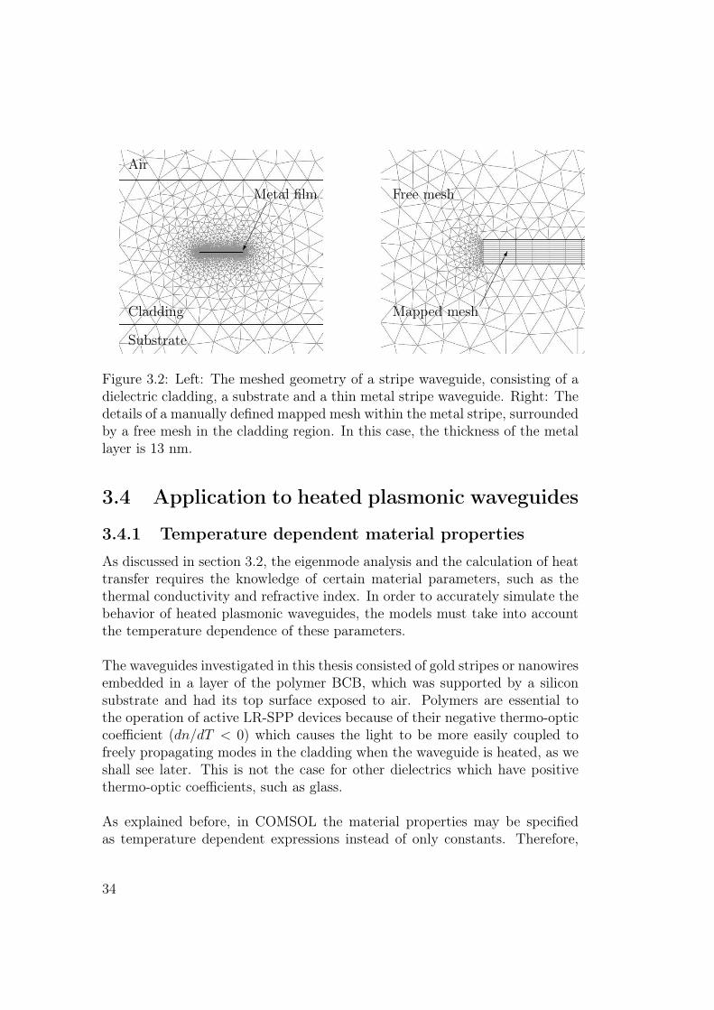
Air
Cladding
Substrate
Metal film
Mapped mesh
Free mesh�����
������
Figure 3.2: Left: The meshed geometry of a stripe waveguide, consisting of adielectric cladding, a substrate and a thin metal stripe waveguide. Right: Thedetails of a manually defined mapped mesh within the metal stripe, surroundedby a free mesh in the cladding region. In this case, the thickness of the metallayer is 13 nm.
3.4 Application to heated plasmonic waveguides
3.4.1 Temperature dependent material properties
As discussed in section 3.2, the eigenmode analysis and the calculation of heattransfer requires the knowledge of certain material parameters, such as thethermal conductivity and refractive index. In order to accurately simulate thebehavior of heated plasmonic waveguides, the models must take into accountthe temperature dependence of these parameters.
The waveguides investigated in this thesis consisted of gold stripes or nanowiresembedded in a layer of the polymer BCB, which was supported by a siliconsubstrate and had its top surface exposed to air. Polymers are essential tothe operation of active LR-SPP devices because of their negative thermo-opticcoefficient (dn/dT < 0) which causes the light to be more easily coupled tofreely propagating modes in the cladding when the waveguide is heated, as weshall see later. This is not the case for other dielectrics which have positivethermo-optic coefficients, such as glass.
As explained before, in COMSOL the material properties may be specifiedas temperature dependent expressions instead of only constants. Therefore,
34
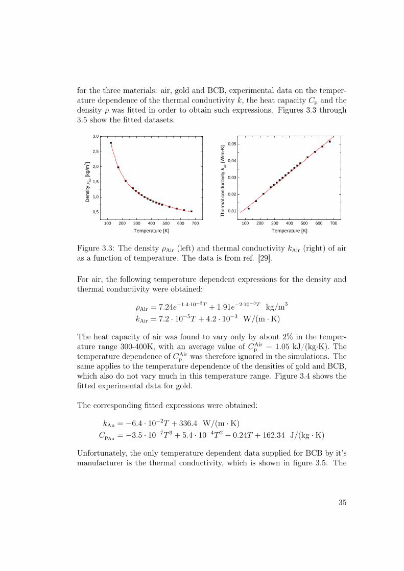
for the three materials: air, gold and BCB, experimental data on the temper-ature dependence of the thermal conductivity k, the heat capacity Cp and thedensity ρ was fitted in order to obtain such expressions. Figures 3.3 through3.5 show the fitted datasets.
1 0 0 2 0 0 3 0 0 4 0 0 5 0 0 6 0 0 7 0 0
0 , 5
1 , 0
1 , 5
2 , 0
2 , 5
3 , 0
Dens
ity � Air
[kg/m
3 ]
T e m p e r a t u r e [ K ]1 0 0 2 0 0 3 0 0 4 0 0 5 0 0 6 0 0 7 0 0
0 , 0 1
0 , 0 2
0 , 0 3
0 , 0 4
0 , 0 5
�
� ���
���
���
�������
k ������
�����
T e m p e r a t u r e [ K ]
Figure 3.3: The density ρAir (left) and thermal conductivity kAir (right) of airas a function of temperature. The data is from ref. [29].
For air, the following temperature dependent expressions for the density andthermal conductivity were obtained:
ρAir = 7.24e−1.4·10−2T + 1.91e−2·10−3T kg/m3
kAir = 7.2 · 10−5T + 4.2 · 10−3 W/(m ·K)
The heat capacity of air was found to vary only by about 2% in the temper-ature range 300-400K, with an average value of CAir
p = 1.05 kJ/(kg·K). Thetemperature dependence of CAir
p was therefore ignored in the simulations. Thesame applies to the temperature dependence of the densities of gold and BCB,which also do not vary much in this temperature range. Figure 3.4 shows thefitted experimental data for gold.
The corresponding fitted expressions were obtained:
kAu = −6.4 · 10−2T + 336.4 W/(m ·K)
CpAu= −3.5 · 10−7T 3 + 5.4 · 10−4T 2 − 0.24T + 162.34 J/(kg ·K)
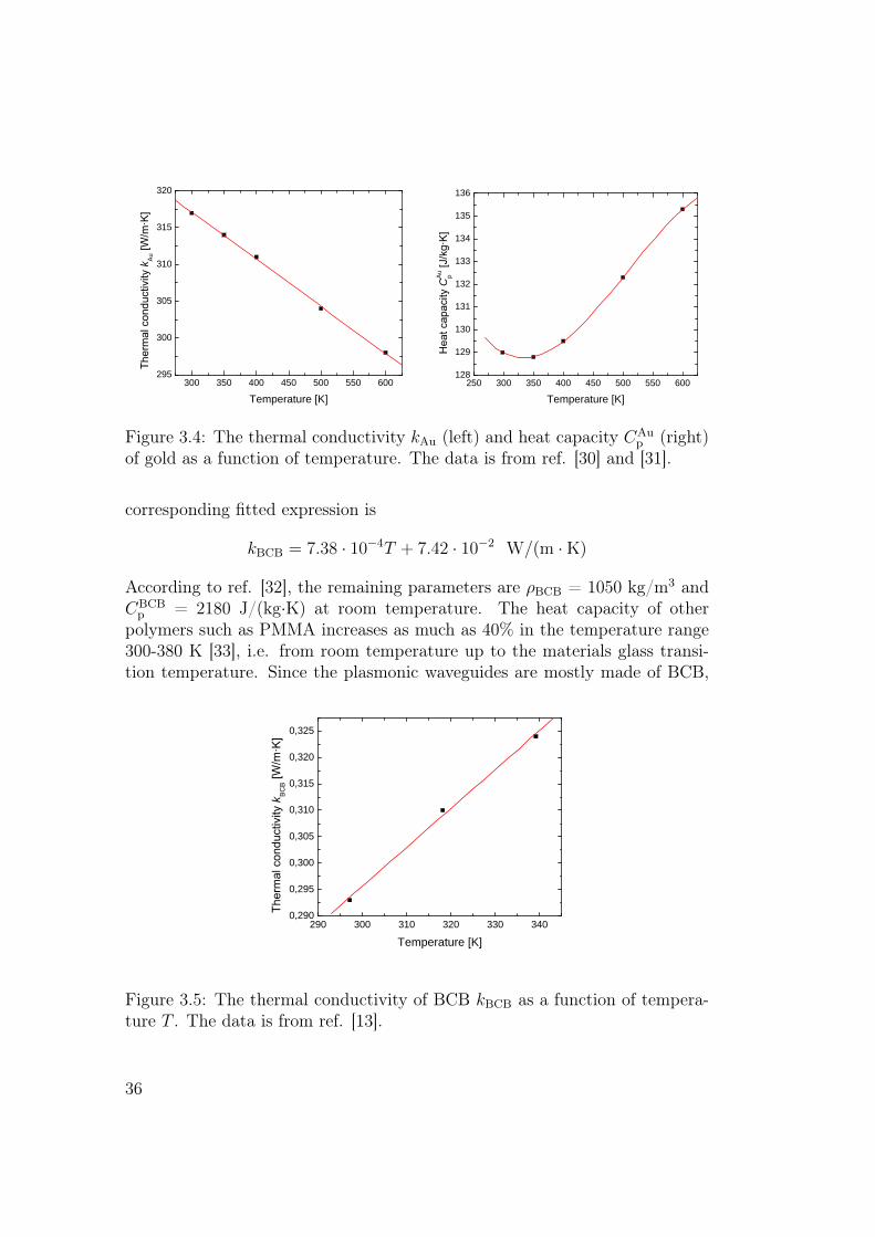
Unfortunately, the only temperature dependent data supplied for BCB by it’smanufacturer is the thermal conductivity, which is shown in figure 3.5. The
35
3 0 0 3 5 0 4 0 0 4 5 0 5 0 0 5 5 0 6 0 02 9 5
3 0 0
3 0 5
3 1 0
3 1 5
3 2 0
�
� ���
���
���
�������
k �����
�����
T e m p e r a t u r e [ K ]2 5 0 3 0 0 3 5 0 4 0 0 4 5 0 5 0 0 5 5 0 6 0 01 2 8
1 2 91 3 01 3 11 3 21 3 31 3 41 3 51 3 6
�
����
�
���C�� �
������
���
T e m p e r a t u r e [ K ]
Figure 3.4: The thermal conductivity kAu (left) and heat capacity CAup (right)
of gold as a function of temperature. The data is from ref. [30] and [31].
corresponding fitted expression is
kBCB = 7.38 · 10−4T + 7.42 · 10−2 W/(m ·K)
According to ref. [32], the remaining parameters are ρBCB = 1050 kg/m3 andCBCB
p = 2180 J/(kg·K) at room temperature. The heat capacity of otherpolymers such as PMMA increases as much as 40% in the temperature range300-380 K [33], i.e. from room temperature up to the materials glass transi-tion temperature. Since the plasmonic waveguides are mostly made of BCB,
2 9 0 3 0 0 3 1 0 3 2 0 3 3 0 3 4 00 , 2 9 0
0 , 2 9 5
0 , 3 0 0
0 , 3 0 5
0 , 3 1 0
0 , 3 1 5
0 , 3 2 0
0 , 3 2 5
�
�� ��
����
����
�������
k ������
����
T e m p e r a t u r e [ K ]
Figure 3.5: The thermal conductivity of BCB kBCB as a function of tempera-ture T . The data is from ref. [13].
36
a more accurate description of their heating would be obtained by relying onexperimentally observed data of the heat capacity versus temperature insteadjust of a constant value. Unfortunately, this is unavailable at present and themodels must make do without it.
The optical properties of the BCB and gold are also temperature dependent.The thermo-optic coefficient of BCB has previously been determined to bedn/dT ∼ −2.5 · 10−5 K−1 [34], and assuming that dn/dT is itself not temper-ature dependent, the relation between nBCB and T can be written as
nBCB(T ) = −2.5 · 10−5T + C (3.8)
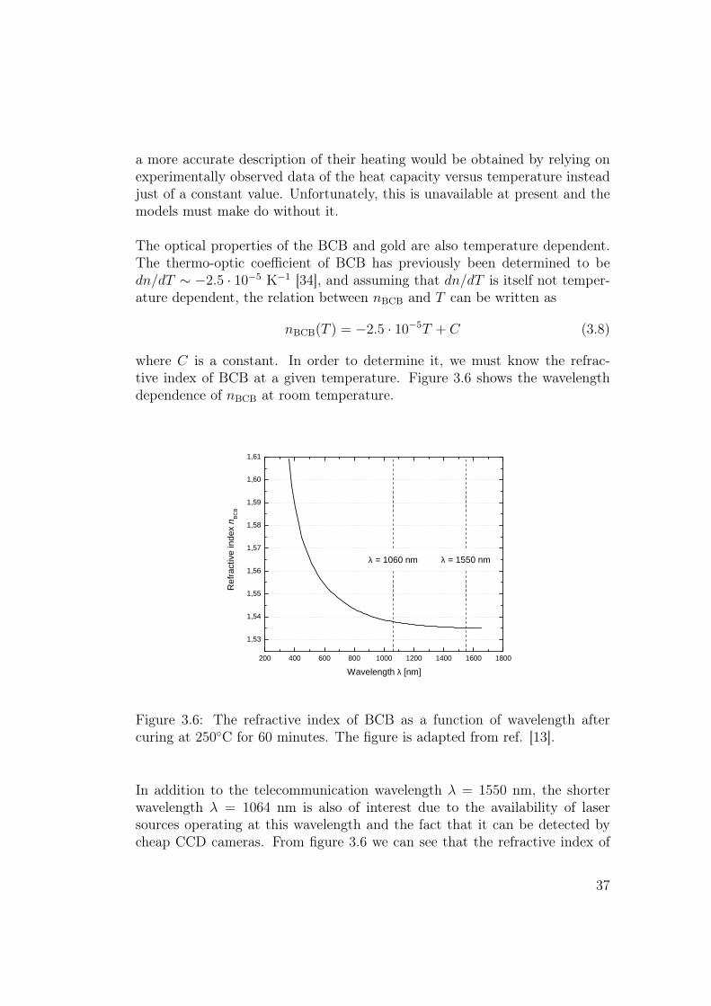
where C is a constant. In order to determine it, we must know the refrac-tive index of BCB at a given temperature. Figure 3.6 shows the wavelengthdependence of nBCB at room temperature.
2 0 0 4 0 0 6 0 0 8 0 0 1 0 0 0 1 2 0 0 1 4 0 0 1 6 0 0 1 8 0 0
1 , 5 3
1 , 5 4
1 , 5 5
1 , 5 6
1 , 5 7
1 , 5 8
1 , 5 9
1 , 6 0
1 , 6 1
λ = 1 5 5 0 n m
Refra
ctive i
ndex
n BCB
W a v e l e n g t h λ [ n m ]
λ = 1 0 6 0 n m
Figure 3.6: The refractive index of BCB as a function of wavelength aftercuring at 250◦C for 60 minutes. The figure is adapted from ref. [13].
In addition to the telecommunication wavelength λ = 1550 nm, the shorterwavelength λ = 1064 nm is also of interest due to the availability of lasersources operating at this wavelength and the fact that it can be detected bycheap CCD cameras. From figure 3.6 we can see that the refractive index of
37
BCB at room temperature is nBCB = 1.538 for λ = 1064 nm, and nBCB =1.535 for λ = 1550 nm, which leads us to the following temperature dependentexpression for nBCB
nBCB(T ) =
{−2.5 · 10−5T + 1.5425 for λ = 1550 nm−2.5 · 10−5T + 1.5455 for λ = 1064 nm
(3.9)
Similarly, the temperature dependent refractive index of gold nAu = n + iκmust be determined. According to ref. [35], the thermo-optic coefficients of nand κ are
dn/dt ≈ 3.5 · 10−4 K−1
dκ/dt ≈ −1.4 · 10−3 K−1 (3.10)
for λ = 1064 nm and
dn/dt ≈ 5 · 10−4 K−1
dκ/dt ≈ −1.7 · 10−3 K−1 (3.11)
for λ = 1550 nm. In the latter case, the thermo-optic coefficients have beenextrapolated to a wavelength of λ = 1550 nm since the data in ref. [35] onlygoes up to a wavelength of λ = 1240 nm. The complex refractive index of goldat room temperature at these wavelengths is (see figure 2.2)
nAu =
{0.26 + 6.96i for λ = 1064 nm0.52 + 10.73i for λ = 1550 nm
This, in addition to the thermo-optic coefficients leads us to the followingtemperature dependent refractive index of gold
nAu(T ) =
{(5 · 10−4T + 0.37) +i(−1.7 · 10−3T + 11.24) for λ = 1550nm(3.5 · 10−4T + 0.15) +i(−1.4 · 10−3T + 7.38) for λ = 1064nm
(3.12)
3.4.2 The modeling of heated waveguides
As explained before, the first step in any finite element simulation is to specifythe geometry of the structure being investigated. It is naturally neither possi-ble nor practical to perfectly replicate the structure of the subject, and certainsimplifications must therefore be made.
In simulating the plasmonic waveguides, the stripes or nanowires were po-sitioned in the direct center of the BCB cladding, which was 20 µm thick in
38
the case of stripe waveguides and anywhere between 20 and 40 µm in thecase of nanowires. Although the width of the BCB is in practice of the orderof millimeters, it was normally limited to ∼100 µm since the waveguide modeprofiles were found to vanish at around 20 µm away from the stripe. Initially, a10 µm thick silicon substrate beneath the BCB was also included in the modelsbut was found to have a negligible effect on the calculated modes and effectivemode indices. It was therefore eventually omitted to save on computing time.Last but not least, the entire structure was simulated as being enclosed by alayer of air which was thick enough so that at least one row of mesh verticeswas placed in the middle of the air layer when it was automatically meshed.
The resistive heating of the waveguide structure was introduced into the mod-els by setting the metal waveguides as heat sources of constant power. In orderto increase the accuracy of the simulations the temperature dependent thermalproperties and refractive index as determined in section 3.4.1 were used. Thesilicon substrate was assumed to act as an efficient heatsink at room tempera-ture and a fixed temperature boundary condition was therefore applied to thelower BCB boundary, as shown in figure 3.7. Because of the fixed temperatureboundary condition, the silicon substrate didn’t have any influence on the re-sulting temperature profile and the thermal properties of silicon were thereforenot needed. Furthermore, in many of the models the silicon was simply omit-ted, as noted before. The most natural way of modeling the effect of air atthe top BCB surface would have been to apply a general heat flux boundarycondition to the boundary. However, modeling with convective heat transfercan often be quite problematic because the heat transfer coefficient between airand many materials, such as BCB, is not known. Furthermore, some assump-tions about the velocity field of the air have to made which are hard to justifywithout having made detailed investigations on the flow of air around such asmall structure. The loss of heat to the surroundings were therefore insteadmodelled by setting the temperature distribution to be continuous across theBCB boundary1 and setting the outer boundaries of the air box to be fixed atroom temperature. The continuity boundary condition effectively treats theair as being still, but still being able to remove heat from the structure.
Once the models had been set up in this manner, the temperature profileswere calculated using equation (3.1). Figure 3.7 shows an example of suchtemperature profiles, although it should be borne in mind that not all of theenclosing air is shown.
1This arises naturally in finite element simulations due to the continuity of the finiteelement field.
39
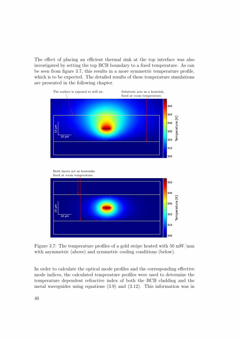
The effect of placing an efficient thermal sink at the top interface was alsoinvestigated by setting the top BCB boundary to a fixed temperature. As canbe seen from figure 3.7, this results in a more symmetric temperature profile,which is to be expected. The detailed results of these temperature simulationsare presented in the following chapter.
The surface is exposed to still air.
BBBBBBN
Substrate acts as a heatsink,fixed at room temperature.
?
Both layers act as heatsinksfixed at room temperature.
?
?
Figure 3.7: The temperature profiles of a gold stripe heated with 50 mW/mmwith asymmetric (above) and symmetric cooling conditions (below).
In order to calculate the optical mode profiles and the corresponding effectivemode indices, the calculated temperature profiles were used to determine thetemperature dependent refractive index of both the BCB cladding and themetal waveguides using equations (3.9) and (3.12). This information was in
40
turn used to calculate the optical mode profiles and the effective mode indicesvia equations (3.6) and (3.7). COMSOL handles all the natural boundary con-ditions of the electric and magnetic fields automatically, but additionally theouter boundary of the air box was set to behave as a perfect electric conductor.In principle, the type of boundary condition should not matter since the fieldwill be confined to within the BCB because of the surrounding air.
In addition to the LR-SPP modes supported by the stripes and nanowires,the cladding of a structure is also capable of sustaining a number of opticalmodes (known as cladding modes) due to its refractive index being higher thanthat of the surrounding air. Furthermore, a geometry can be found to sustaina number of different modes which are simply artifacts of the particular dis-cretization used, the selected cladding geometry and the solution process. Forthese reasons, COMSOL limits the number of modes it searches for and re-quires the user to enter a reasonable initial “guess” of the effective mode indexof the desired mode. Because the metal waveguides are so tiny compared to thecladding, the effective mode index of LR-SPP modes is usually only slightlyhigher than the refractive index of the cladding. Therefore, a value around0.1% higher than the cladding index normally serves as a good initial guess.A bad initial guess can lead to vastly increased and unnecessary computingtimes and in the worst case scenario will cause the program to only find theunphysical modes.
41

42
4 Stripe waveguides
In this chapter, the simulations of LR-SPP stripe waveguides and LR-SPP-based active devices are presented. The chapter starts by outlining the fabri-cation process of stripe waveguides, and then discusses how the stripe geome-try was optimized with respect to coupling to standard single mode fibers andwaveguide insertion loss. It is shown that by using the metal stripes as heatingelements the effective mode indices of the LR-SPP modes can be controlled,which can be used to realize active devices such as variable optical attenuators(VOAs), directional couplers and multimode interferometers.
4.1 FabricationThe LR-SPP stripe waveguides investigated in this thesis are typically fabri-cated as follows: First, a silicon wafer is spin-coated with an adhesion pro-moter, followed by a several µm thick layer of the polymer benzocyclobutene(BCB)1 and then soft cured in a nitrogen atmosphere. The purpose of thenitrogen environment is to prevent oxygen from diffusing into the polymer andaltering the refractive index and increasing the absorption loss. Next, the waferis spin-coated with a layer of ultraviolet photoresist and placed on a hotplateto bake out the solvent. The resist is patterned by exposing it to UV lightthrough a mask and then submerging the wafer in a developing agent. Themetal stripes are defined by thermally evaporating a nm-thick layer of goldonto the wafer and then removing the leftover resist along with the unwantedgold in a resist remover. In order to create a symmetric cladding environment,a second equally thick layer of BCB is spun onto the wafer and hardbaked ina nitrogen atmosphere. If the waveguides require electrical contacts, an anal-ogous lithography process needs to be performed before the stripes are sealedunder the BCB. In order to expose the contacts, the BCB covering them isbroken off, e.g. with a scalpel. Finally, the wafer is diced into individual com-ponents. The fabrication process is illustrated in figure 4.1. Figure 4.2 showsa schematic illustration of a completed waveguide.
1CYCLOTENE 3022-57, DOW Chemical Co.
43
Silicon wafer
Polymer coating
UV photoresist
Exposure
Development
Metal deposition
Liftoff
Polymer coating
1
2
3
4
5
6
7
8
Figure 4.1: The fabrication process for LR-SPP waveguides.
4.2 OptimizationThe logical place to start any investigation into LR-SPP based devices is todetermine the cross-sectional geometry which minimizes the insertion loss ofthe device. The effective mode indices and mode fields Fw,t(x, y) were deter-mined in COMSOL for a range of metal film thicknesses and widths and twodifferent free space wavelengths: λ = 1064 nm and λ = 1550 nm. The wireswere embedded in the middle of a 20 µm BCB layer which was enclosed byair. The effects of the silicon substrate were neglected for the sake of simplic-ity since it was found to have only a slight effect on the calculated modes butled to far longer computing times. For consistency, a fixed density of mesh
Figure 4.2: An illustration of a LR-SPP stripe waveguide embedded in a poly-mer.
44
elements in the metal stripe was used, with a 10 nm spacing in the lateraldirection and a 1 nm spacing in the transverse direction. No constraints wereput on the meshing in the other parts of the structure. The total numberof mesh elements in the simulated area was usually of the order of 104 - 105,which was found to give good convergence of the effective mode index. Forexample, increasing the number of elements from 30,000 to 140,000 in a 6 µmwide and 15 nm thick stripe only altered the real part of the effective modeindex by 7·10−7 RIU2 and the imaginary part by 4·10−4 RIU. An example ofa calculated mode field F (x, y) is illustrated in figure 4.3, showing the electricfield intensity for a 15 nm thick and 8 µm wide gold stripe at λ = 1550 nm,along with a measured intensity profile of the same structure. The measuredintensity profile was created by imaging the output of a stripe waveguide witha vidicon camera, which is sensitive to light at this wavelength.
Figure 4.3: The simulated (left) and measured (right, from ref. [36]) cross-sectional intensity profiles of a LR-SPP mode excited on a 8 µm wide and 15nm thick gold stripe at a free space wavelength of λ = 1550 nm. The arrowsindicate direction and magnitude of the electric field.
For each waveguide geometry, the resulting mode profile F (x, y) was used tocalculate the overlap with the Gaussian fiber modes G(x, y) of standard singlemode optical fibers, having typical mode field diameters (MFD) of 5.4 µm inthe case of λ = 1064 nm and 10.5 µm for λ = 1550 nm. Assuming that thestripe and fiber mode polarizations are in alignment, that the facet reflectionscan be eliminated with index-matching liquid and that good lateral and angularalignment between the stripe and fiber can be obtained, the overlap coefficient
2Refractive index units
45
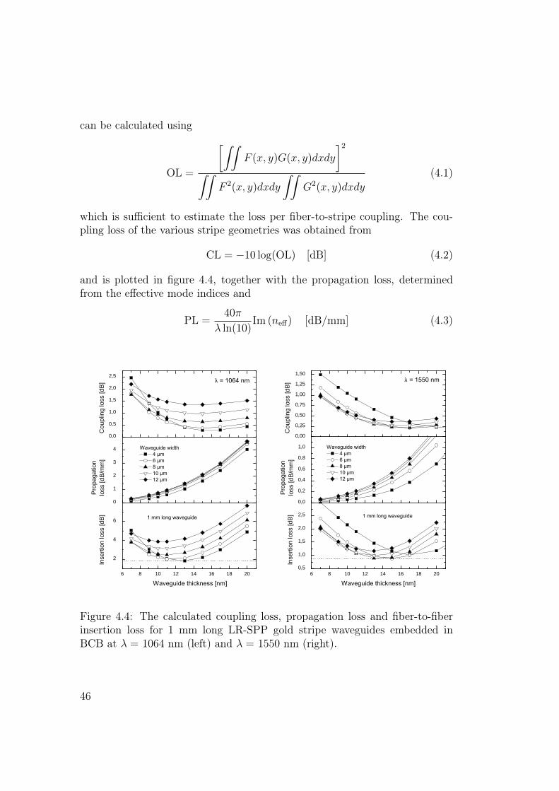
can be calculated using
OL =
[∫∫F (x, y)G(x, y)dxdy
]2
∫∫F 2(x, y)dxdy
∫∫G2(x, y)dxdy
(4.1)
which is sufficient to estimate the loss per fiber-to-stripe coupling. The cou-pling loss of the various stripe geometries was obtained from
CL = −10 log(OL) [dB] (4.2)
and is plotted in figure 4.4, together with the propagation loss, determinedfrom the effective mode indices and
PL =40π
λ ln(10)Im (neff) [dB/mm] (4.3)
0 , 00 , 51 , 01 , 52 , 02 , 5
Coup
ling lo
ss [dB
] ���������
01
234 ��������������
���������������������������
�
Propa
gatio
nlos
s [dB
/mm]
6 8 1 0 1 2 1 4 1 6 1 8 2 0
2
4
6
������������� ���������
Insert
ion lo
ss [dB
] �������������������
0 , 0 00 , 2 50 , 5 00 , 7 51 , 0 01 , 2 51 , 5 0
Coup
ling lo
ss [dB
] ��������
0 , 00 , 20 , 40 , 60 , 81 , 0 �������������
���������������������������
�
Propa
gatio
nlos
s [dB
/mm]
6 8 1 0 1 2 1 4 1 6 1 8 2 00 , 5
1 , 0
1 , 5
2 , 0
2 , 5
����������������������
Insert
ion lo
ss [dB
] ����������� �������
Figure 4.4: The calculated coupling loss, propagation loss and fiber-to-fiberinsertion loss for 1 mm long LR-SPP gold stripe waveguides embedded inBCB at λ = 1064 nm (left) and λ = 1550 nm (right).
46
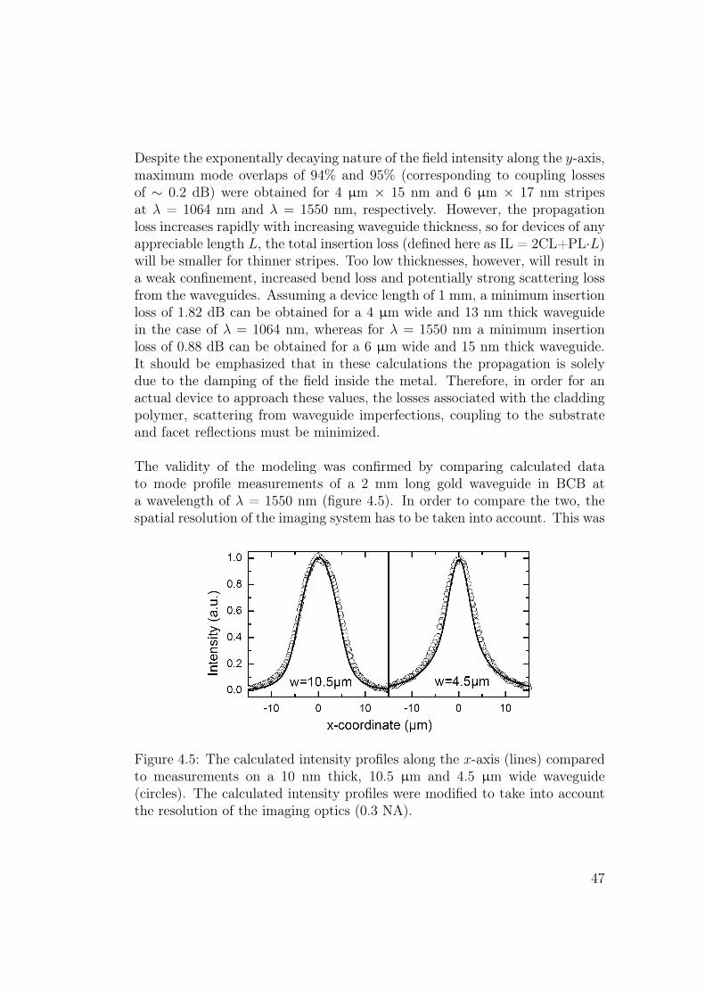
Despite the exponentally decaying nature of the field intensity along the y-axis,maximum mode overlaps of 94% and 95% (corresponding to coupling lossesof ∼ 0.2 dB) were obtained for 4 µm × 15 nm and 6 µm × 17 nm stripesat λ = 1064 nm and λ = 1550 nm, respectively. However, the propagationloss increases rapidly with increasing waveguide thickness, so for devices of anyappreciable length L, the total insertion loss (defined here as IL = 2CL+PL·L)will be smaller for thinner stripes. Too low thicknesses, however, will result ina weak confinement, increased bend loss and potentially strong scattering lossfrom the waveguides. Assuming a device length of 1 mm, a minimum insertionloss of 1.82 dB can be obtained for a 4 µm wide and 13 nm thick waveguidein the case of λ = 1064 nm, whereas for λ = 1550 nm a minimum insertionloss of 0.88 dB can be obtained for a 6 µm wide and 15 nm thick waveguide.It should be emphasized that in these calculations the propagation is solelydue to the damping of the field inside the metal. Therefore, in order for anactual device to approach these values, the losses associated with the claddingpolymer, scattering from waveguide imperfections, coupling to the substrateand facet reflections must be minimized.
The validity of the modeling was confirmed by comparing calculated datato mode profile measurements of a 2 mm long gold waveguide in BCB ata wavelength of λ = 1550 nm (figure 4.5). In order to compare the two, thespatial resolution of the imaging system has to be taken into account. This was
Figure 4.5: The calculated intensity profiles along the x-axis (lines) comparedto measurements on a 10 nm thick, 10.5 µm and 4.5 µm wide waveguide(circles). The calculated intensity profiles were modified to take into accountthe resolution of the imaging optics (0.3 NA).
47
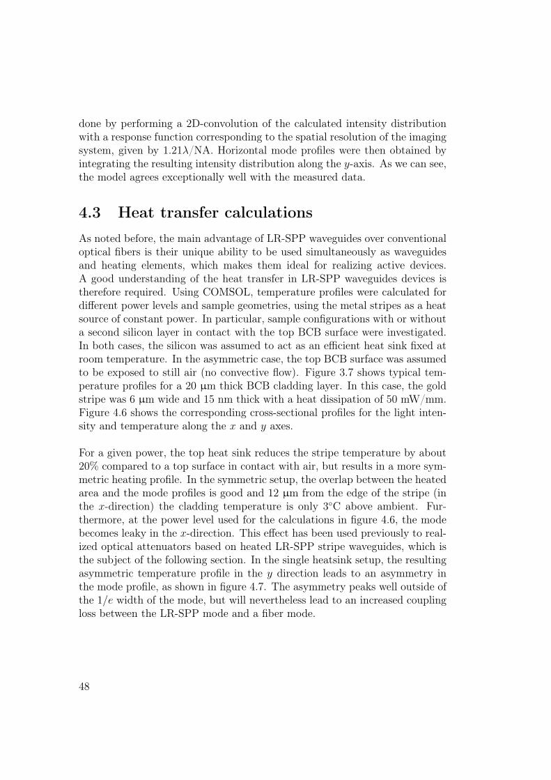
done by performing a 2D-convolution of the calculated intensity distributionwith a response function corresponding to the spatial resolution of the imagingsystem, given by 1.21λ/NA. Horizontal mode profiles were then obtained byintegrating the resulting intensity distribution along the y-axis. As we can see,the model agrees exceptionally well with the measured data.
4.3 Heat transfer calculationsAs noted before, the main advantage of LR-SPP waveguides over conventionaloptical fibers is their unique ability to be used simultaneously as waveguidesand heating elements, which makes them ideal for realizing active devices.A good understanding of the heat transfer in LR-SPP waveguides devices istherefore required. Using COMSOL, temperature profiles were calculated fordifferent power levels and sample geometries, using the metal stripes as a heatsource of constant power. In particular, sample configurations with or withouta second silicon layer in contact with the top BCB surface were investigated.In both cases, the silicon was assumed to act as an efficient heat sink fixed atroom temperature. In the asymmetric case, the top BCB surface was assumedto be exposed to still air (no convective flow). Figure 3.7 shows typical tem-perature profiles for a 20 µm thick BCB cladding layer. In this case, the goldstripe was 6 µm wide and 15 nm thick with a heat dissipation of 50 mW/mm.Figure 4.6 shows the corresponding cross-sectional profiles for the light inten-sity and temperature along the x and y axes.
For a given power, the top heat sink reduces the stripe temperature by about20% compared to a top surface in contact with air, but results in a more sym-metric heating profile. In the symmetric setup, the overlap between the heatedarea and the mode profiles is good and 12 µm from the edge of the stripe (inthe x-direction) the cladding temperature is only 3◦C above ambient. Fur-thermore, at the power level used for the calculations in figure 4.6, the modebecomes leaky in the x-direction. This effect has been used previously to real-ized optical attenuators based on heated LR-SPP stripe waveguides, which isthe subject of the following section. In the single heatsink setup, the resultingasymmetric temperature profile in the y direction leads to an asymmetry inthe mode profile, as shown in figure 4.7. The asymmetry peaks well outside ofthe 1/e width of the mode, but will nevertheless lead to an increased couplingloss between the LR-SPP mode and a fiber mode.
48
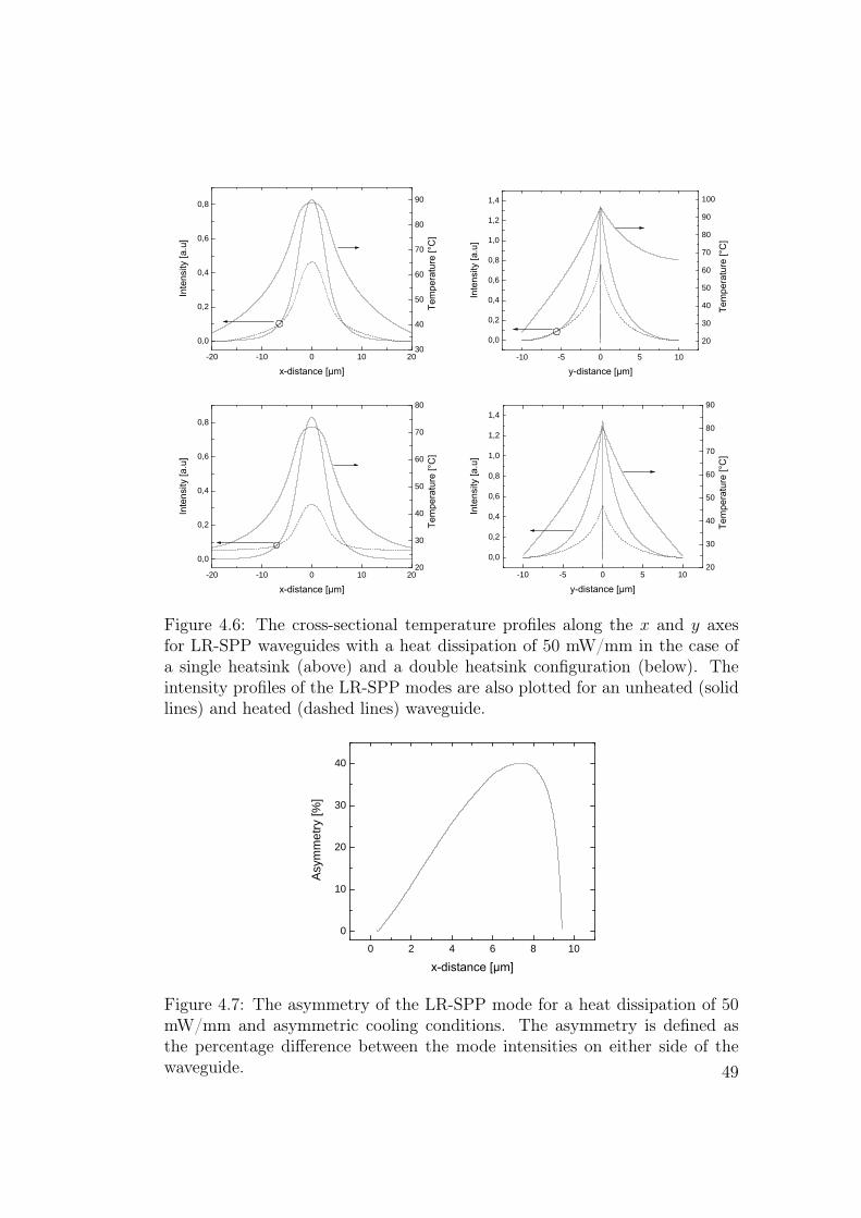
- 2 0 - 1 0 0 1 0 2 00 , 0
0 , 2
0 , 4
0 , 6
0 , 8
3 0
4 0
5 0
6 0
7 0
8 0
9 0
����
����
������
���� ��������
���
�����
����
�
- 1 0 - 5 0 5 1 00 , 00 , 20 , 40 , 60 , 81 , 01 , 21 , 4
2 03 04 05 06 07 08 09 01 0 0
�
����
������
���
���� ��������
��
�����
����
�
- 2 0 - 1 0 0 1 0 2 00 , 0
0 , 2
0 , 4
0 , 6
0 , 8
2 0
3 0
4 0
5 0
6 0
7 0
8 0�
����
������
���
���� ��������
���
�����
����
�
- 1 0 - 5 0 5 1 00 , 00 , 20 , 40 , 60 , 81 , 01 , 21 , 4
2 0
3 0
4 0
5 0
6 0
7 0
8 0
9 0�
����
������
���
���� ��������
��
�����
����
�
Figure 4.6: The cross-sectional temperature profiles along the x and y axesfor LR-SPP waveguides with a heat dissipation of 50 mW/mm in the case ofa single heatsink (above) and a double heatsink configuration (below). Theintensity profiles of the LR-SPP modes are also plotted for an unheated (solidlines) and heated (dashed lines) waveguide.
0 2 4 6 8 1 00
1 0
2 0
3 0
4 0
Asym
metry
[%]
���� ��������
Figure 4.7: The asymmetry of the LR-SPP mode for a heat dissipation of 50mW/mm and asymmetric cooling conditions. The asymmetry is defined asthe percentage difference between the mode intensities on either side of thewaveguide. 49
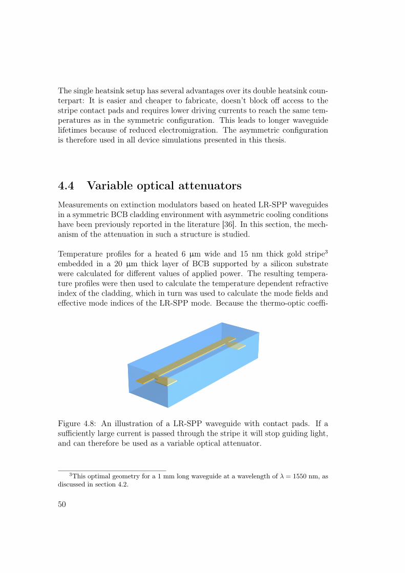
The single heatsink setup has several advantages over its double heatsink coun-terpart: It is easier and cheaper to fabricate, doesn’t block off access to thestripe contact pads and requires lower driving currents to reach the same tem-peratures as in the symmetric configuration. This leads to longer waveguidelifetimes because of reduced electromigration. The asymmetric configurationis therefore used in all device simulations presented in this thesis.
4.4 Variable optical attenuatorsMeasurements on extinction modulators based on heated LR-SPP waveguidesin a symmetric BCB cladding environment with asymmetric cooling conditionshave been previously reported in the literature [36]. In this section, the mech-anism of the attenuation in such a structure is studied.
Temperature profiles for a heated 6 µm wide and 15 nm thick gold stripe3embedded in a 20 µm thick layer of BCB supported by a silicon substratewere calculated for different values of applied power. The resulting tempera-ture profiles were then used to calculate the temperature dependent refractiveindex of the cladding, which in turn was used to calculate the mode fields andeffective mode indices of the LR-SPP mode. Because the thermo-optic coeffi-
Figure 4.8: An illustration of a LR-SPP waveguide with contact pads. If asufficiently large current is passed through the stripe it will stop guiding light,and can therefore be used as a variable optical attenuator.
3This optimal geometry for a 1 mm long waveguide at a wavelength of λ = 1550 nm, asdiscussed in section 4.2.
50
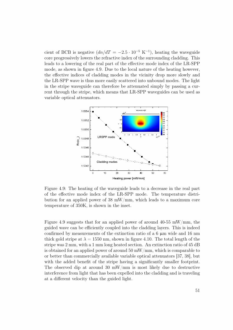
cient of BCB is negative (dn/dT = −2.5 · 10−5 K−1), heating the waveguidecore progressively lowers the refractive index of the surrounding cladding. Thisleads to a lowering of the real part of the effective mode index of the LR-SPPmode, as shown in figure 4.9. Due to the local nature of the heating however,the effective indices of cladding modes in the vicinity drop more slowly andthe LR-SPP wave is thus more easily scattered into unbound modes. The lightin the stripe waveguide can therefore be attenuated simply by passing a cur-rent through the stripe, which means that LR-SPP waveguides can be used asvariable optical attenuators.
Figure 4.9: The heating of the waveguide leads to a decrease in the real partof the effective mode index of the LR-SPP mode. The temperature distri-bution for an applied power of 38 mW/mm, which leads to a maximum coretemperature of 350K, is shown in the inset.
Figure 4.9 suggests that for an applied power of around 40-55 mW/mm, theguided wave can be efficiently coupled into the cladding layers. This is indeedconfirmed by measurements of the extinction ratio of a 6 µm wide and 16 nmthick gold stripe at λ = 1550 nm, shown in figure 4.10. The total length of thestripe was 2 mm, with a 1 mm long heated section. An extinction ratio of 45 dBis obtained for an applied power of around 50 mW/mm, which is comparable toor better than commercially available variable optical attenuators [37, 38], butwith the added benefit of the stripe having a significantly smaller footprint.The observed dip at around 30 mW/mm is most likely due to destructiveinterference from light that has been expelled into the cladding and is travelingat a different velocity than the guided light.
51
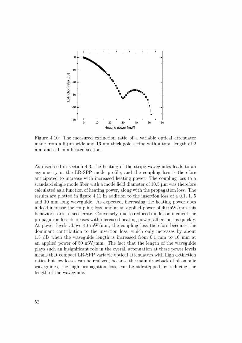
0 10 20 30 40 50 60-50
-40
-30
-20
-10
0
Ext
inct
ion
ratio
[dB
]
Heating power [mW]
Figure 4.10: The measured extinction ratio of a variable optical attenuatormade from a 6 µm wide and 16 nm thick gold stripe with a total length of 2mm and a 1 mm heated section.
As discussed in section 4.3, the heating of the stripe waveguides leads to anasymmetry in the LR-SPP mode profile, and the coupling loss is thereforeanticipated to increase with increased heating power. The coupling loss to astandard single mode fiber with a mode field diameter of 10.5 µm was thereforecalculated as a function of heating power, along with the propagation loss. Theresults are plotted in figure 4.11 in addition to the insertion loss of a 0.1, 1, 5and 10 mm long waveguide. As expected, increasing the heating power doesindeed increase the coupling loss, and at an applied power of 40 mW/mm thisbehavior starts to accelerate. Conversely, due to reduced mode confinement thepropagation loss decreases with increased heating power, albeit not as quickly.At power levels above 40 mW/mm, the coupling loss therefore becomes thedominant contribution to the insertion loss, which only increases by about1.5 dB when the waveguide length is increased from 0.1 mm to 10 mm atan applied power of 50 mW/mm. The fact that the length of the waveguideplays such an insignificant role in the overall attenuation at these power levelsmeans that compact LR-SPP variable optical attenuators with high extinctionratios but low losses can be realized, because the main drawback of plasmonicwaveguides, the high propagation loss, can be sidestepped by reducing thelength of the waveguide.
52
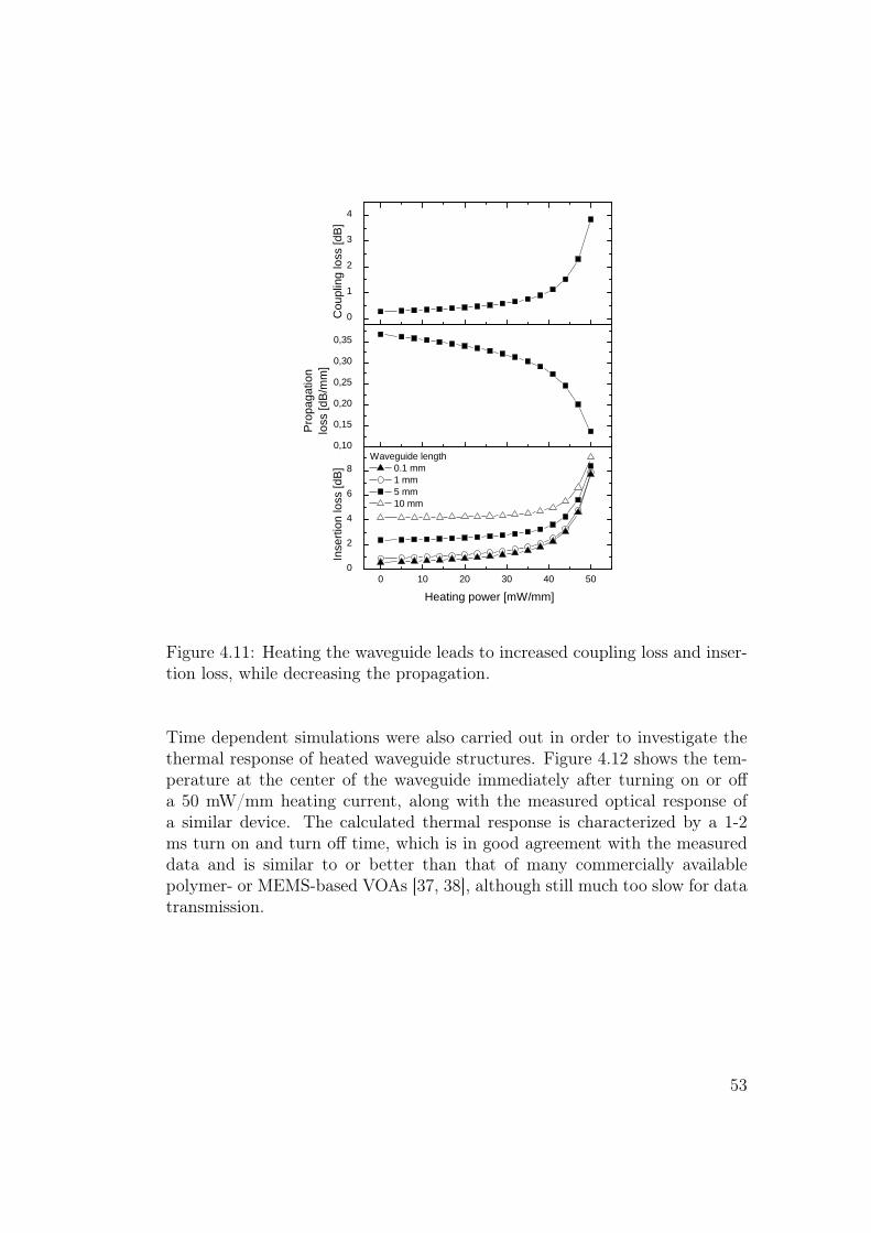
0
1
2
3
4
Coup
ling lo
ss [dB
]
0 , 1 00 , 1 50 , 2 00 , 2 50 , 3 00 , 3 5
Propa
gatio
nlos
s [dB
/mm]
0 1 0 2 0 3 0 4 0 5 00
2
4
6
8
Inse
rtion l
oss [
dB] W a v e g u i d e l e n g t h
0 . 1 m m 1 m m 5 m m 1 0 m m
H e a t i n g p o w e r [ m W / m m ]
Figure 4.11: Heating the waveguide leads to increased coupling loss and inser-tion loss, while decreasing the propagation.
Time dependent simulations were also carried out in order to investigate thethermal response of heated waveguide structures. Figure 4.12 shows the tem-perature at the center of the waveguide immediately after turning on or offa 50 mW/mm heating current, along with the measured optical response ofa similar device. The calculated thermal response is characterized by a 1-2ms turn on and turn off time, which is in good agreement with the measureddata and is similar to or better than that of many commercially availablepolymer- or MEMS-based VOAs [37, 38], although still much too slow for datatransmission.
53
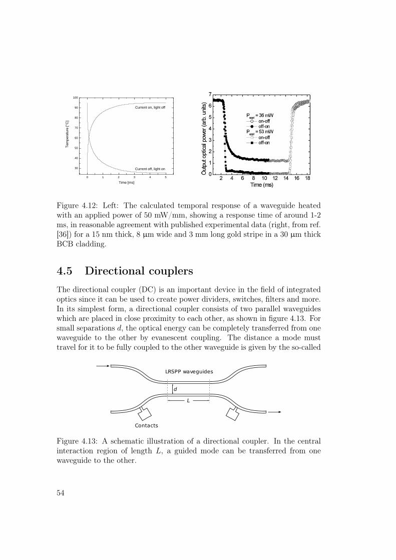
0 1 2 3 4 5
3 0
4 0
5 0
6 0
7 0
8 0
9 0
1 0 0
�
���
����
��� �
�
T i m e [ m s ]
C u r r e n t o n , l i g h t o f f
C u r r e n t o f f , l i g h t o n
Figure 4.12: Left: The calculated temporal response of a waveguide heatedwith an applied power of 50 mW/mm, showing a response time of around 1-2ms, in reasonable agreement with published experimental data (right, from ref.[36]) for a 15 nm thick, 8 µm wide and 3 mm long gold stripe in a 30 µm thickBCB cladding.
4.5 Directional couplersThe directional coupler (DC) is an important device in the field of integratedoptics since it can be used to create power dividers, switches, filters and more.In its simplest form, a directional coupler consists of two parallel waveguideswhich are placed in close proximity to each other, as shown in figure 4.13. Forsmall separations d, the optical energy can be completely transferred from onewaveguide to the other by evanescent coupling. The distance a mode musttravel for it to be fully coupled to the other waveguide is given by the so-called
L
d
Contacts
LRSPP waveguides
Figure 4.13: A schematic illustration of a directional coupler. In the centralinteraction region of length L, a guided mode can be transferred from onewaveguide to the other.
54
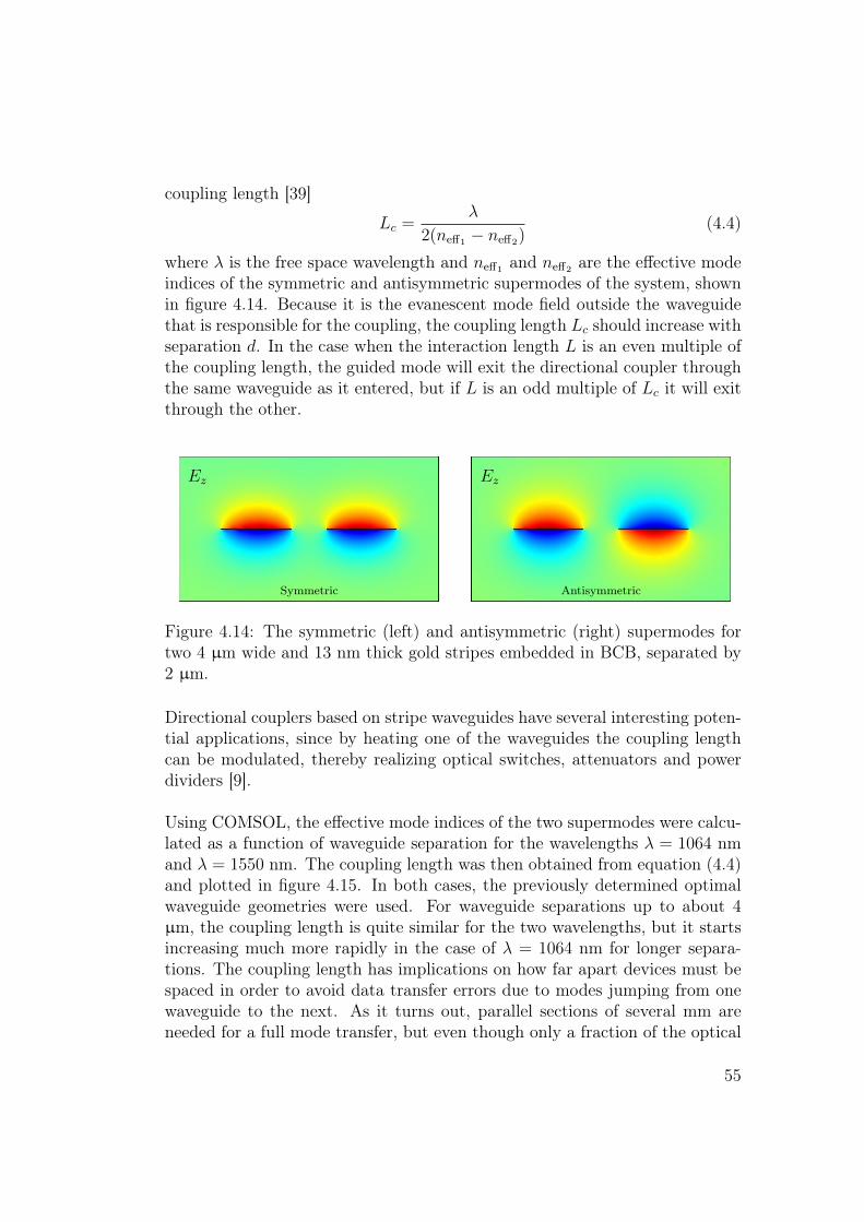
coupling length [39]
Lc =λ
2(neff1 − neff2)(4.4)
where λ is the free space wavelength and neff1 and neff2 are the effective modeindices of the symmetric and antisymmetric supermodes of the system, shownin figure 4.14. Because it is the evanescent mode field outside the waveguidethat is responsible for the coupling, the coupling length Lc should increase withseparation d. In the case when the interaction length L is an even multiple ofthe coupling length, the guided mode will exit the directional coupler throughthe same waveguide as it entered, but if L is an odd multiple of Lc it will exitthrough the other.
Symmetric Antisymmetric
Ez Ez
Figure 4.14: The symmetric (left) and antisymmetric (right) supermodes fortwo 4 µm wide and 13 nm thick gold stripes embedded in BCB, separated by2 µm.
Directional couplers based on stripe waveguides have several interesting poten-tial applications, since by heating one of the waveguides the coupling lengthcan be modulated, thereby realizing optical switches, attenuators and powerdividers [9].
Using COMSOL, the effective mode indices of the two supermodes were calcu-lated as a function of waveguide separation for the wavelengths λ = 1064 nmand λ = 1550 nm. The coupling length was then obtained from equation (4.4)and plotted in figure 4.15. In both cases, the previously determined optimalwaveguide geometries were used. For waveguide separations up to about 4µm, the coupling length is quite similar for the two wavelengths, but it startsincreasing much more rapidly in the case of λ = 1064 nm for longer separa-tions. The coupling length has implications on how far apart devices must bespaced in order to avoid data transfer errors due to modes jumping from onewaveguide to the next. As it turns out, parallel sections of several mm areneeded for a full mode transfer, but even though only a fraction of the optical
55
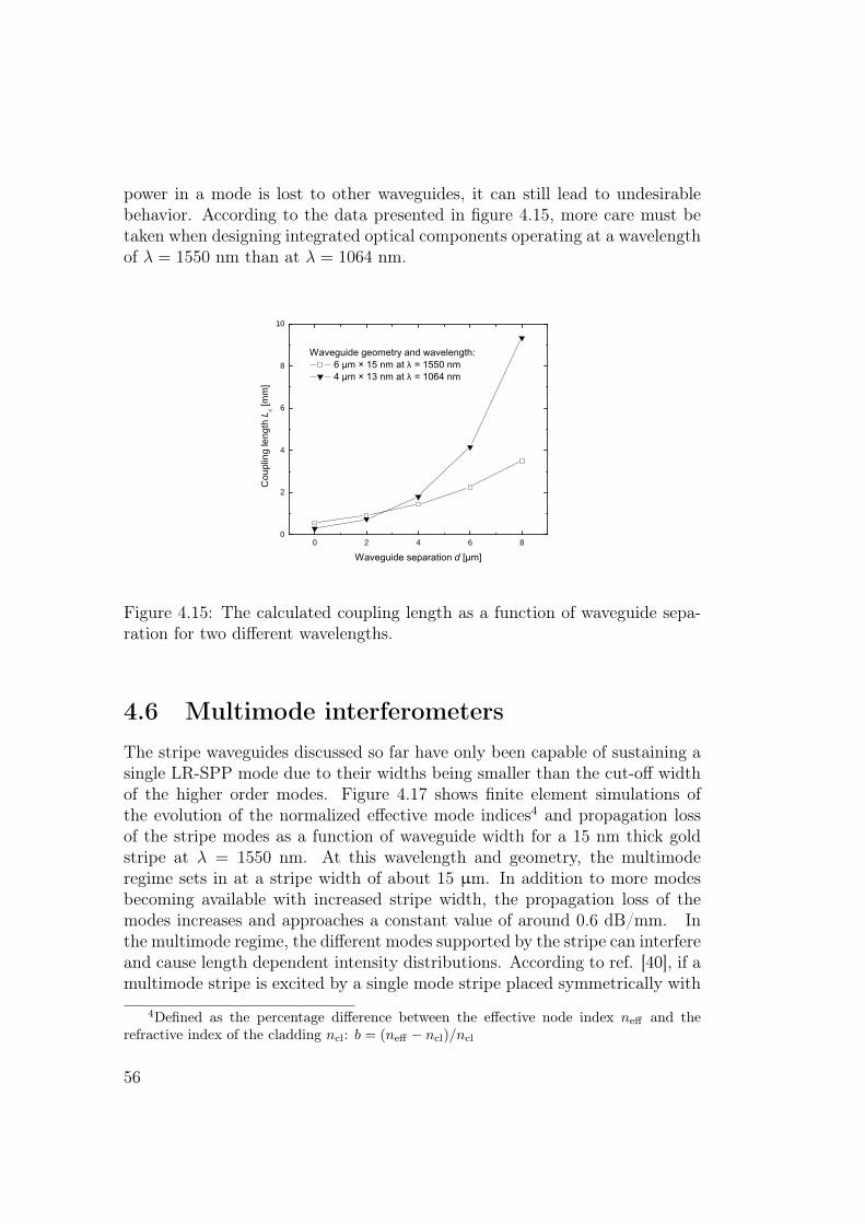
power in a mode is lost to other waveguides, it can still lead to undesirablebehavior. According to the data presented in figure 4.15, more care must betaken when designing integrated optical components operating at a wavelengthof λ = 1550 nm than at λ = 1064 nm.
0 2 4 6 80
2
4
6
8
1 0�
����������������� ���� ��������������� ������� ���������������� ������� ����������
Coup
ling le
ngth
L c [mm]
����������� � �����d �����
Figure 4.15: The calculated coupling length as a function of waveguide sepa-ration for two different wavelengths.
4.6 Multimode interferometersThe stripe waveguides discussed so far have only been capable of sustaining asingle LR-SPP mode due to their widths being smaller than the cut-off widthof the higher order modes. Figure 4.17 shows finite element simulations ofthe evolution of the normalized effective mode indices4 and propagation lossof the stripe modes as a function of waveguide width for a 15 nm thick goldstripe at λ = 1550 nm. At this wavelength and geometry, the multimoderegime sets in at a stripe width of about 15 µm. In addition to more modesbecoming available with increased stripe width, the propagation loss of themodes increases and approaches a constant value of around 0.6 dB/mm. Inthe multimode regime, the different modes supported by the stripe can interfereand cause length dependent intensity distributions. According to ref. [40], if amultimode stripe is excited by a single mode stripe placed symmetrically with
4Defined as the percentage difference between the effective node index neff and therefractive index of the cladding ncl: b = (neff − ncl)/ncl
56
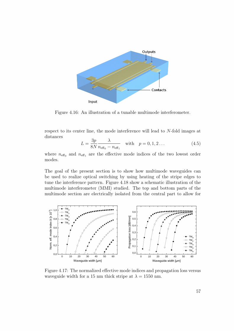
Figure 4.16: An illustration of a tunable multimode interferometer.
respect to its center line, the mode interference will lead to N -fold images atdistances
L =3p
8N
λ
neff0 − neff1
with p = 0, 1, 2 . . . (4.5)
where neff0 and neff1 are the effective mode indices of the two lowest ordermodes.
The goal of the present section is to show how multimode waveguides canbe used to realize optical switching by using heating of the stripe edges totune the interference pattern. Figure 4.18 show a schematic illustration of themultimode interferometer (MMI) studied. The top and bottom parts of themultimode section are electrically isolated from the central part to allow for
0 1 0 2 0 3 0 4 0 5 0 6 00 , 0
0 , 2
0 , 4
0 , 6
0 , 8
1 , 0
�
�������������������������
Norm
. eff.
mode
inde
x b [x
10-3 ]
������ ���� ������0 1 0 2 0 3 0 4 0 5 0 6 0
0 , 0
0 , 1
0 , 2
0 , 3
0 , 4
0 , 5
0 , 6
�
Propa
gatio
n los
s [dB
/mm]
������ ���� ������
�������������������������
Figure 4.17: The normalized effective mode indices and propagation loss versuswaveguide width for a 15 nm thick stripe at λ = 1550 nm.
57
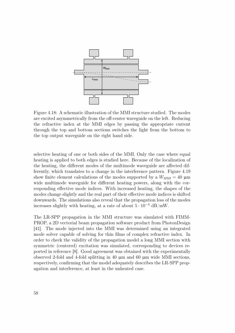
WMMI
LMMI
Figure 4.18: A schematic illustration of the MMI structure studied. The modesare excited asymmetrically from the off-center waveguide on the left. Reducingthe refractive index at the MMI edges by passing the appropriate currentthrough the top and bottom sections switches the light from the bottom tothe top output waveguide on the right hand side.
selective heating of one or both sides of the MMI. Only the case where equalheating is applied to both edges is studied here. Because of the localization ofthe heating, the different modes of the multimode waveguide are affected dif-ferently, which translates to a change in the interference pattern. Figure 4.19show finite element calculations of the modes supported by a WMMI = 40 µmwide multimode waveguide for different heating powers, along with the cor-responding effective mode indices. With increased heating, the shapes of themodes change slightly and the real part of their effective mode indices is shifteddownwards. The simulations also reveal that the propagation loss of the modesincreases slightly with heating, at a rate of about 5 · 10−3 dB/mW.
The LR-SPP propagation in the MMI structure was simulated with FIMM-PROP, a 2D vectorial beam propagation software product from PhotonDesign[41]. The mode injected into the MMI was determined using an integratedmode solver capable of solving for thin films of complex refractive index. Inorder to check the validity of the propagation model a long MMI section withsymmetric (centered) excitation was simulated, corresponding to devices re-ported in reference [8]. Good agreement was obtained with the experimentallyobserved 2-fold and 4-fold splitting in 40 µm and 60 µm wide MMI sections,respectively, confirming that the model adequately describes the LR-SPP prop-agation and interference, at least in the unheated case.
58
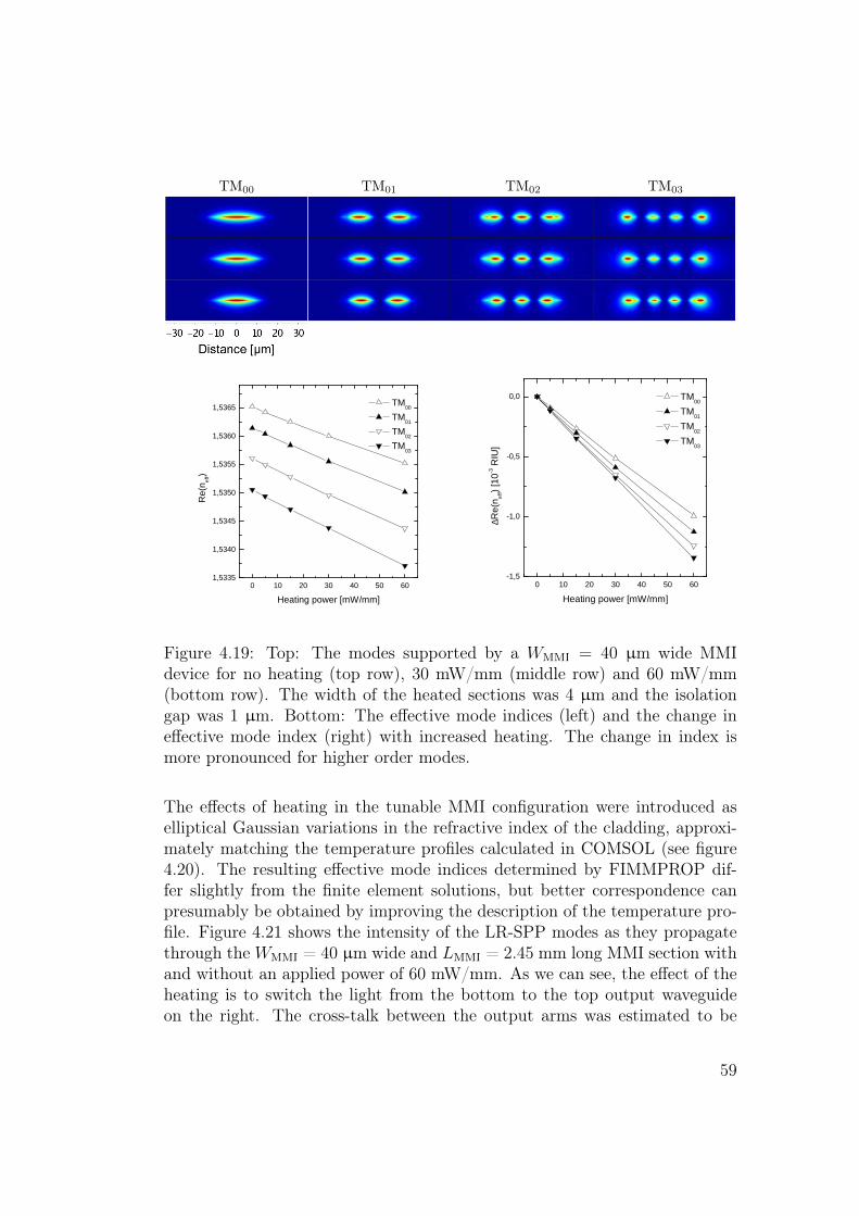
TM00 TM01 TM02 TM03
0 1 0 2 0 3 0 4 0 5 0 6 01 , 5 3 3 5
1 , 5 3 4 0
1 , 5 3 4 5
1 , 5 3 5 0
1 , 5 3 5 5
1 , 5 3 6 0
1 , 5 3 6 5
Re(n eff
)
H e a t i n g p o w e r [ m W / m m ]
T M 0 0 T M 0 1 T M 0 2 T M 0 3
0 1 0 2 0 3 0 4 0 5 0 6 0- 1 , 5
- 1 , 0
- 0 , 5
0 , 0
∆Re(n
eff) [1
0-3 RIU]
H e a t i n g p o w e r [ m W / m m ]
T M 0 0 T M 0 1 T M 0 2 T M 0 3
Figure 4.19: Top: The modes supported by a WMMI = 40 µm wide MMIdevice for no heating (top row), 30 mW/mm (middle row) and 60 mW/mm(bottom row). The width of the heated sections was 4 µm and the isolationgap was 1 µm. Bottom: The effective mode indices (left) and the change ineffective mode index (right) with increased heating. The change in index ismore pronounced for higher order modes.
The effects of heating in the tunable MMI configuration were introduced aselliptical Gaussian variations in the refractive index of the cladding, approxi-mately matching the temperature profiles calculated in COMSOL (see figure4.20). The resulting effective mode indices determined by FIMMPROP dif-fer slightly from the finite element solutions, but better correspondence canpresumably be obtained by improving the description of the temperature pro-file. Figure 4.21 shows the intensity of the LR-SPP modes as they propagatethrough theWMMI = 40 µm wide and LMMI = 2.45 mm long MMI section withand without an applied power of 60 mW/mm. As we can see, the effect of theheating is to switch the light from the bottom to the top output waveguideon the right. The cross-talk between the output arms was estimated to be
59
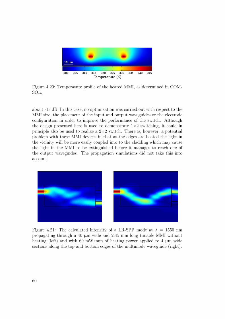
Figure 4.20: Temperature profile of the heated MMI, as determined in COM-SOL.
about -13 dB. In this case, no optimization was carried out with respect to theMMI size, the placement of the input and output waveguides or the electrodeconfiguration in order to improve the performance of the switch. Althoughthe design presented here is used to demonstrate 1×2 switching, it could inprinciple also be used to realize a 2×2 switch. There is, however, a potentialproblem with these MMI devices in that as the edges are heated the light inthe vicinity will be more easily coupled into to the cladding which may causethe light in the MMI to be extinguished before it manages to reach one ofthe output waveguides. The propagation simulations did not take this intoaccount.
Figure 4.21: The calculated intensity of a LR-SPP mode at λ = 1550 nmpropagating through a 40 µm wide and 2.45 mm long tunable MMI withoutheating (left) and with 60 mW/mm of heating power applied to 4 µm widesections along the top and bottom edges of the multimode waveguide (right).
60

It should be kept in mind that because LR-SPP waveguides can only transmitTM polarized light, they are only useful in a limited number of cases (e.g. inlaser modules). LR-SPP waveguides with square cross-sections on the otherhand, have been show to transmit arbitrarily polarized light [11, 42], and arethe focus of the next chapter.
61

62
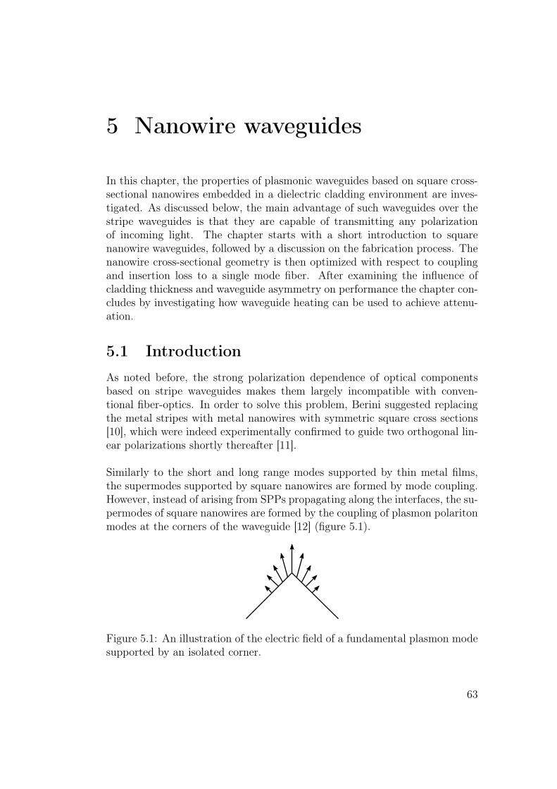
5 Nanowire waveguides
In this chapter, the properties of plasmonic waveguides based on square cross-sectional nanowires embedded in a dielectric cladding environment are inves-tigated. As discussed below, the main advantage of such waveguides over thestripe waveguides is that they are capable of transmitting any polarizationof incoming light. The chapter starts with a short introduction to squarenanowire waveguides, followed by a discussion on the fabrication process. Thenanowire cross-sectional geometry is then optimized with respect to couplingand insertion loss to a single mode fiber. After examining the influence ofcladding thickness and waveguide asymmetry on performance the chapter con-cludes by investigating how waveguide heating can be used to achieve attenu-ation.
5.1 IntroductionAs noted before, the strong polarization dependence of optical componentsbased on stripe waveguides makes them largely incompatible with conven-tional fiber-optics. In order to solve this problem, Berini suggested replacingthe metal stripes with metal nanowires with symmetric square cross sections[10], which were indeed experimentally confirmed to guide two orthogonal lin-ear polarizations shortly thereafter [11].
Similarly to the short and long range modes supported by thin metal films,the supermodes supported by square nanowires are formed by mode coupling.However, instead of arising from SPPs propagating along the interfaces, the su-permodes of square nanowires are formed by the coupling of plasmon polaritonmodes at the corners of the waveguide [12] (figure 5.1).
Figure 5.1: An illustration of the electric field of a fundamental plasmon modesupported by an isolated corner.
63
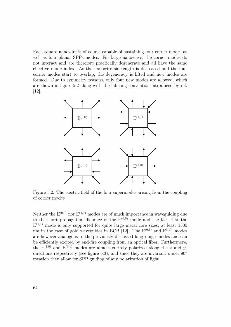
Each square nanowire is of course capable of sustaining four corner modes aswell as four planar SPPs modes. For large nanowires, the corner modes donot interact and are therefore practically degenerate and all have the sameeffective mode index. As the nanowire sidelength is decreased and the fourcorner modes start to overlap, the degeneracy is lifted and new modes areformed. Due to symmetry reasons, only four new modes are allowed, whichare shown in figure 5.2 along with the labeling convention introduced by ref.[12].
E(0,0) E(1,1)
E(0,1) E(1,0)
Figure 5.2: The electric field of the four supermodes arising from the couplingof corner modes.
Neither the E(0,0) nor E(1,1) modes are of much importance in waveguiding dueto the short propagation distance of the E(0,0) mode and the fact that theE(1,1) mode is only supported for quite large metal core sizes, at least 1500nm in the case of gold waveguides in BCB [12]. The E(0,1) and E(1,0) modesare however analogous to the previously discussed long range modes and canbe efficiently excited by end-fire coupling from an optical fiber. Furthermore,the E(1,0) and E(0,1) modes are almost entirely polarized along the x and y-directions respectively (see figure 5.3), and since they are invariant under 90◦rotation they allow for SPP guiding of any polarization of light.
64
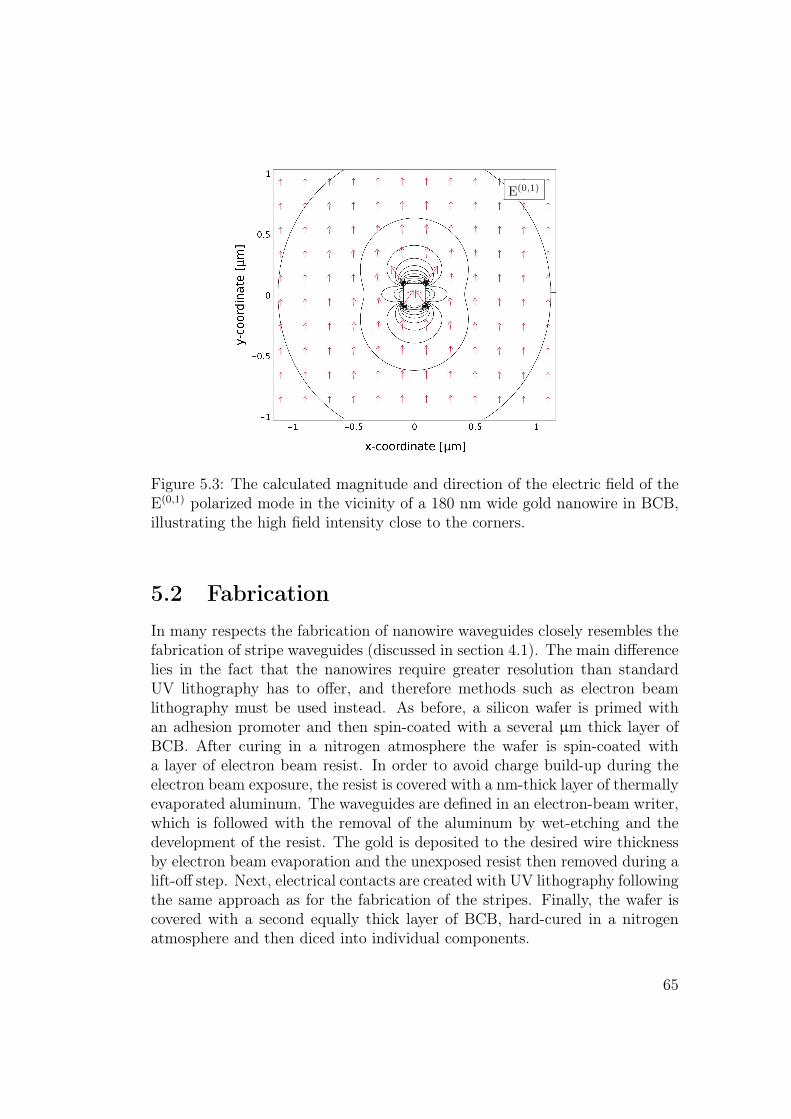
E(0,1)
Figure 5.3: The calculated magnitude and direction of the electric field of theE(0,1) polarized mode in the vicinity of a 180 nm wide gold nanowire in BCB,illustrating the high field intensity close to the corners.
5.2 FabricationIn many respects the fabrication of nanowire waveguides closely resembles thefabrication of stripe waveguides (discussed in section 4.1). The main differencelies in the fact that the nanowires require greater resolution than standardUV lithography has to offer, and therefore methods such as electron beamlithography must be used instead. As before, a silicon wafer is primed withan adhesion promoter and then spin-coated with a several µm thick layer ofBCB. After curing in a nitrogen atmosphere the wafer is spin-coated witha layer of electron beam resist. In order to avoid charge build-up during theelectron beam exposure, the resist is covered with a nm-thick layer of thermallyevaporated aluminum. The waveguides are defined in an electron-beam writer,which is followed with the removal of the aluminum by wet-etching and thedevelopment of the resist. The gold is deposited to the desired wire thicknessby electron beam evaporation and the unexposed resist then removed during alift-off step. Next, electrical contacts are created with UV lithography followingthe same approach as for the fabrication of the stripes. Finally, the wafer iscovered with a second equally thick layer of BCB, hard-cured in a nitrogenatmosphere and then diced into individual components.
65
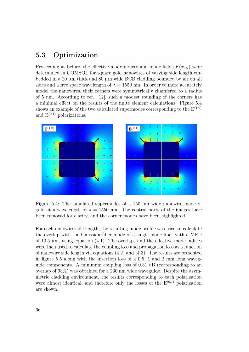
5.3 OptimizationProceeding as before, the effective mode indices and mode fields F (x, y) weredetermined in COMSOL for square gold nanowires of varying side length em-bedded in a 20 µm thick and 80 µm wide BCB cladding bounded by air on allsides and a free space wavelength of λ = 1550 nm. In order to more accuratelymodel the nanowires, their corners were symmetrically chamfered to a radiusof 5 nm. According to ref. [12], such a modest rounding of the corners hasa minimal effect on the results of the finite element calculations. Figure 5.4shows an example of the two calculated supermodes corresponding to the E(1,0)
and E(0,1) polarizations.
E(1,0) E(0,1)
Figure 5.4: The simulated supermodes of a 150 nm wide nanowire made ofgold at a wavelength of λ = 1550 nm. The central parts of the images havebeen removed for clarity, and the corner modes have been highlighted.
For each nanowire side length, the resulting mode profile was used to calculatethe overlap with the Gaussian fiber mode of a single mode fiber with a MFDof 10.5 µm, using equation (4.1). The overlaps and the effective mode indiceswere then used to calculate the coupling loss and propagation loss as a functionof nanowire side length via equations (4.2) and (4.3). The results are presentedin figure 5.5 along with the insertion loss of a 0.5, 1 and 2 mm long waveg-uide components. A minimum coupling loss of 0.31 dB (corresponding to anoverlap of 93%) was obtained for a 230 nm wide waveguide. Despite the asym-metric cladding environment, the results corresponding to each polarizationwere almost identical, and therefore only the losses of the E(0,1) polarizationare shown.
66
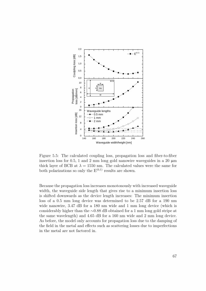
0 , 0
0 , 5
1 , 0
1 , 5
2 , 0
Coulp
ling lo
ss [dB
]
02468
1 0
E ( 0 , 1 )
Propa
gatio
nlos
s [dB
/mm]
1 4 0 1 6 0 1 8 0 2 0 0 2 2 0 2 4 0 2 6 00
4
8
1 2
1 6 W a v e g u i d e l e n g t h s 0 . 5 m m 1 m m 2 m m
W a v e g u i d e w i d t h / h e i g h t [ n m ]
Insert
ion lo
ss [dB
]
w
hH
W
Au
BCB
Figure 5.5: The calculated coupling loss, propagation loss and fiber-to-fiberinsertion loss for 0.5, 1 and 2 mm long gold nanowire waveguides in a 20 µmthick layer of BCB at λ = 1550 nm. The calculated values were the same forboth polarizations so only the E(0,1) results are shown.
Because the propagation loss increases monotonously with increased waveguidewidth, the waveguide side length that gives rise to a minimum insertion lossis shifted downwards as the device length increases: The minimum insertionloss of a 0.5 mm long device was determined to be 2.57 dB for a 190 nmwide nanowire, 3.47 dB for a 180 nm wide and 1 mm long device (which isconsiderably higher than the ∼0.88 dB obtained for a 1 mm long gold stripe atthe same wavelength) and 4.65 dB for a 160 nm wide and 2 mm long device.As before, the model only accounts for propagation loss due to the damping ofthe field in the metal and effects such as scattering losses due to imperfectionsin the metal are not factored in.
67
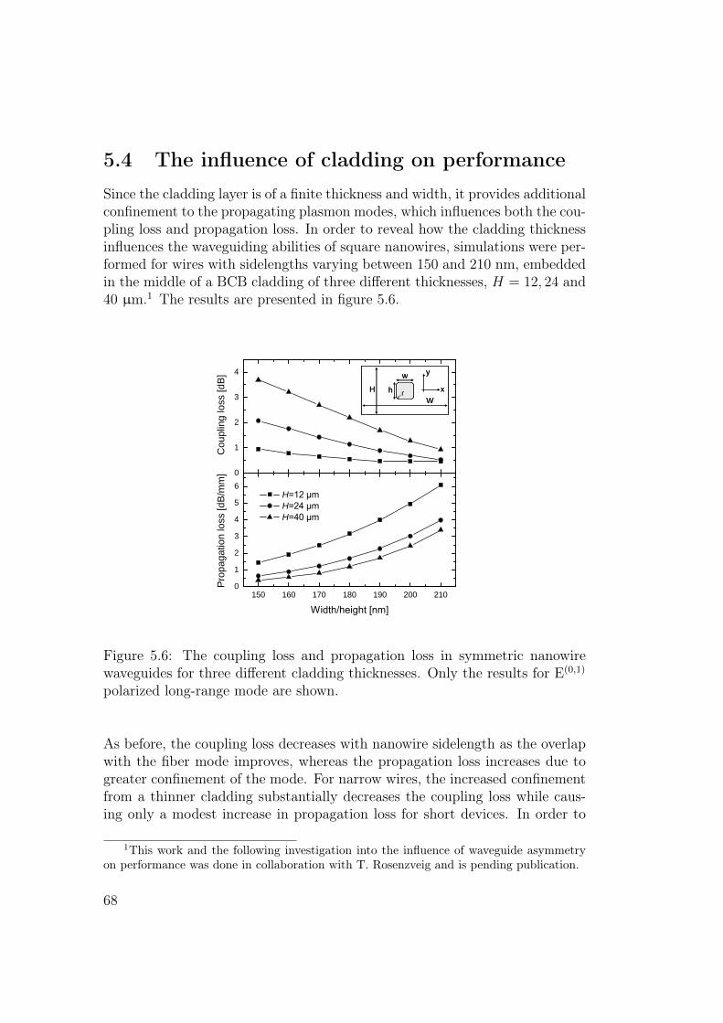
5.4 The influence of cladding on performanceSince the cladding layer is of a finite thickness and width, it provides additionalconfinement to the propagating plasmon modes, which influences both the cou-pling loss and propagation loss. In order to reveal how the cladding thicknessinfluences the waveguiding abilities of square nanowires, simulations were per-formed for wires with sidelengths varying between 150 and 210 nm, embeddedin the middle of a BCB cladding of three different thicknesses, H = 12, 24 and40 µm.1 The results are presented in figure 5.6.
1 5 0 1 6 0 1 7 0 1 8 0 1 9 0 2 0 0 2 1 001234560
1
2
3
4
��������� �����
�
Propa
gatio
n los
s [dB
/mm]
HW
wh r x
yH
W
wh r x
y
�
Coup
ling lo
ss [dB
]
�H �������H �������H ������
Figure 5.6: The coupling loss and propagation loss in symmetric nanowirewaveguides for three different cladding thicknesses. Only the results for E(0,1)
polarized long-range mode are shown.
As before, the coupling loss decreases with nanowire sidelength as the overlapwith the fiber mode improves, whereas the propagation loss increases due togreater confinement of the mode. For narrow wires, the increased confinementfrom a thinner cladding substantially decreases the coupling loss while caus-ing only a modest increase in propagation loss for short devices. In order to
1This work and the following investigation into the influence of waveguide asymmetryon performance was done in collaboration with T. Rosenzveig and is pending publication.
68
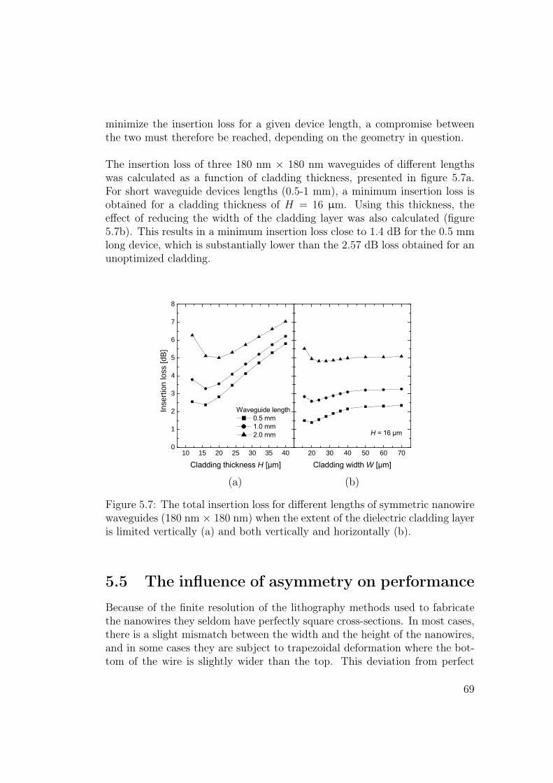
minimize the insertion loss for a given device length, a compromise betweenthe two must therefore be reached, depending on the geometry in question.
The insertion loss of three 180 nm × 180 nm waveguides of different lengthswas calculated as a function of cladding thickness, presented in figure 5.7a.For short waveguide devices lengths (0.5-1 mm), a minimum insertion loss isobtained for a cladding thickness of H = 16 µm. Using this thickness, theeffect of reducing the width of the cladding layer was also calculated (figure5.7b). This results in a minimum insertion loss close to 1.4 dB for the 0.5 mmlong device, which is substantially lower than the 2.57 dB loss obtained for anunoptimized cladding.
1 0 1 5 2 0 2 5 3 0 3 5 4 00
1
2
3
4
5
6
7
8
Insert
ion lo
ss [dB
]
�
� ����������������H �����
�����������������������������������
2 0 3 0 4 0 5 0 6 0 7 0
�
� ������������W �����
H ��������
(a) (b)
Figure 5.7: The total insertion loss for different lengths of symmetric nanowirewaveguides (180 nm × 180 nm) when the extent of the dielectric cladding layeris limited vertically (a) and both vertically and horizontally (b).
5.5 The influence of asymmetry on performanceBecause of the finite resolution of the lithography methods used to fabricatethe nanowires they seldom have perfectly square cross-sections. In most cases,there is a slight mismatch between the width and the height of the nanowires,and in some cases they are subject to trapezoidal deformation where the bot-tom of the wire is slightly wider than the top. This deviation from perfect
69
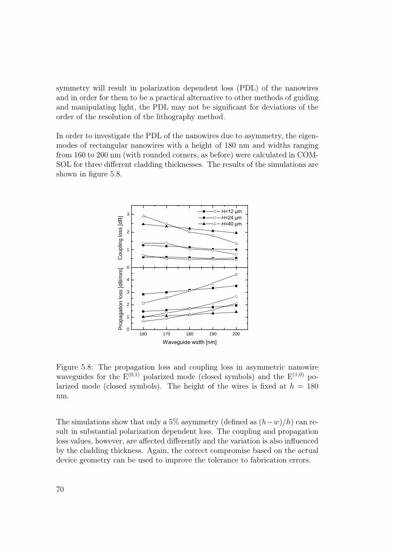
symmetry will result in polarization dependent loss (PDL) of the nanowiresand in order for them to be a practical alternative to other methods of guidingand manipulating light, the PDL may not be significant for deviations of theorder of the resolution of the lithography method.
In order to investigate the PDL of the nanowires due to asymmetry, the eigen-modes of rectangular nanowires with a height of 180 nm and widths rangingfrom 160 to 200 nm (with rounded corners, as before) were calculated in COM-SOL for three different cladding thicknesses. The results of the simulations areshown in figure 5.8.
1 6 0 1 7 0 1 8 0 1 9 0 2 0 00
1
2
3
4
0
1
2
3
�
Propa
gatio
n los
s [dB
/mm]
��� ��������������
�H ��� ���H ��������H ������
�
Coup
ling lo
ss [dB
]
Figure 5.8: The propagation loss and coupling loss in asymmetric nanowirewaveguides for the E(0,1) polarized mode (closed symbols) and the E(1,0) po-larized mode (closed symbols). The height of the wires is fixed at h = 180nm.
The simulations show that only a 5% asymmetry (defined as (h−w)/h) can re-sult in substantial polarization dependent loss. The coupling and propagationloss values, however, are affected differently and the variation is also influencedby the cladding thickness. Again, the correct compromise based on the actualdevice geometry can be used to improve the tolerance to fabrication errors.
70
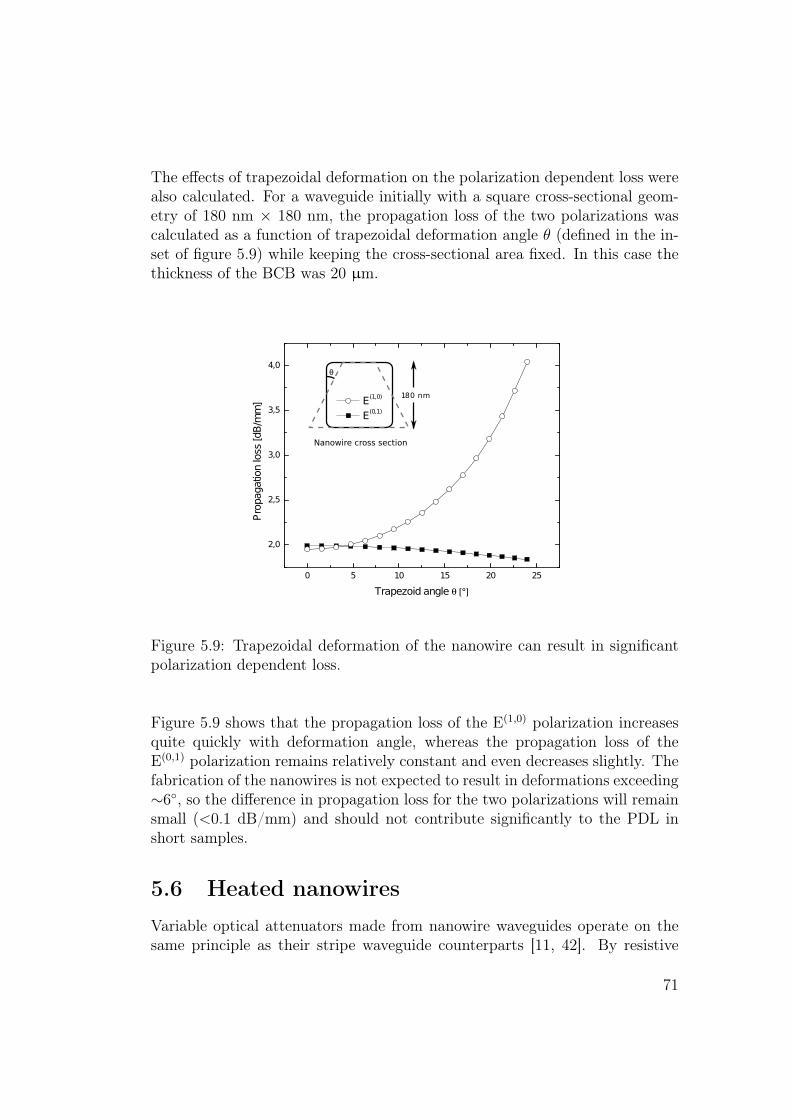
The effects of trapezoidal deformation on the polarization dependent loss werealso calculated. For a waveguide initially with a square cross-sectional geom-etry of 180 nm × 180 nm, the propagation loss of the two polarizations wascalculated as a function of trapezoidal deformation angle θ (defined in the in-set of figure 5.9) while keeping the cross-sectional area fixed. In this case thethickness of the BCB was 20 µm.
0 5 10 15 20 25
2,0
2,5
3,0
3,5
4,0
Pro
paga
tion
loss
[dB
/mm
]
Trapezoid angle θ [°]
E(1,0)
E(0,1)
180 nm
θ
Nanowire cross section
Figure 5.9: Trapezoidal deformation of the nanowire can result in significantpolarization dependent loss.
Figure 5.9 shows that the propagation loss of the E(1,0) polarization increasesquite quickly with deformation angle, whereas the propagation loss of theE(0,1) polarization remains relatively constant and even decreases slightly. Thefabrication of the nanowires is not expected to result in deformations exceeding∼6◦, so the difference in propagation loss for the two polarizations will remainsmall (<0.1 dB/mm) and should not contribute significantly to the PDL inshort samples.
5.6 Heated nanowiresVariable optical attenuators made from nanowire waveguides operate on thesame principle as their stripe waveguide counterparts [11, 42]. By resistive
71
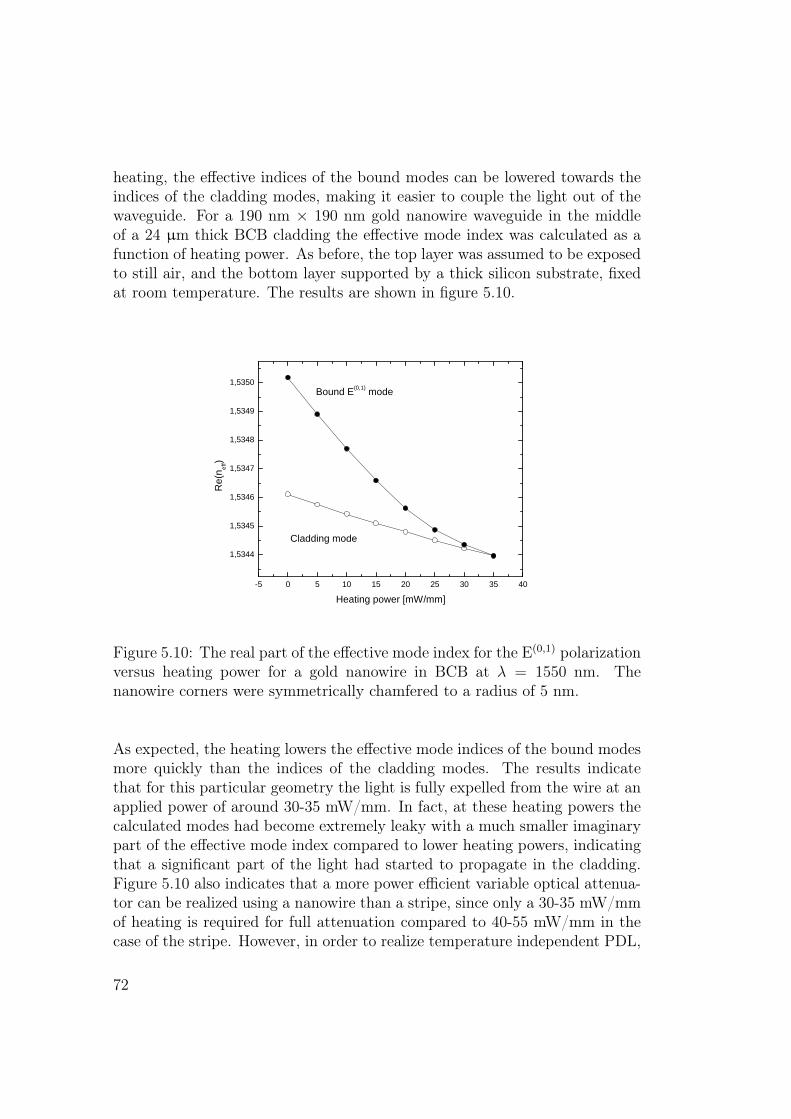
heating, the effective indices of the bound modes can be lowered towards theindices of the cladding modes, making it easier to couple the light out of thewaveguide. For a 190 nm × 190 nm gold nanowire waveguide in the middleof a 24 µm thick BCB cladding the effective mode index was calculated as afunction of heating power. As before, the top layer was assumed to be exposedto still air, and the bottom layer supported by a thick silicon substrate, fixedat room temperature. The results are shown in figure 5.10.
- 5 0 5 1 0 1 5 2 0 2 5 3 0 3 5 4 0
1 , 5 3 4 4
1 , 5 3 4 5
1 , 5 3 4 6
1 , 5 3 4 7
1 , 5 3 4 8
1 , 5 3 4 9
1 , 5 3 5 0
Re(n eff
)
H e a t i n g p o w e r [ m W / m m ]
C l a d d i n g m o d e
B o u n d E ( 0 , 1 ) m o d e
Figure 5.10: The real part of the effective mode index for the E(0,1) polarizationversus heating power for a gold nanowire in BCB at λ = 1550 nm. Thenanowire corners were symmetrically chamfered to a radius of 5 nm.
As expected, the heating lowers the effective mode indices of the bound modesmore quickly than the indices of the cladding modes. The results indicatethat for this particular geometry the light is fully expelled from the wire at anapplied power of around 30-35 mW/mm. In fact, at these heating powers thecalculated modes had become extremely leaky with a much smaller imaginarypart of the effective mode index compared to lower heating powers, indicatingthat a significant part of the light had started to propagate in the cladding.Figure 5.10 also indicates that a more power efficient variable optical attenua-tor can be realized using a nanowire than a stripe, since only a 30-35 mW/mmof heating is required for full attenuation compared to 40-55 mW/mm in thecase of the stripe. However, in order to realize temperature independent PDL,
72
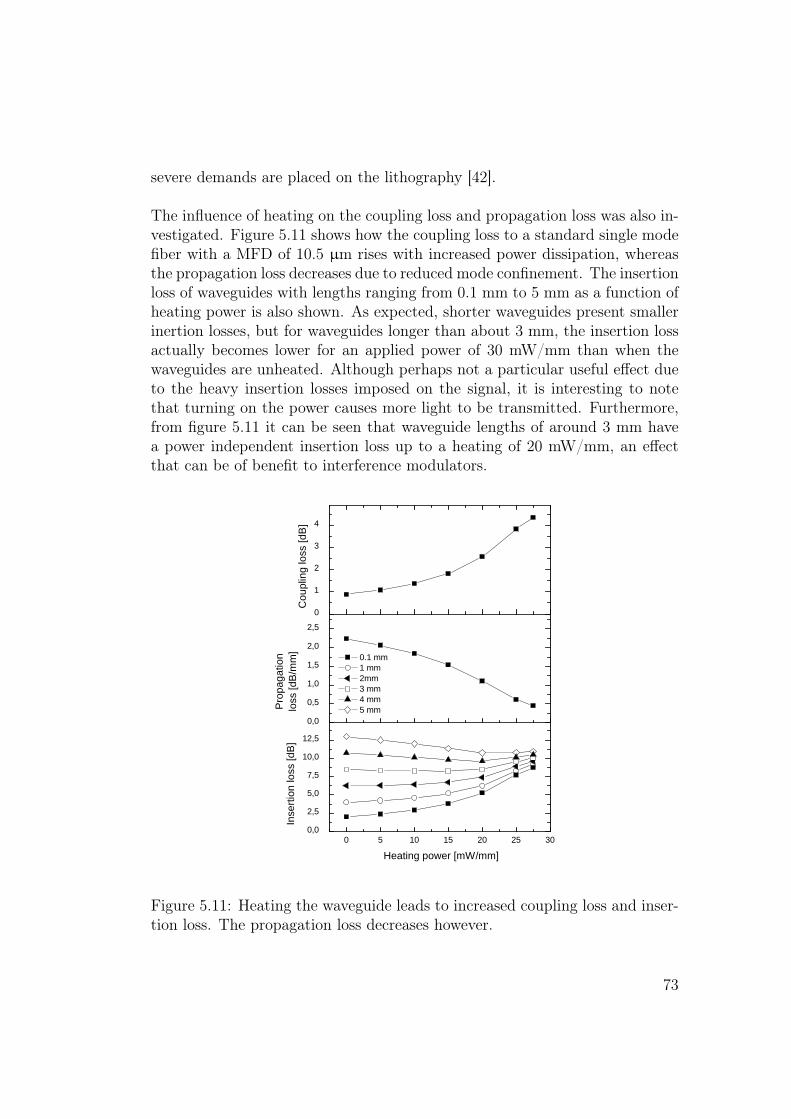
severe demands are placed on the lithography [42].
The influence of heating on the coupling loss and propagation loss was also in-vestigated. Figure 5.11 shows how the coupling loss to a standard single modefiber with a MFD of 10.5 µm rises with increased power dissipation, whereasthe propagation loss decreases due to reduced mode confinement. The insertionloss of waveguides with lengths ranging from 0.1 mm to 5 mm as a function ofheating power is also shown. As expected, shorter waveguides present smallerinertion losses, but for waveguides longer than about 3 mm, the insertion lossactually becomes lower for an applied power of 30 mW/mm than when thewaveguides are unheated. Although perhaps not a particular useful effect dueto the heavy insertion losses imposed on the signal, it is interesting to notethat turning on the power causes more light to be transmitted. Furthermore,from figure 5.11 it can be seen that waveguide lengths of around 3 mm havea power independent insertion loss up to a heating of 20 mW/mm, an effectthat can be of benefit to interference modulators.
0
1
2
3
4
Coup
ling lo
ss [dB
]
0 , 00 , 51 , 01 , 52 , 02 , 5
Propa
gatio
nlos
s [dB
/mm]
0 5 1 0 1 5 2 0 2 5 3 00 , 02 , 55 , 07 , 5
1 0 , 01 2 , 5
0 . 1 m m 1 m m 2 m m 3 m m 4 m m 5 m m
H e a t i n g p o w e r [ m W / m m ]
Insert
ion lo
ss [dB
]
Figure 5.11: Heating the waveguide leads to increased coupling loss and inser-tion loss. The propagation loss decreases however.
73

74
6 Conclusion and discussion
In this thesis the properties of long-range surface plasmon polariton (LR-SPP)stripe and nanowire waveguides and devices were investigated using the finiteelement method. By simultaneously using the stripes or wires as waveguidesand heating elements, the eigenmodes of the structures may be altered in orderto realize active waveguide components. Novel integrated optical devices basedon single-mode and multi-mode waveguides that have been presented experi-mentally in the literature have been analyzed in detail, such as variable opticalattenuators and directional couplers. Furthermore, a 1×2 optical switch basedon a multimode interferometer has been explored.
By optimizing the cross-sectional geometry of stripe waveguides with respectto insertion loss and coupling to a single mode fiber, a minimum insertionloss of 0.88 dB can be realized for a 1 mm long device at the telecommunica-tion wavelength λ = 1550 nm. In order for an actual device to approach thisvalue however, losses associated with the cladding polymer, scattering fromwaveguide imperfections, coupling to substrate and facet reflections must beminimized. Similarly, a considerably higher minimum insertion loss of 3.47dB was obtained for an equally long nanowire waveguide in an unoptimizedcladding. However, it was shown that the geometry of the cladding can havea substantial effect on the performance of nanowire waveguides. By correctlychoosing the cladding width and thickness, the insertion loss can be reducedto 2.57 dB.
The properties of heat transfer in LR-SPP waveguide components were in-vestigated with special emphasis on the mechanism of attenuation in variableoptical attenuators (VOAs). It was shown that by heating waveguides em-bedded in dielectric claddings with negative thermo-optic coefficients, the realpart of the effective mode index of bound modes is reduced. Due to the localnature of the heating, the effective mode indices of cladding modes drop moreslowly and LR-SPP waves are therefore more easily scattered into unboundmodes. The light in LR-SPP waveguides can therefore be attenuated simplyby passing a current through them, enabling the waveguides to be used asvariable optical attenuators.
In addition to VOAs, directional couplers and tunable multimode interfer-ence devices were also investigated. It was demonstrated that for a 40 µm
75
wide and 2.45 mm long MMI device consisting of two 4 µm wide electricallyisolated heating stripes on either side of a main body with an off-center inputwaveguide, switching between two output waveguides could be realized for anapplied power of 60 mW/mm.
Transient analysis of waveguide heating indicates that response times between1 and 2 ms can be expected for LR-SPP thermo-optic devices. It was revealedthat heating the waveguides under asymmetric cooling conditions increased thecoupling loss substantially, but reduced the propagation loss due to decreasedmode confinement. In the case of stripe waveguides, the waveguide length wasfound to play only a minor role in the overall insertion loss at heating currentsaround 50 mW/mm. Increasing the waveguide length by a factor of 100 (from0.1 mm to 10 mm) only increased the insertion loss by a modest 1.5 dB, in-dicating that efficient variable optical attenuators can be realized with shortwaveguide lengths. The same general behavior of the coupling loss and prop-agation loss with increased heating power was observed for nanowire waveg-uides, but the insertion loss of the different device lengths was not found toconverge as strongly as for the stripes in the heating range examined. Instead,other effects such as temperature independent insertion loss and insertion lossdecreasing with increased temperature, depending on device length, were seen.
The influence of waveguide asymmetry in the form of trapezoidal deformationor a mismatch between the waveguide width and height were also investigated.While the trapezoidal deformation was not found to contribute significantlyto polarization dependent loss in short samples for deformations within theexpected lithographic tolerances, only a 5% asymmetry between waveguidewidth and height was found to result in substantial polarization dependentloss.
Although the work presented here has focused on waveguides based on goldstripes or nanowires embedded in BCB, other metals and polymers can alsobe used. As mentioned before, BCB is chosen because of its simple processing,chemical resistance and relatively high glass transition temperature. By usinga polymer with a greater (i.e. more negative) thermo-optic coefficient, the ap-plied power necessary for attenuation or switching would be reduced, leadingto more power efficient devices and increased device lifetimes due to decreasedelectromigration. In addition to gold, silver also has suitable optical propertiesat telecommunication wavelengths [17], but is prone to oxidation which canrender it incapable of guiding SPPs.
76

As discussed earlier, the main drawbacks of LR-SPP stripe waveguides arethe strong polarization dependence and high loss. Even though the problemof polarization can be solved by replacing the stripe with a symmetric squarenanowire, the question of the short propagation distances remains. There iscurrently ongoing work which aims at reducing the propagation loss by plac-ing the waveguides in a gain medium and pulsing it with a laser, but thisis not expected to eradicate the loss completely. Keeping that in mind, LR-SPP technology is therefore mainly suited for simple, compact devices whilemore complex devices requiring longer propagation lengths, significant lateraldisplacements or multiple functionalities will in all cases exhibit excessive in-sertion loss compared to other available technologies that will in most casesoutweigh possible advantages.
77

78
Bibliography
[1] X. D. Hoa, A. G. Kirk and M. Tabrizian, Biosensors and Bioelectronics23, 151 (2007)
[2] S. M. Nie and S. R. Emery, Science 275, 1102 (1997)
[3] D. Sarid, Physical Review Letters 47, 1927 (1981)
[4] J. J. Burke, G. I. Stegeman, and T. Tamir, Physical Review B 33, 5186(1986)
[5] P. Berini, Physical Review B 61, 10484 (2000)
[6] R. Charbonneau, P. Berini, E. Berolo and E. Lisicka-Shrzek, Optics letters25, 844 (2000)
[7] T. Nikolajsen, K. Leosson, I. Salakhutdinov and S. I. Bozhevolnyi, AppliedPhysics Letters 82, 668 (2003)
[8] A. Boltasseva, T. Nikolajsen, K. Leosson, K. Kjaer, M. S. Larsen, and S.I. Bozhevolnyi, Journal of Lightwave Technology 23, 413 (2005)
[9] T. Nikolajsen and K. Leosson and S. I. Bozhevolnyi, Applied Physics Let-ters 85, 5833 (2004)
[10] P. Berini, US patent number 6,741,782 (2004)
[11] K. Leosson, T. Nikolajsen, A. Boltasseva and S. I. Bozhevolnyi, Opt.Express 14, 314 (2006)
[12] J. Jung, T. Søndergaard and S. I. Bozhevolnyi, Physical Review B 76,035434 (2007)
[13] The Dow Chemical Company, CYCLOTENE Advanced Electronics Resins- Properties, retrieved 31/10/2007,<http://www.dow.com/cyclotene/solution/index.htm>
79
[14] D. K. Cheng, Field and Wave Electromagnetics, 2nd edition (Addison-Wesley, New York, 1989)
[15] S. A. Maier, Plasmonics: Fundamentals and Applications (Springer,Berlin, 2007)
[16] N. W. Ashcroft and N. D. Mermin, Solid State Physics (Brooks Cole,1976)
[17] P. B. Johnson and R. W. Christy, Physical Review B 6, 4370 (1972)
[18] H. Raether, Surface Plasmons on Smooth and Rough Surfaces and onGratings (Springer, 1988)
[19] J. R. Sambles, G. W. Bradbery, and F. Yang, Contemporary Physics 32,173 (1991)
[20] J. R. Krenn, R. Wolf, A. Leitner and F. R. Aussenegg, Optics Communi-cations 137, 46 (1997)
[21] B. Hecht, H. Bielefeldt, L. Novotny, Y. Inouye and D. W. Pohl, PhysicalReview Letters 77, 1889 (1996)
[22] C. S. Desai and T. Kundu, Introductory Finite Element Method (CRCPress, 2001)
[23] G. P. Nikishkov, Introduction to the Finite Element Method, 2009 lecturenotes. University of Aizu, Japan, retrieved 25/02/2009,<http://www.u-aizu.ac.jp/ niki/feminstr/introfem/introfem.html>
[24] R. D. Cook, D. S. Malkus and M. E. Plesha, Concepts and Applicationsof Finite Element Analysis, 3rd edition (Wiley, New York, 1989)
[25] G. R. Liu and S. S. Quek, The Finite Element Method: A Practical Course(Butterworth-Heinemann, 2003)
[26] COMSOL AB, Sweden <www.comsol.com>
[27] Comsol Multiphysics, User’s guide for version 3.3
[28] P.L. George and H. Borouchaki, Delaunay Triangulation and Meshing(Hermes, Paris, 1998)
[29] The Engineering toolbox, Air Properties, retrieved 30/11/2007,<http://www.engineeringtoolbox.com/air-properties-d_156.html>
80
[30] eFunda, The thermal conductivity of gold, retrieved 30/11/2007,<http://www.efunda.com/materials/elements/TC_Table.cfm?Element_ID=Au>
[31] eFunda, The heat capacity of gold, retrieved 30/11/2007,<http://www.efunda.com/materials/elements/HC_Table.cfm?Element_ID=Au>
[32] A. Modafe, N. Ghalichechian, M. Powers, M. Khbeis and Reza Ghodssi,Microelectronic Engineering 82, 154 (2005)
[33] N.N. Smirnova, A.V. Markin, I.E. Boronina and M.A. Lopatin, Ther-mochimica Acta 433, 121 (2005)
[34] S. Guo, I. Lundstrom, and H. Arwin, Applied Physics Letters 68, 1910(1996)
[35] M. Rashidi-Huyeh and B. Palpant, Physical Review B 74, 075405 (2006)
[36] T. Nikolajsen, K. Leosson and S. I. Bozhevolnyi, Optics Communications244, 455 (2005)
[37] Enablence Technologies Inc., iVOA Integrated Variable Optical AttenuatorArray, retrieved 05/96/2009,<http://www.enablence.com/media/pdf/enablence_ivoa_datasheet.pdf>
[38] NeoPhotonics Corporation, FVOA5000 Compact Variable Optical Atten-uator, retrieved 05/96/2009,<www.neophotonics.com/product/fvoa5000v7.pdf>
[39] F. Ladoucer and J. D. Love, Silica-Based Buried Channel Waveguides andDevices (Chapman and Hall, 1996)
[40] L. B. Soldano and E. C. M. Pennings, Journal of Lightwave Technology13, 615 (1995)
[41] Photon Design Ltd., UK <http://www.photond.com/>
[42] K. Leosson, T. Rosenzveig, P. G. Hermannsson, and A. Boltasseva, Opt.Express 16, 15546 (2008)
81