Embed Size (px)
Citation preview
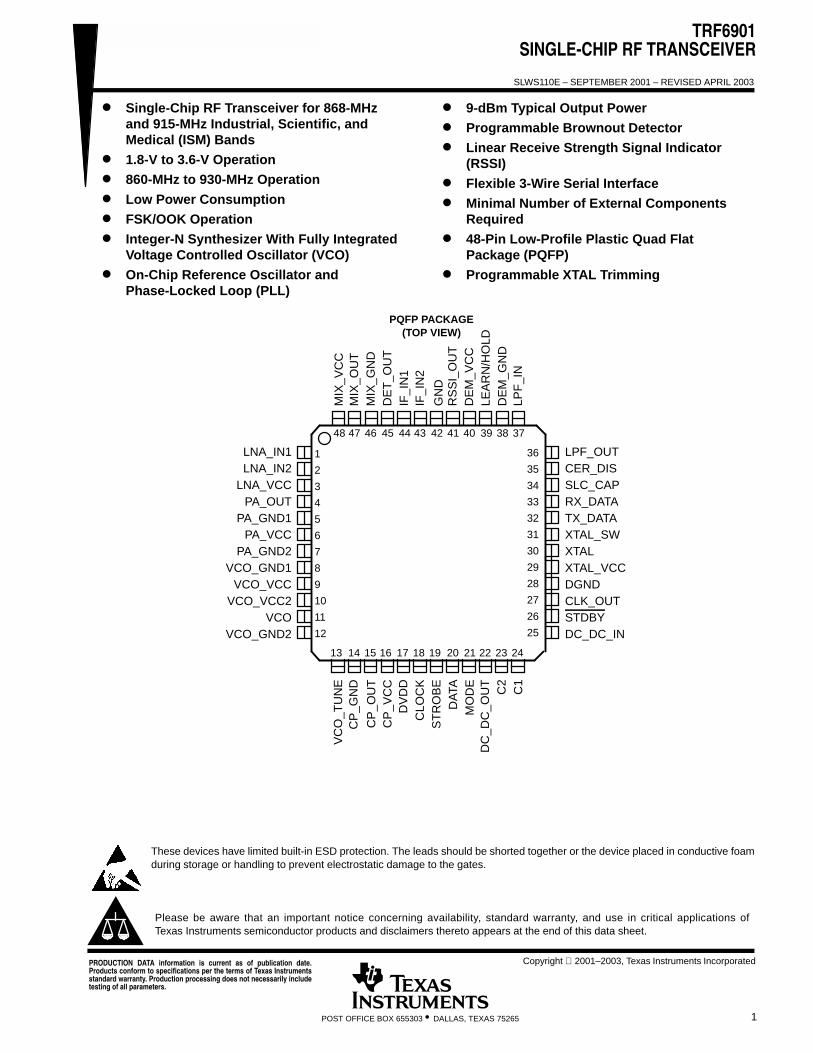
TRF6901SINGLE-CHIP RF TRANSCEIVER
SLWS110E – SEPTEMBER 2001 – REVISED APRIL 2003
1POST OFFICE BOX 655303 • DALLAS, TEXAS 75265
Single-Chip RF Transceiver for 868-MHzand 915-MHz Industrial, Scientific, andMedical (ISM) Bands
1.8-V to 3.6-V Operation
860-MHz to 930-MHz Operation
Low Power Consumption
FSK/OOK Operation
Integer-N Synthesizer With Fully IntegratedVoltage Controlled Oscillator (VCO)
On-Chip Reference Oscillator andPhase-Locked Loop (PLL)
9-dBm Typical Output Power
Programmable Brownout Detector
Linear Receive Strength Signal Indicator(RSSI)
Flexible 3-Wire Serial Interface
Minimal Number of External ComponentsRequired
48-Pin Low-Profile Plastic Quad FlatPackage (PQFP)
Programmable XTAL Trimming
14 15
36
35
34
33
32
31
30
29
28
27
26
25
16
1
2
3
4
5
6
7
8
9
10
11
12
17 18 19 20
RS
SI_
OU
TD
EM
_VC
CLE
AR
N/H
OLD
DE
M_G
ND
47 46 45 44 4348 42
MIX
_VC
CM
IX_O
UT
MIX
_GN
DD
ET
_OU
TIF
_IN
1
DC
_DC
_OU
TC
2C
1
CP
_OU
T
DV
DD
CLO
CK
ST
RO
BE
DA
TAM
OD
E
40 39 3841
21 22 23 24
37
13
LPF
_IN
IF_I
N2
GN
D
CP
_GN
DV
CO
_TU
NE
CP
_VC
C
PQFP PACKAGE(TOP VIEW)
LNA_IN1LNA_IN2
LNA_VCCPA_OUT
PA_GND1PA_VCC
PA_GND2VCO_GND1
VCO_VCCVCO_VCC2
VCOVCO_GND2
LPF_OUTCER_DISSLC_CAPRX_DATATX_DATAXTAL_SWXTALXTAL_VCCDGNDCLK_OUTSTDBYDC_DC_IN
These devices have limited built-in ESD protection. The leads should be shorted together or the device placed in conductive foamduring storage or handling to prevent electrostatic damage to the gates.
PRODUCTION DATA information is current as of publication date.Products conform to specifications per the terms of Texas Instrumentsstandard warranty. Production processing does not necessarily includetesting of all parameters.
Copyright 2001–2003, Texas Instruments Incorporated
Please be aware that an important notice concerning availability, standard warranty, and use in critical applications ofTexas Instruments semiconductor products and disclaimers thereto appears at the end of this data sheet.
TRF6901SINGLE-CHIP RF TRANSCEIVER
SLWS110E – SEPTEMBER 2001 – REVISED APRIL 2003
2 POST OFFICE BOX 655303 • DALLAS, TEXAS 75265
description
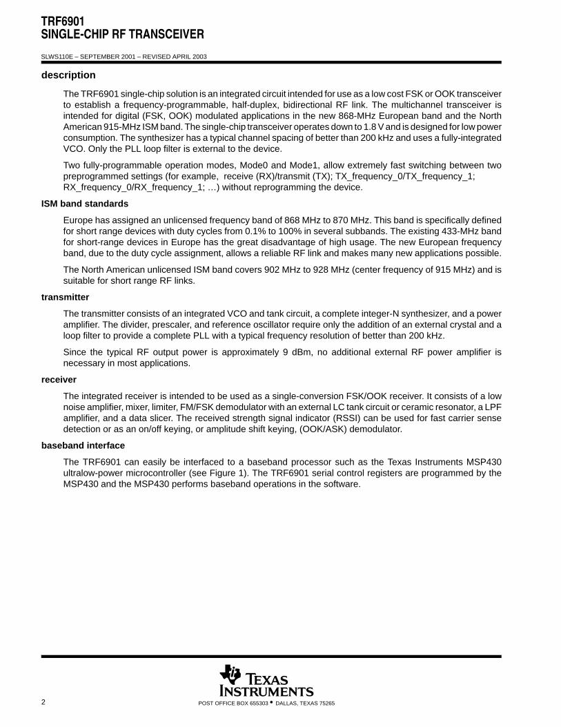
The TRF6901 single-chip solution is an integrated circuit intended for use as a low cost FSK or OOK transceiverto establish a frequency-programmable, half-duplex, bidirectional RF link. The multichannel transceiver isintended for digital (FSK, OOK) modulated applications in the new 868-MHz European band and the NorthAmerican 915-MHz ISM band. The single-chip transceiver operates down to 1.8 V and is designed for low powerconsumption. The synthesizer has a typical channel spacing of better than 200 kHz and uses a fully-integratedVCO. Only the PLL loop filter is external to the device.
Two fully-programmable operation modes, Mode0 and Mode1, allow extremely fast switching between twopreprogrammed settings (for example, receive (RX)/transmit (TX); TX_frequency_0/TX_frequency_1; RX_frequency_0/RX_frequency_1; …) without reprogramming the device.
ISM band standards
Europe has assigned an unlicensed frequency band of 868 MHz to 870 MHz. This band is specifically definedfor short range devices with duty cycles from 0.1% to 100% in several subbands. The existing 433-MHz bandfor short-range devices in Europe has the great disadvantage of high usage. The new European frequencyband, due to the duty cycle assignment, allows a reliable RF link and makes many new applications possible.
The North American unlicensed ISM band covers 902 MHz to 928 MHz (center frequency of 915 MHz) and issuitable for short range RF links.
transmitter
The transmitter consists of an integrated VCO and tank circuit, a complete integer-N synthesizer, and a poweramplifier. The divider, prescaler, and reference oscillator require only the addition of an external crystal and aloop filter to provide a complete PLL with a typical frequency resolution of better than 200 kHz.
Since the typical RF output power is approximately 9 dBm, no additional external RF power amplifier isnecessary in most applications.
receiver
The integrated receiver is intended to be used as a single-conversion FSK/OOK receiver. It consists of a lownoise amplifier, mixer, limiter, FM/FSK demodulator with an external LC tank circuit or ceramic resonator, a LPFamplifier, and a data slicer. The received strength signal indicator (RSSI) can be used for fast carrier sensedetection or as an on/off keying, or amplitude shift keying, (OOK/ASK) demodulator.
baseband interface
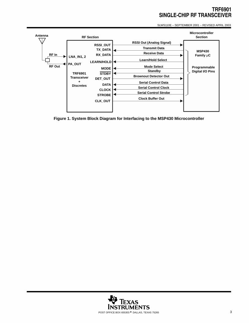
The TRF6901 can easily be interfaced to a baseband processor such as the Texas Instruments MSP430ultralow-power microcontroller (see Figure 1). The TRF6901 serial control registers are programmed by theMSP430 and the MSP430 performs baseband operations in the software.
TRF6901SINGLE-CHIP RF TRANSCEIVER
SLWS110E – SEPTEMBER 2001 – REVISED APRIL 2003
3POST OFFICE BOX 655303 • DALLAS, TEXAS 75265
Transmit Data
Receive Data
Mode Select
Serial Control Data
Serial Control Clock
Serial Control Strobe
TX_DATA
RX_DATA
MODE
STDBY
DATA
CLOCK
STROBE
LNA_IN1, 2
PA_OUT
TRF6901Transceiver
+Discretes
RF Section
ProgrammableDigital I/O Pins
MSP430Family µC
MicrocontrollerSectionAntenna
Standby
RF In
RF Out
RSSI Out (Analog Signal)RSSI_OUT
Clock Buffer OutCLK_OUT
Brownout Detector OutDET_OUT
Learn/Hold SelectLEARN/HOLD
Figure 1. System Block Diagram for Interfacing to the MSP430 Microcontroller
TRF6901SINGLE-CHIP RF TRANSCEIVER
SLWS110E – SEPTEMBER 2001 – REVISED APRIL 2003
4 POST OFFICE BOX 655303 • DALLAS, TEXAS 75265
functional block diagram
PA_OUT
CeramicDiscriminator
SerialInterface
LNA
CLK_OUT
CLOCKDATASTROBE
PA
TX_DATA
Band-gap
/N
/A-Counter
Loop Filter
Limiter
QuadratureDemodulator
RX_DATA
LPF Amplifier
Data Slicer
CeramicIF Filter
BrownoutMODE
85
/L
8
/Div. CTRL8
6
RSSI RSSI_OUT
860 MHz to 930 MHztypical 9 dBm
DC-DCConverter
PFDCPs /Ref
/K
/B-
RFIN
DC_DC_IN
Counter
2..2542..62
Detector
VCO
33
41
1820192621
32
DET_OUT45
860 MHz to 930 MHz
LNA_IN1, LNA_IN2
DC_DC_OUT
25
22
4
32/33
1, 2
30 31
CE
R_D
IS
LP
F_I
N
LP
F_O
UT
IF_I
N1,
2
MIX
_OU
T
XTA
L_S
W
LE
AR
N/H
OL
D
SL
C_C
AP
XTA
L
47 44, 43 35 37 36 39 34
27
15 CP_OUT13VCO_TUNE
2..255
Mixer
STDBY
10.7-MHz
Terminal FunctionsTERMINAL
I/O DESCRIPTIONNAME NO.
I/O DESCRIPTION
C1 24 Connect to external capacitor for operation of dc-dc converter
C2 23 Connect to external capacitor for operation of dc-dc converter
CER_DIS 35 Connect to external ceramic discriminator
CLK_OUT 27 O Clock signal output for connection to external microcontroller
CLOCK 18 I Serial interface clock signal input
CP_GND 14 Charge pump ground
CP_OUT 15 O Charge pump output
CP_VCC 16 I Charge pump input VCC from dc-dc converter
DATA 20 I Serial interface data signal input
TRF6901SINGLE-CHIP RF TRANSCEIVER
SLWS110E – SEPTEMBER 2001 – REVISED APRIL 2003
5POST OFFICE BOX 655303 • DALLAS, TEXAS 75265
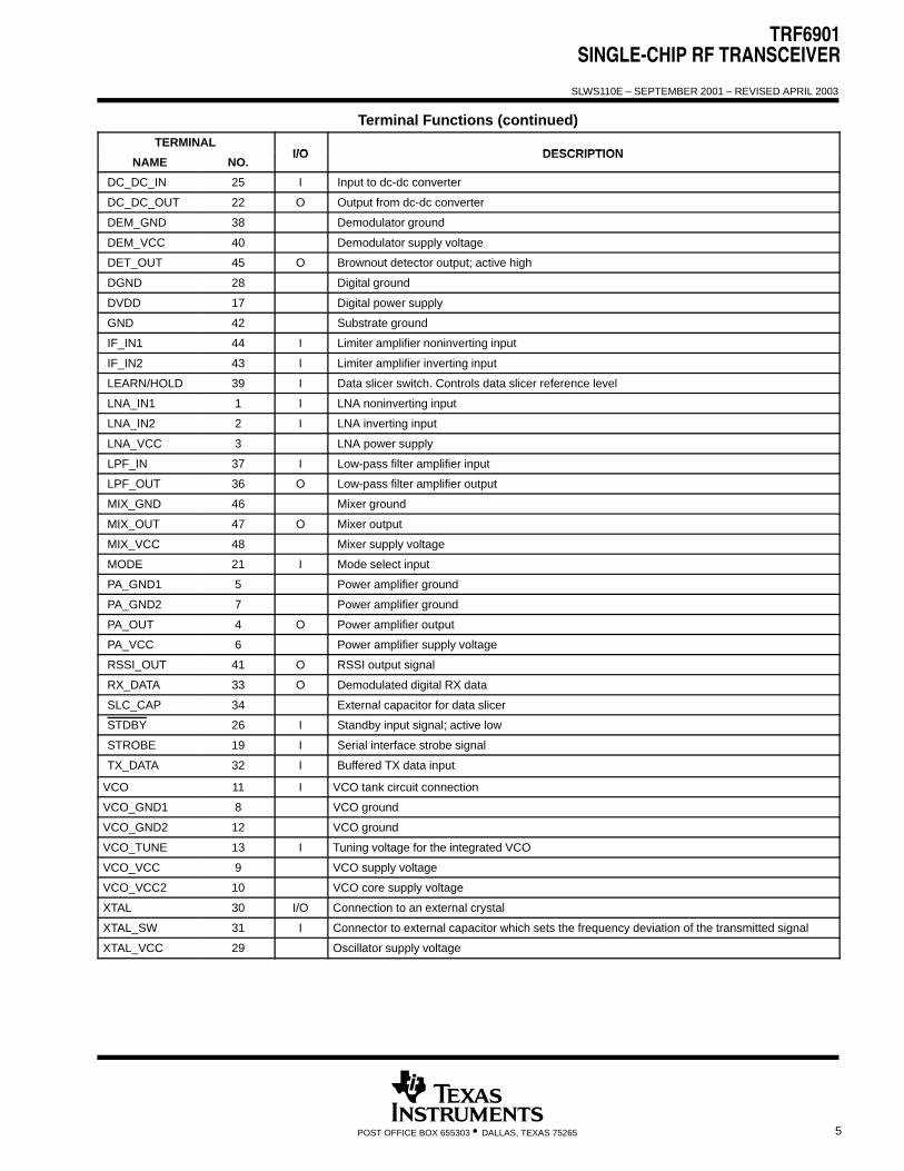
Terminal Functions (continued)TERMINAL
I/O DESCRIPTIONNAME NO.
I/O DESCRIPTION
DC_DC_IN 25 I Input to dc-dc converter
DC_DC_OUT 22 O Output from dc-dc converter
DEM_GND 38 Demodulator ground
DEM_VCC 40 Demodulator supply voltage
DET_OUT 45 O Brownout detector output; active high
DGND 28 Digital ground
DVDD 17 Digital power supply
GND 42 Substrate ground
IF_IN1 44 I Limiter amplifier noninverting input
IF_IN2 43 I Limiter amplifier inverting input
LEARN/HOLD 39 I Data slicer switch. Controls data slicer reference level
LNA_IN1 1 I LNA noninverting input
LNA_IN2 2 I LNA inverting input
LNA_VCC 3 LNA power supply
LPF_IN 37 I Low-pass filter amplifier input
LPF_OUT 36 O Low-pass filter amplifier output
MIX_GND 46 Mixer ground
MIX_OUT 47 O Mixer output
MIX_VCC 48 Mixer supply voltage
MODE 21 I Mode select input
PA_GND1 5 Power amplifier ground
PA_GND2 7 Power amplifier ground
PA_OUT 4 O Power amplifier output
PA_VCC 6 Power amplifier supply voltage
RSSI_OUT 41 O RSSI output signal
RX_DATA 33 O Demodulated digital RX data
SLC_CAP 34 External capacitor for data slicer
STDBY 26 I Standby input signal; active low
STROBE 19 I Serial interface strobe signal
TX_DATA 32 I Buffered TX data input
VCO 11 I VCO tank circuit connection
VCO_GND1 8 VCO ground
VCO_GND2 12 VCO ground
VCO_TUNE 13 I Tuning voltage for the integrated VCO
VCO_VCC 9 VCO supply voltage
VCO_VCC2 10 VCO core supply voltage
XTAL 30 I/O Connection to an external crystal
XTAL_SW 31 I Connector to external capacitor which sets the frequency deviation of the transmitted signal
XTAL_VCC 29 Oscillator supply voltage
TRF6901SINGLE-CHIP RF TRANSCEIVER
SLWS110E – SEPTEMBER 2001 – REVISED APRIL 2003
6 POST OFFICE BOX 655303 • DALLAS, TEXAS 75265
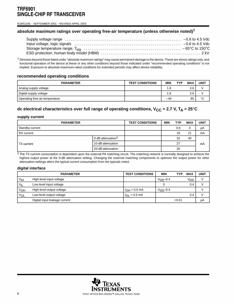
absolute maximum ratings over operating free-air temperature (unless otherwise noted)†
Supply voltage range –0.6 to 4.5 Vdc. . . . . . . . . . . . . . . . . . . . . . . . . . . . . . . . . . . . . . . . . . . . . . . . . . . . . . . . . . . . . Input voltage, logic signals –0.6 to 4.5 Vdc. . . . . . . . . . . . . . . . . . . . . . . . . . . . . . . . . . . . . . . . . . . . . . . . . . . . . . . . Storage temperature range, Tstg – 65°C to 150°C. . . . . . . . . . . . . . . . . . . . . . . . . . . . . . . . . . . . . . . . . . . . . . . . . . . ESD protection, human body model (HBM) 2 kV. . . . . . . . . . . . . . . . . . . . . . . . . . . . . . . . . . . . . . . . . . . . . . . . . . . .
† Stresses beyond those listed under “absolute maximum ratings” may cause permanent damage to the device. These are stress ratings only, andfunctional operation of the device at these or any other conditions beyond those indicated under “recommended operating conditions” is notimplied. Exposure to absolute-maximum-rated conditions for extended periods may affect device reliability.
recommended operating conditions
PARAMETER TEST CONDITIONS MIN TYP MAX UNIT
Analog supply voltage 1.8 3.6 V
Digital supply voltage 1.8 3.6 V
Operating free-air temperature –40 85 °C
dc electrical characteristics over full range of operating conditions, VCC = 2.7 V, TA = 25°C
supply currentPARAMETER TEST CONDITIONS MIN TYP MAX UNIT
Standby current 0.6 4 µA
RX current 18 21 mA
0-dB attenuation‡ 32 40
TX current 10-dB attenuation 27 mATX current
20-dB attenuation 26
mA
‡ The TX current consumption is dependent upon the external PA matching circuit. The matching network is normally designed to achieve thehighest output power at the 0-dB attenuation setting. Changing the external matching components to optimize the output power for otherattenuation settings alters the typical current consumption from the typicals noted.
digital interfacePARAMETER TEST CONDITIONS MIN TYP MAX UNIT
VIH High-level input voltage VDD–0.4 VDD V
VIL Low-level input voltage 0 0.4 V
VOH High-level output voltage IOH = 0.5 mA VDD–0.4 V
VOL Low-level output voltage IOL = 0.5 mA 0.4 V
Digital input leakage current <0.01 µA
TRF6901SINGLE-CHIP RF TRANSCEIVER
SLWS110E – SEPTEMBER 2001 – REVISED APRIL 2003
7POST OFFICE BOX 655303 • DALLAS, TEXAS 75265
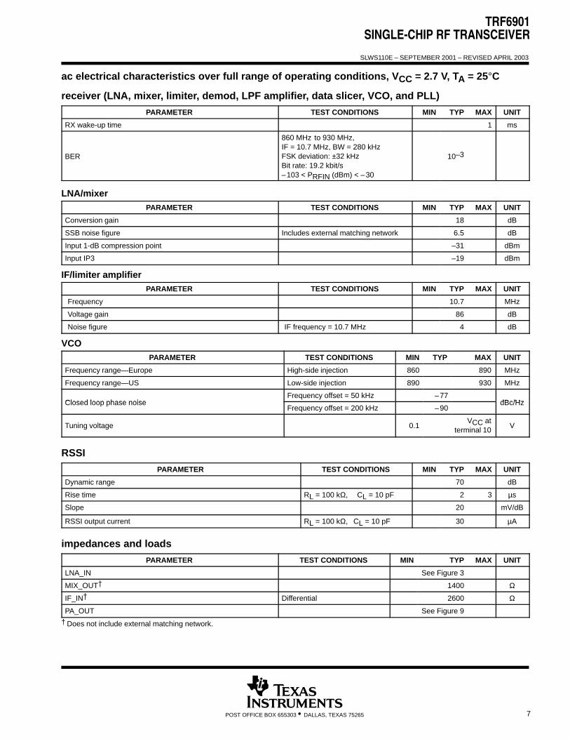
ac electrical characteristics over full range of operating conditions, VCC = 2.7 V, TA = 25°C
receiver (LNA, mixer, limiter, demod, LPF amplifier, data slicer, VCO, and PLL)
PARAMETER TEST CONDITIONS MIN TYP MAX UNIT
RX wake-up time 1 ms
BER
860 MHz to 930 MHz,IF = 10.7 MHz, BW = 280 kHzFSK deviation: ±32 kHzBit rate: 19.2 kbit/s –103 < PRFIN (dBm) < –30
10–3
LNA/mixerPARAMETER TEST CONDITIONS MIN TYP MAX UNIT
Conversion gain 18 dB
SSB noise figure Includes external matching network 6.5 dB
Input 1-dB compression point –31 dBm
Input IP3 –19 dBm
IF/limiter amplifierPARAMETER TEST CONDITIONS MIN TYP MAX UNIT
Frequency 10.7 MHz
Voltage gain 86 dB
Noise figure IF frequency = 10.7 MHz 4 dB
VCOPARAMETER TEST CONDITIONS MIN TYP MAX UNIT
Frequency range—Europe High-side injection 860 890 MHz
Frequency range—US Low-side injection 890 930 MHz
Closed loop phase noiseFrequency offset = 50 kHz –77
dBc/HzClosed loop phase noiseFrequency offset = 200 kHz –90
dBc/Hz
Tuning voltage 0.1VCC at
terminal 10V
RSSI
PARAMETER TEST CONDITIONS MIN TYP MAX UNIT
Dynamic range 70 dB
Rise time RL = 100 kΩ, CL = 10 pF 2 3 µs
Slope 20 mV/dB
RSSI output current RL = 100 kΩ, CL = 10 pF 30 µA
impedances and loads
PARAMETER TEST CONDITIONS MIN TYP MAX UNIT
LNA_IN See Figure 3
MIX_OUT 1400 Ω
IF_IN Differential 2600 Ω
PA_OUT See Figure 9
† Does not include external matching network.
TRF6901SINGLE-CHIP RF TRANSCEIVER
SLWS110E – SEPTEMBER 2001 – REVISED APRIL 2003
8 POST OFFICE BOX 655303 • DALLAS, TEXAS 75265
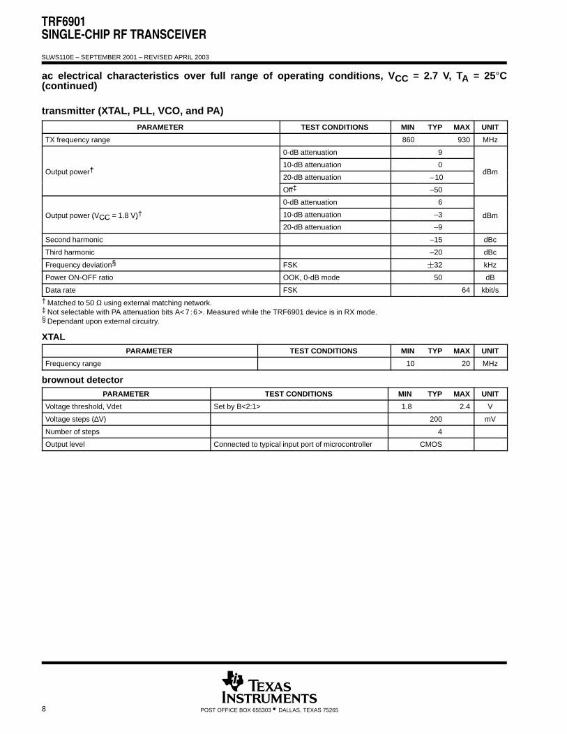
ac electrical characteristics over full range of operating conditions, VCC = 2.7 V, TA = 25°C(continued)
transmitter (XTAL, PLL, VCO, and PA)
PARAMETER TEST CONDITIONS MIN TYP MAX UNIT
TX frequency range 860 930 MHz
0-dB attenuation 9
Output power†10-dB attenuation 0
dBmOutput power†20-dB attenuation –10
dBm
Off‡ –50
0-dB attenuation 6
Output power (VCC = 1.8 V)† 10-dB attenuation –3 dBmOut ut ower (VCC 1.8 V)
20-dB attenuation –9
dBm
Second harmonic –15 dBc
Third harmonic –20 dBc
Frequency deviation§ FSK 32 kHz
Power ON-OFF ratio OOK, 0-dB mode 50 dB
Data rate FSK 64 kbit/s
† Matched to 50 Ω using external matching network.‡ Not selectable with PA attenuation bits A<7 :6>. Measured while the TRF6901 device is in RX mode.§ Dependant upon external circuitry.
XTALPARAMETER TEST CONDITIONS MIN TYP MAX UNIT
Frequency range 10 20 MHz
brownout detectorPARAMETER TEST CONDITIONS MIN TYP MAX UNIT
Voltage threshold, Vdet Set by B<2:1> 1.8 2.4 V
Voltage steps (∆V) 200 mV
Number of steps 4
Output level Connected to typical input port of microcontroller CMOS
TRF6901SINGLE-CHIP RF TRANSCEIVER
SLWS110E – SEPTEMBER 2001 – REVISED APRIL 2003
9POST OFFICE BOX 655303 • DALLAS, TEXAS 75265
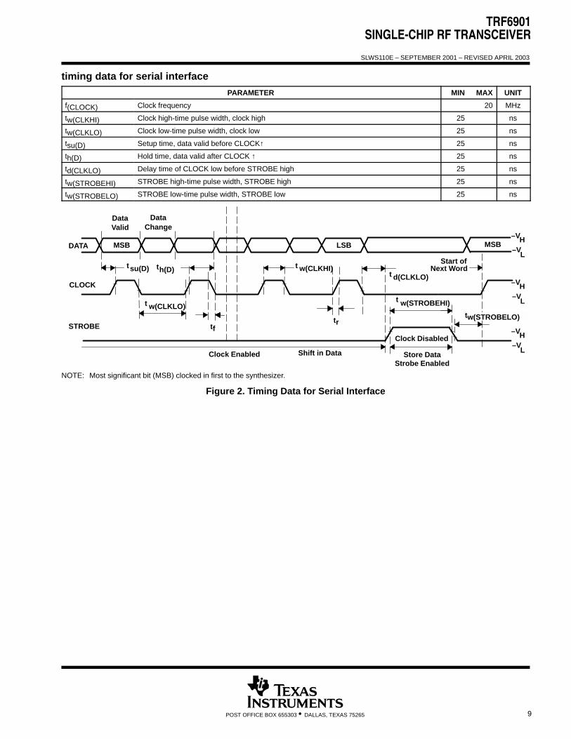
timing data for serial interface
PARAMETER MIN MAX UNIT
f(CLOCK) Clock frequency 20 MHz
tw(CLKHI) Clock high-time pulse width, clock high 25 ns
tw(CLKLO) Clock low-time pulse width, clock low 25 ns
tsu(D) Setup time, data valid before CLOCK↑ 25 ns
th(D) Hold time, data valid after CLOCK ↑ 25 ns
td(CLKLO) Delay time of CLOCK low before STROBE high 25 ns
tw(STROBEHI) STROBE high-time pulse width, STROBE high 25 ns
tw(STROBELO) STROBE low-time pulse width, STROBE low 25 ns
STROBE
tsu(D)
DataValid
DataChange
DATA
CLOCK
th(D) t w(CLKHI)
t w(CLKLO)
Clock Disabled
Store DataShift in Data
t w(STROBEHI)
–VH–V
L
t d(CLKLO)
MSB LSB MSB
Start ofNext Word
Strobe EnabledClock Enabled
–VH–V
L
–VH–V
L
tw(STROBELO)tf
tr
NOTE: Most significant bit (MSB) clocked in first to the synthesizer.
Figure 2. Timing Data for Serial Interface
TRF6901SINGLE-CHIP RF TRANSCEIVER
SLWS110E – SEPTEMBER 2001 – REVISED APRIL 2003
10 POST OFFICE BOX 655303 • DALLAS, TEXAS 75265
detailed description
low-noise amplifier (LNA)/RF mixer
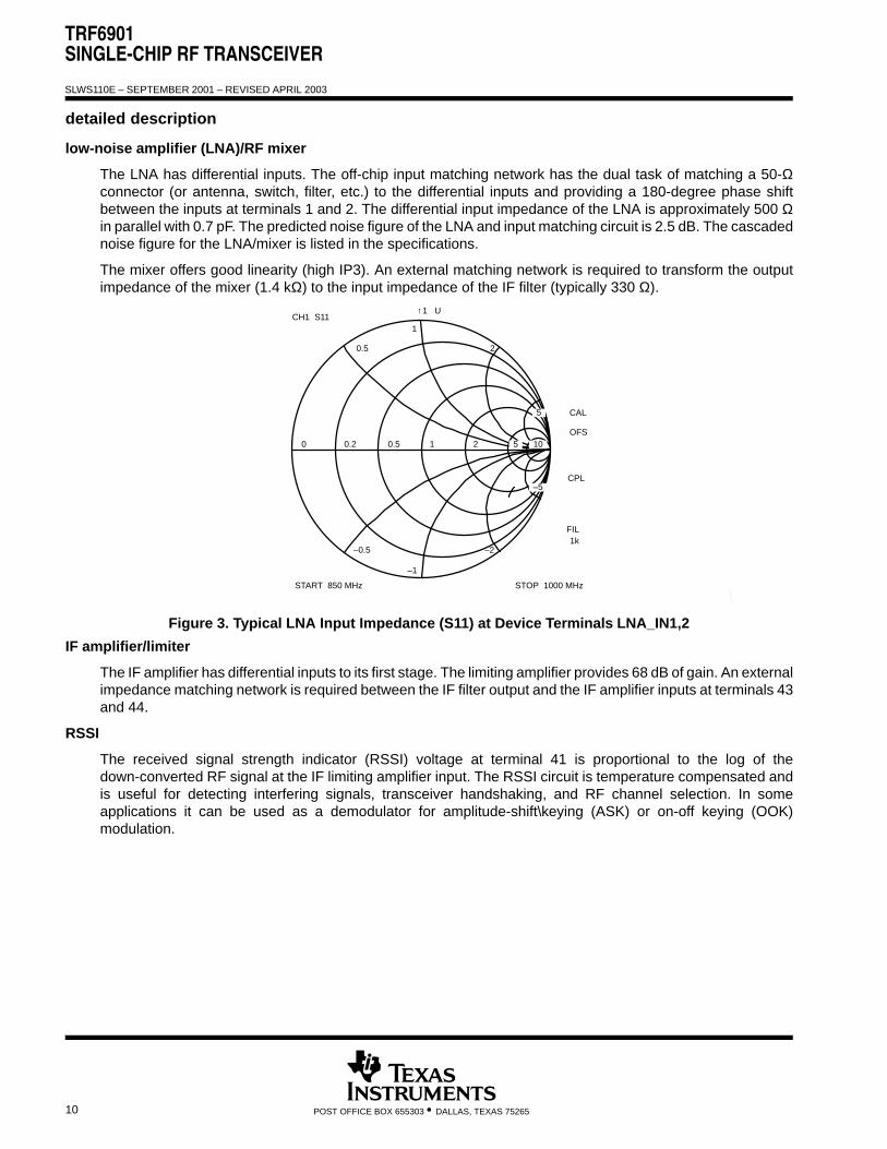
The LNA has differential inputs. The off-chip input matching network has the dual task of matching a 50-Ωconnector (or antenna, switch, filter, etc.) to the differential inputs and providing a 180-degree phase shiftbetween the inputs at terminals 1 and 2. The differential input impedance of the LNA is approximately 500 Ωin parallel with 0.7 pF. The predicted noise figure of the LNA and input matching circuit is 2.5 dB. The cascadednoise figure for the LNA/mixer is listed in the specifications.
The mixer offers good linearity (high IP3). An external matching network is required to transform the outputimpedance of the mixer (1.4 kΩ) to the input impedance of the IF filter (typically 330 Ω).
0.5
1
2
5
10210.50.20
–0.5
–1
–2
–5
5
↑1 U
START 850 MHz STOP 1000 MHz
CH1 S11
CAL
OFS
CPL
FIL1k
Figure 3. Typical LNA Input Impedance (S11) at Device Terminals LNA_IN1,2
IF amplifier/limiter
The IF amplifier has differential inputs to its first stage. The limiting amplifier provides 68 dB of gain. An externalimpedance matching network is required between the IF filter output and the IF amplifier inputs at terminals 43and 44.
RSSI
The received signal strength indicator (RSSI) voltage at terminal 41 is proportional to the log of thedown-converted RF signal at the IF limiting amplifier input. The RSSI circuit is temperature compensated andis useful for detecting interfering signals, transceiver handshaking, and RF channel selection. In someapplications it can be used as a demodulator for amplitude-shift\keying (ASK) or on-off keying (OOK)modulation.
TRF6901SINGLE-CHIP RF TRANSCEIVER
SLWS110E – SEPTEMBER 2001 – REVISED APRIL 2003
11POST OFFICE BOX 655303 • DALLAS, TEXAS 75265
detailed description (continued)
demodulator
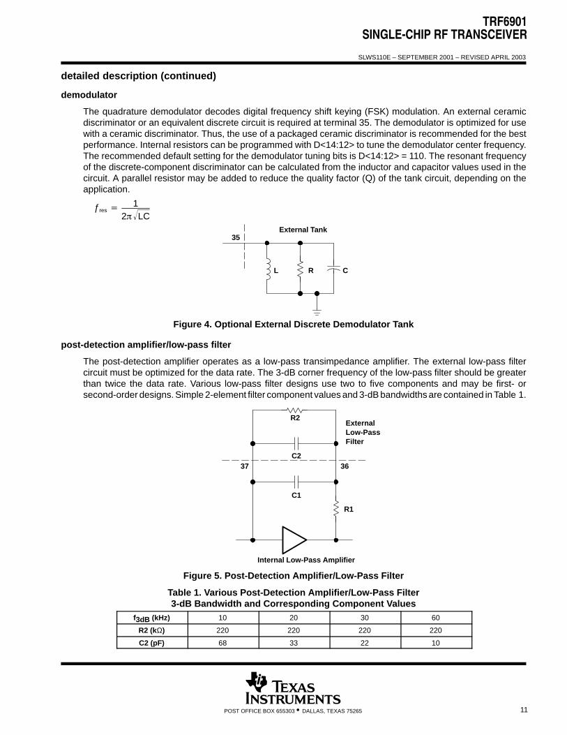
The quadrature demodulator decodes digital frequency shift keying (FSK) modulation. An external ceramicdiscriminator or an equivalent discrete circuit is required at terminal 35. The demodulator is optimized for usewith a ceramic discriminator. Thus, the use of a packaged ceramic discriminator is recommended for the bestperformance. Internal resistors can be programmed with D<14:12> to tune the demodulator center frequency.The recommended default setting for the demodulator tuning bits is D<14:12> = 110. The resonant frequencyof the discrete-component discriminator can be calculated from the inductor and capacitor values used in thecircuit. A parallel resistor may be added to reduce the quality factor (Q) of the tank circuit, depending on theapplication.
ƒres 1
2 LC
35
L R C
External Tank
Figure 4. Optional External Discrete Demodulator Tank
post-detection amplifier/low-pass filter
The post-detection amplifier operates as a low-pass transimpedance amplifier. The external low-pass filtercircuit must be optimized for the data rate. The 3-dB corner frequency of the low-pass filter should be greaterthan twice the data rate. Various low-pass filter designs use two to five components and may be first- orsecond-order designs. Simple 2-element filter component values and 3-dB bandwidths are contained in Table 1.
Internal Low-Pass Amplifier
37 36
ExternalLow-PassFilter
R1
C1
C2
R2
Figure 5. Post-Detection Amplifier/Low-Pass Filter
Table 1. Various Post-Detection Amplifier/Low-Pass Filter3-dB Bandwidth and Corresponding Component Values
f3dB (kHz) 10 20 30 60
R2 (kΩ) 220 220 220 220
C2 (pF) 68 33 22 10
TRF6901SINGLE-CHIP RF TRANSCEIVER
SLWS110E – SEPTEMBER 2001 – REVISED APRIL 2003
12 POST OFFICE BOX 655303 • DALLAS, TEXAS 75265
detailed description (continued)
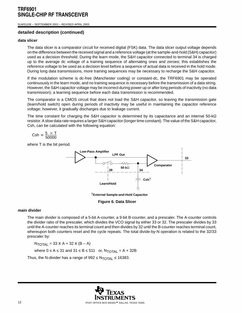
data slicer
The data slicer is a comparator circuit for received digital (FSK) data. The data slicer output voltage dependson the difference between the received signal and a reference voltage (at the sample-and-hold (S&H) capacitor)used as a decision threshold. During the learn mode, the S&H capacitor connected to terminal 34 is chargedup to the average dc voltage of a training sequence of alternating ones and zeroes; this establishes thereference voltage to be used as a decision level before a sequence of actual data is received in the hold mode.During long data transmissions, more training sequences may be necessary to recharge the S&H capacitor.
If the modulation scheme is dc-free (Manchester coding) or constant-dc, the TRF6901 may be operatedcontinuously in the learn mode, and no training sequence is necessary before the transmission of a data string.However, the S&H capacitor voltage may be incorrect during power up or after long periods of inactivity (no datatransmission); a learning sequence before each data transmission is recommended.
The comparator is a CMOS circuit that does not load the S&H capacitor, so leaving the transmission gate(learn/hold switch) open during periods of inactivity may be useful in maintaining the capacitor referencevoltage; however, it gradually discharges due to leakage current.
The time constant for charging the S&H capacitor is determined by its capacitance and an internal 50-kΩresistor. A slow data rate requires a larger S&H capacitor (longer time constant). The value of the S&H capacitor,Csh, can be calculated with the following equation:
Csh 5 T50000
where T is the bit period.
Low-Pass Amplifier
Csh
Learn/Hold
50 kΩ34
LPF Out
Comparator
39
External Sample-and-Hold Capacitor
33
Figure 6. Data Slicer
main divider
The main divider is composed of a 5-bit A-counter, a 9-bit B-counter, and a prescaler. The A-counter controlsthe divider ratio of the prescaler, which divides the VCO signal by either 33 or 32. The prescaler divides by 33until the A-counter reaches its terminal count and then divides by 32 until the B-counter reaches terminal count,whereupon both counters reset and the cycle repeats. The total divide-by-N operation is related to the 32/33prescaler by:
NTOTAL = 33 x A + 32 x (B – A)
where 0 ≤ A ≤ 31 and 31 ≤ B ≤ 511 or, NTOTAL = A + 32B
Thus, the N-divider has a range of 992 ≤ NTOTAL ≤ 16383.
TRF6901SINGLE-CHIP RF TRANSCEIVER
SLWS110E – SEPTEMBER 2001 – REVISED APRIL 2003
13POST OFFICE BOX 655303 • DALLAS, TEXAS 75265
detailed description (continued)
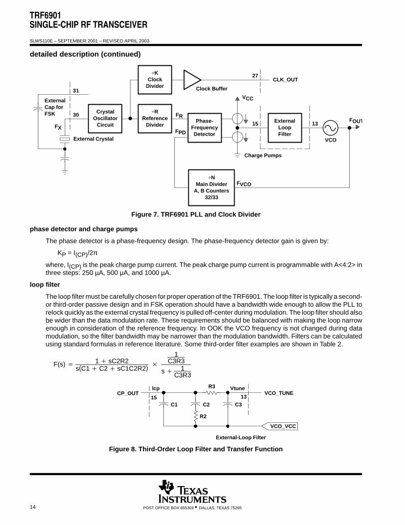
PLL
The phase-locked loop is the radio frequency synthesizer for the TRF6901. It is used to generate the transmitsignal and as the local oscillator for the receive mixer. The signal (FX) from a reference crystal oscillator (XO)is divided by an integer factor R down to FR. The minimum frequency resolution, and thus, the minimum channelspacing, is FR.
FR = FX ÷ R, where 1 ≤ R ≤ 256
The phase-locked loop is an integer-N design. The voltage-controlled oscillator (VCO) signal is divided by aninteger factor N to get a frequency at the phase detector input.
FPD = FVCO ÷ N, where FVCO = FOUT
The phase detector compares the divided VCO signal to the divided crystal frequency and implements an errorsignal from two charge pumps. The error signal corrects the VCO output to the desired frequency.
With FR = FPD under locked conditions, FOUT = FXN
R = (A + 32B) FR.
As is in any integer-N PLLs, the VCO output has spurs at integer multiples of the reference frequency (nFR).In applications requiring contiguous frequency channels, the reference frequency is often chosen to be equalto the channel spacing, thus, channel spacing = FR = FX ÷ R.
oscillator circuit and reference divider
The reference divider reduces the frequency of the external crystal (FX) by an 8-bit programmable integer divisorto an internal reference frequency (FR) used for the phase-locked loop. The choice of internal referencefrequency also has implications for lock time, maximum data rate, noise floor, and loop-filter design. The crystalfrequency can be tuned using the D word to control internal trimming capacitors, which are placed in parallelwith the crystal. These offset a small frequency error in the crystal. In an FSK application, an additional capacitoris placed in parallel (through terminal 31) with the external capacitor that is connected in series with the crystal,thus, changing the load capacitance as the transmit data switch (TX_DATA, terminal 32) is toggled. The changein load capacitance pulls the crystal off-frequency by the total frequency deviation.
Hence, the 2-FSK frequency set by the level of TX_DATA and the external capacitor, can be represented asfollows:
ƒout1 TX_DATA Low ƒout2 TX_DATA High
Note that the frequencies ƒout1 and ƒout2 are centered about the frequency ƒcenter = (ƒout1 + ƒout2)/2. Whentransmitting FSK, ƒcenter is considered to be the effective carrier frequency and any receiver local oscillator (LO)should be set to the same ƒcenter frequency ± the receiver’s IF frequency (ƒIF) for proper reception anddemodulation.
For the case of high-side injection, the receiver LO would be set to ƒLO = ƒcenter + ƒIF. Using high-side injection,the received data at terminal 33, RX_DATA, would be inverted from the transmitted data applied at terminal 32,TX_DATA. Conversely, for low-side injection, the receiver LO would be set to ƒLO = ƒcenter – ƒIF. Using low-sideinjection, the received data would be the same as the transmitted data.
In addition, when the TRF6901 is placed in receive mode, it is recommended that the TX_DATA terminal be keptlow. In this manner, the actual LO frequency injected into the mixer is ƒout1 = ƒLO. If TX_DATA is set high, thethe receiver LO would be offset, resulting in poor receiver sensitivity.
TRF6901SINGLE-CHIP RF TRANSCEIVER
SLWS110E – SEPTEMBER 2001 – REVISED APRIL 2003
14 POST OFFICE BOX 655303 • DALLAS, TEXAS 75265
detailed description (continued)
FX
CrystalOscillator
Circuit
31 Clock Buffer
External Crystal
ExternalCap forFSK ÷R
ReferenceDivider
÷KClock
Divider
Phase-FrequencyDetector
FR
FPD
÷NMain Divider
A, B Counters32/33
FVCO
Charge Pumps
15 ExternalLoopFilter
13
27CLK_OUT
VCO
30
VCC
FOUT
Figure 7. TRF6901 PLL and Clock Divider
phase detector and charge pumps
The phase detector is a phase-frequency design. The phase-frequency detector gain is given by:
KP = I(CP)/2π
where, I(CP) is the peak charge pump current. The peak charge pump current is programmable with A<4:2> inthree steps: 250 µA, 500 µA, and 1000 µA.
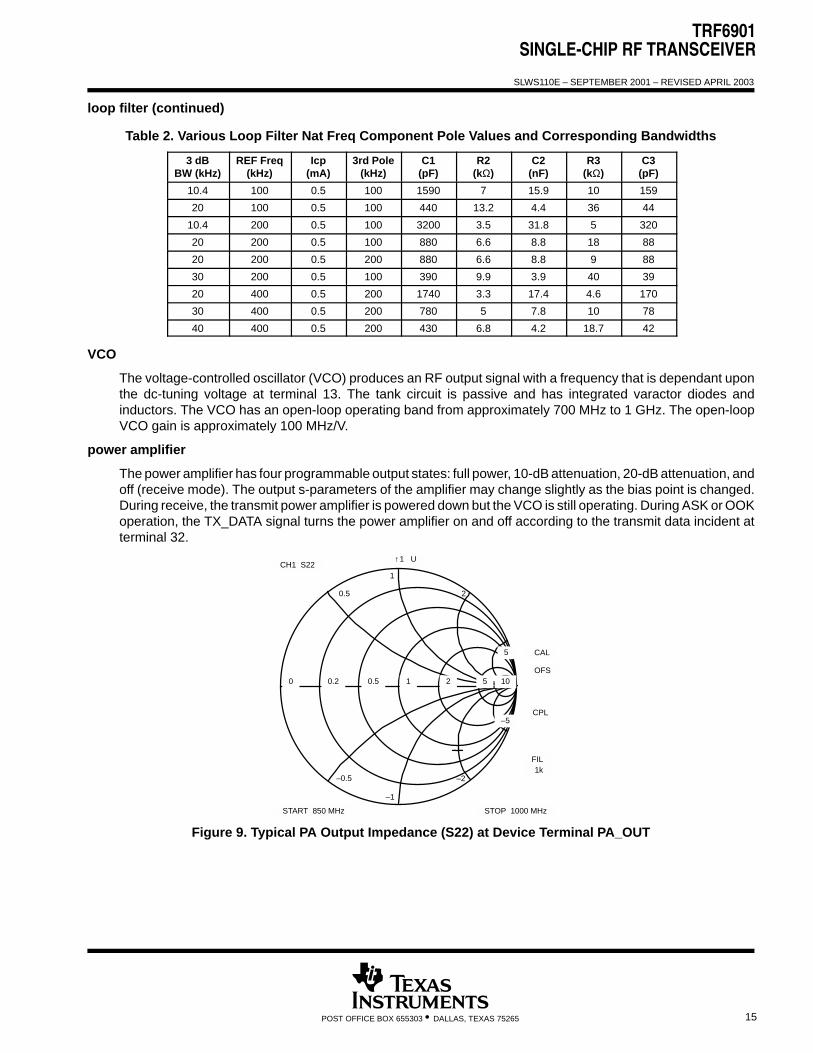
loop filter
The loop filter must be carefully chosen for proper operation of the TRF6901. The loop filter is typically a second-or third-order passive design and in FSK operation should have a bandwidth wide enough to allow the PLL torelock quickly as the external crystal frequency is pulled off-center during modulation. The loop filter should alsobe wider than the data modulation rate. These requirements should be balanced with making the loop narrowenough in consideration of the reference frequency. In OOK the VCO frequency is not changed during datamodulation, so the filter bandwidth may be narrower than the modulation bandwidth. Filters can be calculatedusing standard formulas in reference literature. Some third-order filter examples are shown in Table 2.
F(s) 1 sC2R2s(C1 C2 sC1C2R2)
1C3R3
s 1C3R3
C1
lcp
C2
R2
C3
VtuneR3
External-Loop Filter
15 13
VCO_VCC
VCO_TUNECP_OUT
Figure 8. Third-Order Loop Filter and Transfer Function
TRF6901SINGLE-CHIP RF TRANSCEIVER
SLWS110E – SEPTEMBER 2001 – REVISED APRIL 2003
15POST OFFICE BOX 655303 • DALLAS, TEXAS 75265
loop filter (continued)
Table 2. Various Loop Filter Nat Freq Component Pole Values and Corresponding Bandwidths
3 dBBW (kHz)
REF Freq(kHz)
Icp(mA)
3rd Pole(kHz)
C1(pF)
R2(kΩ)
C2(nF)
R3(kΩ)
C3(pF)
10.4 100 0.5 100 1590 7 15.9 10 159
20 100 0.5 100 440 13.2 4.4 36 44
10.4 200 0.5 100 3200 3.5 31.8 5 320
20 200 0.5 100 880 6.6 8.8 18 88
20 200 0.5 200 880 6.6 8.8 9 88
30 200 0.5 100 390 9.9 3.9 40 39
20 400 0.5 200 1740 3.3 17.4 4.6 170
30 400 0.5 200 780 5 7.8 10 78
40 400 0.5 200 430 6.8 4.2 18.7 42
VCO
The voltage-controlled oscillator (VCO) produces an RF output signal with a frequency that is dependant uponthe dc-tuning voltage at terminal 13. The tank circuit is passive and has integrated varactor diodes andinductors. The VCO has an open-loop operating band from approximately 700 MHz to 1 GHz. The open-loopVCO gain is approximately 100 MHz/V.
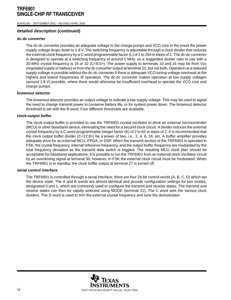
power amplifier
The power amplifier has four programmable output states: full power, 10-dB attenuation, 20-dB attenuation, andoff (receive mode). The output s-parameters of the amplifier may change slightly as the bias point is changed.During receive, the transmit power amplifier is powered down but the VCO is still operating. During ASK or OOKoperation, the TX_DATA signal turns the power amplifier on and off according to the transmit data incident atterminal 32.
0.5
1
↑1 U
2
5
10210.50.20
–0.5
–1
–2
–5
START 850 MHz STOP 1000 MHz
CH1 S22
CAL
OFS
CPL
FIL1k
5
Figure 9. Typical PA Output Impedance (S22) at Device Terminal PA_OUT
TRF6901SINGLE-CHIP RF TRANSCEIVER
SLWS110E – SEPTEMBER 2001 – REVISED APRIL 2003
16 POST OFFICE BOX 655303 • DALLAS, TEXAS 75265
detailed description (continued)
dc-dc converter
The dc-dc converter provides an adequate voltage to the charge pumps and VCO core in the event the powersupply voltage drops down to 1.8 V. The switching frequency is adjustable through a clock divider that reducesthe external clock frequency by a C-word programmable factor (L) of 2 to 254 in steps of 2. The dc-dc converteris designed to operate at a switching frequency of around 1 MHz, so a suggested divider ratio to use with a20-MHz crystal frequency is 16 or 32 (C<6:0>). The power supply to terminals 10 and 16 may be from Vcc(regulated supply or battery) or from the dc converter output at terminal 22, but not both. Operation at a reducedsupply voltage is possible without the dc-dc converter if there is adequate VCO tuning voltage overhead at thehighest and lowest frequencies of operation. The dc-dc converter makes operation at low supply voltages(around 1.8 V) possible, where there would otherwise be insufficient overhead to operate the VCO core andcharge pumps.
brownout detector
The brownout detector provides an output voltage to indicate a low supply voltage. This may be used to signalthe need to change transmit power to conserve battery life, or for system power down. The brownout detectorthreshold is set with the B word. Four different thresholds are available.
clock-output buffer
The clock-output buffer is provided to use the TRF6901 crystal oscillator to drive an external microcontroller(MCU) or other baseband device, eliminating the need for a second clock circuit. A divider reduces the externalcrystal frequency by a C-word programmable integer factor (K) of 2 to 62 in steps of 2. It is recommended thatthe clock output buffer divider (C<12:8>) be a power of two, i.e., 2, 4, 8, 16, etc. A buffer amplifier providesadequate drive for an external MCU, FPGA, or DSP. When the transmit section of the TRF6901 is operated inFSK, the crystal frequency, internal reference frequency, and the output buffer frequency are modulated by thetotal frequency deviation as the transmit data switch is toggled. The resulting MCU clock jitter should beacceptable for baseband applications. It is possible to run the TRF6901 from an external clock oscillator circuitby an overdriving signal at terminal 30; however, in FSK the external clock circuit must be modulated. Whenthe TRF6901 is in standby, the clock buffer output at terminal 27 is turned off.
serial control interface
The TRF6901 is controlled through a serial interface; there are four 24-bit control words (A, B, C, D) which setthe device state. The A and B words are almost identical and provide configuration settings for two modes,designated 0 and 1, which are commonly used to configure the transmit and receive states. The transmit andreceive states can then be rapidly selected using MODE (terminal 21). The C word sets the various clockdividers. The D word is used to trim the external crystal frequency and tune the demodulator.
TRF6901SINGLE-CHIP RF TRANSCEIVER
SLWS110E – SEPTEMBER 2001 – REVISED APRIL 2003
17POST OFFICE BOX 655303 • DALLAS, TEXAS 75265
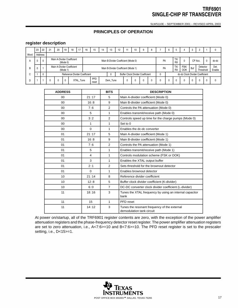
PRINCIPLES OF OPERATION
register description23 22 21 20 19 18 17 16 15 14 13 12 11 10 9 8 7 6 5 4 3 2 1 0
Word Address
A 0 0 Main A-Divider Coefficient (Mode 0)
Main B-Divider Coefficient (Mode 0) PA TX/RX
0 CP Acc. 0 dc-dc
B 0 1 Main A-Divider Coefficient (Mode 1)
Main B-Divider Coefficient (Mode 1) PA TX/RX
FSK/OOK
Buf DetectorThreshold
Det.Enable
C 1 0 Reference Divider Coefficient 0 Buffer Clock Divider Coefficient 0 dc-dc Clock Divider Coefficient
D 1 1 0 0 0 XTAL_Tune PFDreset
Dem_Tune 0 0 0 0 0 0 0 0 0 0 0 0
ADDRESS BITS DESCRIPTION
00 21:17 5 Main A-divider coefficient (Mode 0)
00 16:8 9 Main B-divider coefficient (Mode 0)
00 7 :6 2 Controls the PA attenuation (Mode 0)
00 5 1 Enables transmit/receive path (Mode 0)
00 3 :2 2 Controls speed up time for the charge pumps (Mode 0)
00 1 1 Set to 0
00 0 1 Enables the dc-dc converter
01 21:17 5 Main A-divider coefficient (Mode 1)
01 16:8 9 Main B-divider coefficient (Mode 1)
01 7 :6 2 Controls the PA attenuation (Mode 1)
01 5 1 Enables transmit/receive path (Mode 1)
01 4 1 Controls modulation scheme (FSK or OOK)
01 3 1 Enables the XTAL output buffer
01 2 :1 2 Sets threshold for the brownout detector
01 0 1 Enables brownout detector
10 21:14 8 Reference divider coefficient
10 12:8 5 Buffer clock divider coefficient (K-divider)
10 6 :0 7 DC-DC converter clock divider coefficient (L-divider)
11 18:16 3 Tunes the XTAL frequency by using an internal capacitorbank
11 15 1 PFD reset
11 14:12 3 Tunes the resonant frequency of the externaldemodulation tank circuit
At power on/startup, all of the TRF6901 register contents are zero, with the exception of the power amplifierattenuation registers and the phase-frequency detector reset register. The power amplifier attenuation registersare set to zero attenuation, i.e., A<7:6>=10 and B<7:6>=10. The PFD reset register is set to the prescalersetting, i.e., D<15>=1.
TRF6901SINGLE-CHIP RF TRANSCEIVER
SLWS110E – SEPTEMBER 2001 – REVISED APRIL 2003
18 POST OFFICE BOX 655303 • DALLAS, TEXAS 75265
PRINCIPLES OF OPERATION
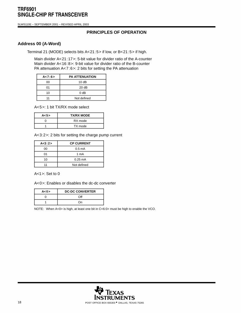
Address 00 (A-Word)
Terminal 21 (MODE) selects bits A<21:5> if low, or B<21:5> if high.
Main divider A<21:17>: 5-bit value for divider ratio of the A-counterMain divider A<16:8>: 9-bit value for divider ratio of the B-counterPA attenuation A<7:6>: 2 bits for setting the PA attenuation
A<7:6> PA ATTENUATION
00 10 dB
01 20 dB
10 0 dB
11 Not defined
A<5>: 1 bit TX/RX mode select
A<5> TX/RX MODE
0 RX mode
1 TX mode
A<3:2>: 2 bits for setting the charge pump current
A<3:2> CP CURRENT
00 0.5 mA
01 1 mA
10 0.25 mA
11 Not defined
A<1>: Set to 0
A<0>: Enables or disables the dc-dc converter
A<0> DC-DC CONVERTER
0 Off
1 On
NOTE: When A<0> is high, at least one bit in C<6:0> must be high to enable the VCO.
TRF6901SINGLE-CHIP RF TRANSCEIVER
SLWS110E – SEPTEMBER 2001 – REVISED APRIL 2003
19POST OFFICE BOX 655303 • DALLAS, TEXAS 75265
PRINCIPLES OF OPERATION
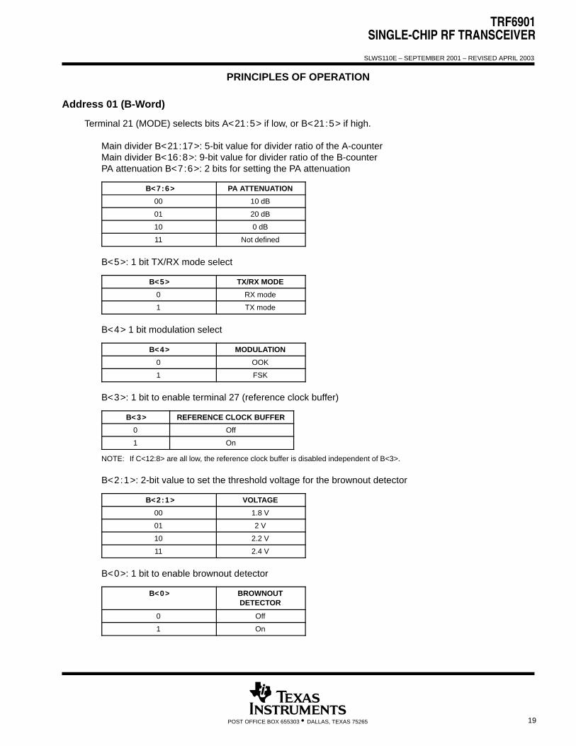
Address 01 (B-Word)
Terminal 21 (MODE) selects bits A<21:5> if low, or B<21:5> if high.
Main divider B<21:17>: 5-bit value for divider ratio of the A-counterMain divider B<16:8>: 9-bit value for divider ratio of the B-counterPA attenuation B<7:6>: 2 bits for setting the PA attenuation
B<7:6> PA ATTENUATION
00 10 dB
01 20 dB
10 0 dB
11 Not defined
B<5>: 1 bit TX/RX mode select
B<5> TX/RX MODE
0 RX mode
1 TX mode
B<4> 1 bit modulation select
B<4> MODULATION
0 OOK
1 FSK
B<3>: 1 bit to enable terminal 27 (reference clock buffer)
B<3> REFERENCE CLOCK BUFFER
0 Off
1 On
NOTE: If C<12:8> are all low, the reference clock buffer is disabled independent of B<3>.
B<2:1>: 2-bit value to set the threshold voltage for the brownout detector
B<2:1> VOLTAGE
00 1.8 V
01 2 V
10 2.2 V
11 2.4 V
B<0>: 1 bit to enable brownout detector
B<0> BROWNOUTDETECTOR
0 Off
1 On
TRF6901SINGLE-CHIP RF TRANSCEIVER
SLWS110E – SEPTEMBER 2001 – REVISED APRIL 2003
20 POST OFFICE BOX 655303 • DALLAS, TEXAS 75265
PRINCIPLES OF OPERATION
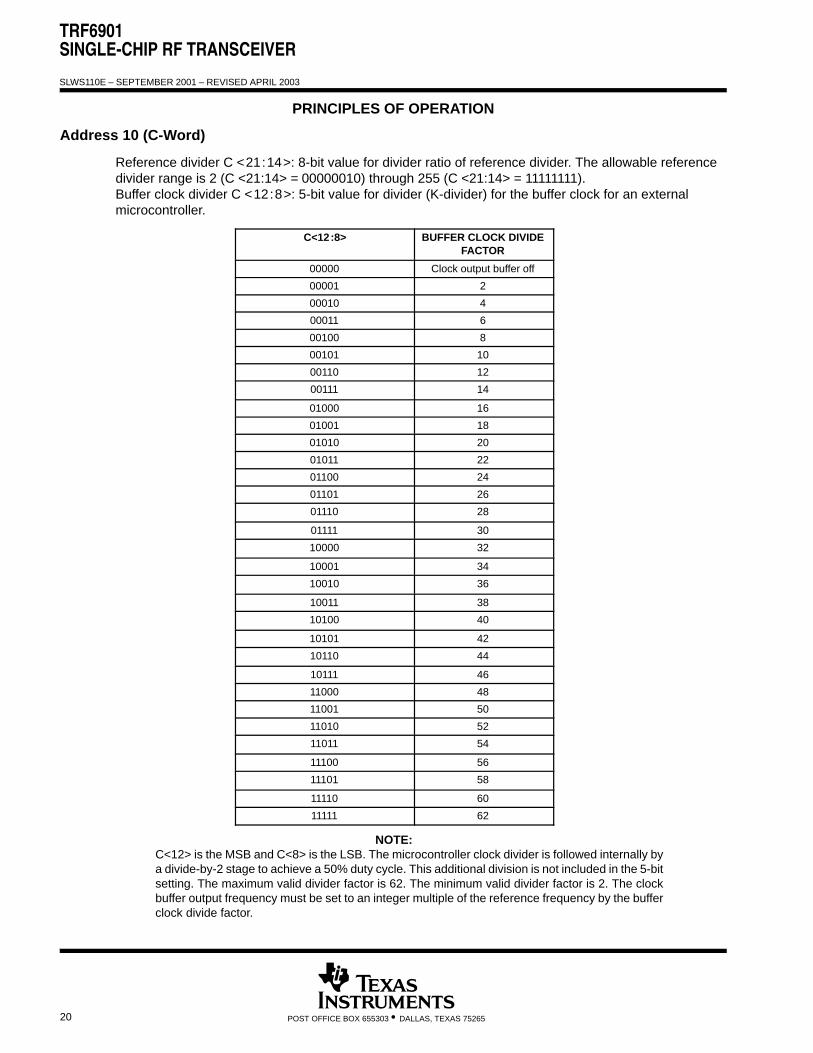
Address 10 (C-Word)
Reference divider C <21:14>: 8-bit value for divider ratio of reference divider. The allowable referencedivider range is 2 (C <21:14> = 00000010) through 255 (C <21:14> = 11111111).Buffer clock divider C <12:8>: 5-bit value for divider (K-divider) for the buffer clock for an externalmicrocontroller.
C<12:8> BUFFER CLOCK DIVIDEFACTOR
00000 Clock output buffer off
00001 2
00010 4
00011 6
00100 8
00101 10
00110 12
00111 14
01000 16
01001 18
01010 20
01011 22
01100 24
01101 26
01110 28
01111 30
10000 32
10001 34
10010 36
10011 38
10100 40
10101 42
10110 44
10111 46
11000 48
11001 50
11010 52
11011 54
11100 56
11101 58
11110 60
11111 62
NOTE:C<12> is the MSB and C<8> is the LSB. The microcontroller clock divider is followed internally bya divide-by-2 stage to achieve a 50% duty cycle. This additional division is not included in the 5-bitsetting. The maximum valid divider factor is 62. The minimum valid divider factor is 2. The clockbuffer output frequency must be set to an integer multiple of the reference frequency by the bufferclock divide factor.
TRF6901SINGLE-CHIP RF TRANSCEIVER
SLWS110E – SEPTEMBER 2001 – REVISED APRIL 2003
21POST OFFICE BOX 655303 • DALLAS, TEXAS 75265
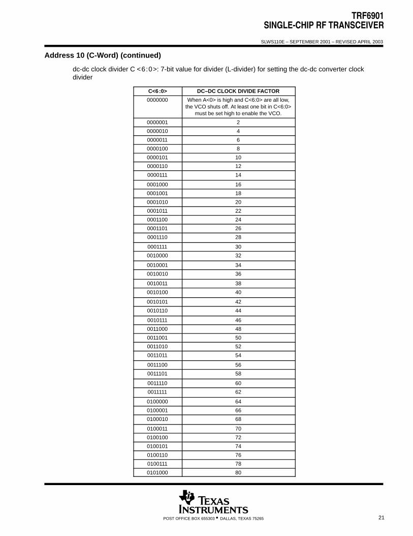
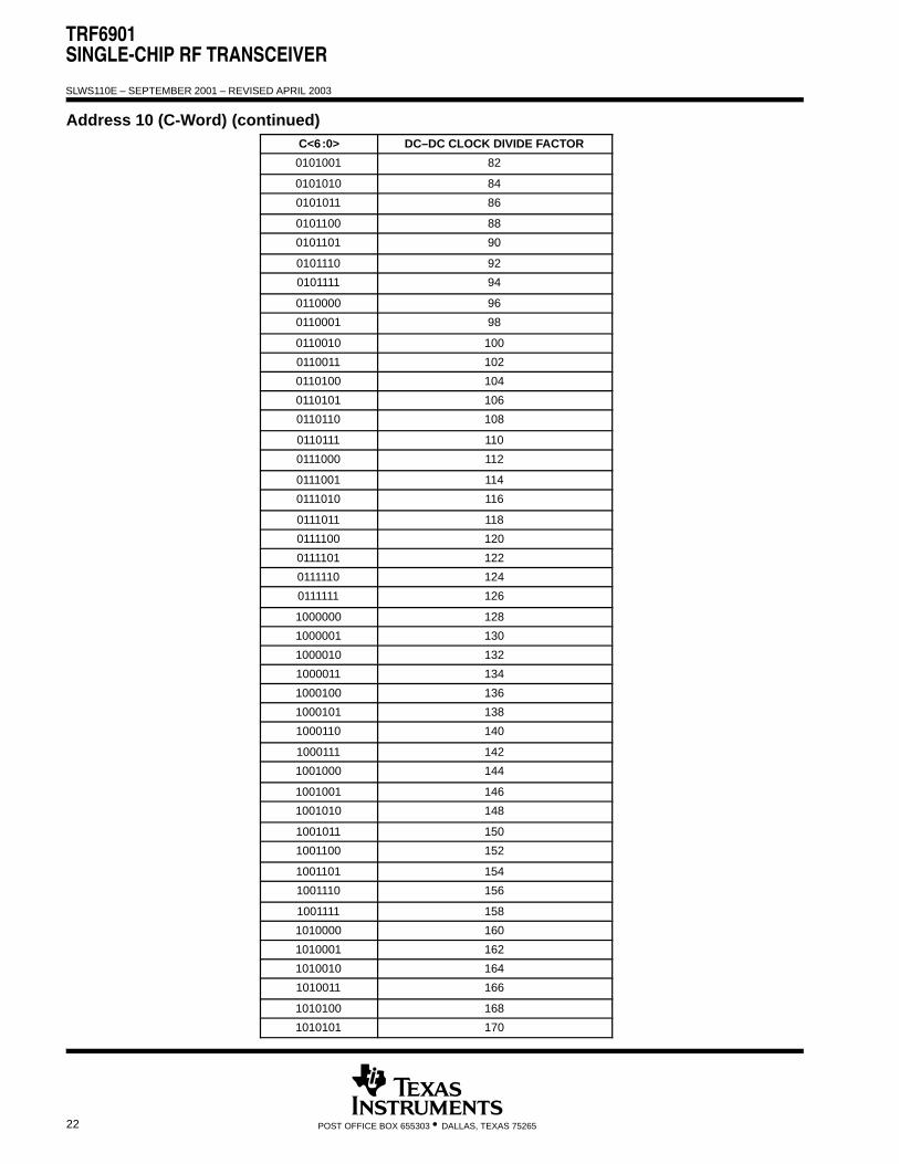
Address 10 (C-Word) (continued)
dc-dc clock divider C <6:0>: 7-bit value for divider (L-divider) for setting the dc-dc converter clockdivider
C<6:0> DC–DC CLOCK DIVIDE FACTOR
0000000 When A<0> is high and C<6:0> are all low,the VCO shuts off. At least one bit in C<6:0>
must be set high to enable the VCO.
0000001 2
0000010 4
0000011 6
0000100 8
0000101 10
0000110 12
0000111 14
0001000 16
0001001 18
0001010 20
0001011 22
0001100 24
0001101 26
0001110 28
0001111 30
0010000 32
0010001 34
0010010 36
0010011 38
0010100 40
0010101 42
0010110 44
0010111 46
0011000 48
0011001 50
0011010 52
0011011 54
0011100 56
0011101 58
0011110 60
0011111 62
0100000 64
0100001 66
0100010 68
0100011 70
0100100 72
0100101 74
0100110 76
0100111 78
0101000 80
TRF6901SINGLE-CHIP RF TRANSCEIVER
SLWS110E – SEPTEMBER 2001 – REVISED APRIL 2003
22 POST OFFICE BOX 655303 • DALLAS, TEXAS 75265
Address 10 (C-Word) (continued)C<6:0> DC–DC CLOCK DIVIDE FACTOR
0101001 82
0101010 84
0101011 86
0101100 88
0101101 90
0101110 92
0101111 94
0110000 96
0110001 98
0110010 100
0110011 102
0110100 104
0110101 106
0110110 108
0110111 110
0111000 112
0111001 114
0111010 116
0111011 118
0111100 120
0111101 122
0111110 124
0111111 126
1000000 128
1000001 130
1000010 132
1000011 134
1000100 136
1000101 138
1000110 140
1000111 142
1001000 144
1001001 146
1001010 148
1001011 150
1001100 152
1001101 154
1001110 156
1001111 158
1010000 160
1010001 162
1010010 164
1010011 166
1010100 168
1010101 170
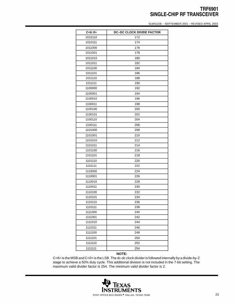
TRF6901SINGLE-CHIP RF TRANSCEIVER
SLWS110E – SEPTEMBER 2001 – REVISED APRIL 2003
23POST OFFICE BOX 655303 • DALLAS, TEXAS 75265
C<6:0> DC–DC CLOCK DIVIDE FACTOR
1010110 172
1010111 174
1011000 176
1011001 178
1011010 180
1011011 182
1011100 184
1011101 186
1011110 188
1011111 190
1100000 192
1100001 194
1100010 196
1100011 198
1100100 200
1100101 202
1100110 204
1100111 206
1101000 208
1101001 210
1101010 212
1101011 214
1101100 216
1101101 218
1101110 220
1101111 222
1110000 224
1110001 226
1110010 228
1110011 230
1110100 232
1110101 234
1110110 236
1110111 238
1111000 240
1111001 242
1111010 244
1111011 246
1111100 248
1111101 250
1111110 252
1111111 254
NOTE:C<6> is the MSB and C<0> is the LSB. The dc-dc clock divider is followed internally by a divide-by-2stage to achieve a 50% duty cycle. This additional division is not included in the 7-bit setting. Themaximum valid divider factor is 254. The minimum valid divider factor is 2.
TRF6901SINGLE-CHIP RF TRANSCEIVER
SLWS110E – SEPTEMBER 2001 – REVISED APRIL 2003
24 POST OFFICE BOX 655303 • DALLAS, TEXAS 75265
PRINCIPLES OF OPERATION
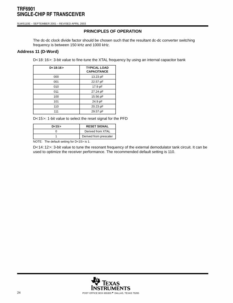
The dc-dc clock divide factor should be chosen such that the resultant dc-dc converter switchingfrequency is between 150 kHz and 1000 kHz.
Address 11 (D-Word)
D<18:16>: 3-bit value to fine-tune the XTAL frequency by using an internal capacitor bank
D<18:16> TYPICAL LOADCAPACITANCE
000 13.23 pF
001 22.57 pF
010 17.9 pF
011 27.24 pF
100 15.56 pF
101 24.9 pF
110 20.23 pF
111 29.57 pF
D<15>: 1-bit value to select the reset signal for the PFD
D<15> RESET SIGNAL
0 Derived from XTAL
1 Derived from prescaler
NOTE: The default setting for D<15> is 1.
D<14:12>: 3-bit value to tune the resonant frequency of the external demodulator tank circuit. It can beused to optimize the receiver performance. The recommended default setting is 110.
TRF6901SINGLE-CHIP RF TRANSCEIVER
SLWS110E – SEPTEMBER 2001 – REVISED APRIL 2003
25POST OFFICE BOX 655303 • DALLAS, TEXAS 75265
PRINCIPLES OF OPERATION
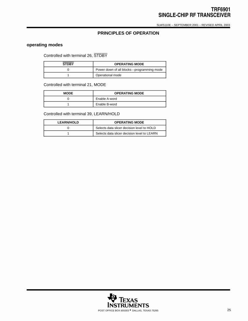
operating modes
Controlled with terminal 26, STDBY
STDBY OPERATING MODE
0 Power down of all blocks—programming mode
1 Operational mode
Controlled with terminal 21, MODE
MODE OPERATING MODE
0 Enable A-word
1 Enable B-word
Controlled with terminal 39, LEARN/HOLD
LEARN/HOLD OPERATING MODE
0 Selects data slicer decision level to HOLD
1 Selects data slicer decision level to LEARN
TRF6901SINGLE-CHIP RF TRANSCEIVER
SLWS110E – SEPTEMBER 2001 – REVISED APRIL 2003
26 POST OFFICE BOX 655303 • DALLAS, TEXAS 75265
APPLICATION INFORMATION
ReferenceGenerator
DC-DCConverter
PA
LNA
RSSI
LPF
_IN
LEA
RN
/
RS
SI_
IF_I
N2
IF_I
N1
DE
T_O
UT
MIX
_OU
T
HO
LDOU
T
373839404142434445464748
242322212019181716151413
36
35
34
33
32
31
30
29
28
27
26
25
1
2
3
4
5
6
7
8
9
10
11
12
Dataslicer
LPF_OUT
CER_DIS
SLC_CAP
RX_DATA
TX_DATA
XTAL_SW
XTAL
CLKTST_OUT
DC_DC_IN
C1
C2
CP
_VC
C
CP
_OU
T
VC
O_T
UN
E
PA_OUT
PA_VCC
VCO_VCC
VCO_TANK2
VCO_TANK1
U1TRF6901
PLL
VCO
C122.7 pF
C162.7 pF
L210 nH
C13
22 pF
C15
RX_IN+
LNA_VCC
VCO_VCC
L68.2 nH
C21
1.8 pF
PA_VCC
TX_OUT
J2
J4
J1
C23150 pF
C27100 pF
C260.1 µ F
VCO_VCC2
DCDC_OUT
C36
100 pF R1418 kΩ
C44
1000 pF
R19
6.8 kΩ
C49
10000 pF
DV
DD
CLO
CK
ST
RO
BE
DA
TA
MO
DE
C35
0.22 µ F
DCDC_OUT
VCO_VCC2
C450.1 µ F
C4610000 pF
21
3
DCDC_OUT
XTAL1
C22 68 pF
C24
15 pF
DCDC_VCC
STDBY
MCU_CLK
XTAL_VCC
TX_DATA
RX_DATA
C20 2200 pF DIS110.7
C14 82 pF
R5220 kΩ
LRN
/HO
LD
DE
M_V
CC
RS
SI
DE
T_O
UT
L3
4.7 µ H
MIX
_VC
C
C515 pF
C4
82 pF C682 pF
BPF1SFECV10.7 MA 2S–A
BW = 330 kHz
1
2
3
C7120 pF
C968 pF
12
3
L14.7 µ H
C310.1 Fµ
JP1
JP3
CDACV10M7GA001
SMI97SMX(C)– 20 MHZ
CDSCA10M7GA119,or
CDSCB10M7GA119,
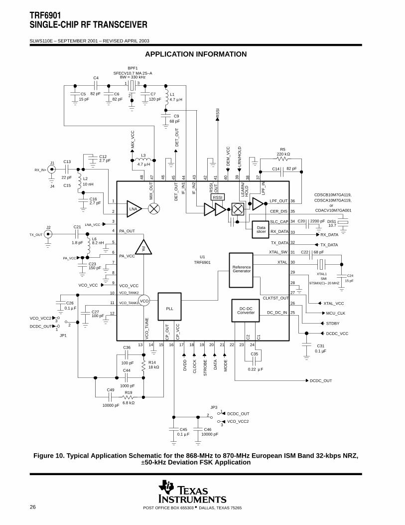
Figure 10. Typical Application Schematic for the 868-MHz to 870-MHz European ISM Band 32-kbps NRZ,±50-kHz Deviation FSK Application
TRF6901SINGLE-CHIP RF TRANSCEIVER
SLWS110E – SEPTEMBER 2001 – REVISED APRIL 2003
27POST OFFICE BOX 655303 • DALLAS, TEXAS 75265
APPLICATION INFORMATION
ReferenceGenerator
DC-DCConverter
PA
LNA
RSSI
LPF
_IN
LEA
RN
/
RS
SI_
IF_I
N2
IF_I
N1
DE
T_O
UT
MIX
_OU
T
HO
LDOU
T
373839404142434445464748
242322212019181716151413
36
35
34
33
32
31
30
29
28
27
26
25
1
2
3
4
5
6
7
8
9
10
11
12
Dataslicer
LPF_OUT
CER_DIS
SLC_CAP
RX_DATA
TX_DATA
XTAL_SW
XTAL
CLKTST_OUT
DC_DC_IN
C1
C2
CP
_VC
C
CP
_OU
T
VC
O_T
UN
E
PA_OUT
PA_VCC
VCO_VCC
VCO_TANK2
VCO_TANK1
U1TRF6901
PLL
VCO
C122.7 pF
C162.7 pF
L210 nH
C13
22 pF
C15
RX_IN+
LNA_VCC
VCO_VCC
L68.2 nH
C21
1.8 pF
PA_VCC
TX_OUT
J2
J4
J1
C23150 pF
C27100 pF
C260.1 µ F
VCO_VCC2
DCDC_OUT
C36
100 pF R1418 kΩ
C44
1000 pF
R19
6.8 kΩ
C49
10000 pF
DV
DD
CLO
CK
ST
RO
BE
DA
TA
MO
DE
C35
0.22 µ F
DCDC_OUT
VCO_VCC2
C450.1 µ F
C4610000 pF
21
3
DCDC_OUT
XTAL1
C22 68 pF
C24
15 pF
DCDC_VCC
STDBY
MCU_CLK
XTAL_VCC
TX_DATA
RX_DATA
C20 2200 pF DIS110.7
C14 82 pF
R5220 kΩ
LRN
/HO
LD
DE
M_V
CC
RS
SI
DE
T_O
UT
L3
4.7 µ H
MIX
_VC
C
C515 pF
C4
82 pF C682 pF
BPF1SFECV10.7 MA 2S–A
BW = 330 kHz
1
2
3
C7120 pF
C968 pF
12
3
L14.7 µ H
C310.1 Fµ
JP1
JP3
R13
100Ω
L747µ H
C370.47 Fµ
C38 1 Fµ
C390.47 Fµ
CDACV10M7GA001
SMI97SMX(C)– 20 MHZ
CDSCA10M7GA119,or
CDSCB10M7GA119,
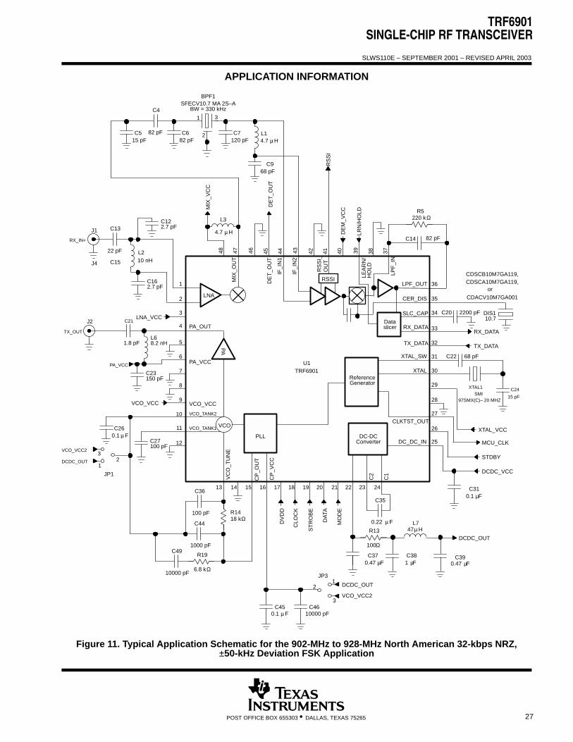
Figure 11. Typical Application Schematic for the 902-MHz to 928-MHz North American 32-kbps NRZ,±50-kHz Deviation FSK Application
MECHANICAL DATA
MTQF003A – OCTOBER 1994 – REVISED DECEMBER 1996
1POST OFFICE BOX 655303 • DALLAS, TEXAS 75265
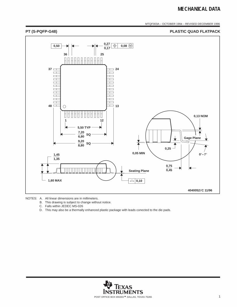
PT (S-PQFP-G48) PLASTIC QUAD FLATPACK
4040052/C 11/96
0,13 NOM
0,170,27
25
24
SQ
12
13
36
37
6,807,20
1
48
5,50 TYP
0,25
0,450,75
0,05 MIN
SQ9,208,80
1,351,45
1,60 MAX
Gage Plane
Seating Plane
0,10
0°–7°
0,50 M0,08
NOTES: A. All linear dimensions are in millimeters.B. This drawing is subject to change without notice.C. Falls within JEDEC MS-026D. This may also be a thermally enhanced plastic package with leads conected to the die pads.
IMPORTANT NOTICE
Texas Instruments Incorporated and its subsidiaries (TI) reserve the right to make corrections, modifications,enhancements, improvements, and other changes to its products and services at any time and to discontinueany product or service without notice. Customers should obtain the latest relevant information before placingorders and should verify that such information is current and complete. All products are sold subject to TI’s termsand conditions of sale supplied at the time of order acknowledgment.
TI warrants performance of its hardware products to the specifications applicable at the time of sale inaccordance with TI’s standard warranty. Testing and other quality control techniques are used to the extent TIdeems necessary to support this warranty. Except where mandated by government requirements, testing of allparameters of each product is not necessarily performed.
TI assumes no liability for applications assistance or customer product design. Customers are responsible fortheir products and applications using TI components. To minimize the risks associated with customer productsand applications, customers should provide adequate design and operating safeguards.
TI does not warrant or represent that any license, either express or implied, is granted under any TI patent right,copyright, mask work right, or other TI intellectual property right relating to any combination, machine, or processin which TI products or services are used. Information published by TI regarding third–party products or servicesdoes not constitute a license from TI to use such products or services or a warranty or endorsement thereof.Use of such information may require a license from a third party under the patents or other intellectual propertyof the third party, or a license from TI under the patents or other intellectual property of TI.
Reproduction of information in TI data books or data sheets is permissible only if reproduction is withoutalteration and is accompanied by all associated warranties, conditions, limitations, and notices. Reproductionof this information with alteration is an unfair and deceptive business practice. TI is not responsible or liable forsuch altered documentation.
Resale of TI products or services with statements different from or beyond the parameters stated by TI for thatproduct or service voids all express and any implied warranties for the associated TI product or service andis an unfair and deceptive business practice. TI is not responsible or liable for any such statements.
Mailing Address:
Texas InstrumentsPost Office Box 655303Dallas, Texas 75265
Copyright 2003, Texas Instruments Incorporated