Embed Size (px)
Citation preview
Single Cycle CPU
Jason Mars
Tuesday, February 5, 13
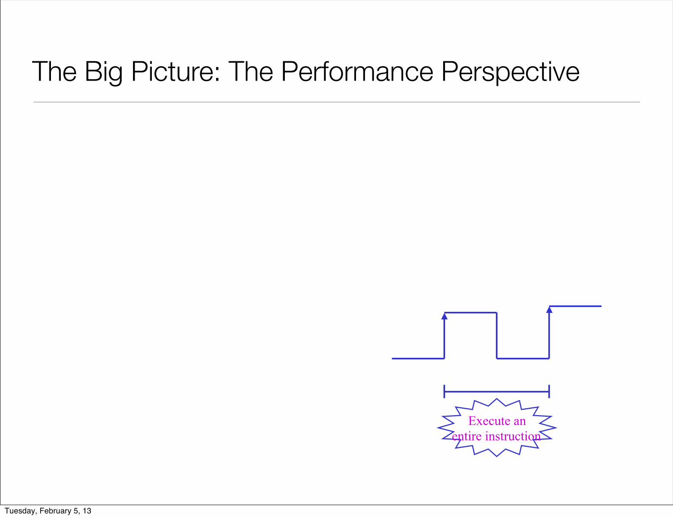
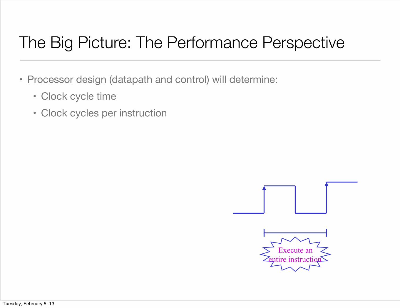
The Big Picture: The Performance Perspective
Execute an entire instruction
Tuesday, February 5, 13
The Big Picture: The Performance Perspective
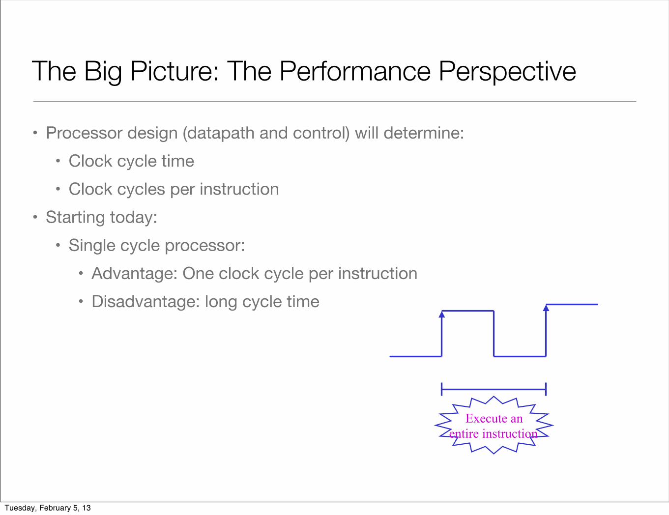
• Processor design (datapath and control) will determine:• Clock cycle time• Clock cycles per instruction
Execute an entire instruction
Tuesday, February 5, 13
The Big Picture: The Performance Perspective
• Processor design (datapath and control) will determine:• Clock cycle time• Clock cycles per instruction
• Starting today:• Single cycle processor:
• Advantage: One clock cycle per instruction• Disadvantage: long cycle time
Execute an entire instruction
Tuesday, February 5, 13
The Big Picture: The Performance Perspective
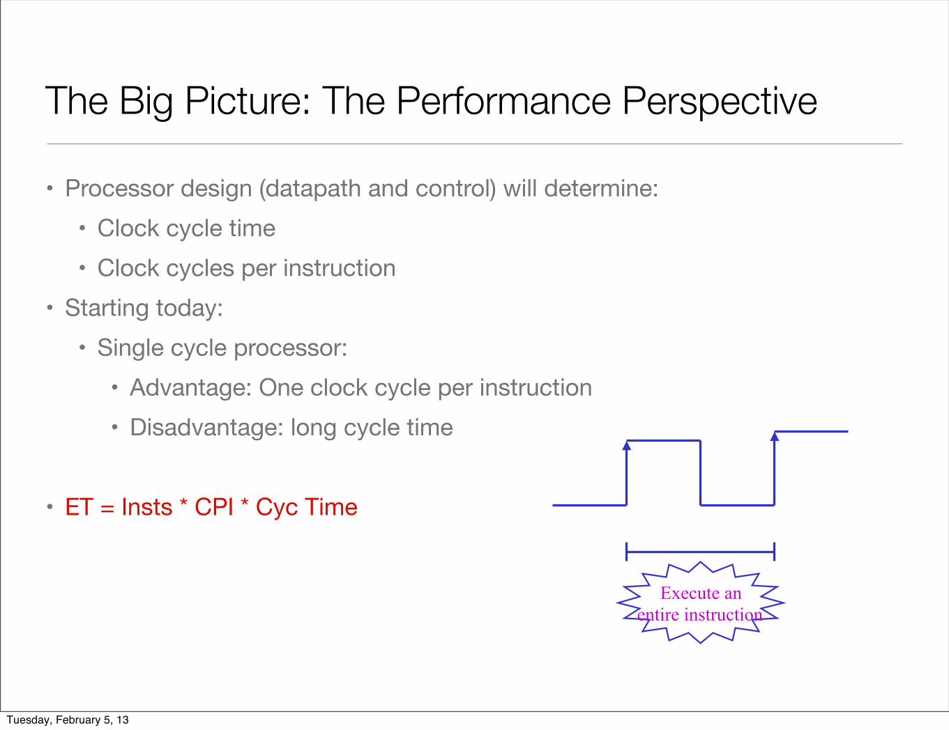
• Processor design (datapath and control) will determine:• Clock cycle time• Clock cycles per instruction
• Starting today:• Single cycle processor:
• Advantage: One clock cycle per instruction• Disadvantage: long cycle time
• ET = Insts * CPI * Cyc Time
Execute an entire instruction
Tuesday, February 5, 13
Processor Datapath and Control
Tuesday, February 5, 13
Processor Datapath and Control
• We're ready to look at an implementation of the MIPS simplified to contain only:• memory-reference instructions: lw, sw • arithmetic-logical instructions: add, sub, and, or, slt• control flow instructions: beq
Tuesday, February 5, 13
Processor Datapath and Control
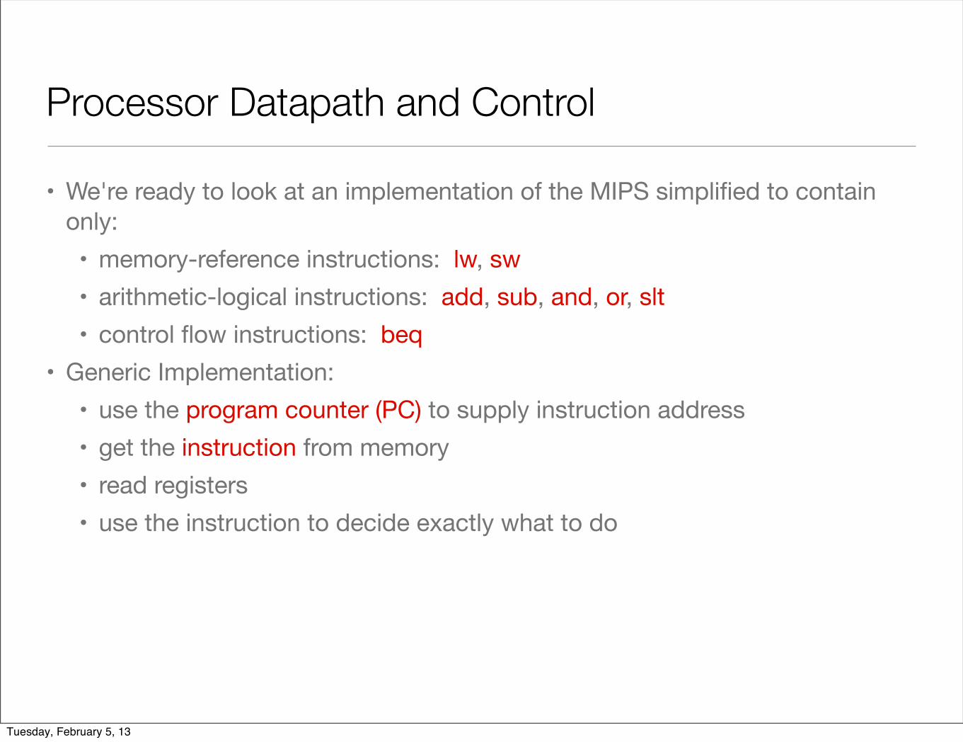
• We're ready to look at an implementation of the MIPS simplified to contain only:• memory-reference instructions: lw, sw • arithmetic-logical instructions: add, sub, and, or, slt• control flow instructions: beq
• Generic Implementation:• use the program counter (PC) to supply instruction address• get the instruction from memory• read registers• use the instruction to decide exactly what to do
Tuesday, February 5, 13
Processor Datapath and Control
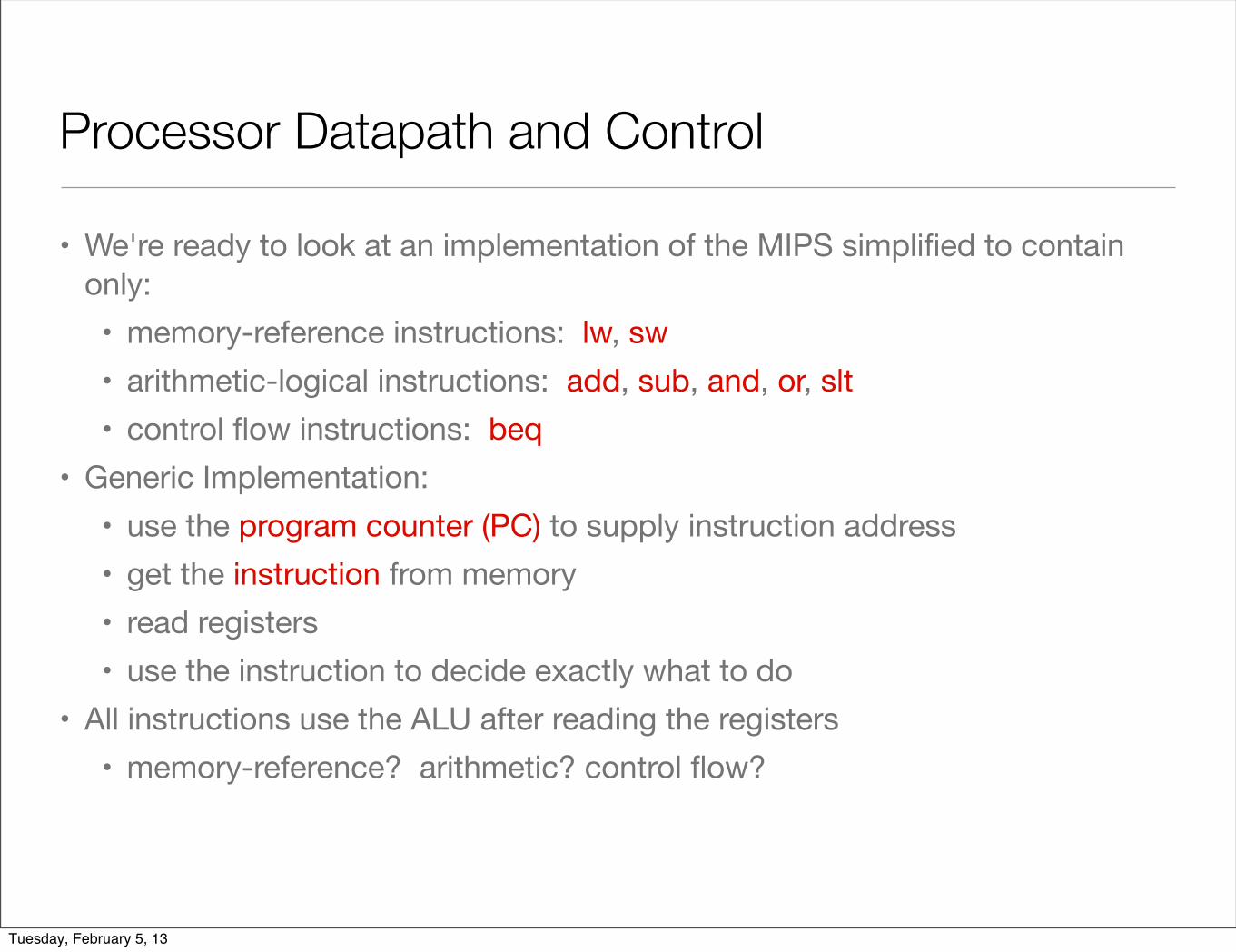
• We're ready to look at an implementation of the MIPS simplified to contain only:• memory-reference instructions: lw, sw • arithmetic-logical instructions: add, sub, and, or, slt• control flow instructions: beq
• Generic Implementation:• use the program counter (PC) to supply instruction address• get the instruction from memory• read registers• use the instruction to decide exactly what to do
• All instructions use the ALU after reading the registers• memory-reference? arithmetic? control flow?
Tuesday, February 5, 13
Review: MIPS Instruction Formats
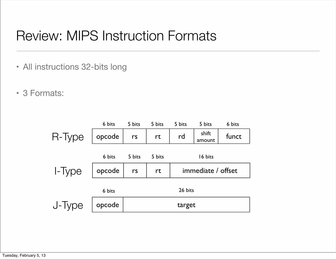
• All instructions 32-bits long
• 3 Formats:
opcode target
opcode rs rt rd shift amount funct
opcode rs rt immediate / offset
6 bits 5 bits 5 bits 5 bits 5 bits 6 bits
6 bits 5 bits 5 bits 16 bits
6 bits 26 bits
I-Type
J-Type
R-Type
Tuesday, February 5, 13
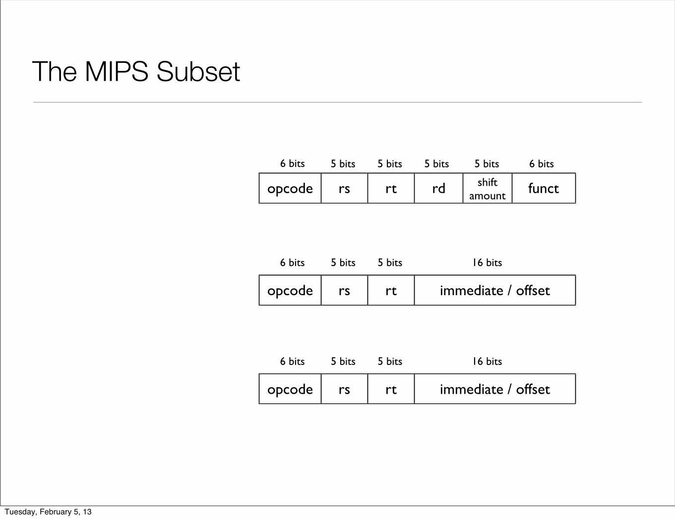
The MIPS Subset
opcode rs rt immediate / offset
6 bits 5 bits 5 bits 16 bits
opcode rs rt rd shift amount funct
6 bits 5 bits 5 bits 5 bits 5 bits 6 bits
opcode rs rt immediate / offset
6 bits 5 bits 5 bits 16 bits
Tuesday, February 5, 13
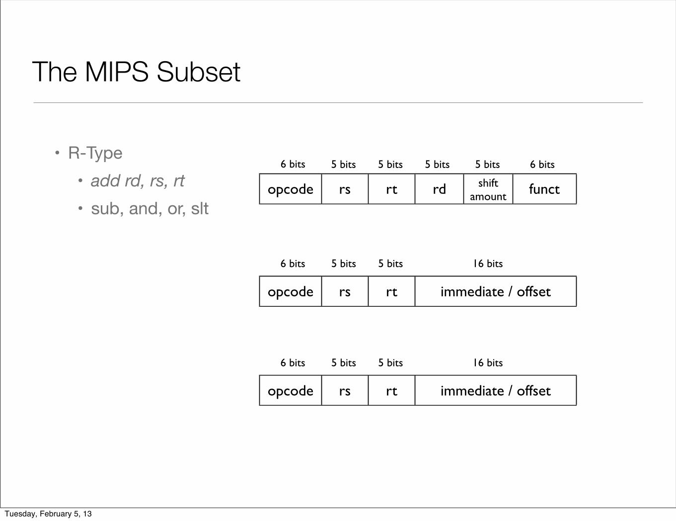
The MIPS Subset
opcode rs rt immediate / offset
6 bits 5 bits 5 bits 16 bits
opcode rs rt rd shift amount funct
6 bits 5 bits 5 bits 5 bits 5 bits 6 bits• R-Type
• add rd, rs, rt• sub, and, or, slt
opcode rs rt immediate / offset
6 bits 5 bits 5 bits 16 bits
Tuesday, February 5, 13

The MIPS Subset
opcode rs rt immediate / offset
6 bits 5 bits 5 bits 16 bits
opcode rs rt rd shift amount funct
6 bits 5 bits 5 bits 5 bits 5 bits 6 bits• R-Type
• add rd, rs, rt• sub, and, or, slt
• LOAD and STORE• lw rt, rs, imm16• sw rt, rs, imm16
opcode rs rt immediate / offset
6 bits 5 bits 5 bits 16 bits
Tuesday, February 5, 13
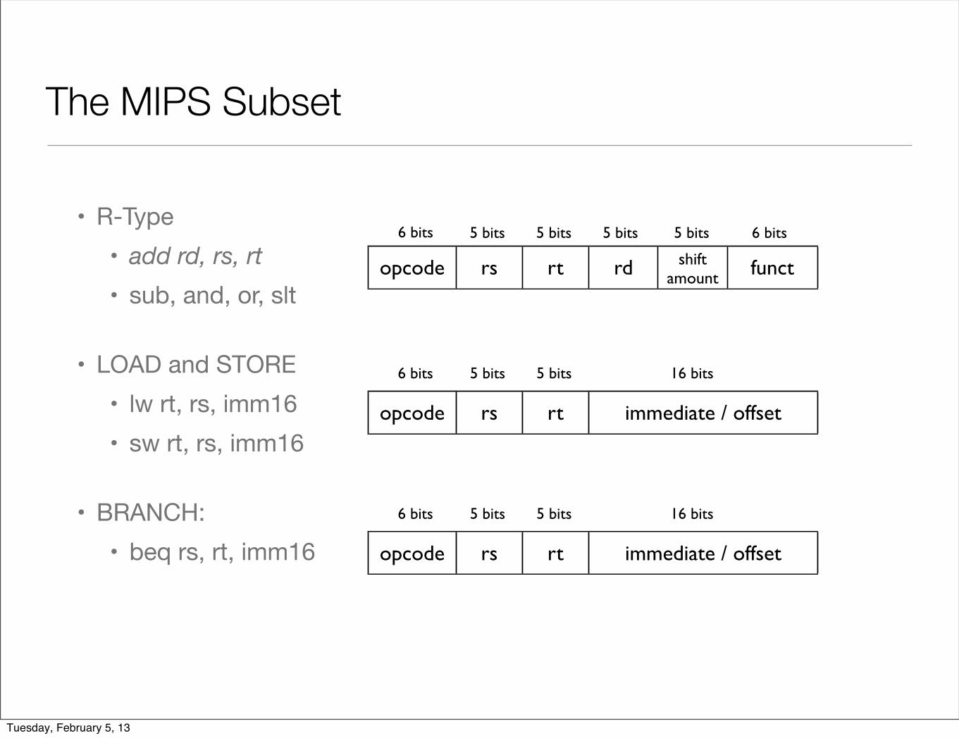
The MIPS Subset
opcode rs rt immediate / offset
6 bits 5 bits 5 bits 16 bits
opcode rs rt rd shift amount funct
6 bits 5 bits 5 bits 5 bits 5 bits 6 bits• R-Type
• add rd, rs, rt• sub, and, or, slt
• LOAD and STORE• lw rt, rs, imm16• sw rt, rs, imm16
• BRANCH:• beq rs, rt, imm16 opcode rs rt immediate / offset
6 bits 5 bits 5 bits 16 bits
Tuesday, February 5, 13
Basic Steps of Execution
Tuesday, February 5, 13

Basic Steps of Execution
• Instruction Fetch• Where is the instruction?
Tuesday, February 5, 13
Basic Steps of Execution
• Instruction Fetch• Where is the instruction?
• Decode• What’s the incoming instruction?• Where are the operands in an instruction?
Tuesday, February 5, 13
Basic Steps of Execution
• Instruction Fetch• Where is the instruction?
• Decode• What’s the incoming instruction?• Where are the operands in an instruction?
• Execution: ALU• What is the function that ALU should perform?
Tuesday, February 5, 13

Basic Steps of Execution
• Instruction Fetch• Where is the instruction?
• Decode• What’s the incoming instruction?• Where are the operands in an instruction?
• Execution: ALU• What is the function that ALU should perform?
• Memory access• Where is my data?
Tuesday, February 5, 13
Basic Steps of Execution
• Instruction Fetch• Where is the instruction?
• Decode• What’s the incoming instruction?• Where are the operands in an instruction?
• Execution: ALU• What is the function that ALU should perform?
• Memory access• Where is my data?
• Write back results to registers• Where to write?
• Determine the next PC
Tuesday, February 5, 13
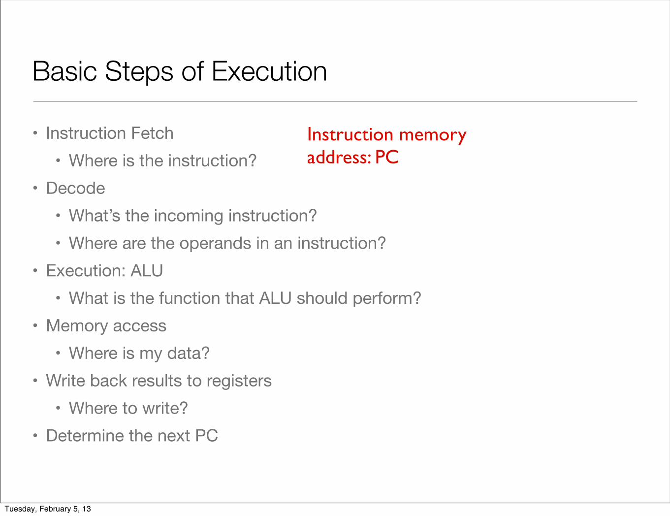
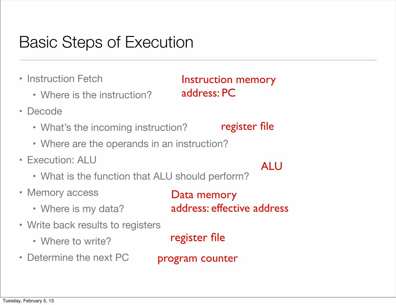
Basic Steps of Execution
• Instruction Fetch• Where is the instruction?
• Decode• What’s the incoming instruction?• Where are the operands in an instruction?
• Execution: ALU• What is the function that ALU should perform?
• Memory access• Where is my data?
• Write back results to registers• Where to write?
• Determine the next PC
Instruction memoryaddress: PC
Tuesday, February 5, 13

Basic Steps of Execution
• Instruction Fetch• Where is the instruction?
• Decode• What’s the incoming instruction?• Where are the operands in an instruction?
• Execution: ALU• What is the function that ALU should perform?
• Memory access• Where is my data?
• Write back results to registers• Where to write?
• Determine the next PC
Instruction memoryaddress: PC
register file
Tuesday, February 5, 13
Basic Steps of Execution
• Instruction Fetch• Where is the instruction?
• Decode• What’s the incoming instruction?• Where are the operands in an instruction?
• Execution: ALU• What is the function that ALU should perform?
• Memory access• Where is my data?
• Write back results to registers• Where to write?
• Determine the next PC
Instruction memoryaddress: PC
register file
ALU
Tuesday, February 5, 13
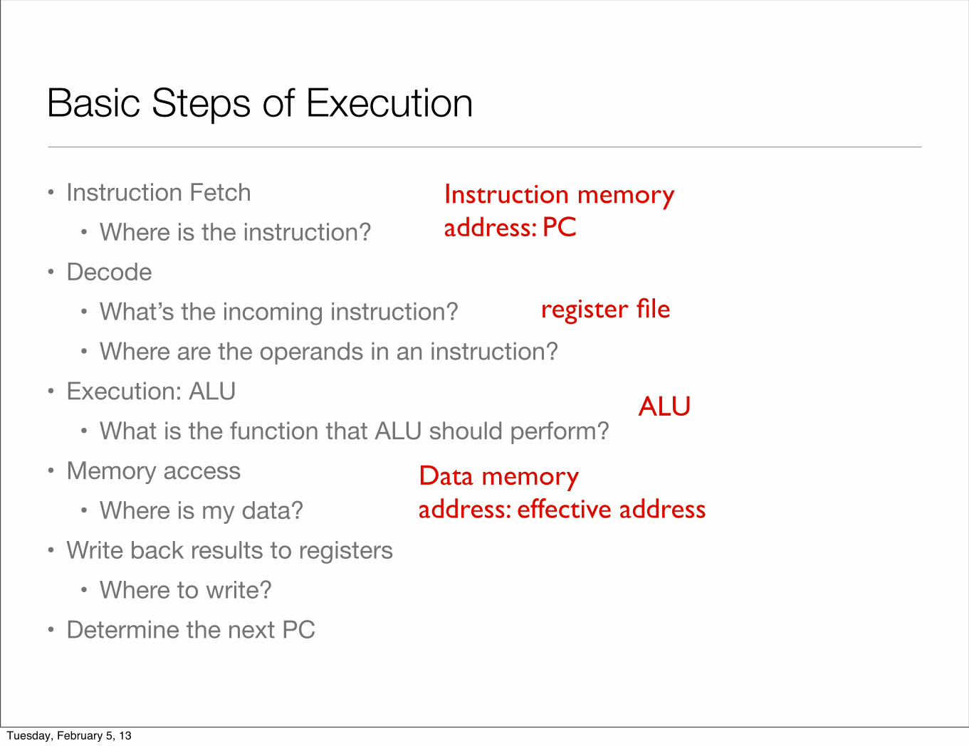
Basic Steps of Execution
• Instruction Fetch• Where is the instruction?
• Decode• What’s the incoming instruction?• Where are the operands in an instruction?
• Execution: ALU• What is the function that ALU should perform?
• Memory access• Where is my data?
• Write back results to registers• Where to write?
• Determine the next PC
Instruction memoryaddress: PC
register file
ALU
Data memoryaddress: effective address
Tuesday, February 5, 13
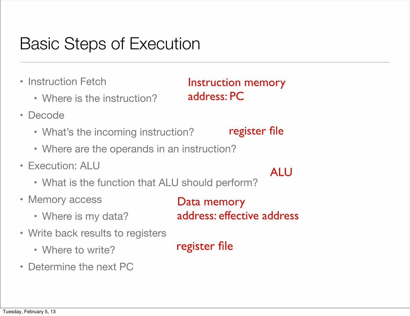
Basic Steps of Execution
• Instruction Fetch• Where is the instruction?
• Decode• What’s the incoming instruction?• Where are the operands in an instruction?
• Execution: ALU• What is the function that ALU should perform?
• Memory access• Where is my data?
• Write back results to registers• Where to write?
• Determine the next PC
Instruction memoryaddress: PC
register file
ALU
Data memoryaddress: effective address
register file
Tuesday, February 5, 13
Basic Steps of Execution
• Instruction Fetch• Where is the instruction?
• Decode• What’s the incoming instruction?• Where are the operands in an instruction?
• Execution: ALU• What is the function that ALU should perform?
• Memory access• Where is my data?
• Write back results to registers• Where to write?
• Determine the next PC
Instruction memoryaddress: PC
register file
ALU
Data memoryaddress: effective address
register file
program counter
Tuesday, February 5, 13
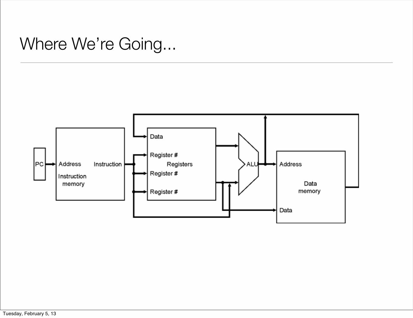
Where We’re Going...
Tuesday, February 5, 13
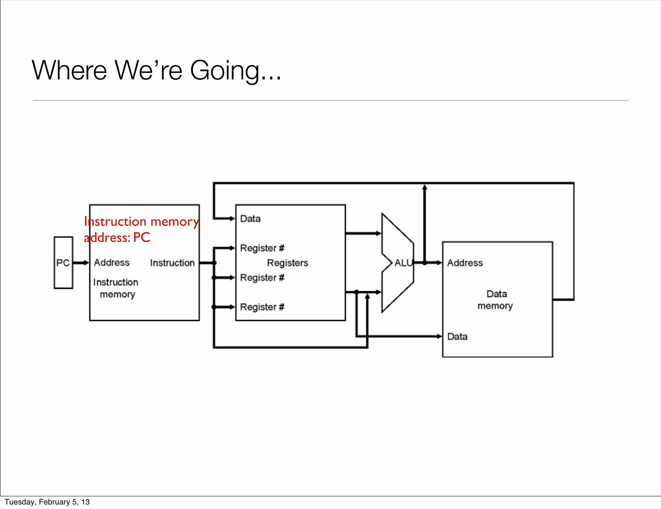
Where We’re Going...
Instruction memoryaddress: PC
Tuesday, February 5, 13
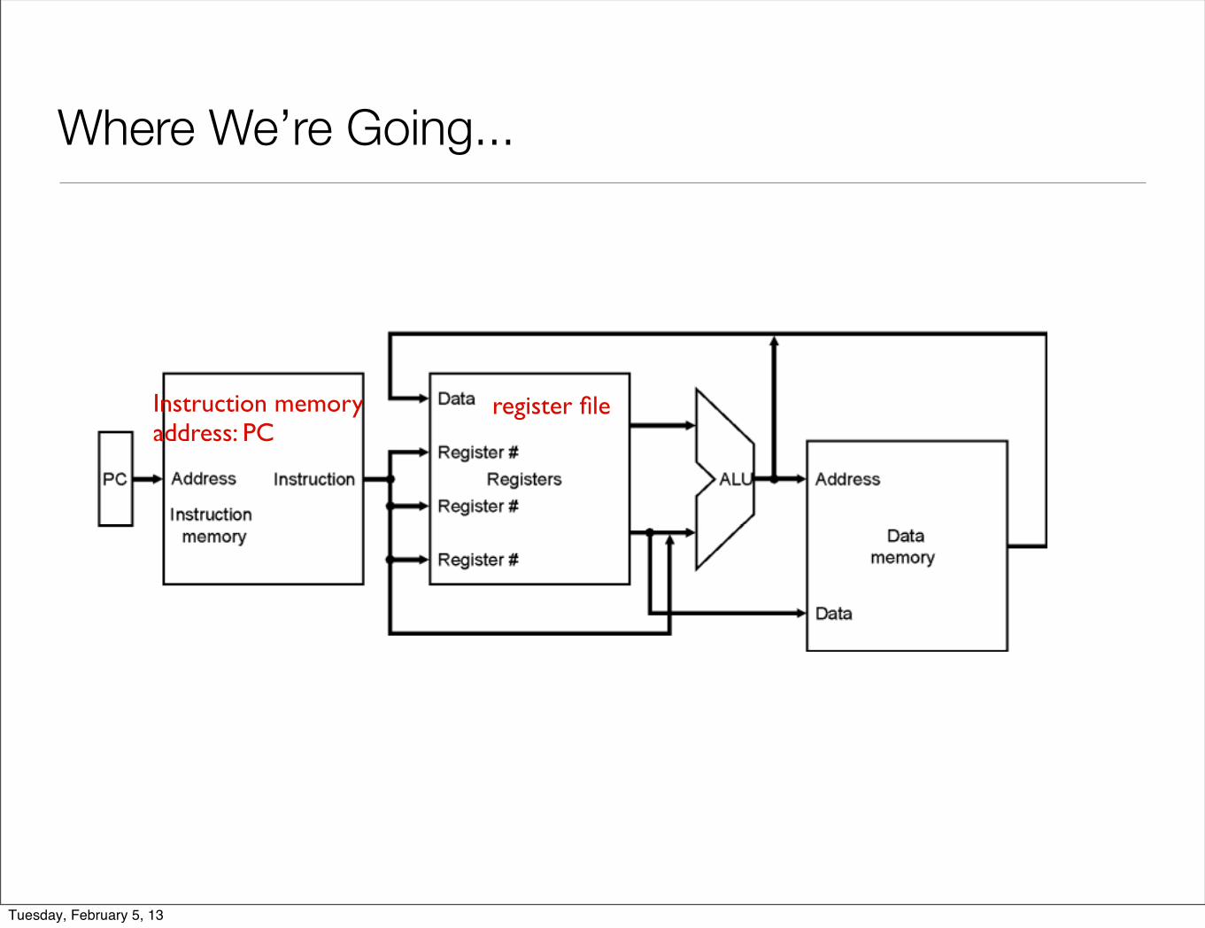
Where We’re Going...
Instruction memoryaddress: PC
register file
Tuesday, February 5, 13
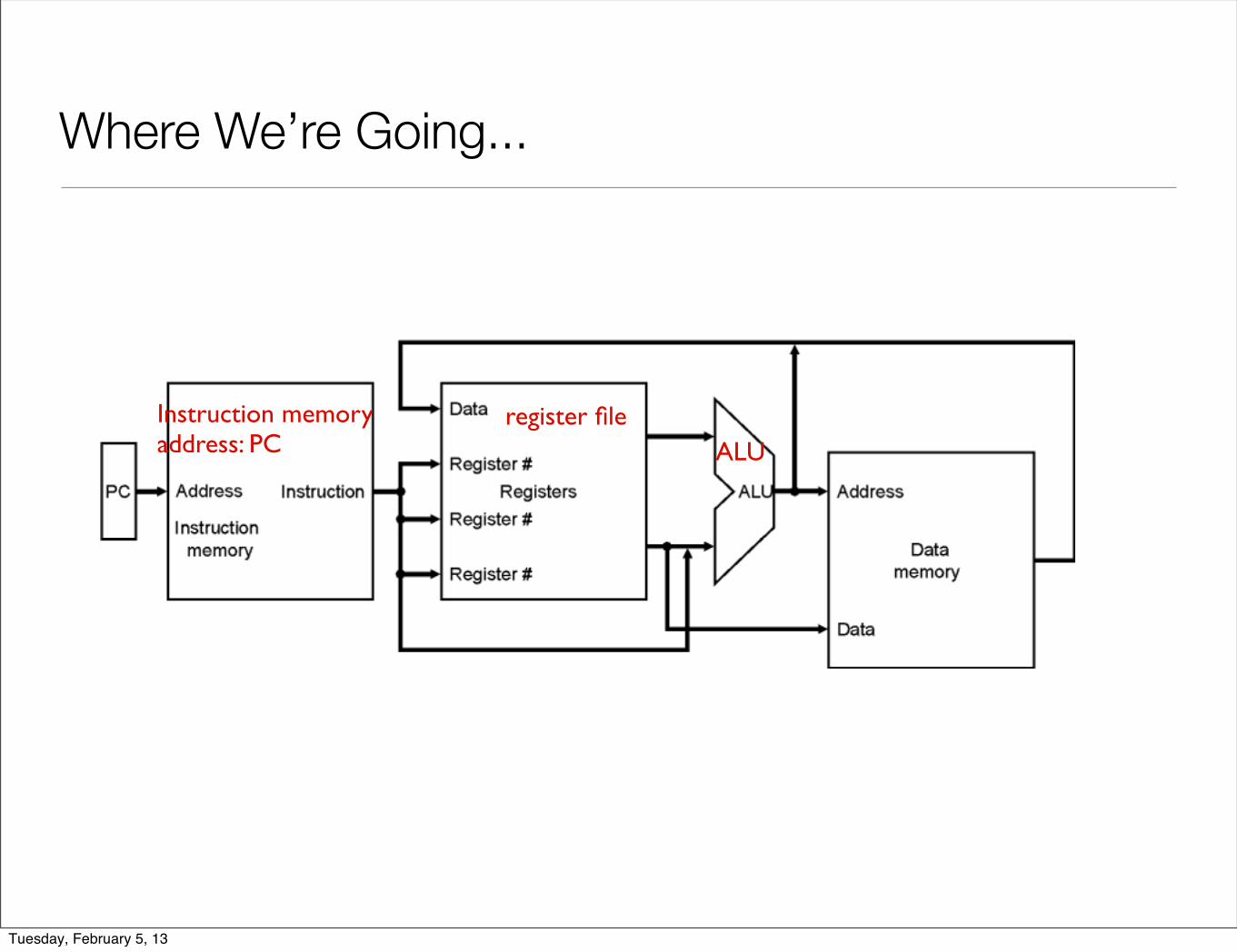
Where We’re Going...
Instruction memoryaddress: PC
register fileALU
Tuesday, February 5, 13
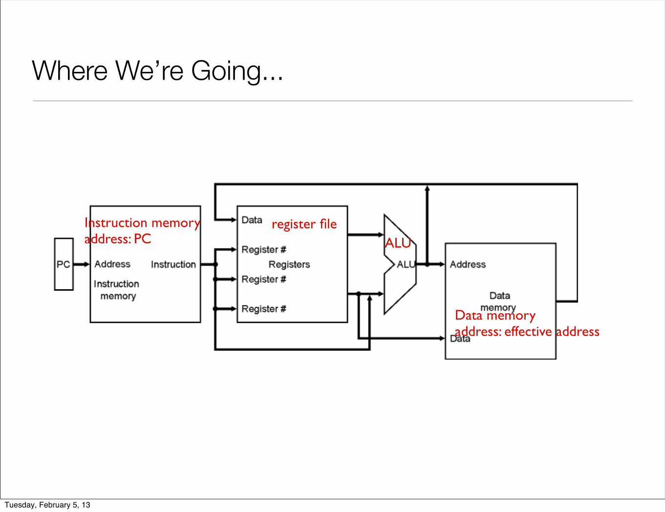
Where We’re Going...
Instruction memoryaddress: PC
register fileALU
Data memoryaddress: effective address
Tuesday, February 5, 13

Where We’re Going...
Instruction memoryaddress: PC
register fileALU
Data memoryaddress: effective address
program counter
Tuesday, February 5, 13
Review: Two Type of Logical Components
Tuesday, February 5, 13
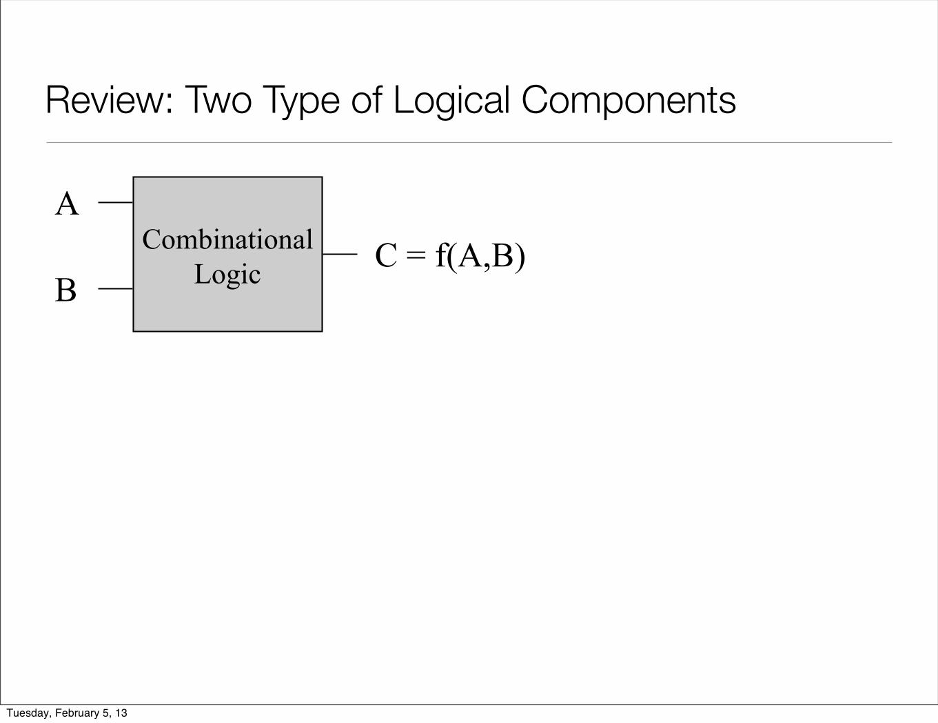
Review: Two Type of Logical Components
Combinational Logic
A
B C = f(A,B)
Tuesday, February 5, 13
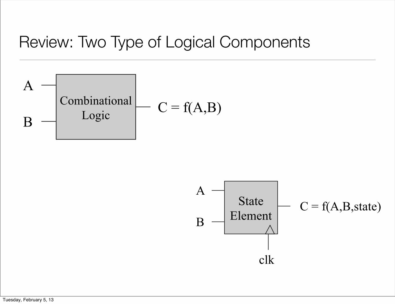
Review: Two Type of Logical Components
State Element
clk
A
B C = f(A,B,state)
Combinational Logic
A
B C = f(A,B)
Tuesday, February 5, 13
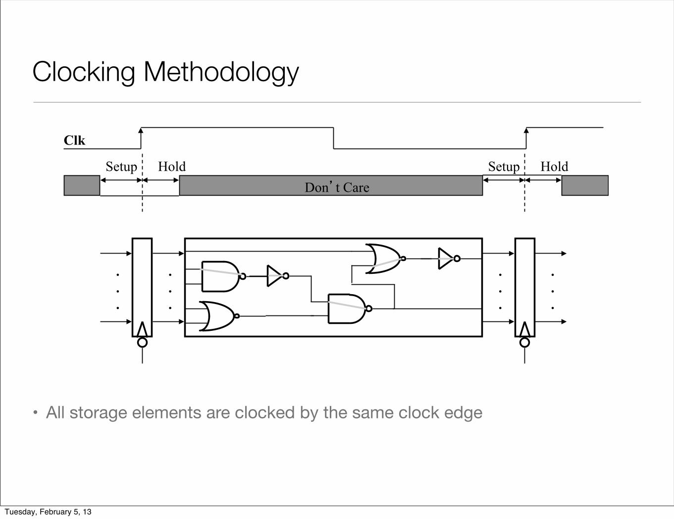
Clocking Methodology
• All storage elements are clocked by the same clock edge
Clk
Don�t Care Setup Hold
.
.
.
.
.
.
.
.
.
.
.
.
Setup Hold
Tuesday, February 5, 13
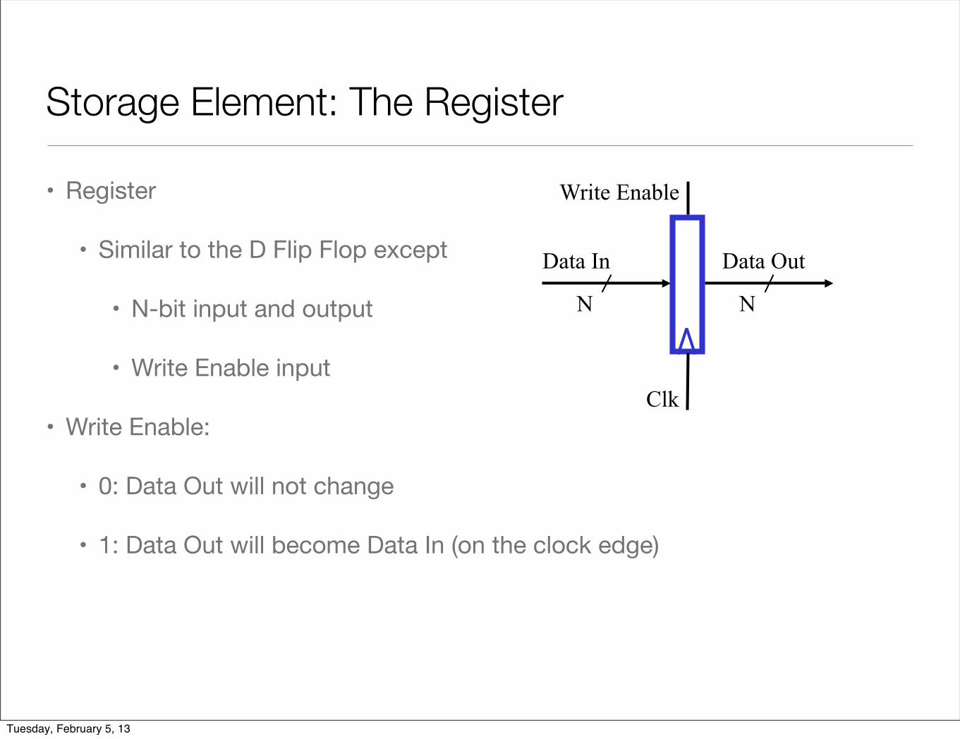
Storage Element: The Register
• Register
• Similar to the D Flip Flop except
• N-bit input and output
• Write Enable input
• Write Enable:
• 0: Data Out will not change
• 1: Data Out will become Data In (on the clock edge)
Clk
Data In
Write Enable
N N
Data Out
Tuesday, February 5, 13
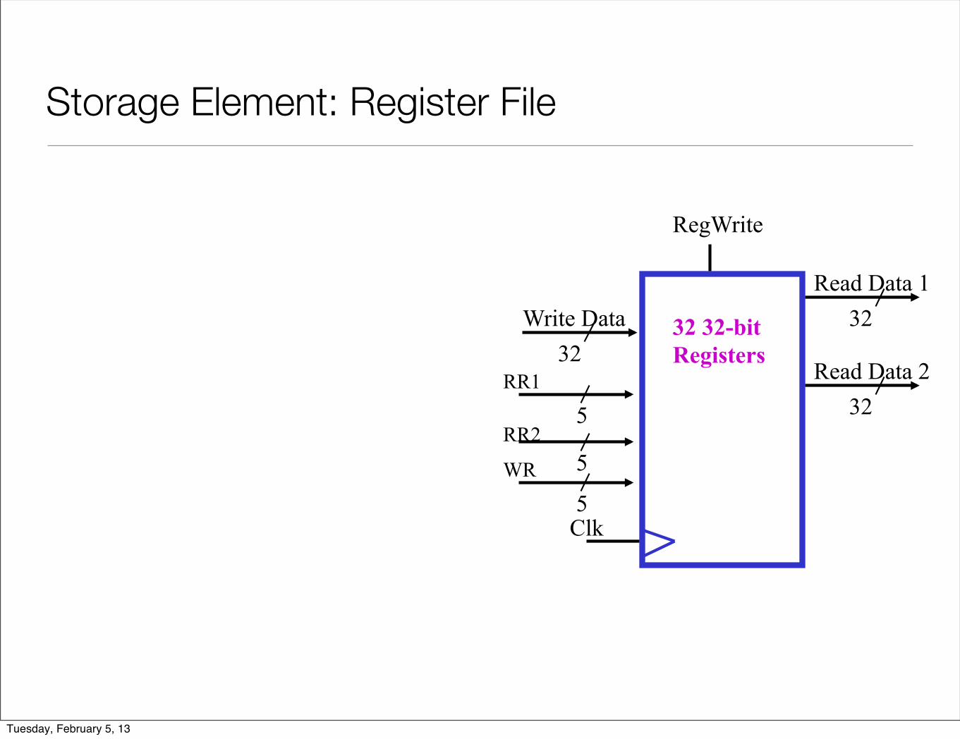
Storage Element: Register File
Clk
Write Data
RegWrite
32 32
Read Data 1
32 Read Data 2
32 32-bit Registers
5
5
5
RR1
RR2
WR
Tuesday, February 5, 13
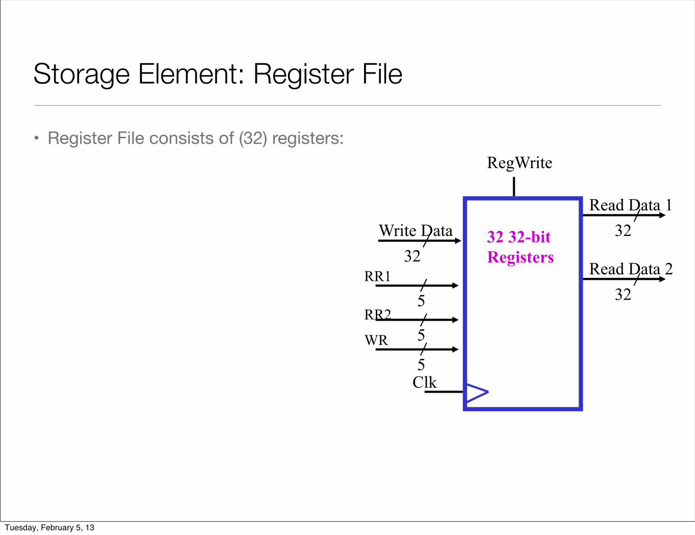
Storage Element: Register File
• Register File consists of (32) registers:
Clk
Write Data
RegWrite
32 32
Read Data 1
32 Read Data 2
32 32-bit Registers
5
5
5
RR1
RR2
WR
Tuesday, February 5, 13
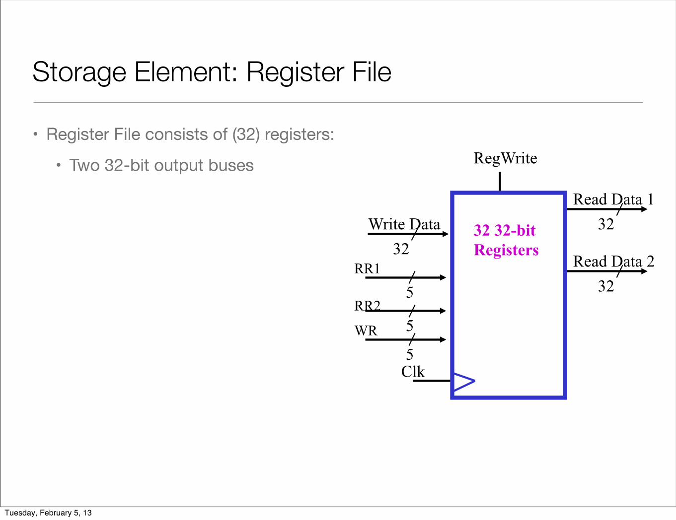
Storage Element: Register File
• Register File consists of (32) registers:
• Two 32-bit output buses
Clk
Write Data
RegWrite
32 32
Read Data 1
32 Read Data 2
32 32-bit Registers
5
5
5
RR1
RR2
WR
Tuesday, February 5, 13

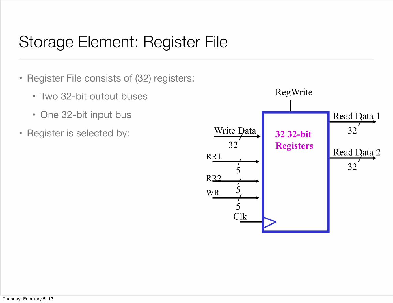
Storage Element: Register File
• Register File consists of (32) registers:
• Two 32-bit output buses
• One 32-bit input bus
Clk
Write Data
RegWrite
32 32
Read Data 1
32 Read Data 2
32 32-bit Registers
5
5
5
RR1
RR2
WR
Tuesday, February 5, 13
Storage Element: Register File
• Register File consists of (32) registers:
• Two 32-bit output buses
• One 32-bit input bus
• Register is selected by:
Clk
Write Data
RegWrite
32 32
Read Data 1
32 Read Data 2
32 32-bit Registers
5
5
5
RR1
RR2
WR
Tuesday, February 5, 13
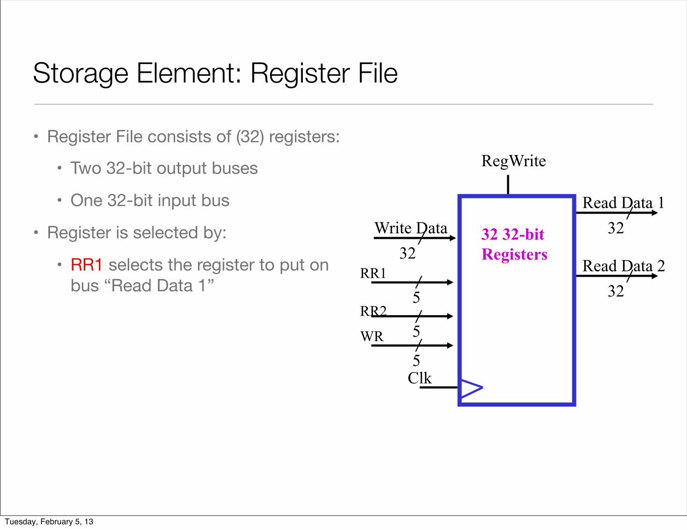
Storage Element: Register File
• Register File consists of (32) registers:
• Two 32-bit output buses
• One 32-bit input bus
• Register is selected by:
• RR1 selects the register to put on bus “Read Data 1”
Clk
Write Data
RegWrite
32 32
Read Data 1
32 Read Data 2
32 32-bit Registers
5
5
5
RR1
RR2
WR
Tuesday, February 5, 13
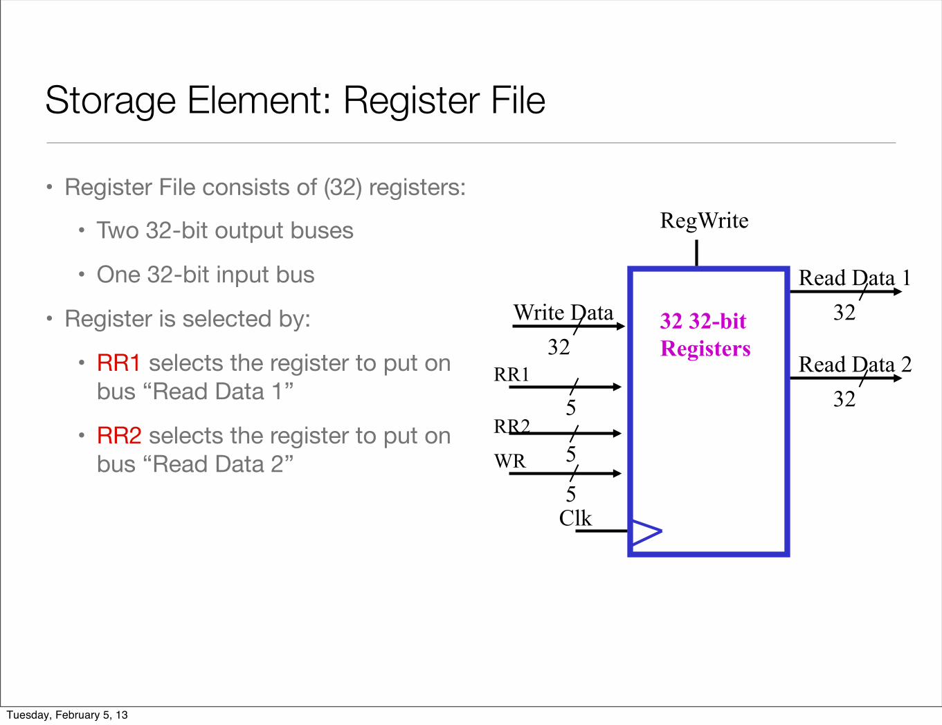
Storage Element: Register File
• Register File consists of (32) registers:
• Two 32-bit output buses
• One 32-bit input bus
• Register is selected by:
• RR1 selects the register to put on bus “Read Data 1”
• RR2 selects the register to put on bus “Read Data 2”
Clk
Write Data
RegWrite
32 32
Read Data 1
32 Read Data 2
32 32-bit Registers
5
5
5
RR1
RR2
WR
Tuesday, February 5, 13
Storage Element: Register File
• Register File consists of (32) registers:
• Two 32-bit output buses
• One 32-bit input bus
• Register is selected by:
• RR1 selects the register to put on bus “Read Data 1”
• RR2 selects the register to put on bus “Read Data 2”
• WR selects the register to be written
Clk
Write Data
RegWrite
32 32
Read Data 1
32 Read Data 2
32 32-bit Registers
5
5
5
RR1
RR2
WR
Tuesday, February 5, 13

Storage Element: Register File
• Register File consists of (32) registers:
• Two 32-bit output buses
• One 32-bit input bus
• Register is selected by:
• RR1 selects the register to put on bus “Read Data 1”
• RR2 selects the register to put on bus “Read Data 2”
• WR selects the register to be written
• via WriteData when RegWrite is 1
Clk
Write Data
RegWrite
32 32
Read Data 1
32 Read Data 2
32 32-bit Registers
5
5
5
RR1
RR2
WR
Tuesday, February 5, 13
Storage Element: Register File
• Register File consists of (32) registers:
• Two 32-bit output buses
• One 32-bit input bus
• Register is selected by:
• RR1 selects the register to put on bus “Read Data 1”
• RR2 selects the register to put on bus “Read Data 2”
• WR selects the register to be written
• via WriteData when RegWrite is 1
• Clock input (CLK)
Clk
Write Data
RegWrite
32 32
Read Data 1
32 Read Data 2
32 32-bit Registers
5
5
5
RR1
RR2
WR
Tuesday, February 5, 13
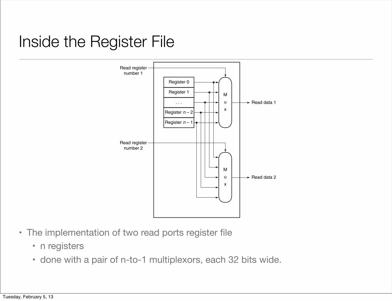
Inside the Register File
• The implementation of two read ports register file• n registers • done with a pair of n-to-1 multiplexors, each 32 bits wide.
C.8 Memory Elements: Flip-Flops, Latches, and Registers C-55
FIGURE C.8.7 A register fi le with two read ports and one write port has fi ve inputs and two outputs. The control input Write is shown in color.
FIGURE C.8.8 The implementation of two read ports for a register fi le with n registers can be done with a pair of n-to-1 multiplexors, each 32 bits wide. The register read number sig nal is used as the multiplexor selector signal. Figure C.8.9 shows how the write port is implemented.
Read registernumber 1 Read
data 1Read registernumber 2
Read data 2
Writeregister
WriteWritedata
Register file
Read registernumber 1
Register 0
Register 1
. . .
Register n – 2
Register n – 1
M
u
x
Read registernumber 2
M
u
x
Read data 1
Read data 2
AppendixC-9780123747501.indd 55AppendixC-9780123747501.indd 55 26/07/11 6:29 PM26/07/11 6:29 PM
Tuesday, February 5, 13
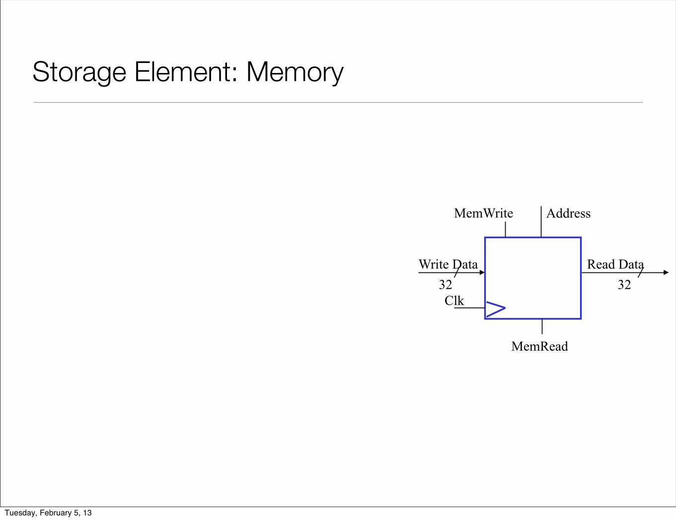
Storage Element: Memory
Clk
Write Data
MemWrite
32 32 Read Data
Address
MemRead
Tuesday, February 5, 13
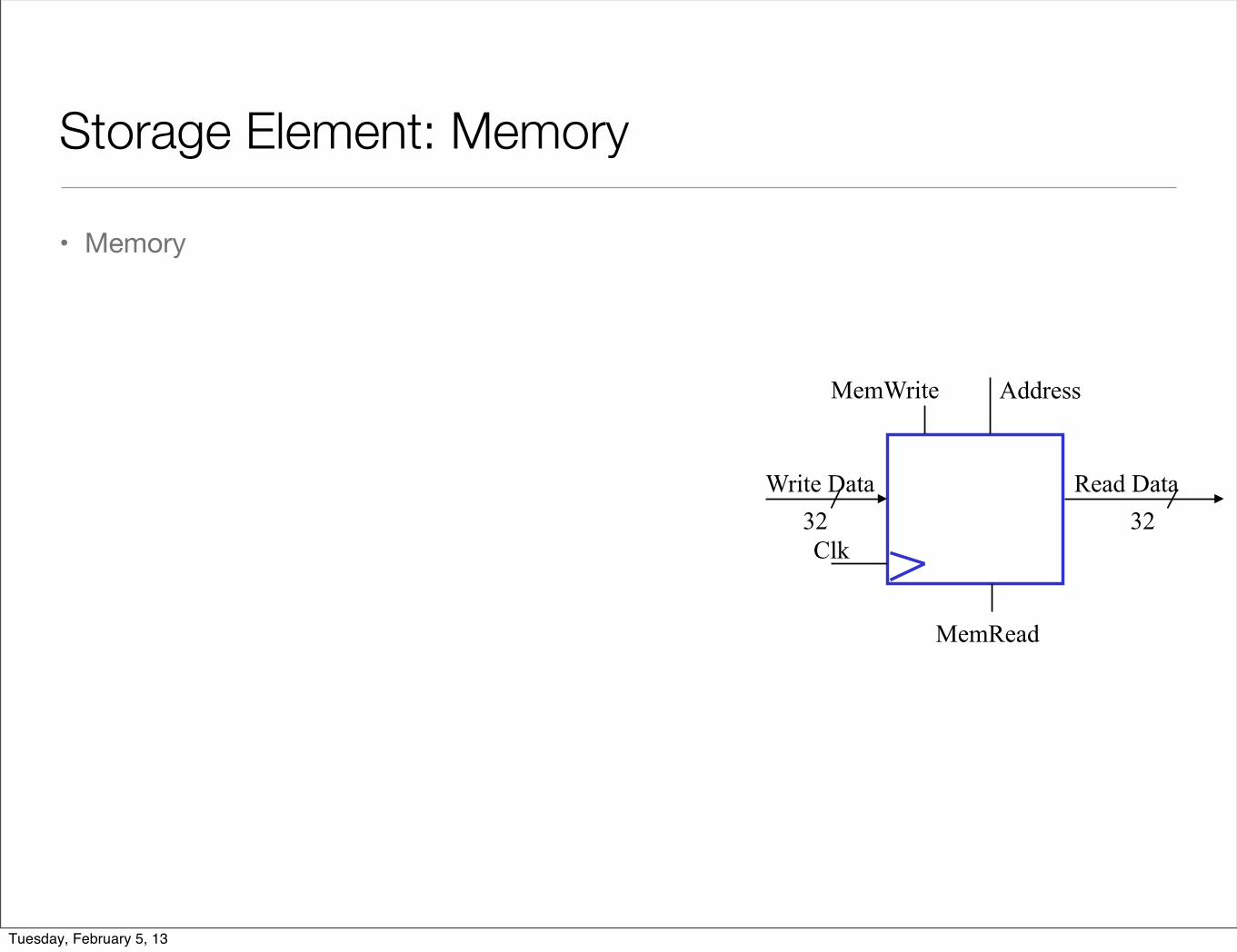
Storage Element: Memory
• Memory
Clk
Write Data
MemWrite
32 32 Read Data
Address
MemRead
Tuesday, February 5, 13
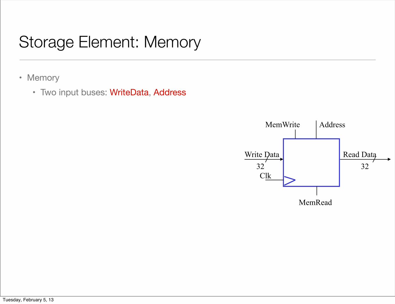
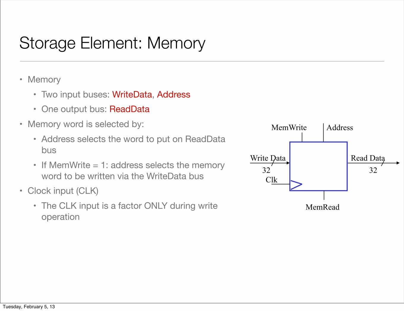
Storage Element: Memory
• Memory• Two input buses: WriteData, Address
Clk
Write Data
MemWrite
32 32 Read Data
Address
MemRead
Tuesday, February 5, 13
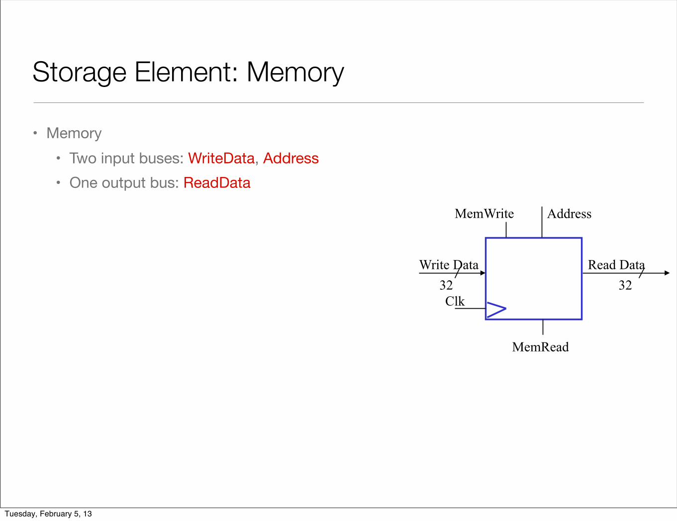
Storage Element: Memory
• Memory• Two input buses: WriteData, Address• One output bus: ReadData
Clk
Write Data
MemWrite
32 32 Read Data
Address
MemRead
Tuesday, February 5, 13
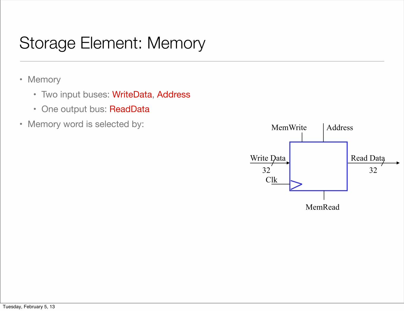
Storage Element: Memory
• Memory• Two input buses: WriteData, Address• One output bus: ReadData
• Memory word is selected by:
Clk
Write Data
MemWrite
32 32 Read Data
Address
MemRead
Tuesday, February 5, 13
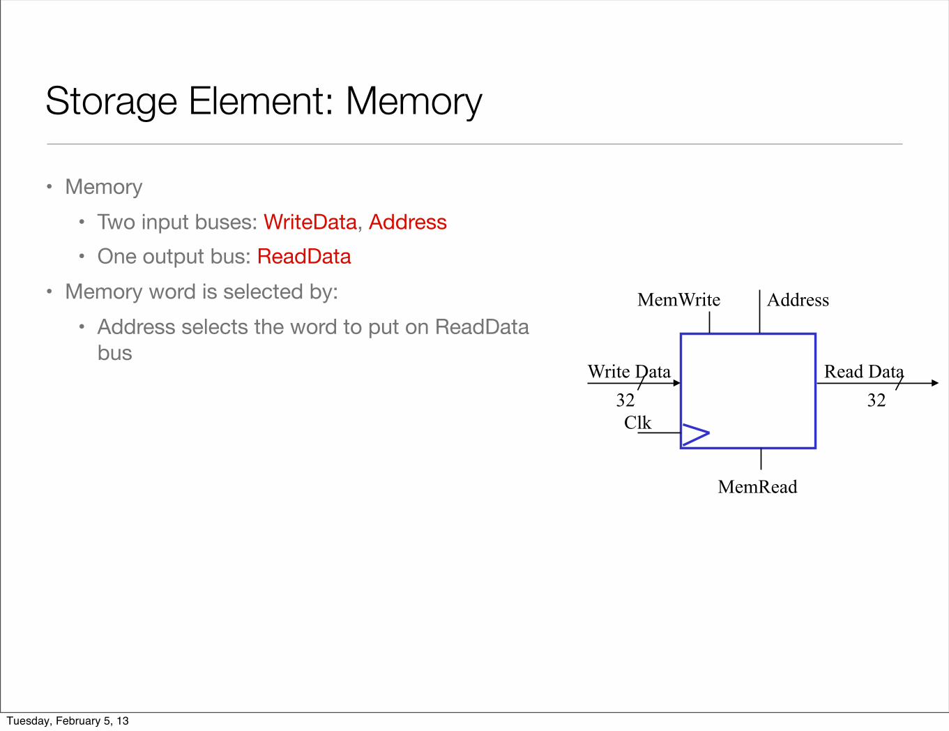
Storage Element: Memory
• Memory• Two input buses: WriteData, Address• One output bus: ReadData
• Memory word is selected by:• Address selects the word to put on ReadData
bus
Clk
Write Data
MemWrite
32 32 Read Data
Address
MemRead
Tuesday, February 5, 13
Storage Element: Memory
• Memory• Two input buses: WriteData, Address• One output bus: ReadData
• Memory word is selected by:• Address selects the word to put on ReadData
bus• If MemWrite = 1: address selects the memory
word to be written via the WriteData bus Clk
Write Data
MemWrite
32 32 Read Data
Address
MemRead
Tuesday, February 5, 13
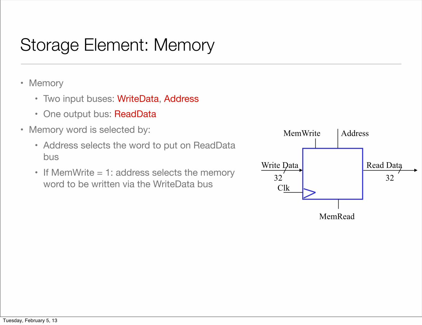
Storage Element: Memory
• Memory• Two input buses: WriteData, Address• One output bus: ReadData
• Memory word is selected by:• Address selects the word to put on ReadData
bus• If MemWrite = 1: address selects the memory
word to be written via the WriteData bus• Clock input (CLK)
Clk
Write Data
MemWrite
32 32 Read Data
Address
MemRead
Tuesday, February 5, 13
Storage Element: Memory
• Memory• Two input buses: WriteData, Address• One output bus: ReadData
• Memory word is selected by:• Address selects the word to put on ReadData
bus• If MemWrite = 1: address selects the memory
word to be written via the WriteData bus• Clock input (CLK)
• The CLK input is a factor ONLY during write operation
Clk
Write Data
MemWrite
32 32 Read Data
Address
MemRead
Tuesday, February 5, 13
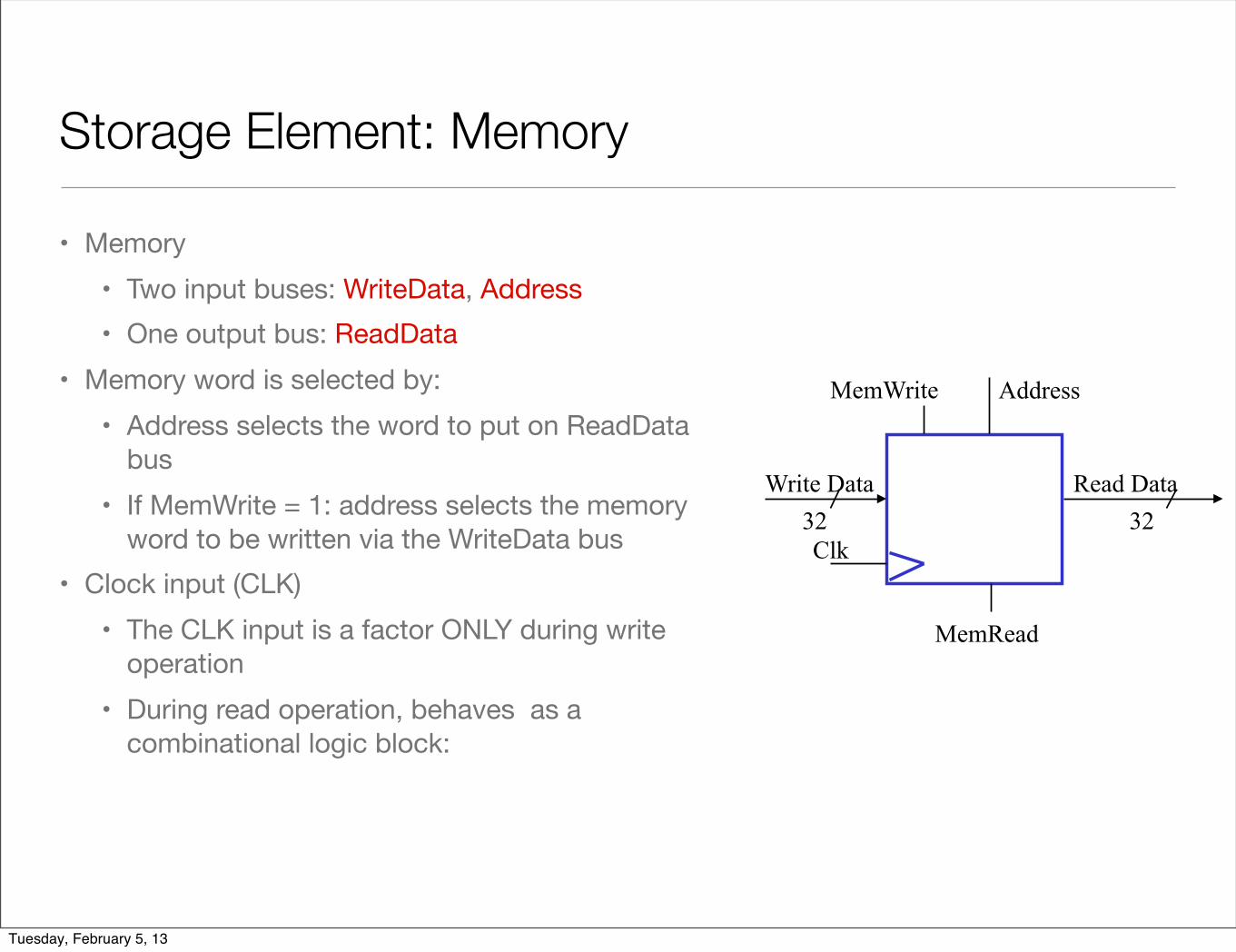
Storage Element: Memory
• Memory• Two input buses: WriteData, Address• One output bus: ReadData
• Memory word is selected by:• Address selects the word to put on ReadData
bus• If MemWrite = 1: address selects the memory
word to be written via the WriteData bus• Clock input (CLK)
• The CLK input is a factor ONLY during write operation
• During read operation, behaves as a combinational logic block:
Clk
Write Data
MemWrite
32 32 Read Data
Address
MemRead
Tuesday, February 5, 13
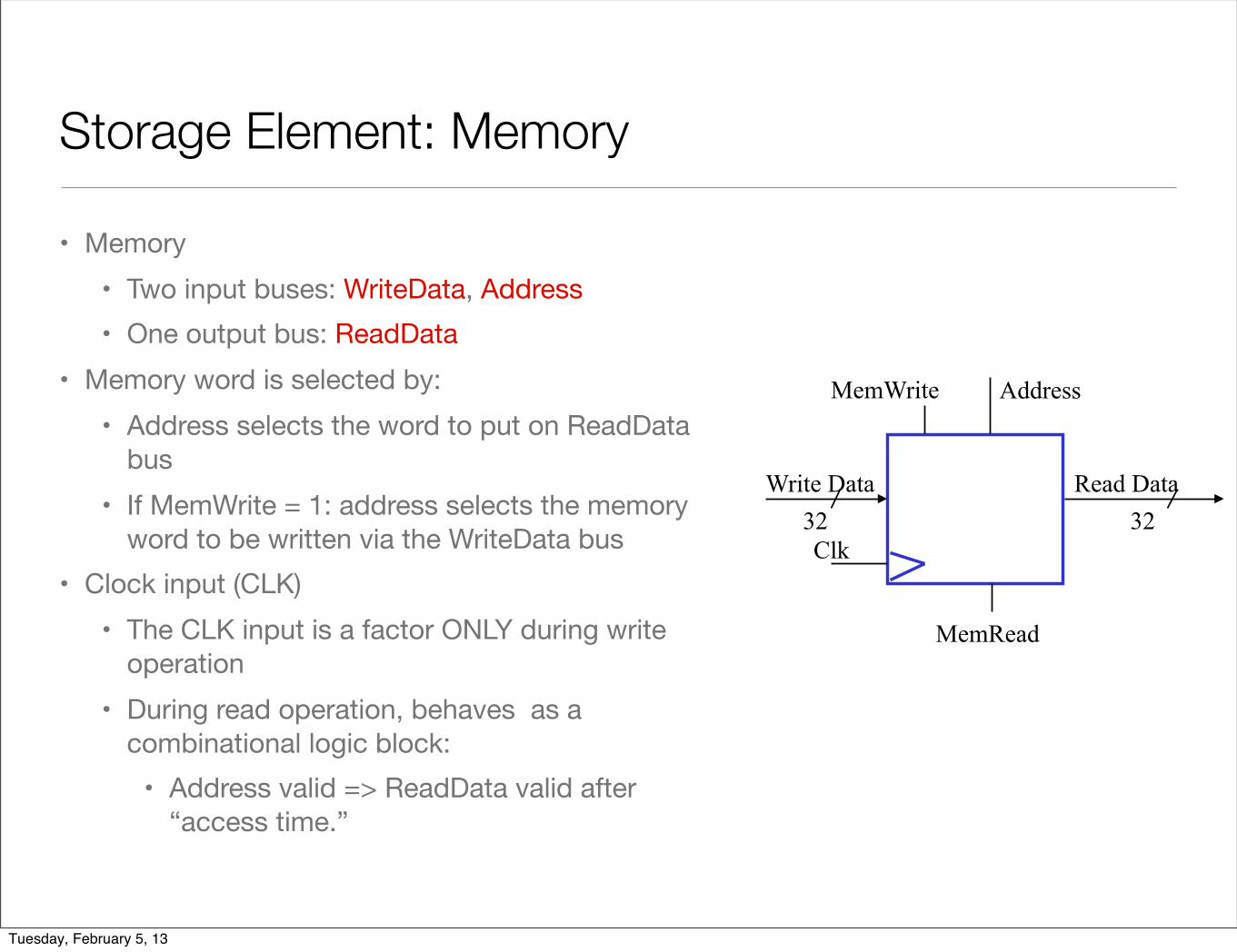
Storage Element: Memory
• Memory• Two input buses: WriteData, Address• One output bus: ReadData
• Memory word is selected by:• Address selects the word to put on ReadData
bus• If MemWrite = 1: address selects the memory
word to be written via the WriteData bus• Clock input (CLK)
• The CLK input is a factor ONLY during write operation
• During read operation, behaves as a combinational logic block:• Address valid => ReadData valid after
“access time.”
Clk
Write Data
MemWrite
32 32 Read Data
Address
MemRead
Tuesday, February 5, 13
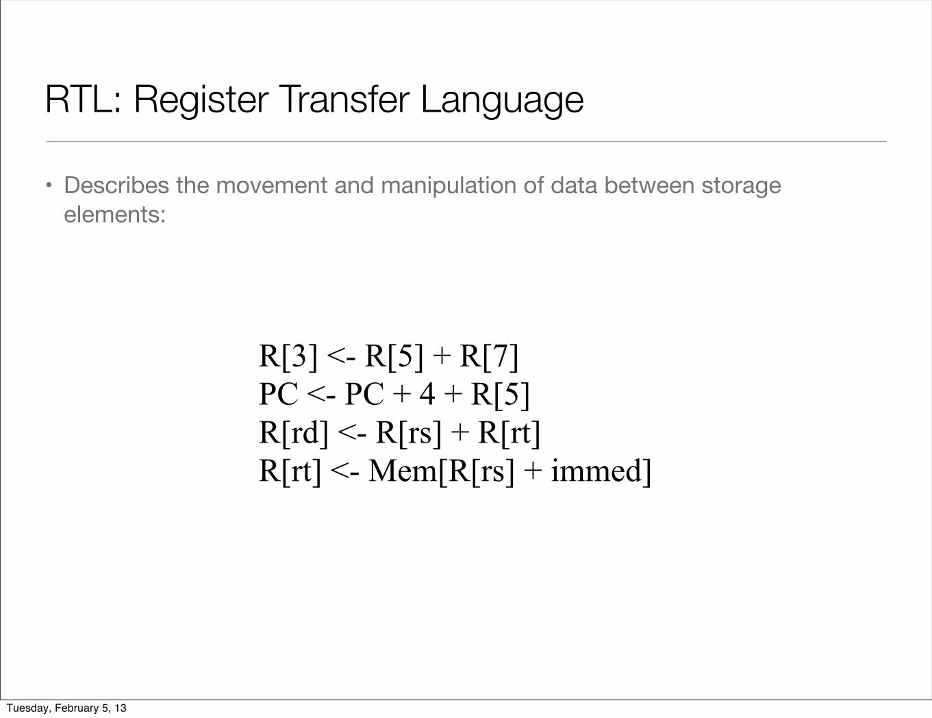
RTL: Register Transfer Language
• Describes the movement and manipulation of data between storage elements:
R[3] <- R[5] + R[7]PC <- PC + 4 + R[5]R[rd] <- R[rs] + R[rt]R[rt] <- Mem[R[rs] + immed]
Tuesday, February 5, 13
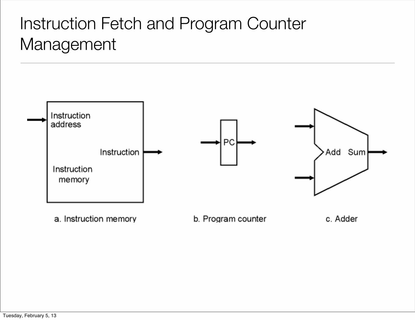
Instruction Fetch and Program Counter Management
Tuesday, February 5, 13
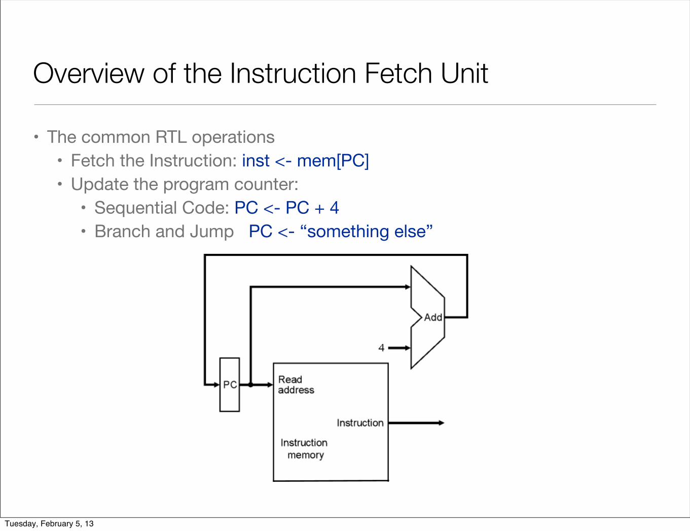
Overview of the Instruction Fetch Unit
• The common RTL operations• Fetch the Instruction: inst <- mem[PC]• Update the program counter:
• Sequential Code: PC <- PC + 4 • Branch and Jump PC <- “something else”
Tuesday, February 5, 13
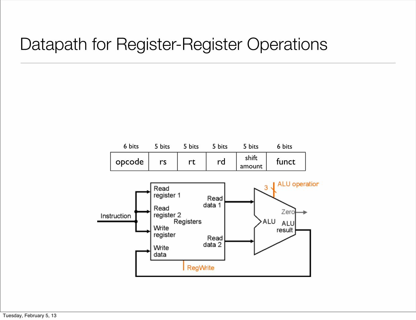
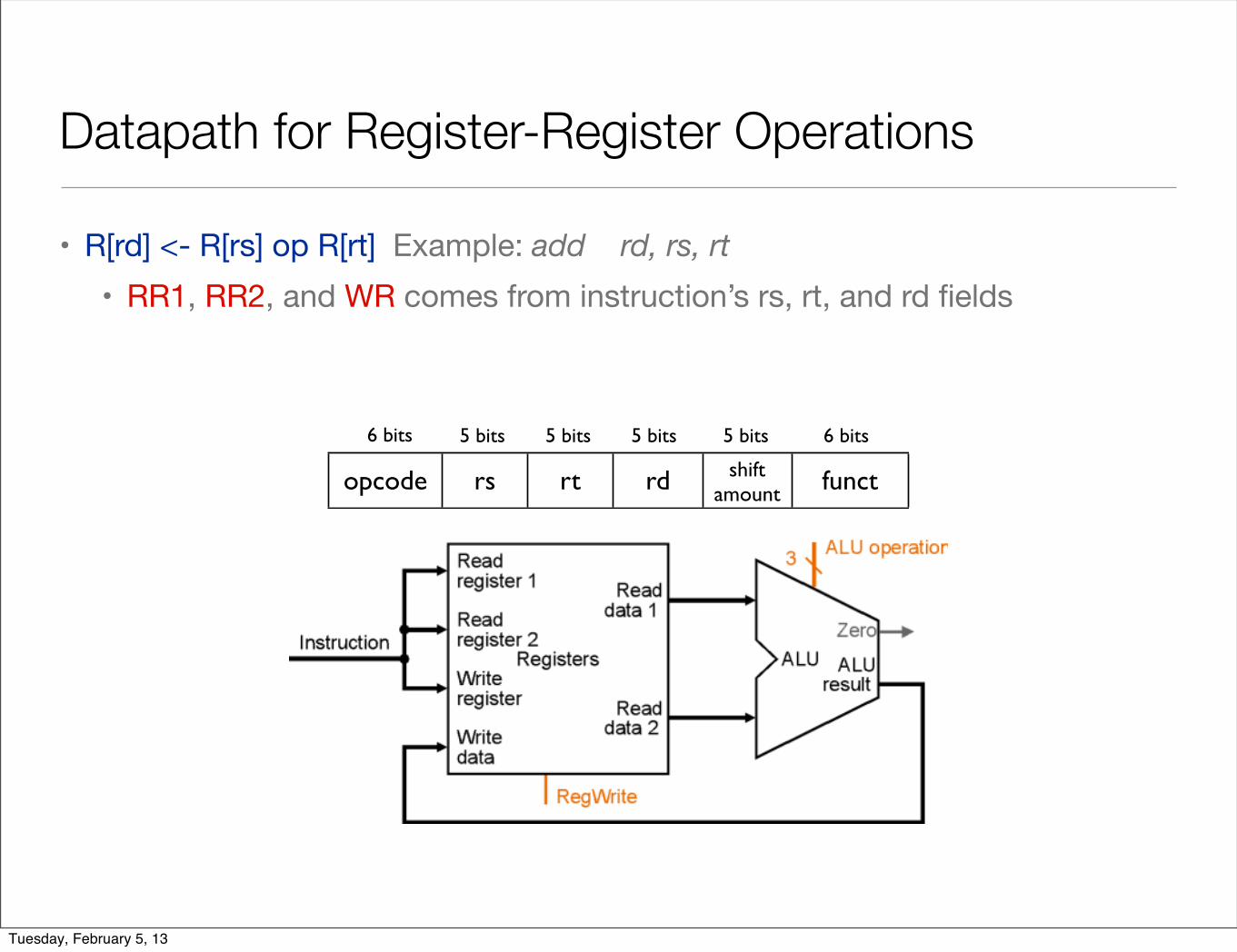
Datapath for Register-Register Operations
opcode rs rt rd shift amount funct
6 bits 5 bits 5 bits 5 bits 5 bits 6 bits
Tuesday, February 5, 13
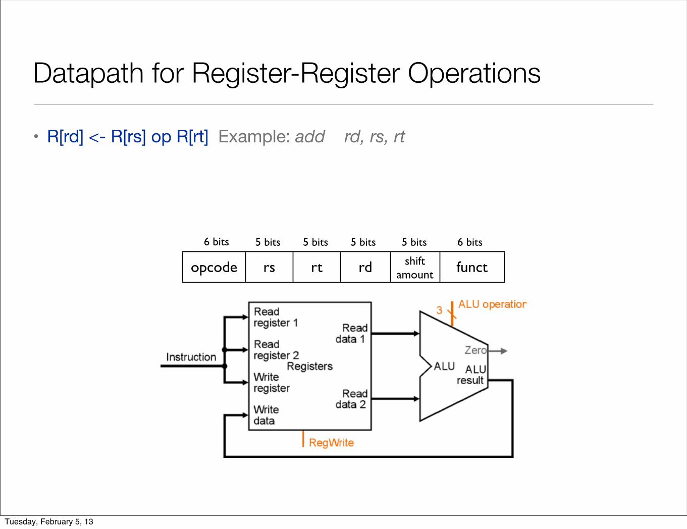
Datapath for Register-Register Operations
• R[rd] <- R[rs] op R[rt] Example: add rd, rs, rt
opcode rs rt rd shift amount funct
6 bits 5 bits 5 bits 5 bits 5 bits 6 bits
Tuesday, February 5, 13
Datapath for Register-Register Operations
• R[rd] <- R[rs] op R[rt] Example: add rd, rs, rt• RR1, RR2, and WR comes from instruction’s rs, rt, and rd fields
opcode rs rt rd shift amount funct
6 bits 5 bits 5 bits 5 bits 5 bits 6 bits
Tuesday, February 5, 13
Datapath for Register-Register Operations
• R[rd] <- R[rs] op R[rt] Example: add rd, rs, rt• RR1, RR2, and WR comes from instruction’s rs, rt, and rd fields• ALUoperation and RegWrite: control logic after decoding instruction
opcode rs rt rd shift amount funct
6 bits 5 bits 5 bits 5 bits 5 bits 6 bits
Tuesday, February 5, 13

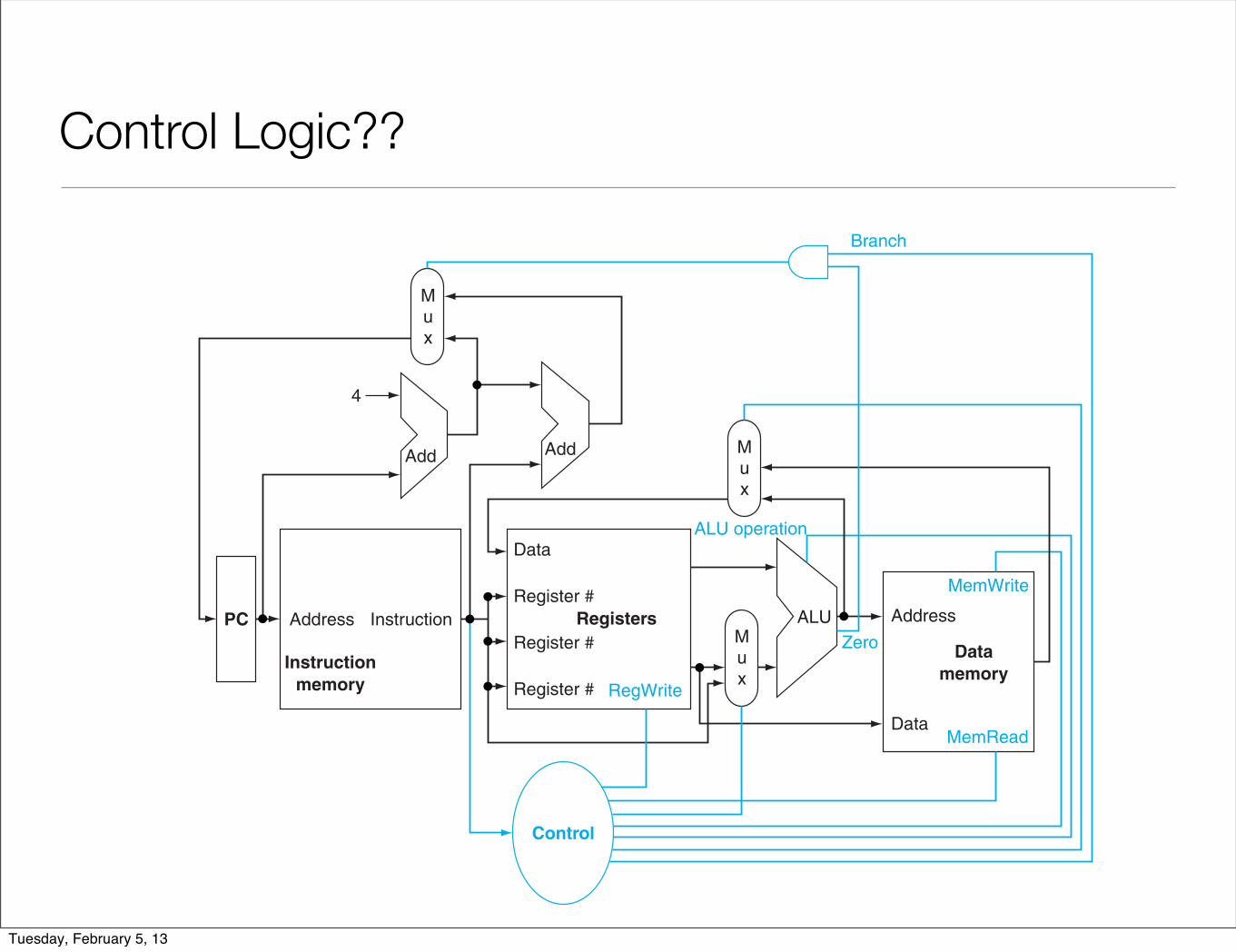
Control Logic??288 Chapter 5 The Processor: Datapath and Control
While easier to understand, this approach is not practical, since it would beslower than an implementation that allows different instruction classes to take dif-ferent numbers of clock cycles, each of which could be much shorter. After design-ing the control for this simple machine, we will look at an implementation thatuses multiple clock cycles for each instruction. This multicycle design is used
FIGURE 5.2 The basic implementation of the MIPS subset including the necessary multiplexors and controllines. The top multiplexor controls what value replaces the PC (PC + 4 or the branch destination address); the multiplexor is con-trolled by the gate that “ands” together the Zero output of the ALU and a control signal that indicates that the instruction is abranch. The multiplexor whose output returns to the register file is used to steer the output of the ALU (in the case of an arithmetic-logical instruction) or the output of the data memory (in the case of a load) for writing into the register file. Finally, the bottommostmultiplexor is used to determine whether the second ALU input is from the registers (for a nonimmediate arithmetic-logicalinstruction) or from the offset field of the instruction (for an immediate operation, a load or store, or a branch). The added controllines are straightforward and determine the operation performed at the ALU, whether the data memory should read or write, andwhether the registers should perform a write operation. The control lines are shown in color to make them easier to see.
Data
Register #
Register #
Register #
PC Address Instruction
Instructionmemory
Registers ALU Address
Data
Datamemory
AddAdd
4
MemWrite
MemRead
Mux
Mux
Mux
Control
RegWrite
Zero
Branch
ALU operation
Tuesday, February 5, 13
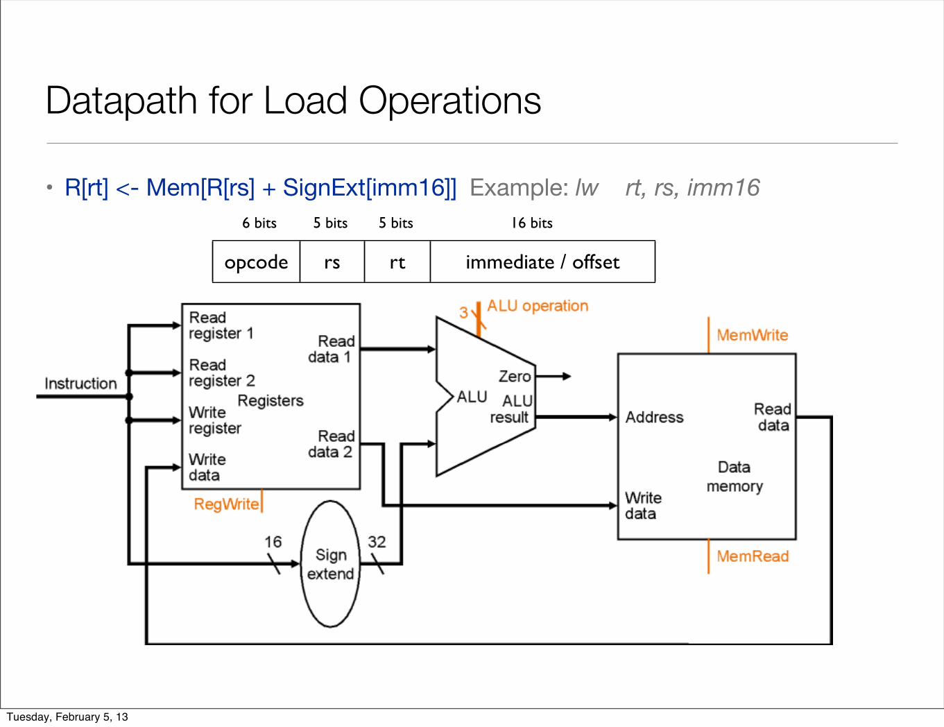
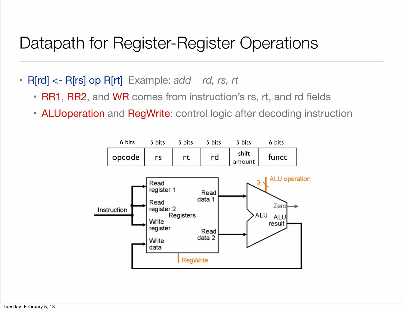
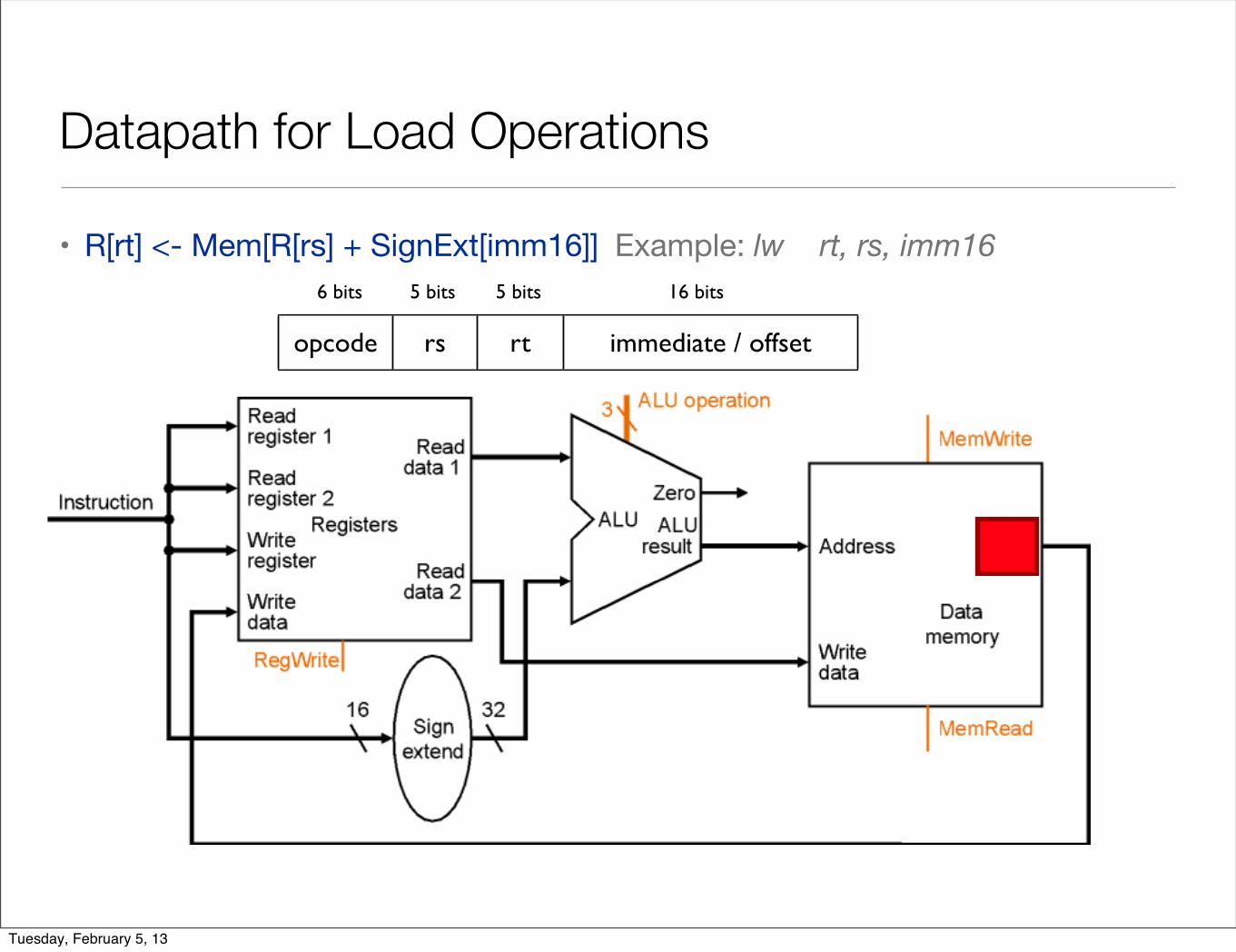
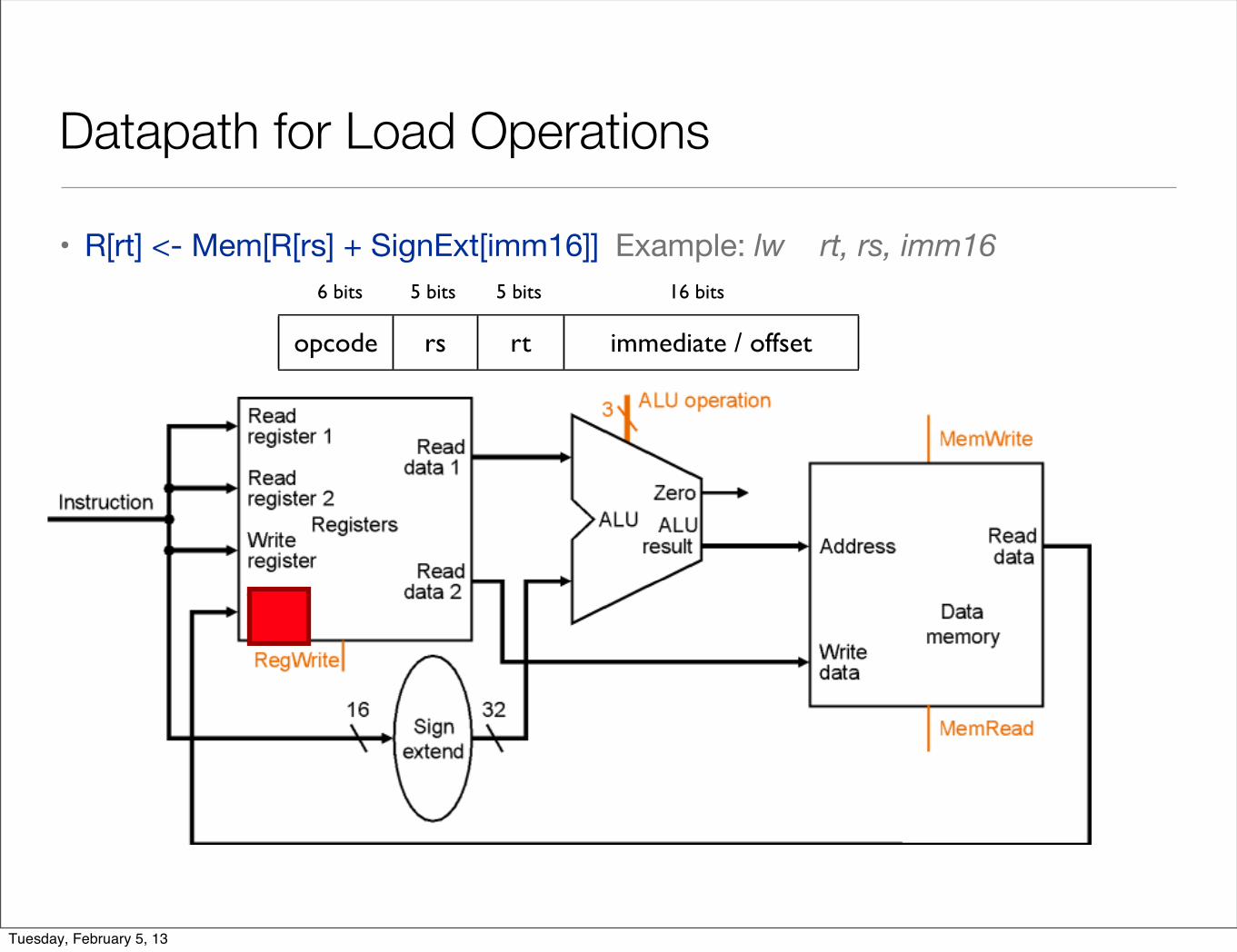
Datapath for Load Operations
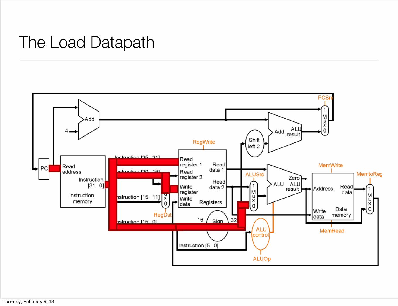
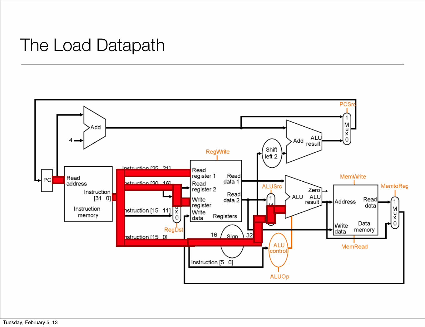
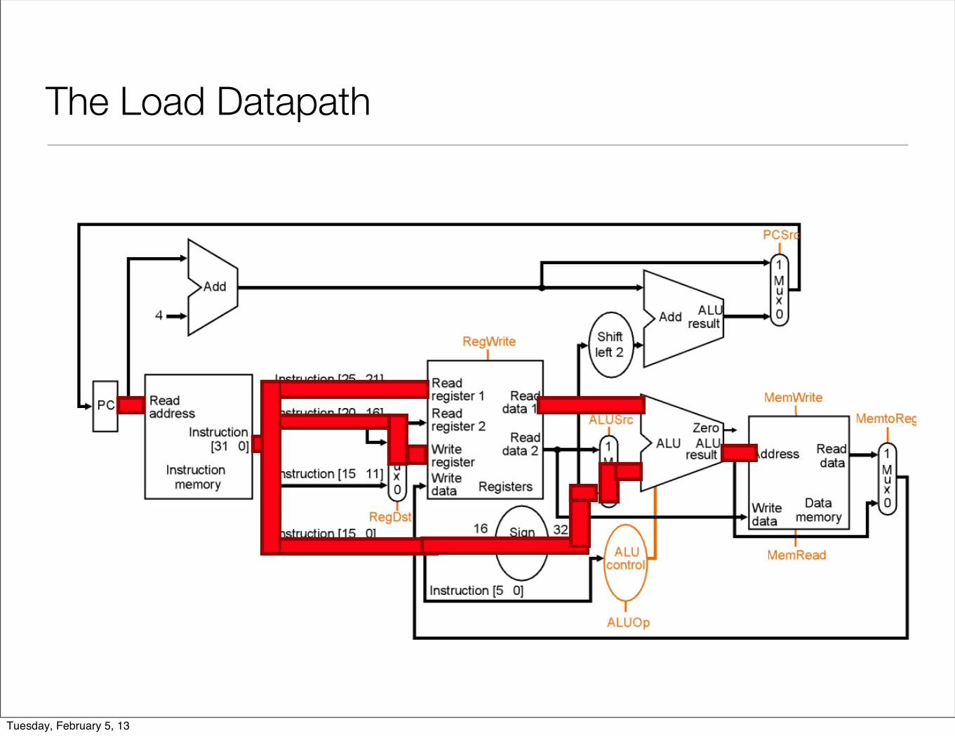
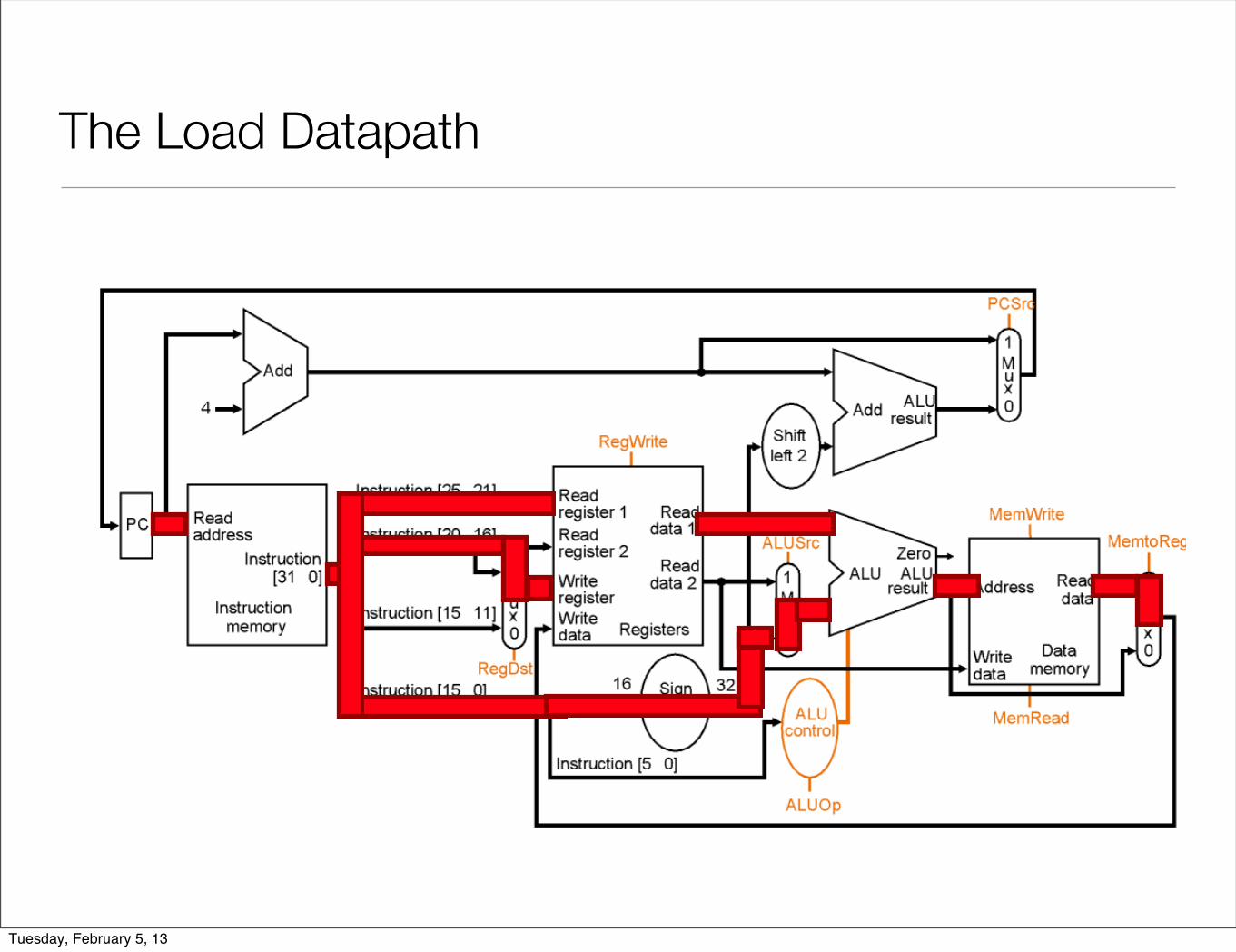
• R[rt] <- Mem[R[rs] + SignExt[imm16]] Example: lw rt, rs, imm16
opcode rs rt immediate / offset
6 bits 5 bits 5 bits 16 bits
Tuesday, February 5, 13
Datapath for Load Operations
• R[rt] <- Mem[R[rs] + SignExt[imm16]] Example: lw rt, rs, imm16
opcode rs rt immediate / offset
6 bits 5 bits 5 bits 16 bits
Tuesday, February 5, 13
Datapath for Load Operations
• R[rt] <- Mem[R[rs] + SignExt[imm16]] Example: lw rt, rs, imm16
opcode rs rt immediate / offset
6 bits 5 bits 5 bits 16 bits
Tuesday, February 5, 13
Datapath for Load Operations
• R[rt] <- Mem[R[rs] + SignExt[imm16]] Example: lw rt, rs, imm16
opcode rs rt immediate / offset
6 bits 5 bits 5 bits 16 bits
Tuesday, February 5, 13
Datapath for Load Operations
• R[rt] <- Mem[R[rs] + SignExt[imm16]] Example: lw rt, rs, imm16
opcode rs rt immediate / offset
6 bits 5 bits 5 bits 16 bits
Tuesday, February 5, 13
Datapath for Load Operations
• R[rt] <- Mem[R[rs] + SignExt[imm16]] Example: lw rt, rs, imm16
opcode rs rt immediate / offset
6 bits 5 bits 5 bits 16 bits
Tuesday, February 5, 13

Datapath for Load Operations
• R[rt] <- Mem[R[rs] + SignExt[imm16]] Example: lw rt, rs, imm16
opcode rs rt immediate / offset
6 bits 5 bits 5 bits 16 bits
Tuesday, February 5, 13
Datapath for Load Operations
• R[rt] <- Mem[R[rs] + SignExt[imm16]] Example: lw rt, rs, imm16
opcode rs rt immediate / offset
6 bits 5 bits 5 bits 16 bits
Tuesday, February 5, 13
Datapath for Load Operations
• R[rt] <- Mem[R[rs] + SignExt[imm16]] Example: lw rt, rs, imm16
opcode rs rt immediate / offset
6 bits 5 bits 5 bits 16 bits
Tuesday, February 5, 13

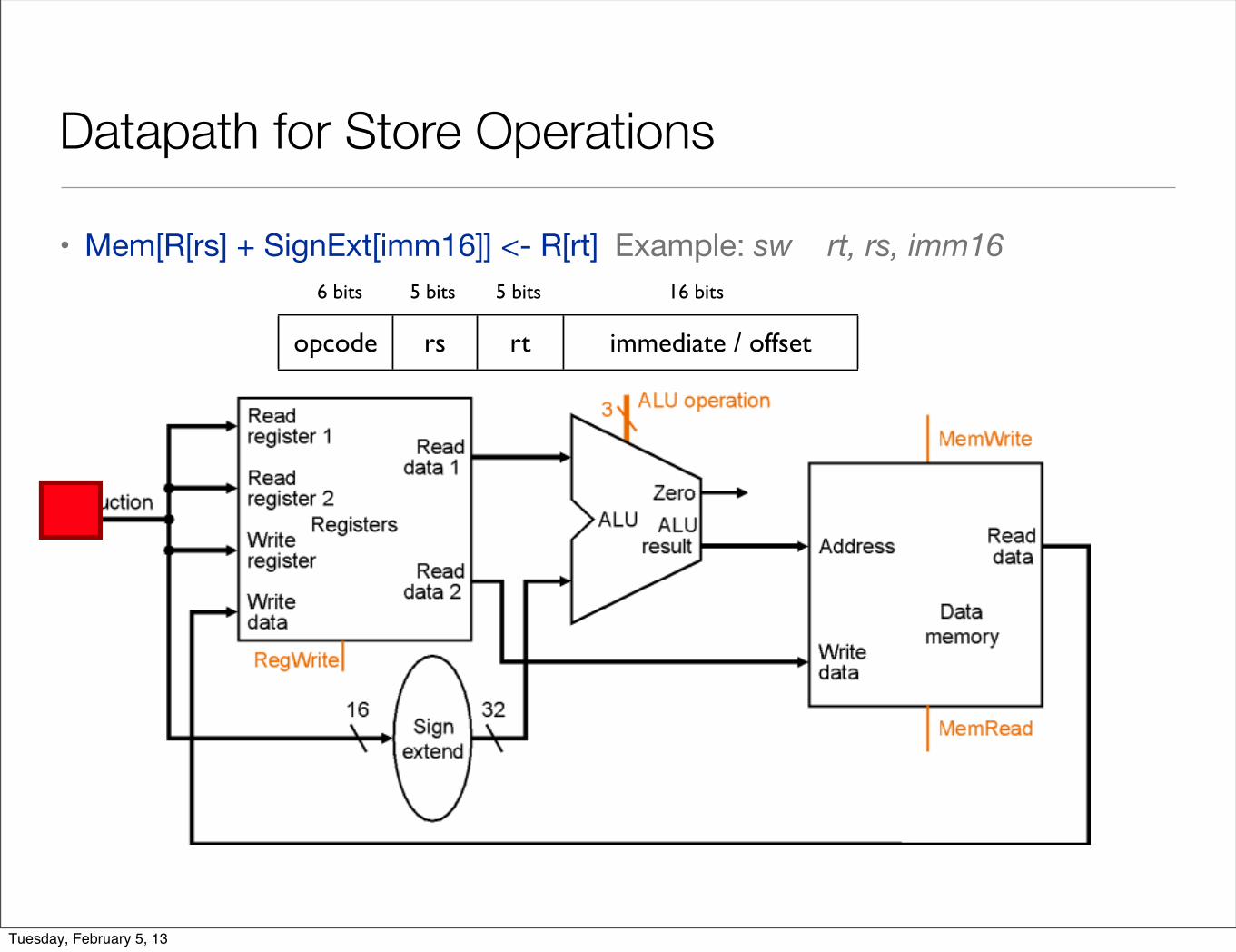
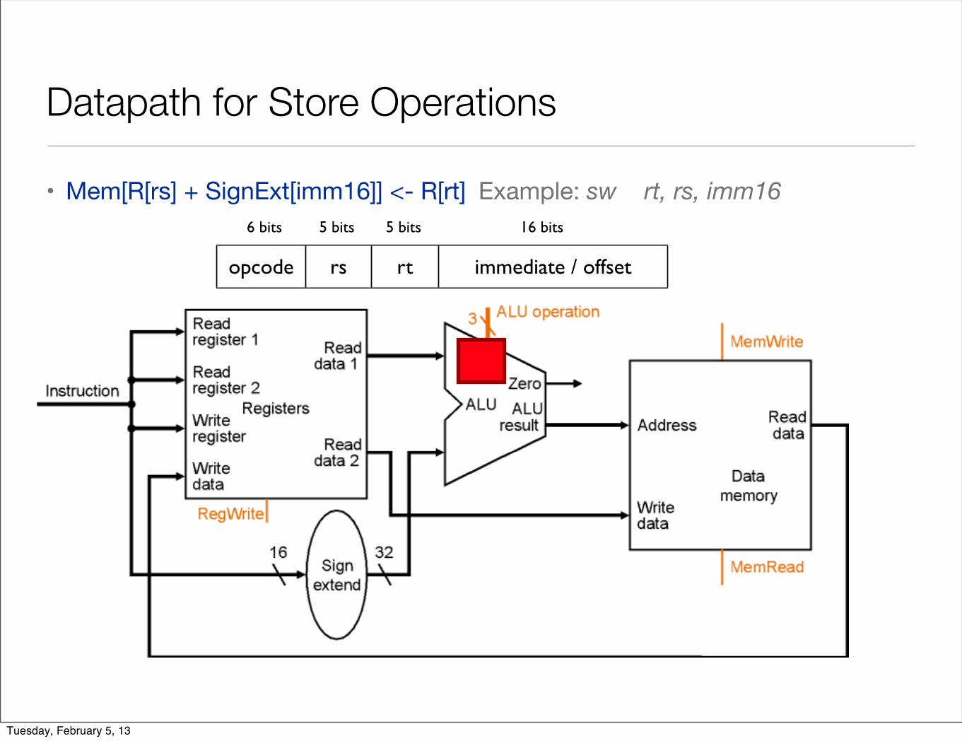
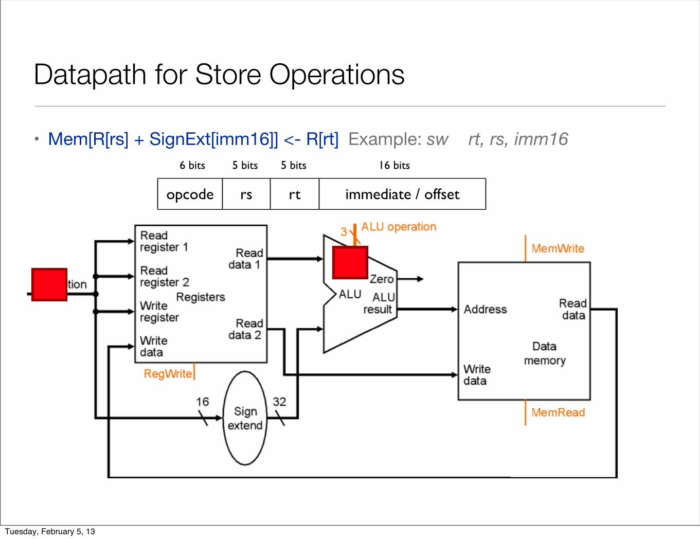
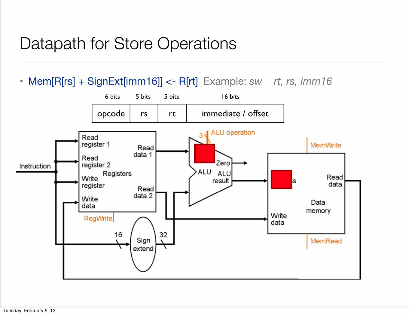
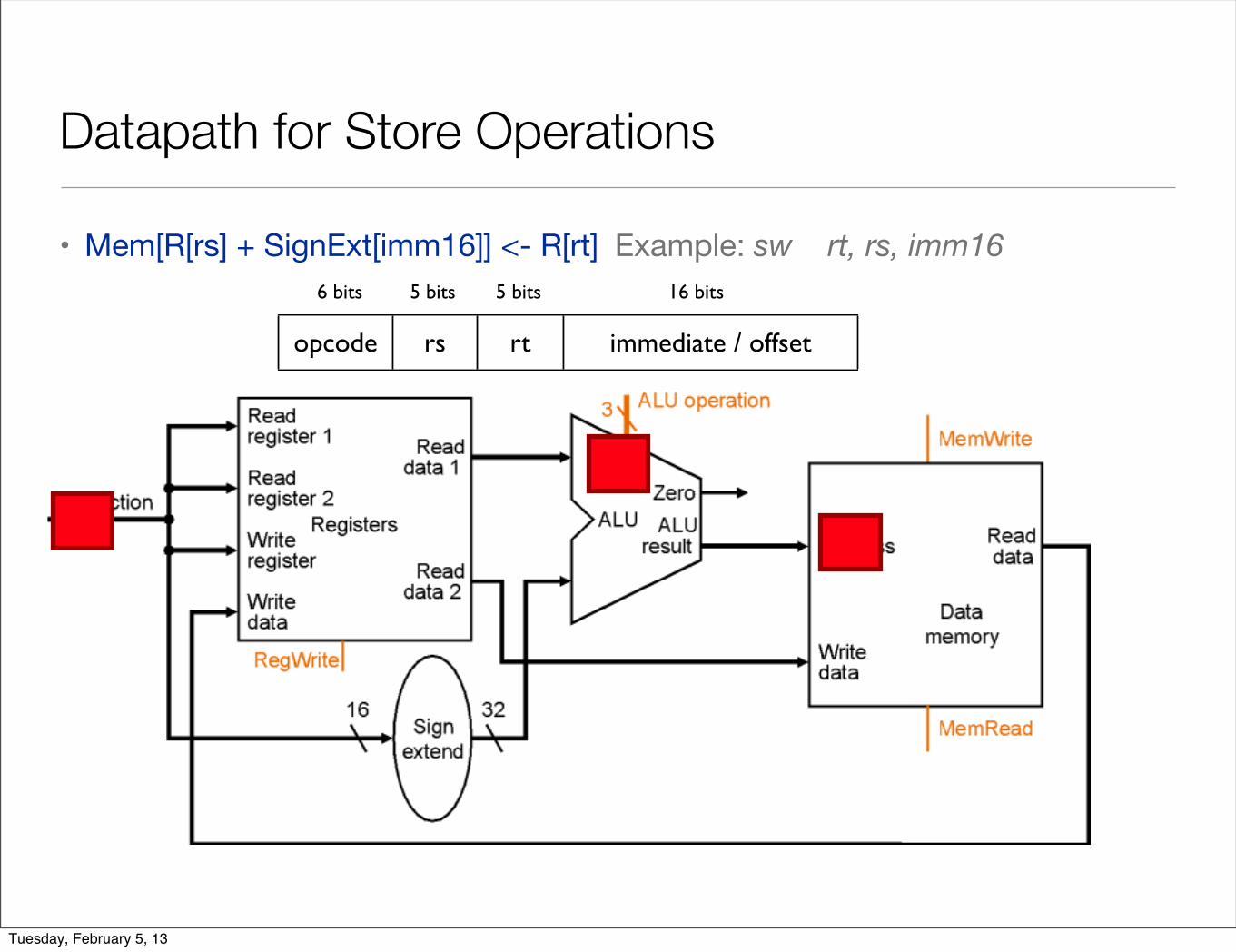
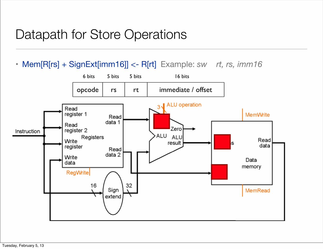
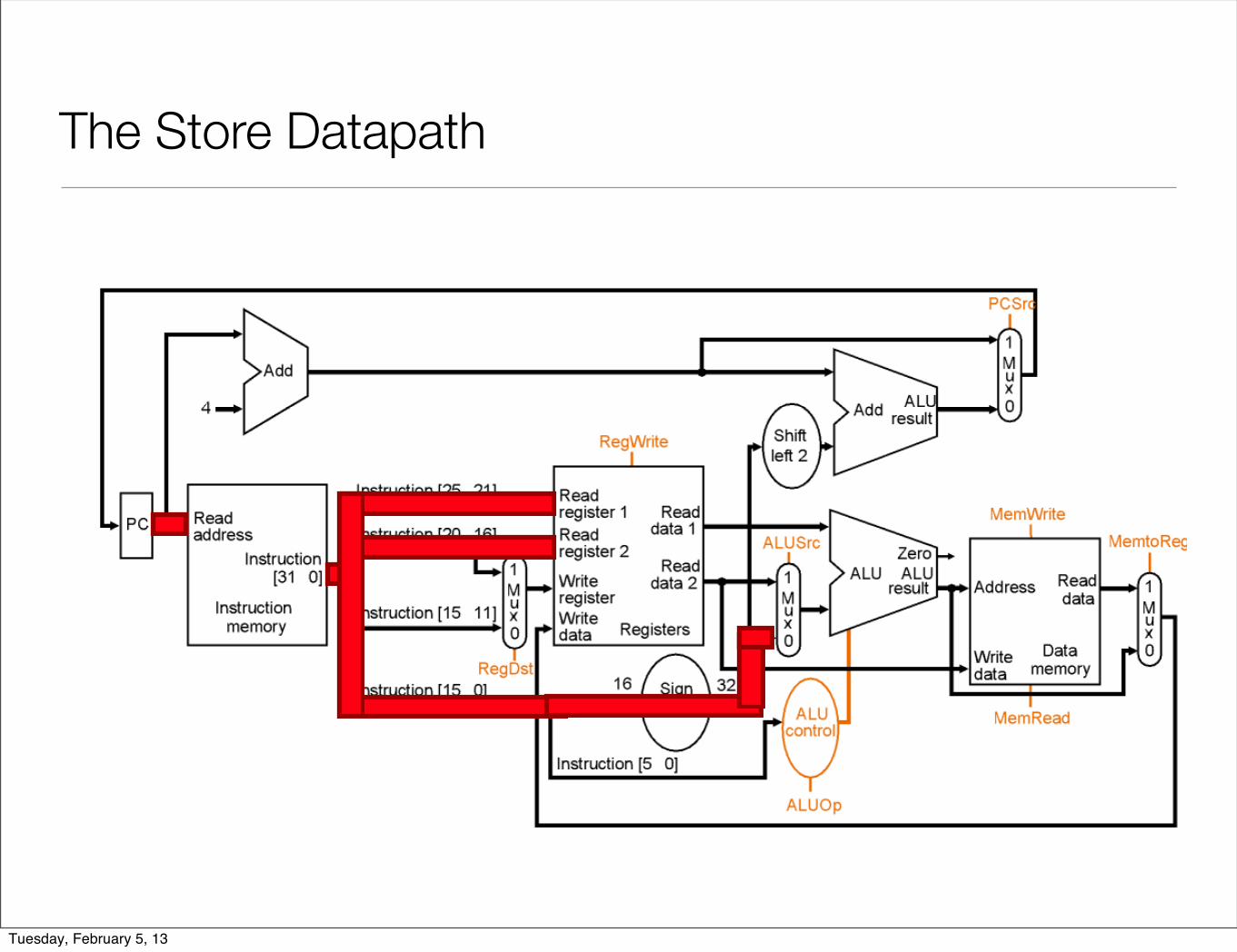
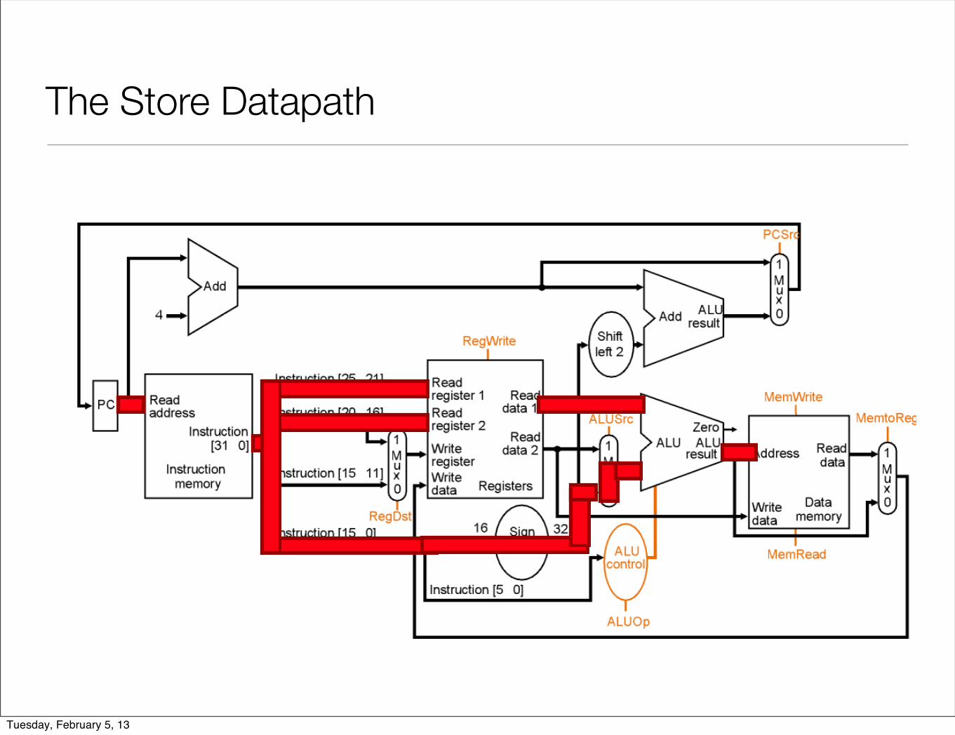
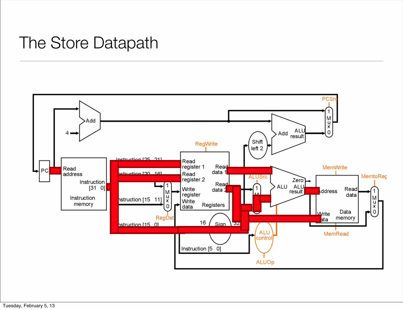
Datapath for Store Operations
• Mem[R[rs] + SignExt[imm16]] <- R[rt] Example: sw rt, rs, imm16
opcode rs rt immediate / offset
6 bits 5 bits 5 bits 16 bits
Tuesday, February 5, 13
Datapath for Store Operations
• Mem[R[rs] + SignExt[imm16]] <- R[rt] Example: sw rt, rs, imm16
opcode rs rt immediate / offset
6 bits 5 bits 5 bits 16 bits
Tuesday, February 5, 13
Datapath for Store Operations
• Mem[R[rs] + SignExt[imm16]] <- R[rt] Example: sw rt, rs, imm16
opcode rs rt immediate / offset
6 bits 5 bits 5 bits 16 bits
Tuesday, February 5, 13
Datapath for Store Operations
• Mem[R[rs] + SignExt[imm16]] <- R[rt] Example: sw rt, rs, imm16
opcode rs rt immediate / offset
6 bits 5 bits 5 bits 16 bits
Tuesday, February 5, 13
Datapath for Store Operations
• Mem[R[rs] + SignExt[imm16]] <- R[rt] Example: sw rt, rs, imm16
opcode rs rt immediate / offset
6 bits 5 bits 5 bits 16 bits
Tuesday, February 5, 13
Datapath for Store Operations
• Mem[R[rs] + SignExt[imm16]] <- R[rt] Example: sw rt, rs, imm16
opcode rs rt immediate / offset
6 bits 5 bits 5 bits 16 bits
Tuesday, February 5, 13
Datapath for Store Operations
• Mem[R[rs] + SignExt[imm16]] <- R[rt] Example: sw rt, rs, imm16
opcode rs rt immediate / offset
6 bits 5 bits 5 bits 16 bits
Tuesday, February 5, 13
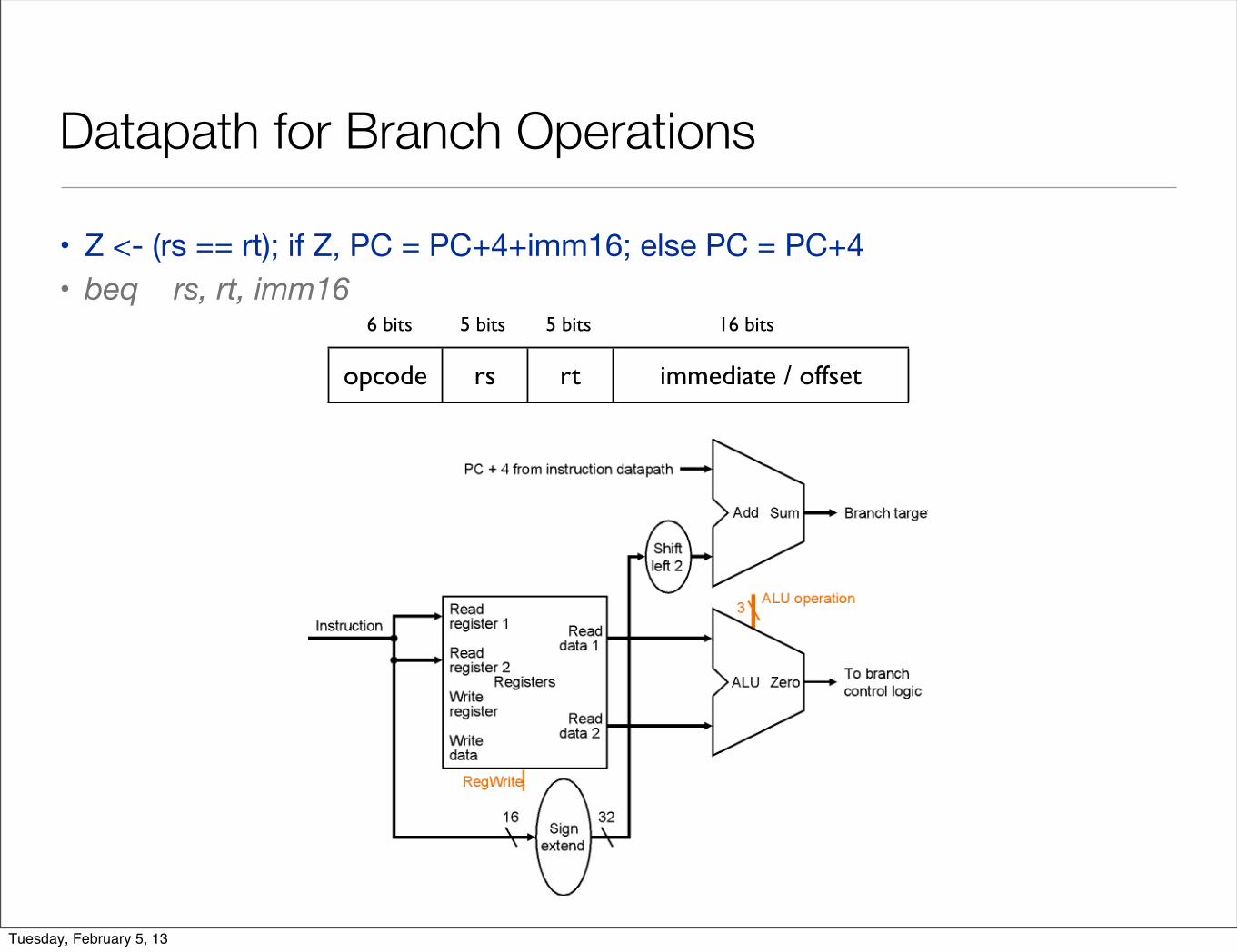
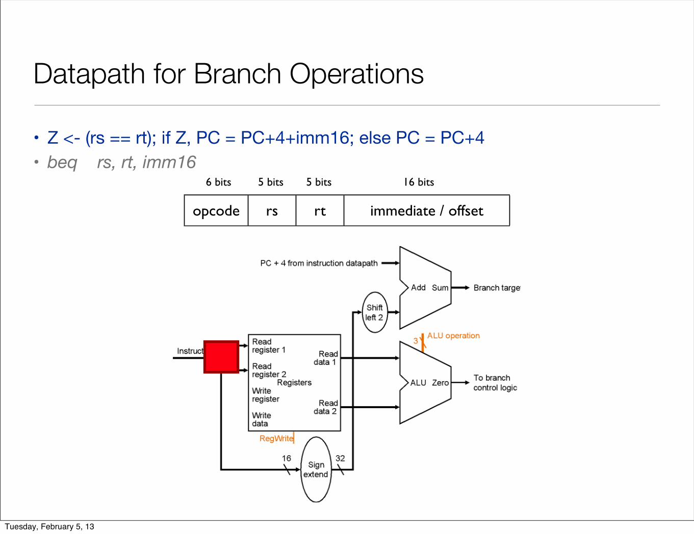
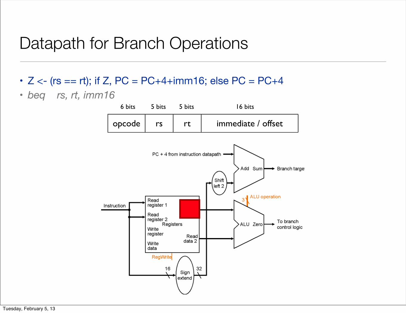
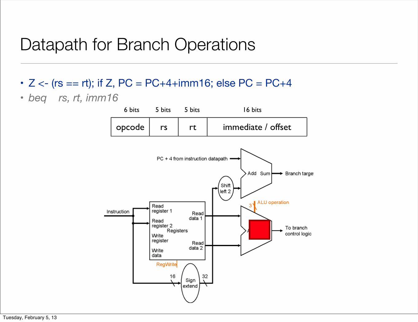
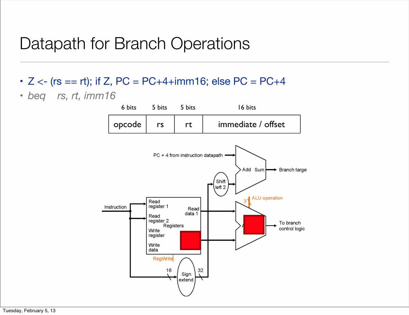
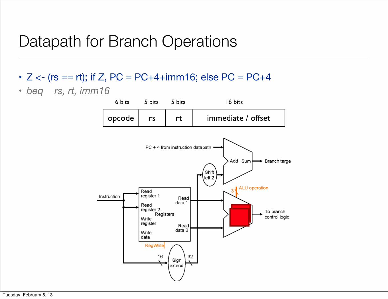
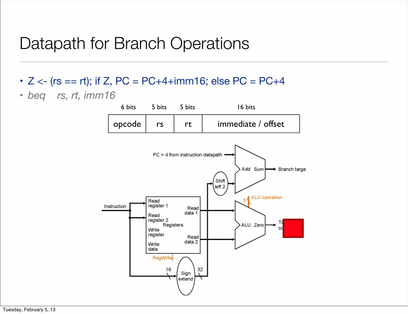
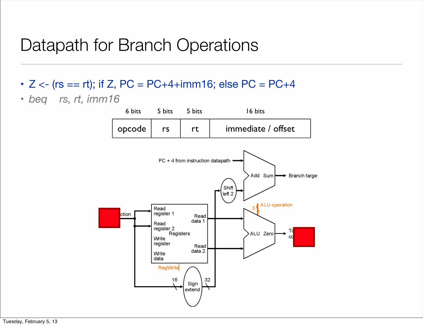
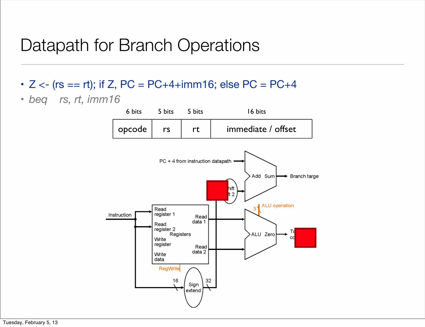
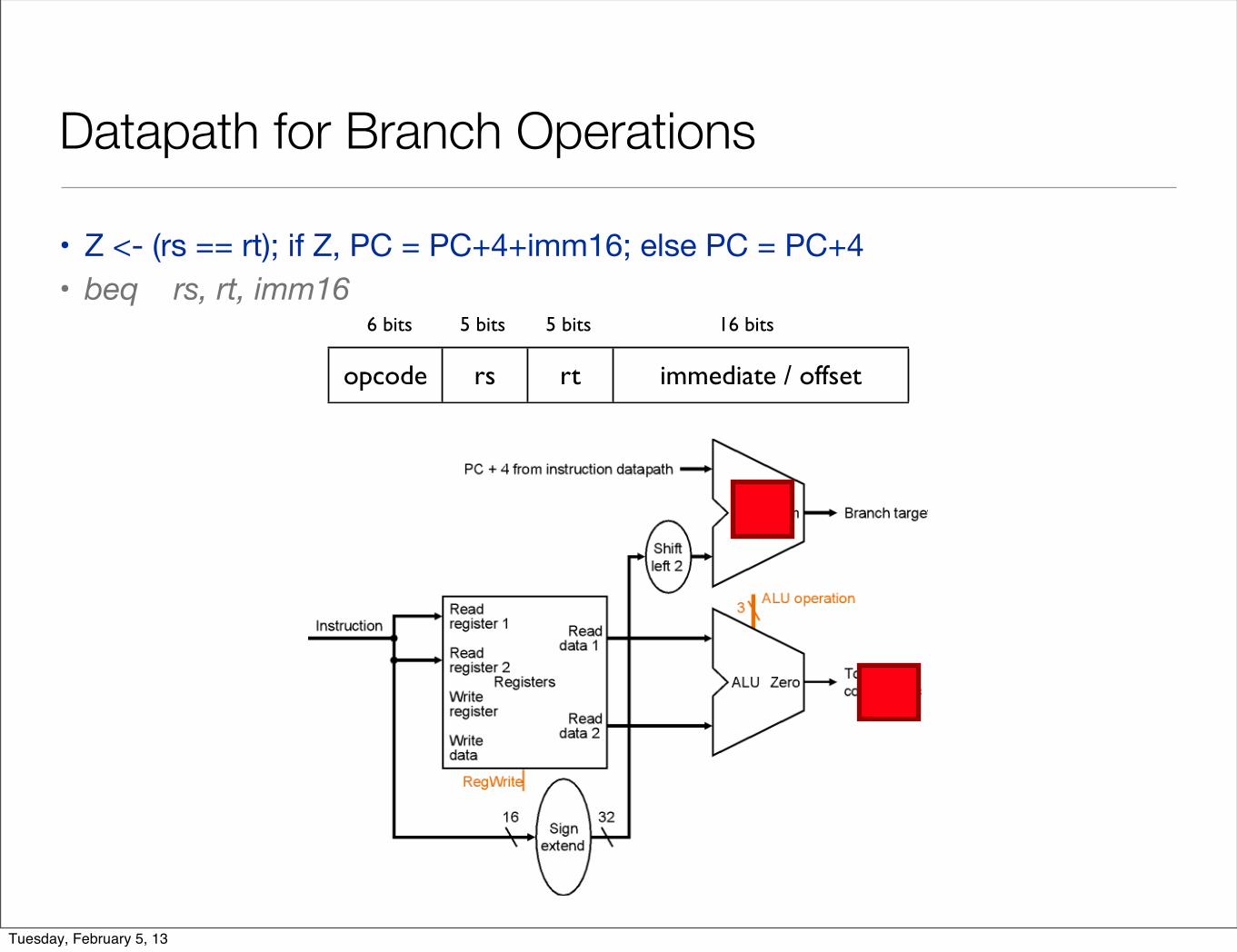
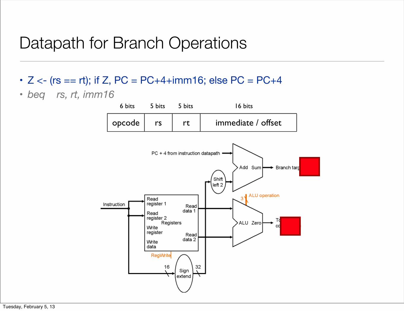
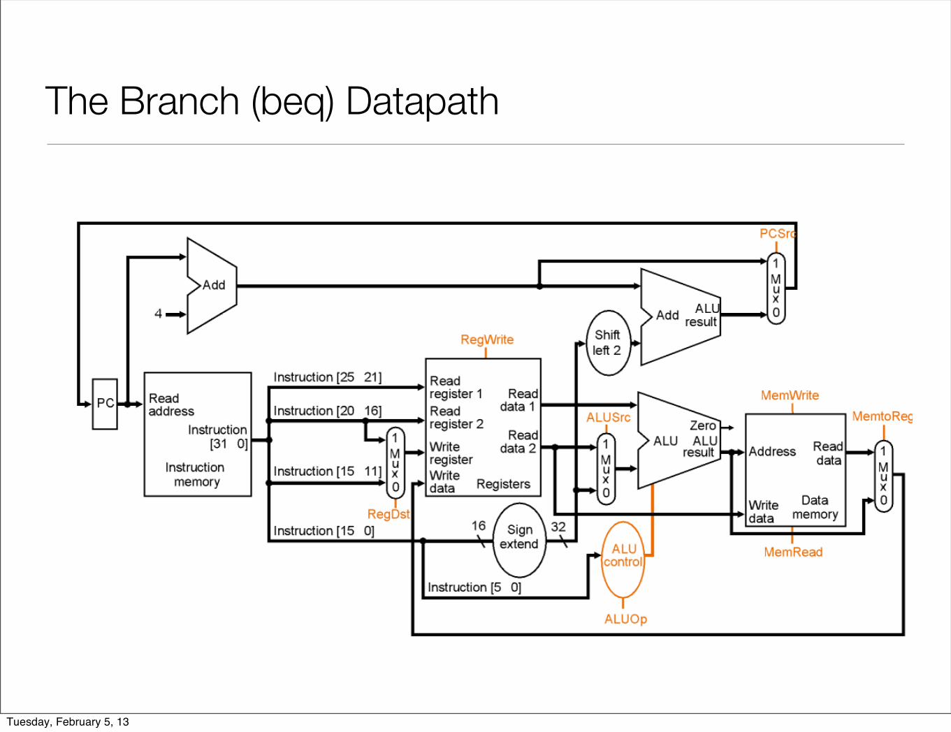
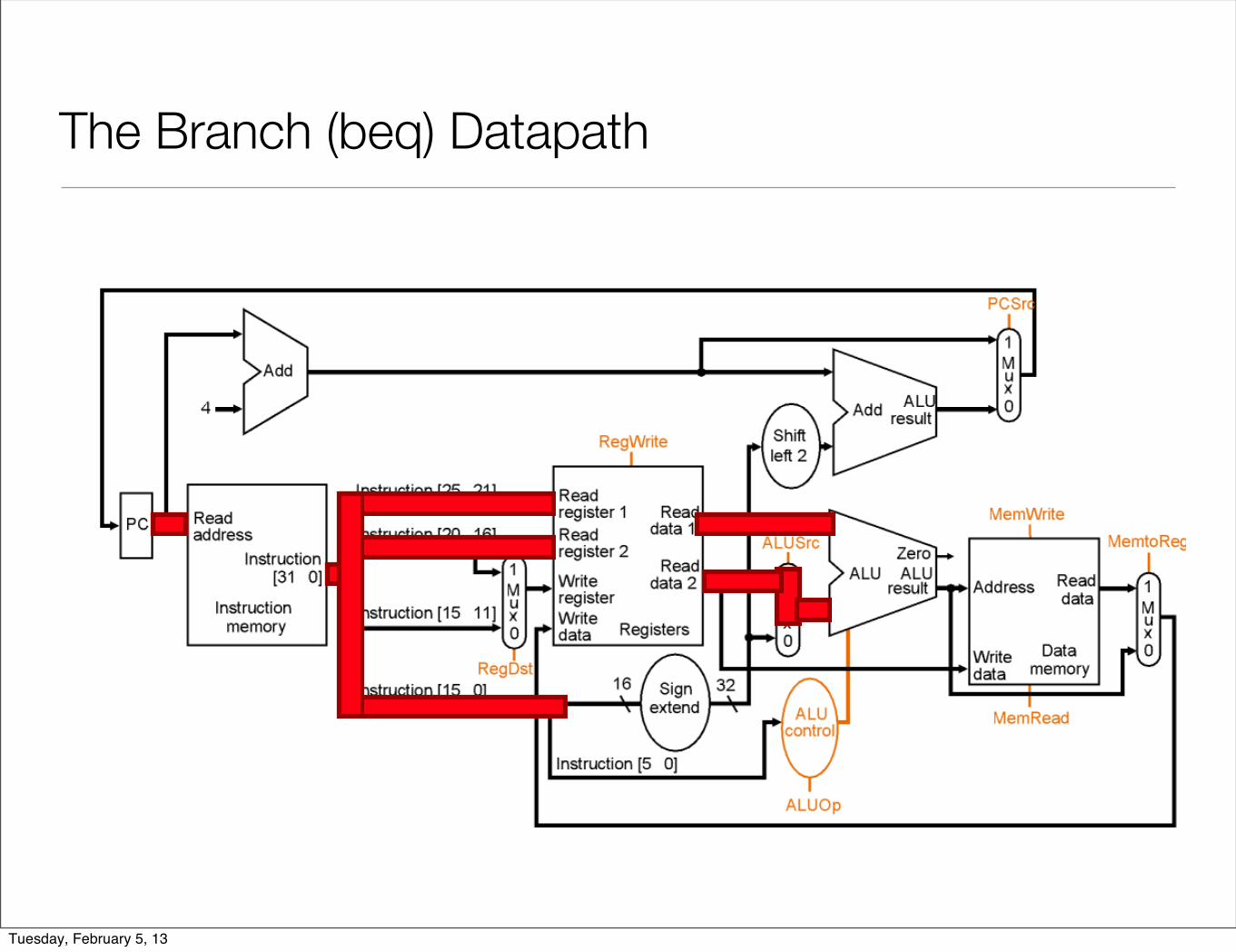
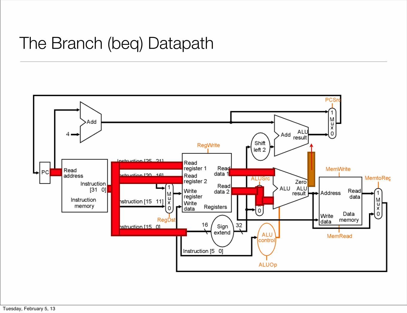
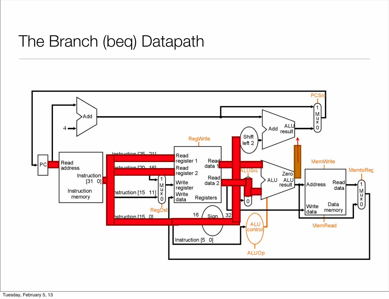
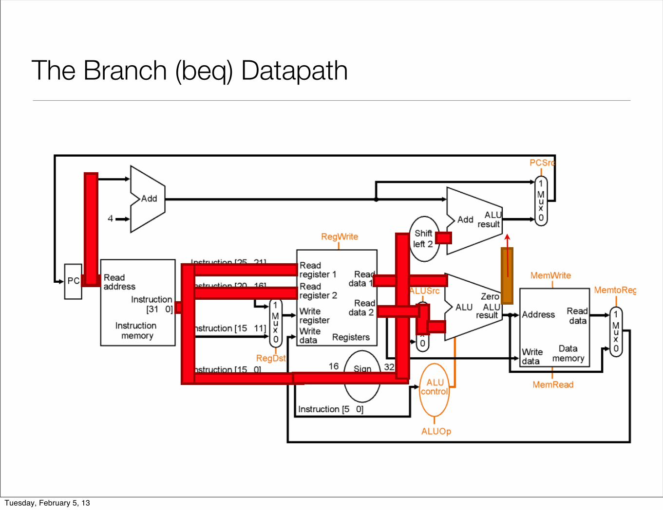
Datapath for Branch Operations
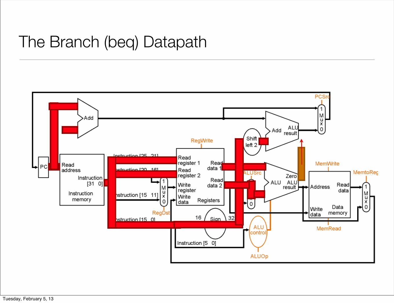
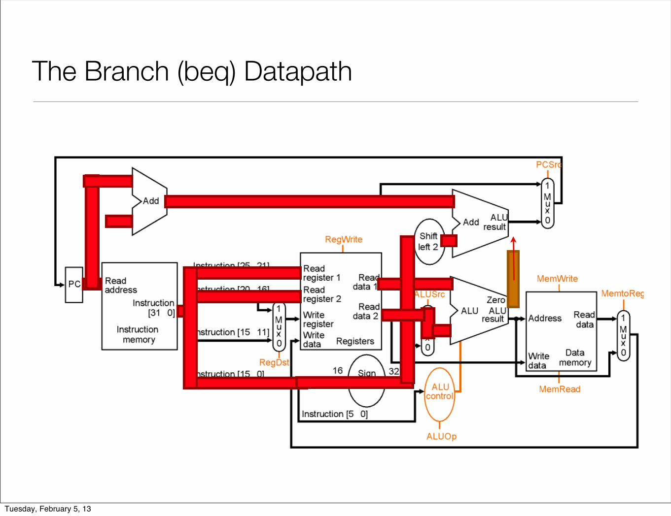
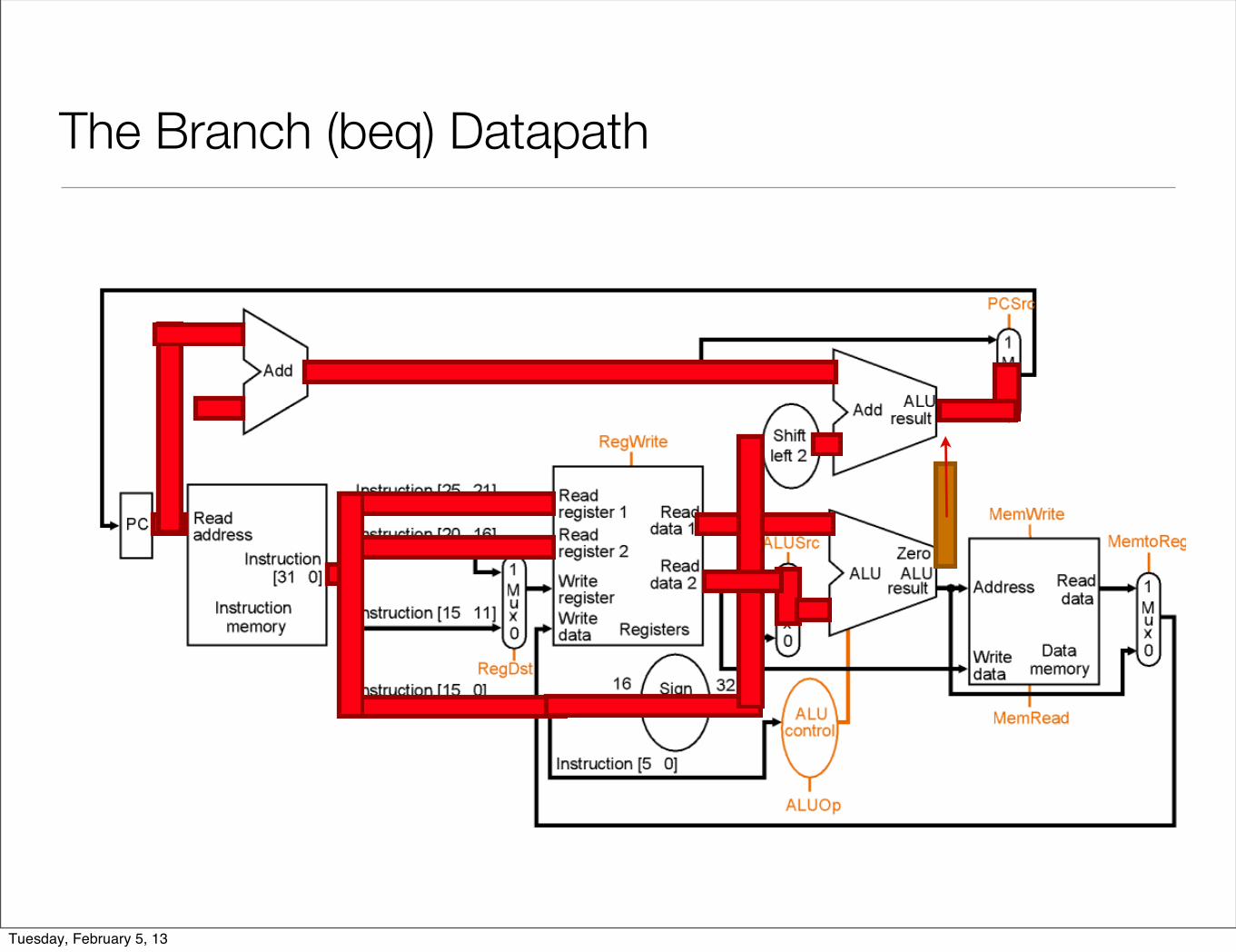
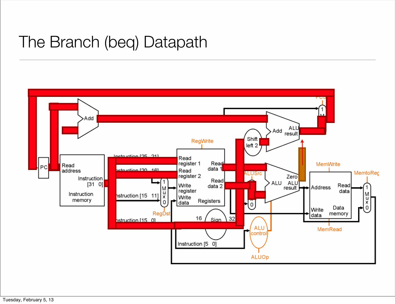
• Z <- (rs == rt); if Z, PC = PC+4+imm16; else PC = PC+4 • beq rs, rt, imm16
opcode rs rt immediate / offset
6 bits 5 bits 5 bits 16 bits
Tuesday, February 5, 13

Datapath for Branch Operations
• Z <- (rs == rt); if Z, PC = PC+4+imm16; else PC = PC+4 • beq rs, rt, imm16
opcode rs rt immediate / offset
6 bits 5 bits 5 bits 16 bits
Tuesday, February 5, 13
Datapath for Branch Operations
• Z <- (rs == rt); if Z, PC = PC+4+imm16; else PC = PC+4 • beq rs, rt, imm16
opcode rs rt immediate / offset
6 bits 5 bits 5 bits 16 bits
Tuesday, February 5, 13
Datapath for Branch Operations
• Z <- (rs == rt); if Z, PC = PC+4+imm16; else PC = PC+4 • beq rs, rt, imm16
opcode rs rt immediate / offset
6 bits 5 bits 5 bits 16 bits
Tuesday, February 5, 13
Datapath for Branch Operations
• Z <- (rs == rt); if Z, PC = PC+4+imm16; else PC = PC+4 • beq rs, rt, imm16
opcode rs rt immediate / offset
6 bits 5 bits 5 bits 16 bits
Tuesday, February 5, 13
Datapath for Branch Operations
• Z <- (rs == rt); if Z, PC = PC+4+imm16; else PC = PC+4 • beq rs, rt, imm16
opcode rs rt immediate / offset
6 bits 5 bits 5 bits 16 bits
Tuesday, February 5, 13
Datapath for Branch Operations
• Z <- (rs == rt); if Z, PC = PC+4+imm16; else PC = PC+4 • beq rs, rt, imm16
opcode rs rt immediate / offset
6 bits 5 bits 5 bits 16 bits
Tuesday, February 5, 13
Datapath for Branch Operations
• Z <- (rs == rt); if Z, PC = PC+4+imm16; else PC = PC+4 • beq rs, rt, imm16
opcode rs rt immediate / offset
6 bits 5 bits 5 bits 16 bits
Tuesday, February 5, 13
Datapath for Branch Operations
• Z <- (rs == rt); if Z, PC = PC+4+imm16; else PC = PC+4 • beq rs, rt, imm16
opcode rs rt immediate / offset
6 bits 5 bits 5 bits 16 bits
Tuesday, February 5, 13

Datapath for Branch Operations
• Z <- (rs == rt); if Z, PC = PC+4+imm16; else PC = PC+4 • beq rs, rt, imm16
opcode rs rt immediate / offset
6 bits 5 bits 5 bits 16 bits
Tuesday, February 5, 13
Datapath for Branch Operations
• Z <- (rs == rt); if Z, PC = PC+4+imm16; else PC = PC+4 • beq rs, rt, imm16
opcode rs rt immediate / offset
6 bits 5 bits 5 bits 16 bits
Tuesday, February 5, 13
Datapath for Branch Operations
• Z <- (rs == rt); if Z, PC = PC+4+imm16; else PC = PC+4 • beq rs, rt, imm16
opcode rs rt immediate / offset
6 bits 5 bits 5 bits 16 bits
Tuesday, February 5, 13
Datapath for Branch Operations
• Z <- (rs == rt); if Z, PC = PC+4+imm16; else PC = PC+4 • beq rs, rt, imm16
opcode rs rt immediate / offset
6 bits 5 bits 5 bits 16 bits
Tuesday, February 5, 13
Control Logic??288 Chapter 5 The Processor: Datapath and Control
While easier to understand, this approach is not practical, since it would beslower than an implementation that allows different instruction classes to take dif-ferent numbers of clock cycles, each of which could be much shorter. After design-ing the control for this simple machine, we will look at an implementation thatuses multiple clock cycles for each instruction. This multicycle design is used
FIGURE 5.2 The basic implementation of the MIPS subset including the necessary multiplexors and controllines. The top multiplexor controls what value replaces the PC (PC + 4 or the branch destination address); the multiplexor is con-trolled by the gate that “ands” together the Zero output of the ALU and a control signal that indicates that the instruction is abranch. The multiplexor whose output returns to the register file is used to steer the output of the ALU (in the case of an arithmetic-logical instruction) or the output of the data memory (in the case of a load) for writing into the register file. Finally, the bottommostmultiplexor is used to determine whether the second ALU input is from the registers (for a nonimmediate arithmetic-logicalinstruction) or from the offset field of the instruction (for an immediate operation, a load or store, or a branch). The added controllines are straightforward and determine the operation performed at the ALU, whether the data memory should read or write, andwhether the registers should perform a write operation. The control lines are shown in color to make them easier to see.
Data
Register #
Register #
Register #
PC Address Instruction
Instructionmemory
Registers ALU Address
Data
Datamemory
AddAdd
4
MemWrite
MemRead
Mux
Mux
Mux
Control
RegWrite
Zero
Branch
ALU operation
Tuesday, February 5, 13
Binary Arithmetic for the Next Address
Tuesday, February 5, 13
Binary Arithmetic for the Next Address
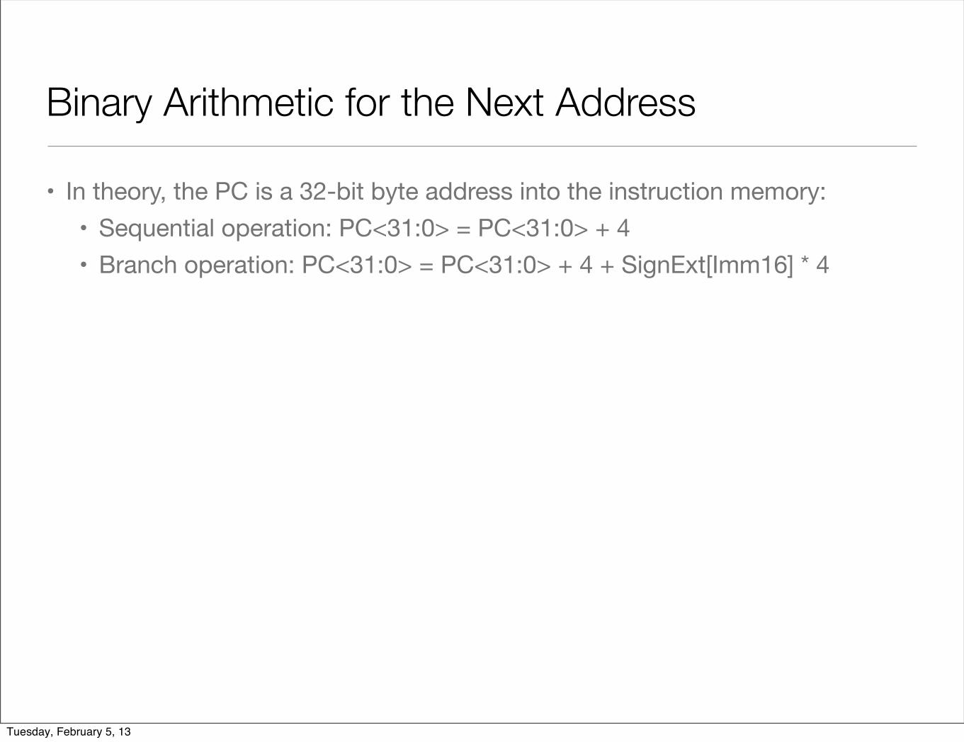
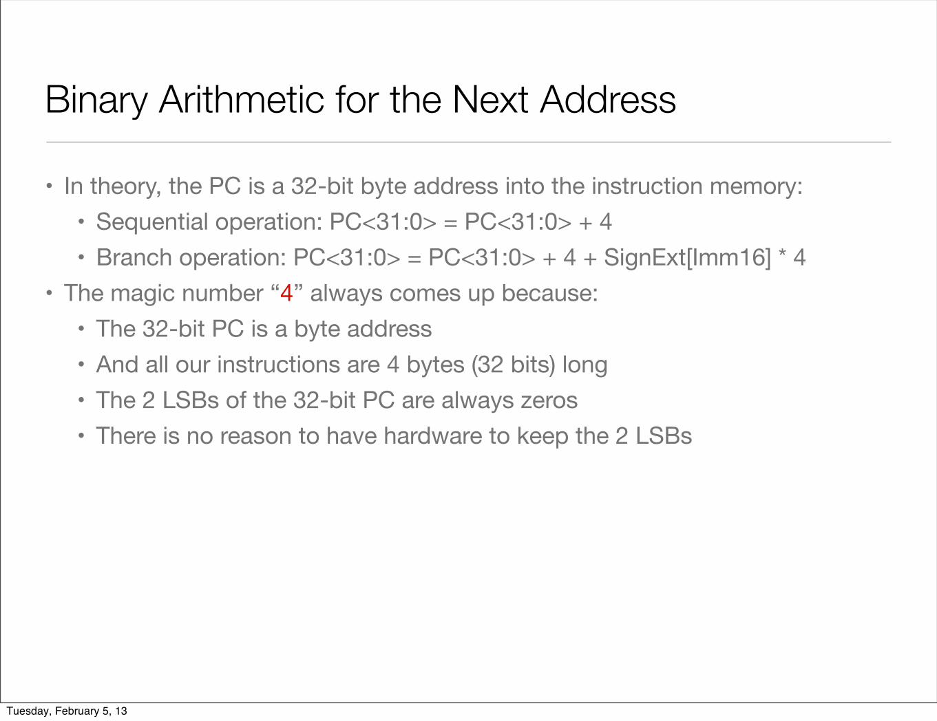
• In theory, the PC is a 32-bit byte address into the instruction memory:• Sequential operation: PC<31:0> = PC<31:0> + 4• Branch operation: PC<31:0> = PC<31:0> + 4 + SignExt[Imm16] * 4
Tuesday, February 5, 13
Binary Arithmetic for the Next Address
• In theory, the PC is a 32-bit byte address into the instruction memory:• Sequential operation: PC<31:0> = PC<31:0> + 4• Branch operation: PC<31:0> = PC<31:0> + 4 + SignExt[Imm16] * 4
• The magic number “4” always comes up because:• The 32-bit PC is a byte address• And all our instructions are 4 bytes (32 bits) long• The 2 LSBs of the 32-bit PC are always zeros• There is no reason to have hardware to keep the 2 LSBs
Tuesday, February 5, 13

Binary Arithmetic for the Next Address
• In theory, the PC is a 32-bit byte address into the instruction memory:• Sequential operation: PC<31:0> = PC<31:0> + 4• Branch operation: PC<31:0> = PC<31:0> + 4 + SignExt[Imm16] * 4
• The magic number “4” always comes up because:• The 32-bit PC is a byte address• And all our instructions are 4 bytes (32 bits) long• The 2 LSBs of the 32-bit PC are always zeros• There is no reason to have hardware to keep the 2 LSBs
• In practice, we can simplify the hardware by using a 30-bit PC<31:2>:• Sequential operation: PC<31:2> = PC<31:2> + 1• Branch operation: PC<31:2> = PC<31:2> + 1 + SignExt[Imm16]• In either case: Instruction Memory Address = PC<31:2> concat “00”
Tuesday, February 5, 13
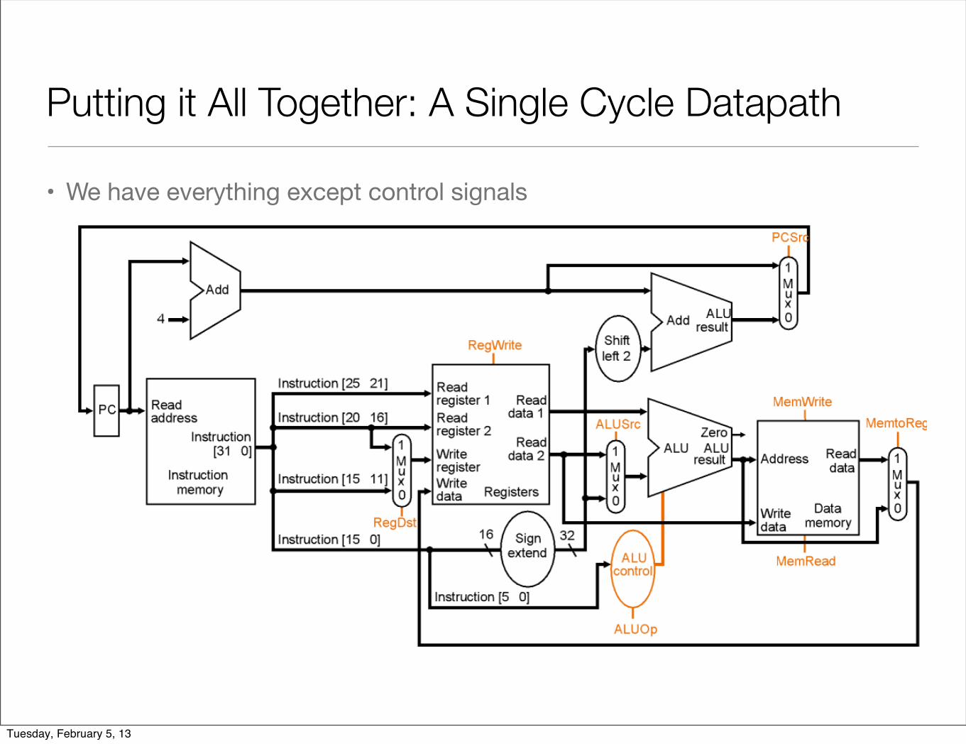
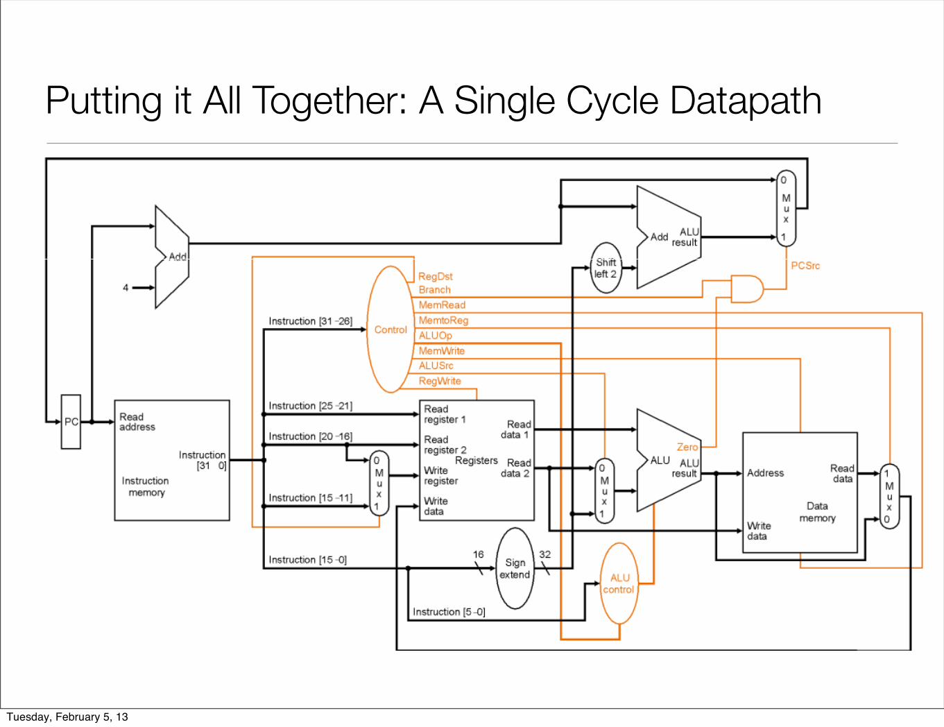
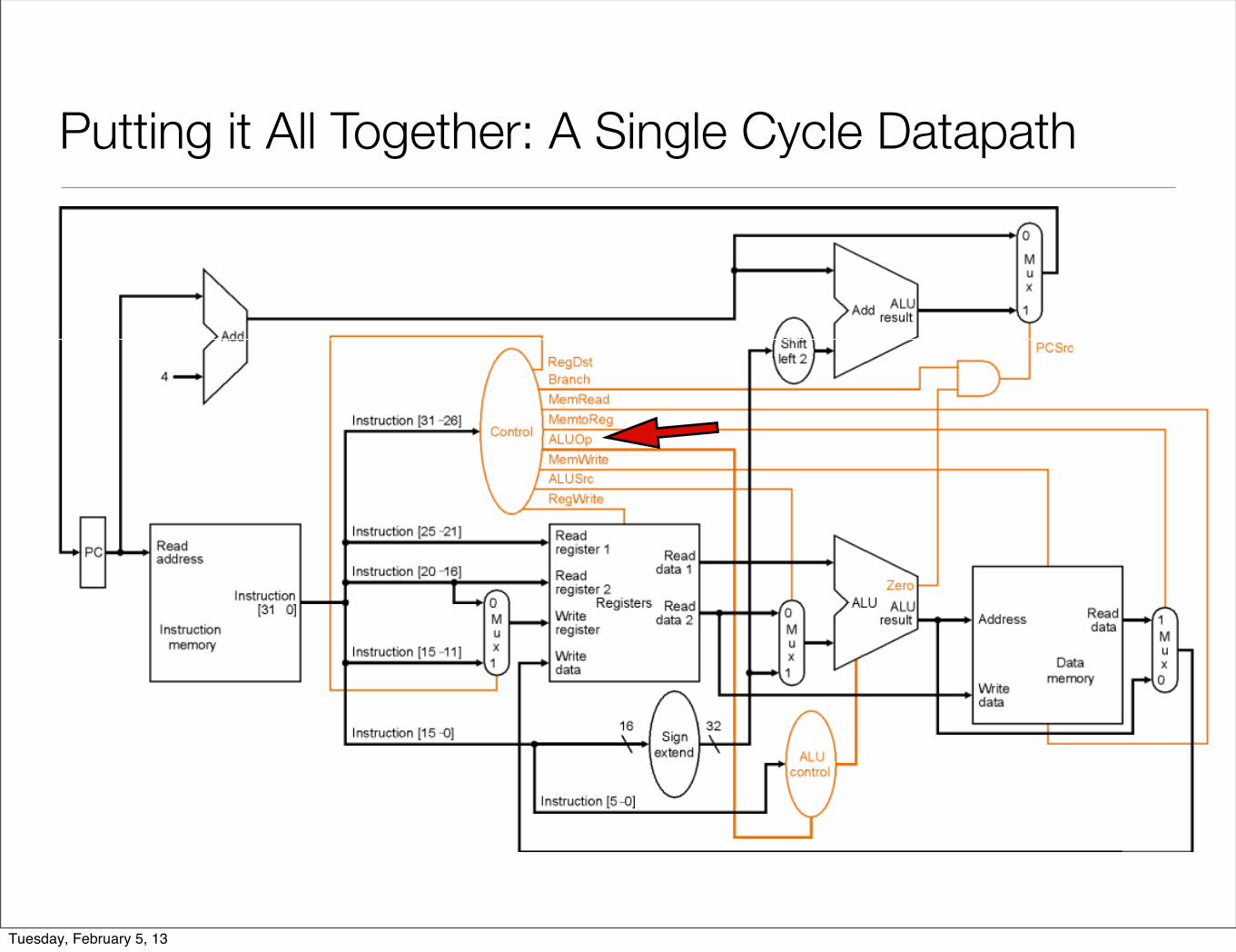
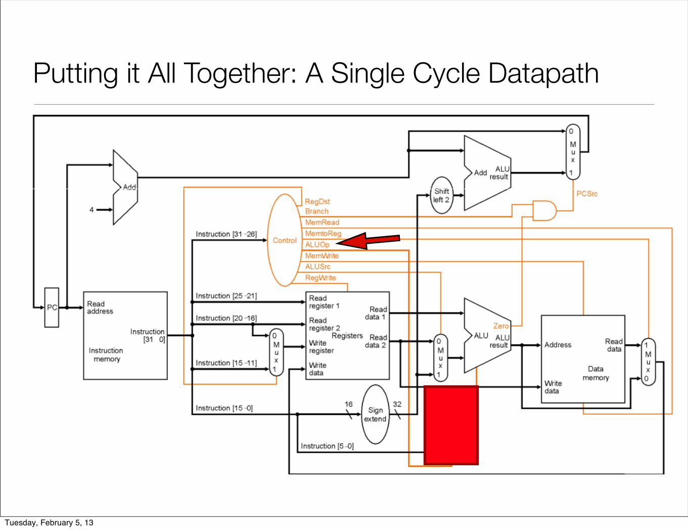
Putting it All Together: A Single Cycle Datapath
• We have everything except control signals
Tuesday, February 5, 13

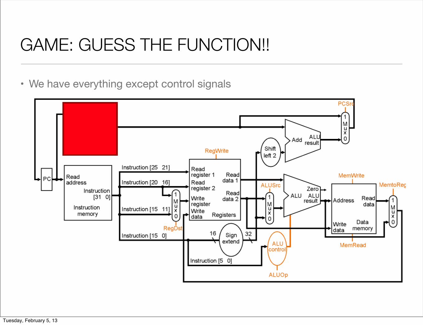
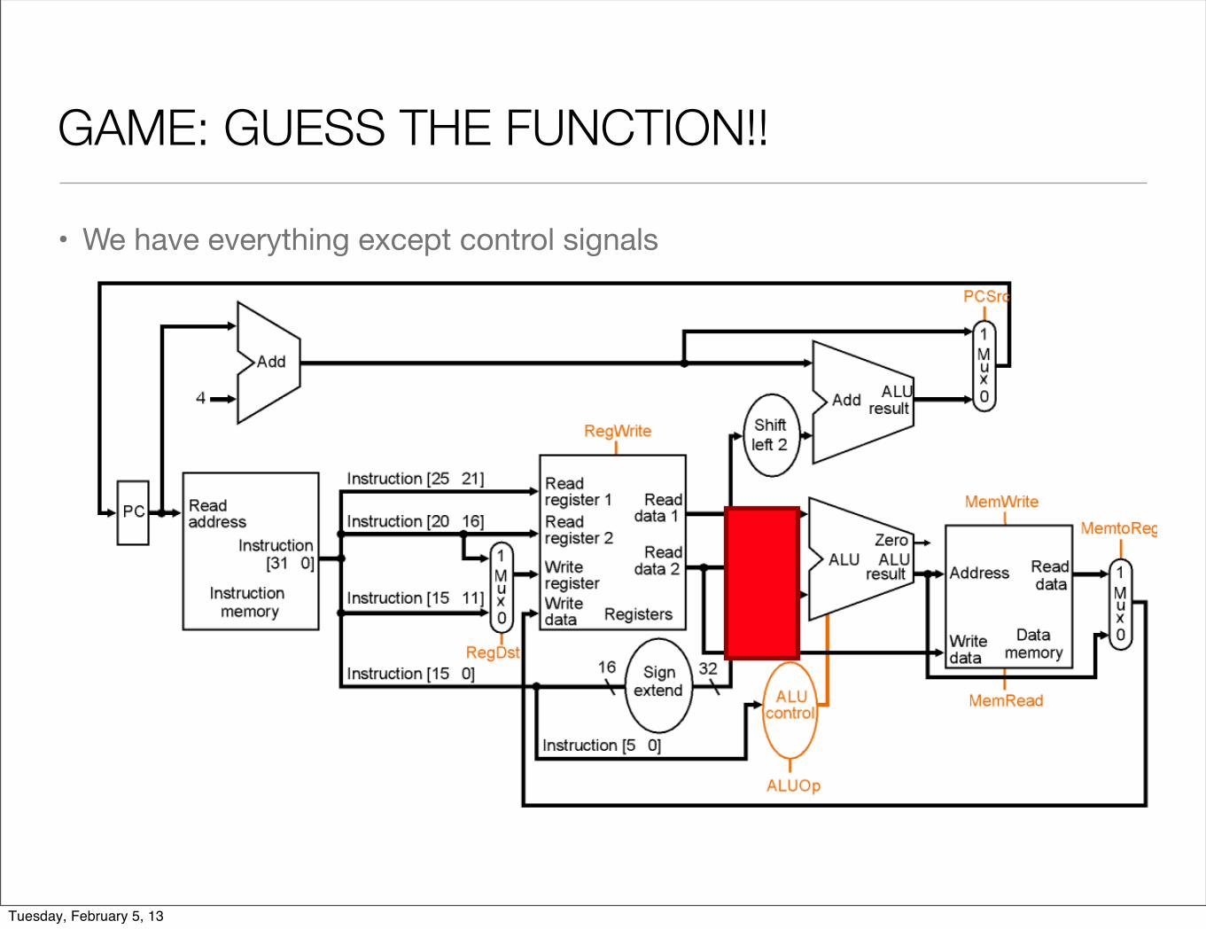
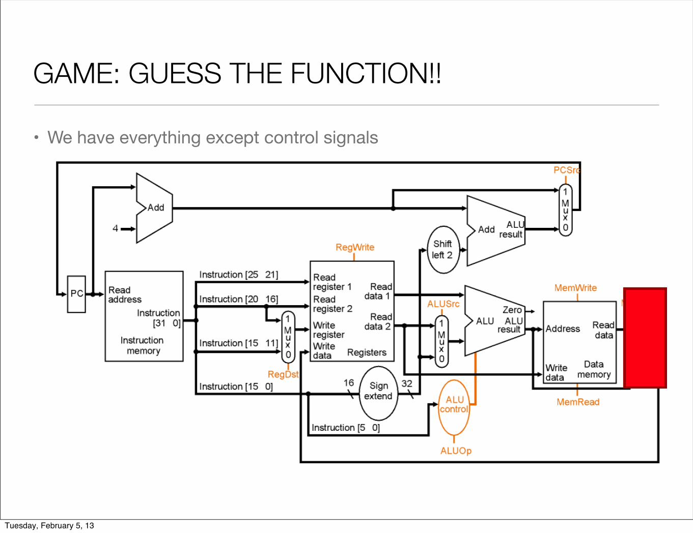
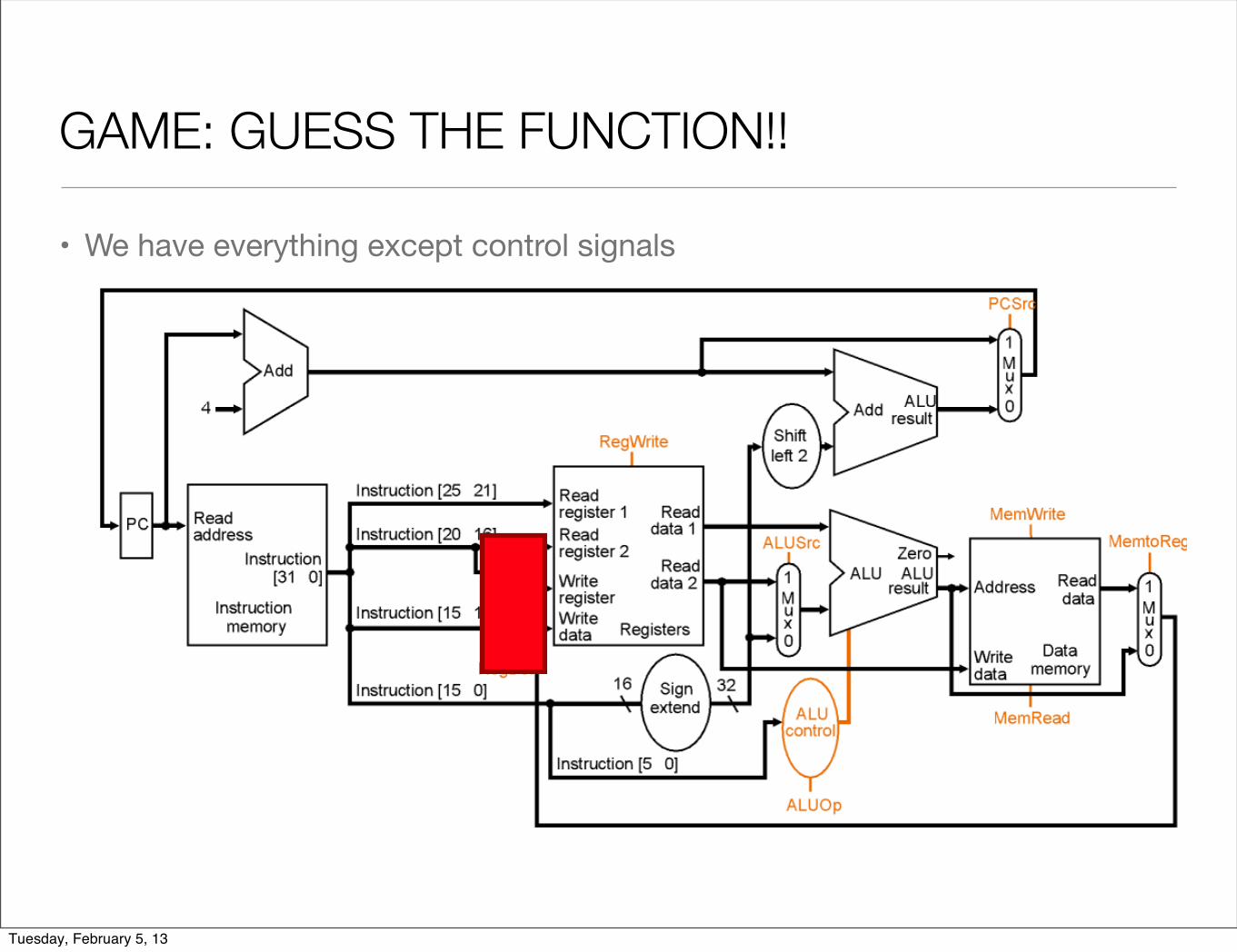
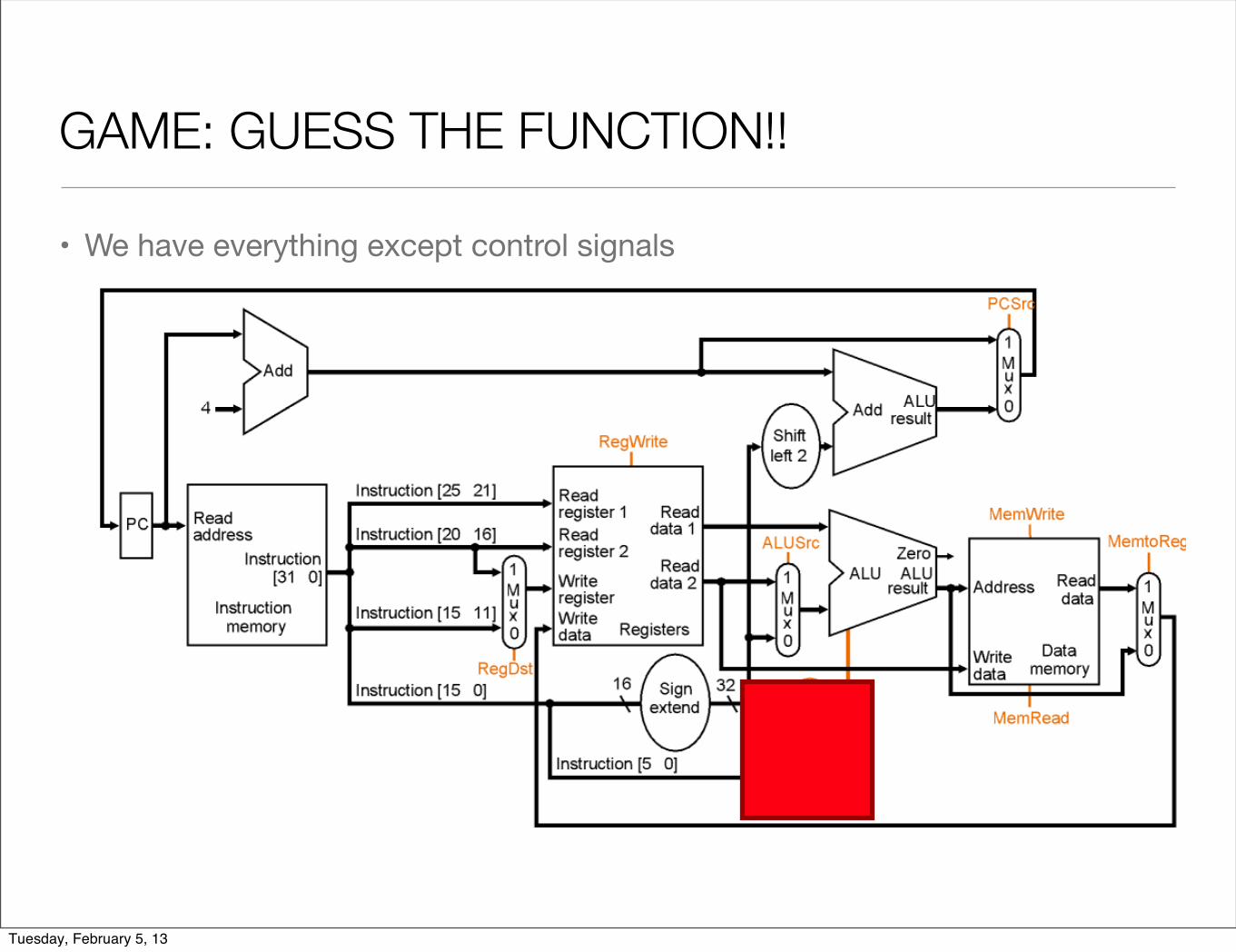
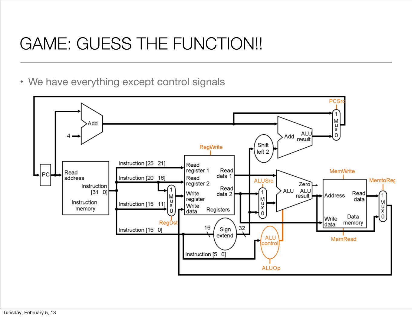
GAME: GUESS THE FUNCTION!!
• We have everything except control signals
Tuesday, February 5, 13
GAME: GUESS THE FUNCTION!!
• We have everything except control signals
Tuesday, February 5, 13
GAME: GUESS THE FUNCTION!!
• We have everything except control signals
Tuesday, February 5, 13
GAME: GUESS THE FUNCTION!!
• We have everything except control signals
Tuesday, February 5, 13
GAME: GUESS THE FUNCTION!!
• We have everything except control signals
Tuesday, February 5, 13

GAME: GUESS THE FUNCTION!!
• We have everything except control signals
Tuesday, February 5, 13
GAME: GUESS THE FUNCTION!!
• We have everything except control signals
Tuesday, February 5, 13
GAME: GUESS THE FUNCTION!!
• We have everything except control signals
Tuesday, February 5, 13
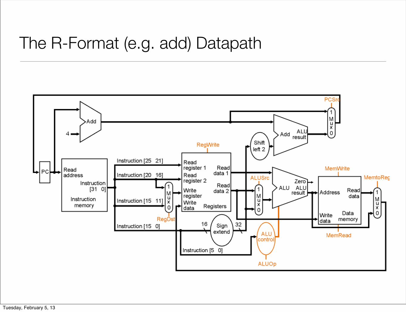
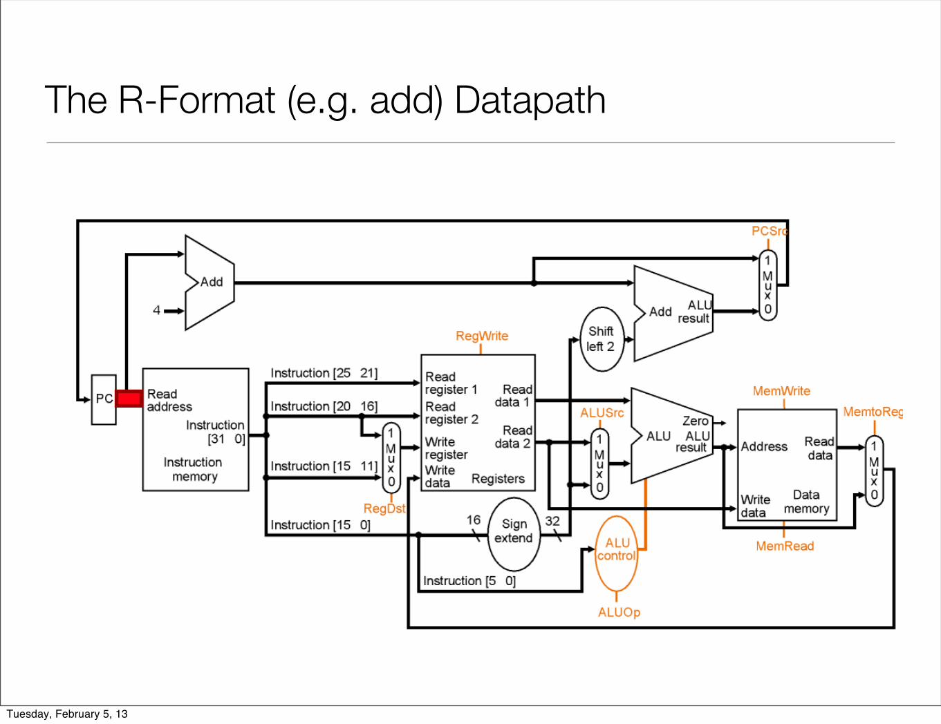
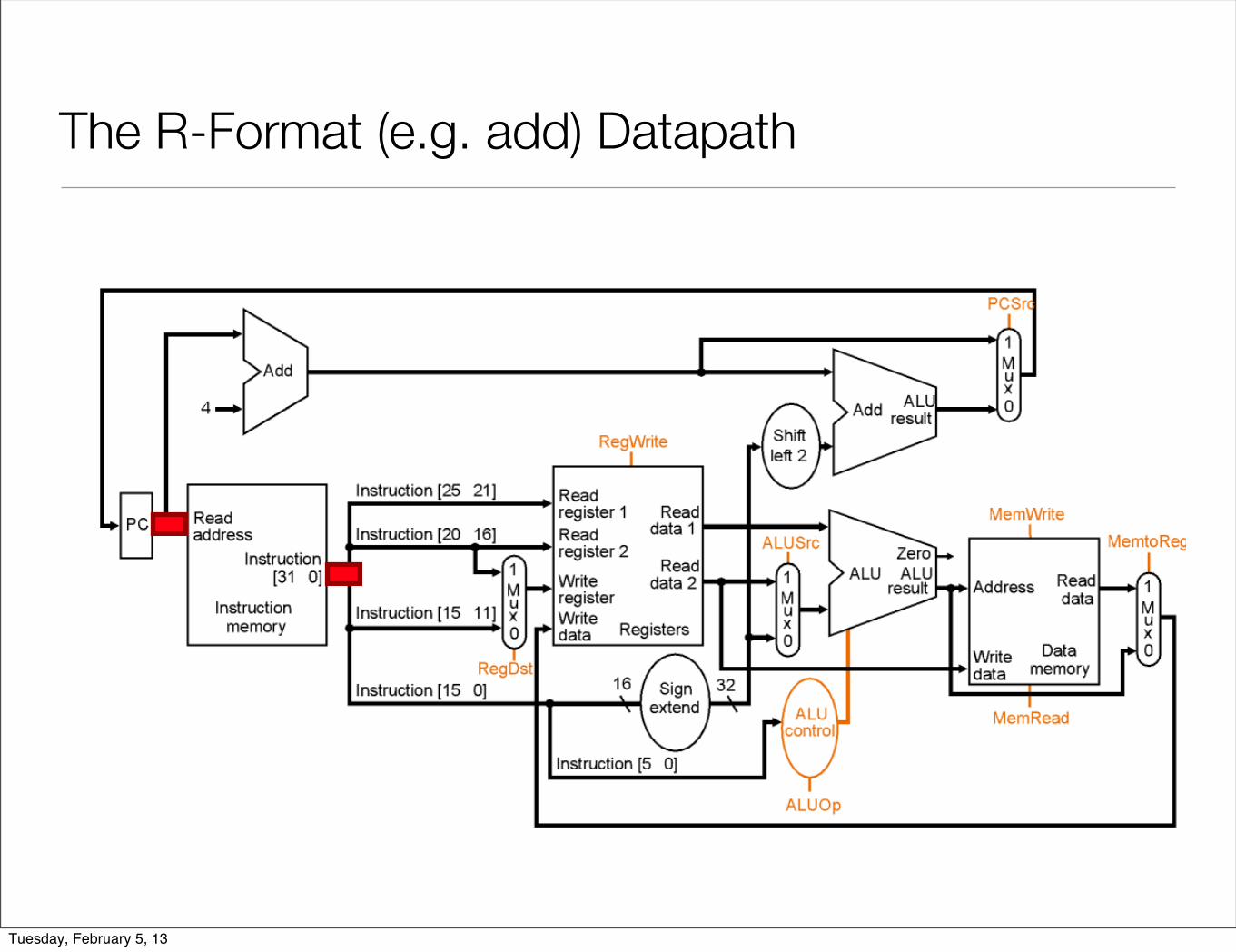
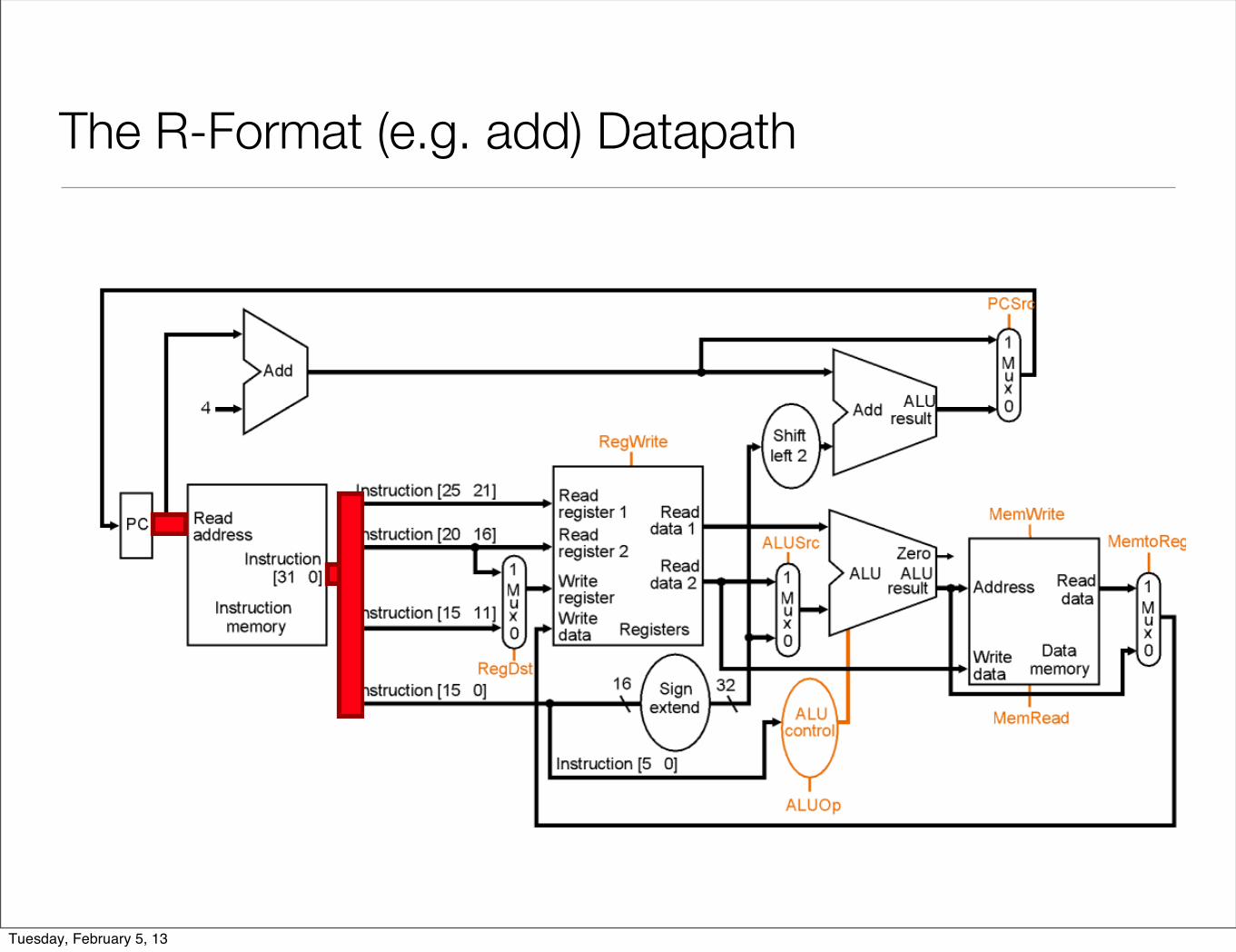
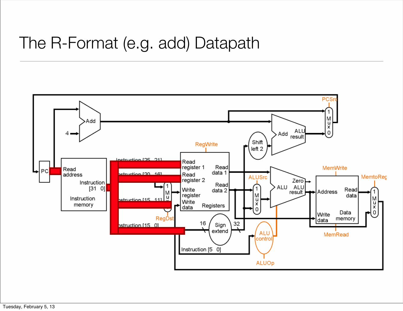
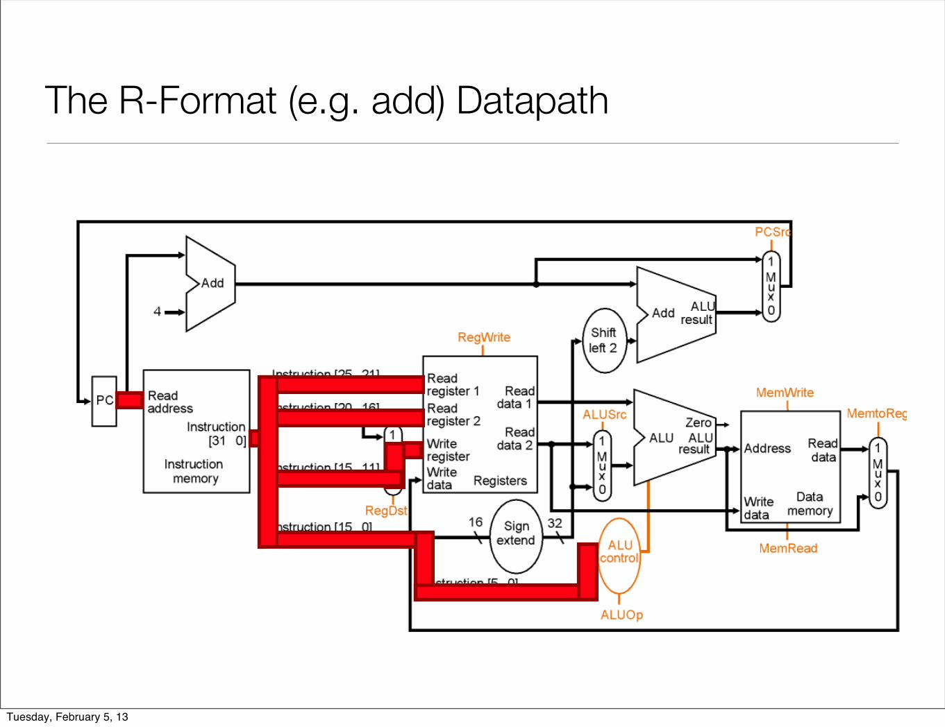
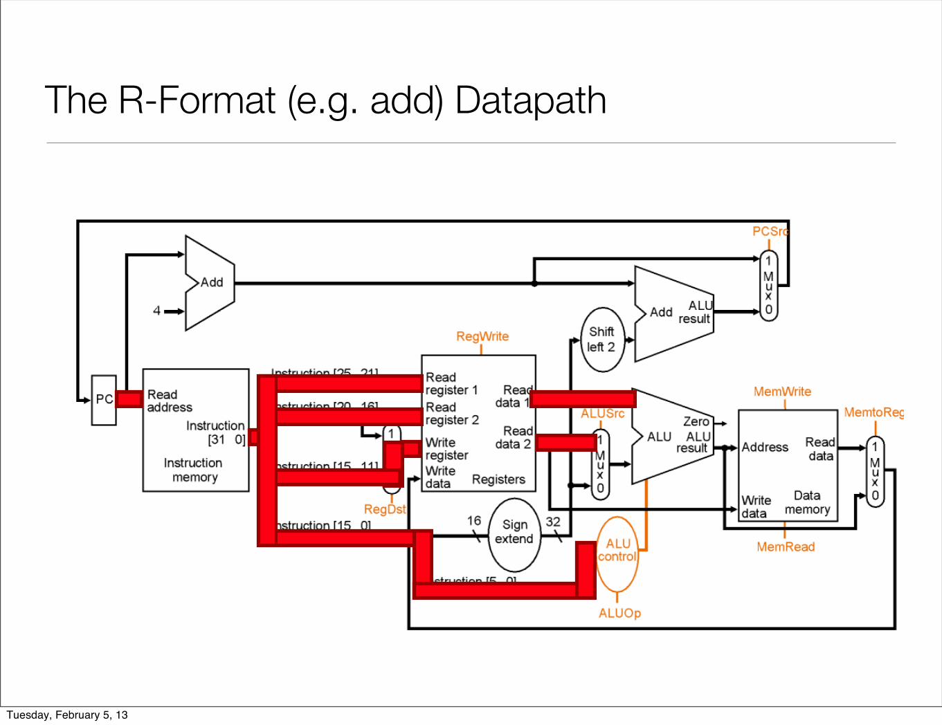
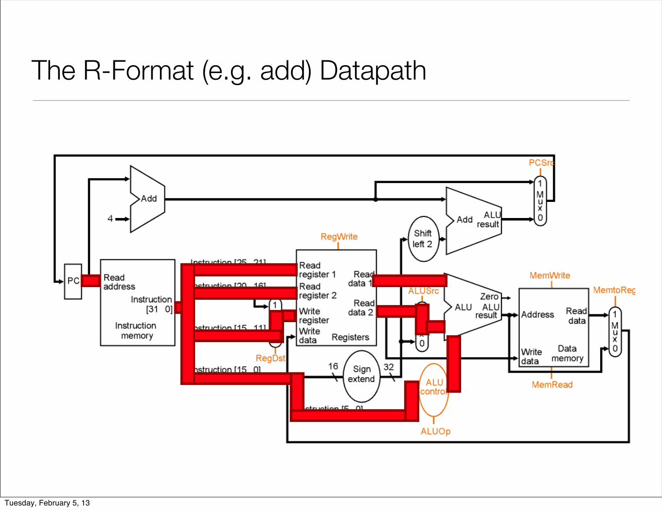
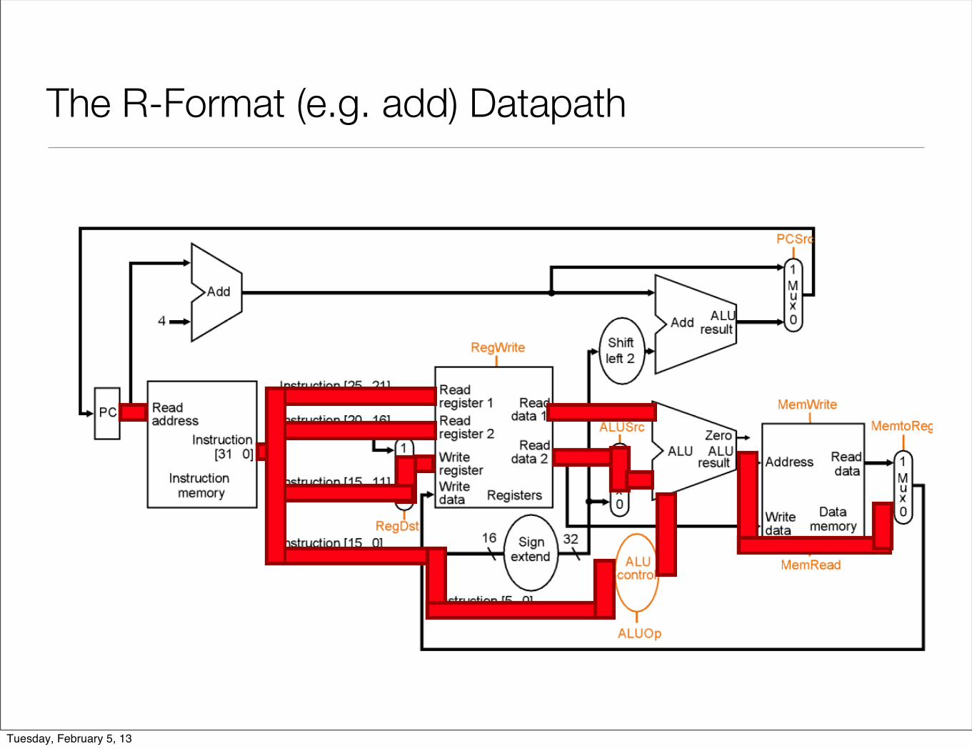
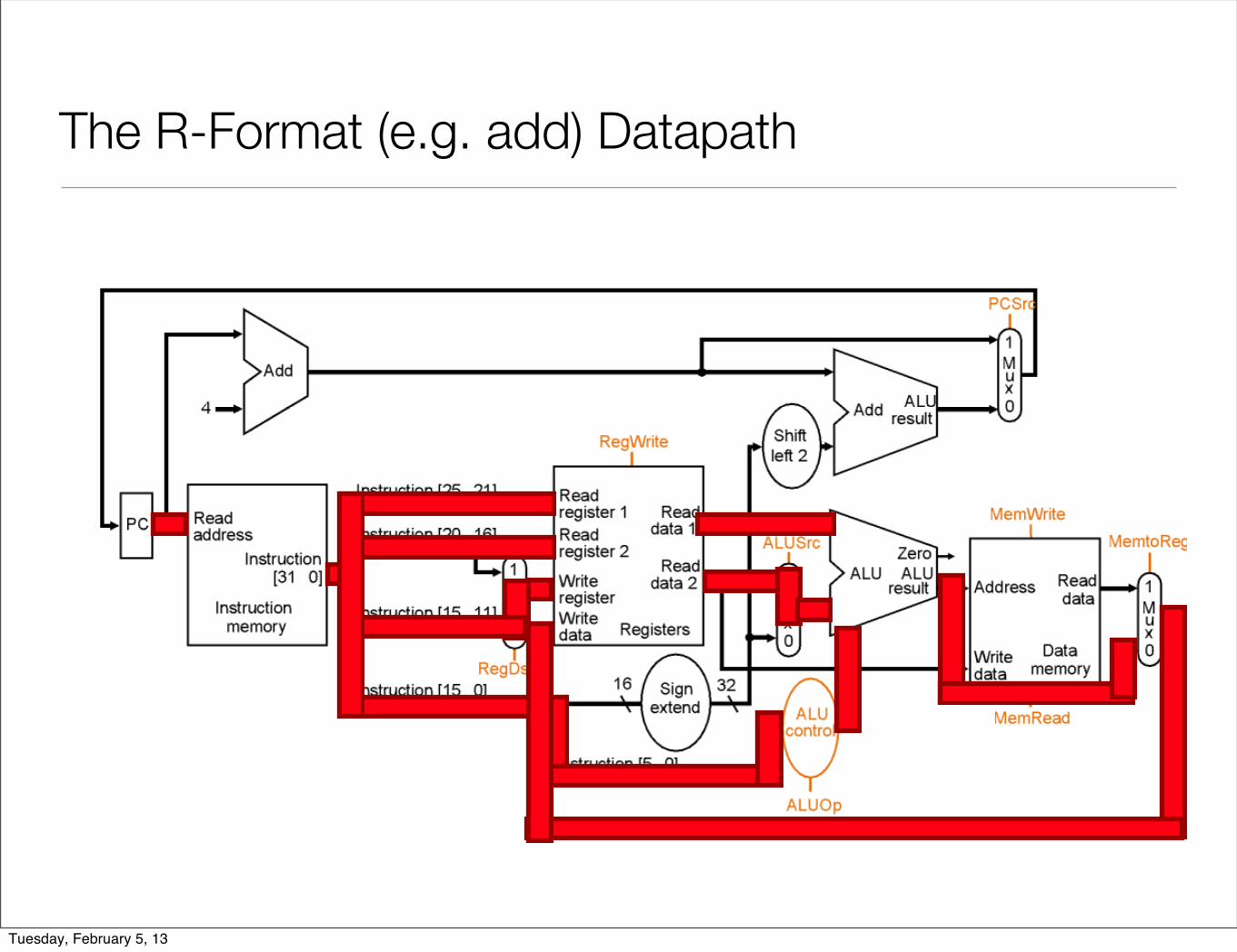
The R-Format (e.g. add) Datapath
Tuesday, February 5, 13
The R-Format (e.g. add) Datapath
Tuesday, February 5, 13
The R-Format (e.g. add) Datapath
Tuesday, February 5, 13
The R-Format (e.g. add) Datapath
Tuesday, February 5, 13
The R-Format (e.g. add) Datapath
Tuesday, February 5, 13

The R-Format (e.g. add) Datapath
Tuesday, February 5, 13
The R-Format (e.g. add) Datapath
Tuesday, February 5, 13
The R-Format (e.g. add) Datapath
Tuesday, February 5, 13

The R-Format (e.g. add) Datapath
Tuesday, February 5, 13
The R-Format (e.g. add) Datapath
Tuesday, February 5, 13
The R-Format (e.g. add) Datapath
Tuesday, February 5, 13
The R-Format (e.g. add) Datapath
Tuesday, February 5, 13

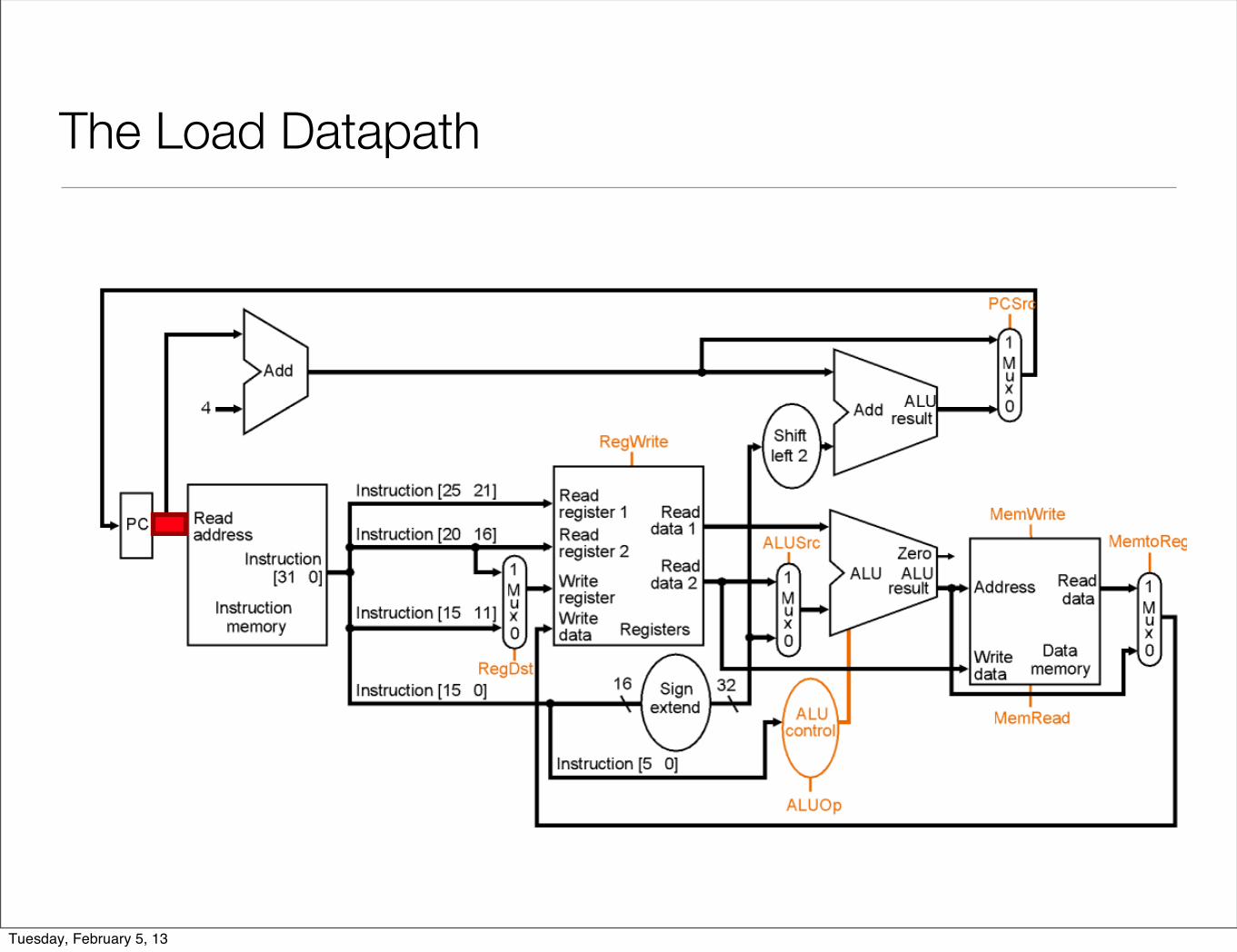
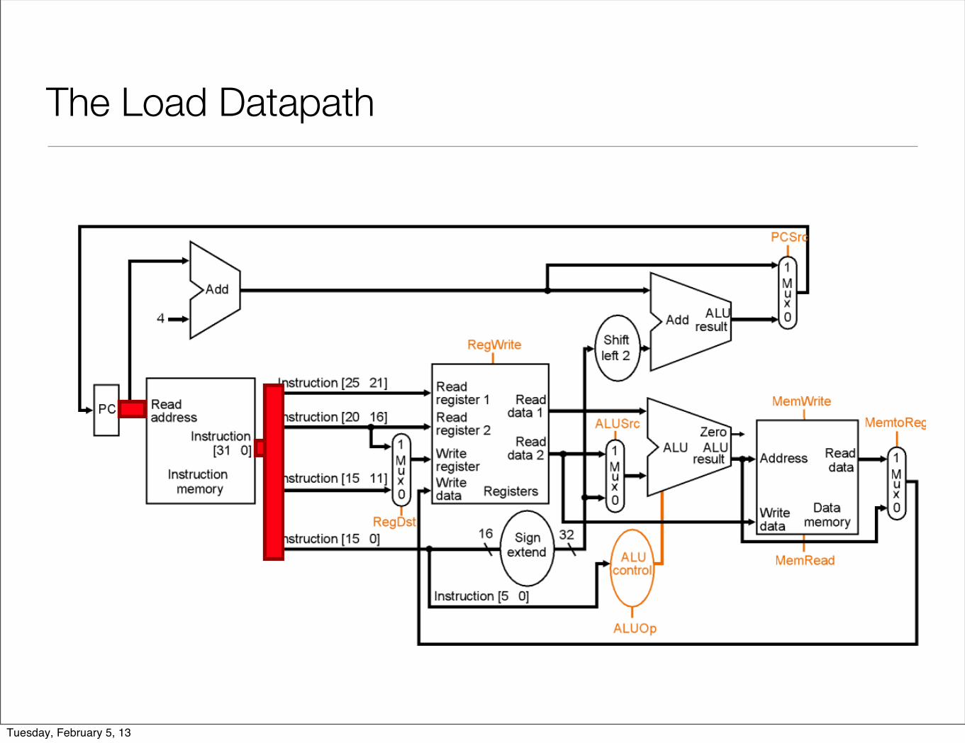
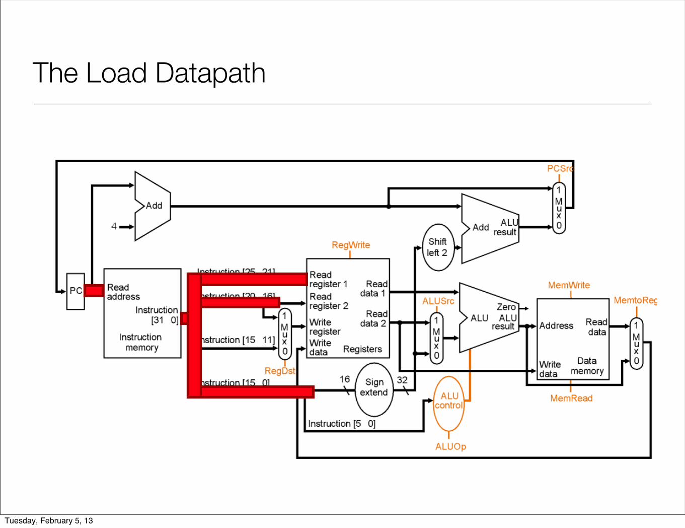
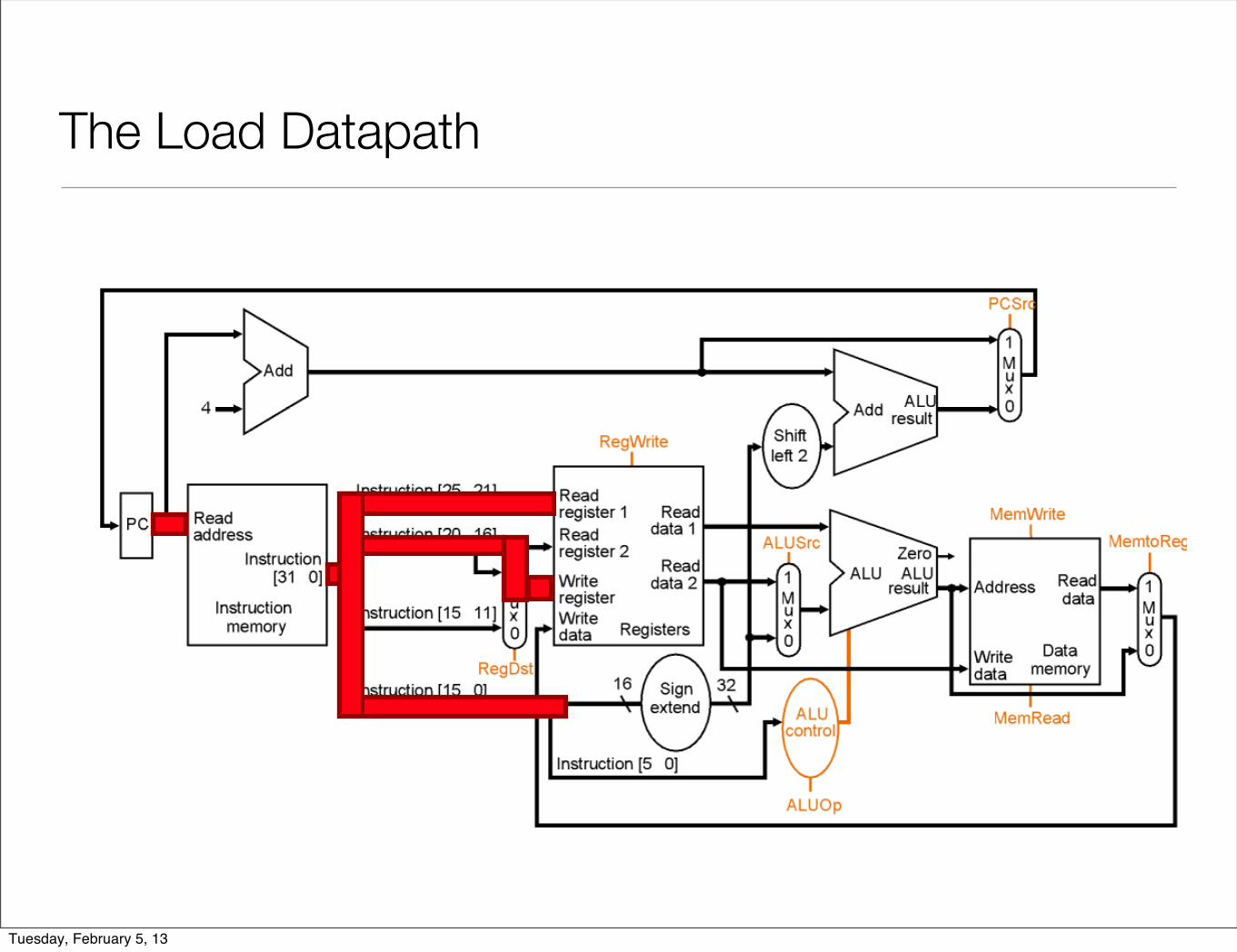
The Load Datapath
Tuesday, February 5, 13
The Load Datapath
Tuesday, February 5, 13
The Load Datapath
Tuesday, February 5, 13
The Load Datapath
Tuesday, February 5, 13
The Load Datapath
Tuesday, February 5, 13
The Load Datapath
Tuesday, February 5, 13
The Load Datapath
Tuesday, February 5, 13

The Load Datapath
Tuesday, February 5, 13
The Load Datapath
Tuesday, February 5, 13
The Load Datapath
Tuesday, February 5, 13
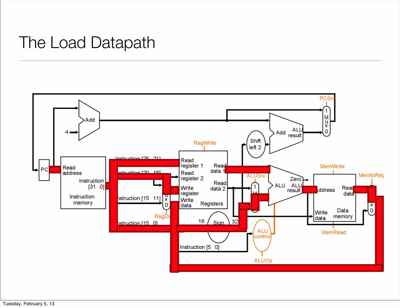
The Load Datapath
Tuesday, February 5, 13
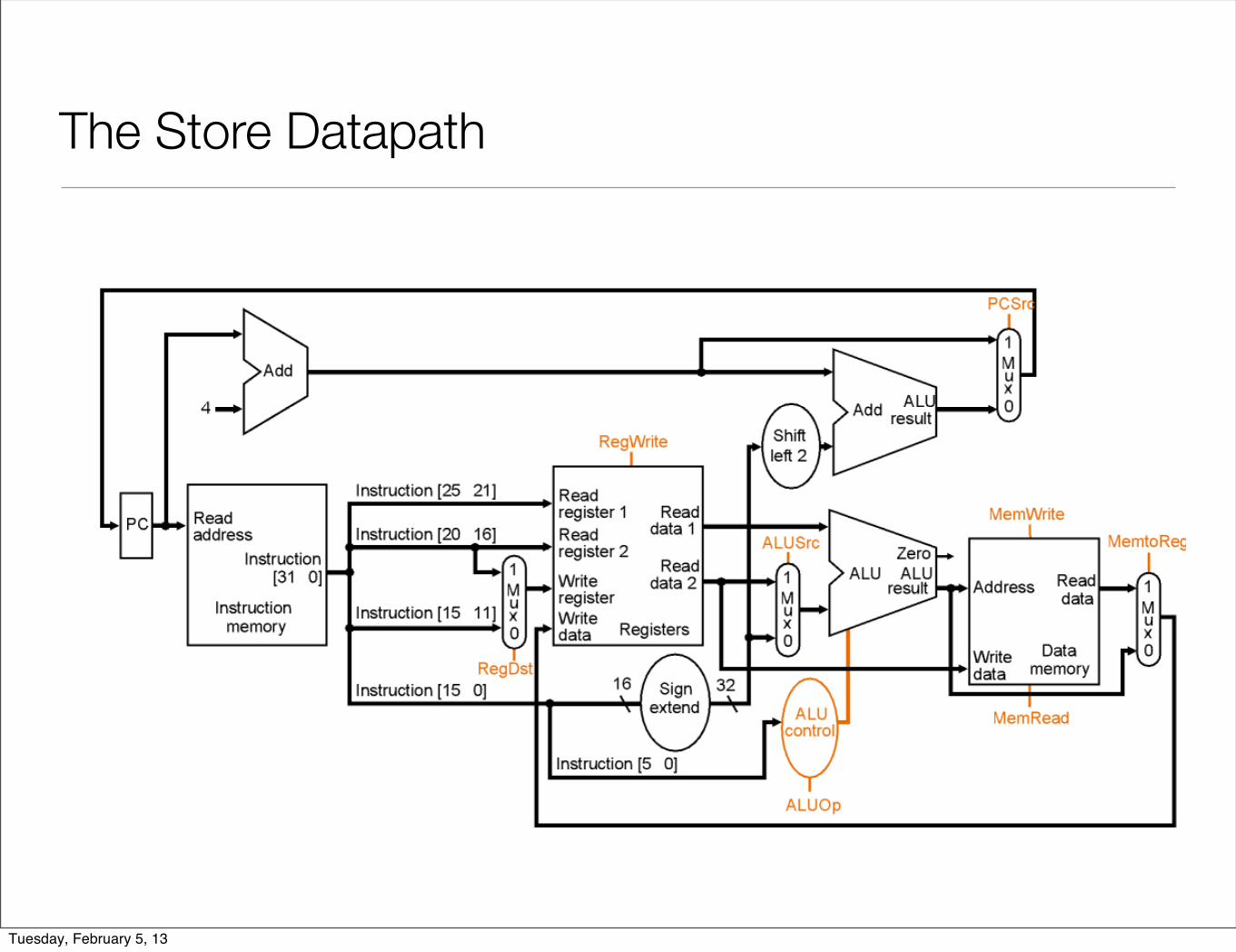
The Store Datapath
Tuesday, February 5, 13

The Store Datapath
Tuesday, February 5, 13
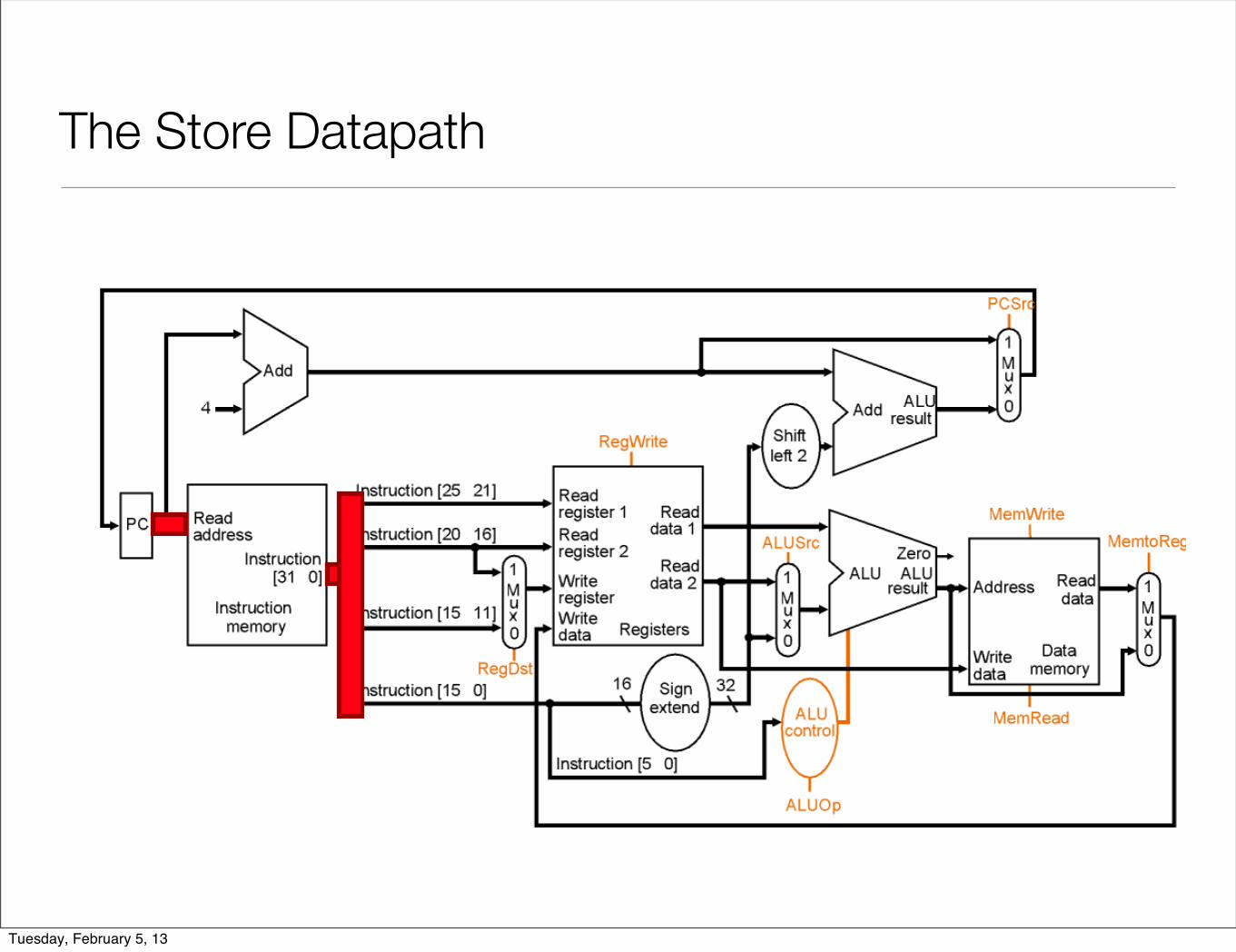
The Store Datapath
Tuesday, February 5, 13
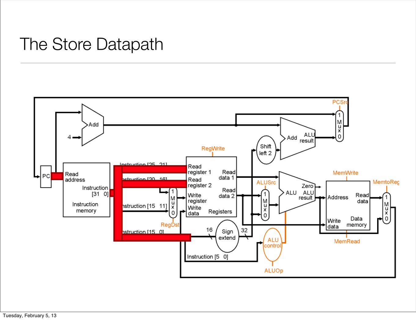
The Store Datapath
Tuesday, February 5, 13
The Store Datapath
Tuesday, February 5, 13

The Store Datapath
Tuesday, February 5, 13

The Store Datapath
Tuesday, February 5, 13
The Store Datapath
Tuesday, February 5, 13
The Store Datapath
Tuesday, February 5, 13
The Branch (beq) Datapath
Tuesday, February 5, 13
The Branch (beq) Datapath
Tuesday, February 5, 13
The Branch (beq) Datapath
Tuesday, February 5, 13
The Branch (beq) Datapath
Tuesday, February 5, 13
The Branch (beq) Datapath
Tuesday, February 5, 13
The Branch (beq) Datapath
Tuesday, February 5, 13
The Branch (beq) Datapath
Tuesday, February 5, 13
The Branch (beq) Datapath
Tuesday, February 5, 13

The Branch (beq) Datapath
Tuesday, February 5, 13
The Branch (beq) Datapath
Tuesday, February 5, 13
The Branch (beq) Datapath
Tuesday, February 5, 13
The Branch (beq) Datapath
Tuesday, February 5, 13
The Branch (beq) Datapath
Tuesday, February 5, 13
The Branch (beq) Datapath
Tuesday, February 5, 13

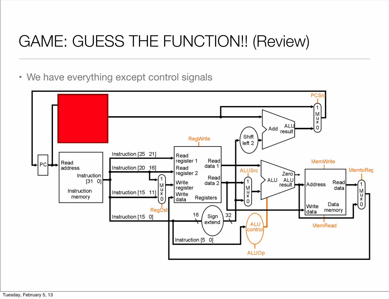
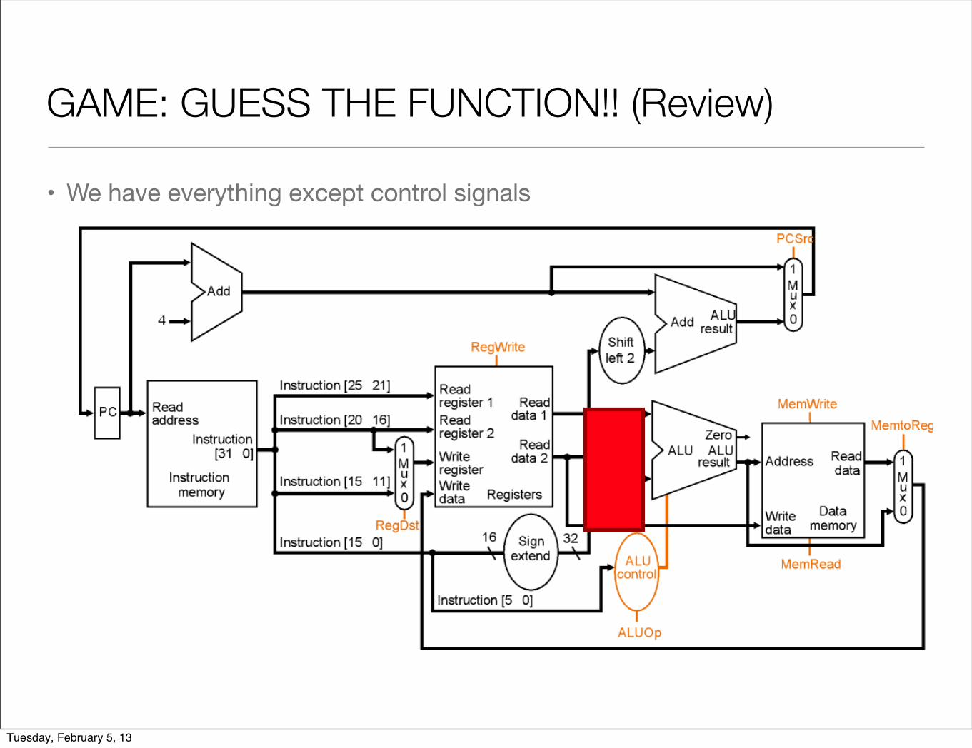
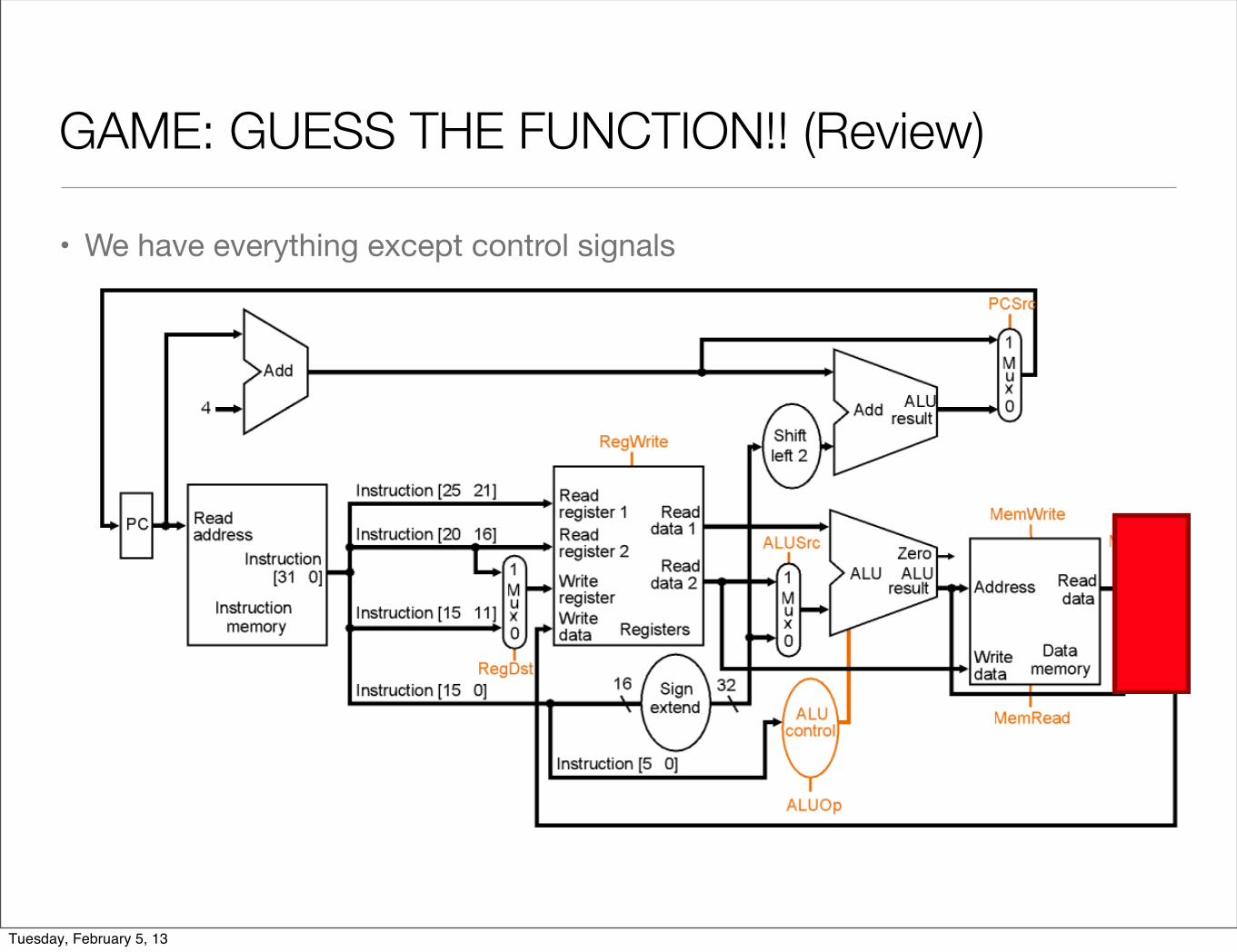
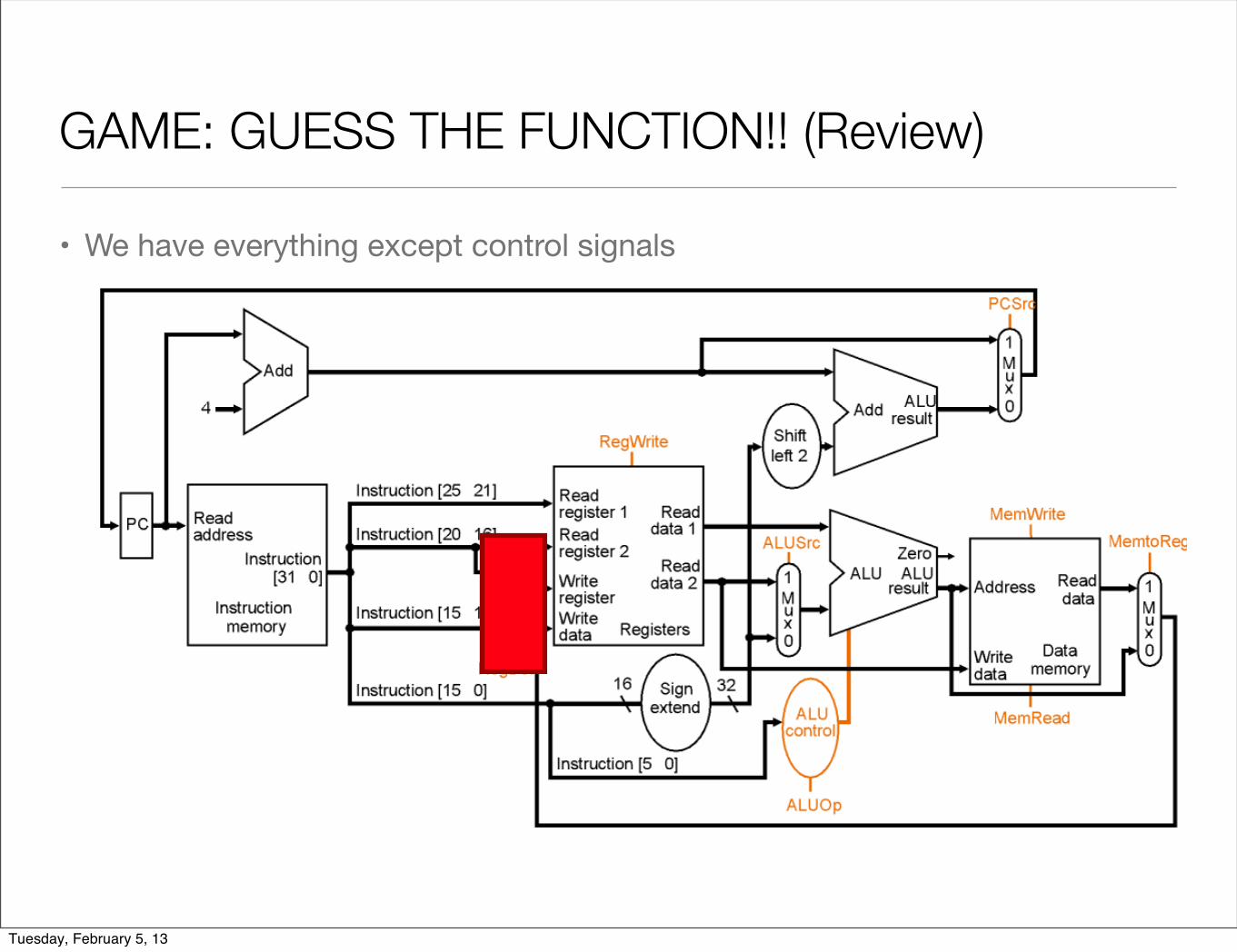
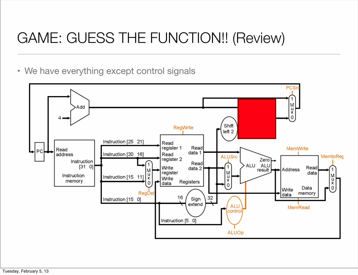
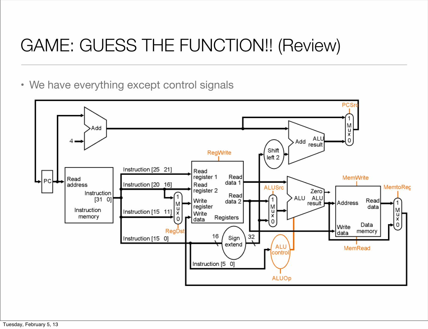
GAME: GUESS THE FUNCTION!! (Review)
• We have everything except control signals
Tuesday, February 5, 13
GAME: GUESS THE FUNCTION!! (Review)
• We have everything except control signals
Tuesday, February 5, 13
GAME: GUESS THE FUNCTION!! (Review)
• We have everything except control signals
Tuesday, February 5, 13
GAME: GUESS THE FUNCTION!! (Review)
• We have everything except control signals
Tuesday, February 5, 13
GAME: GUESS THE FUNCTION!! (Review)
• We have everything except control signals
Tuesday, February 5, 13
GAME: GUESS THE FUNCTION!! (Review)
• We have everything except control signals
Tuesday, February 5, 13

GAME: GUESS THE FUNCTION!! (Review)
• We have everything except control signals
Tuesday, February 5, 13
GAME: GUESS THE FUNCTION!! (Review)
• We have everything except control signals
Tuesday, February 5, 13

Key Points
Tuesday, February 5, 13
Key Points
• CPU is just a collection of state and combinational logic
Tuesday, February 5, 13
Key Points
• CPU is just a collection of state and combinational logic
• We just designed a very rich processor, at least in terms of functionality
Tuesday, February 5, 13
Key Points
• CPU is just a collection of state and combinational logic
• We just designed a very rich processor, at least in terms of functionality
• ET = IC * CPI * Cycle Time
• where does the single-cycle machine fit in?
Tuesday, February 5, 13

The Control Unit
Tuesday, February 5, 13

Putting it All Together: A Single Cycle Datapath
• We have everything except control signals
Tuesday, February 5, 13
Putting it All Together: A Single Cycle Datapath
Tuesday, February 5, 13
Putting it All Together: A Single Cycle Datapath
Tuesday, February 5, 13
Putting it All Together: A Single Cycle Datapath
Tuesday, February 5, 13
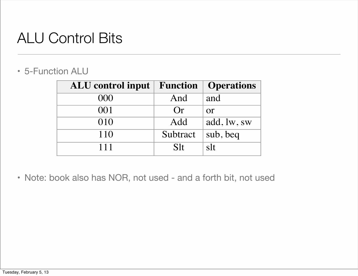
ALU Control Bits
• 5-Function ALU
• Note: book also has NOR, not used - and a forth bit, not used
ALU control input Function Operations 000 And and 001 Or or 010 Add add, lw, sw 110 Subtract sub, beq 111 Slt slt
Tuesday, February 5, 13
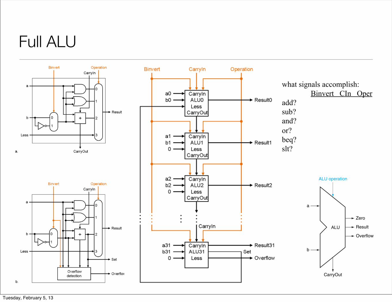
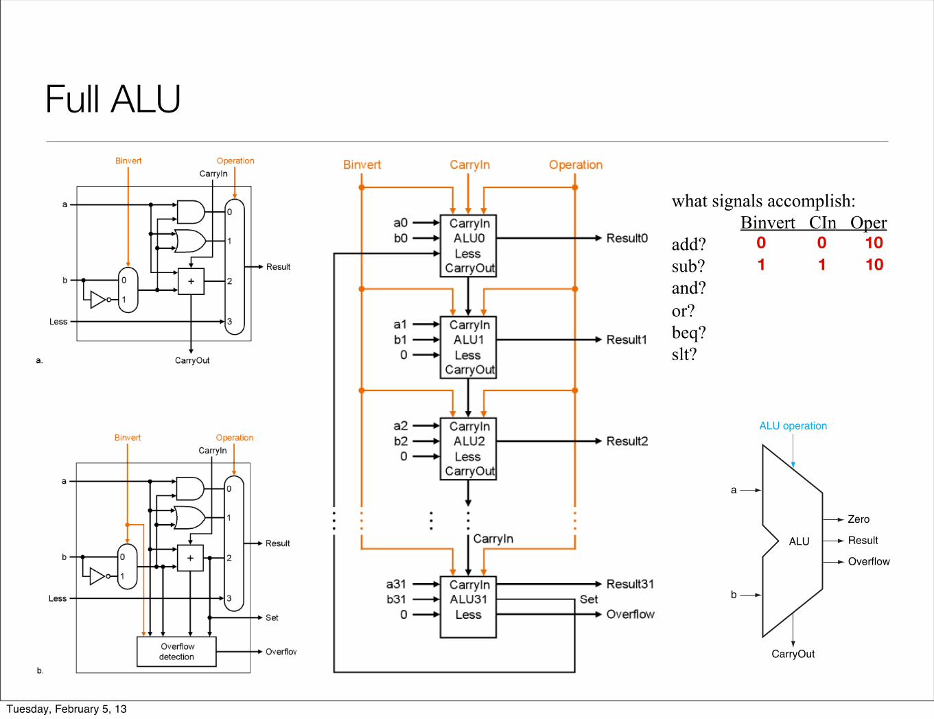
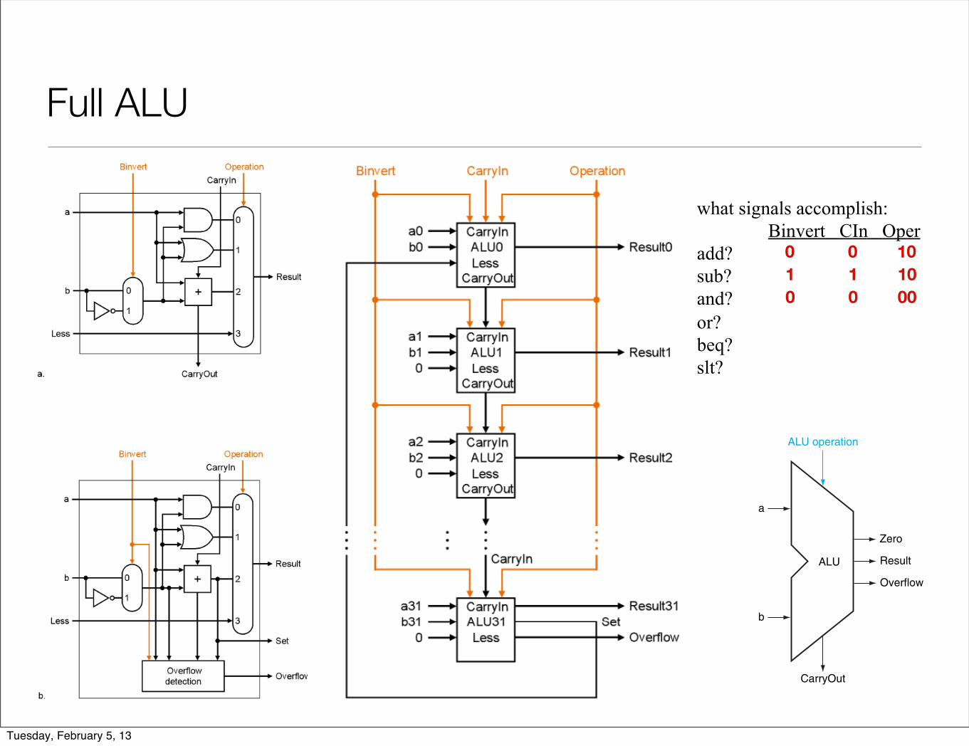
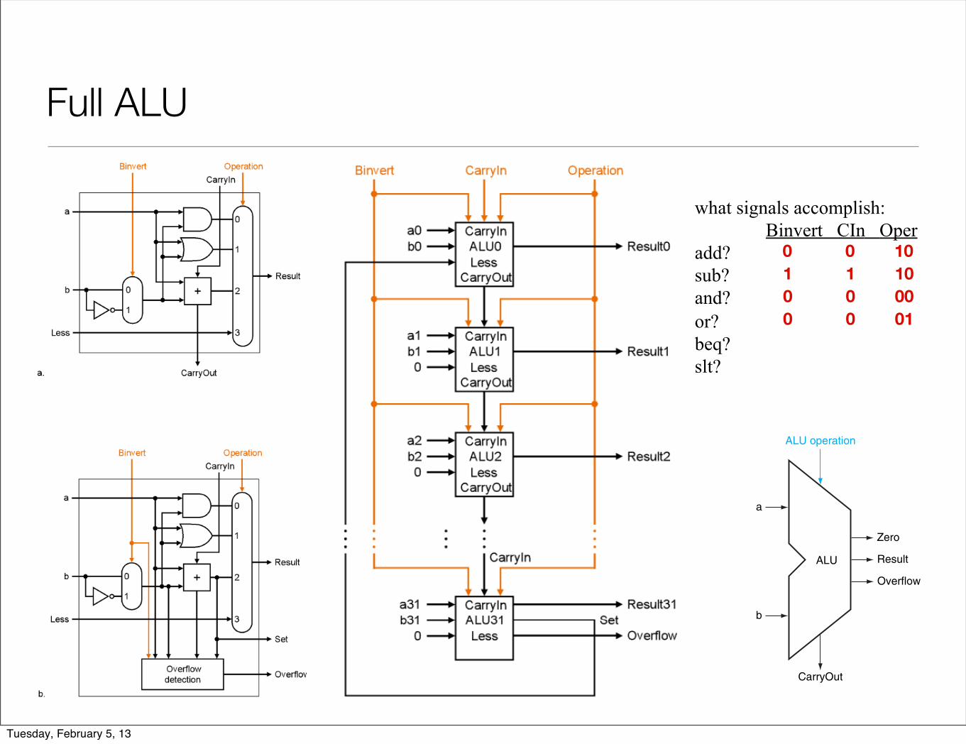
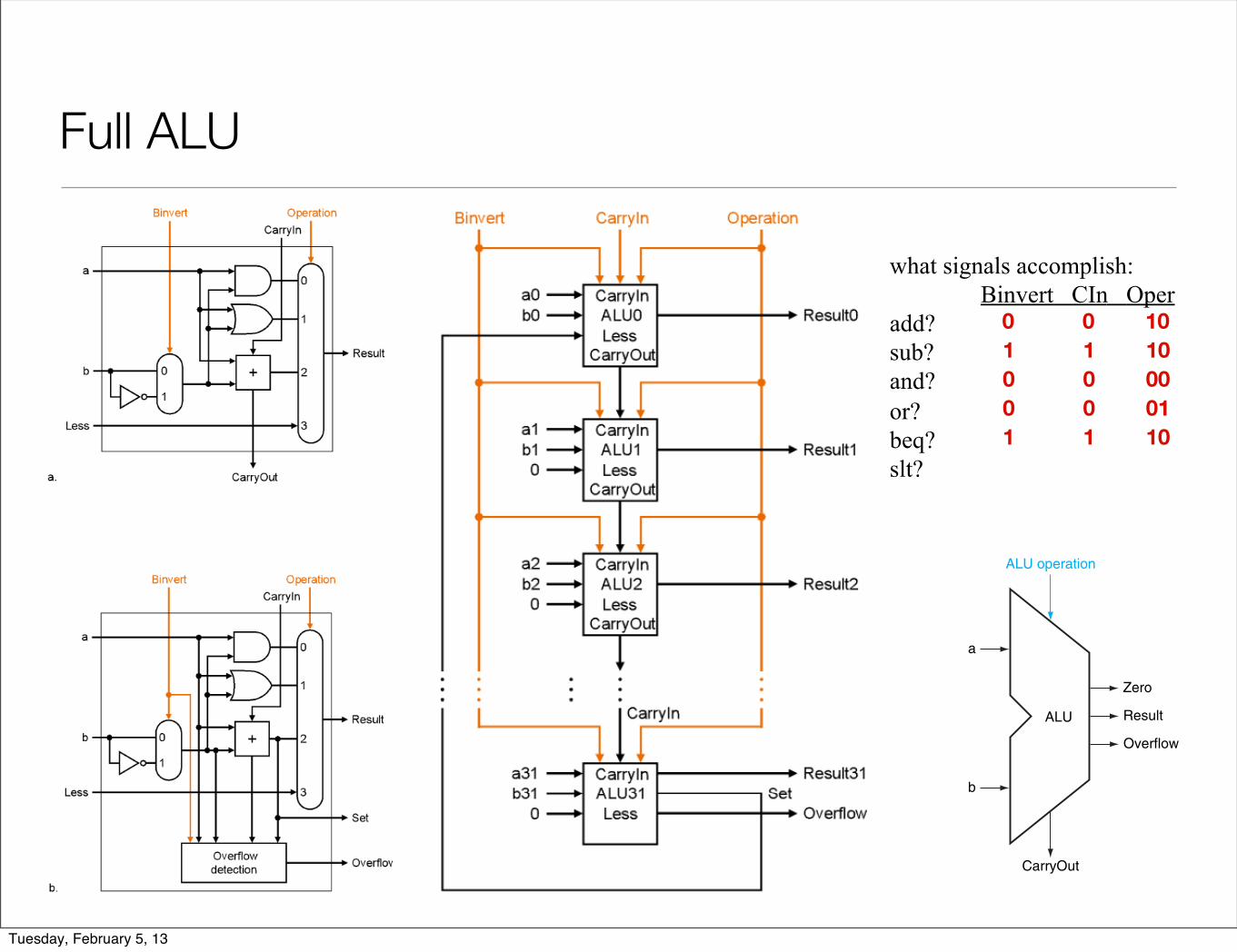
Full ALU
what signals accomplish: Binvert CIn Oper add? sub? and? or? beq? slt?
ALU
a
ALU operation
b
CarryOut
Zero
Result
Overflow
FIGURE C.5.14 The symbol commonly used to represent an ALU, as shown in Figure C.5.12. This symbol is also used to represent an adder, so it is normally labeled either with ALU or Adder.
module MIPSALU (ALUctl, A, B, ALUOut, Zero); input [3:0] ALUctl; input [31:0] A,B; output reg [31:0] ALUOut; output Zero;
assign Zero = (ALUOut==0); //Zero is true if ALUOut is 0 always @(ALUctl, A, B) begin //reevaluate if these change case (ALUctl) 0: ALUOut <= A & B; 1: ALUOut <= A | B; 2: ALUOut <= A + B; 6: ALUOut <= A - B; 7: ALUOut <= A < B ? 1 : 0; 12: ALUOut <= ~(A | B); // result is nor default: ALUOut <= 0; endcase endendmodule
FIGURE C.5.15 A Verilog behavioral defi nition of a MIPS ALU.
C.5 Constructing a Basic Arithmetic Logic Unit C-37
AppendixC-9780123747501.indd 37AppendixC-9780123747501.indd 37 26/07/11 6:28 PM26/07/11 6:28 PM
Tuesday, February 5, 13

Full ALU
what signals accomplish: Binvert CIn Oper add? sub? and? or? beq? slt?
0 0 10
ALU
a
ALU operation
b
CarryOut
Zero
Result
Overflow
FIGURE C.5.14 The symbol commonly used to represent an ALU, as shown in Figure C.5.12. This symbol is also used to represent an adder, so it is normally labeled either with ALU or Adder.
module MIPSALU (ALUctl, A, B, ALUOut, Zero); input [3:0] ALUctl; input [31:0] A,B; output reg [31:0] ALUOut; output Zero;
assign Zero = (ALUOut==0); //Zero is true if ALUOut is 0 always @(ALUctl, A, B) begin //reevaluate if these change case (ALUctl) 0: ALUOut <= A & B; 1: ALUOut <= A | B; 2: ALUOut <= A + B; 6: ALUOut <= A - B; 7: ALUOut <= A < B ? 1 : 0; 12: ALUOut <= ~(A | B); // result is nor default: ALUOut <= 0; endcase endendmodule
FIGURE C.5.15 A Verilog behavioral defi nition of a MIPS ALU.
C.5 Constructing a Basic Arithmetic Logic Unit C-37
AppendixC-9780123747501.indd 37AppendixC-9780123747501.indd 37 26/07/11 6:28 PM26/07/11 6:28 PM
Tuesday, February 5, 13
Full ALU
what signals accomplish: Binvert CIn Oper add? sub? and? or? beq? slt?
0 0 101 1 10
ALU
a
ALU operation
b
CarryOut
Zero
Result
Overflow
FIGURE C.5.14 The symbol commonly used to represent an ALU, as shown in Figure C.5.12. This symbol is also used to represent an adder, so it is normally labeled either with ALU or Adder.
module MIPSALU (ALUctl, A, B, ALUOut, Zero); input [3:0] ALUctl; input [31:0] A,B; output reg [31:0] ALUOut; output Zero;
assign Zero = (ALUOut==0); //Zero is true if ALUOut is 0 always @(ALUctl, A, B) begin //reevaluate if these change case (ALUctl) 0: ALUOut <= A & B; 1: ALUOut <= A | B; 2: ALUOut <= A + B; 6: ALUOut <= A - B; 7: ALUOut <= A < B ? 1 : 0; 12: ALUOut <= ~(A | B); // result is nor default: ALUOut <= 0; endcase endendmodule
FIGURE C.5.15 A Verilog behavioral defi nition of a MIPS ALU.
C.5 Constructing a Basic Arithmetic Logic Unit C-37
AppendixC-9780123747501.indd 37AppendixC-9780123747501.indd 37 26/07/11 6:28 PM26/07/11 6:28 PM
Tuesday, February 5, 13
Full ALU
what signals accomplish: Binvert CIn Oper add? sub? and? or? beq? slt?
0 0 101 1 100 0 00
ALU
a
ALU operation
b
CarryOut
Zero
Result
Overflow
FIGURE C.5.14 The symbol commonly used to represent an ALU, as shown in Figure C.5.12. This symbol is also used to represent an adder, so it is normally labeled either with ALU or Adder.
module MIPSALU (ALUctl, A, B, ALUOut, Zero); input [3:0] ALUctl; input [31:0] A,B; output reg [31:0] ALUOut; output Zero;
assign Zero = (ALUOut==0); //Zero is true if ALUOut is 0 always @(ALUctl, A, B) begin //reevaluate if these change case (ALUctl) 0: ALUOut <= A & B; 1: ALUOut <= A | B; 2: ALUOut <= A + B; 6: ALUOut <= A - B; 7: ALUOut <= A < B ? 1 : 0; 12: ALUOut <= ~(A | B); // result is nor default: ALUOut <= 0; endcase endendmodule
FIGURE C.5.15 A Verilog behavioral defi nition of a MIPS ALU.
C.5 Constructing a Basic Arithmetic Logic Unit C-37
AppendixC-9780123747501.indd 37AppendixC-9780123747501.indd 37 26/07/11 6:28 PM26/07/11 6:28 PM
Tuesday, February 5, 13
Full ALU
what signals accomplish: Binvert CIn Oper add? sub? and? or? beq? slt?
0 0 101 1 100 0 000 0 01
ALU
a
ALU operation
b
CarryOut
Zero
Result
Overflow
FIGURE C.5.14 The symbol commonly used to represent an ALU, as shown in Figure C.5.12. This symbol is also used to represent an adder, so it is normally labeled either with ALU or Adder.
module MIPSALU (ALUctl, A, B, ALUOut, Zero); input [3:0] ALUctl; input [31:0] A,B; output reg [31:0] ALUOut; output Zero;
assign Zero = (ALUOut==0); //Zero is true if ALUOut is 0 always @(ALUctl, A, B) begin //reevaluate if these change case (ALUctl) 0: ALUOut <= A & B; 1: ALUOut <= A | B; 2: ALUOut <= A + B; 6: ALUOut <= A - B; 7: ALUOut <= A < B ? 1 : 0; 12: ALUOut <= ~(A | B); // result is nor default: ALUOut <= 0; endcase endendmodule
FIGURE C.5.15 A Verilog behavioral defi nition of a MIPS ALU.
C.5 Constructing a Basic Arithmetic Logic Unit C-37
AppendixC-9780123747501.indd 37AppendixC-9780123747501.indd 37 26/07/11 6:28 PM26/07/11 6:28 PM
Tuesday, February 5, 13
Full ALU
what signals accomplish: Binvert CIn Oper add? sub? and? or? beq? slt?
0 0 101 1 100 0 000 0 011 1 10
ALU
a
ALU operation
b
CarryOut
Zero
Result
Overflow
FIGURE C.5.14 The symbol commonly used to represent an ALU, as shown in Figure C.5.12. This symbol is also used to represent an adder, so it is normally labeled either with ALU or Adder.
module MIPSALU (ALUctl, A, B, ALUOut, Zero); input [3:0] ALUctl; input [31:0] A,B; output reg [31:0] ALUOut; output Zero;
assign Zero = (ALUOut==0); //Zero is true if ALUOut is 0 always @(ALUctl, A, B) begin //reevaluate if these change case (ALUctl) 0: ALUOut <= A & B; 1: ALUOut <= A | B; 2: ALUOut <= A + B; 6: ALUOut <= A - B; 7: ALUOut <= A < B ? 1 : 0; 12: ALUOut <= ~(A | B); // result is nor default: ALUOut <= 0; endcase endendmodule
FIGURE C.5.15 A Verilog behavioral defi nition of a MIPS ALU.
C.5 Constructing a Basic Arithmetic Logic Unit C-37
AppendixC-9780123747501.indd 37AppendixC-9780123747501.indd 37 26/07/11 6:28 PM26/07/11 6:28 PM
Tuesday, February 5, 13

Full ALU
what signals accomplish: Binvert CIn Oper add? sub? and? or? beq? slt?
0 0 101 1 100 0 000 0 011 1 101 1 11
ALU
a
ALU operation
b
CarryOut
Zero
Result
Overflow
FIGURE C.5.14 The symbol commonly used to represent an ALU, as shown in Figure C.5.12. This symbol is also used to represent an adder, so it is normally labeled either with ALU or Adder.
module MIPSALU (ALUctl, A, B, ALUOut, Zero); input [3:0] ALUctl; input [31:0] A,B; output reg [31:0] ALUOut; output Zero;
assign Zero = (ALUOut==0); //Zero is true if ALUOut is 0 always @(ALUctl, A, B) begin //reevaluate if these change case (ALUctl) 0: ALUOut <= A & B; 1: ALUOut <= A | B; 2: ALUOut <= A + B; 6: ALUOut <= A - B; 7: ALUOut <= A < B ? 1 : 0; 12: ALUOut <= ~(A | B); // result is nor default: ALUOut <= 0; endcase endendmodule
FIGURE C.5.15 A Verilog behavioral defi nition of a MIPS ALU.
C.5 Constructing a Basic Arithmetic Logic Unit C-37
AppendixC-9780123747501.indd 37AppendixC-9780123747501.indd 37 26/07/11 6:28 PM26/07/11 6:28 PM
Tuesday, February 5, 13
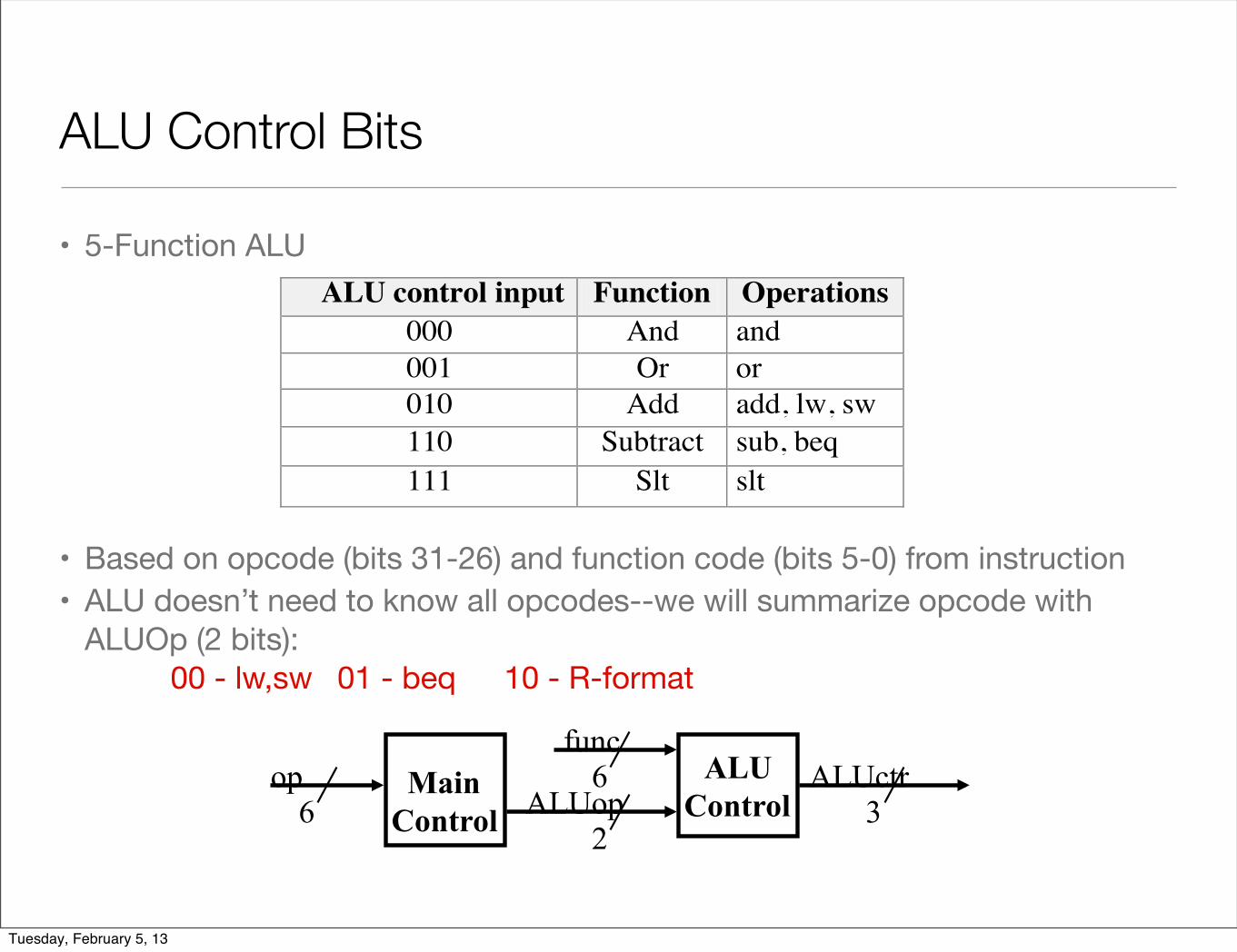
ALU Control Bits
• 5-Function ALU
• Based on opcode (bits 31-26) and function code (bits 5-0) from instruction• ALU doesn’t need to know all opcodes--we will summarize opcode with
ALUOp (2 bits): 00 - lw,sw 01 - beq 10 - R-format
ALU control input Function Operations 000 And and 001 Or or 010 Add add, lw, sw 110 Subtract sub, beq 111 Slt slt
Main Control
op 6
ALU Control
func
2
6 ALUop
ALUctr 3
Tuesday, February 5, 13

Generating ALU Control
Instructionopcode
ALUOp Instructionoperation
Functioncode
DesiredALUaction
ALUcontrolinput
lw 00 load word xxxxxx add 010
sw 00 store word xxxxxx add 010
beq 01 branch eq xxxxxx subtract 110
R-type 10 add 100000 add 010
R-type 10 subtract 100010 subtract 110
R-type 10 AND 100100 and 000
R-type 10 OR 100101 or 001
R-type 10 slt 101010 slt 111
ALU Control Logic
Tuesday, February 5, 13

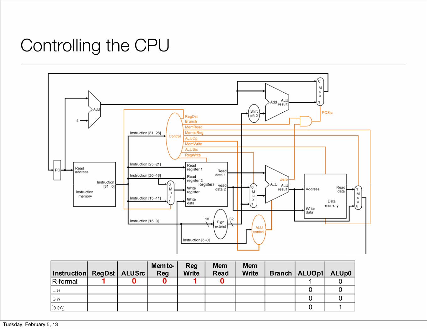
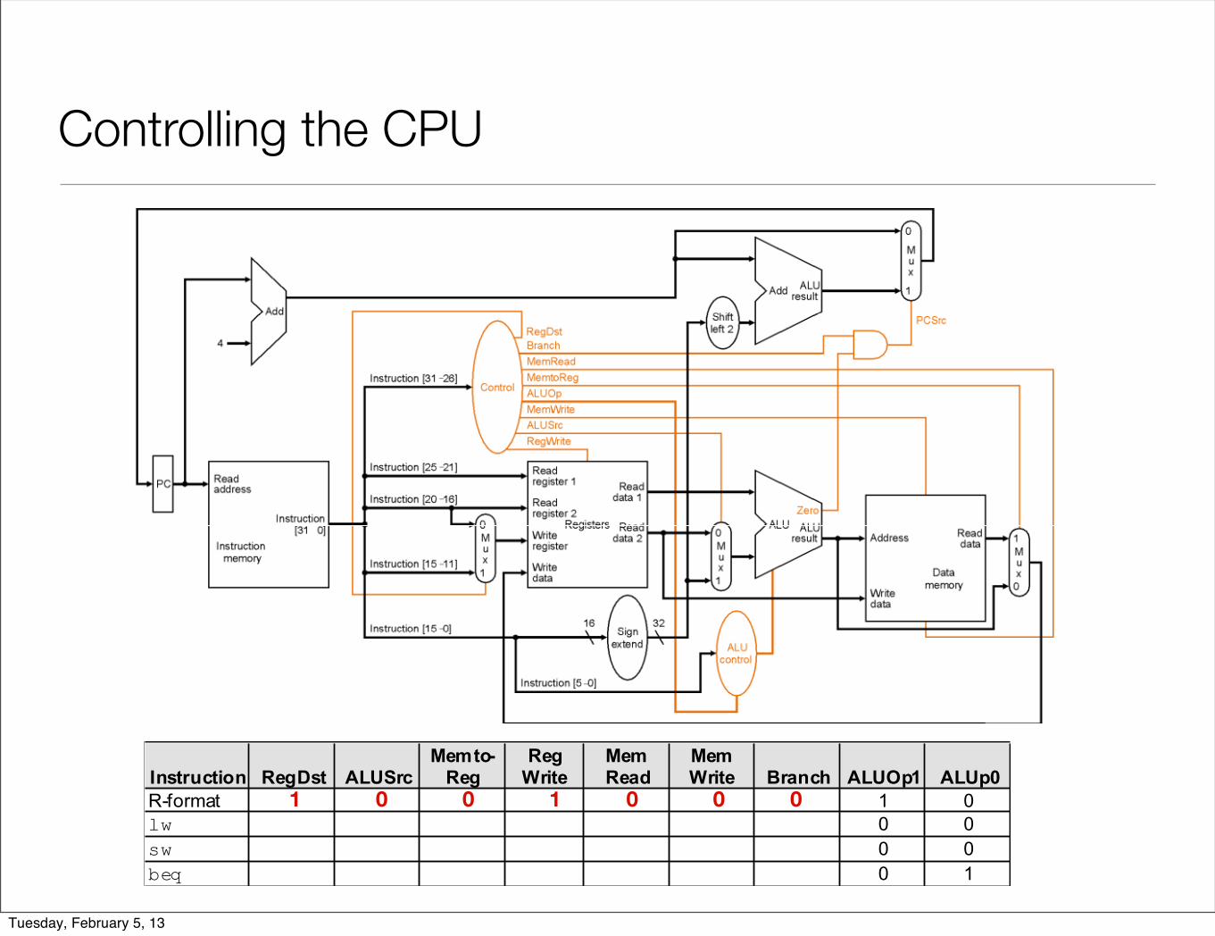
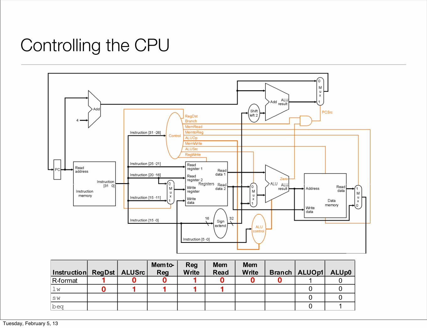
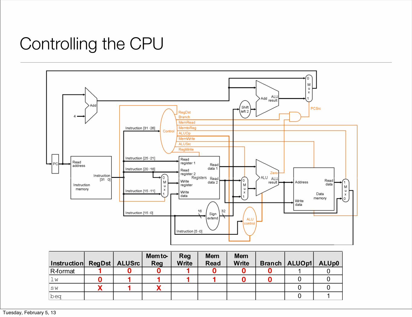
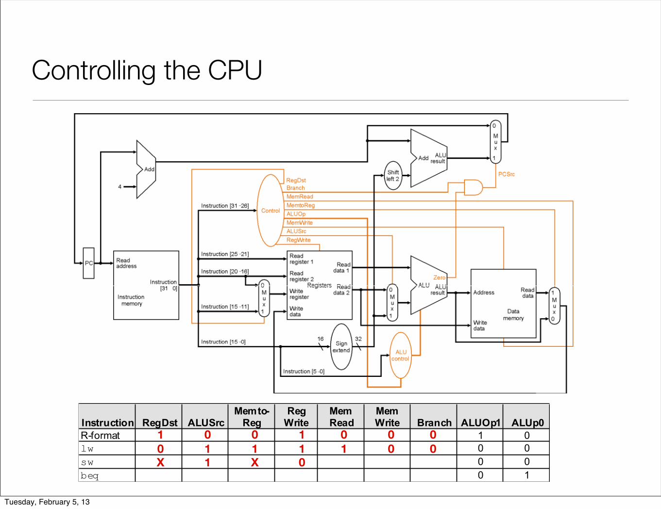
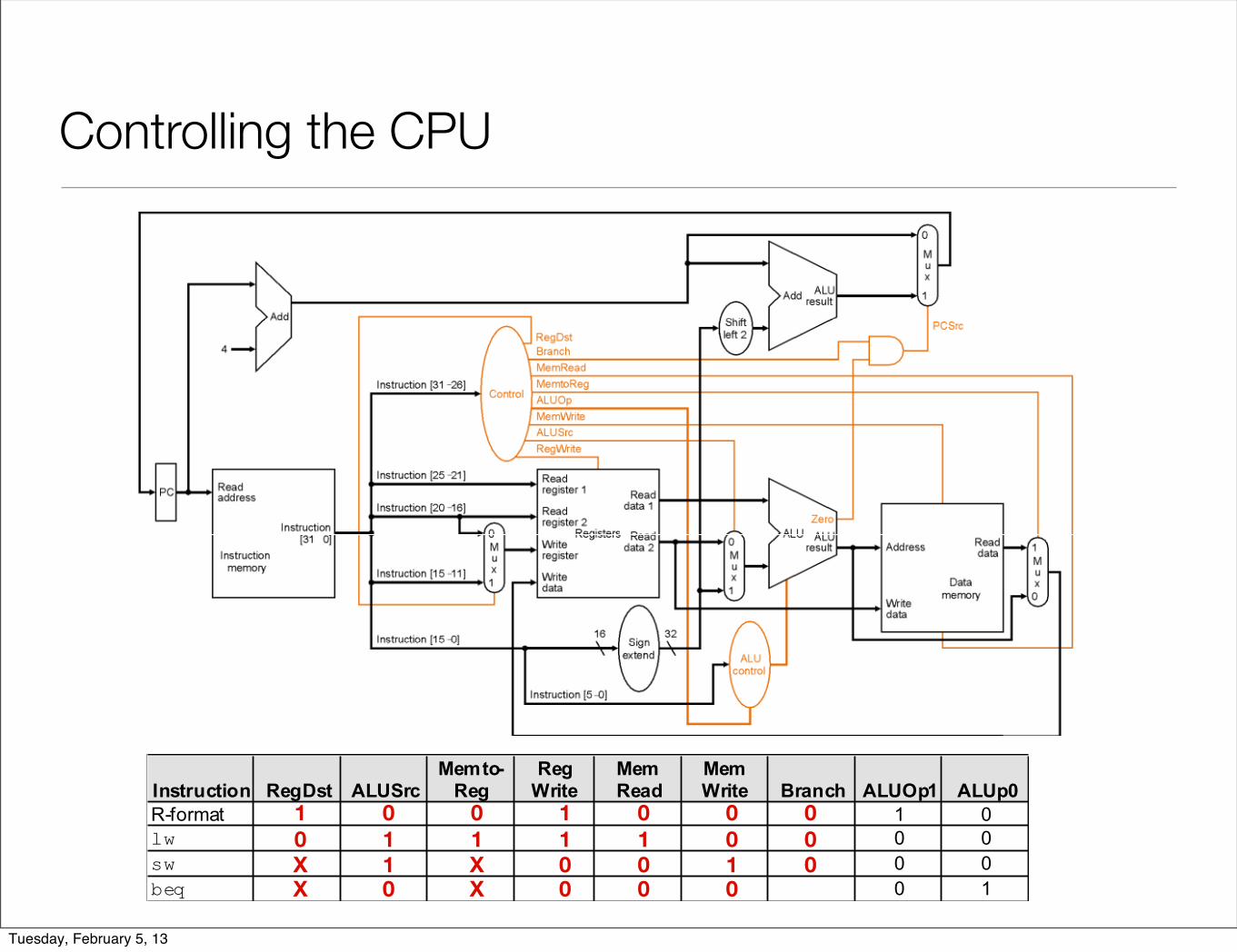
Controlling the CPU
Instruction RegDst ALUSrcMemto-
RegReg
WriteMem Read
Mem Write Branch ALUOp1 ALUp0
R-format 1 0lw 0 0sw 0 0beq 0 1
Tuesday, February 5, 13

Controlling the CPU
Instruction RegDst ALUSrcMemto-
RegReg
WriteMem Read
Mem Write Branch ALUOp1 ALUp0
R-format 1 0lw 0 0sw 0 0beq 0 1
1
Tuesday, February 5, 13

Controlling the CPU
Instruction RegDst ALUSrcMemto-
RegReg
WriteMem Read
Mem Write Branch ALUOp1 ALUp0
R-format 1 0lw 0 0sw 0 0beq 0 1
1 0
Tuesday, February 5, 13

Controlling the CPU
Instruction RegDst ALUSrcMemto-
RegReg
WriteMem Read
Mem Write Branch ALUOp1 ALUp0
R-format 1 0lw 0 0sw 0 0beq 0 1
1 0 0
Tuesday, February 5, 13

Controlling the CPU
Instruction RegDst ALUSrcMemto-
RegReg
WriteMem Read
Mem Write Branch ALUOp1 ALUp0
R-format 1 0lw 0 0sw 0 0beq 0 1
1 0 0 1
Tuesday, February 5, 13
Controlling the CPU
Instruction RegDst ALUSrcMemto-
RegReg
WriteMem Read
Mem Write Branch ALUOp1 ALUp0
R-format 1 0lw 0 0sw 0 0beq 0 1
1 0 0 1 0
Tuesday, February 5, 13

Controlling the CPU
Instruction RegDst ALUSrcMemto-
RegReg
WriteMem Read
Mem Write Branch ALUOp1 ALUp0
R-format 1 0lw 0 0sw 0 0beq 0 1
1 0 0 1 0 0
Tuesday, February 5, 13
Controlling the CPU
Instruction RegDst ALUSrcMemto-
RegReg
WriteMem Read
Mem Write Branch ALUOp1 ALUp0
R-format 1 0lw 0 0sw 0 0beq 0 1
1 0 0 1 0 0 0
Tuesday, February 5, 13

Controlling the CPU
Instruction RegDst ALUSrcMemto-
RegReg
WriteMem Read
Mem Write Branch ALUOp1 ALUp0
R-format 1 0lw 0 0sw 0 0beq 0 1
1 0 0 1 0 0 00
Tuesday, February 5, 13

Controlling the CPU
Instruction RegDst ALUSrcMemto-
RegReg
WriteMem Read
Mem Write Branch ALUOp1 ALUp0
R-format 1 0lw 0 0sw 0 0beq 0 1
1 0 0 1 0 0 00 1
Tuesday, February 5, 13

Controlling the CPU
Instruction RegDst ALUSrcMemto-
RegReg
WriteMem Read
Mem Write Branch ALUOp1 ALUp0
R-format 1 0lw 0 0sw 0 0beq 0 1
1 0 0 1 0 0 00 1 1
Tuesday, February 5, 13

Controlling the CPU
Instruction RegDst ALUSrcMemto-
RegReg
WriteMem Read
Mem Write Branch ALUOp1 ALUp0
R-format 1 0lw 0 0sw 0 0beq 0 1
1 0 0 1 0 0 00 1 1 1
Tuesday, February 5, 13
Controlling the CPU
Instruction RegDst ALUSrcMemto-
RegReg
WriteMem Read
Mem Write Branch ALUOp1 ALUp0
R-format 1 0lw 0 0sw 0 0beq 0 1
1 0 0 1 0 0 00 1 1 1 1
Tuesday, February 5, 13

Controlling the CPU
Instruction RegDst ALUSrcMemto-
RegReg
WriteMem Read
Mem Write Branch ALUOp1 ALUp0
R-format 1 0lw 0 0sw 0 0beq 0 1
1 0 0 1 0 0 00 1 1 1 1 0
Tuesday, February 5, 13

Controlling the CPU
Instruction RegDst ALUSrcMemto-
RegReg
WriteMem Read
Mem Write Branch ALUOp1 ALUp0
R-format 1 0lw 0 0sw 0 0beq 0 1
1 0 0 1 0 0 00 1 1 1 1 0 0
Tuesday, February 5, 13

Controlling the CPU
Instruction RegDst ALUSrcMemto-
RegReg
WriteMem Read
Mem Write Branch ALUOp1 ALUp0
R-format 1 0lw 0 0sw 0 0beq 0 1
1 0 0 1 0 0 00 1 1 1 1 0 0X
Tuesday, February 5, 13

Controlling the CPU
Instruction RegDst ALUSrcMemto-
RegReg
WriteMem Read
Mem Write Branch ALUOp1 ALUp0
R-format 1 0lw 0 0sw 0 0beq 0 1
1 0 0 1 0 0 00 1 1 1 1 0 0X 1
Tuesday, February 5, 13
Controlling the CPU
Instruction RegDst ALUSrcMemto-
RegReg
WriteMem Read
Mem Write Branch ALUOp1 ALUp0
R-format 1 0lw 0 0sw 0 0beq 0 1
1 0 0 1 0 0 00 1 1 1 1 0 0X 1 X
Tuesday, February 5, 13
Controlling the CPU
Instruction RegDst ALUSrcMemto-
RegReg
WriteMem Read
Mem Write Branch ALUOp1 ALUp0
R-format 1 0lw 0 0sw 0 0beq 0 1
1 0 0 1 0 0 00 1 1 1 1 0 0X 1 X 0
Tuesday, February 5, 13

Controlling the CPU
Instruction RegDst ALUSrcMemto-
RegReg
WriteMem Read
Mem Write Branch ALUOp1 ALUp0
R-format 1 0lw 0 0sw 0 0beq 0 1
1 0 0 1 0 0 00 1 1 1 1 0 0X 1 X 0 0
Tuesday, February 5, 13

Controlling the CPU
Instruction RegDst ALUSrcMemto-
RegReg
WriteMem Read
Mem Write Branch ALUOp1 ALUp0
R-format 1 0lw 0 0sw 0 0beq 0 1
1 0 0 1 0 0 00 1 1 1 1 0 0X 1 X 0 0 1
Tuesday, February 5, 13

Controlling the CPU
Instruction RegDst ALUSrcMemto-
RegReg
WriteMem Read
Mem Write Branch ALUOp1 ALUp0
R-format 1 0lw 0 0sw 0 0beq 0 1
1 0 0 1 0 0 00 1 1 1 1 0 0X 1 X 0 0 1 0
Tuesday, February 5, 13

Controlling the CPU
Instruction RegDst ALUSrcMemto-
RegReg
WriteMem Read
Mem Write Branch ALUOp1 ALUp0
R-format 1 0lw 0 0sw 0 0beq 0 1
1 0 0 1 0 0 00 1 1 1 1 0 0X 1 X 0 0 1 0X
Tuesday, February 5, 13

Controlling the CPU
Instruction RegDst ALUSrcMemto-
RegReg
WriteMem Read
Mem Write Branch ALUOp1 ALUp0
R-format 1 0lw 0 0sw 0 0beq 0 1
1 0 0 1 0 0 00 1 1 1 1 0 0X 1 X 0 0 1 0X 0
Tuesday, February 5, 13

Controlling the CPU
Instruction RegDst ALUSrcMemto-
RegReg
WriteMem Read
Mem Write Branch ALUOp1 ALUp0
R-format 1 0lw 0 0sw 0 0beq 0 1
1 0 0 1 0 0 00 1 1 1 1 0 0X 1 X 0 0 1 0X 0 X
Tuesday, February 5, 13

Controlling the CPU
Instruction RegDst ALUSrcMemto-
RegReg
WriteMem Read
Mem Write Branch ALUOp1 ALUp0
R-format 1 0lw 0 0sw 0 0beq 0 1
1 0 0 1 0 0 00 1 1 1 1 0 0X 1 X 0 0 1 0X 0 X 0
Tuesday, February 5, 13

Controlling the CPU
Instruction RegDst ALUSrcMemto-
RegReg
WriteMem Read
Mem Write Branch ALUOp1 ALUp0
R-format 1 0lw 0 0sw 0 0beq 0 1
1 0 0 1 0 0 00 1 1 1 1 0 0X 1 X 0 0 1 0X 0 X 0 0
Tuesday, February 5, 13
Controlling the CPU
Instruction RegDst ALUSrcMemto-
RegReg
WriteMem Read
Mem Write Branch ALUOp1 ALUp0
R-format 1 0lw 0 0sw 0 0beq 0 1
1 0 0 1 0 0 00 1 1 1 1 0 0X 1 X 0 0 1 0X 0 X 0 0 0
Tuesday, February 5, 13

Controlling the CPU
Instruction RegDst ALUSrcMemto-
RegReg
WriteMem Read
Mem Write Branch ALUOp1 ALUp0
R-format 1 0lw 0 0sw 0 0beq 0 1
1 0 0 1 0 0 00 1 1 1 1 0 0X 1 X 0 0 1 0X 0 X 0 0 0 1
Tuesday, February 5, 13
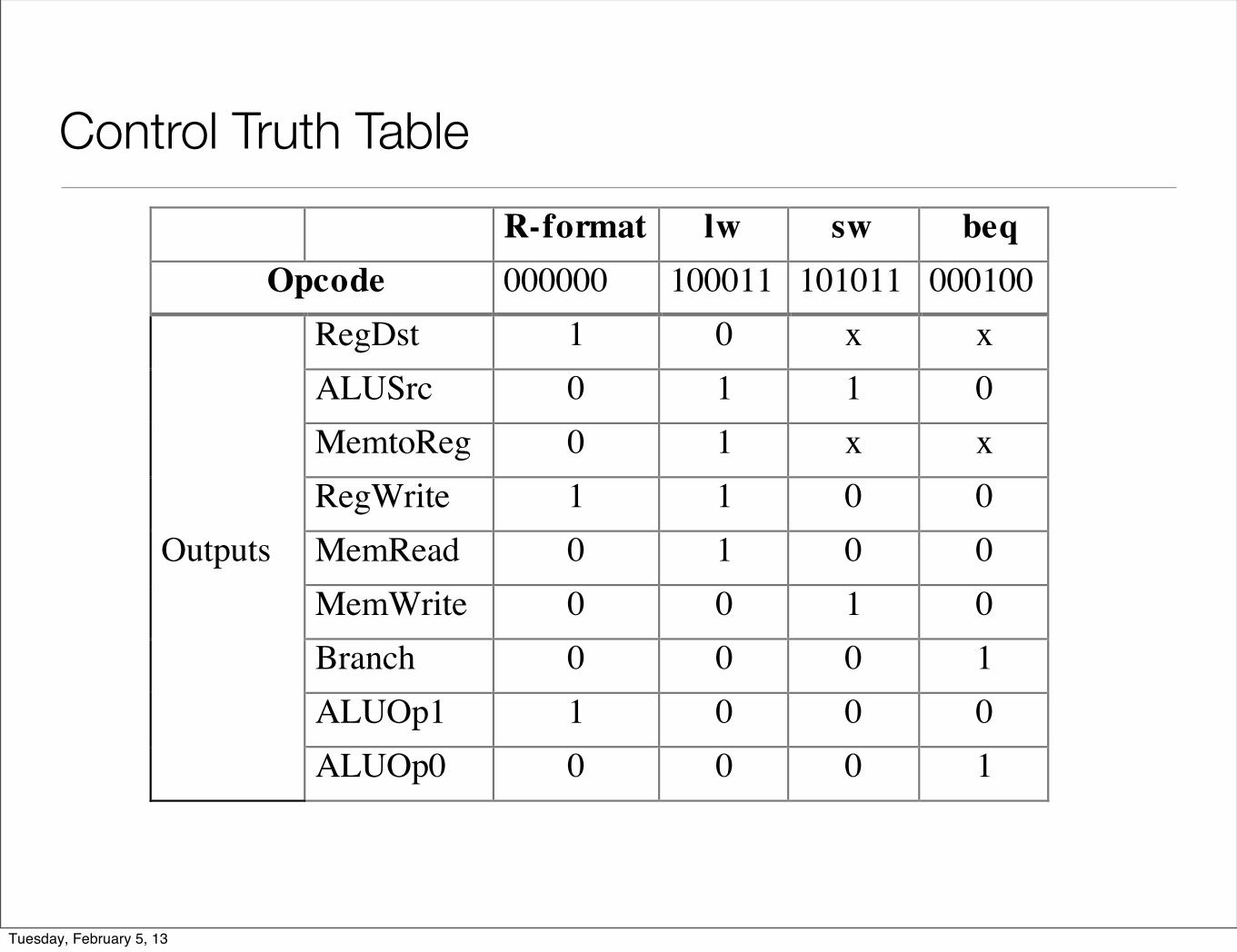
Control Truth TableR-format lw sw beq
Opcode 000000 100011 101011 000100RegDst 1 0 x xALUSrc 0 1 1 0MemtoReg 0 1 x xRegWrite 1 1 0 0
Outputs MemRead 0 1 0 0MemWrite 0 0 1 0Branch 0 0 0 1ALUOp1 1 0 0 0ALUOp0 0 0 0 1
Tuesday, February 5, 13
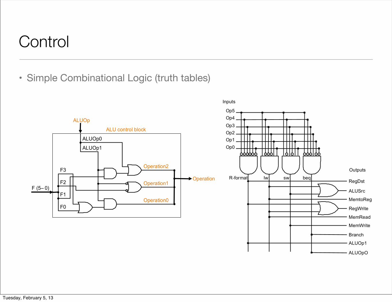
Control
• Simple Combinational Logic (truth tables)
Operation2
Operation1
Operation0
Operation
ALUOp1
F3
F2
F1
F0
F (5– 0)
ALUOp0
ALUOp
ALU control block
R-format Iw sw beq
Op0Op1Op2Op3Op4Op5
Inputs
Outputs
RegDst
ALUSrc
MemtoReg
RegWrite
MemRead
MemWrite
Branch
ALUOp1
ALUOpO
Tuesday, February 5, 13
Single Cycle CPU Summary
Tuesday, February 5, 13
Single Cycle CPU Summary
• Easy, particularly the control
Tuesday, February 5, 13
Single Cycle CPU Summary
• Easy, particularly the control
• Which instruction takes the longest? By how much? Why is that a problem?
• ET = IC * CPI * CT
Tuesday, February 5, 13
Single Cycle CPU Summary
• Easy, particularly the control
• Which instruction takes the longest? By how much? Why is that a problem?
• ET = IC * CPI * CT
• What else can we do?
Tuesday, February 5, 13
Single Cycle CPU Summary
• Easy, particularly the control
• Which instruction takes the longest? By how much? Why is that a problem?
• ET = IC * CPI * CT
• What else can we do?
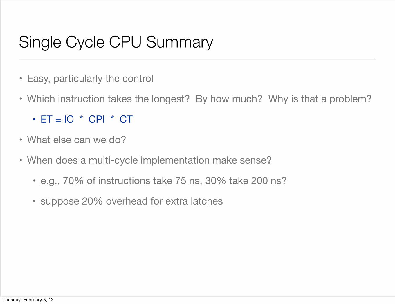
• When does a multi-cycle implementation make sense?
• e.g., 70% of instructions take 75 ns, 30% take 200 ns?
• suppose 20% overhead for extra latches
Tuesday, February 5, 13

Single Cycle CPU Summary
• Easy, particularly the control
• Which instruction takes the longest? By how much? Why is that a problem?
• ET = IC * CPI * CT
• What else can we do?
• When does a multi-cycle implementation make sense?
• e.g., 70% of instructions take 75 ns, 30% take 200 ns?
• suppose 20% overhead for extra latches
• Real machines have much more variable instruction latencies than this.
Tuesday, February 5, 13