Embed Size (px)
Citation preview
SBFS019A – JANUARY 1988 — REVISED OCTOBER 2003
www.ti.com
PRODUCTION DATA information is current as of publication date.Products conform to specifications per the terms of Texas Instrumentsstandard warranty. Production processing does not necessarily includetesting of all parameters.
Copyright © 1998-2003, Texas Instruments Incorporated
Please be aware that an important notice concerning availability, standard warranty, and use in critical applications ofTexas Instruments semiconductor products and disclaimers thereto appears at the end of this data sheet.
All trademarks are the property of their respective owners.
MPC508AMPC509A
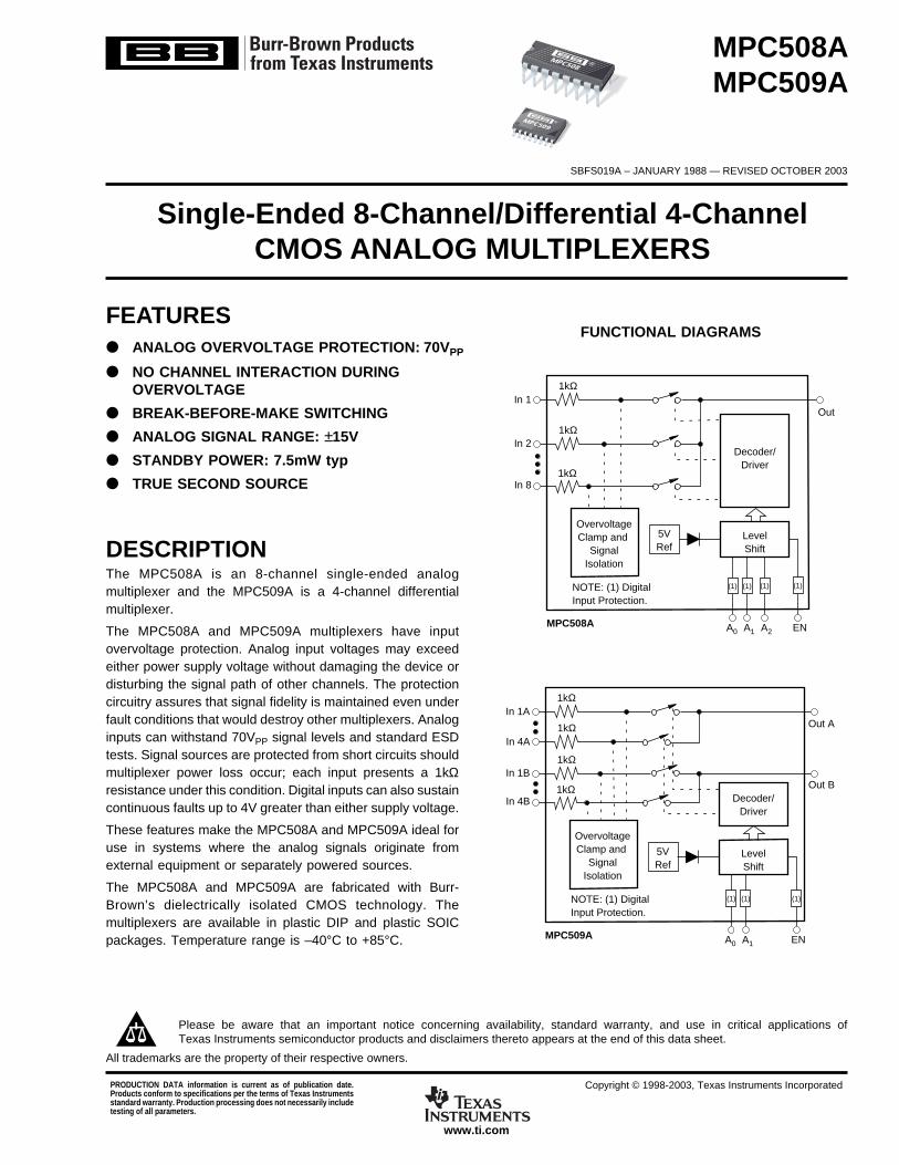
FUNCTIONAL DIAGRAMS
Single-Ended 8-Channel/Differential 4-ChannelCMOS ANALOG MULTIPLEXERS
FEATURES ANALOG OVERVOLTAGE PROTECTION: 70VPP
NO CHANNEL INTERACTION DURINGOVERVOLTAGE
BREAK-BEFORE-MAKE SWITCHING
ANALOG SIGNAL RANGE: ±15V
STANDBY POWER: 7.5mW typ
TRUE SECOND SOURCE
LevelShift
1kΩ
1kΩ
1kΩ
OvervoltageClamp and
SignalIsolation
5VRef
Decoder/Driver
NOTE: (1) DigitalInput Protection.
In 1A
In 1B
In 4B
MPC509A A0 A1 EN
Out A1kΩIn 4A
Out B
(1) (1) (1)
LevelShift
1kΩ
1kΩ
1kΩ
OvervoltageClamp and
SignalIsolation
5VRef
Decoder/Driver
NOTE: (1) DigitalInput Protection.
In 1
In 2
In 8
MPC508A A0 A1 A2 EN
(1)
Out
(1) (1) (1)
DESCRIPTIONThe MPC508A is an 8-channel single-ended analogmultiplexer and the MPC509A is a 4-channel differentialmultiplexer.
The MPC508A and MPC509A multiplexers have inputovervoltage protection. Analog input voltages may exceedeither power supply voltage without damaging the device ordisturbing the signal path of other channels. The protectioncircuitry assures that signal fidelity is maintained even underfault conditions that would destroy other multiplexers. Analoginputs can withstand 70VPP signal levels and standard ESDtests. Signal sources are protected from short circuits shouldmultiplexer power loss occur; each input presents a 1kΩresistance under this condition. Digital inputs can also sustaincontinuous faults up to 4V greater than either supply voltage.
These features make the MPC508A and MPC509A ideal foruse in systems where the analog signals originate fromexternal equipment or separately powered sources.
The MPC508A and MPC509A are fabricated with Burr-Brown’s dielectrically isolated CMOS technology. Themultiplexers are available in plastic DIP and plastic SOICpackages. Temperature range is –40°C to +85°C.
MPC508
MPC509

MPC508A, MPC509A2SBFS019Awww.ti.com
ELECTRICAL CHARACTERISTICSSupplies = +15V, –15V; VAH (Logic Level High) = +4.0V, VAL (Logic Level Low) = +0.8V, unless otherwise specified.
MPC508A/509A
PARAMETER TEMP MIN TYP MAX UNITS
ANALOG CHANNEL CHARACTERISTICSVS, Analog Signal Range Full –15 +15 VRON, On Resistance(1) +25°C 1.3 1.5 kΩ
Full 1.5 1.8 kΩIS (OFF), Off Input Leakage Current +25°C 0.5 nA
Full 10 nAID (OFF), Off Output Leakage Current +25°C 0.2 nA
MPC508A Full 5 nAMPC509A Full 5 nA
ID (OFF) with Input Overvoltage Applied(2) +25°C 2.0 µAID (ON), On Channel Leakage Current +25°C 2 nA
MPC508A Full 10 nAMPC509A Full 10 nA
IDIFF Differential Off Output Leakage Current (MPC509A Only) Full 10 nA
DIGITAL INPUT CHARACTERISTICSVAL, Input Low Threshold Drive Full 0.8 VVAH, Input High Threshold(3) Full 4.0 VIA, Input Leakage Current (High or Low)(4) Full 1.0 µA
SWITCHING CHARACTERISTICStA, Access Time +25°C 0.5 µs
Full 0.6 µstOPEN, Break-Before-Make Delay +25°C 25 80 nstON (EN), Enable Delay (ON) +25°C 200 ns
Full 500 nstOFF (EN), Enable Delay (OFF) +25°C 250 ns
Full 500 nsSettling Time (0.1%) +25°C 1.2 µs
(0.01%) +25°C 3.5 µs"OFF Isolation"(5) +25°C 50 68 dBCS (OFF), Channel Input Capacitance +25°C 5 pFCD (OFF), Channel Output Capacitance: MPC508A +25°C 25 pF
MPC509A +25°C 12 pFCA, Digital Input Capacitance 25°C 5 pFCDS (OFF), Input to Output Capacitance +25°C 0.1 pF
POWER REQUIREMENTSPD, Power Dissipation Full 7.5 mWI+, Current Pin 1(6) Full 0.7 1.5 mAI–, Current Pin 27(6) Full 5 20 µA
NOTES: (1) VOUT = ±10V, IOUT = –100µA. (2) Analog overvoltage = ±33V. (3) To drive from DTL/TTL circuits. 1kΩ pull-up resistors to +5.0V supply are recommended.(4) Digital input leakage is primarily due to the clamp diodes. Typical leakage is less than 1nA at 25°C. (5) VEN = 0.8V, RL = 1kΩ, CL = 15pF, VS = 7Vrms, f = 100kHz.Worst-case isolation occurs on channel 4 due to proximity of the output pins. (6) VEN, VA = 0V or 4.0V.
MPC508A, MPC509A 3SBFS019A www.ti.com
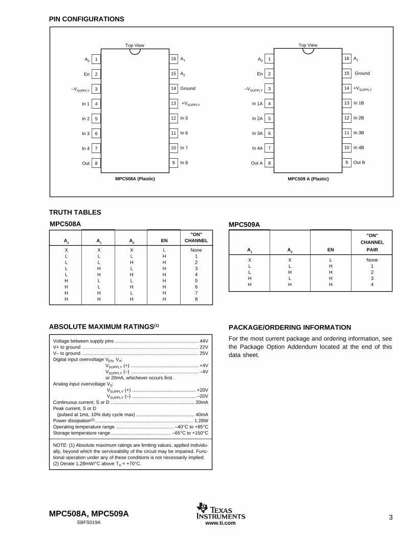
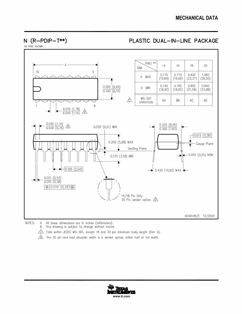
PIN CONFIGURATIONS
TRUTH TABLES
"ON"A2 A1 A0 EN CHANNEL
X X X L NoneL L L H 1L L H H 2L H L H 3L H H H 4H L L H 5H L H H 6H H L H 7H H H H 8
MPC508A MPC509A
"ON"CHANNEL
A1 A0 EN PAIR
X X L NoneL L H 1L H H 2H L H 3H H H 4
Voltage between supply pins ............................................................... 44VV+ to ground ........................................................................................ 22VV– to ground ........................................................................................ 25VDigital input overvoltage VEN, VA:
VSUPPLY (+) ................................................... +4VVSUPPLY (–) ................................................... –4Vor 20mA, whichever occurs first.
Analog input overvoltage VS:VSUPPLY (+) ................................................ +20VVSUPPLY (–) ................................................ –20V
Continuous current, S or D ............................................................... 20mAPeak current, S or D
(pulsed at 1ms, 10% duty cycle max) ............................................ 40mAPower dissipation(2) .......................................................................... 1.28WOperating temperature range ........................................... –40°C to +85°CStorage temperature range ............................................. –65°C to +150°C
NOTE: (1) Absolute maximum ratings are limiting values, applied individu-ally, beyond which the serviceability of the circuit may be impaired. Func-tional operation under any of these conditions is not necessarily implied.(2) Derate 1.28mW/°C above TA = +70°C.
ABSOLUTE MAXIMUM RATINGS(1)
1
2
3
4
5
6
7
8
16
15
14
13
12
11
10
9
A0
En
–VSUPPLY
In 1
In 2
In 3
In 4
Out
A1
A2
Ground
+VSUPPLY
In 5
In 6
In 7
In 8
Top View
MPC508A (Plastic)
1
2
3
4
5
6
7
8
16
15
14
13
12
11
10
9
A0
En
–VSUPPLY
In 1A
In 2A
In 3A
In 4A
Out A
A1
Ground
+VSUPPLY
In 1B
In 2B
In 3B
In 4B
Out B
Top View
MPC509 A (Plastic)
PACKAGE/ORDERING INFORMATION
For the most current package and ordering information, seethe Package Option Addendum located at the end of thisdata sheet.
MPC508A, MPC509A4SBFS019Awww.ti.com
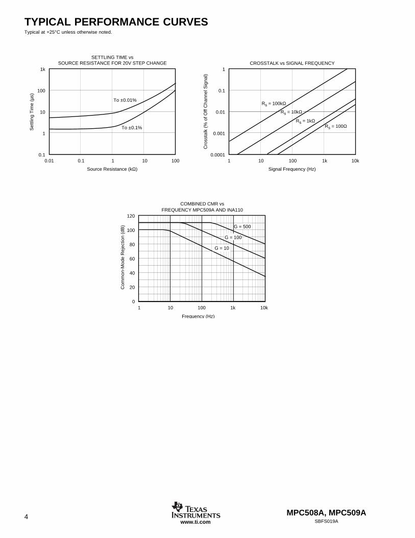
COMBINED CMR vsFREQUENCY MPC509A AND INA110
120
100
80
60
40
20
01 10 100 1k 10k
Frequency (Hz)
Com
mon
-Mod
e R
ejec
tion
(dB
) G = 500
G = 100
G = 10
CROSSTALK vs SIGNAL FREQUENCY1
0.1
0.01
0.001
0.00011 10 100 1k 10k
Signal Frequency (Hz)
Cro
ssta
lk (
% o
f Off
Cha
nnel
Sig
nal)
Rs = 100kΩ
Rs = 1kΩRs = 100Ω
Rs = 10kΩ
SETTLING TIME vsSOURCE RESISTANCE FOR 20V STEP CHANGE
1k
100
10
1
0.10.01 0.1 1 10 100
Source Resistance (kΩ)
Set
tling
Tim
e (µ
s)
To ±0.01%
To ±0.1%
TYPICAL PERFORMANCE CURVESTypical at +25°C unless otherwise noted.
MPC508A, MPC509A 5SBFS019A www.ti.com
Differential Multiplexer Static Accuracy
Static accuracy errors in a differential multiplexer are diffi-cult to control, especially when it is used for multiplexinglow-level signals with full-scale ranges of 10mV to 100mV.
The matching properties of the multiplexer, source andoutput load play a very important part in determining thetransfer accuracy of the multiplexer. The source impedanceunbalance, common-mode impedance, load bias current mis-match, load differential impedance mismatch, and common-mode impedance of the load all contribute errors to themultiplexer. The multiplexer ON resistance mismatch, leak-age current mismatch and ON resistance also contribute todifferential errors.
The effects of these errors can be minimized by following thegeneral guidelines described in this section, especially forlow-level multiplexing applications. Refer to Figure 2.
Load (Output Device) Characteristics
• Use devices with very low bias current. Generally, FETinput amplifiers should be used for low-level signals lessthan 50mV FSR. Low bias current bipolar input amplifi-ers are acceptable for signal ranges higher than 50mVFSR. Bias current matching will determine the inputoffset.
• The system dc common-mode rejection (CMR) can neverbe better than the combined CMR of the multiplexer anddriven load. System CMR will be less than the devicewhich has the lower CMR figure.
• Load impedances, differential and common-mode, shouldbe 1010Ω or higher.
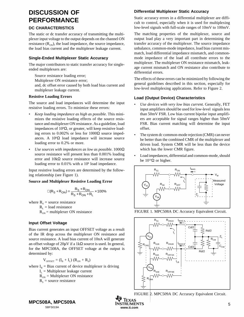
DISCUSSION OFPERFORMANCEDC CHARACTERISTICS
The static or dc transfer accuracy of transmitting the multi-plexer input voltage to the output depends on the channel ONresistance (RON), the load impedance, the source impedance,the load bias current and the multiplexer leakage current.
Single-Ended Multiplexer Static Accuracy
The major contributors to static transfer accuracy for single-ended multiplexers are:
Source resistance loading error;Multiplexer ON resistance error;and, dc offset error caused by both load bias current andmultiplexer leakage current.
Resistive Loading Errors
The source and load impedances will determine the inputresistive loading errors. To minimize these errors:
• Keep loading impedance as high as possible. This mini-mizes the resistive loading effects of the source resis-tance and multiplexer ON resistance. As a guideline, loadimpedances of 108Ω, or greater, will keep resistive load-ing errors to 0.002% or less for 1000Ω source imped-ances. A 106Ω load impedance will increase sourceloading error to 0.2% or more.
• Use sources with impedances as low as possible. 1000Ωsource resistance will present less than 0.001% loadingerror and 10kΩ source resistance will increase sourceloading error to 0.01% with a 108 load impedance.
Input resistive loading errors are determined by the follow-ing relationship (see Figure 1).
Source and Multiplexer Resistive Loading Error
∈ + = ++ +
×( ) %R RR R
R R RS ONS ON
S ON L100
where RS = source resistanceRL = load resistanceRON = multiplexer ON resistance
Input Offset Voltage
Bias current generates an input OFFSET voltage as a resultof the IR drop across the multiplexer ON resistance andsource resistance. A load bias current of 10nA will generatean offset voltage of 20µV if a 1kΩ source is used. In general,for the MPC508A, the OFFSET voltage at the output isdetermined by:
VOFFSET = (IB + IL) (RON + RS)
where IB = Bias current of device multiplexer is drivingIL = Multiplexer leakage currentRON = Multiplexer ON resistanceRS = source resistance
ZL
RS4A
RS48
ROFF4A
ROFF4B
CCM
RS1
RS1B
RON1A
RON1B
IL
Cd/2
Cd/2
RCM
Rd/2
Rd/2
IBIAS A
IBIAS B
RCM4
RCM1
VS1
VS8
ILB
FIGURE 2. MPC509A DC Accuracy Equivalent Circuit.
RS1
RS8
RON
ROFFVS1
VS8ZL
MeasuredVoltage
IL
VM
IBIAS
FIGURE 1. MPC508A DC Accuracy Equivalent Circuit.
MPC508A, MPC509A6SBFS019Awww.ti.com
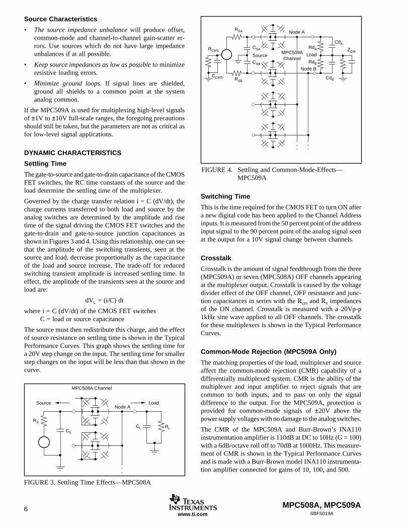
Source
Node A
CSB
RSA
ZCM
CdA
CdB
CSA
RSB
RCMS
CCMS
Node B
MPC509AChannel
RdA
RdB
Load
LoadSourceNode A
CS
RS
RLCL
MPC508A Channel
Source Characteristics
• The source impedance unbalance will produce offset,common-mode and channel-to-channel gain-scatter er-rors. Use sources which do not have large impedanceunbalances if at all possible.
• Keep source impedances as low as possible to minimizeresistive loading errors.
• Minimize ground loops. If signal lines are shielded,ground all shields to a common point at the systemanalog common.
If the MPC509A is used for multiplexing high-level signalsof ±1V to ±10V full-scale ranges, the foregoing precautionsshould still be taken, but the parameters are not as critical asfor low-level signal applications.
DYNAMIC CHARACTERISTICS
Settling Time
The gate-to-source and gate-to-drain capacitance of the CMOSFET switches, the RC time constants of the source and theload determine the settling time of the multiplexer.
Governed by the charge transfer relation i = C (dV/dt), thecharge currents transferred to both load and source by theanalog switches are determined by the amplitude and risetime of the signal driving the CMOS FET switches and thegate-to-drain and gate-to-source junction capacitances asshown in Figures 3 and 4. Using this relationship, one can seethat the amplitude of the switching transients, seen at thesource and load, decrease proportionally as the capacitanceof the load and source increase. The trade-off for reducedswitching transient amplitude is increased settling time. Ineffect, the amplitude of the transients seen at the source andload are:
dVL = (i/C) dt
where i = C (dV/dt) of the CMOS FET switches C = load or source capacitance
The source must then redistribute this charge, and the effectof source resistance on settling time is shown in the TypicalPerformance Curves. This graph shows the settling time fora 20V step change on the input. The settling time for smallerstep changes on the input will be less than that shown in thecurve.
Switching Time
This is the time required for the CMOS FET to turn ON aftera new digital code has been applied to the Channel Addressinputs. It is measured from the 50 percent point of the addressinput signal to the 90 percent point of the analog signal seenat the output for a 10V signal change between channels.
Crosstalk
Crosstalk is the amount of signal feedthrough from the three(MPC509A) or seven (MPC508A) OFF channels appearingat the multiplexer output. Crosstalk is caused by the voltagedivider effect of the OFF channel, OFF resistance and junc-tion capacitances in series with the RON and RS impedancesof the ON channel. Crosstalk is measured with a 20Vp-p1kHz sine wave applied to all OFF channels. The crosstalkfor these multiplexers is shown in the Typical PerformanceCurves.
Common-Mode Rejection (MPC509A Only)
The matching properties of the load, multiplexer and sourceaffect the common-mode rejection (CMR) capability of adifferentially multiplexed system. CMR is the ability of themultiplexer and input amplifier to reject signals that arecommon to both inputs, and to pass on only the signaldifference to the output. For the MPC509A, protection isprovided for common-mode signals of ±20V above thepower supply voltages with no damage to the analog switches.
The CMR of the MPC509A and Burr-Brown’s INA110instrumentation amplifier is 110dB at DC to 10Hz (G = 100)with a 6dB/octave roll off to 70dB at 1000Hz. This measure-ment of CMR is shown in the Typical Performance Curvesand is made with a Burr-Brown model INA110 instrumenta-tion amplifier connected for gains of 10, 100, and 500.
FIGURE 3. Settling Time Effects—MPC508A
FIGURE 4. Settling and Common-Mode-Effects—MPC509A
MPC508A, MPC509A 7SBFS019A www.ti.com
SWITCHING WAVEFORMS
Typical at +25°C, unless otherwise noted.
100ns/Div
1 On
VA Input2V/Div
Output0.5V/Div
VAM 4.0V
Address Drive(VA)
Output
50% 50%
tOPEN
0V
MPC508A(1)
GND
In 2 Thru In 7
In 1
In 8
Out
A2
A1A0
En
1kΩ
50Ω
+5V
+4.0V12.5pF
VA
VOUT
NOTE: (1) Similar connection for MPC509A.
BREAK-BEFORE-MAKE DELAY (tOPEN)
ENABLE DELAY (tON (EN), tOFF (EN))
100ns/Div
Output2V/Div
MPC508A(1)
GND
In 2 Thru In 8
In 1
Out
A2
A1A0
En
1kΩ
+10V
12.5pF
NOTE: (1) Similar connection for MPC509A.
50Ω
VA
Enable Drive
VAM 4.0V
50%
90%
90%
0V
Output
tON(EN)tOFF(EN)
Enable Drive2V/Div
Factors which will degrade multiplexer and system DC CMRare:
• Amplifier bias current and differential impedance mis-match
• Load impedance mismatch
• Multiplexer impedance and leakage current mismatch
• Load and source common-mode impedance
AC CMR roll off is determined by the amount of common-mode capacitances (absolute and mismatch) from each signalline to ground. Larger capacitances will limit CMR at higherfrequencies; thus, if good CMR is desired at higher frequen-cies, the common-mode capacitances and unbalance of sig-nal lines and multiplexer-to-amplifier wiring must be mini-mized. Use twisted-shielded-pair signal lines wherever pos-sible.
MPC508A, MPC509A8SBFS019Awww.ti.com
8
6
4
2
0100 1k 10k 100k 1M 10M
Toggle Frequency (Hz)
Sup
ply
Cur
rent
(m
A)
VS = ±10V
MPC508A(1)
GND
In 2 Thru In 7
En
In 8
Out
A2
A1A0
En
10MΩ+4V14pF
NOTE: (1) Similar connection for MPC509A.
A
A
–ISUPPLY
–15V/–10V
±10V/±5V–V
+ISUPPLY
+15V/+10V
50Ω
VA
SUPPLY CURRENT vs TOGGLE FREQUENCY
VS = ±15V
±10V/±5V
±10V/±5V
PERFORMANCE CHARACTERISTICS AND TEST CIRCUITSUnless otherwise specified: T
A = +25, V
S = ±15V, V
AM = +4V, V
AL = 0.8V.
1.4
1.3
1.2
1.1
1.0
0.9
0.8
0.7
0.6
–10 –8 –6 –4 –2 0 2 4 6 8 10
On
Res
ista
nce
(kΩ
)
ON RESISTANCE vsANALOG INPUT VOLTAGE
NORMALIZED ON RESISTANCEvs SUPPLY VOLTAGE
1.6
1.5
1.4
1.3
1.2
1.1
1.0
0.9
0.8
±5 ±6 ±7 ±8 ±9 ±10 ±11 ±12 ±13 ±14 ±15
Supply Voltage (V)
Nor
mal
ized
On
Res
ista
nce
(Ref
erre
d to
Val
ue a
t ±15
V)
±125°C > TA > –55°CVIN = +5V
ON RESISTANCE vs ANALOG INPUT SIGNAL, SUPPLY VOLTAGE 100µA
V2RON = V2/100µA
InOut
VIN
Analog Input (V)
TA = +125°C
TA = +25°C
TA = –55°C
MPC508A, MPC509A 9SBFS019A www.ti.com
Out
±10V
A
En +0.8V
ID (Off)
10V
Out
±10V
A ID (On)En
A0 A1
100nA
10nA
1nA
100pA
10pA25 50 75 100 125
Temperature (°C)
Leak
age
Cur
rent
LEAKAGE CURRENT vs TEMPERATURE
NOTE: (1) Two measurements per channel: +10V/–10V and –10V/+10V. (Two measurements per device for ID (Off): +10V/–10V and –10V/+10V).
+4.0V
± 10V±
Out
10V
IS (Off)
±10V
A
En+0.8V±
Off OutputCurrentID (Off)
Off InputLeakage Current
IS (Off)
On LeakageCurrent ID (On)
Analog Input Overvoltage (V)
+12 +15 +18 +21 +24 +27 +30 +33 +36
7
6
5
4
3
2
1
0
Ana
log
Inpu
t Cur
rent
(m
A)
Out
put O
ff Le
akag
e C
urre
nt (
nA)
Analog InputCurrent (IIN)
Output OffLeakage Current
IO (Off)
IINIO (Off)
A
+VIN
ANALOG INPUT OVERVOLTAGE CHARACTERISTICS
21
18
12
9
6
3
0
15
A
Analog Input Overvoltage (V)
−12 −15 −18 −21 −24 −27 −30 −33 −36
4
2
0
Ana
log
Inpu
t Cur
rent
(m
A)
Out
put O
ff Le
akag
e C
urre
nt (
µA)
Analog InputCurrent (IIN)
Output OffLeakage Current
IO (Off)
IINIO (Off)
A
−VIN
21
18
12
9
6
3
0
15
A
Positive Input Overvoltage
Negative Input Overvoltage
PERFORMANCE CHARACTERISTICS AND TEST CIRCUITS (CONT)
MPC508A, MPC509A10SBFS019Awww.ti.com
PERFORMANCE CHARACTERISTICS AND TEST CIRCUITS (CONT)
A
±VIN
VIN –Voltage Across Switch (V)
0 ±2 ±4 ±6 ±8 ±10 ±12 ±14 ±16
±14
±12
±10
±8
±6
±4
±2
0
Sw
itch
Cur
rent
(m
A)
ON-CHANNEL CURRENT vs VOLTAGE
–55°C +25°C
+125°C
ACCESS TIME WAVEFORM
VA Input2V/Div
Output A5V/Div
200ns/Div
VAM 4.0V
0V
10V
tA
50%
10V
90%
AddressDrive (VA)
Output A
MPC508A(1)
GND
In 2 ThruIn 7
In 1
In 8
Out
A2
A1A0
En
10MΩ
50Ω
+4V14pF
VA
NOTE: (1) Similar connection for MPC509A.
–10V
1000
900
800
700
600
500
400
3003 4 5 6 7 8 9 10 11 12 13 14 15
Logic Level High (V)
Acc
ess
Tim
e (n
s)
ACCESS TIME vs LOGIC LEVEL (High)
Probe+10V
+15V
VREF +V
–15V
–V
MPC508A, MPC509A 11SBFS019A www.ti.com
Direct
MultiplexerOutput
BufferedOPA602
1/4 OPA404MPC508A
Out
Out
In 1In 2In 3
In 8
A0 A1 A2
2
8
A0 A1 A2
MPC508A
8
2
6-Bit ChannelAddress Generator
A0 A1 A2In 1In 2In 3
In 8
In 1
In 8
MPC508A
En
En
Out
En
+V
+V
+V
4LSBs 4MSBs
8 A
nalo
g In
puts
(C
H57
to 6
4)8
Ana
log
Inpu
ts (
CH
1 to
8)
Settling Time to ±0.01% is 20µs with RS = 100Ω
INSTALLATION ANDOPERATING INSTRUCTIONSThe ENABLE input, pin 2, is included for expansion of thenumber of channels on a single node as illustrated in Figure5. With ENABLE line at a logic 1, the channel is selected bythe 2-bit (MPC509A) or 3-bit (MPC508A) Channel SelectAddress (shown in the Truth Tables). If ENABLE is at logic0, all channels are turned OFF, even if the Channel AddressLines are active. If the ENABLE line is not to be used, simplytie it to +VSUPPLY.
If the +15V and/or –15V supply voltage is absent or shortedto ground, the MPC509A and MPC508A multiplexers willnot be damaged; however, some signal feedthrough to theoutput will occur. Total package power dissipation must notbe exceeded.
For best settling speed, the input wiring and interconnectionsbetween multiplexer output and driven devices should bekept as short as possible. When driving the digital inputsfrom TTL, open collector output with pull-up resistors arerecommended
To preserve common-mode rejection of the MPC509A, usetwisted-shielded pair wire for signal lines and inter-tierconnections and/or multiplexer output lines. This will helpcommon-mode capacitance balance and reduce stray signalpickup. If shields are used, all shields should be connected asclose as possible to system analog common or to the com-mon-mode guard driver.
CHANNEL EXPANSION
Single-Ended Multiplexer (MPC508A)
Up to 32 channels (four multiplexers) can be connected to asingle node, or up to 64 channels using nine MPC508Amultiplexers on a two-tiered structure as shown in Figures 5and 6.
FIGURE 5. 32-Channel, Single-Tier Expansion.
FIGURE 6. Channel Expansion Up to 64 Channels Using8 x 8 Two-Tiered Expansion.
Differential Multiplexer (MPC509A)
Single or multitiered configurations can be used to expandmultiplexer channel capacity up to 32 channels using a32 x 1 or 16 channels using a 4 x 4 configuration.
Single-Node Expansion
The 32 x 1 configuration is simply eight (MPC509A) unitstied to a single node. Programming is accomplished with a5-bit counter, using the 2LSBs of the counter to controlChannel Address inputs A0 and A1 and the 3MSBs of thecounter to drive a 1-of-8 decoder. The 1-of-8 decoder then isused to drive the ENABLE inputs (pin 2) of the MPC509Amultiplexers.
Two-Tier Expansion
Using a 4 x 4 two-tier structure for expansion to 16 channels,the programming is simplified. A 4-bit counter output doesnot require a 1-of-8 decoder. The 2LSBs of the counter drivethe A0 and A1 inputs of the four first-tier multiplexers and the2MSBs of the counter are applied to the A0 and A1 inputs ofthe second-tier multiplexer.
Single vs Multitiered Channel ExpansionIn addition to reducing programming complexity, two-tierconfiguration offers the added advantages over single-nodeexpansion of reduced OFF channel current leakage (reducedOFFSET), better CMR, and a more reliable configuration ifa channel should fail in the ON condition (short). Should achannel fail ON in the single-node configuration, data cannotbe taken from any channel, whereas only one channel groupis failed (4 or 8) in the multitiered configuration.
MPC508A
8 A
nalo
g In
puts
8 A
nalo
g In
puts
Out
Group 1
Group 4
Out
Enable
Enable
20
21
22
23
24
Settling Time to 0.01% for RS < 100Ω—Two MPC508A units in parallels: 10µs—Four MPC509 A units in parallels: 12µs
Direct
MultiplexerOutput
BufferedOPA602
1/4 OPA404
5-BitBinary
Counter
ToGroup
2
ToGroup
3
1 of
4D
ecod
er
In 1In 2In 3
In 8
A2 A1 A0
2
8
A2 A1 A0
MPC508A
Group 1Ch1-8
2
8
In 1In 2In 3
In 8Group 4Ch25-42
PACKAGE OPTION ADDENDUM
www.ti.com 13-Aug-2021
Addendum-Page 1
PACKAGING INFORMATION
Orderable Device Status(1)
Package Type PackageDrawing
Pins PackageQty
Eco Plan(2)
Lead finish/Ball material
(6)
MSL Peak Temp(3)
Op Temp (°C) Device Marking(4/5)
Samples
MPC508AP ACTIVE PDIP N 16 25 RoHS & Green NIPDAU N / A for Pkg Type MPC508AP
MPC508AU ACTIVE SOIC DW 16 40 RoHS & Green NIPDAU Level-2-260C-1 YEAR -40 to 85 MPC508AU
MPC508AU/1K ACTIVE SOIC DW 16 1000 RoHS & Green NIPDAU Level-2-260C-1 YEAR -40 to 85 MPC508AU
MPC508AU/1KG4 ACTIVE SOIC DW 16 1000 RoHS & Green NIPDAU Level-2-260C-1 YEAR -40 to 85 MPC508AU
MPC508AUG4 ACTIVE SOIC DW 16 40 RoHS & Green NIPDAU Level-2-260C-1 YEAR -40 to 85 MPC508AU
MPC509AP ACTIVE PDIP N 16 25 RoHS & Green NIPDAU N / A for Pkg Type MPC509AP
MPC509AU ACTIVE SOIC DW 16 40 RoHS & Green NIPDAU Level-2-260C-1 YEAR MPC509AU
MPC509AU/1K ACTIVE SOIC DW 16 1000 RoHS & Green NIPDAU Level-2-260C-1 YEAR -40 to 85 MPC509AU
MPC509AU/1KG4 ACTIVE SOIC DW 16 1000 RoHS & Green NIPDAU Level-2-260C-1 YEAR -40 to 85 MPC509AU
MPC509AUG4 ACTIVE SOIC DW 16 40 RoHS & Green NIPDAU Level-2-260C-1 YEAR -40 to 85 MPC509AU
(1) The marketing status values are defined as follows:ACTIVE: Product device recommended for new designs.LIFEBUY: TI has announced that the device will be discontinued, and a lifetime-buy period is in effect.NRND: Not recommended for new designs. Device is in production to support existing customers, but TI does not recommend using this part in a new design.PREVIEW: Device has been announced but is not in production. Samples may or may not be available.OBSOLETE: TI has discontinued the production of the device.
(2) RoHS: TI defines "RoHS" to mean semiconductor products that are compliant with the current EU RoHS requirements for all 10 RoHS substances, including the requirement that RoHS substancedo not exceed 0.1% by weight in homogeneous materials. Where designed to be soldered at high temperatures, "RoHS" products are suitable for use in specified lead-free processes. TI mayreference these types of products as "Pb-Free".RoHS Exempt: TI defines "RoHS Exempt" to mean products that contain lead but are compliant with EU RoHS pursuant to a specific EU RoHS exemption.Green: TI defines "Green" to mean the content of Chlorine (Cl) and Bromine (Br) based flame retardants meet JS709B low halogen requirements of <=1000ppm threshold. Antimony trioxide basedflame retardants must also meet the <=1000ppm threshold requirement.
(3) MSL, Peak Temp. - The Moisture Sensitivity Level rating according to the JEDEC industry standard classifications, and peak solder temperature.
(4) There may be additional marking, which relates to the logo, the lot trace code information, or the environmental category on the device.
PACKAGE OPTION ADDENDUM
www.ti.com 13-Aug-2021
Addendum-Page 2
(5) Multiple Device Markings will be inside parentheses. Only one Device Marking contained in parentheses and separated by a "~" will appear on a device. If a line is indented then it is a continuationof the previous line and the two combined represent the entire Device Marking for that device.
(6) Lead finish/Ball material - Orderable Devices may have multiple material finish options. Finish options are separated by a vertical ruled line. Lead finish/Ball material values may wrap to twolines if the finish value exceeds the maximum column width.
Important Information and Disclaimer:The information provided on this page represents TI's knowledge and belief as of the date that it is provided. TI bases its knowledge and belief on informationprovided by third parties, and makes no representation or warranty as to the accuracy of such information. Efforts are underway to better integrate information from third parties. TI has taken andcontinues to take reasonable steps to provide representative and accurate information but may not have conducted destructive testing or chemical analysis on incoming materials and chemicals.TI and TI suppliers consider certain information to be proprietary, and thus CAS numbers and other limited information may not be available for release.
In no event shall TI's liability arising out of such information exceed the total purchase price of the TI part(s) at issue in this document sold by TI to Customer on an annual basis.
TAPE AND REEL INFORMATION
*All dimensions are nominal
Device PackageType
PackageDrawing
Pins SPQ ReelDiameter
(mm)
ReelWidth
W1 (mm)
A0(mm)
B0(mm)
K0(mm)
P1(mm)
W(mm)
Pin1Quadrant
MPC508AU/1K SOIC DW 16 1000 330.0 16.4 10.75 10.7 2.7 12.0 16.0 Q1
MPC509AU/1K SOIC DW 16 1000 330.0 16.4 10.75 10.7 2.7 12.0 16.0 Q1
PACKAGE MATERIALS INFORMATION
www.ti.com 30-Dec-2020
Pack Materials-Page 1
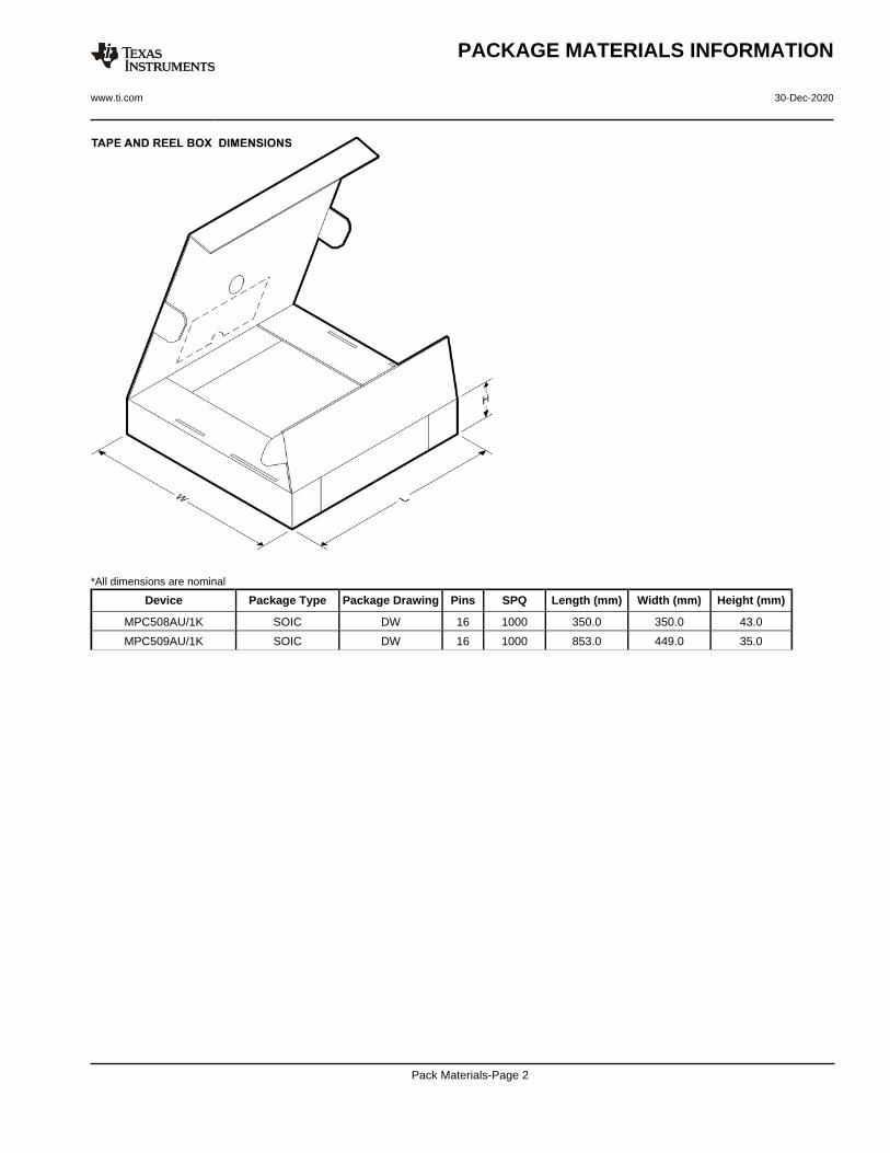
*All dimensions are nominal
Device Package Type Package Drawing Pins SPQ Length (mm) Width (mm) Height (mm)
MPC508AU/1K SOIC DW 16 1000 350.0 350.0 43.0
MPC509AU/1K SOIC DW 16 1000 853.0 449.0 35.0
PACKAGE MATERIALS INFORMATION
www.ti.com 30-Dec-2020
Pack Materials-Page 2
www.ti.com
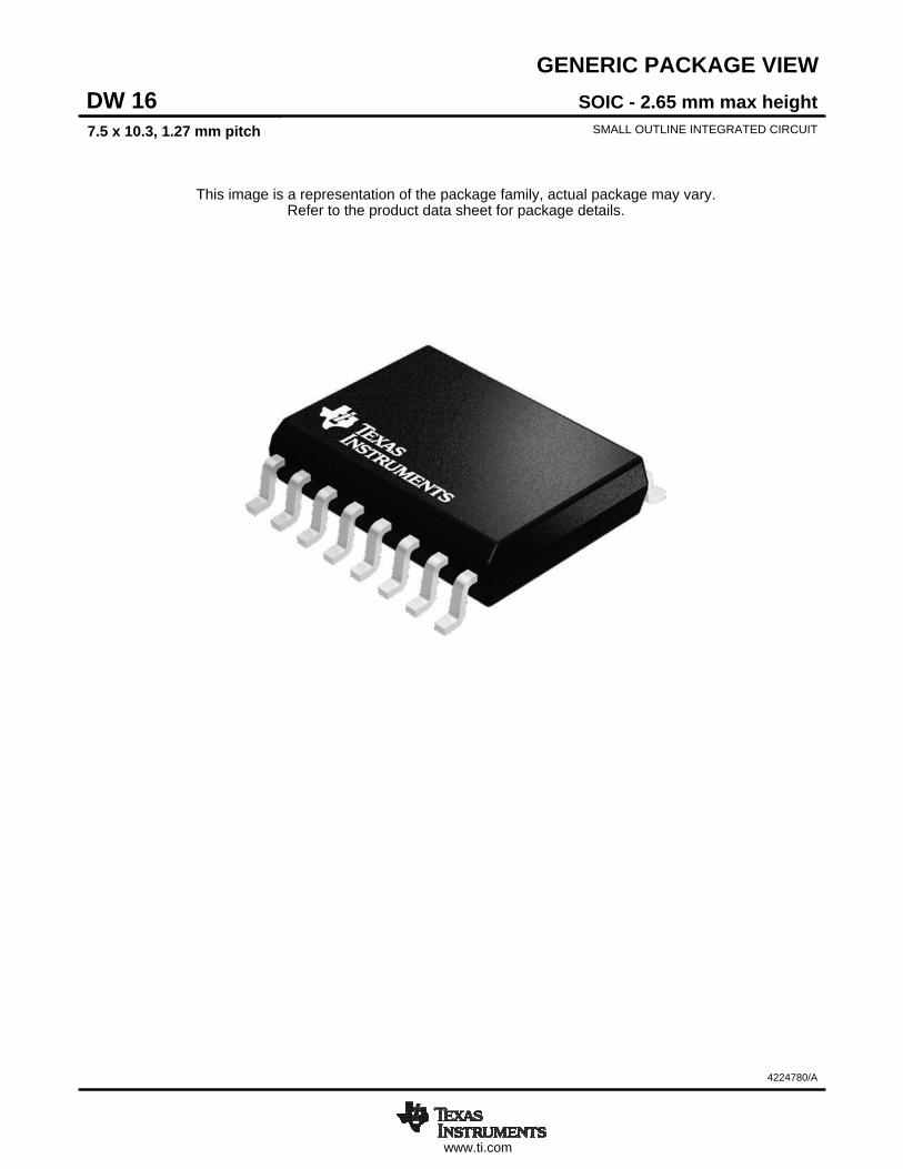
GENERIC PACKAGE VIEW
This image is a representation of the package family, actual package may vary.Refer to the product data sheet for package details.
SOIC - 2.65 mm max heightDW 16SMALL OUTLINE INTEGRATED CIRCUIT7.5 x 10.3, 1.27 mm pitch
4224780/A
www.ti.com
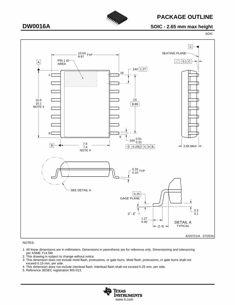
PACKAGE OUTLINE
C
TYP10.639.97
2.65 MAX
14X 1.27
16X 0.510.31
2X8.89
TYP0.330.10
0 - 80.30.1
(1.4)
0.25GAGE PLANE
1.270.40
A
NOTE 3
10.510.1
BNOTE 4
7.67.4
4220721/A 07/2016
SOIC - 2.65 mm max heightDW0016ASOIC
NOTES: 1. All linear dimensions are in millimeters. Dimensions in parenthesis are for reference only. Dimensioning and tolerancing per ASME Y14.5M. 2. This drawing is subject to change without notice. 3. This dimension does not include mold flash, protrusions, or gate burrs. Mold flash, protrusions, or gate burrs shall not exceed 0.15 mm, per side. 4. This dimension does not include interlead flash. Interlead flash shall not exceed 0.25 mm, per side.5. Reference JEDEC registration MS-013.
1 16
0.25 C A B
98
PIN 1 IDAREA
SEATING PLANE
0.1 C
SEE DETAIL A
DETAIL ATYPICAL
SCALE 1.500
www.ti.com
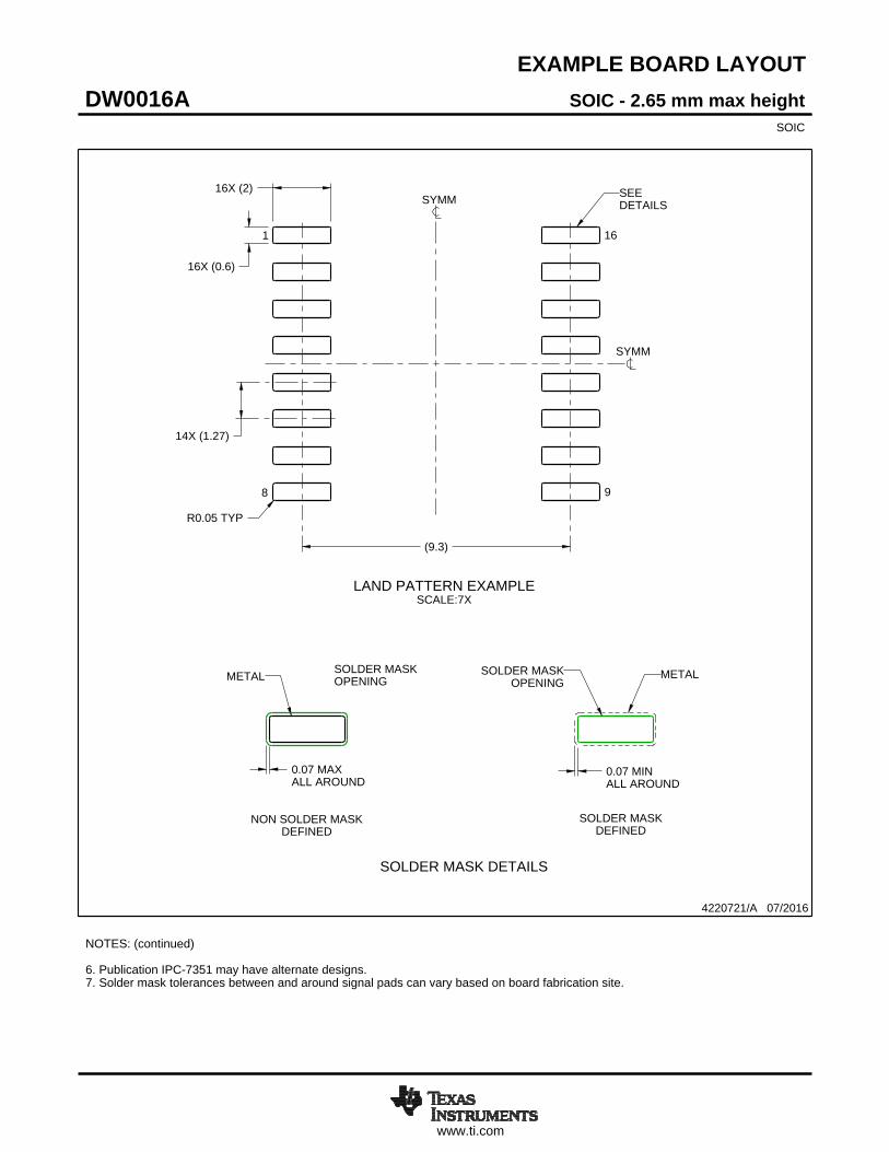
EXAMPLE BOARD LAYOUT
0.07 MAXALL AROUND
0.07 MINALL AROUND
(9.3)
14X (1.27)
R0.05 TYP
16X (2)
16X (0.6)
4220721/A 07/2016
SOIC - 2.65 mm max heightDW0016ASOIC
NOTES: (continued) 6. Publication IPC-7351 may have alternate designs. 7. Solder mask tolerances between and around signal pads can vary based on board fabrication site.
METAL SOLDER MASKOPENING
NON SOLDER MASKDEFINED
SOLDER MASK DETAILS
OPENINGSOLDER MASK METAL
SOLDER MASKDEFINED
LAND PATTERN EXAMPLESCALE:7X
SYMM
1
8 9
16
SEEDETAILS
SYMM
www.ti.com
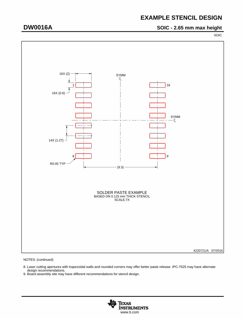
EXAMPLE STENCIL DESIGN
R0.05 TYP
16X (2)
16X (0.6)
14X (1.27)
(9.3)
4220721/A 07/2016
SOIC - 2.65 mm max heightDW0016ASOIC
NOTES: (continued) 8. Laser cutting apertures with trapezoidal walls and rounded corners may offer better paste release. IPC-7525 may have alternate design recommendations. 9. Board assembly site may have different recommendations for stencil design.
SOLDER PASTE EXAMPLEBASED ON 0.125 mm THICK STENCIL
SCALE:7X
SYMM
SYMM
1
8 9
16

IMPORTANT NOTICE AND DISCLAIMERTI PROVIDES TECHNICAL AND RELIABILITY DATA (INCLUDING DATASHEETS), DESIGN RESOURCES (INCLUDING REFERENCEDESIGNS), APPLICATION OR OTHER DESIGN ADVICE, WEB TOOLS, SAFETY INFORMATION, AND OTHER RESOURCES “AS IS”AND WITH ALL FAULTS, AND DISCLAIMS ALL WARRANTIES, EXPRESS AND IMPLIED, INCLUDING WITHOUT LIMITATION ANYIMPLIED WARRANTIES OF MERCHANTABILITY, FITNESS FOR A PARTICULAR PURPOSE OR NON-INFRINGEMENT OF THIRDPARTY INTELLECTUAL PROPERTY RIGHTS.These resources are intended for skilled developers designing with TI products. You are solely responsible for (1) selecting the appropriateTI products for your application, (2) designing, validating and testing your application, and (3) ensuring your application meets applicablestandards, and any other safety, security, or other requirements. These resources are subject to change without notice. TI grants youpermission to use these resources only for development of an application that uses the TI products described in the resource. Otherreproduction and display of these resources is prohibited. No license is granted to any other TI intellectual property right or to any third partyintellectual property right. TI disclaims responsibility for, and you will fully indemnify TI and its representatives against, any claims, damages,costs, losses, and liabilities arising out of your use of these resources.TI’s products are provided subject to TI’s Terms of Sale (https:www.ti.com/legal/termsofsale.html) or other applicable terms available eitheron ti.com or provided in conjunction with such TI products. TI’s provision of these resources does not expand or otherwise alter TI’sapplicable warranties or warranty disclaimers for TI products.IMPORTANT NOTICE
Mailing Address: Texas Instruments, Post Office Box 655303, Dallas, Texas 75265Copyright © 2021, Texas Instruments Incorporated