Embed Size (px)
Citation preview

Single molecule electronic devices with carbon-based materials:Status and opportunity
Downloaded from: https://research.chalmers.se, 2021-10-07 17:24 UTC
Citation for the original published paper (version of record):Ghasemi, S., Moth-Poulsen, K. (2021)Single molecule electronic devices with carbon-based materials: Status and opportunityNanoscale, 13(2): 659-671http://dx.doi.org/10.1039/d0nr07844a
N.B. When citing this work, cite the original published paper.
research.chalmers.se offers the possibility of retrieving research publications produced at Chalmers University of Technology.It covers all kind of research output: articles, dissertations, conference papers, reports etc. since 2004.research.chalmers.se is administrated and maintained by Chalmers Library
(article starts on next page)
Nanoscale
MINIREVIEW
Cite this: Nanoscale, 2021, 13, 659
Received 3rd November 2020,Accepted 18th December 2020
DOI: 10.1039/d0nr07844a
rsc.li/nanoscale
Single molecule electronic devices with carbon-based materials: status and opportunity
Shima Ghasemi and Kasper Moth-Poulsen *
The field of single molecule electronics has progressed remarkably in the past decades by allowing for
more versatile molecular functions and improving device fabrication techniques. In particular, electrodes
made from carbon-based materials such as graphene and carbon nanotubes (CNTs) may enable parallel
fabrication of multiple single molecule devices. In this perspective, we review the recent progress in the
field of single molecule electronics, with a focus on devices that utilizes carbon-based electrodes. The
paper is structured in three main sections: (i) controlling the molecule/graphene electrode interface using
covalent and non-covalent approaches, (ii) using CNTs as electrodes for fabricating single molecule
devices, and (iii) a discussion of possible future directions employing new or emerging 2D materials.
Introduction
Semiconductor technology is ubiquitous in our modern, con-nected society. In recent years, the use of on-line devicespowering the internet of things (IoT) has massively expanded.This transformation is powered by impressive developments inthe fabrication and miniaturization of silicon-based systems.Yet, to realize the rapid miniaturization trend as described byMoore’s law will likely require new technologies.1 These techno-logies should not only be quantum sized, but also consumelittle power, have a low environmental ramification and mustbe competitive in terms of cost. In this context, single-moleculeelectronics have been explored for several decades as one poss-ible avenue for electronic devices. For example, single moleculedevices with advanced functions such as switching,2–4
rectification,5,6 transistors7,8 and molecular diodes9 have beendeveloped. However, parallel fabrication and reproducibilityremain key issues for single-molecule electronic devices.
This could be resolved using carbon-based materials. Inparticular, graphene significantly reduces the number of poss-ible contact geometries and adds compelling electronic func-tions to single-molecule electronic devices. 2D materials maysoon also enable parallel fabrication of single-molecule elec-tronic devices for the first time. In this review, we highlightand discuss the status and opportunities of carbon-basedmaterials used in single-molecule electronics devices focusingon the progress in the recent 3–5 years (2016–2020). Thisreview concentrates on devices with a single or a smallnumber of active molecules. The broader field of electronic
devices based on self-assembled monolayers (SAMs) is notwithin the scope of this review.10–12,13
Molecule-electrode interface
When working with single molecule electronics devices, thegold coupled organic molecules with thiol based “alligatorclips” have been the preferred electrodes. However, the highatomic mobility and low chemical stability of metallic contactscould induce the destruction of molecular junctions upon oxi-dation or electromigration. Furthermore, small variations inthe positioning of a single molecule onto the electrode mayradically affect the electronic coupling between the moleculeand electrode. Further, the positioning of a gate close to themolecule in the metallic nanogap is difficult. These challengescould limit practical device function.14–17 Therefore, control-ling the fabrication of molecular junctions in the electrode–molecule interface has been challenging. Using electrodesmade of graphene could be a viable solution for the formationof reliable molecular junctions. Arrangement of sp2-hybridizedcarbon atoms in graphene provides the desired compatibilitywith organic molecules. The 2D structure of graphene reducesthe number of possible contact geometries compared to 3Dstructures, which potentially leads to a more reproduciblesingle molecule device. The binding of anchoring groups tographene electrodes can be achieved by either π–π interactionor covalent bonding. Anchoring groups play a crucial role forimproving the mechanical stability and electronic coupling ofthe molecule–electrode interface when they are attached to themolecular backbone. Other factors such as inserting spacersbetween the molecular backbone and anchoring groups couldoptimize the molecule–electrode interface efficiently. With this
Department of Chemistry and Chemical Engineering, Chalmers University of
Technology, SE-412-96 Göteborg, Sweden. E-mail: [email protected]
This journal is © The Royal Society of Chemistry 2021 Nanoscale, 2021, 13, 659–671 | 659
Ope
n A
cces
s A
rtic
le. P
ublis
hed
on 1
8 D
ecem
ber
2020
. Dow
nloa
ded
on 2
/9/2
021
12:4
0:20
PM
. T
his
artic
le is
lice
nsed
und
er a
Cre
ativ
e C
omm
ons
Attr
ibut
ion-
Non
Com
mer
cial
3.0
Unp
orte
d L
icen
ce.
View Article OnlineView Journal | View Issue
review, we present how different anchoring groups can controlcharge transport properties, switches and facilitate dynamicinvestigations based on the graphene–molecule–graphenesingle-molecule junctions (GMG-SMJs).
Non-covalent bonding betweenmolecule and graphene electrode
Interaction of different anchoring groups with electrodes candirectly influence the charge transport behavior of single-mole-cule devices. Any change of the molecular electrode interface,either electronically or geometrically could significantlychange the electrical conductance (G) of single molecules. Inorder to control the molecule–electrode interface through π–πstacking with a number of different anchoring groups (Fig. 1,structure a–i) has been investigated. In particular, El Abbassiet al. obtained a mechanically stable device by anchoring a smallnumber of molecules onto the SiO2 substrate between two gra-phene electrodes through a silanization reaction.18 The mole-cule was comprised of three main parts: a silane group, aπ-conjugated head group and a non-conjugated alkane chain(Fig. 2a). The silane group facilitated the chemical anchoringof the molecule to the substrate via covalent bonding. Thiscovalent anchoring of the molecule to the substrate overcamethe problem of ill-defined edge terminations in graphene thatcan occur after nanofabrication or preparation of the contactelectrodes. Additionally, covalent bonds between the moleculeand the substrate led to stable graphene–molecule junctions.The π-conjugated head group biphenyl N-carbazole (BPC;Fig. 1a) ensured coupling to graphene through π–π interaction.The non-conjugated alkane chain decoupled the mechanicalanchoring from the electronic head group. To reveal the trans-port characteristics at the molecule–electrode interface in thedevice, density functional theory (DFT) calculations have beenperformed. DFT analysis indicated that the frontier orbitals of
the BPC molecule were mostly localized on the head group.This shows that the electron transport occurs mainly throughthe head group. They also found the evidence for the for-mation of transport channels between the head groups of twoneighboring molecules through π–π stacking in the graphenenanogap (Fig. 2b). Apart from the BPC molecule, they did elec-trical characterization of devices with other headgroups, i.e.,molecule C with a carbazole (Fig. 1b) and molecule M withouta π-conjugated head group. Current–voltage (I–V) curvesshowed a maximum current of about 10 picoampere (pA) at abias voltage (Vb) of 2 V for the junction using molecule M. I–Vcurves for the junctions using molecule C illustrated efficientcharge transport over the molecular junction through π–πstacking. The alteration in I–V shapes and current levels wereexplained by the weak electronic interaction between the
Fig. 1 Examples of non-covalent anchoring groups used in graphene-based devices. (a) Biphenyl N-carbazole, (b) Carbazole, (c) Fullerene,(d) Pyrene, (e) Amine, (f ) Pyrene-1, (g) Pyrene-2, (h) Tetrabenzofluorene, (i) Anthracene.
Fig. 2 (a) Molecular structure. (b) Schematic of the molecular junctionincluding molecules bridged via different π–π-stacking into graphene.Reprinted with permission from El Abbassi et al., Nat. Nanotechnol.,2019, 14, 957. Copyright 2019 Nature Publishing Group.
Minireview Nanoscale
660 | Nanoscale, 2021, 13, 659–671 This journal is © The Royal Society of Chemistry 2021
Ope
n A
cces
s A
rtic
le. P
ublis
hed
on 1
8 D
ecem
ber
2020
. Dow
nloa
ded
on 2
/9/2
021
12:4
0:20
PM
. T
his
artic
le is
lice
nsed
und
er a
Cre
ativ
e C
omm
ons
Attr
ibut
ion-
Non
Com
mer
cial
3.0
Unp
orte
d L
icen
ce.
View Article Online
neighboring head groups, which were arranged in variousmolecular conformations.
Tan et al. realized a different approach for investigation ofcharge transport through a class of junctions using themechanically controlled break junction (MCBJ) technique.19
They fabricated single-fullerene (Fig. 1c) junctions with a full-erene bridged between two graphene electrodes via van derWaals interactions. A one-dimensional (1D) conductance histo-gram of graphene/single-C60, C70, C76, C90/graphene junctionsindicated that the conductance improved >250% from 2.0 ×10⁻⁵ G0 to 5.1 × 10⁻⁵ G0 when the size of the fullerene waschanged from C60 to C90. Furthermore, they observed that theconductance was enhanced after the fullerene was doped witha nitrogen atom. For example, the conductance of graphene/single-(C59N)2/graphene increased by 150% reaching 2.1 × 10⁻⁵
G0 compared to the conductance of graphene/single-C120/gra-phene junctions. However, when breaking the conjugation ofthe π-system of fullerene, the conductance decreased. The con-ductance of low-conjugated graphene/single-C50H10/graphenejunctions decreased by about one order of magnitude com-pared to the conductance of conjugated single-C60.
The charge transport in a series of C60-graphene junctionshas been investigated by Leitherer et al. using DFT andLandauer transport theory.20 As building blocks of the mole-cular junctions, they used a molecular bridge between two C60
molecules connected by two styrene groups covalently attachedto the [2,2] paracyclophane moiety in the center of C60. Thetwo fullerene anchor groups of this structure were bound tographene electrodes through π–π interaction.21 They found outtwo structural conformers with either zigzag- or armchair-ter-minated graphene nanocontacts (Fig. 3a and b) and investi-
gated how electronic transport is influenced by graphene edgeterminations. Interestingly, the edge-induced transport contri-butions were only observed in conformer A with zigzag-termi-nated graphene electrodes. This phenomenon was explainedby the differences in the interface geometry and the resultingmolecule–graphene contact in conformer A. As it is shown inFig. 3, for conformer B dimer/bridge and a hexagon hole geo-metry corresponded to the left- and right-hand side respect-ively. The binding energy of the hexagon/hole and pentagon/hole orientation, corresponded to conformer A, was higherthan that of the dimer/bridge geometry, which resultedthe lower molecule–electrode coupling in conformer B. Thedifferent coupling strengths in the pentagon and hexagon geo-metries was corroborated by earlier experimental work byDanilov et al.22 who studied voltage-induced switching insingle C60 molecules located in the nano gap between twosilver electrodes.
Limburg et al. explored five derivatives of zinc porphyrin insingle-molecule junctions to find out the effect of various non-covalent anchor groups on charge transport properties and thejunction formation probability (JFP).23 The five derivativeswere constituted of an identical redox-active zinc porphyrincore and different flat π-aromatic systems as anchor groups.They chose one reference molecule without anchor groups.Tetrabenzofluorene (Fig. 1h) anchors showed different chargetransport behaviour compared to the other anchors as they arenot π-conjugated with the porphyrin. The JFP is highlydepended on the anchor group. The larger anchor groups indi-cated higher binding energy which corresponded with higherJFPs of molecular devices. Specially, in this experiment, theyshowed that larger anchor groups had a significant positiveeffect on JFP. For example, 1,3,8-tridodecyloxypyrene and2,5,8,11,14-pentadodecylhexa-peri hexabenzocoronene had thehighest JFPs values of about 36% and 38%, respectively. Theyalso showed that additional alkyl tails on the π-systems playedthe role for better interaction of the π-system to the graphene.The large binding energies and high JFP of lager anchorgroups make them as a potential candidate for fabrication ofdevices based on molecular anchoring to graphene via π-stacking.
To investigate electron transport through spin-crossover(SCO) molecules at the single molecular level, Burzurí et al.bridged the molecule [Fe(L)2] (BF4)2·CH3CN·H2O (Fe-SCO)between two few-layer graphene (FLG) electrodes.24 The coordi-nation of two 2,6-bispyrazolylpyridine (bpp) ligands (L) with Fe(II) was through an octahedral (Oh) symmetry distorted to a S4symmetry. Two pyrene (Fig. 1d) groups anchored these ligandsvia π–π stacking to graphene electrodes. After deposition of theFe-SCO molecules, they calculated the current (I)–voltage (V)characteristics at cryogenic temperatures for three differentjunctions containing an Fe-SCO molecule. When a molecularjunction was formed, the current was increased sharplyaround two orders of magnitude compared with the emptyjunction. In these three junctions, they observed a reproduci-ble conductance bi-stability between a large-gap (LG) and asmall-gap (SG) state. This observation confirmed that the spin-crossover switch was active in these single-molecule junctions.
Fig. 3 Interface geometry of (a) conformer A and (b) conformerB. Reprinted with permission from Leitherer et al., Nanoscale, 2017, 9,7217. Copyright 2017 Royal Society of Chemistry.
Nanoscale Minireview
This journal is © The Royal Society of Chemistry 2021 Nanoscale, 2021, 13, 659–671 | 661
Ope
n A
cces
s A
rtic
le. P
ublis
hed
on 1
8 D
ecem
ber
2020
. Dow
nloa
ded
on 2
/9/2
021
12:4
0:20
PM
. T
his
artic
le is
lice
nsed
und
er a
Cre
ativ
e C
omm
ons
Attr
ibut
ion-
Non
Com
mer
cial
3.0
Unp
orte
d L
icen
ce.
View Article Online
DFT analysis indicated that the SCO transition induced a con-siderable change in the energy spectrum of the molecular orbi-tals led to conductance bistability. It has been shown thatsmall changes of the ligand distance in the molecular junc-tions could induce switching between high-spin (HS) and low-spin (LS) states at the single-molecule level at any temperature.Lau et al. studied the charge transport properties across a gra-phene–fullerene single-molecule transistor using a C60 bisad-duct functionalized with pyrene as an anchoring group. Twopyrene anchor groups were bound to graphene nanoelectrodesvia π–π interactions.25 DFT calculations revealed that the moststable configuration was the cis-3 isomer of relaxed graphene–fullerene–graphene structure without steric hindrance. Theiso-surfaces of the frontier orbitals for cis-3 and cis-2 indicatedthat the cis-3 isomer showed better π–π interaction with thegraphene electrodes. It should be noted that the transport inpristine C60 was dominated by the lowest unoccupied mole-cular orbital (LUMO), whereas functionalization of C60 withpyrene anchoring groups modified the electron delocalizationand energy levels, which led to transport dominated by thehighest occupied molecular orbital (HOMO). Due to the stabi-lity of the device which showed weak vibron-relaxation, theyinvestigated redox-dependent electron–vibron coupling andavalanche transport.
To identify the influence of different anchoring groups onthe transport through graphene-based molecular junctions,Sadeghi et al. theoretically determined the electronic pro-perties of zinc-porphyrin monomers, dimers, and trimersattached to graphene electrodes through either π–π or covalentanchoring.26 The authors’ model device structure was com-prised of monomer, dimer and, trimer zinc-porphyrin wirescoupled to graphene electrodes (Fig. 4a) through eithercovalent C–C bond attachment to the edge of the grapheneribbons (Fig. 4b), amine anchors (Fig. 4c), π–π stackingthrough pyrene with two different moieties (Fig. 4d and e) or atetrabenzofluorene (TBF) anchoring group (Fig. 4f). Direct C–Ccoupling was found to have the highest conductance, followedby π–π stacking with the pyrene anchors, direct coupling viaamine anchors, and π–π stacking with TBF. The direct C–Cbonds were coupled to the electrodes more strongly than otheranchoring groups because of the great width of the HOMOresonance in this junction.27 Depending on the connectivity ofthe pyrene anchor groups to the porphyrin wire, pyreneanchors could induce either destructive quantum interferenceor different degrees of constructive quantum interference.However, the coupling of TBF to both the graphene and theporphyrin wires were weak as the twisted structure of the TBFanchors provided a nonuniform π–π overlap between π-orbitalsof TBF and the graphene electrodes. Furthermore, the disturb-ance in the conjugation of the π-aromatic system at the cyclo-pentadiene connection point led to a reduction in the conduc-tance and electronic coupling. The lower conductance ofamine anchors was explained by presence of a carbonyl group,which broke the conjugation of the π-aromatic system.
Prins et al. developed a method for the formation of nano-meter-separated FLG electrodes by using the feedback-con-
trolled electroburning technique.28 The high stability of theseelectrodes was demonstrated by only small variations in thetunneling characteristics after several weeks of storage undervacuum condition. In order to show the long-term stabilityand gate independent transport across the gap, an anthracene-functionalized curcuminoid molecule (1,7-(di-9-anthracene)-1,6-heptadiene-3,5-dione, 9Accm) was placed in the graphenenanogap. The anthracene groups (Fig. 1i) interacted via π–πinteractions with the FLG electrodes and the high π-electrondensity of 9 Accm facilitated the charge transport. The differ-ence in I–V characteristics before and after molecule depo-sition could be explained by the presence of molecules in thegap influencing its stability. Before deposition, the conduc-tance was gate-independent and after deposition, the conduc-tance of the device improved and gate-dependent transport atroom temperature was observed, indicative of molecular deviceformation.
A more reproducible electrode–molecule contact than fortraditional anchoring groups covalently binding to the metalelectrode has been achieved by designing a new curcuminoid-based molecule (9ALCccmoid) with a well-defined geometry ofaromatic anchoring groups such as pyrene and anthracene.29
9ALCccmoid was comprised of a conjugated linear chain of 11C atoms which included a β-diketone group at the center ofthe backbone and two anthracene groups situated on bothsides of the chain. The molecule–electrode interface was con-trolled by π–π stacking of the anthracene groups to the FLGelectrodes. I–V curves revealed that the current was reducedduring controlled electroburning of a typical device ineach step. Modelling of the structure indicated that the
Fig. 4 (a) The porphyrin wires with one, two, and three zinc porphyrinunits (n = 1, 2, 3) are contacted to the graphene by pyrene anchors.Other anchor groups studied include covalent anchoring to the edge ofgraphene electrodes via (b) a direct carbon–carbon bond and (c) amineanchors or through π–π interactions with (d) pyrene-1 anchors, (e)pyrene-2 anchors, and (f ) tetrabenzofluorene (TBF) anchors. Reprintedwith permission from Sadeghi et al., Nano Lett., 2017, 17, 4611. Copyright2017 American Chemical Society.
Minireview Nanoscale
662 | Nanoscale, 2021, 13, 659–671 This journal is © The Royal Society of Chemistry 2021
Ope
n A
cces
s A
rtic
le. P
ublis
hed
on 1
8 D
ecem
ber
2020
. Dow
nloa
ded
on 2
/9/2
021
12:4
0:20
PM
. T
his
artic
le is
lice
nsed
und
er a
Cre
ativ
e C
omm
ons
Attr
ibut
ion-
Non
Com
mer
cial
3.0
Unp
orte
d L
icen
ce.
View Article Online
9ALCccmoid molecule was positioned on top of the vicinity ofeach graphene electrode with one anthracene group. An energyminimum observed with a negligible relative horizontal shiftof the graphene electrodes could be the reason for the non-symmetric final structure.
The charge transport through a stable single-moleculesingle-electron transistor (SET) was investigated by Mol et al.30
They used a molecular backbone of a zinc-porphyrin moietyconnecting to ‘butterfly’ TBF anchoring groups with a spacer,which facilitated the binding via π–π-stacking to defect freegraphene nano-electrodes. DFT analysis revealed no sign ofsteric hindrance to adsorption as well as a planar geometry ofthe molecular wire across the graphene nanogap. A wide rangeof molecular wires can possibly be used for the π–π anchoringto the highly stable graphene electrodes.
Covalent bonding between moleculeand graphene electrodes
Apart from studying the charge transport properties withinsingle molecule electronics, there are several reports usingGMG-SMJ platform for investigation of dynamic processes atthe single-molecule level such as host–guest interactions,hydrogen bond interactions, and intermolecular chemicalreactions. In these studies, they controlled the molecule–elec-trode interface by covalent coupling of a wide range of organicmolecules have been used with graphene electrodes.
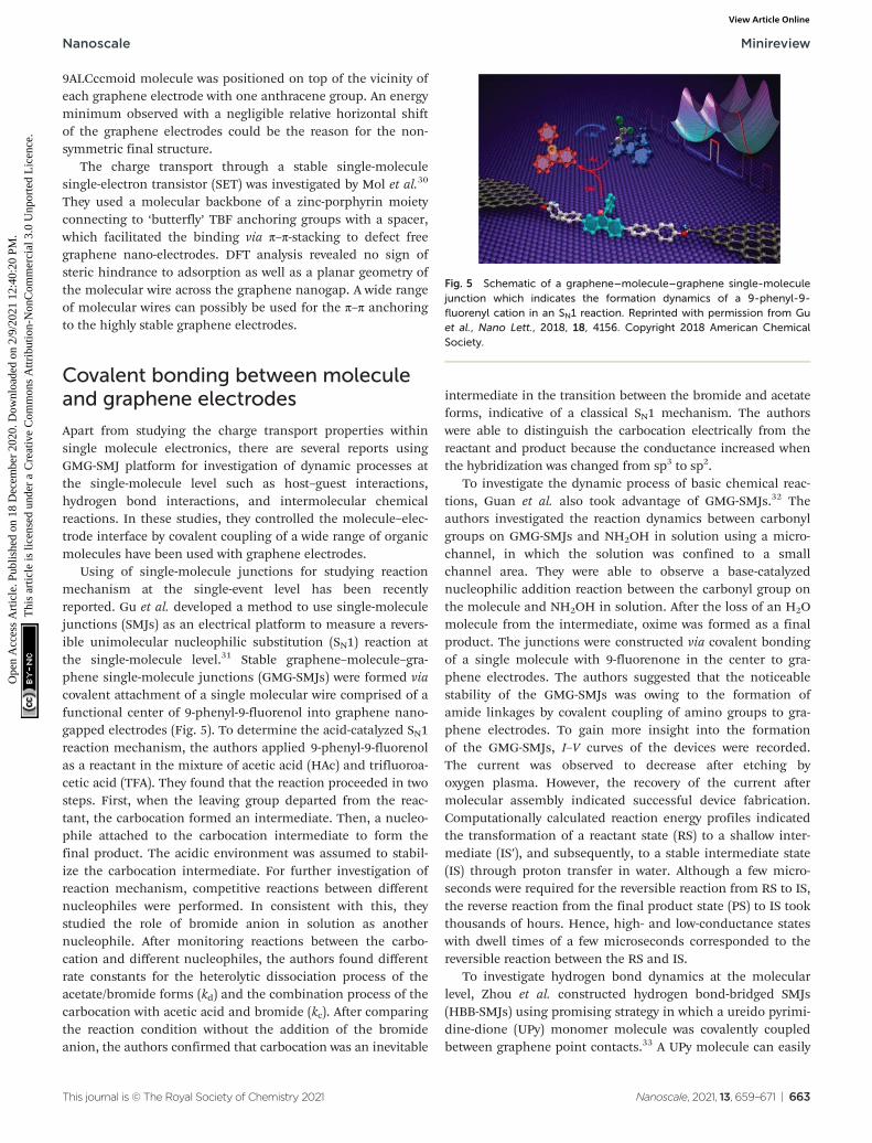
Using of single-molecule junctions for studying reactionmechanism at the single-event level has been recentlyreported. Gu et al. developed a method to use single-moleculejunctions (SMJs) as an electrical platform to measure a revers-ible unimolecular nucleophilic substitution (SN1) reaction atthe single-molecule level.31 Stable graphene–molecule–gra-phene single-molecule junctions (GMG-SMJs) were formed viacovalent attachment of a single molecular wire comprised of afunctional center of 9-phenyl-9-fluorenol into graphene nano-gapped electrodes (Fig. 5). To determine the acid-catalyzed SN1reaction mechanism, the authors applied 9-phenyl-9-fluorenolas a reactant in the mixture of acetic acid (HAc) and trifluoroa-cetic acid (TFA). They found that the reaction proceeded in twosteps. First, when the leaving group departed from the reac-tant, the carbocation formed an intermediate. Then, a nucleo-phile attached to the carbocation intermediate to form thefinal product. The acidic environment was assumed to stabil-ize the carbocation intermediate. For further investigation ofreaction mechanism, competitive reactions between differentnucleophiles were performed. In consistent with this, theystudied the role of bromide anion in solution as anothernucleophile. After monitoring reactions between the carbo-cation and different nucleophiles, the authors found differentrate constants for the heterolytic dissociation process of theacetate/bromide forms (kd) and the combination process of thecarbocation with acetic acid and bromide (kc). After comparingthe reaction condition without the addition of the bromideanion, the authors confirmed that carbocation was an inevitable
intermediate in the transition between the bromide and acetateforms, indicative of a classical SN1 mechanism. The authorswere able to distinguish the carbocation electrically from thereactant and product because the conductance increased whenthe hybridization was changed from sp3 to sp2.
To investigate the dynamic process of basic chemical reac-tions, Guan et al. also took advantage of GMG-SMJs.32 Theauthors investigated the reaction dynamics between carbonylgroups on GMG-SMJs and NH2OH in solution using a micro-channel, in which the solution was confined to a smallchannel area. They were able to observe a base-catalyzednucleophilic addition reaction between the carbonyl group onthe molecule and NH2OH in solution. After the loss of an H2Omolecule from the intermediate, oxime was formed as a finalproduct. The junctions were constructed via covalent bondingof a single molecule with 9-fluorenone in the center to gra-phene electrodes. The authors suggested that the noticeablestability of the GMG-SMJs was owing to the formation ofamide linkages by covalent coupling of amino groups to gra-phene electrodes. To gain more insight into the formationof the GMG-SMJs, I–V curves of the devices were recorded.The current was observed to decrease after etching byoxygen plasma. However, the recovery of the current aftermolecular assembly indicated successful device fabrication.Computationally calculated reaction energy profiles indicatedthe transformation of a reactant state (RS) to a shallow inter-mediate (IS′), and subsequently, to a stable intermediate state(IS) through proton transfer in water. Although a few micro-seconds were required for the reversible reaction from RS to IS,the reverse reaction from the final product state (PS) to IS tookthousands of hours. Hence, high- and low-conductance stateswith dwell times of a few microseconds corresponded to thereversible reaction between the RS and IS.
To investigate hydrogen bond dynamics at the molecularlevel, Zhou et al. constructed hydrogen bond-bridged SMJs(HBB-SMJs) using promising strategy in which a ureido pyrimi-dine-dione (UPy) monomer molecule was covalently coupledbetween graphene point contacts.33 A UPy molecule can easily
Fig. 5 Schematic of a graphene–molecule–graphene single-moleculejunction which indicates the formation dynamics of a 9-phenyl-9-fluorenyl cation in an SN1 reaction. Reprinted with permission from Guet al., Nano Lett., 2018, 18, 4156. Copyright 2018 American ChemicalSociety.
Nanoscale Minireview
This journal is © The Royal Society of Chemistry 2021 Nanoscale, 2021, 13, 659–671 | 663
Ope
n A
cces
s A
rtic
le. P
ublis
hed
on 1
8 D
ecem
ber
2020
. Dow
nloa
ded
on 2
/9/2
021
12:4
0:20
PM
. T
his
artic
le is
lice
nsed
und
er a
Cre
ativ
e C
omm
ons
Attr
ibut
ion-
Non
Com
mer
cial
3.0
Unp
orte
d L
icen
ce.
View Article Online
dimerize in a weak polar solvent such as diphenyl ether. Inthis study, A UPy dimer played the role as a good conductingchannel and facilitated the formation of a strong donor–donor–acceptor–acceptor array of intermolecular quadruplehydrogen bonding. However, changing to strong polar solventssuch as water, diphenyl ether could lead to on–off switching ofthe conductance of HBB-SMJs. This result indicated the suc-cessful fabrication of the devices. After studying the obtainedcurrent–time (I–t ) curves in 1,1,2,2-tetrachloroethane (TeCA) at293 K, they observed a series of large-amplitude two-state fluc-tuations with considerable dependency to temperature andsolvent dependence. It has been shown that compared to the‘high’ state conductance, the conductance of the ‘low’ statewas much smaller which indicated a weaker hydrogenbonding system. The average lifetimes for the high-conduc-tance and low-conductance states were reported τhigh = ∼0.660± 0.042 ms and τlow = ∼0.581 ± 0.042 ms respectively. In orderto clarify the dynamic mechanism, they studied the experi-ments in two solvents with three different temperatures. Theyobserved two large-amplitude peaks in TeCA. However, a multi-modal distribution (at least four obvious peaks) was detectedin diphenyl ether suggesting different mechanisms of inter-molecular interactions through hydrogen bonding in differentsolvents. Both experimental and theoretical results revealedthat a multimodal distribution could arise from the stochasticrearrangement of the hydrogen bond structure mainly throughintermolecular proton transfer and lactam–lactim tautomer-ism. This work shows a promising strategy for investigation ofhydrogen bond dynamics at the single molecule level.
To study the capability of particular GMG-SMJs to discoverthermodynamic and kinetic parameters of a host–guestcomplex, Wen et al. constructed a conjugated molecular wirefeaturing bis-p-phenylene [34] crown-10 (BPP34C10) termi-nated with two amine handles namely, BPP34C10DAMthat was covalently attached to carboxylic acid–terminatedgraphene point contacts using a 1-ethyl-3-(3-dimethyl-aminopropyl)carbodiimide (EDCI) coupling protocol.34 Withthis interface, they were able to transduce the physical pseu-dorotaxane (de)formation processes between the electron-richcrown ether and a dicationic guest into real-time electricalsignals. To gain more insight to the influence of host–guestinteractions on the conductivity of molecular junctions, theystarted the complexation by introducing methyl viologen(MV2+), which widely used as a guest for the BPP34C10 host,into the GMG-SMJ system. After immersion in a Me2SO solu-tion containing 1 mM MV·2PF6 for 12 hours. The I–t curves ofresulting devices (MV2+ ⊂ BPP34C10-SMJs) indicated two dis-tinct “high” and “low” states. With the knowledge of a changein conductance in the solid state after MV2+ addition, the highand low conductance sates could be attributed to the associ-ation and dissociation processes between the BPP34C10 hostand MV2+ guest molecules at the device-liquid interface. Forfurther investigation, they calculated the transmissionspectra of both the BPP34C10 host and the MV2+ ⊂BPP34C10 pseudorotaxane in the SMJ by using an equilibriumGreen’s function technique based on DFT. The theoretical
result confirmed that electron (LUMO) transport was predomi-nant for both BPP34C10 and the MV2+ ⊂ BPP34C10 complex inthe graphene-based system. However, the LUMO of the MV2+ ⊂BPP34C10 pseudorotaxane SMJ was more delocalized, indica-tive of a better conductive channel. This study can provide thisopportunity for investigation of stochastic and dynamic natureof molecular recognition processes in both chemical and bio-logical system.
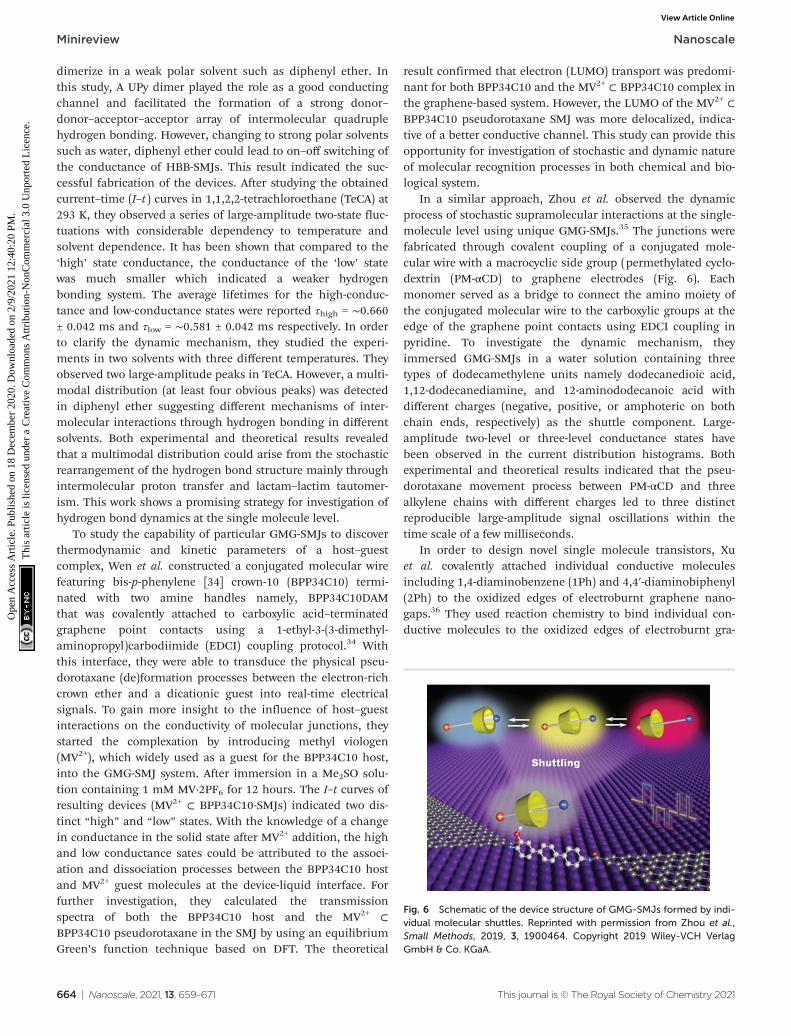
In a similar approach, Zhou et al. observed the dynamicprocess of stochastic supramolecular interactions at the single-molecule level using unique GMG-SMJs.35 The junctions werefabricated through covalent coupling of a conjugated mole-cular wire with a macrocyclic side group (permethylated cyclo-dextrin (PM-αCD) to graphene electrodes (Fig. 6). Eachmonomer served as a bridge to connect the amino moiety ofthe conjugated molecular wire to the carboxylic groups at theedge of the graphene point contacts using EDCI coupling inpyridine. To investigate the dynamic mechanism, theyimmersed GMG-SMJs in a water solution containing threetypes of dodecamethylene units namely dodecanedioic acid,1,12-dodecanediamine, and 12-aminododecanoic acid withdifferent charges (negative, positive, or amphoteric on bothchain ends, respectively) as the shuttle component. Large-amplitude two-level or three-level conductance states havebeen observed in the current distribution histograms. Bothexperimental and theoretical results indicated that the pseu-dorotaxane movement process between PM-αCD and threealkylene chains with different charges led to three distinctreproducible large-amplitude signal oscillations within thetime scale of a few milliseconds.
In order to design novel single molecule transistors, Xuet al. covalently attached individual conductive moleculesincluding 1,4-diaminobenzene (1Ph) and 4,4′-diaminobiphenyl(2Ph) to the oxidized edges of electroburnt graphene nano-gaps.36 They used reaction chemistry to bind individual con-ductive molecules to the oxidized edges of electroburnt gra-
Fig. 6 Schematic of the device structure of GMG-SMJs formed by indi-vidual molecular shuttles. Reprinted with permission from Zhou et al.,Small Methods, 2019, 3, 1900464. Copyright 2019 Wiley-VCH VerlagGmbH & Co. KGaA.
Minireview Nanoscale
664 | Nanoscale, 2021, 13, 659–671 This journal is © The Royal Society of Chemistry 2021
Ope
n A
cces
s A
rtic
le. P
ublis
hed
on 1
8 D
ecem
ber
2020
. Dow
nloa
ded
on 2
/9/2
021
12:4
0:20
PM
. T
his
artic
le is
lice
nsed
und
er a
Cre
ativ
e C
omm
ons
Attr
ibut
ion-
Non
Com
mer
cial
3.0
Unp
orte
d L
icen
ce.
View Article Online
phene nanogaps. The shape and size of the graphene nano-gaps provided a pathway to optimize the coupling chemistry.This led to high connection yields with ultrashort covalentsingle-molecule bridges (up to 40%). Therefore, extremelyshort molecules (as short as 0.6 nm in length) could find a wayto connect into the electrical circuit chemically. The reconnec-tion was observed after increasing the conductance across thenanogap using gate-dependent single-electron tunnelling pro-perties. They realized that the nature of the molecule influ-enced the yield of reconnection.
An approach by Xin et al. presents a new avenue for engin-eering high-performance electronic devices based onGMG-SMJs with an ionic liquid as a gate dielectric modulatingthe charge transport efficiently.37 To gain more insight intothe effectiveness of ionic liquid gating, three different phenyl-based molecular structures with various molecular lengthsincluding biphenyl, triphenyl and hexaphenyl molecules werecovalently coupled to graphene electrodes through amide lin-kages (Fig. 7). The conductance of the single-molecule junc-tions decreased when the length of the molecular backbonewas increased. These three devices indicated gate-controlledconductance behaviour. It has been shown that the molecularlength influenced the gate efficiency. When the gate voltagewas changed from −1.5 V to 1.5 V, both triphenyl and hexaphe-nyl molecular junctions showed ambipolar charge transportcharacteristics. This phenomenon explained by changing of
the dominant conducting orbital from HOMO to LUMO whenthe gate voltage was changed from negative to positive.
Sun et al.38 fabricated reliable junctions through a chemicalreaction between the amino-terminated hexaphenyl aromaticmolecule 4,4′-diaminohexaphenyl (DAHP) and the carboxylgroups at the edges of single-layer graphene nanoelectrodes.Hexaphenyl molecules are covalently linked to the grapheneelectrodes through amide linkages. They recorded I–V curvesof graphene–hexaphenyl–graphene (GHG) junctions at variouspoints after fabrication. The I–V curves before and after DAHPmolecule connection were compared. When one or few mole-cules have been interlinked the nano-gaps, a distinct currentincrease was observed. In order to determine of stability ofsingle-molecule devices, they recorded I–V curves of the samegraphene–hexaphenyl–graphene (GHG) junctions at variouspoints after fabrication. The authors did not observe anyremarkable changes in the I–V curves of the GHG junctionsmeasured immediately after fabrication, and two and fourweeks after fabrication. It has been shown that more than 52%of the devices could remain stable for up to four weeks atroom temperature.
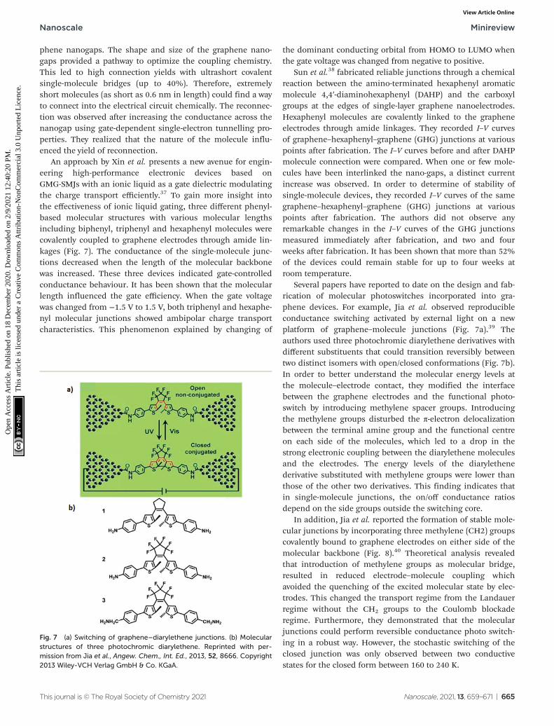
Several papers have reported to date on the design and fab-rication of molecular photoswitches incorporated into gra-phene devices. For example, Jia et al. observed reproducibleconductance switching activated by external light on a newplatform of graphene–molecule junctions (Fig. 7a).39 Theauthors used three photochromic diarylethene derivatives withdifferent substituents that could transition reversibly betweentwo distinct isomers with open/closed conformations (Fig. 7b).In order to better understand the molecular energy levels atthe molecule–electrode contact, they modified the interfacebetween the graphene electrodes and the functional photo-switch by introducing methylene spacer groups. Introducingthe methylene groups disturbed the π-electron delocalizationbetween the terminal amine group and the functional centreon each side of the molecules, which led to a drop in thestrong electronic coupling between the diarylethene moleculesand the electrodes. The energy levels of the diarylethenederivative substituted with methylene groups were lower thanthose of the other two derivatives. This finding indicates thatin single-molecule junctions, the on/off conductance ratiosdepend on the side groups outside the switching core.
In addition, Jia et al. reported the formation of stable mole-cular junctions by incorporating three methylene (CH2) groupscovalently bound to graphene electrodes on either side of themolecular backbone (Fig. 8).40 Theoretical analysis revealedthat introduction of methylene groups as molecular bridge,resulted in reduced electrode–molecule coupling whichavoided the quenching of the excited molecular state by elec-trodes. This changed the transport regime from the Landauerregime without the CH2 groups to the Coulomb blockaderegime. Furthermore, they demonstrated that the molecularjunctions could perform reversible conductance photo switch-ing in a robust way. However, the stochastic switching of theclosed junction was only observed between two conductivestates for the closed form between 160 to 240 K.
Fig. 7 (a) Switching of graphene–diarylethene junctions. (b) Molecularstructures of three photochromic diarylethene. Reprinted with per-mission from Jia et al., Angew. Chem., Int. Ed., 2013, 52, 8666. Copyright2013 Wiley-VCH Verlag GmbH & Co. KGaA.
Nanoscale Minireview
This journal is © The Royal Society of Chemistry 2021 Nanoscale, 2021, 13, 659–671 | 665
Ope
n A
cces
s A
rtic
le. P
ublis
hed
on 1
8 D
ecem
ber
2020
. Dow
nloa
ded
on 2
/9/2
021
12:4
0:20
PM
. T
his
artic
le is
lice
nsed
und
er a
Cre
ativ
e C
omm
ons
Attr
ibut
ion-
Non
Com
mer
cial
3.0
Unp
orte
d L
icen
ce.
View Article Online
A different type of photoswitch based on a GMG-SMJ wasintroduced by Meng et al. using an azobenzene derivative, acommon photochromic material with two states (cis/trans).41
Individual 2′-p-tolyldiazenyl-1,1′:4,4′-terphenyl-4,4″-dicar-boxylic acid (TTDA) molecules, were covalently attached to gra-phene electrodes through amide bond formation. Both the cisand trans forms of the azobenzene unit affected the electronicstructure of the whole molecule. Isomerization between thestates could be induced under irradiation of different wave-lengths of light (UV/visible) causing different resistancedisplay by different isomers. Both theoretical and experimentalanalysis confirmed that an electric field could modulate notonly the energy difference between the trans and cis forms, butalso the energy barrier of conformational changes.
Wu et al. theoretically determined the switching propertiesin a class of porphyrin molecules with pendant dipoles.42
Device fabrication involved covalent coupling of porphyrin tographene electrodes. The porphyrin moiety was gated by athird electrode. This study revealed that by altering thenumber of C–C triple bonds (used as spacer units between por-phyrin and graphene) from one to four, the room temperatureon/off conductance ratio changed from 100 to 200. Whenthe temperature was reduced to 100 K, this switching ratioenhanced approximately to 2200. These findings indicate thatporphyrin molecular junctions can be tuned systematically byadjusting the number of spacer units.
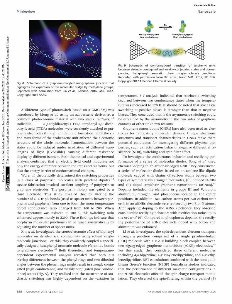
Xin et al. investigated the stereoelectronic effect of biphenylmolecules on its electrical conductivity using robust single-molecule junctions. For this, they covalently coupled a specifi-cally designed hexaphenyl aromatic molecule via amide bondsto graphene electrodes.43 Both theoretical and temperature-dependent experimental analysis revealed that both π–πoverlap differences between the phenyl rings and two dihedralangles between the phenyl rings might result in strongly conju-gated (high conductance) and weakly conjugated (low conduc-tance) states (Fig. 9). They realized that the occurrence of sto-chastic switching was highly dependent on the variation in
temperature. I–V analysis indicated that stochastic switchingoccurred between two conductance states when the tempera-ture was increased to 120 K. It should be noted that stochasticswitching at positive biases is stronger than that at negativebiases. They concluded that is the asymmetric switching couldbe explained by the asymmetry in the two sides of graphenecontacts or other unknown reasons.
Graphene nanoribbons (GNRs) have also been used as elec-trodes for fabricating molecular devices. Unique electronicstructures and transport characteristics in GNRs make thempotential candidates for investigating different physical pro-perties, such as rectification behavior negative differential re-sistance (NDR), switching and spin filter effect.
To investigate the conductance behavior and rectifying per-formance of a series of molecular diodes, Song et al. usedchemical doping in an armchair edged GNR. They constructeda series of molecular diodes based on an azulene-like dipolemolecule capped with chains of carbon atoms between twotypes of symmetrically arranged electrodes, (i) undoped zGNRsand (ii) doped armchair graphene nanoribbons (aGNRs).44
Dopants included the elements in groups III and V, boron,aluminum, nitrogen, and phosphorus located in the centerpositions. In addition, two carbon atoms per two carbon unitcells in an aGNRs electrode were replaced by two B or N atoms.After applying doping to the aGNR electrodes, they observedconsiderable rectifying behaviors with rectification ratios up tothe order of 105. Compared to phosphorus dopants, the rectify-ing performance of aGNR electrode doped with boron andaluminum was enhanced.
Li et al. investigated the spin-dependent electron transportthrough a junction comprised of a single pyridine-linked(PDL) molecule with a π–σ–π building block coupled betweentwo zigzag-edged graphene nanoribbon (zGNR) electrodes.45
For this study, they considered three different moleculesincluding 4,4-bipyridine, 4,4′-vinylenedipyridine, and 4,4′-ethy-lenedipyridine. DFT calculations combined with the nonequili-brium Green’s function (NEGF) formalism studies indicatedthat the performance of different magnetic configurations inthe zGNR electrodes affected the spin-charge transport modu-lation. They observed the spin-filtering within the parallel (P)
Fig. 8 Schematic of a graphene-diarylethene-graphene junction thathighlights the expansion of the molecular bridge by methylene groups.Reprinted with permission from Jia et al., Science, 2016, 352, 1443.Copy right 2016 AAAS.
Fig. 9 Schematic of conformational transition of terphenyl unitsbetween strongly conjugated and weakly-conjugated states and corres-ponding hexaphenyl aromatic chain single-molecule junctions.Reprinted with permission from Xin et al., Nano Lett., 2017, 17, 856.Copyright 2017 American Chemical Society.
Minireview Nanoscale
666 | Nanoscale, 2021, 13, 659–671 This journal is © The Royal Society of Chemistry 2021
Ope
n A
cces
s A
rtic
le. P
ublis
hed
on 1
8 D
ecem
ber
2020
. Dow
nloa
ded
on 2
/9/2
021
12:4
0:20
PM
. T
his
artic
le is
lice
nsed
und
er a
Cre
ativ
e C
omm
ons
Attr
ibut
ion-
Non
Com
mer
cial
3.0
Unp
orte
d L
icen
ce.
View Article Online
spin configuration and dual spin-filtering effect with antiparal-lel (AP) spin configuration. It is worth noting that for the junc-tions including a 4,4′-bipyridine molecule, the rectificationratio (RR) and the NDR effect with peak to valley ratio (PVR)could reach up to 104 and 328, respectively.
Wang et al. investigated the influence of intramolecularproton transfer on the current of single-molecule devicesbased on keto and enol tautomers.46 They used 6,11-dioxo-5,6,11,12 tetrahydrobenzo[b]phenazine- 1,4,7,10-tetracarboni-trile (DO-THBbPA-TCN) molecule attached covalently betweentwo zigzag graphene nanoribbon (zGNR) electrodes (Fig. 10).47
The interconversion between the keto and enol forms occurredthrough intermolecular proton transfer. They found that com-pared to keto molecular devices, the switching effect wasenhanced for the enol molecular device with an on/off ratio ofup to 3.4 × 10².
To understand bidirectional conductance switching, Hanet al. theoretically studied the molecule–electrode interface ofreversible molecular photoswitches based on diarylethenemolecules.48 The molecular junctions were designed and builtbased on the ring-closed and ring-open forms of diarylethenemolecules that were sandwiched between two monolayer gra-phene nanoribbons (GNRs) and two Au (111) electrodes. Thephotoswitching circle of the open and closed isomers was acti-vated in both directions using irradiation with visible light.They found that the electrical conductivity and switching be-havior depends on the electronic structure of molecule in boththe GNRs and Au electrode. Theoretical predications indicatedthat the on/off current ratio of the devices could be as largeas 103.
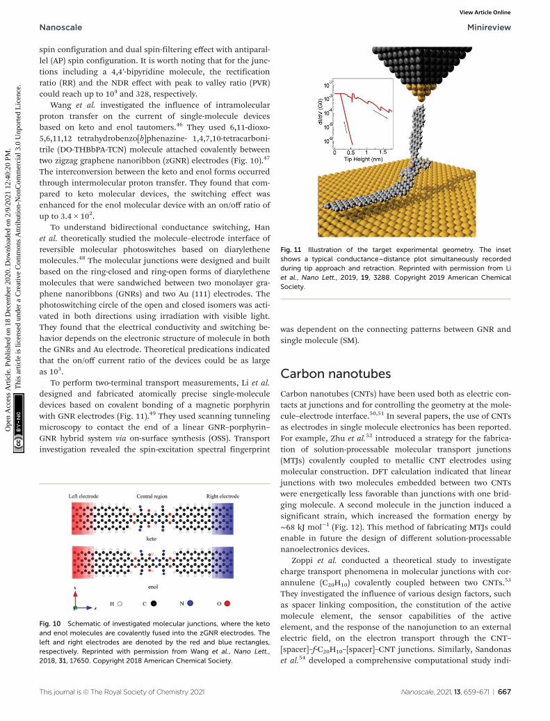
To perform two-terminal transport measurements, Li et al.designed and fabricated atomically precise single-moleculedevices based on covalent bonding of a magnetic porphyrinwith GNR electrodes (Fig. 11).49 They used scanning tunnelingmicroscopy to contact the end of a linear GNR–porphyrin–GNR hybrid system via on-surface synthesis (OSS). Transportinvestigation revealed the spin-excitation spectral fingerprint
was dependent on the connecting patterns between GNR andsingle molecule (SM).
Carbon nanotubes
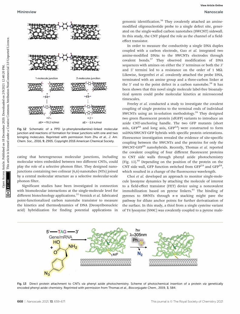
Carbon nanotubes (CNTs) have been used both as electric con-tacts at junctions and for controlling the geometry at the mole-cule–electrode interface.50,51 In several papers, the use of CNTsas electrodes in single molecule electronics has been reported.For example, Zhu et al.52 introduced a strategy for the fabrica-tion of solution-processable molecular transport junctions(MTJs) covalently coupled to metallic CNT electrodes usingmolecular construction. DFT calculation indicated that linearjunctions with two molecules embedded between two CNTswere energetically less favorable than junctions with one brid-ging molecule. A second molecule in the junction induced asignificant strain, which increased the formation energy by∼68 kJ mol−1 (Fig. 12). This method of fabricating MTJs couldenable in future the design of different solution-processablenanoelectronics devices.
Zoppi et al. conducted a theoretical study to investigatecharge transport phenomena in molecular junctions with cor-annulene (C20H10) covalently coupled between two CNTs.53
They investigated the influence of various design factors, suchas spacer linking composition, the constitution of the activemolecule element, the sensor capabilities of the activeelement, and the response of the nanojunction to an externalelectric field, on the electron transport through the CNT–[spacer]–f-C20H10–[spacer]–CNT junctions. Similarly, Sandonaset al.54 developed a comprehensive computational study indi-
Fig. 10 Schematic of investigated molecular junctions, where the ketoand enol molecules are covalently fused into the zGNR electrodes. Theleft and right electrodes are denoted by the red and blue rectangles,respectively. Reprinted with permission from Wang et al., Nano Lett.,2018, 31, 17650. Copyright 2018 American Chemical Society.
Fig. 11 Illustration of the target experimental geometry. The insetshows a typical conductance–distance plot simultaneously recordedduring tip approach and retraction. Reprinted with permission from Liet al., Nano Lett., 2019, 19, 3288. Copyright 2019 American ChemicalSociety.
Nanoscale Minireview
This journal is © The Royal Society of Chemistry 2021 Nanoscale, 2021, 13, 659–671 | 667
Ope
n A
cces
s A
rtic
le. P
ublis
hed
on 1
8 D
ecem
ber
2020
. Dow
nloa
ded
on 2
/9/2
021
12:4
0:20
PM
. T
his
artic
le is
lice
nsed
und
er a
Cre
ativ
e C
omm
ons
Attr
ibut
ion-
Non
Com
mer
cial
3.0
Unp
orte
d L
icen
ce.
View Article Online
cating that heterogeneous molecular junctions, includingmolecular wires embedded between two different CNTs, couldplay the role of a selective phonon filter. They designed nano-junctions containing two colinear (6,6)-nanotubes (NTs) joinedby a central molecular structure as a selective molecular-scalephonon filter.
Significant studies have been investigated in connectionwith biomolecular interactions at the single-molecule level fordifferent biotechnology applications.55 Vernick et al. fabricatedpoint-functionalized carbon nanotube transistor to measurethe kinetics and thermodynamics of DNA (Deoxyribonucleicacid) hybridization for finding potential applications in
genomic identification.56 They covalently attached an amine-modified oligonucleotide probe to a single defect site, gener-ated on the single-walled carbon nanotubes (SWCNT) sidewall.In this study, the CNT played the role as the channel of a field-effect transistor.
In order to measure the conductivity a single DNA duplexcoupled with a carbon electrode, Guo et al. integrated twoamine-modified DNAs to the SWCNTs electrodes throughcovalent bonds.57 They observed modification of DNAsequences with amines on either the 5′ terminus or both the 3′and 5′ termini led to a resistance on the order of 1 MΩ.Likewise, Sorgenfrei et al. covalently attached the probe DNA,terminated with an amine group and a three-carbon linker atthe 5′ end to the point defect in a carbon nanotube.58 It hasbeen shown that this novel single molecule label-free bioanaly-tical system could probe molecular kinetics at microsecondtimescales.
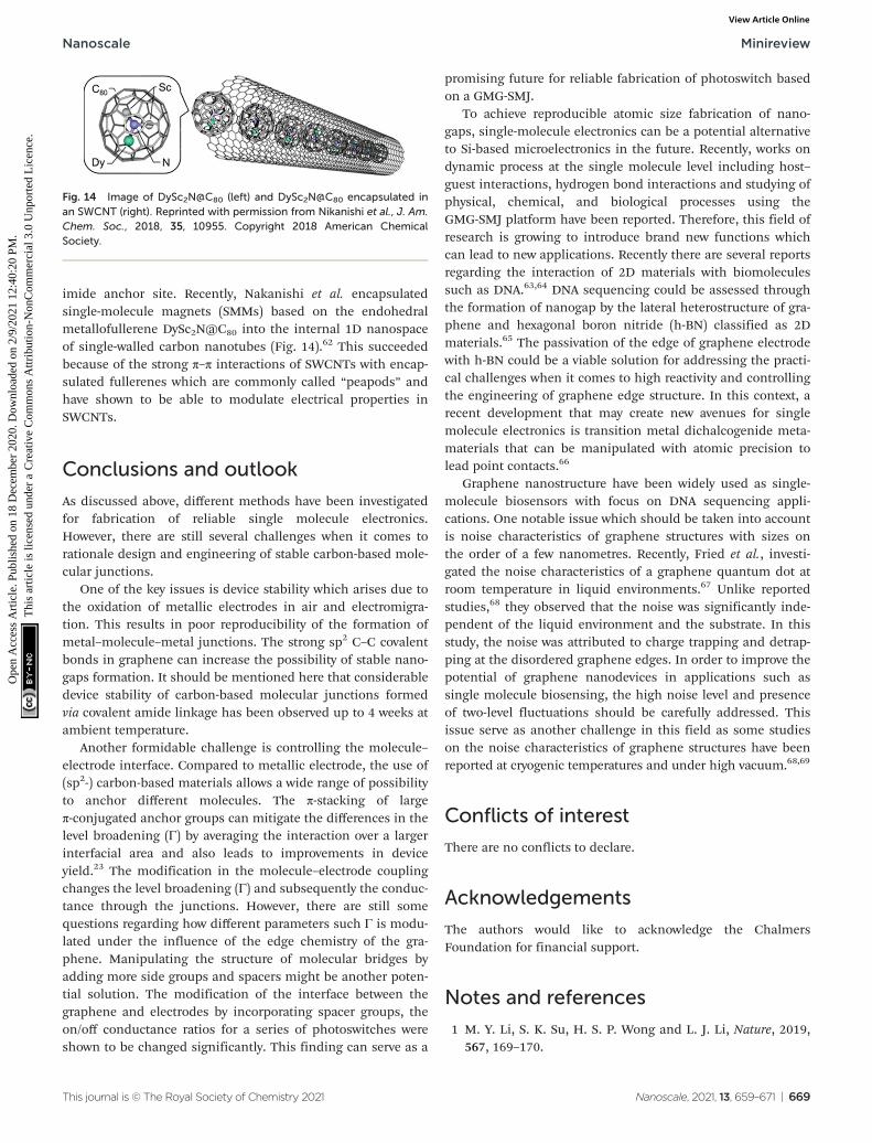
Freeley et al. conducted a study to investigate the covalentcoupling of single proteins to the terminal ends of individualSWCNTs using an in-solution methodology.59 They designedtwo green fluorescent protein (sfGFP) variants to introduce anazide CNT-anchoring handle. The two GFP mutants (shortaxis, GFPSA and long axis, GFPLA) were constructed to formssDNA/SWCNT-GFP hybrids with specific protein orientations.Florescence investigation revealed the evidence of site-specificcoupling between the SWCNTs and the proteins for only theSWCNT-GFPSA nanohybrids. Recently, Thomas et al. reportedthe covalent coupling of four different fluorescent proteinsto CNT side walls through phenyl azide photochemistry(Fig. 13).60 Depending on the position of the protein on theCNT side wall, GFP function switched from GFPLA and GFPSA,which resulted in a change of the fluorescence wavelength.
Choi et al. developed an approach to monitor single-mole-cule lysozyme dynamics by attaching the molecule of interestto a field-effect transistor (FET) device using a noncovalentimmobilization based on pyrene linkers.61 The binding ofpyrenes to SWNTs through π–π stacking might pave thepathway for dilute anchor points for further derivatization ofthe surface. In this study, a thiol from a single cysteine variantof T4 lysozyme (S90C) was covalently coupled to a pyrene male-
Fig. 12 Schematic of a PPD (p-phenylenediamine)-linked molecularjunction and reactions of formation for linear junctions with one and twobringing molecules. Reprinted with permission from Zhu et al., J. Am.Chem. Soc., 2016, 9, 2905. Copyright 2016 American Chemical Society.
Fig. 13 Direct protein attachment to CNTs via phenyl azide photochemistry. Scheme of photochemical insertion of a protein via geneticallyencoded phenyl azide chemistry. Reprinted with permission from Thomas et al., Bioconjugate Chem., 2019, 3, 584.
Minireview Nanoscale
668 | Nanoscale, 2021, 13, 659–671 This journal is © The Royal Society of Chemistry 2021
Ope
n A
cces
s A
rtic
le. P
ublis
hed
on 1
8 D
ecem
ber
2020
. Dow
nloa
ded
on 2
/9/2
021
12:4
0:20
PM
. T
his
artic
le is
lice
nsed
und
er a
Cre
ativ
e C
omm
ons
Attr
ibut
ion-
Non
Com
mer
cial
3.0
Unp
orte
d L
icen
ce.
View Article Online
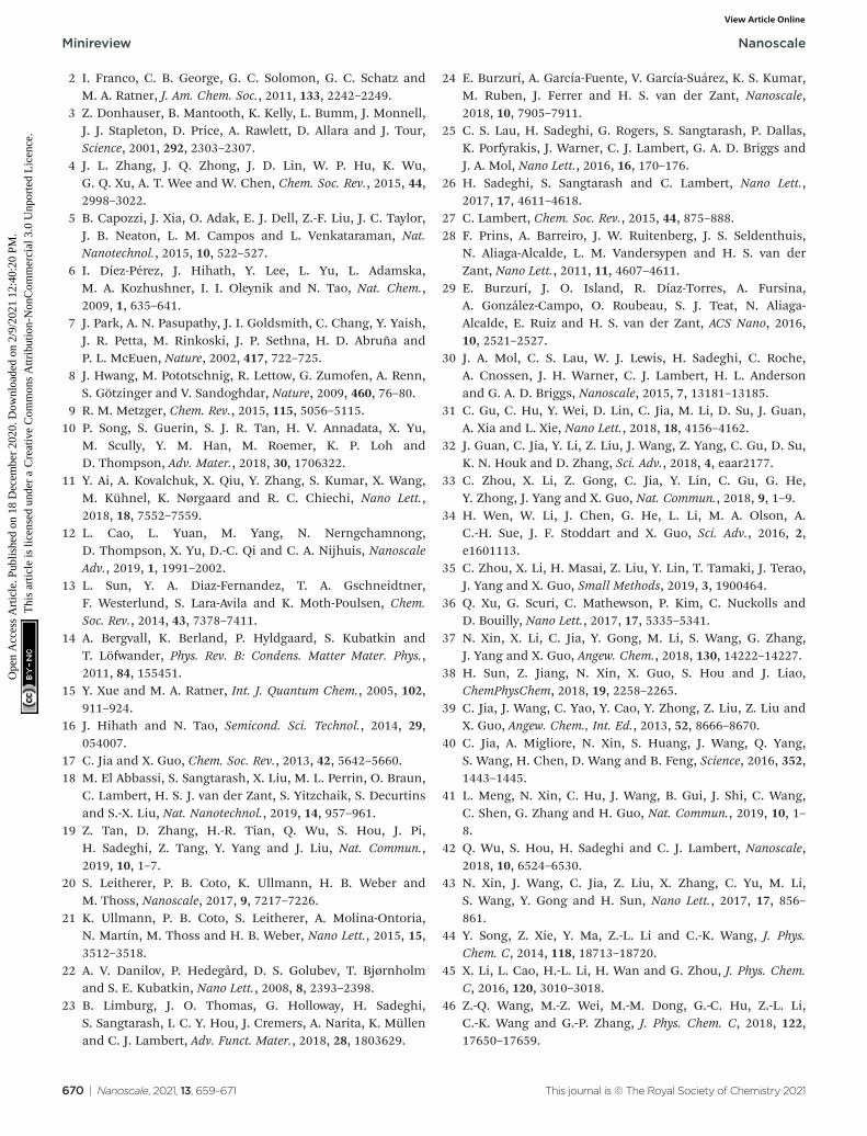
imide anchor site. Recently, Nakanishi et al. encapsulatedsingle-molecule magnets (SMMs) based on the endohedralmetallofullerene DySc2N@C80 into the internal 1D nanospaceof single-walled carbon nanotubes (Fig. 14).62 This succeededbecause of the strong π–π interactions of SWCNTs with encap-sulated fullerenes which are commonly called “peapods” andhave shown to be able to modulate electrical properties inSWCNTs.
Conclusions and outlook
As discussed above, different methods have been investigatedfor fabrication of reliable single molecule electronics.However, there are still several challenges when it comes torationale design and engineering of stable carbon-based mole-cular junctions.
One of the key issues is device stability which arises due tothe oxidation of metallic electrodes in air and electromigra-tion. This results in poor reproducibility of the formation ofmetal–molecule–metal junctions. The strong sp2 C–C covalentbonds in graphene can increase the possibility of stable nano-gaps formation. It should be mentioned here that considerabledevice stability of carbon-based molecular junctions formedvia covalent amide linkage has been observed up to 4 weeks atambient temperature.
Another formidable challenge is controlling the molecule–electrode interface. Compared to metallic electrode, the use of(sp2-) carbon-based materials allows a wide range of possibilityto anchor different molecules. The π-stacking of largeπ-conjugated anchor groups can mitigate the differences in thelevel broadening (Γ) by averaging the interaction over a largerinterfacial area and also leads to improvements in deviceyield.23 The modification in the molecule–electrode couplingchanges the level broadening (Γ) and subsequently the conduc-tance through the junctions. However, there are still somequestions regarding how different parameters such Γ is modu-lated under the influence of the edge chemistry of the gra-phene. Manipulating the structure of molecular bridges byadding more side groups and spacers might be another poten-tial solution. The modification of the interface between thegraphene and electrodes by incorporating spacer groups, theon/off conductance ratios for a series of photoswitches wereshown to be changed significantly. This finding can serve as a
promising future for reliable fabrication of photoswitch basedon a GMG-SMJ.
To achieve reproducible atomic size fabrication of nano-gaps, single-molecule electronics can be a potential alternativeto Si-based microelectronics in the future. Recently, works ondynamic process at the single molecule level including host–guest interactions, hydrogen bond interactions and studying ofphysical, chemical, and biological processes using theGMG-SMJ platform have been reported. Therefore, this field ofresearch is growing to introduce brand new functions whichcan lead to new applications. Recently there are several reportsregarding the interaction of 2D materials with biomoleculessuch as DNA.63,64 DNA sequencing could be assessed throughthe formation of nanogap by the lateral heterostructure of gra-phene and hexagonal boron nitride (h-BN) classified as 2Dmaterials.65 The passivation of the edge of graphene electrodewith h-BN could be a viable solution for addressing the practi-cal challenges when it comes to high reactivity and controllingthe engineering of graphene edge structure. In this context, arecent development that may create new avenues for singlemolecule electronics is transition metal dichalcogenide meta-materials that can be manipulated with atomic precision tolead point contacts.66
Graphene nanostructure have been widely used as single-molecule biosensors with focus on DNA sequencing appli-cations. One notable issue which should be taken into accountis noise characteristics of graphene structures with sizes onthe order of a few nanometres. Recently, Fried et al., investi-gated the noise characteristics of a graphene quantum dot atroom temperature in liquid environments.67 Unlike reportedstudies,68 they observed that the noise was significantly inde-pendent of the liquid environment and the substrate. In thisstudy, the noise was attributed to charge trapping and detrap-ping at the disordered graphene edges. In order to improve thepotential of graphene nanodevices in applications such assingle molecule biosensing, the high noise level and presenceof two-level fluctuations should be carefully addressed. Thisissue serve as another challenge in this field as some studieson the noise characteristics of graphene structures have beenreported at cryogenic temperatures and under high vacuum.68,69
Conflicts of interest
There are no conflicts to declare.
Acknowledgements
The authors would like to acknowledge the ChalmersFoundation for financial support.
Notes and references
1 M. Y. Li, S. K. Su, H. S. P. Wong and L. J. Li, Nature, 2019,567, 169–170.
Fig. 14 Image of DySc2N@C80 (left) and DySc2N@C80 encapsulated inan SWCNT (right). Reprinted with permission from Nikanishi et al., J. Am.Chem. Soc., 2018, 35, 10955. Copyright 2018 American ChemicalSociety.
Nanoscale Minireview
This journal is © The Royal Society of Chemistry 2021 Nanoscale, 2021, 13, 659–671 | 669
Ope
n A
cces
s A
rtic
le. P
ublis
hed
on 1
8 D
ecem
ber
2020
. Dow
nloa
ded
on 2
/9/2
021
12:4
0:20
PM
. T
his
artic
le is
lice
nsed
und
er a
Cre
ativ
e C
omm
ons
Attr
ibut
ion-
Non
Com
mer
cial
3.0
Unp
orte
d L
icen
ce.
View Article Online
2 I. Franco, C. B. George, G. C. Solomon, G. C. Schatz andM. A. Ratner, J. Am. Chem. Soc., 2011, 133, 2242–2249.
3 Z. Donhauser, B. Mantooth, K. Kelly, L. Bumm, J. Monnell,J. J. Stapleton, D. Price, A. Rawlett, D. Allara and J. Tour,Science, 2001, 292, 2303–2307.
4 J. L. Zhang, J. Q. Zhong, J. D. Lin, W. P. Hu, K. Wu,G. Q. Xu, A. T. Wee and W. Chen, Chem. Soc. Rev., 2015, 44,2998–3022.
5 B. Capozzi, J. Xia, O. Adak, E. J. Dell, Z.-F. Liu, J. C. Taylor,J. B. Neaton, L. M. Campos and L. Venkataraman, Nat.Nanotechnol., 2015, 10, 522–527.
6 I. Díez-Pérez, J. Hihath, Y. Lee, L. Yu, L. Adamska,M. A. Kozhushner, I. I. Oleynik and N. Tao, Nat. Chem.,2009, 1, 635–641.
7 J. Park, A. N. Pasupathy, J. I. Goldsmith, C. Chang, Y. Yaish,J. R. Petta, M. Rinkoski, J. P. Sethna, H. D. Abruña andP. L. McEuen, Nature, 2002, 417, 722–725.
8 J. Hwang, M. Pototschnig, R. Lettow, G. Zumofen, A. Renn,S. Götzinger and V. Sandoghdar, Nature, 2009, 460, 76–80.
9 R. M. Metzger, Chem. Rev., 2015, 115, 5056–5115.10 P. Song, S. Guerin, S. J. R. Tan, H. V. Annadata, X. Yu,
M. Scully, Y. M. Han, M. Roemer, K. P. Loh andD. Thompson, Adv. Mater., 2018, 30, 1706322.
11 Y. Ai, A. Kovalchuk, X. Qiu, Y. Zhang, S. Kumar, X. Wang,M. Kühnel, K. Nørgaard and R. C. Chiechi, Nano Lett.,2018, 18, 7552–7559.
12 L. Cao, L. Yuan, M. Yang, N. Nerngchamnong,D. Thompson, X. Yu, D.-C. Qi and C. A. Nijhuis, NanoscaleAdv., 2019, 1, 1991–2002.
13 L. Sun, Y. A. Diaz-Fernandez, T. A. Gschneidtner,F. Westerlund, S. Lara-Avila and K. Moth-Poulsen, Chem.Soc. Rev., 2014, 43, 7378–7411.
14 A. Bergvall, K. Berland, P. Hyldgaard, S. Kubatkin andT. Löfwander, Phys. Rev. B: Condens. Matter Mater. Phys.,2011, 84, 155451.
15 Y. Xue and M. A. Ratner, Int. J. Quantum Chem., 2005, 102,911–924.
16 J. Hihath and N. Tao, Semicond. Sci. Technol., 2014, 29,054007.
17 C. Jia and X. Guo, Chem. Soc. Rev., 2013, 42, 5642–5660.18 M. El Abbassi, S. Sangtarash, X. Liu, M. L. Perrin, O. Braun,
C. Lambert, H. S. J. van der Zant, S. Yitzchaik, S. Decurtinsand S.-X. Liu, Nat. Nanotechnol., 2019, 14, 957–961.
19 Z. Tan, D. Zhang, H.-R. Tian, Q. Wu, S. Hou, J. Pi,H. Sadeghi, Z. Tang, Y. Yang and J. Liu, Nat. Commun.,2019, 10, 1–7.
20 S. Leitherer, P. B. Coto, K. Ullmann, H. B. Weber andM. Thoss, Nanoscale, 2017, 9, 7217–7226.
21 K. Ullmann, P. B. Coto, S. Leitherer, A. Molina-Ontoria,N. Martín, M. Thoss and H. B. Weber, Nano Lett., 2015, 15,3512–3518.
22 A. V. Danilov, P. Hedegård, D. S. Golubev, T. Bjørnholmand S. E. Kubatkin, Nano Lett., 2008, 8, 2393–2398.
23 B. Limburg, J. O. Thomas, G. Holloway, H. Sadeghi,S. Sangtarash, I. C. Y. Hou, J. Cremers, A. Narita, K. Müllenand C. J. Lambert, Adv. Funct. Mater., 2018, 28, 1803629.
24 E. Burzurí, A. García-Fuente, V. García-Suárez, K. S. Kumar,M. Ruben, J. Ferrer and H. S. van der Zant, Nanoscale,2018, 10, 7905–7911.
25 C. S. Lau, H. Sadeghi, G. Rogers, S. Sangtarash, P. Dallas,K. Porfyrakis, J. Warner, C. J. Lambert, G. A. D. Briggs andJ. A. Mol, Nano Lett., 2016, 16, 170–176.
26 H. Sadeghi, S. Sangtarash and C. Lambert, Nano Lett.,2017, 17, 4611–4618.
27 C. Lambert, Chem. Soc. Rev., 2015, 44, 875–888.28 F. Prins, A. Barreiro, J. W. Ruitenberg, J. S. Seldenthuis,
N. Aliaga-Alcalde, L. M. Vandersypen and H. S. van derZant, Nano Lett., 2011, 11, 4607–4611.
29 E. Burzurí, J. O. Island, R. Díaz-Torres, A. Fursina,A. González-Campo, O. Roubeau, S. J. Teat, N. Aliaga-Alcalde, E. Ruiz and H. S. van der Zant, ACS Nano, 2016,10, 2521–2527.
30 J. A. Mol, C. S. Lau, W. J. Lewis, H. Sadeghi, C. Roche,A. Cnossen, J. H. Warner, C. J. Lambert, H. L. Andersonand G. A. D. Briggs, Nanoscale, 2015, 7, 13181–13185.
31 C. Gu, C. Hu, Y. Wei, D. Lin, C. Jia, M. Li, D. Su, J. Guan,A. Xia and L. Xie, Nano Lett., 2018, 18, 4156–4162.
32 J. Guan, C. Jia, Y. Li, Z. Liu, J. Wang, Z. Yang, C. Gu, D. Su,K. N. Houk and D. Zhang, Sci. Adv., 2018, 4, eaar2177.
33 C. Zhou, X. Li, Z. Gong, C. Jia, Y. Lin, C. Gu, G. He,Y. Zhong, J. Yang and X. Guo, Nat. Commun., 2018, 9, 1–9.
34 H. Wen, W. Li, J. Chen, G. He, L. Li, M. A. Olson, A.C.-H. Sue, J. F. Stoddart and X. Guo, Sci. Adv., 2016, 2,e1601113.
35 C. Zhou, X. Li, H. Masai, Z. Liu, Y. Lin, T. Tamaki, J. Terao,J. Yang and X. Guo, Small Methods, 2019, 3, 1900464.
36 Q. Xu, G. Scuri, C. Mathewson, P. Kim, C. Nuckolls andD. Bouilly, Nano Lett., 2017, 17, 5335–5341.
37 N. Xin, X. Li, C. Jia, Y. Gong, M. Li, S. Wang, G. Zhang,J. Yang and X. Guo, Angew. Chem., 2018, 130, 14222–14227.
38 H. Sun, Z. Jiang, N. Xin, X. Guo, S. Hou and J. Liao,ChemPhysChem, 2018, 19, 2258–2265.
39 C. Jia, J. Wang, C. Yao, Y. Cao, Y. Zhong, Z. Liu, Z. Liu andX. Guo, Angew. Chem., Int. Ed., 2013, 52, 8666–8670.
40 C. Jia, A. Migliore, N. Xin, S. Huang, J. Wang, Q. Yang,S. Wang, H. Chen, D. Wang and B. Feng, Science, 2016, 352,1443–1445.
41 L. Meng, N. Xin, C. Hu, J. Wang, B. Gui, J. Shi, C. Wang,C. Shen, G. Zhang and H. Guo, Nat. Commun., 2019, 10, 1–8.
42 Q. Wu, S. Hou, H. Sadeghi and C. J. Lambert, Nanoscale,2018, 10, 6524–6530.
43 N. Xin, J. Wang, C. Jia, Z. Liu, X. Zhang, C. Yu, M. Li,S. Wang, Y. Gong and H. Sun, Nano Lett., 2017, 17, 856–861.
44 Y. Song, Z. Xie, Y. Ma, Z.-L. Li and C.-K. Wang, J. Phys.Chem. C, 2014, 118, 18713–18720.
45 X. Li, L. Cao, H.-L. Li, H. Wan and G. Zhou, J. Phys. Chem.C, 2016, 120, 3010–3018.
46 Z.-Q. Wang, M.-Z. Wei, M.-M. Dong, G.-C. Hu, Z.-L. Li,C.-K. Wang and G.-P. Zhang, J. Phys. Chem. C, 2018, 122,17650–17659.
Minireview Nanoscale
670 | Nanoscale, 2021, 13, 659–671 This journal is © The Royal Society of Chemistry 2021
Ope
n A
cces
s A
rtic
le. P
ublis
hed
on 1
8 D
ecem
ber
2020
. Dow
nloa
ded
on 2
/9/2
021
12:4
0:20
PM
. T
his
artic
le is
lice
nsed
und
er a
Cre
ativ
e C
omm
ons
Attr
ibut
ion-
Non
Com
mer
cial
3.0
Unp
orte
d L
icen
ce.
View Article Online

47 D. Weckbecker, P. Coto and M. Thoss, Nano Lett., 2017, 17,3341–3346.
48 L. Han, X. Zuo, H. Li, Y. Li, C. Fang and D. Liu, J. Phys.Chem. C, 2019, 123, 2736–2745.
49 J. Li, N. Friedrich, N. Merino, D. G. de Oteyza, D. Peña,D. Jacob and J. I. Pascual, Nano Lett., 2019, 19, 3288–3294.
50 X. Guo, J. P. Small, J. E. Klare, Y. Wang, M. S. Purewal,I. W. Tam, B. H. Hong, R. Caldwell, L. Huang andS. O’Brien, Science, 2006, 311, 356–359.
51 A. K. Feldman, M. L. Steigerwald, X. Guo and C. Nuckolls,Acc. Chem. Res., 2008, 41, 1731–1741.
52 J. Zhu, J. McMorrow, R. Crespo-Otero, G. Ao, M. Zheng,W. P. Gillin and M. Palma, J. Am. Chem. Soc., 2016, 138,2905–2908.
53 L. Zoppi, A. Ferretti and K. K. Baldridge, J. Chem. TheoryComput., 2015, 11, 4900–4910.
54 L. Medrano Sandonas, Á. Rodríguez Méndez, R. Gutierrez,J. M. Ugalde, V. Mujica and G. Cuniberti, J. Phys. Chem. C,2019, 123, 9680–9687.
55 S. Sorgenfrei, C.-Y. Chiu, M. Johnston, C. Nuckolls andK. L. Shepard, Nano Lett., 2011, 11, 3739–3743.
56 S. Vernick, S. M. Trocchia, S. B. Warren, E. F. Young,D. Bouilly, R. L. Gonzalez, C. Nuckolls and K. L. Shepard,Nat. Commun., 2017, 8, 1–9.
57 X. Guo, A. A. Gorodetsky, J. Hone, J. K. Barton andC. Nuckolls, Nat. Nanotechnol., 2008, 3, 163–167.
58 S. Sorgenfrei, C.-Y. Chiu, R. L. Gonzalez Jr., Y.-J. Yu, P. Kim,C. Nuckolls and K. L. Shepard, Nat. Nanotechnol., 2011, 6,126.
59 M. Freeley, H. L. Worthy, R. Ahmed, B. Bowen, D. Watkins,J. E. Macdonald, M. Zheng, D. D. Jones and M. Palma,J. Am. Chem. Soc., 2017, 139, 17834–17840.
60 S. K. Thomas, W. D. Jamieson, R. E. Gwyther, B. J. Bowen,A. Beachey, H. L. Worthy, J. E. Macdonald, M. Elliott,O. K. Castell and D. D. Jones, Bioconjugate Chem., 2019, 31,584–594.
61 Y. Choi, I. S. Moody, P. C. Sims, S. R. Hunt, B. L. Corso,I. Perez, G. A. Weiss and P. G. Collins, Science, 2012, 335,319–324.
62 R. Nakanishi, J. Satoh, K. Katoh, H. Zhang, B. K. Breedlove,M. Nishijima, Y. Nakanishi, H. Omachi, H. Shinohara andM. Yamashita, J. Am. Chem. Soc., 2018, 140, 10955–10959.
63 Q. Li, H. Liu, Y. Tian, J. Guo, G. Chen and J. Y. Lee, J. Phys.Chem. C, 2020, 124, 10823–10831.
64 R. L. Kumawat and B. Pathak, J. Phys. Chem. C, 2019, 123,22377–22383.
65 V. Shukla, N. K. Jena, A. Grigoriev and R. Ahuja, ACS Appl.Mater. Interfaces, 2017, 9, 39945–39952.
66 B. Munkhbat, A. B. Yankovich, D. G. Baranov, R. Verre,E. Olsson and T. O. Shegai, Nat. Commun., 2020, 11, 1–8.
67 J. P. Fried, X. Bian, J. L. Swett, I. I. Kravchenko,G. A. D. Briggs and J. A. Mol, Nanoscale, 2020, 12, 871–876.
68 X.-X. Song, H.-O. Li, J. You, T.-Y. Han, G. Cao, T. Tu,M. Xiao, G.-C. Guo, H.-W. Jiang and G.-P. Guo, Sci. Rep.,2015, 5, 8142.
69 P. Puczkarski, Q. Wu, H. Sadeghi, S. Hou, A. Karimi,Y. Sheng, J. H. Warner, C. J. Lambert, G. A. D. Briggs andJ. A. Mol, ACS Nano, 2018, 12, 9451–9460.
Nanoscale Minireview
This journal is © The Royal Society of Chemistry 2021 Nanoscale, 2021, 13, 659–671 | 671
Ope
n A
cces
s A
rtic
le. P
ublis
hed
on 1
8 D
ecem
ber
2020
. Dow
nloa
ded
on 2
/9/2
021
12:4
0:20
PM
. T
his
artic
le is
lice
nsed
und
er a
Cre
ativ
e C
omm
ons
Attr
ibut
ion-
Non
Com
mer
cial
3.0
Unp
orte
d L
icen
ce.
View Article Online