Embed Size (px)
Citation preview
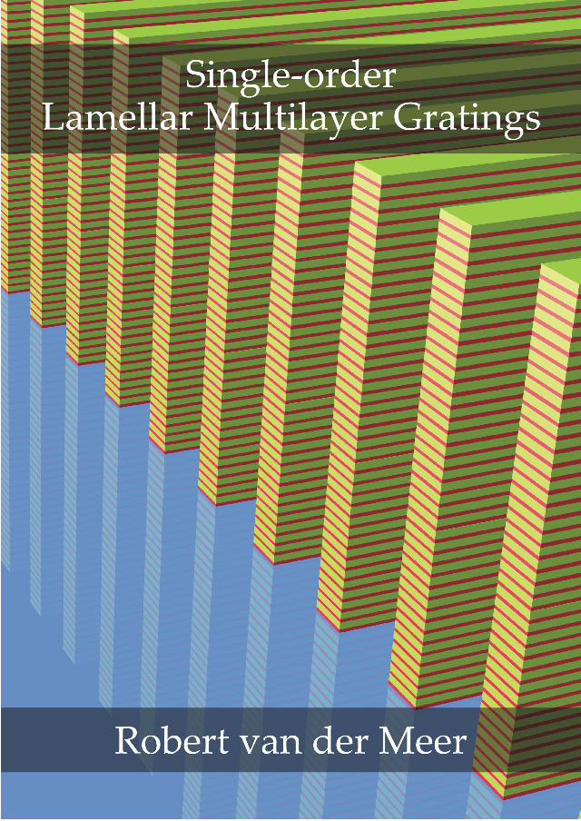

Single-orderLamellar Multilayer Gratings
door
Robert van der Meer
Ph.D. committee
Chairman & secretary:
Prof. dr. G. van der Steenhoven University of Twente
Promotor:
Prof. dr. F. BijkerkUniversity of Twente &FOM Institute DIFFER
Co-promotor:
Prof. dr. K.-J. Boller University of Twente
Members:
Prof. dr. A. I. Erko Helmholtz Zentrum Berlin
Prof. dr. H. P. Urbach Delft University of Technology
Dr. ir. E. M. C. M. Reuvekamp PANalytical
Prof. dr. ir. W. G. van der Wiel University of Twente
Prof. dr. ing. A. J. H. M. Rijnders University of Twente
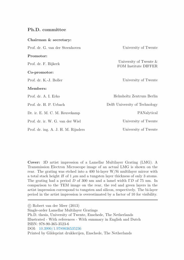
Cover: 3D artist impression of a Lamellar Multilayer Grating (LMG). ATransmission Electron Microscope image of an actual LMG is shown on therear. The grating was etched into a 400 bi-layer W/Si multilayer mirror witha total stack height H of 1 μm and a tungsten layer thickness of only 3 atoms.The grating had a period D of 300 nm and a lamel width ΓD of 75 nm. Incomparison to the TEM image on the rear, the red and green layers in theartist impression correspond to tungsten and silicon, respectively. The bi-layerperiod in the artist impression is overestimated by a factor of 10 for visibility.
c© Robert van der Meer (2013)Single-order Lamellar Multilayer GratingsPh.D. thesis, University of Twente, Enschede, The NetherlandsIllustrated - With references - With summary in English and DutchISBN: 978-90-365-3523-6DOI: 10.3990/1.9789036535236Printed by Gildeprint drukkerijen, Enschede, The Netherlands
Single-orderLamellar Multilayer Gratings
Proefschrift
ter verkrijging van
de graad van doctor aan de Universiteit Twente,
op gezag van de rector magnificus,
prof. dr. H. Brinksma,
volgens besluit van het College voor Promoties
in het openbaar te verdedigen
op vrijdag 22 maart 2013 om 12.45 uur
door
Robert van der Meer
geboren op 5 september 1985
te Aberdeen, Schotland
Dit proefschrift is goedgekeurd door de promotor
Prof. dr. F. Bijkerk
en de co-promotor
Prof. dr. K.-J. Boller
The research presented in this thesis was carried out at the Laser Physicsand Nonlinear Optics group, Department of Science and Technology, MESA+
Institute of Nanotechnology, University of Twente, P.O. Box 217, 7500 AE En-schede, The Netherlands. This research is supported by the Dutch TechnologyFoundation STW, which is part of the Netherlands Organisation for Scien-tific Research (NWO) and partly funded by the Ministry of Economic Affairs(project number #10302).
Summary
A major challenge in the soft x-ray (SXR) and eXtreme UltraViolet (XUV)spectral ranges is the ability to manipulate the incident radiation using op-tical elements. By patterning conventional multilayer mirrors with nanoscalestructures, novel optical elements with a variety of optical properties can beobtained. In this work, the design, fabrication and characterization of LamellarMultilayer Gratings (LMG) was investigated. Such LMGs are a particular formof the general class of Bragg-Fresnel optics which combine Fresnel optics withBragg reflection to provide unique dispersive and focusing optics. In particu-lar, LMGs can be used to improve the spectral resolution of x-ray fluorescencetechniques.
A Coupled Waves Approach (CWA) was derived to simulate the optical per-formance, in terms of resolution and reflectivity, of LMGs. This CWA allowedto study the physical principles behind LMGs and resulted in the identifica-tion of an optimal LMG operating regime. In this regime, the incident beamis reflected in a single diffraction order and is hence referred to as the single-order regime. Such single-order LMGs were fabricated using UV-NanoImprintLithography and Bosch Deep Reactive Ion Etching, a process chosen to en-able rapid practical development. Single-order operation was experimentallydemonstrated and showed an improvement in spectral resolution of a factor of3.8 with regard to conventional multilayer mirrors. Singe-order excitation ofhigher diffraction orders was also measured and analyzed.
Single-order operation often requires multilayer stacks and grating struc-tures that cannot be fabricated with sufficient accuracy using current tech-nologies. As this invalidates the semi-infinite multilayer approximation, weinvestigated the optical performance of LMGs with finite multilayer stacks.We determined the ratio between the absorber thickness and bi-layer period ofthe multilayer stack can be used to further tailor LMG optical performance tomaximize bandwidth reduction or minimize peak reflectivity loss. We also in-vestigated various degradation processes that could limit the lifetime of LMGs,which is important for the applicability of such elements. Oxidation of tung-sten and silicon as well as changes to the sidewall composition were clearly seen.However, SXR reflectivity remained stable to within measurement accuracy foran extended storage period of 18 months in a 1 atm air environment. The pos-sibility of applying a capping layer on LMG structures to reduce degradationwas also studied.

Samenvatting
Een grote uitdaging in het zachte rontgen (SXR) en eXtreme UltraViolet(XUV) golflengte gebied is de mogelijkheid om deze straling te manipulerendoor middel van optische elementen. Door conventionele multilaag spiegels testructureren kunnen nieuwe optische elementen gemaakt worden met een groteverscheidenheid in het optisch gedrag. In dit werk is het ontwerp, fabricageen karakterisatie van de zogenoemde Lamellaire Multilaag Tralies (LMG) on-derzocht. Zulke LMGs zijn een specifieke vorm van Bragg-Fresnel elementendie Fresnel optica combineert met Bragg reflectie om zo unieke dispersieve enfocuserende eigenschappen te verkrijgen. In het bijzonder kunnen deze LMGsworden gebruikt om de spectrale resolutie van rontgen fluoresentie techniekente verbeteren.
Een theorie genaamd Gekoppelde Golven Aanpak (CWA) is afgeleid om hetoptisch gedrag, in termen van resolutie en reflectiviteit, van LMGs te kunnensimuleren. Deze CWA maakt het mogelijk om de optica van LMG elementente bestuderen. Optimaal LMG gedrag wordt bereikt in het enkelvoudige-orderegime, waarin de inkomende rontgenbundel slechts een diffractie orde exci-teert. Deze enkelvoudige-orde LMGs zijn vervolgens gefabriceerd met UV-NanoImprint Lithografie en Bosch Deep Reactive Ion Etching. Hiermee is dewerking in het enkelvoudige orde voor het eerst experimenteel aangetoond. Ditleidde tot een verbetering in spectrale resolutie met een factor 3.8 in vergelijk-ing met conventionele multilaagspiegels. Het gebruik van hogere orders is ookbestudeerd en geanalyseerd.
Het enkelvoudige-orde regime vergt multilagen en tralie structuren die nietmet de huidige technieken voldoende accuraat gemaakt kunnen worden. Desemi-oneindige multilaag benadering is daardoor niet altijd geldig en wij hebbendaarom het optisch gedrag van LMGs met een eindige multilaag bestudeerd.Uit deze analyse hebben wij bepaald dat de verhouding tussen de dikte van deabsorberende component en de bi-laag periode van de multilaag gebruikt kanworden om LMG optisch gedrag verder te optimaliseren voor kleine tralie struc-turen. Tot slot hebben wij degradatieprocessen onderzocht die de levensduurvan LMGs zouden kunnen verminderen. Hoewel er duidelijke veranderingenin de compositie van de zijlaag en oxidatie is waargenomen, bleef de SXR re-flectie stabiel binnen de meetnauwkeurigheid gedurende een opslagperiode van18 maanden in een 1 atm lucht omgeving. Het gebruik van een beschermendeafdeklaag op LMGs tegen degradatie is ook onderzocht.

Publications
I Journal papers
• I. V. Kozhevnikov, R. van der Meer, H. M. J. Bastiaens, K.-J. Bollerand F. Bijkerk, “High-resolution, high-reflectivity operation of lamellarmultilayer amplitude gratings: identification of the single-order regime”,Optics Express, vol. 18, no. 15, pp. 16234-16242, 2010
• II. V.V. Kozhevnikov, R. van der Meer, H. M. J. Bastiaens, K.-J.Boller and F. Bijkerk, “Analytic theory of soft x-ray diffraction by lamel-lar multilayer gratings”, Optics Express, vol. 19, no. 10, pp. 9172-9184,2011
• R. van der Meer, I. V. Kozhevnikov, B. Krishnan, J. Huskens, P. E.Hegeman, G. C. S. Brons, B. Vratzov, H. M. J. Bastiaens, K.-J. Boller andF. Bijkerk, “Single-order operation of lamellar multilayer gratings in thesoft x-ray spectral range”, AIP Advances, vol. 3, no. 1, pp. 012103-1/7,2013
• R. van der Meer, I. V. Kozhevnikov et al., “Reflection of soft x-raysfrom non-ideal Lamellar Multilayer Gratings”, In preparation.
• R. van der Meer, B. Krishnan, M. J. de Boer et al., “Improved etchanisotropy in Bosch DRIE using thin-layered mixed materials”, In prepa-ration.
• R. van der Meer, I. V. Kozhevnikov et al., “Optical performance ofsingle-order lamellar multilayer gratings with finite multilayer stacks”, Inpreparation.
• R. van der Meer, I. V. Kozhevnikov et al., “Lifetime and degradationeffects in patterned W/Si multilayer mirrors”, In preparation.
• V. V. Medvedev, A. J. R. van den Boogaard, R. van der Meer, A. E.Yakshin, E. Louis, V. M. Krivtsun, A. M. Yakunin and F. Bijkerk, “In-frared phase-shift filtering for Extreme UltraViolet multilayer Bragg re-flectors”, In preparation.
vi Publications
II Patents
• F. Bijkerk, W. G. van der Wiel, R. van der Meer and P. E. Hegeman,“Method for manufacturing a multilayer structure with a lateral patternfor application in the XUV wavelength range, and BF and LMAG struc-tures manufactured according to this method”, International patent WO2011/071380, Priority date: 11/12/2009, Publication date: 16/06/2011
• F. van Goor, F. Bijkerk, A. J. R. van den Boogaard and R. van derMeer, “Spectral filter for splitting a beam with electromagnetic radiationhaving wavelengths in the extreme ultraviolet (EUV) or soft x-ray (softx) and the infrared (IR) wavelength range”, International patent WO2012/023853, Priority date: 18/08/2010, Publication date: 23/02/2012
III Conference proceedings
• R. van der Meer, B. Krishnan, I. V. Kozhevnikov, M. J. De Boer, B.Vratzov, H. M. J. Bastiaens, J. Huskens, W. G. van der Wiel, P. E. Hege-man, G. C. S. Brons, K.-J. Boller and F. Bijkerk, “Improved resolutionfor soft-x-ray monochromatization using lamellar multilayer gratings”, inAdvances in X-Ray/EUV Optics and Components VI, vol. 8139 of Proc.of SPIE, pp. 81390Q-1/8, 2011
IV Oral presentations
• R. van der Meer, I. V. Kozhevnikov, B. Vratzov, H. M. J. Bastiaens,K.-J. Boller and F. Bijkerk, “Lamellar Multilayer Amplitude Gratingsfor use in XUV optics”, EOS topical meeting on Diffractive Optics 2010,14/02/2010, Koli, Finland
• R. van der Meer, B. Krishnan, I. V. Kozhevnikov, M. J. de Boer, B.Vratzov, H. M. J. Bastiaens, J. Huskens, W. G. van der Wiel, P. E. Hege-man, G. C. S. Brons, K.-J. Boller and F. Bijkerk, “Improved resolutionfor soft-x-ray monochromatization using lamellar multilayer gratings”,FOM Veldhoven 2011, 17/01/2011, Veldhoven, the Netherlands
• R. van der Meer, B. Krishnan, I. V. Kozhevnikov, M. J. de Boer, B.Vratzov, H. M. J. Bastiaens, J. Huskens, W. G. van der Wiel, P. E. Hege-man, G. C. S. Brons, K.-J. Boller and F. Bijkerk, “Improved resolutionfor soft-x-ray spectroscopy: single-order operation of lamellar multilayergratings”, EOS topical meeting on Diffractive Optics 2012, 27/02/2012,Delft, the Netherlands
• R. van der Meer, B. Krishnan, I. V. Kozhevnikov, M. J. de Boer, B.Vratzov, H. M. J. Bastiaens, J. Huskens, W. G. van der Wiel, P. E.
V Poster presentations vii
Hegeman, G. C. S. Brons, K.-J. Boller and F. Bijkerk, “Etching of W/Simultilayer mirrors for the fabrication of lamellar multilayer gratings”,Micro and NanoEngineering 2012, 17/09/2012, Toulouse, France
• R. van der Meer, B. Krishnan, I. V. Kozhevnikov, M. J. de Boer, B.Vratzov, H. M. J. Bastiaens, J. Huskens, G. P. M. Roelofs, P. V. San-tos, W. G. van der Wiel, P. E. Hegeman, G. C. S. Brons, K.-J. Bollerand F. Bijkerk, “Advantages of UV-NanoImprint Lithography and dual-source dry etching for novel applications”, MicroNanoConference 2012,10/12/2012, Ede, the Netherlands
V Poster presentations
• R. van der Meer, B. Krishnan, I. V. Kozhevnikov, B. Vratzov, H. M. J.Bastiaens, J.Huskens, W. G. van der Wiel, K.-J. Boller and F. Bijkerk,“Fabrication of lamellar multilayer gratings using UV-NIL and modi-fied Bosch etching”, MicroNanoConference, 17-18/10/2010, Enschede,the Netherlands
• P. F. Moonen, B. Krishnan, B. Vratzov, R. van der Meer, K.-J. Boller,W. G. van der Wiel, H. M. J. Bastiaens, W. T. T. Smaal, M. Peter, D.Turkenburg, E. R. Meinders, F. Bijkerk and J. Huskens, “Nanofabrica-tion by Step-and-flash Imprint Lithography”, MESA+ annual meeting,14/09/2010, Enschede, the Netherlands
• R. van der Meer, B. Krishnan, I. V. Kozhevnikov, B. Vratzov, H. M. J.Bastiaens, J. Huskens, W. G. van der Wiel, K.-J. Boller and F. Bijkerk,“Improved resolution for soft-x-ray monochromatization using lamellarmultilayer gratings”, NNV Plasma physics, 15-16/03/2011, Lunteren, theNetherlands
• R. van der Meer, B. Krishnan, I. V. Kozhevnikov, M. J. de Boer, B.Vratzov, H. M. J. Bastiaens, J. Huskens, W. G. van der Wiel, P. E. Hege-man, G. C. S. Brons, K.-J. Boller and F. Bijkerk, “Improved resolutionfor soft-x-ray monochromatization using lamellar multilayer gratings”,SPIE Optics and Photonics, 21-25/08/2011, San Diego, United States
• R. van der Meer, B. Krishnan, I. V. Kozhevnikov, M. J. de Boer, B.Vratzov, H. M. J. Bastiaens, J. Huskens, W. G. van der Wiel, P. E. Hege-man, G. C. S. Brons, K.-J. Boller and F. Bijkerk, “Improved resolutionfor soft-x-ray monochromatization using lamellar multilayer gratings”,MESA+ annual meeting, 27/09/2011, Enschede, the Netherlands
• R. van der Meer, B. Krishnan, I. V. Kozhevnikov, M. J. de Boer, B.Vratzov, H. M. J. Bastiaens, J.Huskens, W. G. van der Wiel, P. E. Hege-man, G. C. S. Brons, K.-J. Boller and F. Bijkerk, “Improved resolution
viii Publications
for soft-x-ray monochromatization using lamellar multilayer gratings”,MicroNanoConference, 15-16/11/2011, Ede, the Netherlands
• R. van der Meer, B. Krishnan, I. V. Kozhevnikov, M. J. de Boer, B.Vratzov, H. M. J. Bastiaens, J.Huskens, W. G. van der Wiel, P. E. Hege-man, G. C. S. Brons, K.-J. Boller and F. Bijkerk, “Reduced bandwidthsfor soft-x ray reflection using Lamellar Multilayer Gratings”, NNV plasmaphysics, 06-07/03/2012, Lunteren, the Netherlands
• H. M. J. Bastiaens, R. van der Meer, B. Vratzov and F. Bijkerk, “Highline density free-standing transmission gratings for EUV emission spec-troscopy”, International Symposium on Extreme Ultraviolet Lithography,30/09-04/10/2012, Brussels, Belgium
Contents
Summary i
Samenvatting iii
Publications v
I Journal papers . . . . . . . . . . . . . . . . . . . . . . . . . . . v
II Patents . . . . . . . . . . . . . . . . . . . . . . . . . . . . . . . vi
III Conference proceedings . . . . . . . . . . . . . . . . . . . . . . vi
IV Oral presentations . . . . . . . . . . . . . . . . . . . . . . . . . vi
V Poster presentations . . . . . . . . . . . . . . . . . . . . . . . . vii
1 Introduction 1
1.1 Motivation . . . . . . . . . . . . . . . . . . . . . . . . . . . . . 1
1.2 X-ray optics . . . . . . . . . . . . . . . . . . . . . . . . . . . . . 2
1.2.1 Multilayer mirrors . . . . . . . . . . . . . . . . . . . . . 2
1.2.2 Diffractive optics . . . . . . . . . . . . . . . . . . . . . . 4
1.2.3 Lamellar Multilayer Gratings . . . . . . . . . . . . . . . 7
1.3 Applications . . . . . . . . . . . . . . . . . . . . . . . . . . . . . 8
1.3.1 X-ray fluorescence spectroscopy . . . . . . . . . . . . . . 8
1.3.2 X-ray imaging . . . . . . . . . . . . . . . . . . . . . . . 9
1.3.3 EUV lithography . . . . . . . . . . . . . . . . . . . . . . 10
1.4 Thesis outline . . . . . . . . . . . . . . . . . . . . . . . . . . . . 10
2 Experimental 13
2.1 Introduction . . . . . . . . . . . . . . . . . . . . . . . . . . . . . 13
2.2 Optical performance and multilayer structure characterization . 13
2.2.1 Soft x-ray reflectometry . . . . . . . . . . . . . . . . . . 13
2.2.2 Grazing incidence x-ray reflectometry . . . . . . . . . . 14
2.3 LMG structure characterization . . . . . . . . . . . . . . . . . . 15
2.3.1 Stylus profilometry . . . . . . . . . . . . . . . . . . . . . 15
2.3.2 Scanning electron microscopy . . . . . . . . . . . . . . . 15
x CONTENTS
2.3.3 Transmission electron microscopy . . . . . . . . . . . . . 16
2.3.4 X-ray photoelectron spectroscopy . . . . . . . . . . . . . 17
3 Theory of Lamellar Multilayer Gratings 19
3.1 Introduction . . . . . . . . . . . . . . . . . . . . . . . . . . . . . 19
3.2 Coupled waves approach . . . . . . . . . . . . . . . . . . . . . . 20
3.2.1 Basic equations . . . . . . . . . . . . . . . . . . . . . . . 20
3.2.2 Generalized equations . . . . . . . . . . . . . . . . . . . 23
3.2.3 Numerical solution . . . . . . . . . . . . . . . . . . . . . 25
3.2.4 Analytical solution . . . . . . . . . . . . . . . . . . . . . 26
3.2.5 Analytic description of LMG optical performance . . . . 30
3.2.6 Interfacial roughness . . . . . . . . . . . . . . . . . . . . 31
3.2.7 CWA validity for p-polarized radiation . . . . . . . . . . 32
3.3 Single-order LMG operation . . . . . . . . . . . . . . . . . . . . 34
3.4 Conclusions . . . . . . . . . . . . . . . . . . . . . . . . . . . . . 36
4 Fabrication of gratings in W/Si multilayer mirrors 37
4.1 Introduction . . . . . . . . . . . . . . . . . . . . . . . . . . . . . 37
4.2 Experimental . . . . . . . . . . . . . . . . . . . . . . . . . . . . 38
4.3 Etching and scalloping in Bosch DRIE . . . . . . . . . . . . . . 39
4.4 Determination of fabrication criteria . . . . . . . . . . . . . . . 40
4.4.1 Generalized Coupled Waves Approach . . . . . . . . . . 41
4.4.2 Optical effect of tapering . . . . . . . . . . . . . . . . . 42
4.4.3 Optical effect of scalloping . . . . . . . . . . . . . . . . . 44
4.4.4 Fabrication criteria for W/Si LMGs . . . . . . . . . . . 46
4.5 Etching of W/Si ML mirrors . . . . . . . . . . . . . . . . . . . 47
4.5.1 Etch settings . . . . . . . . . . . . . . . . . . . . . . . . 47
4.5.2 Comparison of ML with silicon etching . . . . . . . . . . 48
4.5.3 Control of scallop formation . . . . . . . . . . . . . . . . 51
4.5.4 Minimizing profile taper . . . . . . . . . . . . . . . . . . 52
4.5.5 Reduction of grating structure dependence . . . . . . . 53
4.6 Conclusions . . . . . . . . . . . . . . . . . . . . . . . . . . . . . 53
5 Experimental demonstration of single-order LMG operation 55
5.1 Introduction . . . . . . . . . . . . . . . . . . . . . . . . . . . . . 55
5.2 Single versus multi-order operation . . . . . . . . . . . . . . . . 55
5.3 Single-order Γ scaling . . . . . . . . . . . . . . . . . . . . . . . 57
5.4 Bi-layer period accuracy . . . . . . . . . . . . . . . . . . . . . . 58
5.5 Energy dependence of LMG performance . . . . . . . . . . . . 59
CONTENTS xi
5.6 Higher diffraction orders . . . . . . . . . . . . . . . . . . . . . . 60
5.7 Conclusions . . . . . . . . . . . . . . . . . . . . . . . . . . . . . 62
6 Performance of finite stack Lamellar Multilayer Gratings 63
6.1 Introduction . . . . . . . . . . . . . . . . . . . . . . . . . . . . . 63
6.2 Semi-infinite approximation . . . . . . . . . . . . . . . . . . . . 64
6.2.1 Reflection from single-order LMGs . . . . . . . . . . . . 64
6.2.2 Analytical description of optical performance . . . . . . 65
6.2.3 Simulation of semi-infinite LMGs . . . . . . . . . . . . . 67
6.3 Finite ML stacks . . . . . . . . . . . . . . . . . . . . . . . . . . 67
6.3.1 Simulation of LMGs with finite ML stacks . . . . . . . . 67
6.3.2 Tailoring of performance with the γ-ratio . . . . . . . . 69
6.4 Conclusions . . . . . . . . . . . . . . . . . . . . . . . . . . . . . 70
7 Lifetime of patterned W/Si multilayer mirrors 73
7.1 Introduction . . . . . . . . . . . . . . . . . . . . . . . . . . . . . 73
7.2 Potential degradation processes . . . . . . . . . . . . . . . . . . 74
7.2.1 Sidewall contamination . . . . . . . . . . . . . . . . . . 74
7.2.2 Thermal annealing . . . . . . . . . . . . . . . . . . . . . 80
7.2.3 Oxygen diffusion . . . . . . . . . . . . . . . . . . . . . . 83
7.2.4 Stability of SXR reflectivity over time . . . . . . . . . . 84
7.3 Capping layers . . . . . . . . . . . . . . . . . . . . . . . . . . . 85
7.3.1 Possible capping materials . . . . . . . . . . . . . . . . . 85
7.3.2 Preliminary silicon nitride deposition tests . . . . . . . . 86
7.4 Conclusions . . . . . . . . . . . . . . . . . . . . . . . . . . . . . 88
8 Conclusions 89
References 93
Dankwoord/Acknowledgments 103

1Introduction
1.1 Motivation
The ability to identify and quantify chemical elements in products is very im-portant to ensure, for instance, that steel and concrete are of sufficient qualityto be used for construction and that there are no toxic contaminants in our foodor drinks. One of the earliest methods used to identify elements is the flametest in which a sample is positioned in a hot, transparent flame. The heat fromthe flame breaks chemical bonds to create free atoms and also excites theseatoms into excited electronic states. When these atoms return to the groundstate, they emit light at characteristic wavelengths. For example, calcium willproduce a yellow-red colored flame whereas copper produces a green flame andlead results in a bluish-white flame. However, the range of detectable elementsis small and the sample is burned during the measurement [1].
A major improvement in chemical element identification was achieved afterthe discovery of x-rays. Henry Moseley determined in 1914 that there wasa relationship between the atomic number Z of elements and the energy offluorescent x-rays emitted after an element was irradiated by high energy x-rays [2, 3]. Elements could now be uniquely and non-destructively identified byanalyzing the fluorescent x-ray spectrum, which is the basic principle of x-rayfluorescence spectroscopy as described in more detail in section 1.3.1.
To analyze the fluorescence spectrum, an optical element is required thatseparates x-rays with different energies. Such elements are typically naturalcrystals or ML mirrors which work based on the well-known principle of Braggdiffraction as discussed in more detail in section 1.2.1. The energy of fluorescentx-rays depend on the difference in binding energies of the electron orbitals foreach specific element. Due to their electronic configuration, lighter elements
2 Introduction
can be identified best in the soft x-ray (SXR) spectral range, i.e. at energiesbetween roughly 100 and 1500 eV. Unfortunately, the spectral resolution ofML mirrors in this regime is inherently limited by absorption of the fluorescentx-rays that need to be analyzed [4–7]. Although the natural line widths offluorescent x-rays are typically E/ΔE ≈ 1000 [8], closely spaced lines couldoften not be distinguished due to the limited resolution of the analyzing opticalelement.
The spectral resolution of ML mirrors can be improved by fabricating agrating into the ML stack, resulting in a so-called Lamellar Multilayer Grating(LMG). Although this concept has long been known [9–12], the implementationof LMGs has been hampered by two main challenges. The first was limitationsof previous simulation methods, which provided limited insights in LMG op-erating principles and could only be used for idealized LMG structures. Thesecond main challenge was the lack of a reproducible LMG fabrication methodwith accurate dimension control that is suitable for grating periods well below1 μm and can be used to economically pattern large area’s (tens of mm2).
The usability of LMGs has been significantly improved by the simulationand fabrication method that will be presented in this thesis. We derived a Cou-pled Waves Analysis (CWA) method which can be used to simulate reflectionand diffraction from LMGs and circumvents the aforementioned limitations.This CWA also resulted in improved understanding of LMG working principlesand was used to identify an optimal operating regime. In this regime, the in-cident beam excites only a single diffraction order and is hence referred to asthe single-order regime. We also developed a novel fabrication process basedon UV-NanoImprint Lithography and Bosch Deep Reactive Ion Etching, whichprovided reproducible and cost-effective fabrication of single-order operatingLMGs with grating periods down to 200 nm. With our LMGs, we achievedspectral resolutions E/ΔE of up to 330 as compared to previously reportedvalues of 70 [13] for conventional ML mirrors.
Although we focused on LMGs, this study can be considered as a pilotcase study for other optical elements that can be fabricated using the processpresented in this thesis and that also combine Bragg reflection and diffraction.
1.2 X-ray optics
LMGs are a specific type of optical element in the general class of Bragg-Fresneloptics in which Bragg reflection by a ML mirror is combined with a diffractiveoptical element. In this section, we first examine the reflection from ML mirrorsand discuss the basic principles of diffraction in some more detail.
1.2.1 Multilayer mirrors
A multilayer (ML) mirror consists of a stack of at least two different materialsthat provide multiple reflecting surfaces. One of the materials is generally
1.2 X-ray optics 3
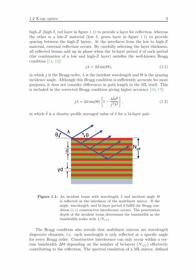
high-Z (high δ, red layer in figure 1.1) to provide a layer for reflection, whereasthe other is a low-Z material (low δ, green layer in figure 1.1) to providespacing between the high-Z layers. At the interfaces from the low to high-Zmaterial, external reflection occurs. By carefully selecting the layer thickness,all reflected beams add up in phase when the bi-layer period d of each period(the combination of a low and high-Z layer) satisfies the well-known Braggcondition [14, 15]:
jλ = 2d sin(Θ), (1.1)
in which j is the Bragg order, λ is the incident wavelength and Θ is the grazingincidence angle. Although this Bragg condition is sufficiently accurate for mostpurposes, it does not consider differences in path length in the ML itself. Thisis included in the corrected Bragg condition giving higher accuracy [16, 17]:
jλ = 2d sin(Θ)
[1− 4δd2
j2λ2
], (1.2)
in which δ is a density profile averaged value of δ for a bi-layer pair.
Figure 1.1: An incident beam with wavelength λ and incident angle Θis reflected at the interfaces of the multilayer mirror. If theangle, wavelength, and bi-layer period d fulfill the Bragg con-dition (1.1) constructive interference occurs. The penetrationdepth of the incident beam determines the bandwidth as thebandwidth scales with 1/Neff .
The Bragg condition also reveals that multilayer mirrors are wavelengthdispersive elements, i.e. each wavelength is only reflected at a specific anglefor every Bragg order. Constructive interference can only occur within a cer-tain bandwidth ΔΘ depending on the number of bi-layers (Neff ) effectivelycontributing to the reflection. The spectral resolution of a ML mirror, defined
4 Introduction
as λ/Δλ, scales with Neff [18, 19]. However, absorption in the SXR is ac-tually relatively high and maximum SXR path lengths through materials arein the order of only a few μm. This limits Neff , resulting in typical spectralresolutions around 50-100 [13].
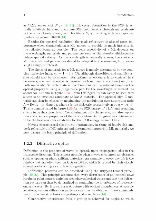
Besides the spectral resolution, the peak reflectivity is also of great im-portance when characterizing a ML mirror to provide as much intensity inthe reflected beam as possible. The peak reflectivity of a ML depends onthe wavelength, materials and parameters such as the absorber-thickness-to-bi-layer-period ratio γ. As the wavelength is generally known, the choice ofML materials and parameters should be adapted to the wavelength, or wave-length range, of interest.
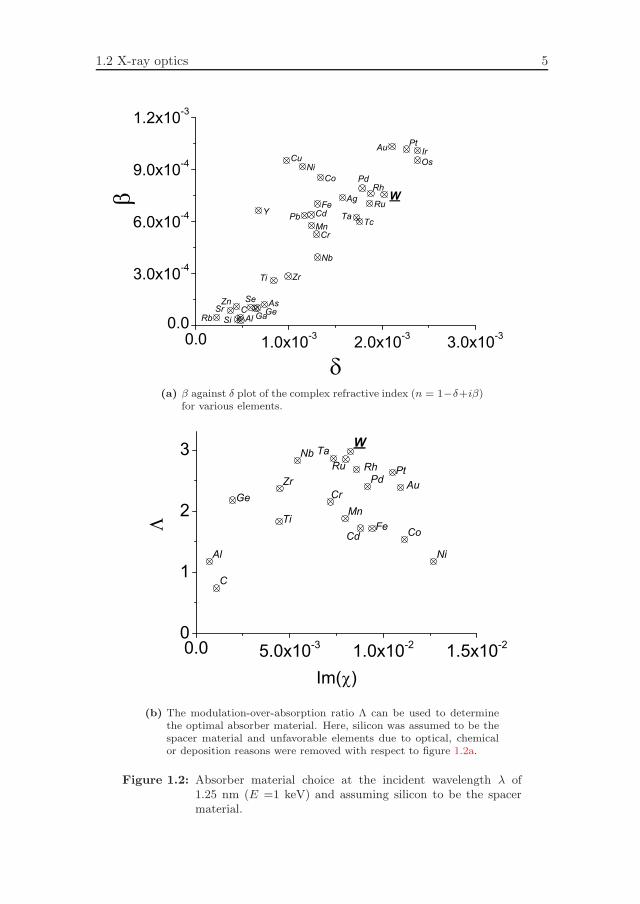
The choice of materials for a ML mirror is mainly determined by the com-plex refractive index (n = 1 − δ + iβ), although deposition and stability is-sues should also be considered. For optimal reflection, a large contrast in δbetween spacer and absorber is required with minimal absorption (low β) inboth materials. Suitable material combinations can be selected based on theoptical properties using a β against δ plot for the wavelength of interest, asshown for 1.25 nm in figure 1.2a. From this figure, it can easily be seen thatsilicon is an excellent candidate as low-Z material. The optimal high-Z ma-terial can then be chosen by maximizing the modulation-over-absorption ratioΛ = Re|εA− εS |/Im(εA), where ε is the dielectric constant given by n =
√ε [4].
This is demonstrated in figure 1.2b for the SXR energy of 1 keV and assumingsilicon to be the spacer layer. Considering not only the Λ-ratio, but also deposi-tion and chemical properties of the various elements, tungsten was determinedto be the best absorber candidate for the SXR energy around 1 keV.
Having characterized the optical performance, in terms of bandwidth andpeak reflectivity, of ML mirrors and determined appropriate ML materials, wenext discuss the basic principle of diffraction.
1.2.2 Diffractive optics
Diffraction is the property of waves to spread, upon propagation, also in thetransverse direction. This is most notable when a wave encounters an obstacle,such as opaque or phase shifting materials. An example in every day life is therainbow pattern often seen on CDs or DVDs, which is caused by their closelyspaced tracks acting as a diffraction grating.
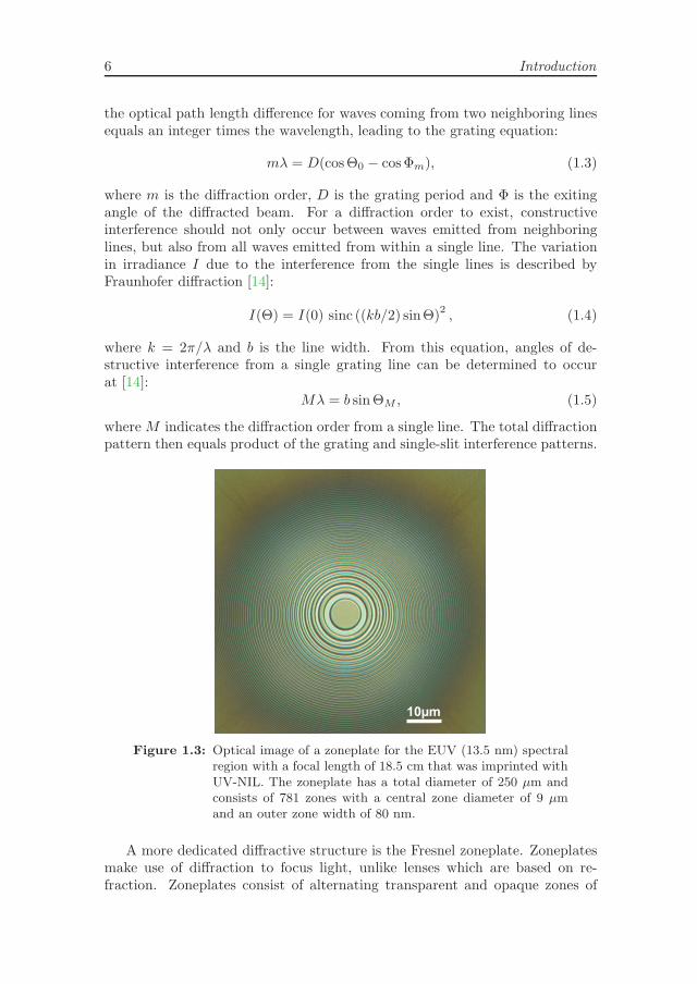
Diffraction patterns can be described using the Huygens-Fresnel princi-ple [20–22]. This principle assumes that every disturbance of an incident waveresults in point sources emitting secondary spherical waves and that the diffrac-tion pattern can then be determined by examining the interference of these sec-ondary waves. By fabricating a structure with optical disturbances at specificlocations, various diffraction patterns can thus be obtained. Two commonlyused diffractive structures are gratings and zoneplates [14].
Constructive interference from a grating is achieved for angles at which
1.2 X-ray optics 5
(a) β against δ plot of the complex refractive index (n = 1−δ+iβ)for various elements.
(b) The modulation-over-absorption ratio Λ can be used to determinethe optimal absorber material. Here, silicon was assumed to be thespacer material and unfavorable elements due to optical, chemicalor deposition reasons were removed with respect to figure 1.2a.
Figure 1.2: Absorber material choice at the incident wavelength λ of1.25 nm (E =1 keV) and assuming silicon to be the spacermaterial.
6 Introduction
the optical path length difference for waves coming from two neighboring linesequals an integer times the wavelength, leading to the grating equation:
mλ = D(cosΘ0 − cosΦm), (1.3)
where m is the diffraction order, D is the grating period and Φ is the exitingangle of the diffracted beam. For a diffraction order to exist, constructiveinterference should not only occur between waves emitted from neighboringlines, but also from all waves emitted from within a single line. The variationin irradiance I due to the interference from the single lines is described byFraunhofer diffraction [14]:
I(Θ) = I(0) sinc ((kb/2) sinΘ)2 , (1.4)
where k = 2π/λ and b is the line width. From this equation, angles of de-structive interference from a single grating line can be determined to occurat [14]:
Mλ = b sinΘM , (1.5)
where M indicates the diffraction order from a single line. The total diffractionpattern then equals product of the grating and single-slit interference patterns.
Figure 1.3: Optical image of a zoneplate for the EUV (13.5 nm) spectralregion with a focal length of 18.5 cm that was imprinted withUV-NIL. The zoneplate has a total diameter of 250 μm andconsists of 781 zones with a central zone diameter of 9 μmand an outer zone width of 80 nm.
A more dedicated diffractive structure is the Fresnel zoneplate. Zoneplatesmake use of diffraction to focus light, unlike lenses which are based on re-fraction. Zoneplates consist of alternating transparent and opaque zones of
1.2 X-ray optics 7
increasing radius and decreasing width around a central opaque zone. As aresult, the exiting angle for constructive interference from each zone is slightlydifferent, which gives zoneplates a focusing effect. The resolution of a zone-plate is determined by the width Δr of the outermost zone and is given by1.22 ·Δrouter [14, 16].
1.2.3 Lamellar Multilayer Gratings
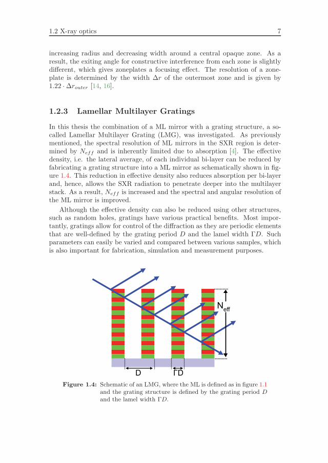
In this thesis the combination of a ML mirror with a grating structure, a so-called Lamellar Multilayer Grating (LMG), was investigated. As previouslymentioned, the spectral resolution of ML mirrors in the SXR region is deter-mined by Neff and is inherently limited due to absorption [4]. The effectivedensity, i.e. the lateral average, of each individual bi-layer can be reduced byfabricating a grating structure into a ML mirror as schematically shown in fig-ure 1.4. This reduction in effective density also reduces absorption per bi-layerand, hence, allows the SXR radiation to penetrate deeper into the multilayerstack. As a result, Neff is increased and the spectral and angular resolution ofthe ML mirror is improved.
Although the effective density can also be reduced using other structures,such as random holes, gratings have various practical benefits. Most impor-tantly, gratings allow for control of the diffraction as they are periodic elementsthat are well-defined by the grating period D and the lamel width ΓD. Suchparameters can easily be varied and compared between various samples, whichis also important for fabrication, simulation and measurement purposes.
Figure 1.4: Schematic of an LMG, where the ML is defined as in figure 1.1and the grating structure is defined by the grating period Dand the lamel width ΓD.
8 Introduction
1.3 Applications
The main application of LMGs is x-ray fluorescence spectroscopy. However,the general class of Bragg-Fresnel optics can be used in a much wider rangeof potential applications, such as x-ray imaging in microscopes, synchrotronbeamlines and astronomy. The patterning of ML mirrors can also be used inEUV lithography to separate EUV and infrared radiation. These applicationsare briefly discussed below.
1.3.1 X-ray fluorescence spectroscopy
X-ray fluorescence spectroscopy (XRF) is a technique that is used to determinethe presence and concentration of elements in a sample. This identification isachieved by measuring characteristic x-rays emitted from inner shell electrontransitions. Hard x-rays with energies up to tens of keV are used to knockout inner shell electrons from atom’s in the sample. The resulting vacancy is(primarily) filled by electrons from the next higher shell. This results in anenergy loss for the electron, which is released as a secondary, or fluorescent,x-ray photon. As the energy of this fluorescent photon is determined by thedifference in binding energies of the electron shells, the emitted photons havevery characteristic energies that depend on the specific atom and typically havenarrow natural widths of E/ΔE ≈ 1000 [8]. The energy range to be analyzed isthus determined by the atomic properties and specifically lighter elements emitmany characteristic x-rays in the SXR spectral range due to their electronicconfiguration [23].
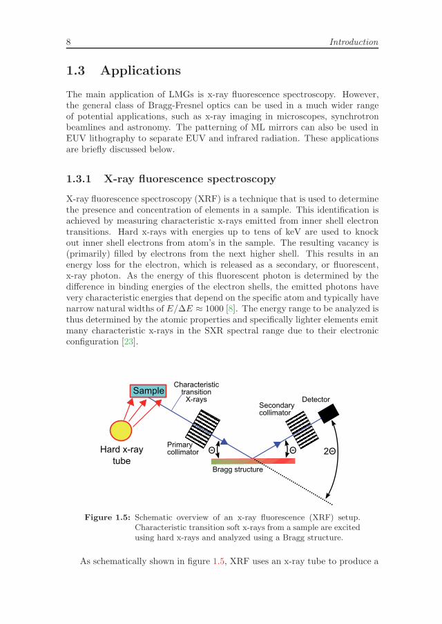
Figure 1.5: Schematic overview of an x-ray fluorescence (XRF) setup.Characteristic transition soft x-rays from a sample are excitedusing hard x-rays and analyzed using a Bragg structure.
As schematically shown in figure 1.5, XRF uses an x-ray tube to produce a
1.3 Applications 9
primary beam of high energy hard x-rays that irradiates a sample to knock outthe inner shell electrons. The resulting emitted fluorescent radiation is thenanalyzed using a wavelength dispersive Bragg structure, typically a naturalcrystal or ML mirror, and an x-ray detector. ML mirrors used in the softx-ray spectral range generally can achieve spectral resolutions in the order of50-100 [13]. However, various elements and isotopes have closely spaced shellemission lines that require spectral resolutions of at least a few hundred to beresolved [24]. As discussed in section 1.2.3, LMGs can provide such improvedspectral resolution and can therefore be highly beneficial for the identificationof elements in XRF.
1.3.2 X-ray imaging
Another possible application for the general class of Bragg-Fresnel optics are x-ray microscopes. Such microscopes are devices comparable to standard visiblelight microscopes, except for the wavelength at which they are operated. Theyuse various optical elements to focus light from a source onto a sample and thenimage that sample onto a detector. The major advantage of using x-rays canbe seen in Rayleigh’s resolution criterion, which states the minimum featuresize (Δx) that one can still distinguish is given by [25]:
Δx =0.610λ
NA(1.6)
where NA is the numerical aperture of the optical system. The factor 0.610originates from the principal properties of a perfect lens [14] and is often re-placed by an empirical constant for complex optical systems. From this equa-tion, it can be seen that by reducing the wavelength, one can significantlyimprove the resolution.
Unfortunately, Rayleigh’s criterion is not the only relevant factor in imaging.For instance, a certain amount of optical contrast between different parts of thesample is also required as well as sufficient transmission through the sample. Avery important example is the so-called water window between the oxygen andcarbon absorption edges (λ = 2.4 - 4.4 nm), in which biological samples can beimaged very well [26]. In this region, the penetration depth of SXR throughwater is about 10 μm, which is just enough to transmit through a completecell. Using x-ray microscopes, high-resolution images of complete and (at themoment of exposure) living cells can be obtained. Although other techniques,such as electron microscopy, can also produce very high resolution images, theyrequire the cell to be cut into small slices and therefore loose information withrespect to the actual working of a living cell.
Comparable optical elements to those used in soft x-ray microscopes [27–30]are also used in hard x-ray imaging at synchrotron beamlines [31–35] and invarious astronomy applications [36–38]. These applications can thus all benefitfrom the possibility to pattern ML mirrors with diffractive structures to obtainBragg-Fresnel optics.
10 Introduction
1.3.3 EUV lithography
A final important application where patterning of ML mirrors may be of in-terest is EUV lithography (EUVL). EUVL is an emerging technology to pro-duce denser computer memory and faster processor chips. To achieve this,the critical dimensions of the transistors in these chips need to be as small aspossible. These critical dimensions are again determined by the Rayleigh cri-terion (Eq. (1.6)), resulting in a continuous search for lithography techniquesat shorter wavelengths to create smaller transistors. For this, the EUV wave-length of choice is 13.5 nm, which has been selected because of its proximity tothe Si−L absorption edge. This allows for the use of ML mirrors with siliconspacers and high reflectivities. Indeed, Mo/Si ML mirrors have a theoreti-cal reflectivity of 74% and a value of 70.5% has already been experimentallydemonstrated [39]. Although this reflectivity is already very close to the theo-retical maximum, up to eleven optical elements are used in the EUV imagingsystem resulting in a very low overall transmission of < 3%.
In the last years, several EUVL systems have been shipped to various testfacilities and producers. However, these devices are mainly used to test theproduction process as these machines are not yet economically feasible due tothe limited throughput. A major challenge for improving the throughput is thelimited power available from current EUV sources. Most promising is a sourcethat uses a CO2-laser to heat and ionize tin droplets that subsequently emitEUV. Unfortunately, this means the EUV needs to be collected and separatedfrom the 10.6 μm infrared radiation (IR) coming form the CO2-laser.
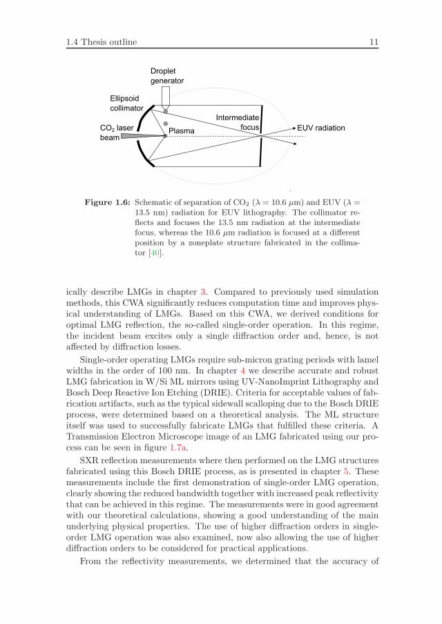
A possible solution to this challenge is to fabricate optical elements forthe 10.6 μm radiation into ML mirrors for the EUV range. For example, the10.6 μm radiation can be separated from the EUV by covering the collimatorellipsoid with a Fresnel zone reflector as shown in figure 1.6 [40]. The 10.6 μmradiation is then focused at a different position, i.e. not at the intermediatefocus, as compared to the EUV and be considerably attenuated by the exitaperture at the intermediate focus. In principle, the 10.6 μm radiation canactually be re-used by designing the setup such that the focus coincides withthe plasma. The focused CO2 radiation is then also used to heat the plasmawhich can significantly improve the efficiency of the source [40]. The principlesof IR suppression with limited EUV reflection loss was recently demonstratedusing a phase-shift grating [41].
1.4 Thesis outline
In chapter 2, we present the experimental setups used throughout this thesis.Here, we first discuss the setups used to optically characterize our LamellarMultilayer Gratings. Next, the setups used to characterize the results of LMGfabrication are presented.
We then discuss the Coupled Waves Analysis (CWA) derived to theoret-
1.4 Thesis outline 11
CO2 laserbeam
Plasma
Droplet generator
Ellipsoid collimator
EUV radiationIntermediate
focus
Figure 1.6: Schematic of separation of CO2 (λ = 10.6 μm) and EUV (λ =13.5 nm) radiation for EUV lithography. The collimator re-flects and focuses the 13.5 nm radiation at the intermediatefocus, whereas the 10.6 μm radiation is focused at a differentposition by a zoneplate structure fabricated in the collima-tor [40].
ically describe LMGs in chapter 3. Compared to previously used simulationmethods, this CWA significantly reduces computation time and improves phys-ical understanding of LMGs. Based on this CWA, we derived conditions foroptimal LMG reflection, the so-called single-order operation. In this regime,the incident beam excites only a single diffraction order and, hence, is notaffected by diffraction losses.
Single-order operating LMGs require sub-micron grating periods with lamelwidths in the order of 100 nm. In chapter 4 we describe accurate and robustLMG fabrication in W/Si ML mirrors using UV-NanoImprint Lithography andBosch Deep Reactive Ion Etching (DRIE). Criteria for acceptable values of fab-rication artifacts, such as the typical sidewall scalloping due to the Bosch DRIEprocess, were determined based on a theoretical analysis. The ML structureitself was used to successfully fabricate LMGs that fulfilled these criteria. ATransmission Electron Microscope image of an LMG fabricated using our pro-cess can be seen in figure 1.7a.
SXR reflection measurements where then performed on the LMG structuresfabricated using this Bosch DRIE process, as is presented in chapter 5. Thesemeasurements include the first demonstration of single-order LMG operation,clearly showing the reduced bandwidth together with increased peak reflectivitythat can be achieved in this regime. The measurements were in good agreementwith our theoretical calculations, showing a good understanding of the mainunderlying physical properties. The use of higher diffraction orders in single-order LMG operation was also examined, now also allowing the use of higherdiffraction orders to be considered for practical applications.
From the reflectivity measurements, we determined that the accuracy of

12 Introduction
MultilayerH=1000nm
D=300nm ΓD=75nm
Substrate
(a)
20nm
(b)
Figure 1.7: Transmission Electron Microscope image of a fabricated LMGstructure. (a) A general overview of an LMG with a gratingperiod of 300 nm and a lamel width of 75 nm fabricated ina 400 bi-layer W/Si ML mirror. (b) Zoomed image of thetop of a lamel, showing the exposed sides of the ML whereenhanced degradation by surface effects or internal ML struc-ture changes can occur.
the ML deposition was limiting the achieved bandwidth and peak reflectivityfor our LMGs. In chapter 6 we therefore investigated the optical performanceof LMGs considering various practical limitations. In particular, the opticaleffect of insufficient layers to fully reflect the incident beam was determinedbased on a comparison of LMG optical performance simulations assuming asemi-infinite and finite ML stack. From this analysis, parameters that canbe used to tailor peak reflectivity and bandwidth for LMGs with finite MLstacks were determined. An experimental demonstration of the tailoring ofLMG optical performance was achieved by measuring the reflectivity of variousLMGs fabricated in two different W/Si ML mirrors.
The lifetime of LMG structures is of importance to their usability in practi-cal applications. As can be seen in figure 1.7b, the fabrication process directlyexposes the ML structure to degradation processes and also significantly in-creases the surface area between the ML and vacuum where such processes canoccur. We therefore investigated degradation effects due to fabrication and a23 month storage in a 1 atm air environment as discussed in chapter 7. Degra-dation processes were separated in surface phenomena, such as sidewall con-tamination, and internal changes to the ML structure due to thermal annealingand oxygen diffusion. The stability of SXR reflectivity was also investigated forthe duration of the storage period. A preliminary study into the use of cappinglayers to protect patterned MLs was also performed.
Finally, conclusions on ML patterning for the fabrication of Bragg-Fresneloptics for the SXR and XUV wavelengths are discussed in chapter 8.
2Experimental
2.1 Introduction
The investigation presented in this thesis required characterization of opticalperformance, in terms of bandwidth and peak reflectivity, and of the multi-layer (ML) structure of Lamellar Multilayer Gratings (LMG). These charac-terizations were mainly performed using soft and hard x-ray reflectometry aspresented in section 2.2. The fabrication of LMGs required the patterning ofsub-micron period gratings in W/Si multilayer (ML) mirrors. Various aspectsof the fabrication process were analyzed using profile measurement, imagingand spectroscopic techniques as discussed in section 2.3.
2.2 Optical performance and multilayer struc-ture characterization
Soft and hard x-ray reflectometry was used to analyze LMG optical perfor-mance and ML structure. Although both techniques work using similar prin-ciples, different information was obtained. Soft x-ray (SXR) reflectometry wasused to characterize LMG optical performance, in terms of bandwidth and peakreflectivity, and hard x-ray (HXR) reflectometry was used to analyze the MLstructure.
2.2.1 Soft x-ray reflectometry
A soft x-ray (SXR) reflectometer is schematically shown in figure 2.1 and isin principle the same as the analysis part of the XRF setup of figure 1.5. To
14 Experimental
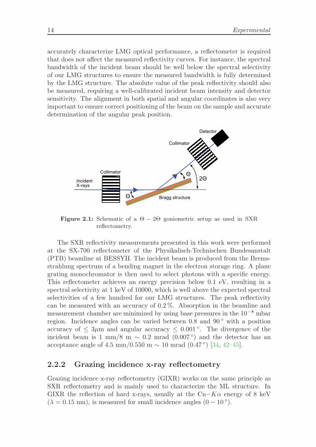
accurately characterize LMG optical performance, a reflectometer is requiredthat does not affect the measured reflectivity curves. For instance, the spectralbandwidth of the incident beam should be well below the spectral selectivityof our LMG structures to ensure the measured bandwidth is fully determinedby the LMG structure. The absolute value of the peak reflectivity should alsobe measured, requiring a well-calibrated incident beam intensity and detectorsensitivity. The alignment in both spatial and angular coordinates is also veryimportant to ensure correct positioning of the beam on the sample and accuratedetermination of the angular peak position.
Figure 2.1: Schematic of a Θ − 2Θ goniometric setup as used in SXRreflectometry.
The SXR reflectivity measurements presented in this work were performedat the SX-700 reflectometer of the Physikalisch-Technischen Bundesanstalt(PTB) beamline at BESSYII. The incident beam is produced from the Brems-strahlung spectrum of a bending magnet in the electron storage ring. A planegrating monochromator is then used to select photons with a specific energy.This reflectometer achieves an energy precision below 0.1 eV, resulting in aspectral selectivity at 1 keV of 10000, which is well above the expected spectralselectivities of a few hundred for our LMG structures. The peak reflectivitycan be measured with an accuracy of 0.2%. Absorption in the beamline andmeasurement chamber are minimized by using base pressures in the 10−8 mbarregion. Incidence angles can be varied between 0.8 and 90 ◦ with a positionaccuracy of ≤ 3μm and angular accuracy ≤ 0.001 ◦. The divergence of theincident beam is 1 mm/8 m ∼ 0.2 mrad (0.007 ◦) and the detector has anacceptance angle of 4.5 mm/0.550 m ∼ 10 mrad (0.47 ◦) [34, 42–45].
2.2.2 Grazing incidence x-ray reflectometry
Grazing incidence x-ray reflectometry (GIXR) works on the same principle asSXR reflectometry and is mainly used to characterize the ML structure. InGIXR the reflection of hard x-rays, usually at the Cu−Kα energy of 8 keV(λ = 0.15 nm), is measured for small incidence angles (0 − 10 ◦).
2.3 LMG structure characterization 15
From these measurements, the bi-layer period can be determined from thepeak positions using the corrected Bragg condition (eq. (1.2)). Below the criti-
cal angle Θc given by≈√2δ the incident beam effectively only ‘sees’ the average
material density of the top few nm, allowing for an accurate determination ofthe ML layer material composition [46, 47]. More information about the lay-ered structure, such as roughness and compound formation can be obtainedfrom simulations as derived in this work (see chapter 3) or software packageslike IMD [48].
GIXR measurements can also be performed in-situ, for instance during an-nealing tests. A reference GIXR spectrum is measured and the substrate isthen heated to the desired temperature via a hotplate in an air environment.This hotplate is capable of reaching temperatures between 25 and 900 ◦C witha 0.5 ◦C accuracy. The change in ML bi-layer period was determined by com-paring the angular positions of Bragg peaks with the reference positions. Anaccurate determination is achieved by considering relative shifts, measuring thesame Bragg orders during annealing as for the reference and using both lowand high Bragg orders [17].
2.3 LMG structure characterization
Various aspects of LMG fabrication were analyzed using height measurement,imaging and spectroscopic techniques. Height measurements were used to com-pare etching of a W/Si ML mirror and were performed using a stylus pro-filometer as presented in section 2.3.1. Electron imaging techniques, discussedin sections 2.3.2 and 2.3.3, were used to optimize the fabrication process anddetermine the spatial distribution of elements in LMGs. Finally, x-ray photo-electron spectroscopy was used to analyze the composition of the sidewfls afterLMG fabrication as discussed in section 2.3.4.
2.3.1 Stylus profilometry
When performing etch experiments, a Dektak stylus profilometer was used asa first means of determining etch results. This technique works by moving astylus with a tip radius of approximately 2.5 μm over the sample surface andmeasuring height differences as function of position. The horizontal resolu-tion is determined by various parameters of which the scan speed and heightrange are the most important. In the used setup, the resolution was 0.1% ofthe measurement range and could reach approximately 6 nm under optimalconditions [49].
2.3.2 Scanning electron microscopy
Etch results, in particular of nanostructures, were mostly characterized using aScanning Electron Microscope (SEM). In a SEM, an electron beam is typically
16 Experimental
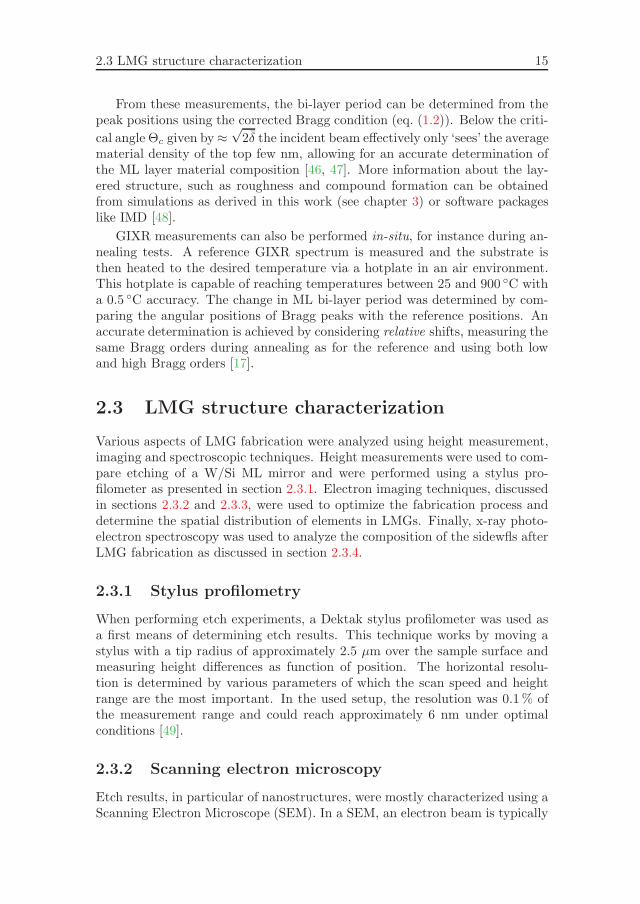
produced via thermionic emission from an electron gun fitted with a tungstenfilament cathode and has an energy ranging from 0.2 keV to several tens ofkeV. This beam is then focused using condenser lenses to a spot size of about0.4 to 5 nm. The beam is then scanned over the surface of the sample in araster pattern, where these primary electrons interact with the sample. Bothscattered and secondary electrons can be used for imaging [50]. In this thesis, aLEO 1550 high-resolution SEM was used to image fabricated LMG structures.Samples were placed under a 70 ◦ tilt, meaning the height of the structure inthe image is underestimated by 7%.
(a) (b)
Figure 2.2: SEM images of two LMG structures etched into a 1000 nmW/Si ML structure with (a) a grating period of 800 nm anda lamel width of 200 nm and (b) a grating period of 200 nmand a lamel width of 60 nm.
2.3.3 Transmission electron microscopy
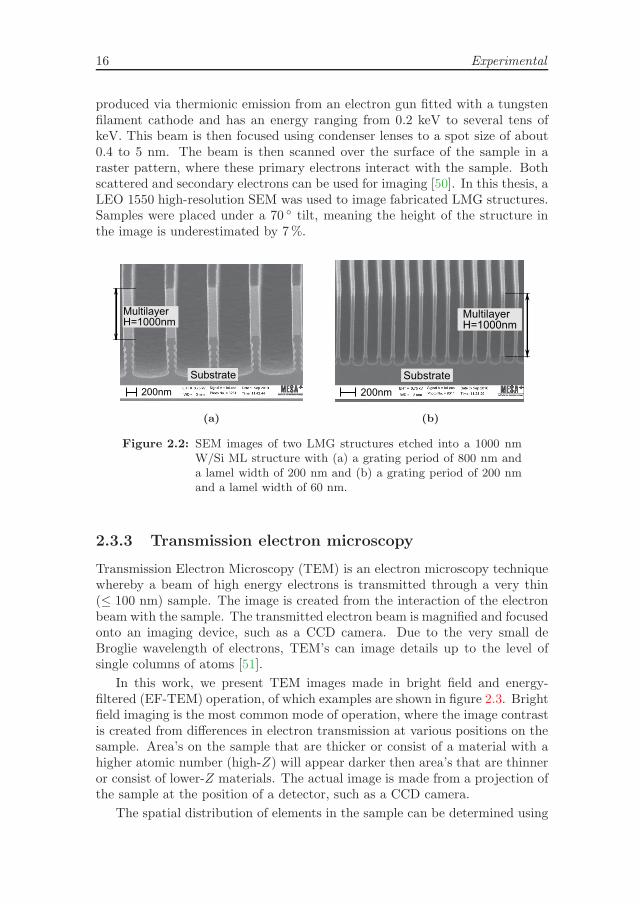
Transmission Electron Microscopy (TEM) is an electron microscopy techniquewhereby a beam of high energy electrons is transmitted through a very thin(≤ 100 nm) sample. The image is created from the interaction of the electronbeam with the sample. The transmitted electron beam is magnified and focusedonto an imaging device, such as a CCD camera. Due to the very small deBroglie wavelength of electrons, TEM’s can image details up to the level ofsingle columns of atoms [51].
In this work, we present TEM images made in bright field and energy-filtered (EF-TEM) operation, of which examples are shown in figure 2.3. Brightfield imaging is the most common mode of operation, where the image contrastis created from differences in electron transmission at various positions on thesample. Area’s on the sample that are thicker or consist of a material with ahigher atomic number (high-Z) will appear darker then area’s that are thinneror consist of lower-Z materials. The actual image is made from a projection ofthe sample at the position of a detector, such as a CCD camera.
The spatial distribution of elements in the sample can be determined using
2.3 LMG structure characterization 17
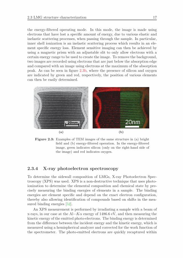
the energy-filtered operating mode. In this mode, the image is made usingelectrons that have lost a specific amount of energy, due to various elastic andinelastic scattering processes, when passing through the sample. In particular,inner shell ionization is an inelastic scattering process which results in an ele-ment specific energy loss. Element sensitive imaging can then be achieved byusing a magnetic prism with an adjustable slit to only allow electrons with acertain energy range to be used to create the image. To remove the background,two images are recorded using electrons that are just below the absorption edgeand compared with an image using electrons at the maximum of the absorptionpeak. As can be seen in figure 2.3b, where the presence of silicon and oxygenare indicated by green and red, respectively, the position of various elementscan then be easily determined.
(a) (b)
Figure 2.3: Examples of TEM images of the same structure in (a) brightfield and (b) energy-filtered operation. In the energy-filteredimage, green indicates silicon (only on the right-hand side ofthe image) and red indicates oxygen.
2.3.4 X-ray photoelectron spectroscopy
To determine the sidewall composition of LMGs, X-ray Photoelectron Spec-troscopy (XPS) was used. XPS is a non-destructive technique that uses photo-ionization to determine the elemental composition and chemical state by pre-cisely measuring the binding energies of elements in a sample. The bindingenergies are element specific and depend on the exact electron configuration,thereby also allowing identification of compounds based on shifts in the mea-sured binding energies [52].
An XPS measurement is performed by irradiating a sample with a beam ofx-rays, in our case at the Al−Kα energy of 1486.6 eV, and then measuring thekinetic energy of the emitted photo-electrons. The binding energy is determinedfrom the difference between the incident energy and the kinetic energy, which ismeasured using a hemispherical analyzer and corrected for the work function ofthe spectrometer. The photo-emitted electrons are quickly recaptured within
18 Experimental
either the sample or in air, meaning XPS requires ultra-high vacuum (UHV)conditions. Furthermore, XPS can only be used to analyze the top few nm of asample as photo-emitted electrons from deeper in the same cannot escape thesample [53].
A typical XPS spectrum thus shows the number of counted electrons plot-ted against the binding energy. The absolute energy calibration of an XPSmeasurement is very important in order to determine the exact position ofcharacteristic lines from which elements or compounds (from shifts in bind-ing energy) can be identified. The calibration is mostly done using commonlypresent elements with well-known characteristic lines, such as aliphatic carbonC1s with a characteristic line at an energy of 284.8 eV. Atomic concentrationscan be determined from the number of counted electrons and, hence, from thepeak area. However, the number of detected electrons for each element shouldfirst be divided by the empirically determined relative sensitivity factor (RSF)of that element and subsequently be normalized over all detected elements.
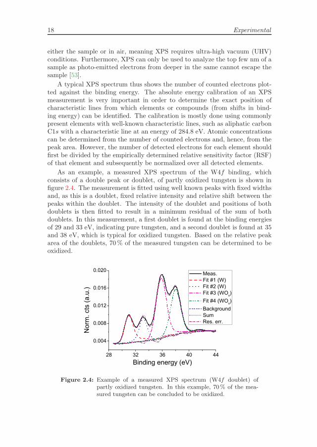
As an example, a measured XPS spectrum of the W4f binding, whichconsists of a double peak or doublet, of partly oxidized tungsten is shown infigure 2.4. The measurement is fitted using well known peaks with fixed widthsand, as this is a doublet, fixed relative intensity and relative shift between thepeaks within the doublet. The intensity of the doublet and positions of bothdoublets is then fitted to result in a minimum residual of the sum of bothdoublets. In this measurement, a first doublet is found at the binding energiesof 29 and 33 eV, indicating pure tungsten, and a second doublet is found at 35and 38 eV, which is typical for oxidized tungsten. Based on the relative peakarea of the doublets, 70% of the measured tungsten can be determined to beoxidized.
Figure 2.4: Example of a measured XPS spectrum (W4f doublet) ofpartly oxidized tungsten. In this example, 70% of the mea-sured tungsten can be concluded to be oxidized.
3Theory of
Lamellar Multilayer Gratings
3.1 Introduction
For the design of Lamellar Multilayer Gratings (LMGs) with optimal perfor-mance, in terms of bandwidth and peak reflectivity, an adequate theory for themodeling of the diffraction and reflection of the incident soft x-ray (SXR) beamis required. At present, several rigorous approaches such as modal theory orintegral method are used to simulate LMGs [54–57], in particular in the SXRregion [11, 12, 58–63]. However, the modal theory is poorly suited for LMGswith non-rectangular groove shapes or for smooth interfaces between neighbor-ing materials. Although the integral method described in ref. [57] overcomesthese problems, it is also stated that it does not suffice for the modeling ofgratings coated by hundreds of layers.
In the present chapter we describe the results of a novel LMG performanceanalysis using a Coupled Waves Approach (CWA) that does not have the afore-mentioned limitations. The equations of this method are based on a generalexpansion of the reflected field in terms of different order diffracted wavesand describe the changes in amplitude of various incident and reflected wavesthrough a system of coupled equations. This approach can be used for arbi-trary lamellar shapes, arbitrary distributions of the dielectric constant in themultilayer (ML) structure and without limitations on the grating period, lamelwidth and number of bi-layers in the ML structure. The method is well suitedfor the analysis of LMG performance in the SXR region as the diffracted peaksare narrow in this region and therefore the number of diffraction orders thatoverlap, and hence can influence each other, is limited. Note that CWA hasbeen used before successfully in SXR optics for calculations of sliced multilayer
20 Theory of Lamellar Multilayer Gratings
gratings, zone plates and holographic structures [57, 59, 64].
Using the CWA presented here, we derive that for small lamel widths LMGsoperate in a single-order regime in which there is no significant overlap of the0th diffraction order with higher orders. Only the 0th order then needs tobe considered when calculating LMG specular reflection, allowing a two-waveapproximation to be used. We show that the reflection of a SXR wave from anLMG operating in this regime simply equals the reflection from a ML mirrorwith a material density that is decreased with a factor equal to lamel-width-to-grating-period ratio Γ. Sophisticated diffraction theories are thus not necessaryfor the proper calculation of LMG performance in the single-order regime. Incontrast to what was stated in [12], we demonstrate that it is possible to derivenovel analytic design criteria for LMGs operating in the single-order regime.We also show that the resolution of an LMG operating in single-order regimeis not limited by absorption, in contrast to the resolution of a conventional MLmirror. A high resolution and high reflectivity have been shown to be mutuallyexclusive for a ML mirror [4], whereas the resolution of an LMG is only limitedby technological factors and the peak reflectivity can still be as high as for aconventional ML mirror.
In this chapter, we first derive and study the CWA in section 3.2. We beginwith the derivation of basic equations in section 3.2.1, assuming an ideal lamelprofile. More generalized equations that can be used to describe non-ideal lamelshapes and include various sidewall effects are stated next in section 3.2.2. Insections 3.2.3 and 3.2.4, both a numerical and analytical solution to the ba-sic CWA equations are presented. From the analytical solution, a generalizedBragg condition is derived in section 3.2.5 and the validity of this CWA fordifferent polarizations is investigated in section 3.2.7. Using the CWA results,a single-order operating regime has been identified, which significantly simpli-fies simulations and provides optimal LMG optical performance for practicalapplications. This operating regime is discussed in detail in section 3.3.
3.2 Coupled waves approach
3.2.1 Basic equations
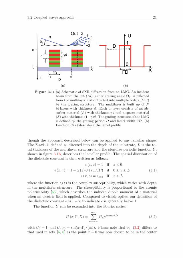
In this section, we derive the basic equations of the Coupled Waves Approach(CWA). We first define the parameters of an LMG and its geometrical repre-sentation as shown in figure 3.1a. Here, an incident beam from the left (In),under grazing angle Θ0, is reflected from the multilayer and diffracted intomultiple orders (Out) by the grating structure. The multilayer is built up fromN bi-layers with thickness d. Each bi-layer consists of an absorber material(A) with thickness γd and a spacer material (S) with thickness (1− γ)d. Thegrating structure of the LMG is defined by the grating period D and lamelwidth ΓD.
For simplicity, the basic equations assumed a rectangular lamel shape, al-
3.2 Coupled waves approach 21
(a) (b)
Figure 3.1: (a) Schematic of SXR diffraction from an LMG. An incidentbeam from the left (In), under grazing angle Θ0, is reflectedfrom the multilayer and diffracted into multiple orders (Out)by the grating structure. The multilayer is built up of Nbi-layers with thickness d. Each bi-layer consists of an ab-sorber material (A) with thickness γd and a spacer material(S) with thickness (1−γ)d. The grating structure of the LMGis defined by the grating period D and lamel width ΓD. (b)Function U(x) describing the lamel profile.
though the approach described below can be applied to any lamellar shape.The Z-axis is defined as directed into the depth of the substrate, L is the to-tal thickness of the multilayer structure and the step-like periodic function U ,shown in figure 3.1b, describes the lamellar profile. The spatial distribution ofthe dielectric constant is then written as follows:
ε (x, z) = 1 if z < 0
ε (x, z) = 1− χ (z)U (x,Γ, D) if 0 ≤ z ≤ L
ε (x, z) = εsub if z > L
(3.1)
where the function χ(z) is the complex susceptibility, which varies with depthin the multilayer structure. The susceptibility is proportional to the atomicpolarizability [65], which describes the induced dipole moment of a materialwhen an electric field is applied. Compared to visible optics, our definition ofthe dielectric constant ε is 1− χ to indicate ε is generally below 1.
The function U can be expanded into the Fourier series:
U (x,Γ, D) =
+∞∑n=−∞
Une2iπnx/D (3.2)
with U0 = Γ and Un�=0 = sin(πnΓ)/(πn). Please note that eq. (3.2) differs tothat used in refs. [5, 6] as the point x = 0 was now chosen to be in the center
22 Theory of Lamellar Multilayer Gratings
of the lamel instead of at the left side of the lamel. Shifting the coordinates ofthe previous works by x′ = x − ΓD/2 yields the same coefficients as used inthis work.
For brevity, we only considered reflection of s-polarized radiation incidentonto the LMG perpendicular to the lamels (i.e. in the plane of figure 3.1a)and the effect of interfacial roughness was neglected. The effect of p-polarizedradiation is discussed in section 3.2.7. To analyze the diffraction pattern, the2D-wave equation was solved:
∇2E (x, z) + k2ε (x, z)E (x, z) = 0, (3.3)
where the dielectric constant ε is a periodic function of x and is described byeqs. (3.1) and (3.2) and k is the wavenumber given by 2π/λ. The generalsolution then has the following form (chapter 1 in ref [66]):
F ′′n (z) + k2nFn(z) = k2χ(z)
∑m
Un−mFm(z) (3.4)
where Fn represents the field of the nth order diffraction wave. The boundaryconditions of this system signify that only plane waves from the vacuum areincident onto the LMG at the grazing angle Θ0:
F ′n(0) + iκnFn(0) = 2iκnδn,0; F ′
n(L)− iκ(s)n Fn(L) = 0. (3.5)
Here, κn =√k2 − q2n and κ
(s)n =
√k2εsub − q2n are the z-components of the
wave vectors for the nth diffraction order in vacuum and substrate, respectively,where qn = q0 + 2πn/D with q0 = k cosΘ0 and δn,0 is the Kronecker symbol.
From eq. (3.4) it can be seen that the interaction of the incident anddiffracted waves with the multilayer structure is described through the complexsusceptibility χ(z), which may be an arbitrary function, e.g. periodic or aperi-odic, step-like or smooth, etc. It can also be seen that the diffracted waves ofdifferent orders interrelate with each other and with the incident wave throughthe coefficients Un which characterize the lamellar profile. In the case of arectangular lamellar shape, the coefficients Un are numbers. For more generallamellar profiles, e.g. trapezoidal, the form of eq. (3.4) remains the same, butthe coefficients become a function of z.
As a first test of this approach, eqs. (3.4) and (3.5) were used to calculate thereflection of a conventional multilayer mirror by inserting Γ = 1. All coefficientsUn then become zero, except the coefficient U0 which then equals 1. Eq. (3.4)is then reduced to the simplest equation:
F ′′0 (z) + κ2
0F0(z) = k2χ(z)F0(z), (3.6)
which is indeed an ordinary 1D wave equation describing the reflection of awave from a conventional ML mirror, as would be expected.
Eq. (3.4) can be solved using either a numerical or, under certain approxima-tions, an analytical method. Although the numerical method is more generally
3.2 Coupled waves approach 23
valid, the analytical solution has several advantages. Most importantly, theanalytical solution allows for a preliminary physical analysis directly from thederived equations as presented in section 3.2.4.
3.2.2 Generalized equations
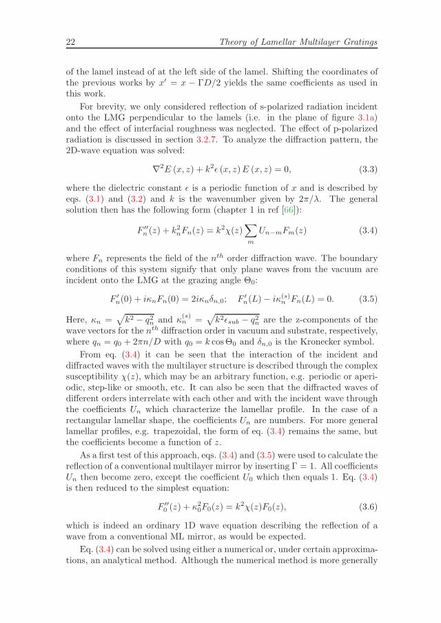
To analyze the influence of non-ideal lamel shapes on LMG reflection, we de-duced generalized CWA equations. For this, we considered a non-ideal lamelprofile as is typically the result of fabrication and which is shown schemati-cally in figure 3.2. Here, curves 1 and 2 are the sidewalls of the lamel, suchthat the space between these curves is filled by a ML structure. In addition,a layer of thickness h on the sidewalls of the lamel, indicated by curves 3 and4, was introduced. Here, we refer to these layers as being cover layers as thetheory describing these layers is valid for both contamination layers as well asdeliberately grown capping layers used to protect LMG structures. Curves 1and 3 as well as curves 2 and 4 are assumed for simplicity to be equidistant,while curves 1 and 2 (as well as 3 and 4) are mirror inverted with respect tothe Z-axis. Suppose the right side wall depicted by curve 2 is described bya single-valued function x = p(z). Then x = −p(z) can be written for theopposite wall, i.e. curve 1, and x = ∓p(z)∓ h can be written for curves 3 and4, respectively. It was assumed that the lamel width and cover layer thicknessare sufficiently small such that 2(p(z) + h) does not exceed the grating periodD at any z.
X
Z
h
H
0
ΓbottomD
ΓtopD
1 2 43
x=p(z)
Figure 3.2: Schematic cross section of a general shaped lamel. Curves1 and 2 indicate the side walls of the ML structure and aredescribed by the function p(z). A cover layer with thicknessh is indicated by curves 3 and 4. Γtop and Γbottom indicatethe Γ-ratio at the top and bottom of the lamel, respectively.
24 Theory of Lamellar Multilayer Gratings
The spatial distribution of the dielectric constant is then written as:
ε(x, z < 0) = 1; ε(x, z > H) = 1− χsub
ε(x, 0 ≤ z ≤ H) = 1− χ(z)U(x, z)− χcovV (x, z)(3.7)
where χ(z) is the susceptibility of a multilayer structure varying with the depth,while χcov and χsub are the constant susceptibility of the cover layer and sub-strate, respectively. The function U(x, z) = 1 if the point (x, z) is placedinside the multilayer structure and U = 0 otherwise. Similarly, the functionV (x, z) = 1 if the point (x, z) is placed inside the cover layer and otherwiseequals 0.
Assuming the dielectric constant to be a periodic function of x, we repre-sented the functions U and V as the Fourier series:
U(x, z) =+∞∑
n=−∞Un(z)e
2iπnx/D
V (x, z) =+∞∑
n=−∞Vn(z)e
2iπnx/D
(3.8)
where
Un(z) =1
πnsin
(2πnp(z)
D
)
Vn(z) =2
πnsin
(πnh
D
)cos
[πn
(2p(z)
D+
h
D
)] (3.9)
with U0 = 2p(z)/D and V0 = 2h/D.
Following the steps also used in section 3.2.1, the Rayleigh expansion of thefield was written as [5, 66]:
E(x, z) =+∞∑
n=−∞Fn(z)e
iqnx; qn = q0 +2πn
D
q0 = k cosΘ0; k =2π
λ
(3.10)
and eqs. (3.8)-(3.10) were substituted into the wave equation ∇2E(x, z) +k2ε(x, z) · E(x, z) = 0. An infinite system of coupled waves equations wasthen obtained:
F′′n (z) + κ2
nFn(Z) = k2∑m
[χ(z)Un−m(z) + χcovVn−m(z)]Fm(z) (3.11)
for n = 0,±1,±2, ... with the same boundary conditions as eq. (3.5). Thissystem can be used to analyze the optical effect of various imperfections arisingfrom LMG fabrication as discussed in sections 4.4 and 7.2.1.
3.2 Coupled waves approach 25
3.2.3 Numerical solution
Both systems of eqs. (3.4) and (3.11) can be solved numerically. Here, wedemonstrate the numerical solution of eq. (3.4) as this system represents anidealized LMG structure and therefore has slightly simpler equations.
We represented the field of the nth order diffraction wave Fn(z) as a super-position of two waves propagating in different directions along the z-axis.
Fn(z) = An(z)eiκnz +Bn(z)e
−iκnz (3.12)
Here, the functions An(z) and Bn(z) can vary with depth and can be consideredto be the amplitudes of a transmitted and reflected wave, respectively. Fora unique determination we imposed additional requirements to the functionsAn(z) and Bn(z) in a manner typical for the coupled waves approach:
A′n(z)e
iκnz +B′n(z)e
−iκnz = 0. (3.13)
Substituting (3.12) and (3.13) in eq. (3.4) a system of first order differentialequations for the amplitudes An and Bn was obtained:
dAn(z)
dz= − ik2
2κnχ(z)
+∞∑m=−∞
Un−m
[Am(z)ei(κm−κn)z
+Bm(z)e−i(κm−κn)z]
dBn(z)
dz= +
ik2
2κnχ(z)
+∞∑m=−∞
Un−m
[Am(z)ei(κm+κn)z
+Bm(z)e−i(κm+κn)z]
(3.14)
where n = 0,±1, ...,±∞. The boundary conditions were then written as:
An(0) = δn,0 and Bn(L) = 0 (3.15)
where we put the dielectric permeability of the substrate to unity, i.e. neglectedthe effect of the substrate on the reflection of an incident wave. This is, atleast for soft x-rays, a quite reasonable assumption as the refractive index ofmaterials is close to 1. Eqs. (3.14) is fully equivalent to the second ordersystem (3.4), but is more preferable for numerical calculations.
Evidently, the amplitudes rm and tm of the waves diffracted into vacuumand into the depth of the substrate were found by solving eqs. (3.14) withboundary conditions (3.15) to be:
rn = Bn(0), tn = An(L) (3.16)
To test the validity of the CWA derived in this section, we compared thecalculated 0th order reflectivity curves with other works [5, 12, 63]. We therefore
26 Theory of Lamellar Multilayer Gratings
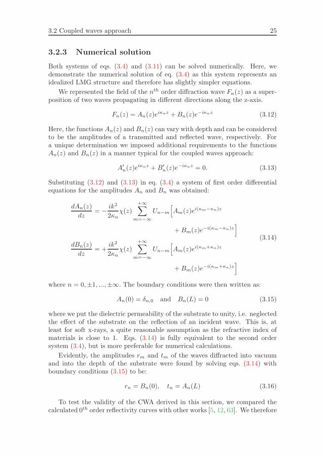
considered a Mo/B4C ML (d = 6 nm, γ = 0.33, N = 150) in which a grating isfabricated with a period D of 2 μm and a Γ of 0.3. The incident SXR energywas E = 183.4 eV and the values of the complex susceptibility χ = 1 − εused for calculations were χMo = 2.61 · 10−2 − i · 5.77 · 10−3 and χB4C =4.43 · 10−3 − i · 1.08 · 10−3. The calculations included up to the ±7 diffractionorder. As can be seen in figure 3.3, the agreement between our numericalsolution and the previous results of ref. [63] are in excellent agreement.
Figure 3.3: Calculated 0th order diffraction efficiency of a Mo/B4C LMGversus the incidence grazing angle using our numerical solu-tion (dotted line) and compared to previous results (solid line)of ref. [63].
3.2.4 Analytical solution
Eq. (3.4) can also be solved analytically for the specific case where the incidentbeam only excites a single diffraction order as discussed next. The validity ofthis assumption is discussed in section 3.3.
Zeroth order efficiency
To derive an analytical solution for the 0th order diffraction efficiency, alsoreferred to as the reflectivity, we used a two-wave approximation and onlyconsidered the incident and specularly reflected waves. The higher order termsin eqs. (3.14) were therefore neglected leading to:
dA0(z)
dz= − ik2
2κ0Γχ(z)
[A0(z) +B0(z)e
−2iκ0z]
dB0(z)
dz= +
ik2
2κ0Γχ(z)
[A0(z)e
+2iκ0z +B0(z)] (3.17)
where A0(0) = 1 and B0(L) = 0.
3.2 Coupled waves approach 27
To solve these equations, we considered a periodic multilayer structure hav-ing abrupt interfaces and consisting of two materials, namely a spacer and anabsorber, with susceptibilities χS and χA, respectively. The susceptibility ofthe ML structure is then described by
χ(z) = χS + (χA − χS)u(z), (3.18)
where the step-like function u(z) is similar to the function U that describes thelamellar profiles:
u (z, γ, d) =
+∞∑n=−∞
une2iπnz/d (3.19)
with u0 = γ and un�=0 =(1− e−2iπnγ
)/ (2iπn).
We limited ourselves to the most important case of an incident wave ontothe multilayer within or near the Bragg resonance of the jth order, i.e. wesupposed that jλ ≈ 2d sinΘ0 or, equivalently, κ0 ≈ πj/d. By substitutingeqs. (3.18) and (3.19) into eqs. (3.17), the following system was obtained:
dA0(z)
dz+
ik2
2κ0
[χΓA0(z)
+ (χA − χS)ujΓB0(z)e2i(πj/d−κ0)z
]= ΔA(z)
dB0(z)
dz− ik2
2κ0
[χΓB0(z)
+ (χA − χS)ujΓA0(z)e−2i(πj/d−κ0)z
]= ΔB(z)
(3.20)
where χ = χAγ+χS(1−γ) is the mean susceptibility of the multilayer structure.The left-hand side of eqs. (3.20) contains all terms that vary slowly with z.The functions ΔA and ΔB on the right-hand side denotes all terms oscillatingquickly with z, which, as they only weakly influence the amplitudes A0 andB0, can be neglected.
A system of coupled differential equations with constant coefficients wasthen obtained by introducing a0(z) ≡ A0(z) · e−i(πj/d−κ0)z and b0(z) ≡ B0(z) ·ei(πj/d−κ0)z:
da0(z)
dz+ i
(πj
d− κ0 +
k2
2κ0χΓ
)a0(z)
+ik2
2κ0(χA − χS) Γujb0(z) = 0
db0(z)
dz− i
(πj
d− κ0 +
k2
2κ0χΓ
)b0(z)
−ik2
2κ0(χA − χS) Γu−ja0(z) = 0
(3.21)
28 Theory of Lamellar Multilayer Gratings
with the same boundary conditions a0(0) = 1 and b0(L) = 0 as for eqs. (3.17).By solving eqs. (3.21), an analytical expression for the 0th order diffractionefficiency was obtained:
R0 =
∣∣∣∣∣ B− tanh(SNd)
b tanh(SNd)− i√B+B− − b2
∣∣∣∣∣2
(3.22)
where R0 = |r0|2. The terms used in eq. (3.22) are:
b = χΓ + 2 sinΘ0
(jλ
2d− sinΘ0
)
B± = (χA − χS) u±jΓ; S =k
2 sinΘ0
√B+B− − b2,
(3.23)
where the Bragg parameter b characterizes a deviation from the Bragg reso-nance, B± describes the modulation of the ML structure and S characterizesthe variation in amplitudes A0 and C0 with z.
Higher diffraction order efficiencies
Using a similar approach as for the analytical solution of the 0th order diffrac-tion efficiency, the higher order efficiencies could also be solved analytically. Weconsidered the mth order diffraction efficiency, where we limited ourselves toangles and wavelengths close to the Bragg resonance (quasi-Bragg resonance),i.e. assumed jλ ≈ d(sinΘ0 + sinΦm), where Φ is the diffraction angle, orequivalently κ0 + κm = 2πj/d. Here, the index j represents the Bragg reflec-tion order by the multilayer and the index m represents the diffraction orderby the grating structure.
Using a similar two-wave approximation as for the 0th order, it can beseen from eqs. (3.14) that the amplitudes A0(z) and Bm(z) only interrelateresonantly with each other and all other equations can be neglected. Then,similar to the 0th order analytic solution, we introduced a0(z) ≡ A0(z) ·e−i(πj/d−(κ0+κm)/2)z and bm(z) ≡ Bm(z) · ei(πj/d−(κ0+κm)/2)z and obtained asystem of differential equations with constant coefficients:
da0(z)
dz+ i
(πj
d− κ0 + κm
2+
k2
2κ0χΓ
)a0(z)
+ik2
2κ0(χA − χS)U−mujb0(z) = 0
db0(z)
dz− i
(πj
d− κ0 + κm
2+
k2
2κ0χΓ
)b0(z)
−ik2
2κ0(χA − χS)Umu−ja0(z) = 0
(3.24)

3.2 Coupled waves approach 29
Solving eqs. (3.24), we found an expression for the diffraction efficiency
Rm ≡ |rm|2 Re (κm/κ0), which has the same form as eq. (3.22), but has some-what different terms as those of eq. (3.23):
b =sinΘ0 + sinΦm
2√sinΘ0 sinΦm
χΓ+
2√sinΘ0 sinΦm
(jλ
2d− sinΘ0 + sinΦm
2
)
B± = (χA − χS)u±jU∓m; S =k
2√sinΘ0 sinΦm
√B+B− − b2
(3.25)
As we also did for the numerical solution, we tested the validity of the an-alytical solution by comparing this to other works. However, as the analyticalsolution is only valid within our two-wave approximation, it can only be com-pared to our numerical solution as the required grating periods (see eq. (3.39)in section 3.3) are well below the periods used in refs. [12, 63]. Figure 3.4 showsthe comparison of our numerical and analytic solutions for the same ML andΓ-ratio as used in figure 3.3, but with a reduced grating period D of 300 nm.As can be seen, the agreement between our numerical and analytical solutionis excellent. Hence, in single-order operation, sophisticated diffraction theoriesare not necessary to properly calculate LMG reflection and diffraction.
Figure 3.4: Calculated 0th and first order diffraction efficiency of aMo/B4C LMG versus the incidence grazing angle using ouranalytical solution (dotted lines) and compared to the numer-ical calculations (solid lines). The ML and Γ were the sameas for figure 3.3, but the grating period was reduced to D =300 nm to achieve single-order operation.
30 Theory of Lamellar Multilayer Gratings
3.2.5 Analytic description of LMG optical performance
Using the analytic solution of the previous section, we derived analytical equa-tions describing LMG optical performance. First, we derived a generalizedBragg condition for single-order LMGs, where we assumed a semi-infinite mul-tilayer structure (N → ∞) for simplicity. Eqs. (3.22) and (3.25) then reduceto their simplest form with tanh(SNd) = 1. As the Bragg peak is very nar-row due to the small polarizability of matter in the SXR wavelength region,we neglected the wavelength dependence of the dielectric constant inside thepeak. The reflectivity then only depends on the incidence angle and the radia-tion wavelength through the Bragg parameter b. At maximum reflectivity, wehave the condition dR0/dτ = 2Re [r∗(dr/db)(db/dτ)] (where either τ = sinΘ0
or τ = λ) and obtained a generalized Bragg condition that also includes theabsorption and refraction of radiation:
jλ
2d=
sinΘ0 + sinΦm
2− sinΘ0 + sinΦm
4 sinΘ0 sinΦmΓRe(χ)+
Re(χA − χS)
sinΘ0 + sinΦm
Im(χA − χS)
Im(χ)
sin2(πjγ)
(πj)2sin2(πmΓ)
(πm)2Γ
(3.26)
If the condition (eq. (3.26)) is fulfilled, the diffraction efficiency achievesa peak value, which can be written in a very simple manner comparable toref. [4]:
Rm,peak =1− w
1 + w;
w =
√1− y2
1 + f2y2; f =
Re(χA − χS)
Im(χA − χS);
y =Im(χA − χS)
Im(χ)
sin(πjγ)
(πj)
2√sinΘ0 sinΦm
sinΘ0 + sinΦm
sin(πmΓ)
(πm)Γ
(3.27)
Note that the peak reflectivity (eq. (3.27)) achieves its maximum possiblevalue when the parameter y is maximal and, hence, the thickness ratio γ of amultilayer structure obeys the equation:
tan(πjγ) = πj
[γ +
Im(χS)
Im(χA − χS)
](3.28)
which is well-known in the theory of conventional SXR multilayer mirrors [20,67].
From eq. (3.27), it can also be seen that the peak reflectivity (m = 0) isindependent of the grating parameters and corresponds to that of a conven-tional multilayer mirror [4]. This is because the parameters f and y entirelydetermine the peak reflectivity and are not changed if the density of both ma-terials are scaled by the same factor Γ. In contrast, the penetration depth of
3.2 Coupled waves approach 31
the radiation into the multilayer structure LMS , and therefore also the spectraland angular resolution of an LMG, is inversely proportional to Γ:
LMS = Neff · d ∼ 1
S=
λ sinΘ0
πΓIm(χ)√(1 − y2)(1 + f2y2)
(3.29)
From this equation, an approximate value for the reflection bandwidth wasalso derived. Following refs. [4, 18], the resolving power equals E/ΔE =tanΘ/Θ ≈ Neff · π/2, where Neff was defined as in eq. (3.29). Using d =λ/2 sinΘ, the following bandwidth prediction was obtained:
ΔΘLMG ≈ 2 Im(χ) Γ
sin(2Θ0)
√(1− y2)(1 + f2y2) (3.30)
From this equation, it can easily be seen that the bandwidth scales linearlywith Γ. However, the dependence on other parameters is more complicated asχ, f and y all depend on the materials and ML γ-ratio.
3.2.6 Interfacial roughness
Interfacial roughness can have a strong effect on ML reflectivity and, hence,also on that of LMGs. Using the analytical solution of section 3.2.4, the effectof interfacial roughness in the ML structure on LMG optical performance wasanalyzed. As the interfacial roughness is present in the ML structure, the effectof roughness on LMG reflectivity can be described in the same manner as fora ML mirror. In general, the peak reflectivity of a ML mirror depends on theinterfacial roughness parameters in a very complicated manner requiring exten-sive knowledge of the roughness on each individual layer to obtain a completedescription. However, there are two limiting cases when the reflectivity of arough ML mirror is expressed in a simple manner which are analyzed below.More details on the analysis of roughness on ML reflection can be found inrefs. [16, 68–70].
The first limiting case is that of totally conformal roughness at differentinterfaces with large roughness correlation lengths in the interfacial plane.“Large” means that the width of the scattering distribution is small as com-pared to the bandwidth of the Bragg peak. Then, assuming the roughnessheight to be distributed in accordance with the normal law, the reflectivity waswritten as [70]:
R(Θ) = R0(Θ)e−(4πσc sinΘ/λ)2 , (3.31)
where R0 is the reflectivity of a perfectly smooth ML mirror and σc is the rootmean square (rms) value of the conformal roughness height. The exponentialterm is referred to as the Debye-Waller factor and is only valid within specificapproximations [69, 70].
This type of roughness is considered to result in additional scattering fromthe interfacial plane. However, the large correlation length results in scattering
32 Theory of Lamellar Multilayer Gratings
within very small angles with respect to the Bragg peak angle. As the accep-tance angle of the detectors in the measurement setups (see section 2.2) used inthis work are comparatively large, this scattered radiation was still measuredby the detector. As a result, long-scale conformal roughness does not affectmeasured reflectivity curves and was therefore not considered in the fitting ofreflectivity measurements.
The second limiting case occurs when the roughness of the different inter-faces is totally non-conformal, while the correlation function of each interfaceis the same. In addition, the correlation length in the interfacial plane is sup-posed to be very small (tending to zero) and the roughness heights are againdistributed according to the normal law. To describe the effect of such rough-ness, the modulation parameter B± in eqs. 3.23 and 3.25 should be replacedby:
B±e−1/2(2πσnc/d)2 ≈ B±e−1/2(4πσnc sinΘ/λ)2 , (3.32)
where σnc is the rms value of the non-conformal roughness height and thegrazing incidence angle Θ is supposed to be large as compared with the criticalangle of the total external reflection of the ML structure. The effect of small-scale non-conformal roughness on the reflectivity is equivalent to that of asmooth transition layer placed between neighboring materials, i.e. the small-scale roughness results in increased transmittance of the incident wave intothe ML structure and, hence, in a reduction of the reflectivity. Non-conformalroughness was therefore considered in the fitting of reflectivity measurements.
3.2.7 CWA validity for p-polarized radiation
In the previous sections we have only considered reflection and diffraction ofs-polarized radiation by LMGs. Reflection and diffraction of p-polarized radi-ation was investigated by comparing the description of the dielectric constantdistribution in the LMG for both polarization states.
First, the dielectric constant distribution in the LMG for s-polarized radi-ation was derived. In accordance with eqs. (3.1) and (3.19), this distributioncan be written as a 2D Fourier series:
ε(x, z) =1− χ ·∑m
Ume2iπmx/D−
(χA − χS) ·∑m
∑j=0
Umuje2iπ(mx/D+jz/d)
(3.33)
Using the two-wave approximation of section 3.2.4, only the terms withm = 0 in the first sum and only one harmonic with fixed m and j in the secondsum are kept. The first term Γχ describes the propagation of an incident wavethrough an LMG neglecting reflection and diffraction and the second term givesthe main contribution to the diffraction efficiency under Bragg or quasi-Braggresonance jλ ≈ d(sinΘ0 + sinΦm). In order to solve the wave equation, it is
3.2 Coupled waves approach 33
then sufficient to use (instead of eq. (3.33))
ε(x, z) = 1− χ− (χA − χS)Umuje2iπ(mx/D+jz/d) (3.34)
For p-polarized radiation, the corresponding 2D wave equation is more in-volved due to the presence of first derivatives ∇2H + k2εH − ∇(ln ε) · ∇H = 0where H is the nonzero Y-component of the magnetic field perpendicular tothe plane of figure 3.1 and where ∇ ≡ ix∂/∂x + iz∂/∂z. To simplify thewave equation, we introduced a new field function H ≡ H(x, z)/
√ε(x, z),
which obeys the 2D-wave equation without the first derivatives of the field∇2H(x, z) + k2ε(x, z)H(x, z) = 0 achieved by introducing a modified functionε(x, z). It can be shown that ε(x, z) relates to the original dielectric functionas follows:
ε(x, z) ≡ ε(x, z) +1
2k2∇2ε(x, z)
ε(x, z)− 3
4k2
[ ∇ε(x, z)
]2ε2(x, z)
(3.35)
Expanding eq. (3.35) into a 2D Fourier series and keeping only linear termsof the small susceptibilities χS and χA, we obtained, instead of eq. (3.33):
ε =1− χ ·∑m
Ume2iπmx/D
[1− 1
2
(mλ
D
)2]− (χA − χS) ·
∑m
∑j=0
Umuje2iπ(mx/D+jz/d)
[1− 1
2
(jλ
d
)2
− 1
2
(mλ
D
)2] (3.36)
As before, the two-wave approximation was used to keep only specific termsfrom eq. (3.36):
ε ≈ 1−χΓ− (χA − χS)Umuje2iπ(mx/D+jz/d)·[
1− 1
2
(jλ
d
)2
− 1
2
(mλ
D
)2]≈
≈ 1− χΓ− (χA − χS)Umuje2iπ(mx/D+jz/d) cos(Θ0 +Φm)
(3.37)
Here, the resonance condition of diffraction jλ/d ≈ sinΘ0 + sinΦm and thegrating equation mλ/D = cosΦm − cosΘ0 were already taken into account.Eq. (3.37), which is valid for p-polarized light, was then compared with eq. (3.34)for s-polarized light. The comparison shows that all the expressions deducedin our CWA for s-polarized radiation are also valid for p-polarized radiation,if the dielectric modulation of the multilayer structure χA − χS is replaced by(χA−χS) cos(Θ0+Φm). This proves that, independent of the polarization, ananalytical calculation of reflection and diffraction by LMGs is possible.
Eq. (3.37) also clearly demonstrates the main feature of p-polarized radia-tion reflection, namely that at the Brewster’s angle of incidence Θ0 = π/4, the
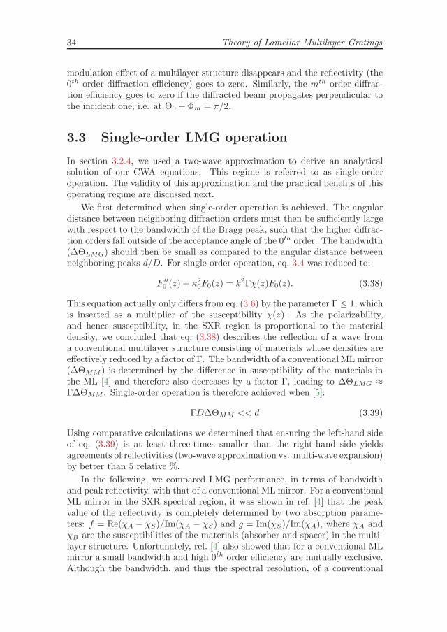
34 Theory of Lamellar Multilayer Gratings
modulation effect of a multilayer structure disappears and the reflectivity (the0th order diffraction efficiency) goes to zero. Similarly, the mth order diffrac-tion efficiency goes to zero if the diffracted beam propagates perpendicular tothe incident one, i.e. at Θ0 +Φm = π/2.
3.3 Single-order LMG operation
In section 3.2.4, we used a two-wave approximation to derive an analyticalsolution of our CWA equations. This regime is referred to as single-orderoperation. The validity of this approximation and the practical benefits of thisoperating regime are discussed next.
We first determined when single-order operation is achieved. The angulardistance between neighboring diffraction orders must then be sufficiently largewith respect to the bandwidth of the Bragg peak, such that the higher diffrac-tion orders fall outside of the acceptance angle of the 0th order. The bandwidth(ΔΘLMG) should then be small as compared to the angular distance betweenneighboring peaks d/D. For single-order operation, eq. 3.4 was reduced to:
F ′′0 (z) + κ2
0F0(z) = k2Γχ(z)F0(z). (3.38)
This equation actually only differs from eq. (3.6) by the parameter Γ ≤ 1, whichis inserted as a multiplier of the susceptibility χ(z). As the polarizability,and hence susceptibility, in the SXR region is proportional to the materialdensity, we concluded that eq. (3.38) describes the reflection of a wave froma conventional multilayer structure consisting of materials whose densities areeffectively reduced by a factor of Γ. The bandwidth of a conventional ML mirror(ΔΘMM ) is determined by the difference in susceptibility of the materials inthe ML [4] and therefore also decreases by a factor Γ, leading to ΔΘLMG ≈ΓΔΘMM . Single-order operation is therefore achieved when [5]:
ΓDΔΘMM << d (3.39)
Using comparative calculations we determined that ensuring the left-hand sideof eq. (3.39) is at least three-times smaller than the right-hand side yieldsagreements of reflectivities (two-wave approximation vs. multi-wave expansion)by better than 5 relative %.
In the following, we compared LMG performance, in terms of bandwidthand peak reflectivity, with that of a conventional ML mirror. For a conventionalML mirror in the SXR spectral region, it was shown in ref. [4] that the peakvalue of the reflectivity is completely determined by two absorption parame-ters: f = Re(χA − χS)/Im(χA − χS) and g = Im(χS)/Im(χA), where χA andχB are the susceptibilities of the materials (absorber and spacer) in the multi-layer structure. Unfortunately, ref. [4] also showed that for a conventional MLmirror a small bandwidth and high 0th order efficiency are mutually exclusive.Although the bandwidth, and thus the spectral resolution, of a conventional
3.3 Single-order LMG operation 35
ML can be improved in a number of ways, the bandwidth is eventually alwayslimited by the absorption of the spacing material:
(ΔΘMM )min =2Im(χS)
sin (2Θ0)(3.40)
and the minimal bandwidth (ΔΘMM )min can only be obtained for a ML mirrorwith a near zero peak reflectivity.
However, the performance is quite different for single-order operating LMGs.From eq. (3.38), we deduced that single-order operation effectively reduces thesusceptibility (χ(z)), or equivalently the density, of the ML by a factor Γ andthus reduces the bandwidth by the same factor. Evidently, such a proportionalvariation in the density of both materials does not change the parameters f andg. Hence, the peak reflectivity of an single-order operating LMG can be thesame as that of a conventional ML mirror consisting of bulk density materials.In accordance with eq. (3.29), the SXR penetration depth then also increasesand the number of bi-layers should be increased by the same ratio.
Figure 3.5 illustrates these conclusions. Here, several reflectivity curves atE = 183 eV are shown for various LMGs based on the Mo/B4C ML parametersas before, but with sufficient bi-layers (N = 100/Γ) to ensure maximum peakreflectivity is achieved. The Γ = 1 curve thus represents the reflectivity curveof the conventional ML mirror, which has a bandwidth of the Bragg peak ofΔΘMM = 0.82 ◦. The minimal bandwidth this ML system can achieve atthis energy is thus equal to (ΔΘMM )min = 0.13 ◦. The other three curvesdepict reflectivity curves for LMGs with various Γ-ratios. The lamellar widthis the same for all three LMGs (ΓD = 70 nm) and fulfills the single-ordercondition (3.39). As can be seen, the bandwidth clearly reduces when reducingthe Γ-ratio and actually reaches ΔΘLMG = 0.083 ◦ for Γ = 1/10. This isroughly 10 times smaller than for the conventional ML mirror and actuallyabout 1.5 times less than the minimal possible bandwidth for the ML systemused here. The peak reflectivity is the same as that of a conventional ML mirrorby increasing the number of bi-layers by 1/Γ. Finally, a shift in the position ofthe various Bragg peaks is visible. This shift is caused by the dependence of theBragg condition (eq. (3.26)) on the Γ-ratio as the effective susceptibilities ofboth materials are scaled by this factor. Here, the effective susceptibility refersto the average susceptibility of an individual layer in the lateral direction.
In comparison, the peak reflectivity of multi-order LMGs is strongly reduceddue to diffraction losses. This can be seen when comparing the 0th orderefficiency of the multi-order LMG (10%) in figure 3.3 with that of the single-order LMG (38%) in figure 3.4. From these figures, it can also easily be seenthat multi-order operation results in significant secondary structures adjacentto the main Bragg peak, which are also caused by the excitation of higherdiffraction orders in multi-order operation.
The considerations discussed above clearly demonstrate the advantages ofsingle-order LMG operation. In this regime, there are no physical limitations
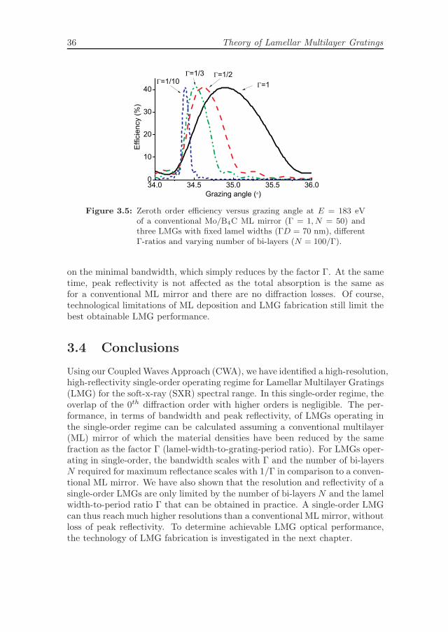
36 Theory of Lamellar Multilayer Gratings
Figure 3.5: Zeroth order efficiency versus grazing angle at E = 183 eVof a conventional Mo/B4C ML mirror (Γ = 1, N = 50) andthree LMGs with fixed lamel widths (ΓD = 70 nm), differentΓ-ratios and varying number of bi-layers (N = 100/Γ).
on the minimal bandwidth, which simply reduces by the factor Γ. At the sametime, peak reflectivity is not affected as the total absorption is the same asfor a conventional ML mirror and there are no diffraction losses. Of course,technological limitations of ML deposition and LMG fabrication still limit thebest obtainable LMG performance.
3.4 Conclusions
Using our CoupledWaves Approach (CWA), we have identified a high-resolution,high-reflectivity single-order operating regime for Lamellar Multilayer Gratings(LMG) for the soft-x-ray (SXR) spectral range. In this single-order regime, theoverlap of the 0th diffraction order with higher orders is negligible. The per-formance, in terms of bandwidth and peak reflectivity, of LMGs operating inthe single-order regime can be calculated assuming a conventional multilayer(ML) mirror of which the material densities have been reduced by the samefraction as the factor Γ (lamel-width-to-grating-period ratio). For LMGs oper-ating in single-order, the bandwidth scales with Γ and the number of bi-layersN required for maximum reflectance scales with 1/Γ in comparison to a conven-tional ML mirror. We have also shown that the resolution and reflectivity of asingle-order LMGs are only limited by the number of bi-layers N and the lamelwidth-to-period ratio Γ that can be obtained in practice. A single-order LMGcan thus reach much higher resolutions than a conventional ML mirror, withoutloss of peak reflectivity. To determine achievable LMG optical performance,the technology of LMG fabrication is investigated in the next chapter.

4Fabrication of gratings inW/Si multilayer mirrors
4.1 Introduction
The fabrication of single-order LMG structures requires the etching of nanoscalefeatures in ML mirrors. As EUV and soft x-ray wavelengths (figure 3.1a)are only a few nm, the ML stack has a bi-layer period d of comparable size.Furthermore, the bi-layers consist of two different materials that generally reactvery differently to the etching process. Due to the low refractive index contrast,the total ML stack generally consists of up to hundreds of bi-layers, resultingin total ML stack heights of ≥ 1 μm. For single-order LMG operation, therequired lamel aspect-ratios are in the order of ≥ 10:1, which is well abovepreviously achieved values of ∼ 5:1 [71]. As these structures are used as opticalelements, the fabrication should not negatively affect the optical behavior andconsequently leave the nanoscale layered arrangement intact.
Although Reactive Ion Etching (RIE) has been used to etch ML mirrors,this approach generally suffers from a lack of directional etching, resulting inpoor critical-dimension (CD) control and a limitation on ML stack heights thatcan be etched [63, 71]. Furthermore, these processes showed strong dependenceof the etch results on the grating structure. Although Bosch Deep Reactive IonEtching (Bosch DRIE) offers a directional pattern transfer, the cyclic nature ofBosch DRIE results in a typical sidewall scalloping of which the optical effectmay be unacceptable. Furthermore, the effect of the thin-layered structureswith dual-material composition, in particular the absorber layer, on etch resultsis unknown.
In this chapter, we demonstrate accurate and robust etching of W/Si ML
38 Fabrication of gratings in W/Si multilayer mirrors
mirrors for the fabrication of Lamellar Multilayer Gratings (LMG). For cost-effective fabrication of LMGs in small series, UV-NanoImprint Lithography wasused to define the grating structures. A Bosch DRIE process was developed totransfer this pattern into a ML stack. Using this process, we have reproduciblyfabricated LMGs with 200 nm grating periods and lamel aspect-ratios of∼ 17:1.The high aspect-ratio was achieved by using the layered structure of the ML.This layered structure suppressed scallop formation, which was subsequentlyused to achieve low tapers with minimal dependence on feature dimensions.
The experimental procedure is first discussed in section 4.2. Next, a descrip-tion of the Bosch etch process and scallop formation is given in section 4.3. Ageneralized Coupled Waves Approach was used to determine fabrication cri-teria for LMGs, as is presented in section 4.4. Finally, the effect of the MLlayered structure on etch results is investigated in section 4.5, where the mainfocus is on profile taper and scalloping.
4.2 Experimental
In this work, 400 mm silicon wafers were coated with 400 W/Si bi-layers (d-spacing of 2.53 nm and γ of 0.28) [72]. A single imprint template with 27 dif-ferent grating structures, having grating periods between 200 and 2000 nm andlamel widths between 60 and 1350 nm, was used to define various LMG struc-tures. This template was used for UV-NanoImprint Lithography (UV-NIL) inan Imprio 55 system from Molecular Imprints with the S-FILTM process [73].Before imprinting, a transfer layer of 60 nm DUV 30J was spincoated on theML wafer at 3000 rpm and then baked at 120 ◦C for 120 s. In the imprintmachine, a silicon containing imprint material was locally dispensed on top ofthe transfer layer. The template with the desired grating structures was thenpressed into the imprint material with a force of 3 N at room temperature.The imprint resist was cured by a 3 s UV exposure while the template was stillin contact. Finally, the template was detached leaving its negative shape inthe hardened imprint material. The patterned layer showed a feature heightof 100 nm and a residual layer of 40 nm [74]. Samples between 10x10 mm2
and 30x30 mm2 were then cleaved from the imprinted 400 mm ML wafer andan etch mask was prepared using a fluorine-based Reactive Ion Etching (RIE)process [74]. The sample was then fixed on a blank silicon carrier wafers usinga small droplet of FomblinTM vacuum oil for ML etching. All temperaturesused in the fabrication process were ≤ 120 ◦C to prevent annealing of the ML.This temperature was concluded to be acceptable as only a < 0.1% d-spacingchange was found in the ML after 60 hrs at this temperature as is discussed inmore detail in section 7.2.2.
For the ML etching, we used a fluorine based Bosch DRIE process in anAdixen Alcatel AMS100SE. This device has been described in detail in ref. [75].Such a process is feasible as both components of the multilayer react volatilewith fluorine [76–78]. To determine the ML etch process, the fabrication of
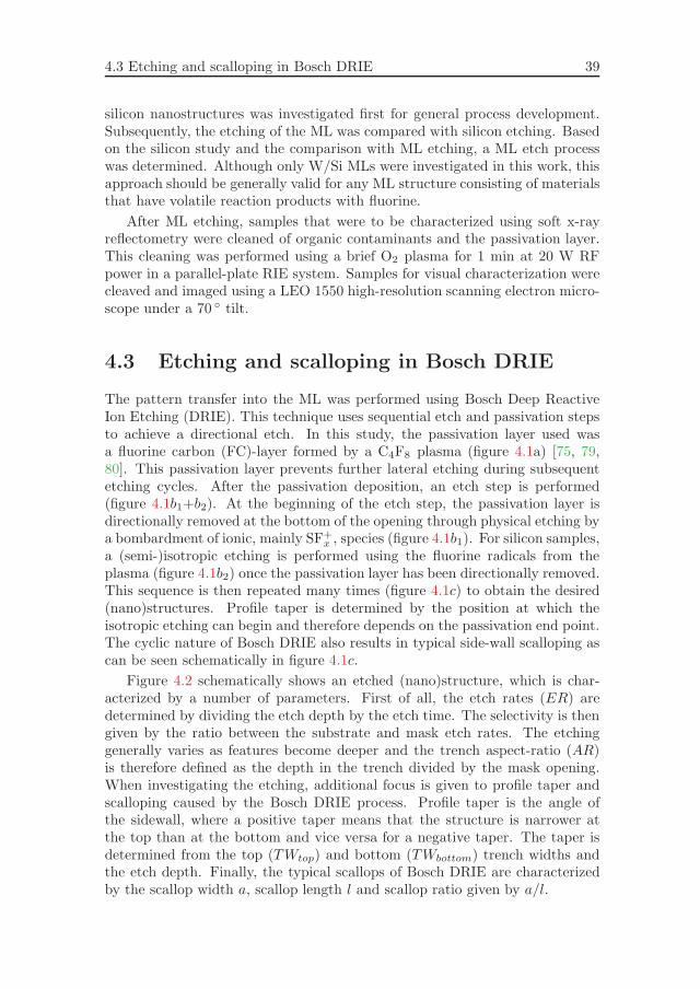
4.3 Etching and scalloping in Bosch DRIE 39
silicon nanostructures was investigated first for general process development.Subsequently, the etching of the ML was compared with silicon etching. Basedon the silicon study and the comparison with ML etching, a ML etch processwas determined. Although only W/Si MLs were investigated in this work, thisapproach should be generally valid for any ML structure consisting of materialsthat have volatile reaction products with fluorine.
After ML etching, samples that were to be characterized using soft x-rayreflectometry were cleaned of organic contaminants and the passivation layer.This cleaning was performed using a brief O2 plasma for 1 min at 20 W RFpower in a parallel-plate RIE system. Samples for visual characterization werecleaved and imaged using a LEO 1550 high-resolution scanning electron micro-scope under a 70 ◦ tilt.
4.3 Etching and scalloping in Bosch DRIE
The pattern transfer into the ML was performed using Bosch Deep ReactiveIon Etching (DRIE). This technique uses sequential etch and passivation stepsto achieve a directional etch. In this study, the passivation layer used wasa fluorine carbon (FC)-layer formed by a C4F8 plasma (figure 4.1a) [75, 79,80]. This passivation layer prevents further lateral etching during subsequentetching cycles. After the passivation deposition, an etch step is performed(figure 4.1b1+b2). At the beginning of the etch step, the passivation layer isdirectionally removed at the bottom of the opening through physical etching bya bombardment of ionic, mainly SF+
x , species (figure 4.1b1). For silicon samples,a (semi-)isotropic etching is performed using the fluorine radicals from theplasma (figure 4.1b2) once the passivation layer has been directionally removed.This sequence is then repeated many times (figure 4.1c) to obtain the desired(nano)structures. Profile taper is determined by the position at which theisotropic etching can begin and therefore depends on the passivation end point.The cyclic nature of Bosch DRIE also results in typical side-wall scalloping ascan be seen schematically in figure 4.1c.
Figure 4.2 schematically shows an etched (nano)structure, which is char-acterized by a number of parameters. First of all, the etch rates (ER) aredetermined by dividing the etch depth by the etch time. The selectivity is thengiven by the ratio between the substrate and mask etch rates. The etchinggenerally varies as features become deeper and the trench aspect-ratio (AR)is therefore defined as the depth in the trench divided by the mask opening.When investigating the etching, additional focus is given to profile taper andscalloping caused by the Bosch DRIE process. Profile taper is the angle ofthe sidewall, where a positive taper means that the structure is narrower atthe top than at the bottom and vice versa for a negative taper. The taper isdetermined from the top (TWtop) and bottom (TWbottom) trench widths andthe etch depth. Finally, the typical scallops of Bosch DRIE are characterizedby the scallop width a, scallop length l and scallop ratio given by a/l.
40 Fabrication of gratings in W/Si multilayer mirrors
Figure 4.1: Schematic of the various steps in Bosch DRIE. (a) A FC-passivation layer is deposited. (b1) At the beginning of theetch cycle, the passivation layer is partially removed by theincident ion flux with an energy and angular distributionN(E,α). (b2) As soon as the passivation layer is sufficientlyremoved, isotropic etching occurs. (c) Several passivation andetch cycles are performed to obtain a directional etch. Thepassivation end point is set by the removal of the passivationlayer (b1) and determines profile taper.
4.4 Determination of fabrication criteria
The pattern transfer into the ML inherently results in artifacts, such as sidewallscalloping, that were not considered in the LMG single-order derivation [5, 6](see also section 3.3). In order to understand the effects of such artifacts, wefirst briefly recall the operating principle of single-order LMGs. The bandwidthof conventional ML mirrors is determined by the number of bi-layers effectively(Neff ) contributing to the reflection. However, Neff is limited due to the highabsorption in the EUV and SXR spectral ranges. A reduction in absorptioncan be achieved by reducing the effective density, i.e. the lateral average per bi-layer, by fabricating a grating structure into the ML mirror. When operating in
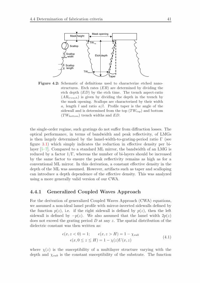
4.4 Determination of fabrication criteria 41
Figure 4.2: Schematic of definitions used to characterize etched nano-structures. Etch rates (ER) are determined by dividing theetch depth (ED) by the etch time. The trench aspect-ratio(ARtrench) is given by dividing the depth in the trench bythe mask opening. Scallops are characterized by their widtha, length l and ratio a/l. Profile taper is the angle of thesidewall and is determined from the top (TWtop) and bottom(TWbottom) trench widths and ED.
the single-order regime, such gratings do not suffer from diffraction losses. Theoptical performance, in terms of bandwidth and peak reflectivity, of LMGsis then largely determined by the lamel-width-to-grating-period ratio Γ (seefigure 3.1) which simply indicates the reduction in effective density per bi-layer [5–7]. Compared to a standard ML mirror, the bandwidth of an LMG isreduced by a factor 1/Γ, whereas the number of bi-layers should be increasedby the same factor to ensure the peak reflectivity remains as high as for aconventional ML mirror. In this derivation, a constant effective density in thedepth of the ML was assumed. However, artifacts such as taper and scallopingcan introduce a depth dependence of the effective density. This was analyzedusing a more generally valid version of our CWA.
4.4.1 Generalized Coupled Waves Approach
For the derivation of generalized Coupled Waves Approach (CWA) equations,we assumed a non-ideal lamel profile with mirror-inverted sidewalls defined bythe function p(z), i.e. if the right sidewall is defined by p(z), then the leftsidewall is defined by −p(z). We also assumed that the lamel width 2p(z)does not exceed the grating period D at any z. The spatial distribution of thedielectric constant was then written as:
ε(x, z < 0) = 1; ε(x, z > H) = 1− χsub
ε(x, 0 ≤ z ≤ H) = 1− χ(z)U(x, z)(4.1)
where χ(z) is the susceptibility of a multilayer structure varying with thedepth and χsub is the constant susceptibility of the substrate. The function
42 Fabrication of gratings in W/Si multilayer mirrors
U(x, z) = 1, if the point (x, z) is placed inside the multilayer structure andU = 0 otherwise.
Assuming the dielectric constant to be a periodic function of x, we repre-sented the function U as the Fourier series:
U(x, z) =
+∞∑n=−∞
Un(z)e2iπnx/D (4.2)
where
Un(z) =1
πnsin
(2πnp(z)
D
)(4.3)
with U0 = 2p(z)/D. Please note as in section 3.2.1 that eq. (4.3) differs tothat used in our previous works [5, 6] as the point x = 0 was now chosen to bein the center of the lamel instead of at the left side of the lamel. Shifting thecoordinates of the previous works by x′ = x−ΓD/2 yields the same coefficientsas used in this work.
Following the steps also used in ref. [5] and section 3.2, we eventually ob-tained an infinite system of coupled waves equations describing the amplitudesF of incident and reflected waves:
F′′n (z) + κ2
nFn(Z) = k2∑m
χ(z)Un−m(z)Fm(z) (4.4)
for n = 0,±1,±2, ... with boundary conditions:
F ′n(0) + iκnFn(0) = 2iκnδn,0; F ′
n(L)− iκ(s)n Fn(L) = 0 (4.5)
where κn =√k2 − q2n and κ
(s)n =
√k2εsub − q2n are the Z-components of the
wave vectors for the nth diffraction order in vacuum and the substrate, respec-tively, and δn,0 is the Kronecker symbol. The system (4.4)-(4.5) can be usedto simulate the optical effects of non-ideal lamel profiles, including taper andscalloping, by numerically solving this system as previously done in ref. [5] andsection 3.2.3.
For illustrative calculations in this work, we considered LMGs based onW/Si ML structures with parameters corresponding to those used in our exper-iments. The densities were taken to be ρW = 19 g/cm3 and ρSi = 2.35 g/cm3,bi-layer period d = 2.53 nm, absorber-to-bi-layer thickness ratio γ = 0.28 andwith N = 400 bi-layers. Interfacial roughness was not taken into account inthese calculations. The parameters of the grating were chosen to be a periodof D = 300 nm with a lamel-width-to-grating-period ratio Γ = 0.25 to ensuresingle-order operation.
4.4.2 Optical effect of tapering
To analyze the effect of a tapered lamel profile, we used the trapezoidal functionp(z) = DΓtop/2+D(Γbottom − Γtop)z/(2H) as shown in figure 4.3a to describe
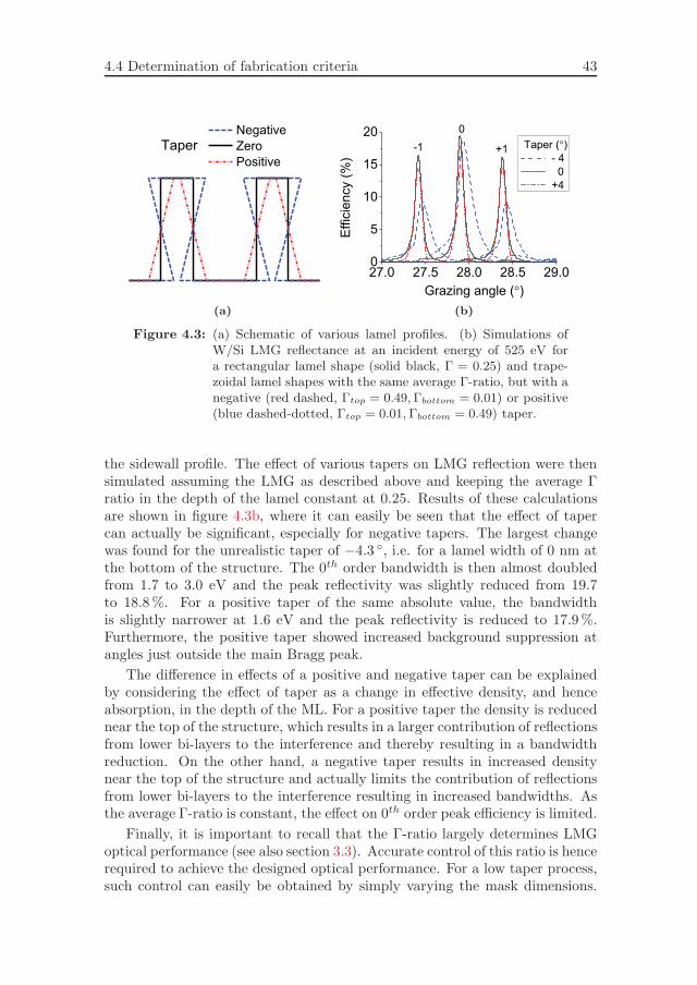
4.4 Determination of fabrication criteria 43
(a) (b)
Figure 4.3: (a) Schematic of various lamel profiles. (b) Simulations ofW/Si LMG reflectance at an incident energy of 525 eV fora rectangular lamel shape (solid black, Γ = 0.25) and trape-zoidal lamel shapes with the same average Γ-ratio, but with anegative (red dashed, Γtop = 0.49,Γbottom = 0.01) or positive(blue dashed-dotted, Γtop = 0.01, Γbottom = 0.49) taper.
the sidewall profile. The effect of various tapers on LMG reflection were thensimulated assuming the LMG as described above and keeping the average Γratio in the depth of the lamel constant at 0.25. Results of these calculationsare shown in figure 4.3b, where it can easily be seen that the effect of tapercan actually be significant, especially for negative tapers. The largest changewas found for the unrealistic taper of −4.3 ◦, i.e. for a lamel width of 0 nm atthe bottom of the structure. The 0th order bandwidth is then almost doubledfrom 1.7 to 3.0 eV and the peak reflectivity was slightly reduced from 19.7to 18.8%. For a positive taper of the same absolute value, the bandwidthis slightly narrower at 1.6 eV and the peak reflectivity is reduced to 17.9%.Furthermore, the positive taper showed increased background suppression atangles just outside the main Bragg peak.
The difference in effects of a positive and negative taper can be explainedby considering the effect of taper as a change in effective density, and henceabsorption, in the depth of the ML. For a positive taper the density is reducednear the top of the structure, which results in a larger contribution of reflectionsfrom lower bi-layers to the interference and thereby resulting in a bandwidthreduction. On the other hand, a negative taper results in increased densitynear the top of the structure and actually limits the contribution of reflectionsfrom lower bi-layers to the interference resulting in increased bandwidths. Asthe average Γ-ratio is constant, the effect on 0th order peak efficiency is limited.
Finally, it is important to recall that the Γ-ratio largely determines LMGoptical performance (see also section 3.3). Accurate control of this ratio is hencerequired to achieve the designed optical performance. For a low taper process,such control can easily be obtained by simply varying the mask dimensions.
44 Fabrication of gratings in W/Si multilayer mirrors
Hence, to ensure tapering does not affect the optical performance of LMGs,tapers should be limited to below±1 ◦, where slight positive tapers are preferredover negative ones.
4.4.3 Optical effect of scalloping
To analyze the effect of scalloping, the sidewall profile was described by the pe-riodic function p(z) = ΓD/2+a/2·sin(2πz/l). For single-order LMG operation,the effective susceptibility χeff (z) = χ(z) · 2p(z)/D is given by the product oftwo periodic functions with periods d and l. If the ratio d/l is an irrationalnumber, the function χeff (z) is not periodic. Expanding the functions χ(z)and p(z) into the Fourier series, we found that χeff (z) contains terms withfour main periods dj(j = 0 − 3), namely d0 = d, d1 = l, d2 = d/(1 + d/l) andd3 = d/(1 − d/l) as well as higher harmonics with periods dj/n(n = 2, 3, ...).As the scallop period l is typically much larger than the ML mirror period d0,reflection from this scallop period was not considered. However, the periods d2and d3 may be close to the ML mirror period d0 if the scallop length l is largeenough. A similar layered structure containing terms with different periodswas analyzed in details in ref. [81] as applied to the problem of simultaneousreflection of two arbitrary (not multiple) wavelengths from a multilayer mirror.
As for single-order operation (section 3.3), only the first order Bragg reflec-tion is of interest and higher order terms in the Fourier series are neglected. Thedepth-distribution of the effective susceptibility is then written in the simplifiedform:
χeff (z) ≈ Γχ+a
Dχ sin
(2πz
l
)+ (χA − χS)
sin(πγ)
π·[
2Γ cos
(2πz
d0− πγ
)+
a
Dsin
(2πz
d2− πγ
)− a
Dsin
(2πz
d3− πγ
)] (4.6)
If the grazing angle of the incident beam is varied, resonant Bragg reflec-
tion is observed from each of the three periods such that λ = 2dj sin(Θ(j)m=0),
where m = 0 indicates the 0th diffraction order and j = 0, 2, 3 is the in-dex of the period. The peak from j = 0 is the Bragg order, whereas j =2, 3 are peaks caused by scalloping and are referred to as scallop harmon-ics. Similarly, three diffraction peaks are also seen for any mth order such
that λ = 2dj
(sin(Θ
(j)m ) + sin(Φ
(j)m )
), where the periods dj are different and
the diffraction angle Φ(j)m , i.e. the grazing angle of the outgoing diffracted
beam, is determined by the grazing incidence angle via the grating equation
λ = D(cos(Θ
(j)m )− cos(Φ
(j)m )
). The optical effect of scalloping can therefore
be considered as the appearance of a phase grating in the depth of the MLstructure, which can be described by a number of embedded diffraction grat-
ings with the same D and Γ, but different ML periods dj . The angle Θ(j)m can
be referred to as the quasi-Bragg resonance angle and is comparable to the
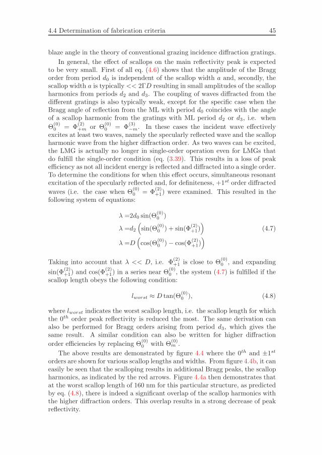
4.4 Determination of fabrication criteria 45
blaze angle in the theory of conventional grazing incidence diffraction gratings.
In general, the effect of scallops on the main reflectivity peak is expectedto be very small. First of all eq. (4.6) shows that the amplitude of the Braggorder from period d0 is independent of the scallop width a and, secondly, thescallop width a is typically << 2ΓD resulting in small amplitudes of the scallopharmonics from periods d2 and d3. The coupling of waves diffracted from thedifferent gratings is also typically weak, except for the specific case when theBragg angle of reflection from the ML with period d0 coincides with the angleof a scallop harmonic from the gratings with ML period d2 or d3, i.e. when
Θ(0)0 = Φ
(2)+m or Θ
(0)0 = Φ
(3)−m. In these cases the incident wave effectively
excites at least two waves, namely the specularly reflected wave and the scallopharmonic wave from the higher diffraction order. As two waves can be excited,the LMG is actually no longer in single-order operation even for LMGs thatdo fulfill the single-order condition (eq. (3.39). This results in a loss of peakefficiency as not all incident energy is reflected and diffracted into a single order.To determine the conditions for when this effect occurs, simultaneous resonantexcitation of the specularly reflected and, for definiteness, +1st order diffracted
waves (i.e. the case when Θ(0)0 = Φ
(2)+1) were examined. This resulted in the
following system of equations:
λ =2d0 sin(Θ(0)0 )
λ =d2
(sin(Θ
(0)0 ) + sin(Φ
(2)+1)
)(4.7)
λ =D(cos(Θ
(0)0 )− cos(Φ
(2)+1)
)
Taking into account that λ << D, i.e. Φ(2)+1 is close to Θ
(0)0 , and expanding
sin(Φ(2)+1) and cos(Φ
(2)+1) in a series near Θ
(0)0 , the system (4.7) is fulfilled if the
scallop length obeys the following condition:
lworst ≈ D tan(Θ(0)0 ), (4.8)
where lworst indicates the worst scallop length, i.e. the scallop length for whichthe 0th order peak reflectivity is reduced the most. The same derivation canalso be performed for Bragg orders arising from period d3, which gives thesame result. A similar condition can also be written for higher diffraction
order efficiencies by replacing Θ(0)0 with Θ
(0)m .
The above results are demonstrated by figure 4.4 where the 0th and ±1st
orders are shown for various scallop lengths and widths. From figure 4.4b, it caneasily be seen that the scalloping results in additional Bragg peaks, the scallopharmonics, as indicated by the red arrows. Figure 4.4a then demonstrates thatat the worst scallop length of 160 nm for this particular structure, as predictedby eq. (4.8), there is indeed a significant overlap of the scallop harmonics withthe higher diffraction orders. This overlap results in a strong decrease of peakreflectivity.
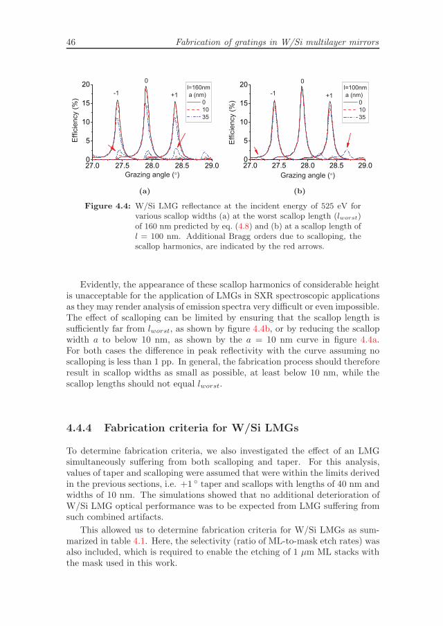
46 Fabrication of gratings in W/Si multilayer mirrors
(a) (b)
Figure 4.4: W/Si LMG reflectance at the incident energy of 525 eV forvarious scallop widths (a) at the worst scallop length (lworst)of 160 nm predicted by eq. (4.8) and (b) at a scallop length ofl = 100 nm. Additional Bragg orders due to scalloping, thescallop harmonics, are indicated by the red arrows.
Evidently, the appearance of these scallop harmonics of considerable heightis unacceptable for the application of LMGs in SXR spectroscopic applicationsas they may render analysis of emission spectra very difficult or even impossible.The effect of scalloping can be limited by ensuring that the scallop length issufficiently far from lworst, as shown by figure 4.4b, or by reducing the scallopwidth a to below 10 nm, as shown by the a = 10 nm curve in figure 4.4a.For both cases the difference in peak reflectivity with the curve assuming noscalloping is less than 1 pp. In general, the fabrication process should thereforeresult in scallop widths as small as possible, at least below 10 nm, while thescallop lengths should not equal lworst.
4.4.4 Fabrication criteria for W/Si LMGs
To determine fabrication criteria, we also investigated the effect of an LMGsimultaneously suffering from both scalloping and taper. For this analysis,values of taper and scalloping were assumed that were within the limits derivedin the previous sections, i.e. +1 ◦ taper and scallops with lengths of 40 nm andwidths of 10 nm. The simulations showed that no additional deterioration ofW/Si LMG optical performance was to be expected from LMG suffering fromsuch combined artifacts.
This allowed us to determine fabrication criteria for W/Si LMGs as sum-marized in table 4.1. Here, the selectivity (ratio of ML-to-mask etch rates) wasalso included, which is required to enable the etching of 1 μm ML stacks withthe mask used in this work.
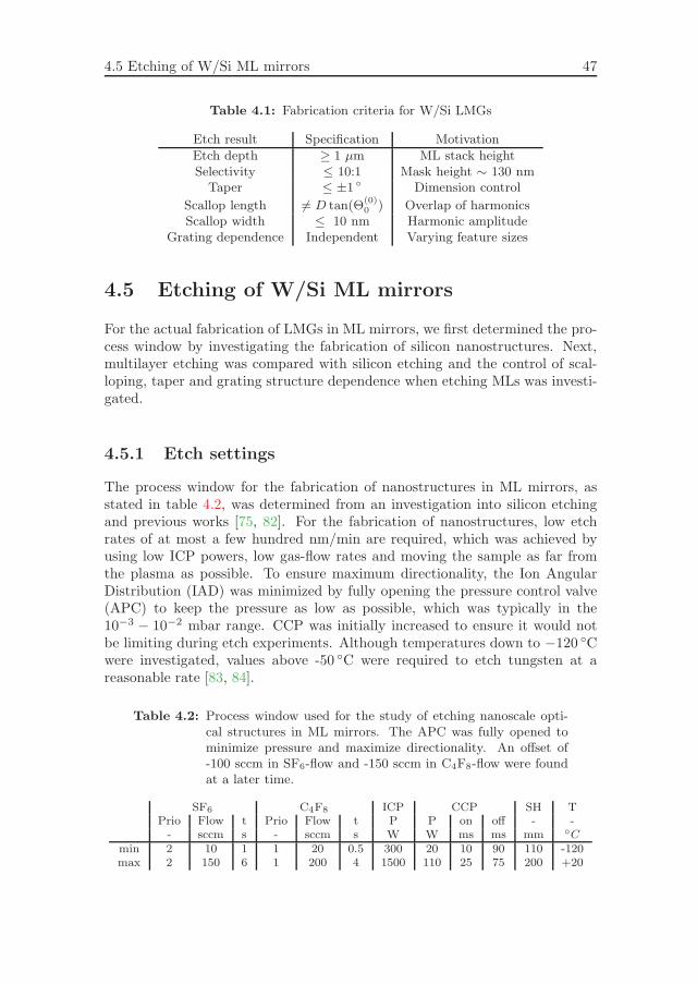
4.5 Etching of W/Si ML mirrors 47
Table 4.1: Fabrication criteria for W/Si LMGs
Etch result Specification Motivation
Etch depth ≥ 1 μm ML stack heightSelectivity ≤ 10:1 Mask height ∼ 130 nm
Taper ≤ ±1 ◦ Dimension control
Scallop length �= D tan(Θ(0)0 ) Overlap of harmonics
Scallop width ≤ 10 nm Harmonic amplitudeGrating dependence Independent Varying feature sizes
4.5 Etching of W/Si ML mirrors
For the actual fabrication of LMGs in ML mirrors, we first determined the pro-cess window by investigating the fabrication of silicon nanostructures. Next,multilayer etching was compared with silicon etching and the control of scal-loping, taper and grating structure dependence when etching MLs was investi-gated.
4.5.1 Etch settings
The process window for the fabrication of nanostructures in ML mirrors, asstated in table 4.2, was determined from an investigation into silicon etchingand previous works [75, 82]. For the fabrication of nanostructures, low etchrates of at most a few hundred nm/min are required, which was achieved byusing low ICP powers, low gas-flow rates and moving the sample as far fromthe plasma as possible. To ensure maximum directionality, the Ion AngularDistribution (IAD) was minimized by fully opening the pressure control valve(APC) to keep the pressure as low as possible, which was typically in the10−3 − 10−2 mbar range. CCP was initially increased to ensure it would notbe limiting during etch experiments. Although temperatures down to −120 ◦Cwere investigated, values above -50 ◦C were required to etch tungsten at areasonable rate [83, 84].
Table 4.2: Process window used for the study of etching nanoscale opti-cal structures in ML mirrors. The APC was fully opened tominimize pressure and maximize directionality. An offset of-100 sccm in SF6-flow and -150 sccm in C4F8-flow were foundat a later time.
SF6 C4F8 ICP CCP SH TPrio Flow t Prio Flow t P P on off - -- sccm s - sccm s W W ms ms mm ◦C
min 2 10 1 1 20 0.5 300 20 10 90 110 -120max 2 150 6 1 200 4 1500 110 25 75 200 +20
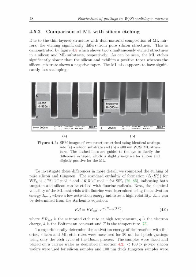
48 Fabrication of gratings in W/Si multilayer mirrors
4.5.2 Comparison of ML with silicon etching
Due to the thin-layered structure with dual-material composition of ML mir-rors, the etching significantly differs from pure silicon structures. This isdemonstrated by figure 4.5 which shows two simultaneously etched structuresin a silicon and ML substrate, respectively. As can be seen, the ML etchessignificantly slower than the silicon and exhibits a positive taper whereas thesilicon substrate shows a negative taper. The ML also appears to have signifi-cantly less scalloping.
(a) (b)
Figure 4.5: SEM images of two structures etched using identical settingsinto (a) a silicon substrate and (b) a 500 nm W/Si ML struc-ture. The dashed lines are guides to the eye to clarify thedifference in taper, which is slightly negative for silicon andslightly positive for the ML.
To investigate these differences in more detail, we compared the etching ofpure silicon and tungsten. The standard enthalpy of formation (ΔfH
0m) for
WF6 is -1721 kJ mol−1 and -1615 kJ mol−1 for SiF4 [76, 85], indicating bothtungsten and silicon can be etched with fluorine radicals. Next, the chemicalvolatility of the ML materials with fluorine was determined using the activationenergy Eact, where a low activation energy indicates a high volatility. Eact canbe determined from the Arrhenius equation:
ER = ERsat · e−qEact/(kT ), (4.9)
where ERsat is the saturated etch rate at high temperature, q is the electroncharge, k is the Boltzmann constant and T is the temperature [75].
To experimentally determine the activation energy of the reaction with flu-orine, silicon and ML etch rates were measured for 50 μm half pitch gratingsusing only the etch cycle of the Bosch process. The samples were diced andplaced on a carrier wafer as described in section 4.2. < 100 > p-type siliconwafers were used for silicon samples and 100 nm thick tungsten samples were
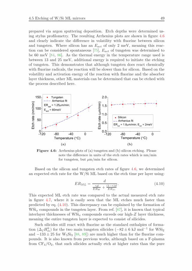
4.5 Etching of W/Si ML mirrors 49
prepared via argon sputtering deposition. Etch depths were determined us-ing stylus profilometry. The resulting Arrhenius plots are shown in figure 4.6and clearly indicate the difference in volatility with fluorine between siliconand tungsten. Where silicon has an Eact of only 2 meV, meaning this reac-tion can be considered spontaneous [75], Eact of tungsten was determined tobe 60 meV [84, 86]. As the thermal energy in the temperature range used isbetween 13 and 25 meV, additional energy is required to initiate the etchingof tungsten. This demonstrates that although tungsten does react chemicallywith fluorine radicals, the reaction will be slower than for silicon. Based on thevolatility and activation energy of the reaction with fluorine and the absorberlayer thickness, other ML materials can be determined that can be etched withthe process described here.
(a) (b)
Figure 4.6: Arrhenius plots of (a) tungsten and (b) silicon etching. Pleasenote the difference in units of the etch rates which is nm/minfor tungsten, but μm/min for silicon.
Based on the silicon and tungsten etch rates of figure 4.6, we determinedan expected etch rate for the W/Si ML based on the etch time per layer using:
ERML =d
γdERW
+ (1−γ)dERSi
. (4.10)
This expected ML etch rate was compared to the actual measured etch ratein figure 4.7, where it is easily seen that the ML etches much faster thanpredicted by eq. (4.10). This discrepancy can be explained by the formation ofWSix compounds in the tungsten layer. From ref. [87], it is known that typicalinterlayer thicknesses of WSix compounds exceeds our high-Z layer thickness,meaning the entire tungsten layer is expected to consist of silicides.
Such silicides still react with fluorine as the standard enthalpies of forma-tion (ΔfH
0m) for the two main tungsten silicides (−82± 6 kJ mol−1 for WSi2
and −133± 25 for W5Si3 [88, 89]) are much higher than for the fluorine com-pounds. It is also known from previous works, although based on a F-plasmafrom CF4/O2, that such silicides actually etch at higher rates than the pure
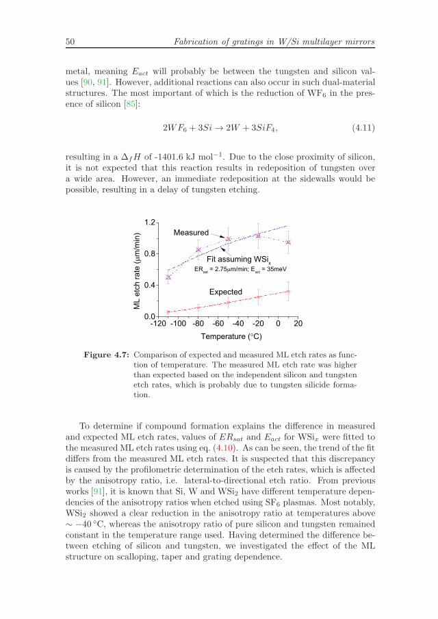
50 Fabrication of gratings in W/Si multilayer mirrors
metal, meaning Eact will probably be between the tungsten and silicon val-ues [90, 91]. However, additional reactions can also occur in such dual-materialstructures. The most important of which is the reduction of WF6 in the pres-ence of silicon [85]:
2WF6 + 3Si → 2W + 3SiF4, (4.11)
resulting in a ΔfH of -1401.6 kJ mol−1. Due to the close proximity of silicon,it is not expected that this reaction results in redeposition of tungsten overa wide area. However, an immediate redeposition at the sidewalls would bepossible, resulting in a delay of tungsten etching.
Figure 4.7: Comparison of expected and measured ML etch rates as func-tion of temperature. The measured ML etch rate was higherthan expected based on the independent silicon and tungstenetch rates, which is probably due to tungsten silicide forma-tion.
To determine if compound formation explains the difference in measuredand expected ML etch rates, values of ERsat and Eact for WSix were fitted tothe measured ML etch rates using eq. (4.10). As can be seen, the trend of the fitdiffers from the measured ML etch rates. It is suspected that this discrepancyis caused by the profilometric determination of the etch rates, which is affectedby the anisotropy ratio, i.e. lateral-to-directional etch ratio. From previousworks [91], it is known that Si, W and WSi2 have different temperature depen-dencies of the anisotropy ratios when etched using SF6 plasmas. Most notably,WSi2 showed a clear reduction in the anisotropy ratio at temperatures above∼ −40 ◦C, whereas the anisotropy ratio of pure silicon and tungsten remainedconstant in the temperature range used. Having determined the difference be-tween etching of silicon and tungsten, we investigated the effect of the MLstructure on scalloping, taper and grating dependence.
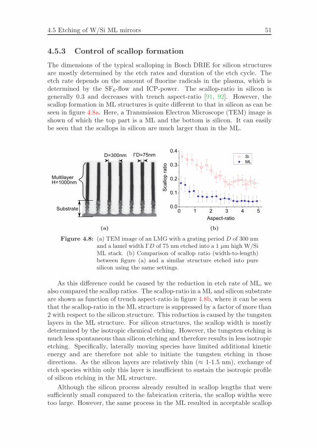
4.5 Etching of W/Si ML mirrors 51
4.5.3 Control of scallop formation
The dimensions of the typical scalloping in Bosch DRIE for silicon structuresare mostly determined by the etch rates and duration of the etch cycle. Theetch rate depends on the amount of fluorine radicals in the plasma, which isdetermined by the SF6-flow and ICP-power. The scallop-ratio in silicon isgenerally 0.3 and decreases with trench aspect-ratio [91, 92]. However, thescallop formation in ML structures is quite different to that in silicon as can beseen in figure 4.8a. Here, a Transmission Electron Microscope (TEM) image isshown of which the top part is a ML and the bottom is silicon. It can easilybe seen that the scallops in silicon are much larger than in the ML.
(a) (b)
Figure 4.8: (a) TEM image of an LMG with a grating period D of 300 nmand a lamel width ΓD of 75 nm etched into a 1 μm high W/SiML stack. (b) Comparison of scallop ratio (width-to-length)between figure (a) and a similar structure etched into puresilicon using the same settings.
As this difference could be caused by the reduction in etch rate of ML, wealso compared the scallop ratios. The scallop-ratio in a ML and silicon substrateare shown as function of trench aspect-ratio in figure 4.8b, where it can be seenthat the scallop-ratio in the ML structure is suppressed by a factor of more than2 with respect to the silicon structure. This reduction is caused by the tungstenlayers in the ML structure. For silicon structures, the scallop width is mostlydetermined by the isotropic chemical etching. However, the tungsten etching ismuch less spontaneous than silicon etching and therefore results in less isotropicetching. Specifically, laterally moving species have limited additional kineticenergy and are therefore not able to initiate the tungsten etching in thosedirections. As the silicon layers are relatively thin (≈ 1-1.5 nm), exchange ofetch species within only this layer is insufficient to sustain the isotropic profileof silicon etching in the ML structure.
Although the silicon process already resulted in scallop lengths that weresufficiently small compared to the fabrication criteria, the scallop widths weretoo large. However, the same process in the ML resulted in acceptable scallop
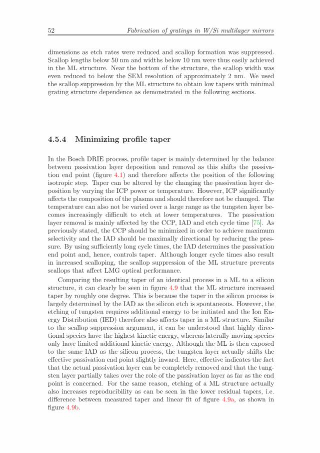
52 Fabrication of gratings in W/Si multilayer mirrors
dimensions as etch rates were reduced and scallop formation was suppressed.Scallop lengths below 50 nm and widths below 10 nm were thus easily achievedin the ML structure. Near the bottom of the structure, the scallop width waseven reduced to below the SEM resolution of approximately 2 nm. We usedthe scallop suppression by the ML structure to obtain low tapers with minimalgrating structure dependence as demonstrated in the following sections.
4.5.4 Minimizing profile taper
In the Bosch DRIE process, profile taper is mainly determined by the balancebetween passivation layer deposition and removal as this shifts the passiva-tion end point (figure 4.1) and therefore affects the position of the followingisotropic step. Taper can be altered by the changing the passivation layer de-position by varying the ICP power or temperature. However, ICP significantlyaffects the composition of the plasma and should therefore not be changed. Thetemperature can also not be varied over a large range as the tungsten layer be-comes increasingly difficult to etch at lower temperatures. The passivationlayer removal is mainly affected by the CCP, IAD and etch cycle time [75]. Aspreviously stated, the CCP should be minimized in order to achieve maximumselectivity and the IAD should be maximally directional by reducing the pres-sure. By using sufficiently long cycle times, the IAD determines the passivationend point and, hence, controls taper. Although longer cycle times also resultin increased scalloping, the scallop suppression of the ML structure preventsscallops that affect LMG optical performance.
Comparing the resulting taper of an identical process in a ML to a siliconstructure, it can clearly be seen in figure 4.9 that the ML structure increasedtaper by roughly one degree. This is because the taper in the silicon process islargely determined by the IAD as the silicon etch is spontaneous. However, theetching of tungsten requires additional energy to be initiated and the Ion En-ergy Distribution (IED) therefore also affects taper in a ML structure. Similarto the scallop suppression argument, it can be understood that highly direc-tional species have the highest kinetic energy, whereas laterally moving speciesonly have limited additional kinetic energy. Although the ML is then exposedto the same IAD as the silicon process, the tungsten layer actually shifts theeffective passivation end point slightly inward. Here, effective indicates the factthat the actual passivation layer can be completely removed and that the tung-sten layer partially takes over the role of the passivation layer as far as the endpoint is concerned. For the same reason, etching of a ML structure actuallyalso increases reproducibility as can be seen in the lower residual tapers, i.e.difference between measured taper and linear fit of figure 4.9a, as shown infigure 4.9b.
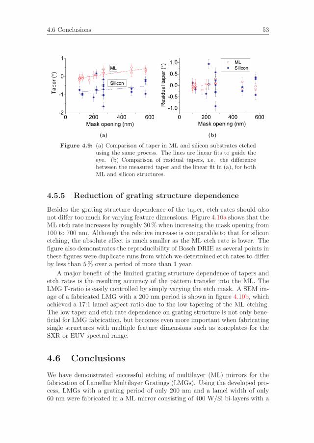
4.6 Conclusions 53
(a) (b)
Figure 4.9: (a) Comparison of taper in ML and silicon substrates etchedusing the same process. The lines are linear fits to guide theeye. (b) Comparison of residual tapers, i.e. the differencebetween the measured taper and the linear fit in (a), for bothML and silicon structures.
4.5.5 Reduction of grating structure dependence
Besides the grating structure dependence of the taper, etch rates should alsonot differ too much for varying feature dimensions. Figure 4.10a shows that theML etch rate increases by roughly 30% when increasing the mask opening from100 to 700 nm. Although the relative increase is comparable to that for siliconetching, the absolute effect is much smaller as the ML etch rate is lower. Thefigure also demonstrates the reproducibility of Bosch DRIE as several points inthese figures were duplicate runs from which we determined etch rates to differby less than 5% over a period of more than 1 year.
A major benefit of the limited grating structure dependence of tapers andetch rates is the resulting accuracy of the pattern transfer into the ML. TheLMG Γ-ratio is easily controlled by simply varying the etch mask. A SEM im-age of a fabricated LMG with a 200 nm period is shown in figure 4.10b, whichachieved a 17:1 lamel aspect-ratio due to the low tapering of the ML etching.The low taper and etch rate dependence on grating structure is not only bene-ficial for LMG fabrication, but becomes even more important when fabricatingsingle structures with multiple feature dimensions such as zoneplates for theSXR or EUV spectral range.
4.6 Conclusions
We have demonstrated successful etching of multilayer (ML) mirrors for thefabrication of Lamellar Multilayer Gratings (LMGs). Using the developed pro-cess, LMGs with a grating period of only 200 nm and a lamel width of only60 nm were fabricated in a ML mirror consisting of 400 W/Si bi-layers with a
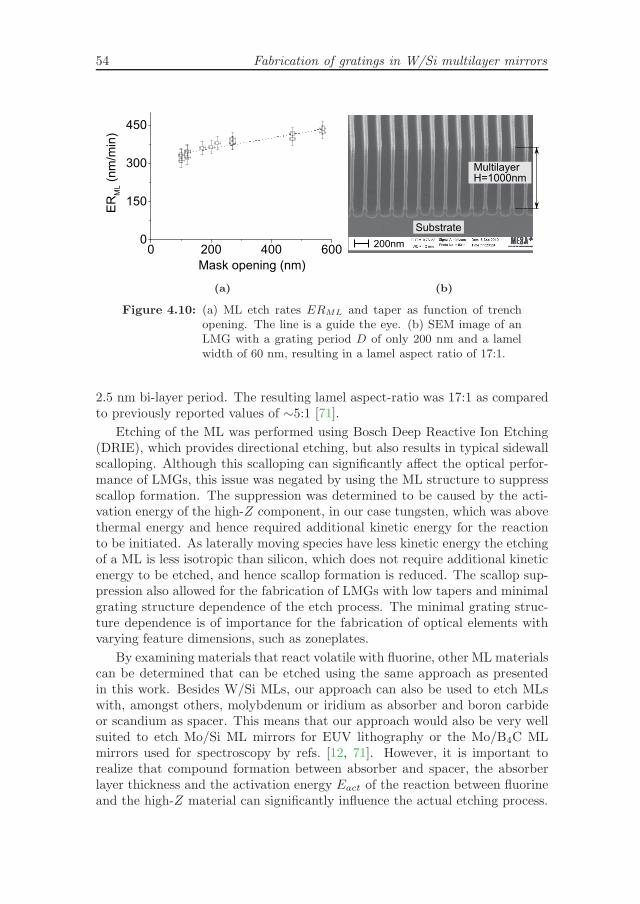
54 Fabrication of gratings in W/Si multilayer mirrors
(a) (b)
Figure 4.10: (a) ML etch rates ERML and taper as function of trenchopening. The line is a guide the eye. (b) SEM image of anLMG with a grating period D of only 200 nm and a lamelwidth of 60 nm, resulting in a lamel aspect ratio of 17:1.
2.5 nm bi-layer period. The resulting lamel aspect-ratio was 17:1 as comparedto previously reported values of ∼5:1 [71].
Etching of the ML was performed using Bosch Deep Reactive Ion Etching(DRIE), which provides directional etching, but also results in typical sidewallscalloping. Although this scalloping can significantly affect the optical perfor-mance of LMGs, this issue was negated by using the ML structure to suppressscallop formation. The suppression was determined to be caused by the acti-vation energy of the high-Z component, in our case tungsten, which was abovethermal energy and hence required additional kinetic energy for the reactionto be initiated. As laterally moving species have less kinetic energy the etchingof a ML is less isotropic than silicon, which does not require additional kineticenergy to be etched, and hence scallop formation is reduced. The scallop sup-pression also allowed for the fabrication of LMGs with low tapers and minimalgrating structure dependence of the etch process. The minimal grating struc-ture dependence is of importance for the fabrication of optical elements withvarying feature dimensions, such as zoneplates.
By examining materials that react volatile with fluorine, other ML materialscan be determined that can be etched using the same approach as presentedin this work. Besides W/Si MLs, our approach can also be used to etch MLswith, amongst others, molybdenum or iridium as absorber and boron carbideor scandium as spacer. This means that our approach would also be very wellsuited to etch Mo/Si ML mirrors for EUV lithography or the Mo/B4C MLmirrors used for spectroscopy by refs. [12, 71]. However, it is important torealize that compound formation between absorber and spacer, the absorberlayer thickness and the activation energy Eact of the reaction between fluorineand the high-Z material can significantly influence the actual etching process.
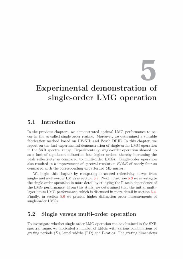
5Experimental demonstration of
single-order LMG operation
5.1 Introduction
In the previous chapters, we demonstrated optimal LMG performance to oc-cur in the so-called single-order regime. Moreover, we determined a suitablefabrication method based on UV-NIL and Bosch DRIE. In this chapter, wereport on the first experimental demonstration of single-order LMG operationin the SXR spectral range. Experimentally, single-order operation showed upas a lack of significant diffraction into higher orders, thereby increasing thepeak reflectivity as compared to multi-order LMGs. Single-order operationalso resulted in a improvement of spectral resolution E/ΔE of nearly four ascompared with the corresponding unpatterned ML mirror.
We begin this chapter by comparing measured reflectivity curves fromsingle- and multi-order LMGs in section 5.2. Next, in section 5.3 we investigatethe single-order operation in more detail by studying the Γ-ratio dependence ofthe LMG performance. From this study, we determined that the initial multi-layer limits LMG performance, which is discussed in more detail in section 5.4.Finally, in section 5.6 we present higher diffraction order measurements ofsingle-order LMGs.
5.2 Single versus multi-order operation
To investigate whether single-order LMG operation can be obtained in the SXRspectral range, we fabricated a number of LMGs with various combinations ofgrating periods (D), lamel widths (ΓD) and Γ-ratios. The grating dimensions
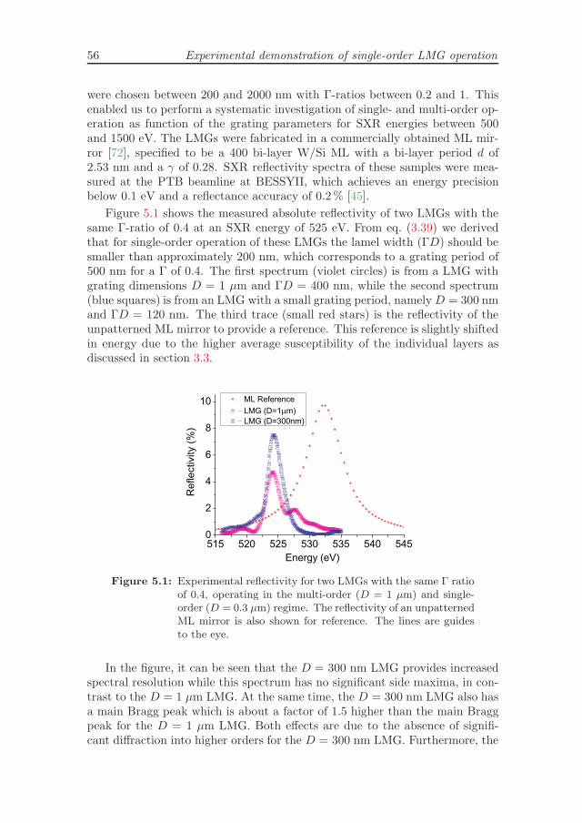
56 Experimental demonstration of single-order LMG operation
were chosen between 200 and 2000 nm with Γ-ratios between 0.2 and 1. Thisenabled us to perform a systematic investigation of single- and multi-order op-eration as function of the grating parameters for SXR energies between 500and 1500 eV. The LMGs were fabricated in a commercially obtained ML mir-ror [72], specified to be a 400 bi-layer W/Si ML with a bi-layer period d of2.53 nm and a γ of 0.28. SXR reflectivity spectra of these samples were mea-sured at the PTB beamline at BESSYII, which achieves an energy precisionbelow 0.1 eV and a reflectance accuracy of 0.2% [45].
Figure 5.1 shows the measured absolute reflectivity of two LMGs with thesame Γ-ratio of 0.4 at an SXR energy of 525 eV. From eq. (3.39) we derivedthat for single-order operation of these LMGs the lamel width (ΓD) should besmaller than approximately 200 nm, which corresponds to a grating period of500 nm for a Γ of 0.4. The first spectrum (violet circles) is from a LMG withgrating dimensions D = 1 μm and ΓD = 400 nm, while the second spectrum(blue squares) is from an LMG with a small grating period, namelyD = 300 nmand ΓD = 120 nm. The third trace (small red stars) is the reflectivity of theunpatterned ML mirror to provide a reference. This reference is slightly shiftedin energy due to the higher average susceptibility of the individual layers asdiscussed in section 3.3.
Figure 5.1: Experimental reflectivity for two LMGs with the same Γ ratioof 0.4, operating in the multi-order (D = 1 μm) and single-order (D = 0.3 μm) regime. The reflectivity of an unpatternedML mirror is also shown for reference. The lines are guidesto the eye.
In the figure, it can be seen that the D = 300 nm LMG provides increasedspectral resolution while this spectrum has no significant side maxima, in con-trast to the D = 1 μm LMG. At the same time, the D = 300 nm LMG also hasa main Bragg peak which is about a factor of 1.5 higher than the main Braggpeak for the D = 1 μm LMG. Both effects are due to the absence of signifi-cant diffraction into higher orders for the D = 300 nm LMG. Furthermore, the
5.3 Single-order Γ scaling 57
FWHM bandwidth of the D = 300 nm LMG is a factor of 2.5 narrower thanthat of the reference spectrum, which is in agreement with the 1/Γ bandwidthscaling predicted for single-order operating LMGs in section 3.3 [5].
These observations prove that single-order LMG operation can be achievedin the SXR spectral range. The largest resolution improvement, also obtainedwith a single-order operating LMG around 525 eV, had a factor 3.8 narrowerbandwidth (1.85 eV) than that of the unpatterned ML mirror (7.02 eV).
5.3 Single-order Γ scaling
For a more systematic analysis of spectral narrowing in single-order LMG oper-ation, we extended our experiments with reflectivity measurements at a higherphoton energy (E = 1255 eV) where more LMGs can be operated in single-orderfor a broader range of Γ values (0.2 to 0.8). The measured spectral bandwidthsand peak reflectivities are shown in figure 5.2 as a function of Γ. It can beseen in figure 5.2a that the spectral bandwidth of the LMG decreases with de-creasing Γ, showing a factor 3.3 improvement in spectral resolution when goingfrom the unpatterned ML mirror (Γ = 1) to an LMG with Γ = 0.22. At thesame time, it can be seen from figure 5.2b that the peak reflectivity decreasesfor lower Γ-ratios and drops to approximately half of its initial value at Γ =0.2.
(a) (b)
Figure 5.2: (a) FWHM and (b) peak reflectivity for several single-orderLMGs at the SXR energy of 1255 eV. Results of calculationsusing our theoretical model including the measured bi-layerchirp are in good agreement with the measured data.
We compared the experimental data with theoretical calculations of thespectral bandwidths and peak reflectivities as function of Γ using our CoupledWaves Approach (CWA) as derived in section 3.2. In these calculations, weincluded various effects usually found in ML mirrors, such as rms interlayerroughness (σ) and interface width (w). By fitting the calculations to the mea-
58 Experimental demonstration of single-order LMG operation
sured spectra of the unpatterned ML mirror recorded at various energies andtaking the finite number of bi-layers (N = 400) into account, values of d =2.53 nm, γ = 0.25, σ = 0.29 nm and w = 0.42 nm were obtained. Thesecalculations are shown in figure 5.2 as “constant d” . As can be seen, thesesimulations do not agree well with the measurements. In particular, the peakreflectivity at lower Γ-ratio’s is well below the theoretical value.
Possible factors that decrease the peak reflectivity of a ML mirror and,hence, that of a single-order operating LMG can be: (a) interfacial roughness,(b) interlayer formation and interdiffusion between neighboring materials and(c) random or deterministic variation of layer thickness both in the depth andalong the ML surface. Although we could not exclude that the etching ofthe ML stack may result in increased interfacial roughness or interlayer forma-tion, neither photo-electron spectroscopy data nor high-resolution transmissionelectron microscopy images indicated any difference between the ML stacks be-fore and after etching. Increased roughness and interlayer formation also onlyreduce peak reflectivity without increasing the bandwidth. In contrary, simu-lations showed that bi-layer period variations can reduce the peak reflectivityand simultaneously result in increased reflectivity bandwidths.
5.4 Bi-layer period accuracy
As an independent check for the degree of bi-layer periodicity, we recordedreflectivity spectra from the Total External Reflection region up to the 4th
Bragg order of the unpatterned ML mirror at the hard x-ray energy of 8 keV(HXR). In figure 5.3, the normalized 2nd Bragg order is shown and comparedto calculations revealing a slight (0.5%) linear increase (chirp) of the bi-layerperiod d in the depth of the ML stack. Calculations of the SXR spectralbandwidths and peak reflectivities including the measured chirp are shown infigure 5.2 as “chirped d” and can be seen to agree with the measured data towithin a few relative percent. The discrepancy in peak reflectivity between the“chirped d” simulations and the reference measurement (Γ = 1) is believed tobe caused by sidewall effects that only occur in the LMGs. The reference wasactually on the same sample as the LMGs and, as it was exposed to identicalfabrication steps as the LMGs, fabrication can largely be excluded as cause forthis difference.
Although the bi-layer chirp in the ML stack was not limiting for use as aconventional ML mirror, LMGs require increased accuracies as the SXR pene-tration depth is increased and the reflected waves thus need to constructivelyinterfere within a narrower bandwidth. To ensure bi-layer period variationsΔd/d do not affect LMG performance, they should not exceed ΔE/E ≈ 1/Neff
(see ref. [18]) and refs. therein), leading to the bi-layer period accuracy condi-tion:
ΔdLMG ≤ ΔdMMΓ (5.1)
where ΔdLMG and ΔdMM are the tolerable variations in bi-layer period for
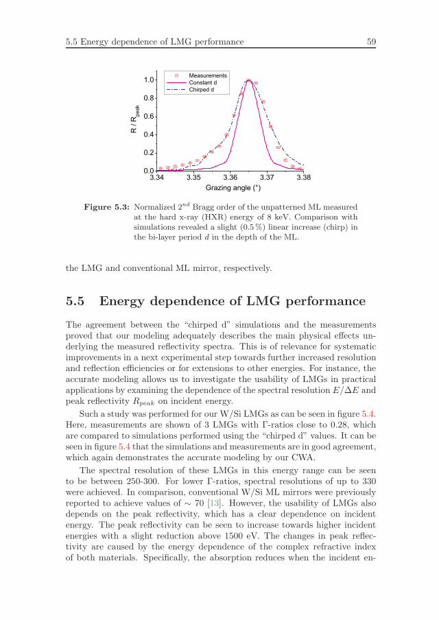
5.5 Energy dependence of LMG performance 59
Figure 5.3: Normalized 2nd Bragg order of the unpatterned ML measuredat the hard x-ray (HXR) energy of 8 keV. Comparison withsimulations revealed a slight (0.5%) linear increase (chirp) inthe bi-layer period d in the depth of the ML.
the LMG and conventional ML mirror, respectively.
5.5 Energy dependence of LMG performance
The agreement between the “chirped d” simulations and the measurementsproved that our modeling adequately describes the main physical effects un-derlying the measured reflectivity spectra. This is of relevance for systematicimprovements in a next experimental step towards further increased resolutionand reflection efficiencies or for extensions to other energies. For instance, theaccurate modeling allows us to investigate the usability of LMGs in practicalapplications by examining the dependence of the spectral resolution E/ΔE andpeak reflectivity Rpeak on incident energy.
Such a study was performed for our W/Si LMGs as can be seen in figure 5.4.Here, measurements are shown of 3 LMGs with Γ-ratios close to 0.28, whichare compared to simulations performed using the “chirped d” values. It can beseen in figure 5.4 that the simulations and measurements are in good agreement,which again demonstrates the accurate modeling by our CWA.
The spectral resolution of these LMGs in this energy range can be seento be between 250-300. For lower Γ-ratios, spectral resolutions of up to 330were achieved. In comparison, conventional W/Si ML mirrors were previouslyreported to achieve values of ∼ 70 [13]. However, the usability of LMGs alsodepends on the peak reflectivity, which has a clear dependence on incidentenergy. The peak reflectivity can be seen to increase towards higher incidentenergies with a slight reduction above 1500 eV. The changes in peak reflec-tivity are caused by the energy dependence of the complex refractive indexof both materials. Specifically, the absorption reduces when the incident en-
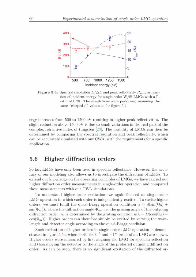
60 Experimental demonstration of single-order LMG operation
Figure 5.4: Spectral resolution E/ΔE and peak reflectivity Rpeak as func-tion of incident energy for single-order W/Si LMGs with a Γ-ratio of 0.28. The simulations were performed assuming thesame “chirped d” values as for figure 5.2.
ergy increases from 500 to 1500 eV resulting in higher peak reflectivities. Theslight reduction above 1500 eV is due to small variations in the real part of thecomplex refractive index of tungsten [23]. The usability of LMGs can then bedetermined by comparing the spectral resolution and peak reflectivity, whichcan be accurately simulated with our CWA, with the requirements for a specificapplication.
5.6 Higher diffraction orders
So far, LMGs have only been used in specular reflectance. However, the accu-racy of our modeling also allows us to investigate the diffraction of LMGs. Toextend our knowledge on the operating principles of LMGs, we have carried outhigher diffraction order measurements in single-order operation and comparedthese measurements with our CWA simulations.
To understand higher order excitation, we again focused on single-orderLMG operation in which each order is independently excited. To excite higherorders, we must fulfill the quasi-Bragg operation condition λ ≈ d(sin(Θ0) +sin(Φm)), where the diffraction angle Φm, i.e. the grazing angle of the outgoingdiffraction order m, is determined by the grating equation mλ = D(cos(Θ0)−cos(Φm)). Higher orders can therefore simply be excited by varying the wave-length and detector angle according to the quasi-Bragg condition.
Such excitation of higher orders in single-order LMG operation is demon-strated in figure 5.5a, where both the 0th and −1st order of an LMG are shown.Higher orders were measured by first aligning the LMG for specular reflectionand then moving the detector to the angle of the preferred outgoing diffractionorder. As can be seen, there is no significant excitation of the diffracted or-
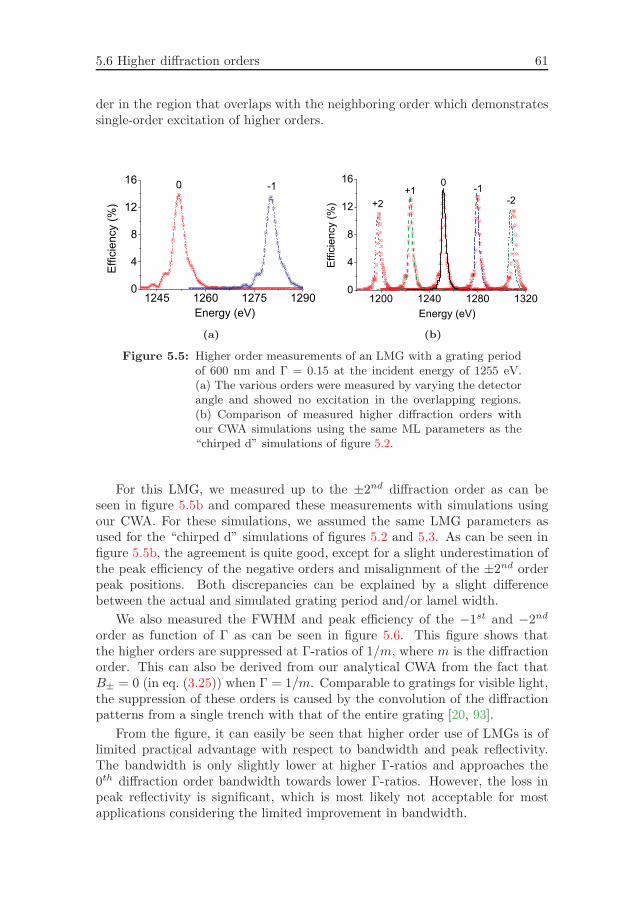
5.6 Higher diffraction orders 61
der in the region that overlaps with the neighboring order which demonstratessingle-order excitation of higher orders.
(a) (b)
Figure 5.5: Higher order measurements of an LMG with a grating periodof 600 nm and Γ = 0.15 at the incident energy of 1255 eV.(a) The various orders were measured by varying the detectorangle and showed no excitation in the overlapping regions.(b) Comparison of measured higher diffraction orders withour CWA simulations using the same ML parameters as the“chirped d” simulations of figure 5.2.
For this LMG, we measured up to the ±2nd diffraction order as can beseen in figure 5.5b and compared these measurements with simulations usingour CWA. For these simulations, we assumed the same LMG parameters asused for the “chirped d” simulations of figures 5.2 and 5.3. As can be seen infigure 5.5b, the agreement is quite good, except for a slight underestimation ofthe peak efficiency of the negative orders and misalignment of the ±2nd orderpeak positions. Both discrepancies can be explained by a slight differencebetween the actual and simulated grating period and/or lamel width.
We also measured the FWHM and peak efficiency of the −1st and −2nd
order as function of Γ as can be seen in figure 5.6. This figure shows thatthe higher orders are suppressed at Γ-ratios of 1/m, where m is the diffractionorder. This can also be derived from our analytical CWA from the fact thatB± = 0 (in eq. (3.25)) when Γ = 1/m. Comparable to gratings for visible light,the suppression of these orders is caused by the convolution of the diffractionpatterns from a single trench with that of the entire grating [20, 93].
From the figure, it can easily be seen that higher order use of LMGs is oflimited practical advantage with respect to bandwidth and peak reflectivity.The bandwidth is only slightly lower at higher Γ-ratios and approaches the0th diffraction order bandwidth towards lower Γ-ratios. However, the loss inpeak reflectivity is significant, which is most likely not acceptable for mostapplications considering the limited improvement in bandwidth.
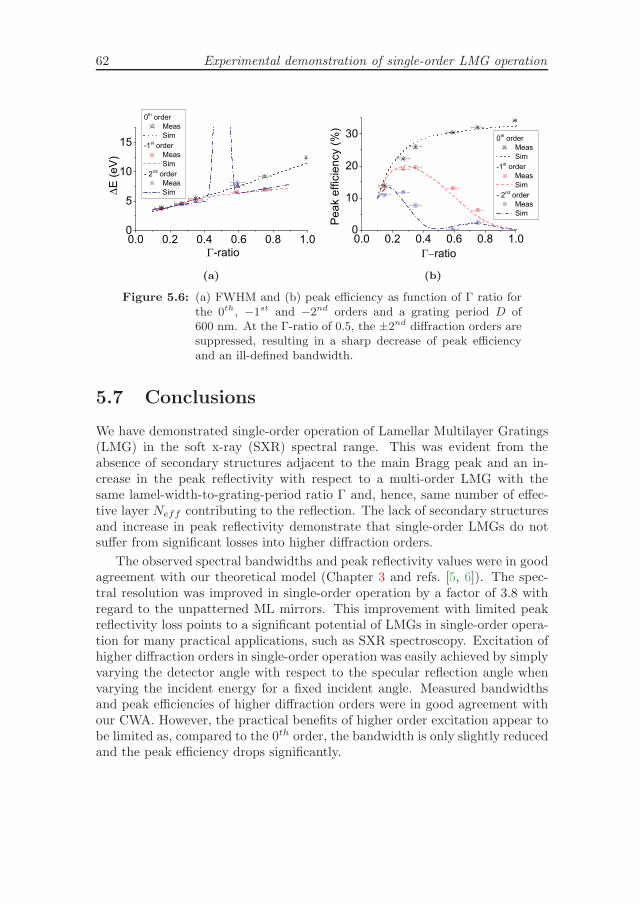
62 Experimental demonstration of single-order LMG operation
(a) (b)
Figure 5.6: (a) FWHM and (b) peak efficiency as function of Γ ratio forthe 0th, −1st and −2nd orders and a grating period D of600 nm. At the Γ-ratio of 0.5, the ±2nd diffraction orders aresuppressed, resulting in a sharp decrease of peak efficiencyand an ill-defined bandwidth.
5.7 Conclusions
We have demonstrated single-order operation of Lamellar Multilayer Gratings(LMG) in the soft x-ray (SXR) spectral range. This was evident from theabsence of secondary structures adjacent to the main Bragg peak and an in-crease in the peak reflectivity with respect to a multi-order LMG with thesame lamel-width-to-grating-period ratio Γ and, hence, same number of effec-tive layer Neff contributing to the reflection. The lack of secondary structuresand increase in peak reflectivity demonstrate that single-order LMGs do notsuffer from significant losses into higher diffraction orders.
The observed spectral bandwidths and peak reflectivity values were in goodagreement with our theoretical model (Chapter 3 and refs. [5, 6]). The spec-tral resolution was improved in single-order operation by a factor of 3.8 withregard to the unpatterned ML mirrors. This improvement with limited peakreflectivity loss points to a significant potential of LMGs in single-order opera-tion for many practical applications, such as SXR spectroscopy. Excitation ofhigher diffraction orders in single-order operation was easily achieved by simplyvarying the detector angle with respect to the specular reflection angle whenvarying the incident energy for a fixed incident angle. Measured bandwidthsand peak efficiencies of higher diffraction orders were in good agreement withour CWA. However, the practical benefits of higher order excitation appear tobe limited as, compared to the 0th order, the bandwidth is only slightly reducedand the peak efficiency drops significantly.
6Performance of finite stack
Lamellar Multilayer Gratings
6.1 Introduction
The spectral resolution of multilayer (ML) mirrors for the soft x-ray (SXR)spectral range can be improved by fabricating a grating into such a mirror.The resulting structure is referred to as a Lamellar Multilayer Grating (LMG).Design of LMGs has previously always assumed the idealized case of a semi-infinite ML stack, where the ML and grating parameters were considered in-dependently. The ML would be designed first following Refs. [4, 67] and theeffect of the grating would then be considered subsequently. The effect of thegrating on LMG optical performance, in terms of bandwidth and peak reflec-tivity, can be easily predicted for LMGs operating in single-order, i.e. whenthe incident wave only excites a single diffraction order. The bandwidth thennamely simply scales with the lamel-width-to-grating-period ratio Γ and thepeak reflectivity can be as high as that of a conventional ML mirror. However,this requires an increase in both the number of bi-layers and the accuracy ofthe deposited bi-layer period by 1/Γ as compared to conventional ML mirrorsto fulfill the semi-infinite ML approximation [5–7, 74].
The semi-infinite ML approximation generally requires ML stacks of severalμm height that consist of hundreds or even thousands of bi-layers that need tobe deposited with sub-pm accuracy [5, 7]. Furthermore, gratings then need tobe fabricated into these ML stacks with lamel widths in the order of 100 nm andsub-μm grating periods [74]. Such structures can usually not be deposited orfabricated with sufficient accuracy using current technologies. As a result, mostLMGs are fabricated in ML stacks with insufficient bi-layers to fully reflect theincident beam, i.e. part of the incident beam extends into the substrate. This
64 Performance of finite stack Lamellar Multilayer Gratings
situation is referred to as the finite ML stack and results in a limitation of theachievable bandwidth reduction and a loss of peak reflectivity. Furthermore, tooptimize LMG optical performance for such finite ML stacks, i.e. to maximizebandwidth reduction or minimize peak reflectivity loss, the LMG design needsto consider both ML and grating parameters simultaneously.
In this chapter, we analyzed the optical performance of single-order LMGsconsidering various practical limitations. In particular, we investigated the de-pendence on the number of bi-layers in the ML stack. The optical performancefor the semi-infinite ML stack approximation is discussed in section 6.2. Botha general analytical description of the optical performance and simulations forthe specific case of W/Si LMGs are presented. Simulations of the same W/SiLMGs were then performed assuming a finite ML stack, as presented in sec-tion 6.3, to determine the effect on optical performance of such a stack. Here,we also experimentally demonstrate tuning of LMG optical performance usingthe ML γ-ratio.
6.2 Semi-infinite approximation
We first investigated the optical performance of LMGs for the idealized case ofa semi-infinite ML stack. For this analysis we used a previously derived analyt-ical description of LMG optical performance, as discussed in section 3.2.5 [6], todetermine how various parameters affect the performance. The analytical solu-tion to our Coupled Waves Approach (CWA) [6], as presented in section 3.2.4,was subsequently used to simulate W/Si LMGs assuming a semi-infinite MLstack.
6.2.1 Reflection from single-order LMGs
The reflection of both ML and LMGs structures is based on the well-knownprinciple of Bragg reflection. In the ML stack, absorber layers are separatedby spacer layers such that for a given incident wavelength λ and angle Θ0, thebi-layer period d fulfills the Bragg condition [14]:
jλ = 2d sinΘ0, (6.1)
where j is the ML Bragg order. Furthermore, reflection from such a structure isonly achieved when an optical modulation is present between the layers in theML stack. Suitable materials are selected based on the complex susceptibility χ.The susceptibility can be derived from the complex dielectric constant ε = 1−χ,where ε = n2 and n is the complex refractive index given by 1 − δ + iβ. Theoptical modulation can be determined from the difference in the real part of therefractive index, whereas the imaginary part indicates absorption. The spacermaterial is selected such that absorption is minimal, i.e. Im(χS) is as small as
6.2 Semi-infinite approximation 65
possible. The absorber material is then selected by maximizing the ratio [4]:
Λ =Re|χA − χS |
Im(χA), (6.2)
In this work, we also assumed single-order LMG operation. This is achievedwhen the incident beam effectively only excites a single-diffraction order, whichtherefore minimizes diffraction losses and ensures maximum LMG peak reflec-tivity. Single-order operation is achieved when:
ΓD ·ΔΘΓ=1 << d (6.3)
where ΓD is the lamel width, D is the grating period and ΔΘΓ=1 is the angularbandwidth of the unpatterned MLmirror. In general, the lamel width should bedetermined based on the single-order condition and the grating period shouldthen subsequently be chosen based on the required Γ-ratio.
The theoretical equations describing the optical performance of semi-infinitestack LMGs operating in single-order are discussed next.
6.2.2 Analytical description of optical performance
As we were only interested in specular reflection of the first ML Bragg order,the peak reflectivity of a semi-infinite ML stack for s-polarized radiation waswritten as [4, 6]:
R0,peak =1− w
1 + w; (6.4)
where:
w =
√1− y2
1 + f2y2; f =
Re(χA − χS)
Im(χA − χS); y =
Im(χA − χS)
Im(χ)
sin(πγ)
π(6.5)
The average susceptibility χ is given by γ · χA + (1 − γ) · χS , where γ is theabsorber-thickness-to-bi-layer-period ratio. From eqs. (6.4)-(6.5), it can be seenthat the peak reflectivity actually only depends on the ML parameters (χA,χS and γ). As the materials have already been chosen based on the complexrefractive index, the peak reflectivity can only be varied using the γ-ratio.The reflectivity achieves its maximum possible value when the parameter y ismaximal, which is achieved when the γ-ratio of the multilayer structure obeysthe equation:
tan(πγopt) = π
[γopt +
Im(χS)
Im(χA − χS)
](6.6)
as is well-known from the theory of conventional SXR multilayer mirrors [20,67]. The optimal ratio γopt predicted by this equation is typically in the orderof 0.15-0.45 as Im(χA) > Im(χS). As the peak reflectivity reduces to zero forboth γ → 0 and γ → 1, the peak reflectivity is generally more strongly affectedby a reduction than an increase in γ-ratio with respect to γopt.
66 Performance of finite stack Lamellar Multilayer Gratings
The bandwidth of an LMG can be approximately derived from the pene-tration depth LMS , which is given by:
LMS = Neff · d ∼ λ sinΘ0
πΓIm(χ)√
(1− y2)(1 + f2y2), (6.7)
where Neff is the required number of bi-layers effectively contributing to thereflection. By substituting d = λ/2 sinΘ into eq. (6.7) and using the resolvingpower E/ΔE = tanΘ/Θ ≈ Neffπ/2 as given in refs. [4, 18], the bandwidthwas derived to be approximately given by:
ΔΘLMG ≈ 2 Γ Imχ
sin(2Θ0)
√(1− y2)(1 + f2y2) (6.8)
Here, the terms f and y are the same as in eq. (6.5). The bandwidth was thusdetermined to depend on both the ML and the grating parameters.
It can be determined from eq. (6.8) that the bandwidth scales linearly withthe grating Γ-ratio and, assuming only Γ is changed, the bandwidth can then bepredicted from the ML bandwidth using ΔΘLMG = ΓΔΘΓ=1. The dependenceof the bandwidth on the ML parameters via Im(χ)·√(1− y2)(1 + f2y2) is morecomplicated. However, assuming typical values of f in the order of 2-4 for theSXR spectral range and γ ≤ 1/2, we determined a reduction of γ also resultsin a reduction of bandwidth. This can be understood as a reduction in γ-ratioresults in a lower average absorption per bi-layer. The SXR penetration depthis then increased which reduces the bandwidth.
As the bandwidth of LMGs reduces due to the increased SXR penetrationdepth, the reflected waves need to constructively interfere within a narrowerbandwidth. To ensure bi-layer period variations Δd/d are not limiting, theyshould not exceed ΔE/E ≈ 1/Neff (see ref. [18] and refs. therein), leading tothe bi-layer period accuracy condition [7]:
ΔdLMG = ΔdMM · Γ (6.9)
where ΔdLMG and ΔdMM are the tolerable variations in bi-layer period forthe LMG and conventional ML mirror, respectively.
Using the penetration depth given by eq. (6.7), a criteria for the validityof the semi-infinite approximation was also determined. The semi-infinite ap-proximation basically assumes that the incident beam does not extend intothe substrate. This means the actual number of bi-layers N in the ML stackshould be equal or larger than the required number of bi-layers Neff given byeq. (6.7). The semi-infinite approximation is thus only valid when:
N ≥ Neff (6.10)
For LMGs with semi-infinite ML stacks, the maximum peak reflectivity isobtained when γ = γopt and the Γ-ratio can be used to set the desired band-width. We next performed simulations of W/Si LMGs with a semi-infinite MLstack to confirm this theoretical analysis. These simulations were subsequentlyalso used for comparison with the finite ML case.
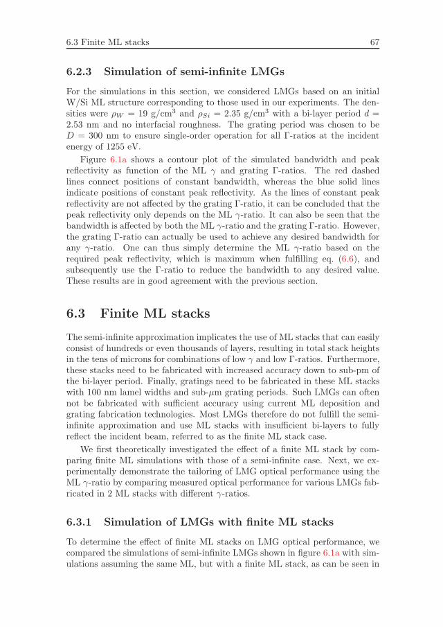
6.3 Finite ML stacks 67
6.2.3 Simulation of semi-infinite LMGs
For the simulations in this section, we considered LMGs based on an initialW/Si ML structure corresponding to those used in our experiments. The den-sities were ρW = 19 g/cm3 and ρSi = 2.35 g/cm3 with a bi-layer period d =2.53 nm and no interfacial roughness. The grating period was chosen to beD = 300 nm to ensure single-order operation for all Γ-ratios at the incidentenergy of 1255 eV.
Figure 6.1a shows a contour plot of the simulated bandwidth and peakreflectivity as function of the ML γ and grating Γ-ratios. The red dashedlines connect positions of constant bandwidth, whereas the blue solid linesindicate positions of constant peak reflectivity. As the lines of constant peakreflectivity are not affected by the grating Γ-ratio, it can be concluded that thepeak reflectivity only depends on the ML γ-ratio. It can also be seen that thebandwidth is affected by both the ML γ-ratio and the grating Γ-ratio. However,the grating Γ-ratio can actually be used to achieve any desired bandwidth forany γ-ratio. One can thus simply determine the ML γ-ratio based on therequired peak reflectivity, which is maximum when fulfilling eq. (6.6), andsubsequently use the Γ-ratio to reduce the bandwidth to any desired value.These results are in good agreement with the previous section.
6.3 Finite ML stacks
The semi-infinite approximation implicates the use of ML stacks that can easilyconsist of hundreds or even thousands of layers, resulting in total stack heightsin the tens of microns for combinations of low γ and low Γ-ratios. Furthermore,these stacks need to be fabricated with increased accuracy down to sub-pm ofthe bi-layer period. Finally, gratings need to be fabricated in these ML stackswith 100 nm lamel widths and sub-μm grating periods. Such LMGs can oftennot be fabricated with sufficient accuracy using current ML deposition andgrating fabrication technologies. Most LMGs therefore do not fulfill the semi-infinite approximation and use ML stacks with insufficient bi-layers to fullyreflect the incident beam, referred to as the finite ML stack case.
We first theoretically investigated the effect of a finite ML stack by com-paring finite ML simulations with those of a semi-infinite case. Next, we ex-perimentally demonstrate the tailoring of LMG optical performance using theML γ-ratio by comparing measured optical performance for various LMGs fab-ricated in 2 ML stacks with different γ-ratios.
6.3.1 Simulation of LMGs with finite ML stacks
To determine the effect of finite ML stacks on LMG optical performance, wecompared the simulations of semi-infinite LMGs shown in figure 6.1a with sim-ulations assuming the same ML, but with a finite ML stack, as can be seen in
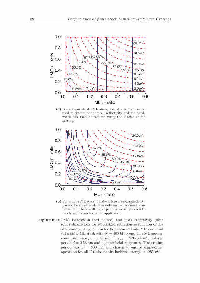
68 Performance of finite stack Lamellar Multilayer Gratings
(a) For a semi-infinite ML stack, the ML γ-ratio can beused to determine the peak reflectivity and the band-width can then be reduced using the Γ-ratio of thegrating.
(b) For a finite ML stack, bandwidth and peak reflectivitycannot be considered separately and an optimal com-bination of bandwidth and peak reflectivity needs tobe chosen for each specific application.
Figure 6.1: LMG bandwidth (red dotted) and peak reflectivity (bluesolid) simulations for s-polarized radiation as function of theML γ and grating Γ-ratio for (a) a semi-infinite ML stack and(b) a finite ML stack with N = 400 bi-layers. The ML param-eters used were ρW = 19 g/cm3, ρSi = 2.35 g/cm3, bi-layerperiod d = 2.53 nm and no interfacial roughness. The gratingperiod was D = 300 nm and chosen to ensure single-orderoperation for all Γ-ratios at the incident energy of 1255 eV.
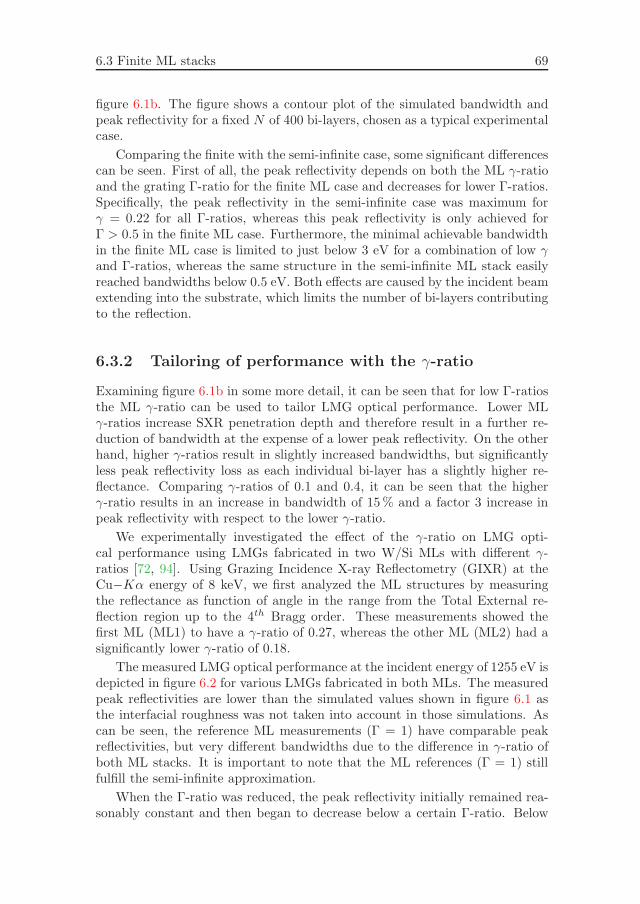
6.3 Finite ML stacks 69
figure 6.1b. The figure shows a contour plot of the simulated bandwidth andpeak reflectivity for a fixed N of 400 bi-layers, chosen as a typical experimentalcase.
Comparing the finite with the semi-infinite case, some significant differencescan be seen. First of all, the peak reflectivity depends on both the ML γ-ratioand the grating Γ-ratio for the finite ML case and decreases for lower Γ-ratios.Specifically, the peak reflectivity in the semi-infinite case was maximum forγ = 0.22 for all Γ-ratios, whereas this peak reflectivity is only achieved forΓ > 0.5 in the finite ML case. Furthermore, the minimal achievable bandwidthin the finite ML case is limited to just below 3 eV for a combination of low γand Γ-ratios, whereas the same structure in the semi-infinite ML stack easilyreached bandwidths below 0.5 eV. Both effects are caused by the incident beamextending into the substrate, which limits the number of bi-layers contributingto the reflection.
6.3.2 Tailoring of performance with the γ-ratio
Examining figure 6.1b in some more detail, it can be seen that for low Γ-ratiosthe ML γ-ratio can be used to tailor LMG optical performance. Lower MLγ-ratios increase SXR penetration depth and therefore result in a further re-duction of bandwidth at the expense of a lower peak reflectivity. On the otherhand, higher γ-ratios result in slightly increased bandwidths, but significantlyless peak reflectivity loss as each individual bi-layer has a slightly higher re-flectance. Comparing γ-ratios of 0.1 and 0.4, it can be seen that the higherγ-ratio results in an increase in bandwidth of 15% and a factor 3 increase inpeak reflectivity with respect to the lower γ-ratio.
We experimentally investigated the effect of the γ-ratio on LMG opti-cal performance using LMGs fabricated in two W/Si MLs with different γ-ratios [72, 94]. Using Grazing Incidence X-ray Reflectometry (GIXR) at theCu−Kα energy of 8 keV, we first analyzed the ML structures by measuringthe reflectance as function of angle in the range from the Total External re-flection region up to the 4th Bragg order. These measurements showed thefirst ML (ML1) to have a γ-ratio of 0.27, whereas the other ML (ML2) had asignificantly lower γ-ratio of 0.18.
The measured LMG optical performance at the incident energy of 1255 eV isdepicted in figure 6.2 for various LMGs fabricated in both MLs. The measuredpeak reflectivities are lower than the simulated values shown in figure 6.1 asthe interfacial roughness was not taken into account in those simulations. Ascan be seen, the reference ML measurements (Γ = 1) have comparable peakreflectivities, but very different bandwidths due to the difference in γ-ratio ofboth ML stacks. It is important to note that the ML references (Γ = 1) stillfulfill the semi-infinite approximation.
When the Γ-ratio was reduced, the peak reflectivity initially remained rea-sonably constant and then began to decrease below a certain Γ-ratio. Below
70 Performance of finite stack Lamellar Multilayer Gratings
that Γ-ratio the incident beam began to extend into the substrate and, hence,this indicated the transition from the semi-infinite to the finite ML case. TheΓ-ratio at which this occurred was roughly 0.4 for ML1 and 0.6 for ML2. Thebandwidth of both MLs also reduced towards lower Γ-ratios. In the semi-infiniteregion the bandwidth scaled linearly with Γ. Once the finite ML region wasreached, the bandwidth began to asymptotically approach a minimal value asthe minimal achievable bandwidth was then limited by the number of bi-layersin the ML.
(a) (b)
Figure 6.2: Comparison of (a) bandwidth and (b) peak reflectivity for twoMLs with different γ-ratios.
However, the peak reflectivity of LMGs with low Γ-ratios differs for bothMLs. ML2 had a lower γ-ratio, which resulted in narrower bandwidths andlower peak reflectivities. On the other hand, ML1 had a larger γ-ratio andtherefore resulted in a slightly higher bandwidth by a few tenths of eV. However,the peak reflectivity was increased by almost a factor 2. In fact, the peakreflectivity of ML1 should actually have been even higher, but was limited dueto a linear increase (chirp) of the bi-layer period in the depth of the ML asexplained in more detail in ref. [7]. ML2 had a significantly lower chirp, whichdid not affect the optical performance of the LMGs fabricated in that ML. LMGoptical performance can thus be tailored to maximize bandwidth reduction orminimize peak reflectivity loss using the ML γ-ratio.
6.4 Conclusions
We have analyzed the dependence of Lamellar Multilayer Grating (LMG) opti-cal performance, in terms of bandwidth and peak reflectivity, on various prac-tical limitations. Specifically, we have investigated how the number of bi-layersin the multilayer (ML) stack affects LMG performance. We first studied theidealized case of a semi-infinite ML stack, which is an often used approximationfor ML and LMG design. For the semi-infinite case, LMGs can be designed by
6.4 Conclusions 71
first optimizing the absorber-thickness-to-bi-layer period ratio γ of the ML toachieve maximum peak reflectivity. The bandwidth can then be subsequentlyreduced to any desired value using the lamel-width-to-grating-period ratio Γ.The lamel width of the grating is then determined from the single-order con-dition and the grating period is selected based on the required Γ-ratio.
However, the semi-infinite ML approximation generally requires ML stacksof hundreds to thousands of bi-layers, resulting in total stack heights of severalmicrons. These stacks also need to be deposited with sub-pm accuracy. Grat-ings then need to be fabricated in these ML stacks with lamel widths in theorder of 100 nm and sub-μm grating periods. Such structures can generallynot be deposited or etched with adequate precision using current technologies.LMGs are therefore often fabricated in ML stacks with insufficient bi-layersto fulfill the semi-infinite approximation, referred to as the finite ML case. Acriteria for the transition from the semi-infinite to finite ML case was derivedbased on the SXR penetration depth.
To determine the effect of a finite ML stack, simulations of LMG opticalperformance comparing the semi-infinite and finite ML case were performed.For the finite ML stack, the minimal achievable bandwidth and maximum peakreflectivity are limited by the number of bi-layers in the ML stack. Opticalperformance can then be further tailored using the ML γ-ratio. A lower γ-ratiowill result in slightly narrower bandwidths at the expense of peak reflectivity.If slightly higher bandwidths can be accepted, higher γ-ratios should be usedto minimize peak reflectivity loss. This was also experimentally demonstratedfor LMGs fabricated in two W/Si MLs with different γ-ratios of 0.18 and 0.27.For LMGs with low Γ-ratios, the higher ML γ resulted in a few tenths of eVlarger bandwidth, but almost doubled the peak reflectivity as compared to thelower ML γ.

7Lifetime of patterned
W/Si multilayer mirrors
7.1 Introduction
The fabrication of diffractive elements in multilayer (ML) mirrors can provideBragg-Fresnel optics for the EUV and soft x-ray (SXR) spectral ranges withunique properties. An important example are Lamellar Multilayer Gratings(LMGs) which provide improved spectral resolution with minimal loss of peakreflectivity [5–7] for soft x-ray (SXR) spectroscopy applications.
The practical usability of such optics depends on their lifetime, which canbe reduced by several degradation processes [95–99]. In particular, we distin-guish degradation due to surface phenomena and internal changes to the MLstructure. Surface phenomena include sidewall contamination due to the fab-rication process or the cracking of hydrocarbons, for instance from photoresistor cables in the vacuum system holding the ML mirror [96, 97, 100, 101]. Thecontamination results in additional absorption and hence reduces peak reflec-tivity of LMGs. Internal ML structure changes can be caused by intermixingdue to thermal annealing or diffusion of elements such as oxygen into the MLstructure. This can result in a change in the bi-layer period or reduce the opti-cal contrast between the absorber and spacer layer in the ML stack [102–106].As a consequence of these structural ML changes, the optical performance ofLMGs in terms of bandwidth, peak reflectivity and/or peak position, can beaffected.
Compared to conventional ML mirrors, the fabrication of optical elementssuch as LMGs increases their vulnerability to degradation processes. The fab-rication process described in chapter 4 [74] includes several steps in which the
74 Lifetime of patterned W/Si multilayer mirrors
ML structure is exposed to conditions that may enhance degradation of the MLstructure. These include steps in which increased temperatures are used, andwhere fluorine and oxygen radicals can chemically react with the ML materials.Furthermore, carbon-fluorine components are deposited on the sidewalls of theLMG structure in the course of the fabrication process to achieve a directionaletch. The fabrication of LMGs also increases the surface area between theML and vacuum by easily an order of magnitude as compared to conventionalML mirrors and directly exposes the ML structure to the various degradationprocesses.
In this chapter, we present a fabrication and storage lifetime study of Lamel-lar Multilayer Gratings (LMGs) fabricated in W/Si ML mirrors. In section 7.2we first investigate various potential degradation processes, including sidewallcontamination, thermal annealing and oxygen diffusion. SXR reflectivity wasdetermined to remain stable to within measurement accuracy over an extendedperiod of time as discussed in section 7.2. Radiation induced processes, such asthe cracking of hydrocarbons and intermixing of the ML stack [95–97, 100, 101],were not investigated in this work. A preliminary study into the use of cap-ping layers to protect the patterned MLs from degradation and carbon removalmethods is presented in section 7.3.
Although in this study we focused on the lifetime and degradation of LMGs,various other types of Bragg-Fresnel optics can be made using the same fabrica-tion process and be stored under the same conditions. This study can thereforealso be used to predict degradation of the broader class of Bragg-Fresnel opticsbased on patterned W/Si ML mirrors.
7.2 Potential degradation processes
In this section, we examine the effect of various potential degradation processes.We first examined sidewall contamination, which is a process limited to thesurface of the LMG. Next, processes affecting the ML internal structure, suchas thermal annealing and oxygen diffusion, were investigated. Finally, thestability of SXR reflectivity was investigated over a storage period extendingup to 18 months.
7.2.1 Sidewall contamination
To determine the effect of a sidewall contamination layer, we first measured itscomposition using x-ray photoelectron spectroscopy (XPS) and then theoreti-cally investigated the optical effect of using an extension to our Coupled WavesApproach (CWA) [5, 6].
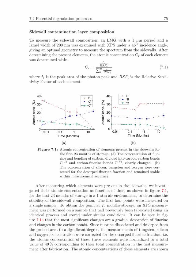
7.2 Potential degradation processes 75
Sidewall contamination layer composition
To measure the sidewall composition, an LMG with a 1 μm period and alamel width of 200 nm was examined with XPS under a 45 ◦ incidence angle,giving an optimal geometry to measure the spectrum from the sidewalls. Afterdetermining the present elements, the atomic concentration Cx of each elementwas determined with:
Cx =Ix
RSFx∑ni
IiRSFi
(7.1)
where Ii is the peak area of the photon peak and RSFi is the Relative Sensi-tivity Factor of each element.
(a) (b)
Figure 7.1: Atomic concentration of elements present in the sidewalls forthe first 23 months of storage. (a) The concentration of fluo-rine and bonding of carbon, divided into carbon-carbon bondsC(C) and carbon-fluorine bonds C(F ), clearly changed. (b)The concentration of silicon, tungsten and oxygen were cor-rected for the desorped fluorine fraction and remained stablewithin measurement accuracy.
After measuring which elements were present in the sidewalls, we investi-gated their atomic concentration as function of time, as shown in figure 7.1,for the first 23 months of storage in a 1 atm air environment, to determine thestability of the sidewall composition. The first four points were measured ona single sample. To obtain the point at 23 months storage, an XPS measure-ment was performed on a sample that had previously been fabricated using anidentical process and stored under similar conditions. It can be seen in fig-ure 7.1a that the most significant changes are a gradual desorption of fluorineand changes in the carbon bonds. Since fluorine dissociated and desorped fromthe probed area to a significant degree, the measurements of tungsten, siliconand oxygen concentration were corrected for the desorped fluorine fraction, i.e.the atomic concentration of those three elements were normalized to a totalvalue of 49% corresponding to their total concentration in the first measure-ment after fabrication. The atomic concentrations of these elements are shown
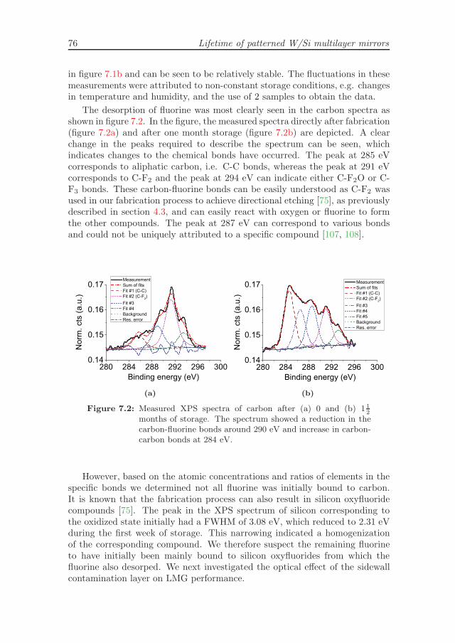
76 Lifetime of patterned W/Si multilayer mirrors
in figure 7.1b and can be seen to be relatively stable. The fluctuations in thesemeasurements were attributed to non-constant storage conditions, e.g. changesin temperature and humidity, and the use of 2 samples to obtain the data.
The desorption of fluorine was most clearly seen in the carbon spectra asshown in figure 7.2. In the figure, the measured spectra directly after fabrication(figure 7.2a) and after one month storage (figure 7.2b) are depicted. A clearchange in the peaks required to describe the spectrum can be seen, whichindicates changes to the chemical bonds have occurred. The peak at 285 eVcorresponds to aliphatic carbon, i.e. C-C bonds, whereas the peak at 291 eVcorresponds to C-F2 and the peak at 294 eV can indicate either C-F2O or C-F3 bonds. These carbon-fluorine bonds can be easily understood as C-F2 wasused in our fabrication process to achieve directional etching [75], as previouslydescribed in section 4.3, and can easily react with oxygen or fluorine to formthe other compounds. The peak at 287 eV can correspond to various bondsand could not be uniquely attributed to a specific compound [107, 108].
(a) (b)
Figure 7.2: Measured XPS spectra of carbon after (a) 0 and (b) 1 12
months of storage. The spectrum showed a reduction in thecarbon-fluorine bonds around 290 eV and increase in carbon-carbon bonds at 284 eV.
However, based on the atomic concentrations and ratios of elements in thespecific bonds we determined not all fluorine was initially bound to carbon.It is known that the fabrication process can also result in silicon oxyfluoridecompounds [75]. The peak in the XPS spectrum of silicon corresponding tothe oxidized state initially had a FWHM of 3.08 eV, which reduced to 2.31 eVduring the first week of storage. This narrowing indicated a homogenizationof the corresponding compound. We therefore suspect the remaining fluorineto have initially been mainly bound to silicon oxyfluorides from which thefluorine also desorped. We next investigated the optical effect of the sidewallcontamination layer on LMG performance.
7.2 Potential degradation processes 77
Effect of sidewall cover layers on LMG optical performance
To theoretically investigate the effect of a contamination layer on LMG opticalperformance, an extension to our Coupled Waves Approach (CWA) [5, 6] wasrequired (see also section 3.2.2). The theory for contamination layers can alsobe used for deliberately grown capping layers used to protect LMG structures.Here, we therefore refer to all layers as being cover layers when deriving thetheory.
To include the effect of cover layers in our CWA, the spatial distribution ofthe dielectric constant was rewritten to:
ε(x, z < 0) = 1; ε(x, z > H) = 1− χsub
ε(x, 0 ≤ z ≤ H) = 1− χ(z)U(x, z)− χpassV (x, z)(7.2)
where χ(z) is the susceptibility of a multilayer structure varying with the depth,while χcov and χsub are the constant susceptibility of the cover layer and sub-strate, respectively. The function U(x, z) = 1 if the point (x, z) is placed insidemultilayer structure and U = 0 otherwise. Similarly, the function V (x, z) = 1if the point (x, z) is placed inside the cover layer and otherwise equals 0.
Assuming the dielectric constant to be periodic function of x, we representedthe functions U and V as the Fourier series:
U(x, z) =
+∞∑n=−∞
Un(z)e2iπnx/D
V (x, z) =
+∞∑n=−∞
Vn(z)e2iπnx/D
(7.3)
where
Un(z) =sin(πnΓ)
πn
Vn(z) =2
πnsin
(πnh
D
)cos
[πn
(Γ
D+
h
D
)] (7.4)
with U0 = Γ and V0 = 2h/D. Please note that the terms U in eq. (4.3) differto those used in our previous works [5, 6] as the point x = 0 was now chosen tobe in the center of the lamel instead of at the left side of the lamel. Shifting thecoordinates of the previous works by x′ = x−ΓD/2 yields the same coefficientsas found here.
Following the same steps as in section 3.2 [5, 6], the 2D-wave equation∇2E(x, z) + k2ε(x, z)E(x, z) was solved, where ε is a periodic function of xand z described by eq. (7.2) and k is the wave vector given by 2π/λ. Thegeneral solution for the field F of the incident and reflected waves then has thefollowing form (chapter 1 in ref [66]):
F′′n (z) + κ2
nFn(Z) = k2∑m
[χ(z)Un−m(z) + χpassVn−m(z)]Fm(z) (7.5)
78 Lifetime of patterned W/Si multilayer mirrors
for n = 0,±1,±2, ... with boundary conditions:
F ′n(0) + iκnFn(0) = 2iκnδn,0;F
′n(L)− iκ(s)
n Fn(L) = 0. (7.6)
Here, κn =√k2 − q2n and κ
(s)n =
√k2εsub − q2n are the z-components of the
wave vectors for the nth diffraction order in vacuum and substrate, respectively,where qn = q0 + 2πn/D with q0 = k cosΘ0, and δn,0 is the Kronecker symbol.
To understand the effect of cover layers, we first recall the optical perfor-mance of a single-order LMG without a cover layer (h = 0) [5, 6]. In thiscase, the effective susceptibility χeff (z) = Γχ(z) corresponds to a conventionalML mirror with material densities reduced by a factor of Γ. The maximumachievable peak reflectivity, assuming abrupt interfaces, is then given by [4, 6]:
R0,peak =1− w
1 + w;
w =
√1− y2
1 + f2y2; f =
Re(χA − χS)
Im(χA − χS); y =
Im(χA − χS)
Im(χ)
sin(πjγ)
(πj)
(7.7)
Scaling the density of both materials by the same factor Γ does not changethe values of the parameters f and y and, hence, the peak reflectivity of asingle-order LMG is the same as that of a conventional ML mirror. At thesame time, the penetration depth LMS of the SXR wave into the LMG, whichdetermines the angular or spectral bandwidth, is given by:
LMS = Neff · d ∼ λ sinΘ0
πΓIm(χ)√(1 − y2)(1 + f2y2)
(7.8)
and is increased by a factor of 1/Γ. As Neff is then also increased by 1/Γ, thenumber of bi-layers in the LMG must therefore also be increased by the samefactor. The bandwidth is only scaled with the factor 1/Γ as the parameters fand y remain unchanged. Single-order LMGs therefore allow us to obtain anydesired resolution while maintaining high peak reflectivity under the assump-tion that the ML mirror contains sufficient bi-layers [5].
We then analyzed the effect of a cover layer with thickness h. The effectivesusceptibility of both materials in the ML structure is then increased by therelative amount of cover layer thickness with respect to the lamel, i.e. χeff (z) =Γχ(z)+2h/D ·χcov. The parameter f in eq. (7.7) only depends on the differencebetween the absorber and spacer layer susceptibility and is hence unaffectedby the cover layer. However, y depends on the average absorption, i.e. theimaginary part of the effective susceptibility, and was rewritten to:
y =Im(χA − χS)
Im(χS + 2h/(ΓD) · χcov)· sin(πjγ)
(πj)(7.9)
The parameter y is thus reduced due to the cover layer and from eqs. (7.7)and (7.8) it can be seen that this results in a decrease of peak reflectivity andincrease in bandwidth [4].
7.2 Potential degradation processes 79
The cover layer should generally be as thin as possible to ensure minimaleffect on LMG optical performance. From eq. (7.9), we derived that the effectof a cover layer on the peak reflectivity is negligible if the layer thickness is:
h <<ΓD
2· Im(χS)
Im(χcov)(7.10)
A similar condition showing acceptable layer thicknesses to ensure negligibleeffects on the bandwidth was also derived:
h <<ΓD
2· γ · Im(χA)
Im(χcov)(7.11)
To ensure the effect of a cover layer on LMG optical performance is neg-ligible, both conditions should be fulfilled. By examining conditions (7.10)and (7.11), we concluded that the latter is automatically achieved when theformer is fulfilled. This is because a highly absorbing material is typically usedas absorber, meaning Im(χA) >> Im(χcov). The lowest absorbing material istypically used as spacer, meaning Im(χS) < Im(χcov).
To illustrate the effect of a cover layer on the optical performance of anLMG, we performed simulations of LMGs based on W/Si MLs with parameterscorresponding to those used in this work. The densities were taken to beρW = 19 g/cm3 and ρSi = 2.35 g/cm3, N = 400 bi-layers with period d =2.53 nm, absorber-thickness-to-bi-layer-period ratio γ = 0.28 and no interfacialroughness. The parameters of the grating were chosen to ensure single-orderoperation for the entire wavelength range of interest and were a grating periodD = 300 nm with a lamel-width-to-grating-period ratio Γ = 0.25.
Figure 7.3 demonstrates the effect of a silicon oxyfluoride cover layer, whichwere the three main measured elements present in the sidewall, on LMG per-formance. As can be seen in figure 7.3a, the effect on the 0th and ±1st ordersis indeed very small for the measured cover layer thickness of 5 nm. The peakreflectivity drops by only 1 pp (3 relative % drop) and the bandwidth is in-creased by less than 1 relative %. According to eq. (7.10), the LMG opticalperformance should be significantly affected by a cover layer with a thickness of20 nm or more. A simulation of such a layer is shown in figure 7.3 and clearlyshows that such a layer indeed starts to reduce the peak reflectivity (5 pp,11 relative %) and increase the bandwidth (> 3 relative %) significantly. Asexpected from conditions (7.10) and (7.11) the cover layer indeed has a muchstronger effect on peak reflectivity than on bandwidth. Finally, both oxygen(540 eV) and fluorine (690 eV) have absorption edges within the simulatedregion. As can be seen in figure 7.3b peak reflectivity is reduced even furtherand the bandwidth is slightly increased just above these edges.
Using both scanning and transmission electron microscopy, we determinedour contamination layer to be well below 20 nm. Assuming a 5 nm contami-nation layer with a composition as determined from the XPS measurements,we determined the optical effect of the contamination layer to result in at
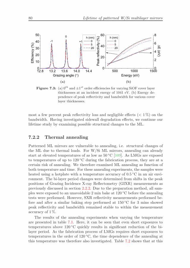
80 Lifetime of patterned W/Si multilayer mirrors
(a) (b)
Figure 7.3: (a) 0th and ±1st order efficiencies for varying SiOF cover layerthicknesses at an incident energy of 1041 eV. (b) Energy de-pendence of peak reflectivity and bandwidth for various coverlayer thicknesses.
most a few percent peak reflectivity loss and negligible effects (< 1%) on thebandwidth. Having investigated sidewall degradation effects, we continue ourlifetime study by examining possible structural changes to the ML.
7.2.2 Thermal annealing
Patterned ML mirrors are vulnerable to annealing, i.e. structural changes ofthe ML due to thermal loads. For W/Si ML mirrors, annealing can alreadystart at elevated temperatures of as low as 50 ◦C [109]. As LMGs are exposedto temperatures of up to 120 ◦C during the fabrication process, they are at acertain risk of annealing. We therefore examined ML annealing as function ofboth temperature and time. For these annealing experiments, the samples wereheated using a hotplate with a temperature accuracy of 0.5 ◦C in an air envi-ronment. The bi-layer period changes were determined from shifts in the peakpositions of Grazing Incidence X-ray Reflectometry (GIXR) measurements aspreviously discussed in section 2.2.2. Due to the preparation method, all sam-ples were exposed to an unavoidable 2 min bake at 120 ◦C before the annealingtests were performed. However, SXR reflectivity measurements performed be-fore and after a similar baking step performed at 150 ◦C for 3 mins showedpeak reflectivity and bandwidth remained stable to within the measurementaccuracy of 1%.
The results of the annealing experiments when varying the temperatureare presented in table 7.1. Here, it can be seen that even short exposures totemperatures above 120 ◦C quickly results in significant reduction of the bi-layer period. As the fabrication process of LMGs requires short exposures totemperatures in the order of 120 ◦C, the time dependence of the annealing atthis temperature was therefore also investigated. Table 7.2 shows that at this
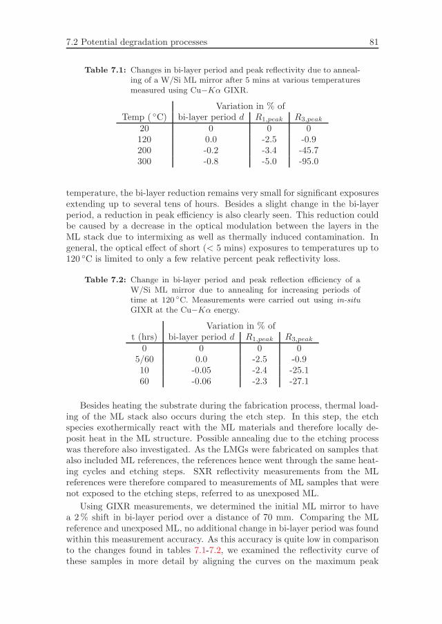
7.2 Potential degradation processes 81
Table 7.1: Changes in bi-layer period and peak reflectivity due to anneal-ing of a W/Si ML mirror after 5 mins at various temperaturesmeasured using Cu−Kα GIXR.
Variation in % ofTemp ( ◦C) bi-layer period d R1,peak R3,peak
20 0 0 0120 0.0 -2.5 -0.9200 -0.2 -3.4 -45.7300 -0.8 -5.0 -95.0
temperature, the bi-layer reduction remains very small for significant exposuresextending up to several tens of hours. Besides a slight change in the bi-layerperiod, a reduction in peak efficiency is also clearly seen. This reduction couldbe caused by a decrease in the optical modulation between the layers in theML stack due to intermixing as well as thermally induced contamination. Ingeneral, the optical effect of short (< 5 mins) exposures to temperatures up to120 ◦C is limited to only a few relative percent peak reflectivity loss.
Table 7.2: Change in bi-layer period and peak reflection efficiency of aW/Si ML mirror due to annealing for increasing periods oftime at 120 ◦C. Measurements were carried out using in-situGIXR at the Cu−Kα energy.
Variation in % oft (hrs) bi-layer period d R1,peak R3,peak
0 0 0 05/60 0.0 -2.5 -0.910 -0.05 -2.4 -25.160 -0.06 -2.3 -27.1
Besides heating the substrate during the fabrication process, thermal load-ing of the ML stack also occurs during the etch step. In this step, the etchspecies exothermically react with the ML materials and therefore locally de-posit heat in the ML structure. Possible annealing due to the etching processwas therefore also investigated. As the LMGs were fabricated on samples thatalso included ML references, the references hence went through the same heat-ing cycles and etching steps. SXR reflectivity measurements from the MLreferences were therefore compared to measurements of ML samples that werenot exposed to the etching steps, referred to as unexposed ML.
Using GIXR measurements, we determined the initial ML mirror to havea 2% shift in bi-layer period over a distance of 70 mm. Comparing the MLreference and unexposed ML, no additional change in bi-layer period was foundwithin this measurement accuracy. As this accuracy is quite low in comparisonto the changes found in tables 7.1-7.2, we examined the reflectivity curve ofthese samples in more detail by aligning the curves on the maximum peak
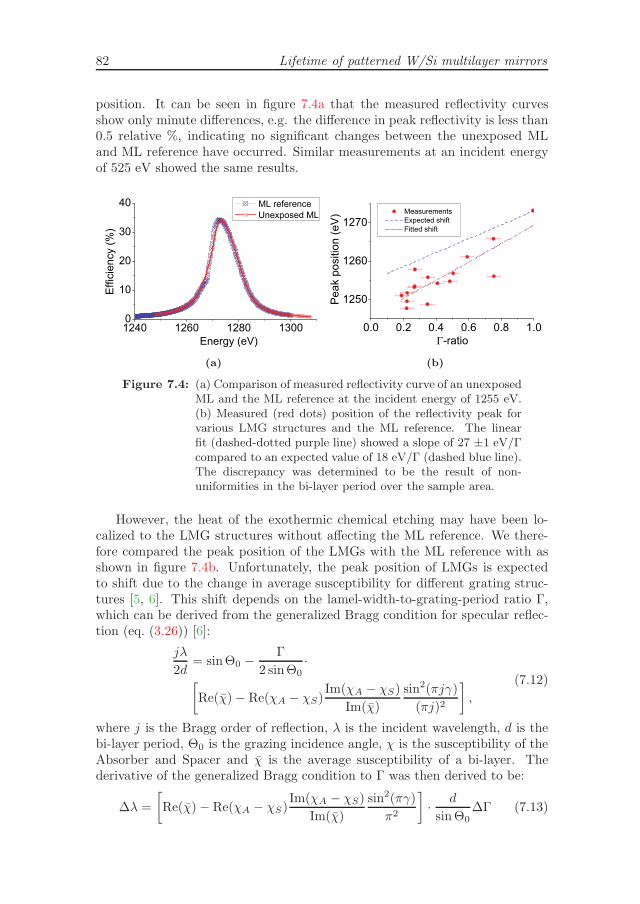
82 Lifetime of patterned W/Si multilayer mirrors
position. It can be seen in figure 7.4a that the measured reflectivity curvesshow only minute differences, e.g. the difference in peak reflectivity is less than0.5 relative %, indicating no significant changes between the unexposed MLand ML reference have occurred. Similar measurements at an incident energyof 525 eV showed the same results.
(a) (b)
Figure 7.4: (a) Comparison of measured reflectivity curve of an unexposedML and the ML reference at the incident energy of 1255 eV.(b) Measured (red dots) position of the reflectivity peak forvarious LMG structures and the ML reference. The linearfit (dashed-dotted purple line) showed a slope of 27 ±1 eV/Γcompared to an expected value of 18 eV/Γ (dashed blue line).The discrepancy was determined to be the result of non-uniformities in the bi-layer period over the sample area.
However, the heat of the exothermic chemical etching may have been lo-calized to the LMG structures without affecting the ML reference. We there-fore compared the peak position of the LMGs with the ML reference with asshown in figure 7.4b. Unfortunately, the peak position of LMGs is expectedto shift due to the change in average susceptibility for different grating struc-tures [5, 6]. This shift depends on the lamel-width-to-grating-period ratio Γ,which can be derived from the generalized Bragg condition for specular reflec-tion (eq. (3.26)) [6]:
jλ
2d= sinΘ0 − Γ
2 sinΘ0·[
Re(χ)− Re(χA − χS)Im(χA − χS)
Im(χ)
sin2(πjγ)
(πj)2
],
(7.12)
where j is the Bragg order of reflection, λ is the incident wavelength, d is thebi-layer period, Θ0 is the grazing incidence angle, χ is the susceptibility of theAbsorber and Spacer and χ is the average susceptibility of a bi-layer. Thederivative of the generalized Bragg condition to Γ was then derived to be:
Δλ =
[Re(χ)− Re(χA − χS)
Im(χA − χS)
Im(χ)
sin2(πγ)
π2
]· d
sinΘ0ΔΓ (7.13)
7.2 Potential degradation processes 83
To calculate the expected peak shift for LMGs, we used the same ML param-eters as in section 7.2.1. At the incident energy of 1255 eV, this results inΔλ ≈ 0.015ΔΓ or, equivalently, an slope in energy versus Γ of ≈ 18ΔΓ. How-ever, a slope of 27±1 eV/Γ was found when fitting the measured peak positionas function of the Γ-ratio. The same relative discrepancy was also found forthe measurements at an incident energy of 525 eV. We determined the differ-ence between the fitted and expected shift of figure 7.4b to correlate with theposition of the LMG on the sample area.
As changes to the bi-layer period could again not be measured with sufficientaccuracy to determine ML structural changes, we investigated the dependenceof LMG optical performance on the grating parameters. Although this compar-ison showed minor differences of a few relative percent in peak reflectivity, thisdifference scaled with the number of sidewalls and was nicely explained by thesidewall contamination layer. Changes in optical performance due to the LMGfabrication process were therefore determined to be below the measurementaccuracy of 0.1 pp peak reflectivity and 0.1 eV bandwidth.
7.2.3 Oxygen diffusion
The sidewalls of patternedW/Si ML mirrors contained large amounts of oxygenas discussed in section 7.2.1, which is known to affect optical performance ofMo/Si multilayer optics used for EUV lithography [97, 100]. Although oxygendiffusion is not expected to occur to a significant degree in our W/Si MLs [85,110], the fabrication of LMGs does increase the risk of oxygen diffusion. Wetherefore measured SXR peak reflectivity around the oxygen edge for 3 LMGswith varying grating periods and comparable Γ-ratios. These measurementswere carried out after 23 months of storage in a 1 atm air environment, allowingample time for diffusion of oxygen into the ML. Figure 7.5 shows the results ofthese measurements, where the ML reference measurement in figure 7.5a wasshifted in peak reflectivity to compensate for peak reflectivity loss due to thegrating structure of the LMGs.
Examining figure 7.5a, it can clearly be seen that the dip at 531 eV isonly present in the LMG samples. The depth of this dip was plotted againstthe sidewall-to-lamel-width ratio (2h/(ΓD)), showing a clear dependence onthe grating structure and, hence, the number of sidewalls the soft x-rays passthrough. From the dip position, we determined this dip was caused by tungstenoxides [107, 111]. Using the simulations of the previous section, we determineda 3 nm tungsten oxide layer on the sidewalls is required to explain the depth ofthe dip. This layer thickness was compared to the layer thickness determinedfrom the XPS measurements. In those measurements, we found an atomicconcentration of approximately 10% tungsten oxide. Assuming a sample depthfor the XPS of 5 nm, this results in a 0.5 nm tungsten oxide layer. However, thesimulations used purely theoretical cross-sections from ref. [23] and the XPSmeasurements assumed a homogenous sidewall layer as well as a 5 nm sampledepth, resulting in an estimation accuracy of the tungsten layer thickness of
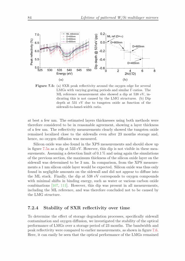
84 Lifetime of patterned W/Si multilayer mirrors
(a) (b)
Figure 7.5: (a) SXR peak reflectivity around the oxygen edge for severalLMGs with varying grating periods and similar Γ-ratios. TheML reference measurement also showed a dip at 538 eV, in-dicating this is not caused by the LMG structures. (b) Dipdepth at 531 eV due to tungsten oxide as function of thesidewall-to-lamel-width ratio.
at best a few nm. The estimated layers thicknesses using both methods weretherefore considered to be in reasonable agreement, showing a layer thicknessof a few nm. The reflectivity measurements clearly showed the tungsten oxideremained localized close to the sidewalls even after 23 months storage and,hence, no oxygen diffusion was measured.
Silicon oxide was also found in the XPS measurements and should show upin figure 7.5a as a dip at 533 eV. However, this dip is not visible in these mea-surements. Assuming a detection limit of 0.1% and using again the simulationsof the previous section, the maximum thickness of the silicon oxide layer on thesidewall was determined to be 3 nm. In comparison, from the XPS measure-ments a 1 nm silicon oxide layer would be expected. Silicon oxide was thus onlyfound in negligible amounts on the sidewall and did not appear to diffuse intothe ML stack. Finally, the dip at 538 eV corresponds to oxygen compoundswith minimal shifts in binding energy, such as water or various carbon oxidecombinations [107, 111]. However, this dip was present in all measurements,including the ML reference, and was therefore concluded not to be caused bythe LMG structure.
7.2.4 Stability of SXR reflectivity over time
To determine the effect of storage degradation processes, specifically sidewallcontamination and oxygen diffusion, we investigated the stability of the opticalperformance of LMGs over a storage period of 23 months. The bandwidth andpeak reflectivity were compared to earlier measurements, as shown in figure 7.6.Here, it can easily be seen that the optical performance of the LMGs remained
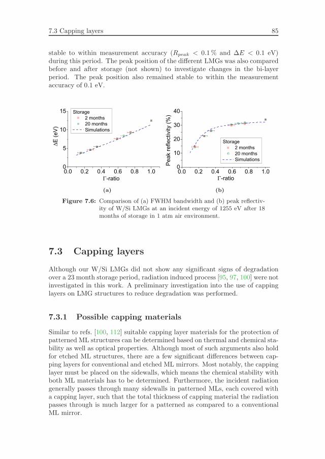
7.3 Capping layers 85
stable to within measurement accuracy (Rpeak < 0.1% and ΔE < 0.1 eV)during this period. The peak position of the different LMGs was also comparedbefore and after storage (not shown) to investigate changes in the bi-layerperiod. The peak position also remained stable to within the measurementaccuracy of 0.1 eV.
(a) (b)
Figure 7.6: Comparison of (a) FWHM bandwidth and (b) peak reflectiv-ity of W/Si LMGs at an incident energy of 1255 eV after 18months of storage in 1 atm air environment.
7.3 Capping layers
Although our W/Si LMGs did not show any significant signs of degradationover a 23 month storage period, radiation induced process [95, 97, 100] were notinvestigated in this work. A preliminary investigation into the use of cappinglayers on LMG structures to reduce degradation was performed.
7.3.1 Possible capping materials
Similar to refs. [100, 112] suitable capping layer materials for the protection ofpatterned ML structures can be determined based on thermal and chemical sta-bility as well as optical properties. Although most of such arguments also holdfor etched ML structures, there are a few significant differences between cap-ping layers for conventional and etched ML mirrors. Most notably, the cappinglayer must be placed on the sidewalls, which means the chemical stability withboth ML materials has to be determined. Furthermore, the incident radiationgenerally passes through many sidewalls in patterned MLs, each covered witha capping layer, such that the total thickness of capping material the radiationpasses through is much larger for a patterned as compared to a conventionalML mirror.
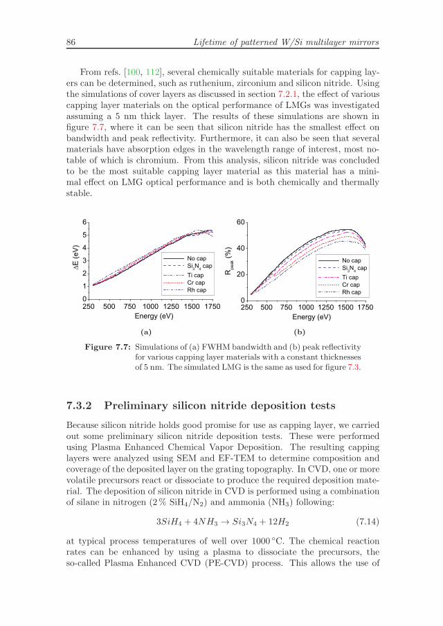
86 Lifetime of patterned W/Si multilayer mirrors
From refs. [100, 112], several chemically suitable materials for capping lay-ers can be determined, such as ruthenium, zirconium and silicon nitride. Usingthe simulations of cover layers as discussed in section 7.2.1, the effect of variouscapping layer materials on the optical performance of LMGs was investigatedassuming a 5 nm thick layer. The results of these simulations are shown infigure 7.7, where it can be seen that silicon nitride has the smallest effect onbandwidth and peak reflectivity. Furthermore, it can also be seen that severalmaterials have absorption edges in the wavelength range of interest, most no-table of which is chromium. From this analysis, silicon nitride was concludedto be the most suitable capping layer material as this material has a mini-mal effect on LMG optical performance and is both chemically and thermallystable.
(a) (b)
Figure 7.7: Simulations of (a) FWHM bandwidth and (b) peak reflectivityfor various capping layer materials with a constant thicknessesof 5 nm. The simulated LMG is the same as used for figure 7.3.
7.3.2 Preliminary silicon nitride deposition tests
Because silicon nitride holds good promise for use as capping layer, we carriedout some preliminary silicon nitride deposition tests. These were performedusing Plasma Enhanced Chemical Vapor Deposition. The resulting cappinglayers were analyzed using SEM and EF-TEM to determine composition andcoverage of the deposited layer on the grating topography. In CVD, one or morevolatile precursors react or dissociate to produce the required deposition mate-rial. The deposition of silicon nitride in CVD is performed using a combinationof silane in nitrogen (2% SiH4/N2) and ammonia (NH3) following:
3SiH4 + 4NH3 → Si3N4 + 12H2 (7.14)
at typical process temperatures of well over 1000 ◦C. The chemical reactionrates can be enhanced by using a plasma to dissociate the precursors, theso-called Plasma Enhanced CVD (PE-CVD) process. This allows the use of
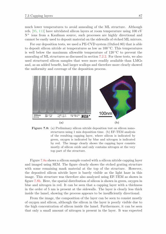
7.3 Capping layers 87
much lower temperatures to avoid annealing of the ML structure. Althoughrefs. [95, 113] have nitridated silicon layers at room temperature using 100 eVN+ ions from a Kaufman source, such processes are highly directional andcannot be easily used to deposit material on the sidewalls of etched ML mirrors.
For our deposition tests, we used a PE-CVD system (Oxford 80) that is ableto deposit silicon nitride at temperatures as low as 100 ◦C. This temperaturesis well below the maximum allowable temperature of 120 ◦C to prevent theannealing of ML structures as discussed in section 7.2.2. For these tests, we alsoused structured silicon samples that were more readily available than LMGsand, as an added benefit, had larger scallops and therefore more clearly showedthe uniformity and coverage of the deposition process.
(a)
100nm
(b)
Figure 7.8: (a) Preliminary silicon nitride deposition test on silicon nano-structures using 1 min deposition time. (b) EF-TEM analysisof the resulting capping layer, where silicon is indicated bygreen, oxygen is indicated by blue and nitrogen is indicatedby red. The image clearly shows the capping layer consistsmostly of silicon oxide and only contains nitrogen at the verytop part of the structure.
Figure 7.8a shows a silicon sample coated with a silicon nitride capping layerand imaged using SEM. The figure clearly shows the etched grating structurewith some remaining mask material at the top of the structure. However,the deposited silicon nitride layer is barely visible as the light haze in thisimage. This structure was therefore also analyzed using EF-TEM as shown infigure 7.8b. Here, the spatial distribution of silicon is shown in green, oxygen inblue and nitrogen in red. It can be seen that a capping layer with a thicknessin the order of 5 nm is present at the sidewalls. The layer is clearly less thickinside the lamel, showing the process appears to be insufficiently directional.
From the image, the composition of the layer can be seen to consist mostlyof oxygen and silicon, although the silicon in the layer is poorly visible due tothe high concentration of silicon inside the lamel. Furthermore, it can be seenthat only a small amount of nitrogen is present in the layer. It was expected
88 Lifetime of patterned W/Si multilayer mirrors
that although the plasma dissociated the silane and ammonia, the temperaturewas insufficient to nitridate the deposited silicon. This resulted in a depositionof a pure silicon layer which, when exposed to air, immediately oxidized andresulted in a layer of silicon oxide instead of the desired silicon nitride.
7.4 Conclusions
The lifetime of patterned multilayer (ML) mirrors is very important for theusability of these elements in practical applications. We therefore investigatedvarious degradation processes that could reduce this lifetime and that couldoccur during fabrication and storage during 23 months in 1 atm air environ-ment. This study was performed for Lamellar Multilayer Gratings (LMGs),which are optical elements used for soft x-ray spectroscopy, fabricated in W/SiML mirrors. The results are expected to also be applicable to other opticalelements fabricated in W/Si ML mirrors that were fabricated using the samefabrication process and stored under similar conditions.
We first investigated sidewall contamination as a surface phenomenon thatincreases the absorption and hence reduces peak reflectivity of LMGs. Thecomposition of the sidewall contamination layer was measured with x-ray pho-toelectron spectroscopy, showing a significant desorption of fluorine during stor-age. An extension to our Coupled Waves Approach (CWA) simulation methodwas derived to simulate the optical effect of this contamination layer. Crite-ria for acceptable contamination layer thicknesses for which peak reflectivityand bandwidth are not significantly affected were also derived. This analysisrevealed layers less than 5 nm with the measured composition had a limitedeffect of at most a few relative percent peak reflectivity loss.
Degradation due to structural changes to the ML caused by thermal an-nealing and oxygen diffusion were investigated next. This analysis showed theML was stable for long period (> 60 hrs) at 120 ◦C, but quickly deteriorated athigher temperatures. Oxygen diffusion was investigated using SXR reflectivitymeasurements around the oxygen edge, showing oxides were still localized tothe sidewall even after 23 months storage. To determine the overall effect ofstorage, we measured the stability of SXR reflectivity over an extended storageperiod of 18 months. This analysis showed the optical performance of LMGsto remain stable to within measurement accuracy during this period.
Though not studied here, degradation is expected to be enhanced underirradiation with soft x-ray photons. We therefore investigated various possi-ble capping layer materials to protect the LMG from degradation and duringcarbon cleaning processes. Suitable capping layers were theoretically studied,showing silicon nitride to be the preferred candidate. Preliminary depositiontests of silicon nitride were performed using plasma enhanced chemical vapordeposition at the low temperatures required to prevent annealing of the ML.However, these tests showed the resulting layer was poorly nitridated and didnot sufficiently cover the LMG topography for use as a capping layer.
8Conclusions
The ability to identify and quantify chemical elements in products is very im-portant to ensure, for instance, that steel and concrete are of sufficient qualityto be used for construction or that there are no toxic contaminants in ourfood or drinks. A major improvement in chemical element identification wasobtained after the discovery of x-rays. Elements could now be uniquely andnon-destructively identified by analyzing the fluorescent x-ray spectrum emit-ted after a sample had been irradiated with high energy x-rays, which is thebasic principle of x-ray fluorescence spectroscopy. To analyze the fluorescencespectrum, an optical element is required that separates x-rays with differentenergies. In the soft x-ray spectral range, which is of importance for identifyinglighter elements, such elements are often multilayer (ML) mirrors that work onthe principle of Bragg reflection. Unfortunately, the spectral resolution of MLmirrors is inherently limited in this range by the absorption of the fluorescentx-rays that need to be analyzed. The spectral resolution of ML mirrors can beimproved by fabricating a grating into the ML stack, resulting in a so-calledLamellar Multilayer Grating (LMG). However, the usability of LMGs has beenlimited due to challenges in simulation, which limited the understanding ofthe LMG working principles, and fabrication, which limited the grating dimen-sions and ML stack height of LMGs. In this thesis, a simulation and fabricationmethod were investigated which overcame the aforementioned limitations andimproved the usability of LMGs in practical applications.
We first derived a Coupled Waves Analysis (CWA) to simulate LMG opticalperformance in terms of bandwidth and peak reflectivity. This CWA describesthe change in amplitude of the incident and exiting waves as function of positionin the ML stack. Compared to previously used simulation methods, this CWAsignificantly reduces computation time, can simulate various non-ideal lamelshapes and allows for improved understanding of LMG operating principles.
90 Conclusions
Based on this CWA, we identified an optimal LMG operating regime, referredto as single-order operation, in which the incident beam excites only a singlediffraction order and, hence, is not affected by diffraction losses. For LMGsoperating in single-order, the optical performance is largely determined by thelamel-width-to-grating-period ratio Γ. The resolution of an LMG was derivedto scale with 1/Γ in comparison to a conventional ML mirror. LMG peakreflectivity was determined to be as high as that of a conventional ML mirrorif the number of bi-layers N was also increased by 1/Γ.
The fabrication of single-order operating LMGs requires the patterning ofnanoscale structures in MLs made of up to hundreds of thin bi-layers with aperiod of a few nm. These bi-layers consist of, at least, two materials of whichone is generally a high-Z material. Although e-beam lithography can be usedto define LMG structures, this is a time-consuming and costly process. Patterntransfer using Reactive Ion Etching (RIE) is generally insufficient accurate orreproducible. We therefore investigated the patterning of ML mirrors usingUV-NanoImprint Lithography and Bosch Deep Reactive Ion Etching (DRIE).This process provides accurate and reproducible fabrication of LMGs with sub-micron periods over tens of square mm2 area in an economic manner. The MLstructure itself was used to achieve optimal pattern transfer. In particular,the high-Z layer in the ML stack was used to suppress scallop formation andallow for low tapers with minimal grating structure dependence. Althoughthis fabrication study was performed for the patterning of grating structuresin W/Si ML mirrors, the approach and results are generally applicable to MLmirrors consisting of materials that react volatile with fluorine. Such MLsinclude Mo/Si for EUV lithography and Mo/B4C for spectroscopy. However,the activation energy of the reactions with fluorine as well as possible compoundformation in the ML structure can significantly affect etching. The minimaldependence on grating dimensions and low tapers of the derived process arehighly beneficial for the fabrication of optical elements with varying featuredimensions, such as zoneplates.
Reflectivity of single-order LMGs for the SXR spectral range was measuredand was found to be in good agreement with our CWA. Single-order LMGs hadlimited diffraction losses, which was evident from the absence of any significantsecondary structures besides the main Bragg peak and a corresponding increaseof the peak reflectivity with respect to a multi-order LMG having the same Γ-ratio. A record value of spectral resolution improvement was achieved usingsingle-order operation, which is currently a factor of 3.8 with regard to theunpatterned ML mirror. Excitation of higher diffraction orders in single-orderoperation was easily measured by varying the detector angle and was also ingood agreement with our CWA. Our CWA can thus also be used to investigatethe use of higher diffraction orders from LMGs for various applications. Finally,we determined non-uniformities of the bi-layer period in the depth of the initialML are currently limiting LMG performance. Further improvements of LMGperformance can therefore be obtained by increasing the ML deposition process.
Current technologies for ML deposition and grating fabrication actually
Conclusions 91
often do not achieve sufficient accuracy to fulfill the semi-infinite ML approx-imation. However, this approximation is often used for ML and LMG design.Assuming the semi-infinite approximation, LMGs can be designed by first op-timizing the absorber-thickness-to-bi-layer period γ of the ML to achieve maxi-mum peak reflectivity and subsequently reducing the bandwidth to any desiredvalue using the lamel-width-to-grating-period ratio Γ. In particular for LMGswith low Γ-ratio’s, this approximation is often not valid. We therefore deriveda criterion for the transition from the semi-infinite to finite ML case basedon the SXR penetration depth. To determine the effect of a finite ML stack,simulations of LMG optical performance comparing a semi-infinite and finiteML stacks were performed. For the finite ML stack, the minimal achievablebandwidth and maximum peak reflectivity are limited by the number of bi-layers in the ML stack. Optical performance can then be further tailored usingthe ML γ-ratio. A lower γ-ratio will result in slightly narrower bandwidths atthe expense of peak reflectivity. If slightly higher bandwidths can be accepted,higher γ-ratios should be used to minimize peak reflectivity loss.
Finally, we investigated degradation processes of patterned ML optics asthis can reduce the lifetime of such elements, which is important for theirusability in practical applications. In this work, we focused on degradationduring fabrication and storage during 23 months in a 1 atm air environment.The surface phenomenon of sidewall contamination showed a clear desorptionof fluorine, but limited optical effect for contamination layers with a thicknessbelow 5 nm. Internal ML structural changes due to thermal annealing or oxygendiffusion were not seen within measurement accuracy. The SXR reflectivityalso remained stable over an extended storage period of 18 months withinmeasurement accuracy. Radiation induced degradation processes, includingsurface photochemistry, need to be investigated separately. An investigationof possible capping layer materials was performed showing silicon nitride tobe the preferred candidate. Preliminary deposition tests of silicon nitride wereperformed using PE-CVD, but the resulting layer was poorly nitridated and didnot sufficiently cover the LMG topography for use as a capping layer. Althoughthe degradation study was performed for the specific case of LMGs, the resultsare expected to also be applicable to other Bragg-Fresnel optics fabricated inW/Si ML mirrors using the same fabrication process and stored under similarconditions.

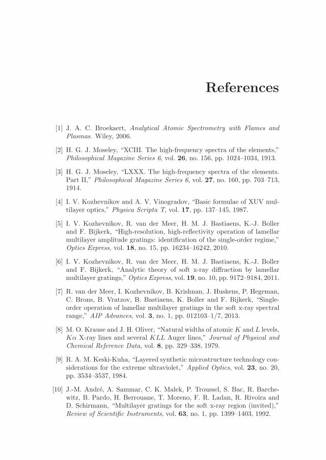
References
[1] J. A. C. Broekaert, Analytical Atomic Spectrometry with Flames andPlasmas. Wiley, 2006.
[2] H. G. J. Moseley, “XCIII. The high-frequency spectra of the elements,”Philosophical Magazine Series 6, vol. 26, no. 156, pp. 1024–1034, 1913.
[3] H. G. J. Moseley, “LXXX. The high-frequency spectra of the elements.Part II,” Philosophical Magazine Series 6, vol. 27, no. 160, pp. 703–713,1914.
[4] I. V. Kozhevnikov and A. V. Vinogradov, “Basic formulae of XUV mul-tilayer optics,” Physica Scripta T, vol. 17, pp. 137–145, 1987.
[5] I. V. Kozhevnikov, R. van der Meer, H. M. J. Bastiaens, K.-J. Bollerand F. Bijkerk, “High-resolution, high-reflectivity operation of lamellarmultilayer amplitude gratings: identification of the single-order regime,”Optics Express, vol. 18, no. 15, pp. 16234–16242, 2010.
[6] I. V. Kozhevnikov, R. van der Meer, H. M. J. Bastiaens, K.-J. Bollerand F. Bijkerk, “Analytic theory of soft x-ray diffraction by lamellarmultilayer gratings,” Optics Express, vol. 19, no. 10, pp. 9172–9184, 2011.
[7] R. van der Meer, I. Kozhevnikov, B. Krishnan, J. Huskens, P. Hegeman,C. Brons, B. Vratzov, B. Bastiaens, K. Boller and F. Bijkerk, “Single-order operation of lamellar multilayer gratings in the soft x-ray spectralrange,” AIP Advances, vol. 3, no. 1, pp. 012103–1/7, 2013.
[8] M. O. Krause and J. H. Oliver, “Natural widths of atomic K and L levels,Kα X-ray lines and several KLL Auger lines,” Journal of Physical andChemical Reference Data, vol. 8, pp. 329–338, 1979.
[9] R. A. M. Keski-Kuha, “Layered synthetic microstructure technology con-siderations for the extreme ultraviolet,” Applied Optics, vol. 23, no. 20,pp. 3534–3537, 1984.
[10] J.-M. Andre, A. Sammar, C. K. Malek, P. Troussel, S. Bac, R. Barche-witz, B. Pardo, H. Berrouane, T. Moreno, F. R. Ladan, R. Rivoira andD. Schirmann, “Multilayer gratings for the soft x-ray region (invited),”Review of Scientific Instruments, vol. 63, no. 1, pp. 1399–1403, 1992.
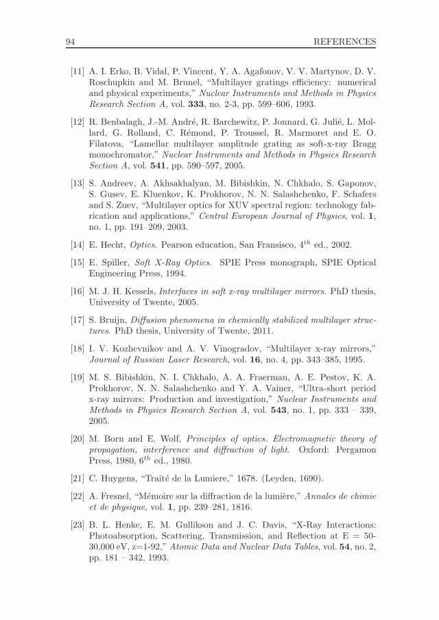
94 REFERENCES
[11] A. I. Erko, B. Vidal, P. Vincent, Y. A. Agafonov, V. V. Martynov, D. V.Roschupkin and M. Brunel, “Multilayer gratings efficiency: numericaland physical experiments,” Nuclear Instruments and Methods in PhysicsResearch Section A, vol. 333, no. 2-3, pp. 599–606, 1993.
[12] R. Benbalagh, J.-M. Andre, R. Barchewitz, P. Jonnard, G. Julie, L. Mol-lard, G. Rolland, C. Remond, P. Troussel, R. Marmoret and E. O.Filatova, “Lamellar multilayer amplitude grating as soft-x-ray Braggmonochromator,” Nuclear Instruments and Methods in Physics ResearchSection A, vol. 541, pp. 590–597, 2005.
[13] S. Andreev, A. Akhsakhalyan, M. Bibishkin, N. Chkhalo, S. Gaponov,S. Gusev, E. Kluenkov, K. Prokhorov, N. N. Salashchenko, F. Schafersand S. Zuev, “Multilayer optics for XUV spectral region: technology fab-rication and applications,” Central European Journal of Physics, vol. 1,no. 1, pp. 191–209, 2003.
[14] E. Hecht, Optics. Pearson education, San Fransisco, 4th ed., 2002.
[15] E. Spiller, Soft X-Ray Optics. SPIE Press monograph, SPIE OpticalEngineering Press, 1994.
[16] M. J. H. Kessels, Interfaces in soft x-ray multilayer mirrors. PhD thesis,University of Twente, 2005.
[17] S. Bruijn, Diffusion phenomena in chemically stabilized multilayer struc-tures. PhD thesis, University of Twente, 2011.
[18] I. V. Kozhevnikov and A. V. Vinogradov, “Multilayer x-ray mirrors,”Journal of Russian Laser Research, vol. 16, no. 4, pp. 343–385, 1995.
[19] M. S. Bibishkin, N. I. Chkhalo, A. A. Fraerman, A. E. Pestov, K. A.Prokhorov, N. N. Salashchenko and Y. A. Vainer, “Ultra-short periodx-ray mirrors: Production and investigation,” Nuclear Instruments andMethods in Physics Research Section A, vol. 543, no. 1, pp. 333 – 339,2005.
[20] M. Born and E. Wolf, Principles of optics. Electromagnetic theory ofpropagation, interference and diffraction of light. Oxford: PergamonPress, 1980, 6th ed., 1980.
[21] C. Huygens, “Traite de la Lumiere,” 1678. (Leyden, 1690).
[22] A. Fresnel, “Memoire sur la diffraction de la lumiere,” Annales de chimieet de physique, vol. 1, pp. 239–281, 1816.
[23] B. L. Henke, E. M. Gullikson and J. C. Davis, “X-Ray Interactions:Photoabsorption, Scattering, Transmission, and Reflection at E = 50-30,000 eV, z=1-92,” Atomic Data and Nuclear Data Tables, vol. 54, no. 2,pp. 181 – 342, 1993.
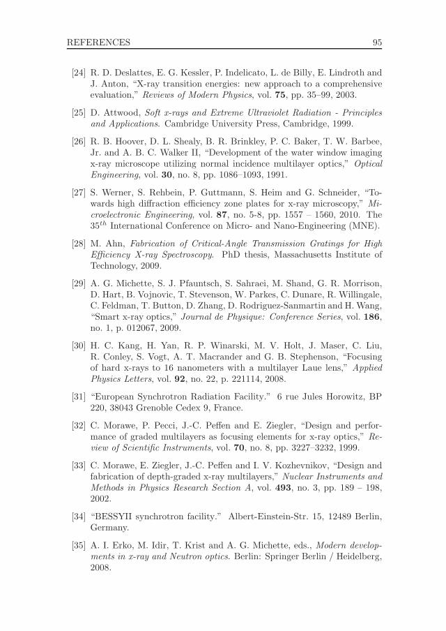
REFERENCES 95
[24] R. D. Deslattes, E. G. Kessler, P. Indelicato, L. de Billy, E. Lindroth andJ. Anton, “X-ray transition energies: new approach to a comprehensiveevaluation,” Reviews of Modern Physics, vol. 75, pp. 35–99, 2003.
[25] D. Attwood, Soft x-rays and Extreme Ultraviolet Radiation - Principlesand Applications. Cambridge University Press, Cambridge, 1999.
[26] R. B. Hoover, D. L. Shealy, B. R. Brinkley, P. C. Baker, T. W. Barbee,Jr. and A. B. C. Walker II, “Development of the water window imagingx-ray microscope utilizing normal incidence multilayer optics,” OpticalEngineering, vol. 30, no. 8, pp. 1086–1093, 1991.
[27] S. Werner, S. Rehbein, P. Guttmann, S. Heim and G. Schneider, “To-wards high diffraction efficiency zone plates for x-ray microscopy,” Mi-croelectronic Engineering, vol. 87, no. 5-8, pp. 1557 – 1560, 2010. The35th International Conference on Micro- and Nano-Engineering (MNE).
[28] M. Ahn, Fabrication of Critical-Angle Transmission Gratings for HighEfficiency X-ray Spectroscopy. PhD thesis, Massachusetts Institute ofTechnology, 2009.
[29] A. G. Michette, S. J. Pfauntsch, S. Sahraei, M. Shand, G. R. Morrison,D. Hart, B. Vojnovic, T. Stevenson, W. Parkes, C. Dunare, R. Willingale,C. Feldman, T. Button, D. Zhang, D. Rodriguez-Sanmartin and H. Wang,“Smart x-ray optics,” Journal de Physique: Conference Series, vol. 186,no. 1, p. 012067, 2009.
[30] H. C. Kang, H. Yan, R. P. Winarski, M. V. Holt, J. Maser, C. Liu,R. Conley, S. Vogt, A. T. Macrander and G. B. Stephenson, “Focusingof hard x-rays to 16 nanometers with a multilayer Laue lens,” AppliedPhysics Letters, vol. 92, no. 22, p. 221114, 2008.
[31] “European Synchrotron Radiation Facility.” 6 rue Jules Horowitz, BP220, 38043 Grenoble Cedex 9, France.
[32] C. Morawe, P. Pecci, J.-C. Peffen and E. Ziegler, “Design and perfor-mance of graded multilayers as focusing elements for x-ray optics,” Re-view of Scientific Instruments, vol. 70, no. 8, pp. 3227–3232, 1999.
[33] C. Morawe, E. Ziegler, J.-C. Peffen and I. V. Kozhevnikov, “Design andfabrication of depth-graded x-ray multilayers,” Nuclear Instruments andMethods in Physics Research Section A, vol. 493, no. 3, pp. 189 – 198,2002.
[34] “BESSYII synchrotron facility.” Albert-Einstein-Str. 15, 12489 Berlin,Germany.
[35] A. I. Erko, M. Idir, T. Krist and A. G. Michette, eds., Modern develop-ments in x-ray and Neutron optics. Berlin: Springer Berlin / Heidelberg,2008.
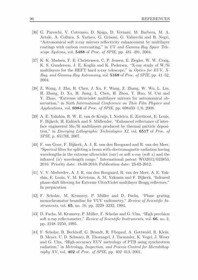
96 REFERENCES
[36] G. Pareschi, V. Cotroneo, D. Spiga, D. Vernani, M. Barbera, M. A.Artale, A. Collura, S. Varisco, G. Grisoni, G. Valsecchi and B. Negri,“Astronomical soft x-ray mirrors reflectivity enhancement by multilayercoatings with carbon overcoating,” in UV and Gamma-Ray Space Tele-scope Systems, vol. 5488 of Proc. of SPIE, pp. 481–491, 2004.
[37] K. K. Madsen, F. E. Christensen, C. P. Jensen, E. Ziegler, W. W. Craig,K. S. Gunderson, J. E. Koglin and K. Pedersen, “X-ray study of W/Simultilayers for the HEFT hard x-ray telescope,” in Optics for EUV, X-Ray, and Gamma-Ray Astronomy, vol. 5168 of Proc. of SPIE, pp. 41–52,2004.
[38] Z. Wang, J. Zhu, R. Chen, J. Xu, F. Wang, Z. Zhang, W. Wu, L. Liu,H. Zhang, D. Xu, H. Jiang, L. Chen, H. Zhou, T. Huo, M. Cui andY. Zhao, “Extreme ultraviolet multilayer mirrors for astronomical ob-servation,” in Sixth International Conference on Thin Film Physics andApplications, vol. 6984 of Proc. of SPIE, pp. 698433–1/6, 2008.
[39] A. E. Yakshin, R. W. E. van de Kruijs, I. Nedelcu, E. Zoethout, E. Louis,F. Bijkerk, H. Enkisch and S. Mullender, “Enhanced reflectance of inter-face engineered Mo/Si multilayers produced by thermal particle deposi-tion,” in Emerging Lithographic Technologies XI, vol. 6517 of Proc. ofSPIE, p. 65170I, 2007.
[40] F. van Goor, F. Bijkerk, A. J. R. van den Boogaard and R. van der Meer,“Spectral filter for splitting a beam with electromagnetic radiation havingwavelengths in the extreme ultraviolet (euv) or soft x-ray (soft x) and theinfrared (ir) wavelength range.” International patent WO2012/023853,2010. Priority date: 18-08-2010; Publication date: 23-02-2012.
[41] V. V. Medvedev, A. J. R. van den Boogaard, R. van der Meer, A. E. Yak-shin, E. Louis, V. M. Krivtsun, A. M. Yakunin and F. Bijkerk, “Infraredphase-shift filtering for Extreme UltraViolet multilayer Bragg reflectors.”In preparation.
[42] F. Scholze, M. Krumrey, P. Muller and D. Fuchs, “Plane gratingmonochromator beamline for VUV radiometry,” Review of Scientific In-struments, vol. 65, no. 10, pp. 3229–3232, 1994.
[43] D. Fuchs, M. Krumrey, P. Muller, F. Scholze and G. Ulm, “High precisionsoft x-ray reflectometer,” Review of Scientific Instruments, vol. 66, no. 2,pp. 2248–2250, 1995.
[44] F. Scholze, B. Beckhoff, G. Brandt, R. Fliegauf, A. Gottwald, R. Klein,B. Meyer, U. D. Schwarz, R. Thornagel, J. Tuemmler, K. Vogel, J. Weserand G. Ulm, “High-accuracy EUV metrology of PTB using synchrotronradiation,” in Metrology, Inspection, and Process Control for Microlithog-raphy XV, vol. 402 of Proc. of SPIE, pp. 402–413, 2001.
REFERENCES 97
[45] F. Scholze, J. Tummler and G. Ulm, “High-accuracy radiometry in theEUV range at the PTB soft x-ray beamline,” Metrologia, vol. 40, no. 1,p. S224, 2003.
[46] J. Daillant and A. Gibaud, X-ray and Neutron Reflectivity: Principlesand Applications. Lecture Notes in Physics, Springer, 2008.
[47] K. N. Stoev and K. Sakurai, “Review on grazing incidence x-ray spec-trometry and reflectometry,” Spectrochimica Acta Part B: Atomic Spec-troscopy, vol. 54, no. 1, pp. 41–82, 1999.
[48] D. L. Windt, “IMD–Software for modeling the optical properties of mul-tilayer films,” Computers in physics, vol. 12, pp. 360–370, 1998.
[49] P. E. Mix, Introduction to Nondestructive Testing: A Training Guide.John Wiley & Sons, 2005.
[50] L. Reimer and P. W. Hawkes, Scanning Electron Microscopy: Physics ofImage Formation and Microanalysis. Springer Series in Optical Sciences,Springer, 2010.
[51] L. Reimer and H. Kohl, Transmission Electron Microscopy: Physics ofImage Formation. Springer Series in Optical Sciences, Springer, 2008.
[52] P. van der Heide, X-ray Photoelectron Spectroscopy: An introduction toPrinciples and Practices. Wiley, 2011.
[53] J. F. Watts, “X-ray photoelectron spectroscopy,”Vacuum, vol. 45, no. 67,pp. 653 – 671, 1994. Special Issue Surface Science Techniques.
[54] B. Vidal, P. Vincent, M. Neviere and P. Dhez, “Thin films and gratings -Theories to optimize the high reflectivity of mirrors and gratings for x-rayoptics,” in Applications of Thin Film Multilayered Structures to FiguredX-Ray Optics, vol. 563 of Proc. of SPIE, pp. 142–149, 1985.
[55] S. T. Peng, “Rigorous formulation of scattering and guidance by dielectricgrating waveguides: general case of oblique incidence,” Journal of theOptical Society of America A, vol. 6, no. 12, pp. 1869–1883, 1989.
[56] A. Coves, B. Gimeno, J. Gil, M. V. Andres, A. A. Sanblas and V. E. Bo-ria, “Full-Wave Analysis of Dielectric Frequency-Selective Surfaces Usinga Vectorial Modal Method,” IEEE Transactions on antennas and propa-gation, vol. 52, pp. 2091–2099, 2004.
[57] L. I. Goray, “Numerical analysis of the efficiency of multilayer-coatedgratings using integral method,” Nuclear Instruments and Methods inPhysics Research Section A, vol. 536, pp. 211–221, 2005.

98 REFERENCES
[58] A. Sammar, M. Ouahabi, R. Barchewitz, J.-M. Andre, R. Rivoira, C. K.Malek, F. R. Ladan and P. Guerin, “Theoretical and experimental studyof soft x-ray diffraction by a lamellar multilayer amplitude grating,” Jour-nal of Optics, vol. 24, pp. 37–41, 1993.
[59] A. Sammar, J.-M. Andre and B. Pardo, “Diffraction and scattering bylamellar amplitude multilayer gratings in the X-UV region,” Optics Com-munications, vol. 86, pp. 245–254, 1991.
[60] K. Krastev, J.-M. Andre and R. Barchewitz, “Further applications of arecursive modal method for calculating the efficiencies of X-UV multilayergratings,” Journal of the Optical Society of America A, vol. 13, pp. 2027–2033, 1996.
[61] L. I. Goray and J. F. Seely, “Wavelength separation of plus and minusorders of soft-x-ray-EUV multilayer-coated gratings at near-normal in-cidence,” in Optics for EUV, X-Ray, and Gamma-Ray Astronomy II,vol. 5900 of Proc. of SPIE, pp. 81–91, 2005.
[62] V. V. Martynov, B. Vidal, P. Vincent, M. Brunel, D. V. Roschupkin,Y. A. Agafonov, A. I. Erko and A. Yuakshin, “Comparison of modal anddifferential methods for multilayer gratings,” Nuclear Instruments andMethods in Physics Research Section A, vol. 339, pp. 617–625, 1994.
[63] R. Benbalagh, Monochromateurs Multicouches a bande passante etroite eta faible fond continu pour le rayonnement X-UV. PhD thesis, UniversitePierre et Marie Curie, 2003.
[64] T. Jannson, G. Savant and L. Wang, “Extreme-ultraviolet Bragg holo-graphic structures: theory and experiments,” Journal of the Optical So-ciety of America A, vol. 8, no. 10, pp. 1587–1590, 1991.
[65] D. J. Griffiths, Introduction to Electrodynamics. Benjamin Cummings,3rd ed., 1998.
[66] R. Petit, Electromagnetic theory of gratings. Berlin: Springer-Verlag,1980.
[67] A. V. Vinogradov and B. Y. Zeldovich, “X-ray and far UV multilayer mir-rors: principles and possibilities,” Applied Optics, vol. 16, no. 1, pp. 89–93, 1977.
[68] I. V. Kozhevnikov, “General laws of x-ray reflection from rough surfaces:I. Optical theorem and energy conservation law,” Crystallography Re-ports, vol. 55, pp. 539–545, 2010.
[69] D. K. G. de Boer, “X-ray reflection and transmission by rough surfaces,”Physical Review B, vol. 51, pp. 5297–5305, 1995.
REFERENCES 99
[70] I. V. Kozhevnikov, “General laws of x-ray reflection from rough surfaces:II. Conformal Roughness,” Crystallography Reports, vol. 57, pp. 490–498,2011.
[71] P. Jonnard, K. Le Guen, J.-M. Andre, J.-R. Coudevylle and N. Isac, “Anetched multilayer as a dispersive element in a curved—crystal spectrom-eter: implementation and performance,” Journal of X-ray Spectrometry,2012.
[72] “Xenocs SA.” rue Francois Blumet, F-38360 Sassenage, France.
[73] M. Colburn, A. Grot, M. Amistoso, B. J. Choi, T. Bailey, J. Ekerdt, S. V.Sreenivasan, J. Hollenhorst and C. G. Willson, “Step and Flash ImprintLithography for sub-100nm Patterning,” in Emerging Lithographic Tech-nologies IV, vol. 3997 of Proc. of SPIE, pp. 453–457, 2000.
[74] R. van der Meer, B. Krishnan, I. V. Kozhevnikov, M. J. de Boer, B. Vrat-zov, H. M. J. Bastiaens, J. Huskens, W. G. van der Wiel, P. E. Hege-man, G. C. S. Brons, K.-J. Boller and F. Bijkerk, “Improved resolutionfor soft-x-ray monochromatization using lamellar multilayer gratings,” inAdvances in X-Ray/EUV Optics and Components VI, vol. 8139 of Proc.of SPIE, pp. 81390Q–1/8, 2011.
[75] H. V. Jansen, M. J. de Boer, S. Unnikrishnan, M. C. Louwerse and M. C.Elwenspoek, “Black silicon method X: a review on high speed and selec-tive plasma etching of silicon with profile control: an in-depth comparisonbetween Bosch and cryostat DRIE processes as a roadmap to next gen-eration equipment,” Journal of Micromechanics and Microengineering,vol. 19, no. 3, p. 033001, 2009.
[76] D. R. Lide, ed., CRC Handbook of Chemistry and Physics. Boca Raton:CRC Press, 84th ed., 2003.
[77] A. L. Goodyear, S. Mackenzie, D. L. Olynick and E. H. Anderson, “Highresolution inductively coupled plasma etching of 30 nm lines and spacesin tungsten and silicon,” Journal of Vacuum Science and Technology B,vol. 18, no. 6, pp. 3471–3475, 2000.
[78] W. Chu, K. W. Foster, L. M. Shirey, K. W. Rhee, J. Kosakowski, I. P.Isaacson, D. McCarthy, C. R. Eddy, Jr., E. A. Dobisz, C. R. K. Marrianand M. C. Peckerar, “Reactive ion etching of high-aspect-ratio 100 nmlinewidth features in tungsten,” Applied Physics Letters, vol. 64, no. 16,pp. 2172–2174, 1994.
[79] L. P. Yeo, S. L. Poh, Y. C. Lam and M. B.-E. Chan-Park, “Plasma poly-merization of C4F8 thin film on high aspect ratio silicon molds,” in In-novation in Manufacturing Systems and Technology (IMST);, Singapore-MIT Alliance (SMA), 2005.
100 REFERENCES
[80] K. Richter, M. Orfert, S. Howitz and S. Thierbach, “Deep plasma sili-con etch for microfluidic applications,” Surface and Coatings Technology,vol. 116-119, pp. 461 – 467, 1999.
[81] L. L. Balakireva and I. V. Kozhevnikov, “Two-period multilayer mirrorsfor the soft x-ray region,” in X-Ray Optics and Surface Science, vol. 2453of Proc. of SPIE, pp. 67–79, 1995.
[82] L. A. Woldering, R. W. Tjerkstra, H. V. Jansen, I. D. Setija and W. L.Vos, “Periodic arrays of deep nanopores made in silicon with reactiveion etching and deep UV lithography,” Nanotechnology, vol. 19, no. 14,p. 145304, 2008.
[83] E. Gat, F. Bounasri, M. Chaker, M.-F. Ravet, M. Moisan and J. Margot,“Temperature effects on tungsten etching,” Microelectronic Engineering,vol. 30, no. 14, pp. 337 – 340, 1996.
[84] R. Petri, D. Henry, J.-M. Francou, N. Sadeghi and M. Vayer-Besancon,“Tungsten etching in low-pressure SF6 plasma: Influence of the surfacetemperature,” Journal of Applied Physics, vol. 75, no. 2, pp. 1171–1178,1994.
[85] E. Lassner and W.-D. Schubert, Tungsten: properties, chemistry, tech-nology of the element, alloys, and chemical compounds. Kluwer Aca-demic/Plenum Publishers, 1999.
[86] C. C. Tang and D. W. Hess, “Tungsten Etching in CF4 and SF6 Dis-charges,” Journal of the Electrochemical Society, vol. 131, no. 1, pp. 115–120, 1984.
[87] M. J. H. Kessels, J. Verhoeven, F. D. Tichelaar and F. Bijkerk, “Ion-induced interface layer formation in W/Si and WRe/Si multilayers,” Sur-face Science, vol. 582, pp. 227–234, 2005.
[88] H. Fujiwara, Y. Ueda, A. Awasthi, N. Krishnamurthy and S. P. Garg,“Determination of the standard free energies of formation for tungstensilicides by EMF measurements using lithium silicate liquid electrolyte,”Journal of Alloys and Compounds, vol. 391, no. 12, pp. 307 – 312, 2005.
[89] M. S. Chandrasekharaiah, J. L. Margrave and P. A. G. O’Hare, “TheDisilicides of Tungsten, Molybdenum, Tantalum, Titanium, Cobalt, andNickel, and Platinum Monosilicide: A Survey of Their ThermodynamicProperties,” Journal of Physical and Chemical Reference Da, vol. 22,no. 6, pp. 1459–1468, 1993.
[90] G. S. Oehrlein and J. L. Lindstom, “Competitive reactions of fluorineand oxygen with W, WSi2, and Si surfaces in reactive ion etching usingCF4/O2,” Journal of Vacuum Science and Technology A, vol. 7, no. 3,pp. 1035–1041, 1989.
REFERENCES 101
[91] A. J. van Roosmalen, J. A. G. Baggerman and S. J. H. Brader, Dryetching for VLSI. Springer, 1991.
[92] Y. Mita, M. Sugiyama, M. Kubota, F. Marty, T. Bourouina and T. Shi-bata, “Aspect ratio dependent scalloping attenuation in DRIE and an ap-plication to low-loss fiber-optical switches,” in 19th IEEE InternationalConference on MEMS, 2006, Istanbul., pp. 114 –117, 2006.
[93] P. Desaute, H. Merdji, W. Greiner, T. Missalla, C. Chenais-Popovics andP. Troussel, “Characterization of a high resolution transmission grating,”Optics Communications, vol. 173, no. 16, pp. 37 – 43, 2000.
[94] “Institute for Physics of Microstructures of the Russian Academy of Sci-ence, ‘X-Ray company’.” 603600, GSP105, Nizhny Novgorod, Russia.
[95] E. Louis, A. E. Yakshin, T. Tsarfati and F. Bijkerk, “Nanometer interfaceand materials control for multilayer EUV-optical applications,” Progressin Surface Science, vol. 86, no. 1112, pp. 255 – 294, 2011.
[96] B. Mertens, M. Weiss, H. Meiling, R. Klein, E. Louis, R. Kurt, M. We-dowski, H. Trenkler, B. Wolschrijn, R. Jansen, A. van de Runstraat,R. Moors, K. Spee, S. Ploger and R. van de Kruijs, “Progress in EUV op-tics lifetime expectations,” Microelectronic Engineering, vol. 7374, no. 0,pp. 16 – 22, 2004. Micro and Nano Engineering 2003.
[97] N. Benoit, S. Yulin, T. Feigl and N. Kaiser, “Radiation stability of EUVMo/Si multilayer mirrors,” Physica B: Condensed Matter, vol. 357, no. 1-2, pp. 222 – 226, 2005.
[98] H. Meiling, B. Mertens, F. Stietz, M. Wedowski, R. Klein, R. Kurt,E. Louis and A. E. YAKSHIN, “Prevention of Mo/Si multilayer reflec-tion loss in EUVL tools,” in Soft X-Ray and EUV Imaging Systems II,vol. 4506 of Proc. of SPIE, pp. 93–104, 2001.
[99] C. Tarrio and S. Grantham, “Synchrotron beamline for extreme-ultraviolet multilayer mirror endurance testing,” Review of Scientific In-struments, vol. 76, no. 5, p. 056101, 2005.
[100] S. Bajt, H. N. Chapman, N. Nguyen, J. Alameda, J. C. Robinson, M. Ma-linowski, E. Gullikson, A. Aquila, C. Tarrio and S. Grantham, “Designand performance of capping layers for Extreme-UltraViolet multilayermirrors,” Applied Optics, vol. 42, no. 28, pp. 5750–5758, 2003.
[101] K. Boller, R. P. Haelbich, H. Hogrefe, W. Jark and C. Kunz, “Inves-tigation of carbon contamination of mirror surfaces exposed to syn-chrotron radiation,” Nuclear Instruments and Methods in Physics Re-search, vol. 208, no. 13, pp. 273 – 279, 1983.
102 REFERENCES
[102] D. G. Stearns, M. B. Stearns, Y. Cheng, J. H. Stith and N. M. Ceglio,“Thermally induced structural modification of Mo/Si multilayers,” Jour-nal of Applied Physics, vol. 67, no. 5, pp. 2415–2427, 1990.
[103] T. Bottger, D. C. Meyer, P. Paufler, S. Braun, M. Moss, H. Mai andE. Beyer, “Thermal stability of Mo/Si multilayers with boron carbideinterlayers,” Thin Solid Films, vol. 444, no. 12, pp. 165 – 173, 2003.
[104] J. Bosgra, J. Verhoeven, R. W. E. van de Kruijs, A. E. Yakshin andF. Bijkerk, “Non-constant diffusion characteristics of nanoscopic Mo/Siinterlayer growth,” Thin Solid Films, vol. 522, pp. 228–232, 2012.
[105] R. W. E. van de Kruijs, S. Bruijn, A. Yakshin, I. Nedelcu and F. Bijkerk,“Interface diffusion kinetics and lifetime scaling in multilayer Bragg op-tics,” in Advances in X-Ray/EUV Optics and Components VI, vol. 8139of Proc. of SPIE, pp. 81390A–1/9, 2011.
[106] I. Nedelcu, R. W. E. van de Kruijs, A. E. Yakshin and F. Bijkerk, “Ther-mally enhanced interdiffusion in Mo/Si multilayers,” Journal of AppliedPhysics, vol. 103, no. 8, p. 083549, 2008.
[107] C. D. Wagner, A. V. Naumkin, A. Kraut-Vass, J. W. Allison, C. J.Powell and J. R. Rumble, Jr., “NIST X-ray Photoelectron SpectroscopyDatabase 20, Version 3.5 (Web version),” 2003.
[108] G. Beamson and D. Briggs, High Resolution XPS of Organic Polymers:The Scienta ESCA300 Database. John Wiley & Sons, Chichester, 1992.
[109] E. Z. Kurmaev, S. N. Shamin, V. R. Galakhov, G. Wiech, E. Majkovaand S. Luby, “Characterization of W/Si multilayers by ultrasoft x-rayemission spectroscopy,” Journal of Materials Research, vol. 10, pp. 907–911, 1995.
[110] D. R. Lide, CRC Handbook of Chemistry and Physics - Thermodynamicdata. CRC Press: Boca Raton, FL., 89th ed., 2007.
[111] J. F. Moulder, W. F. Stickle, P. E. Sobol and K. D. Bomben, Handbookof X-ray Photoelectron Spectroscopy. Perkin-Elmer Corp., Eden Prairie,MN, USA, 1992.
[112] M. Singh and J. J. M. Braat, “Capping layers for extreme-ultravioletmultilayer interference coatings,” Optics Letters, vol. 26, pp. 259–261,2001.
[113] E. Zoethout, “Growth of silicon nitride thin films at room temperature.”Presented at the SURF XPS/AES day, March 21st 2012, Free Universityof Brussel, Belgium.
Dankwoord/Acknowledgments
Dit boekje mag dan ‘mijn’ proefschrift heten, het werk is zeker niet alleen doormij gedaan. Ik ben dan ook heel veel mensen dankbaar die mij de afgelopenjaren hebben geholpen.
Als eerste uiteraard Fred (Bijkerk) en Klaus die mij als promovendus hebbenaangesteld en mij de afgelopen jaren wetenschappelijk ondersteund en begeleidhebben. Van mijn dagelijks begeleider Bert heb ik ontzettend veel geleerd envele goede discussies mee gehad. De mensen van PANalytical, in het bijzonderPetra, Christian en Eugene, hebben dit project mogelijk gemaakt door onderandere het regelen van multilaag spiegels en het organiseren van metingen. Detrip naar Berlijn was erg gezellig! Ook Wilfred en Jurriaan hebben als mede-aanvragers een belangrijke rol gespeeld in dit project. Serkan is working hardon the Surface Acoustic Waves part of the project I also worked on and wespent several fun and interesting cleanroom hours working together. A hugecontribution to this thesis and the mastermind behind single-order operationwas Igor (Kozhevnikov) to whom I am very grateful!
I’ve had a great deal of support from the questions and discussion with themembers of both the LPNO group at the University of Twente and the nSI-group of FOM institute DIFFER (formerly Rijnhuizen). Many thanks to myformer and fellow (PhD-)students and colleagues Thomas, Ruud, Kasper, Jorn,Mark, Rolf, Muharrem, Jonathan, Joan, Jean, Yin, Peter, Fred (van Goor),Carin, Rob, Kai, Wiebke, Bob, Marc, Jelle, Feng, Lantian, Marcel, Willem,Chris, Ab, Gerard, Piet, Simone, Eric, Igor (Makhotkin) and Erwin. Rob-bert and Andrey helped me with hard x-ray measurements and understandingthe material physics behind multilayer mirrors. I also really enjoyed workingwith Toine, Slava and Quishi on other applications of fabricating structures inmultilayer mirrors. All of you made my working days fun and interesting!
Een belangrijk deel van dit werk is uitgevoerd in het Nanolab van hetMESA+ Instituut voor Nanotechnologie, waar ik de volledige staf dankbaarben voor het operationeel houden van alle apparaten en het assisteren bij hetgebruik ervan. Gerard, Rico en zeker ook Mark hebben regelmatig samples voorof met mij geanalyseerd. Big thanks also to Balachander and Boris who helpedme with fabrication. Zonder Meint, Henri en Regina zou de ontwikkeling vanhet fabricageproces ook zeker een stuk langer geduurd hebben. Important softx-ray reflectance measurements were performed by the PTB staff, for which Iam very grateful!
104 Dankwoord/Acknowledgments
Tijdens mijn promotie heb ik ook een lerarenopleiding gevolgd. Hier hebik veel van geleerd, waaronder ook zaken die ik tijdens mijn promotie nodighad zoals presenteren en uitleggen. Door als promovendus voor de klas tehebben gestaan hoop ik toch ook leerlingen geınspireerd te hebben beta-studieste kiezen en misschien wel uiteindelijk zelf te gaan promoveren. Tijdens dezeopleiding ben ik begeleid en heb ik veel geleerd van de mensen van de natuur-kunde afdelingen van het OSG Erasmus in Oldenzaal en het Carmel collegevestiging Lyceumstraat in Oldenzaal als ook Jan en Henk van ELAN.
Door mijn promotie heb ik mij de afgelopen jaren ook als persoon verderontwikkeld en dit heeft ook zijn weerslag gehad op mijn prive leven. Andersomgeldt dit zeker ook en hiervoor ben ik verschillende mensen van buiten mijnpromotie om dankbaar. Dit geldt onder andere voor iedereen die betrokken isbij de SIGMA Twente, de coordinatoren groep Eerste Hulp van de Nijmeegse-4-daagse en mijn (technische) duik buddy’s. Verder zou ik ook mijn vriendenwillen bedanken voor de bezoekjes aan de Zwarte Cross, concerten, motor-tochten en nog veel meer leuke dag- en weekendtripjes van de afgelopen jaren.
Mijn ouders en broertjes waren voor mij zeer belangrijk en een goede steun.Bedankt Bert-Jan en Erik dat jullie toch mijn paranimfen wilden zijn ook alwisten jullie totaal niet wat dat eigenlijk inhield. Tot slot natuurlijk een groot“dankjewel schat!” aan Carla, bij wie ik regelmatig even wat frustraties kwijtkon en precies wist wanneer ik even met rust gelaten, afgeremd of gesteundmoest worden.
Bij deze een super bedankt aan iedereen, ook diegenen die ik niet bij naamheb genoemd, dat jullie het mij mogelijk hebben gemaakt deze vier jaar zomooi af te mogen ronden!
Komt goed!
Robert