Embed Size (px)
Citation preview
SAE Technical Standards Board Rules provide that: “This report is published by SAE to advance the state of technical and engineering sciences. The use of this report is entirelyvoluntary, and its applicability and suitability for any particular use, including any patent infringement arising therefrom, is the sole responsibility of the user.”
SAE reviews each technical report at least every five years at which time it may be reaffirmed, revised, or cancelled. SAE invites your written comments and suggestions.
TO PLACE A DOCUMENT ORDER: (724) 776-4970 FAX: (724) 776-0790SAE WEB ADDRESS http://www.sae.org
Copyright 2000 Society of Automotive Engineers, Inc.All rights reserved. Printed in U.S.A.
SURFACEVEHICLE
400 Commonwealth Drive, Warrendale, PA 15096-0001RECOMMENDEDPRACTICE
Submitted for recognition as an American National Standard
J2411ISSUEDFEB2000
Issued 2000-02
Single Wire CAN Network for Vehicle Applications
Foreword—The objective of this SAE Standard is to define a level of standardization in the implementation of lowspeed vehicle serial data network communications using the Controller Area Network (CAN) protocol. This lowspeed implementation of CAN is intended to provide a lower cost complement to the SAE J2284 High Speed CANstandard.
The goal of this document is to define a serial data physical layer, data link layer and media design criteria to beinstalled in various automotive Electronic Control Units (ECU). This document will allow ECU and toolmanufacturers to satisfy the needs of multiple end users with minimum modifications to the basic design. Thisdocument will benefit vehicle Original Equipment Manufacturers by achieving lower ECU costs due to higherindustry volumes of the basic design.
TABLE OF CONTENTS
1. Scope ....................................................................................................................................................... 31.1 Mission/Theme ......................................................................................................................................... 3
2. References ............................................................................................................................................... 32.1 Applicable Publications ............................................................................................................................ 32.1.1 SAE Publications ...................................................................................................................................... 32.1.2 ISO Publications....................................................................................................................................... 32.1.3 Supplier Publications................................................................................................................................ 32.1.4 Other Publications .................................................................................................................................... 4
3. Definitions................................................................................................................................................. 43.1 Data Link Layer ........................................................................................................................................ 43.2 Dominant Signal ....................................................................................................................................... 43.3 Media........................................................................................................................................................ 43.4 Physical Layer .......................................................................................................................................... 43.5 Protocol .................................................................................................................................................... 43.6 Radiated Emissions.................................................................................................................................. 43.7 Radiated Immunity ................................................................................................................................... 43.8 Recessive Signal ...................................................................................................................................... 4
4. Acronyms, Abbreviations, and Symbols ................................................................................................... 4

SAE J2411 Issued FEB2000
-2-
5. Single Wire CAN System Requirements................................................................................................... 45.1 Physical and Data Link Layer Characteristics........................................................................................... 45.2 Message Format ....................................................................................................................................... 55.3 Bus Operation........................................................................................................................................... 55.3.1 Normal Communication Mode .................................................................................................................. 55.3.2 High Speed Communication Mode ........................................................................................................... 55.3.3 ECU Selective Awake............................................................................................................................... 75.3.4 CAN Controller Clock Tolerance............................................................................................................... 75.3.5 Bus Electrical Parameters ........................................................................................................................ 75.4 Network Topology ..................................................................................................................................... 95.4.1 Loss of ECU Ground................................................................................................................................. 95.4.2 Bus Electrical Load Distribution ..............................................................................................................115.4.3 ESD Immunity .........................................................................................................................................125.4.4 ESD Transient Suppressor .....................................................................................................................125.4.5 Bus Wiring Topology Configurations ......................................................................................................125.4.6 Bus Wiring Constraints ...........................................................................................................................145.4.7 Bus Wiring Practices to Improve EMC Performance ..............................................................................165.4.8 Bus Wiring Harness and ECU Connectors .............................................................................................165.5 Radiated EMI Protection .........................................................................................................................175.6 Fault Tolerant Modes ..............................................................................................................................175.7 Ground Offset Voltage ............................................................................................................................175.8 Operating Battery Power Voltage Range................................................................................................175.8.1 Normal Battery Voltage Power Operation...............................................................................................175.8.2 Battery Power Overvoltage Operation ....................................................................................................185.8.3 Low Battery Voltage Operation...............................................................................................................185.8.4 Battery Offset Voltage.............................................................................................................................185.8.5 Reverse Battery Blocking Diode .............................................................................................................185.9 Environmental Requirements .................................................................................................................18
6. Single Wire CAN Transceiver Specification............................................................................................186.1 Transceiver Pin Descriptions ..................................................................................................................186.1.1 GND Pin-Ground ....................................................................................................................................196.1.2 TxD Input Pin ..........................................................................................................................................196.1.3 Mode 0 and Mode 1 Input Pins ...............................................................................................................196.1.4 RxD Output Pin.......................................................................................................................................206.1.5 VccIC Input Pin.........................................................................................................................................206.1.6 RSLEW Input Pin ......................................................................................................................................206.1.7 Bus LOAD Input Pin................................................................................................................................206.1.8 VBATT IC Input PIN ..................................................................................................................................216.1.9 CAN_Bus Input/Output Pin .....................................................................................................................216.1.10 Transmit Operating Conditions ...............................................................................................................226.1.11 Transceiver Mode Changes....................................................................................................................236.1.12 Maximum Transceiver Propagation Delays ............................................................................................236.1.13 Transceiver Electrostatic Discharge Immunity........................................................................................23
7. Validation ................................................................................................................................................24
Appendix A Single Wire CAN Bit Timing Analysis......................................................................................................25Appendix B Single Wire CAN High Speed Mode Analysis.........................................................................................27Appendix C Nested SWC and DWC IC PC Board Layout..........................................................................................32

SAE J2411 Issued FEB2000
-3-
1. Scope—This SAE Recommended Practice defines the Physical Layer and portions of the Data Link Layer ofthe OSI model for data communications. In particular, this document specifies the physical layer requirementsfor any Carrier Sense Multiple Access/Collision Resolution (CSMA/CR) data link which operates on a singlewire medium to communicate among Electronic Control Units (ECU) on road vehicles.
Requirements stated in this document will provide a minimum standard level of performance to which allcompatible ECUs and media shall be designed. This will assure full serial data communication among allconnected devices regardless of supplier.
This document is to be referenced by the particular vehicle OEM Component Technical Specification whichdescribes any given ECU in which the single wire data link controller and physical layer interface is located.Primarily, the performance of the physical layer is specified in this document. ECU environmental and otherrequirements when provided in the Component Technical Specification, shall supercede the requirements ofthis document.
The intended audience includes, but is not limited to, ECU suppliers, CAN controller suppliers, CANtransceiver suppliers, component release engineers, and vehicle system engineers.
1.1 Mission/Theme—This specification describes the physical layer requirements for a single wire data linkcapable of operating with various CSMA/CR protocols such as the Bosch Controller Area Network (CAN)version 2.0. This serial data link network is intended for use in applications where high data rate is not requiredand a lower data rate can achieve cost reductions in both the physical media components and in themicroprocessor and/or dedicated logic devices which use the network.
2. References
2.1 Applicable Publications—The following publications form a part of this specification to the extent specifiedherein. Unless otherwise indicated, the latest version of SAE publications shall apply.
2.1.1 SAE PUBLICATIONS—Available from SAE, 400 Commonwealth Drive, Warrendale, PA 15096-0001.
SAE J551—All parts—Performance Levels and Methods of Measurement of Electromagnetic Compatibilityfor Vehicles and Devices
SAE J1113—All parts—Electromagnetic Compatibility Measurement Procedures for Vehicle ComponentsSAE J1213-1—Glossary of Vehicle Networks for Multiplexing and Data CommunicationsSAE J1930—Electrical/Electronic Systems Diagnostic Terms, Definitions, Abbreviations and AcronymsSAE J2284—High Speed CAN (HSC) for Vehicle Applications at 500 KBPSSAE 970295—Optimization of CAN Bit Timing Parameters
2.1.2 ISO DOCUMENTS—Available from ANSI, 11 West 42nd Street, New York, NY 10036-8002.
ISO 7498—Data processing systems—Open systems interconnection standard reference modeISO 7637—Road vehicles—Electrical interference by conduction and coupling—Parts 1 and 2
2.1.3 SUPPLIER PUBLICATIONS
Delphi - Delco Electronics Automotive Systems - DK166153 - Single Wire CAN TransceiverPhilips - AU5790 - Single Wire CAN TransceiverInfineon - TLE 6255 - Single Wire CAN Transceiver

SAE J2411 Issued FEB2000
-4-
2.1.4 OTHER PUBLICATIONS
Bosch Controller Area Network 2.0 specificationCISPR 25 - Limits & Methods of Measurement of Radio Disturbance Characteristics for the Protection of
Receivers used on board vehicles.
3. Definitions
3.1 Data Link Layer—This provides for the reliable transfer of information across the physical layer. It includesthe message structure, framing, and error control.
3.2 Dominant Signal—The driven and high voltage state of the single wire bus. If multiple devices access thebus, this state dominates the recessive or non-driven state.
3.3 Media—The physical entity which conveys the electrical (or equivalent means of communication) signaltransmission among ECUs on the network. For Single Wire CAN, this media consists of a single random laidwire.
3.4 Physical Layer—This ISO 7498 subsection consists of the media, mechanical interconnections, andtransceivers which provide the network with access and interconnection among all ECU nodes.
3.5 Protocol—The formal set of conventions or rules for the exchange of information among the ECUs. Thisincludes the specification of the signal frame administration, frame transfer, and physical layer.
3.6 Radiated Emissions—This is the energy that radiates from the CAN physical layer.
3.7 Radiated Immunity—This is the level of susceptibility of physical layer components to communication errorsin the presence of high energy electromagnetic fields.
3.8 Recessive Signal—The undriven and low voltage state of the single wire bus. If multiple devices access thebus, this state is overridden by the dominant state.
4. Acronyms, Abbreviations, and Symbols
CAN - Controller Area NetworkCSMA/CR - Carrier Sense Multiple Access/Collision ResolutionECU - Electronic Control UnitEMC - Electromagnetic CompatibilityESD - Electrostatic DischargeISO - International Organization for StandardizationKbits/s - Thousands of data bits per secondSAE - Society of Automotive EngineersSWC - Single Wire CANDLC – Diagnostic Link Connector
5. Single Wire CAN System Requirements—The physical layer is responsible for providing a method oftransferring digital data symbols (1’s and 0’s) to the communication medium. The physical layer interface is asingle wire, vehicle ground referenced bus with high side voltage drive.
5.1 Physical and Data Link Layer Characteristics
a. Carrier Sense Multiple Access/Collision Resolution (CSMA/CR) bus access and arbitration withdominant high and recessive low signal voltages.
b. Capable of operating with CAN 2.0 messages with either 11-bit or 29-bit identifier.

SAE J2411 Issued FEB2000
-5-
5.2 Message Format—All ECU Single Wire CAN interfaces shall conform to the Bosch “CAN Specification 2.0” ofSeptember 1991. Either the 11- or the 29-bit frame identifier mode may be used.
The encoding of the 11-bit identifier field shall be vehicle manufacturer specific. The CAN requirement that the“seven most significant bits (ID10-ID4) shall not all be recessive” shall not be enforced in SAE J2411 hardware.
5.3 Bus Operation
5.3.1 NORMAL COMMUNICATION MODE—Transmission bit rate in the normal communication mode speed is 33.333Kbits/s. The normal transmission mode shall use transmitters with controlled waveform rise and overshoottimes. Waveform trailing edge control is required to assure that high frequency components are minimizedat the beginning of the downward voltage slope. The remaining fall time occurs after the bus is inactive withdrivers off and is determined by the RC time constant of the total bus load.
5.3.2 HIGH SPEED COMMUNICATION MODE—The high speed mode is used for data download when the on-boardnetwork is attached to an off-board tester ECU. The assembly line data download transmission bit rate inhigh speed communication is up to 83.333 Kbits/s depending on the number of connected bus nodes (whichaffect the network time constant) - see Appendix C and/or specific vehicle specifications. If a variableassembly line download bit rate method is used, the tester shall be able to communicate the intended bit rateto all participating nodes prior to the switch into the high speed mode.
The service tools may be designed so that the service download high speed bit rate shall always operate atthe fixed bit rate of 83.333 Kbits/s to limit the service test tool complexity. See Appendix C.
The test tool must connect Rtool to the bus before transmitting any high speed messages. Rtool shall beconnected directly to ground on the ECU. Rtool shall never be connected to the Load pin of the transceiver.The Load pin is not designed to handle the high level of current through Rtool.
High speed transmission mode allows shortened total bit time and shortened waveform rise and fall times(rise or fall times shall be less than 25% of the total bit time as measured at the normal receiver thresholdvoltage levels Vih). Radiated EMC requirements in 5.5 are waived while in this mode. Bus transmitter drivecircuits for those nodes which are required to communicate in high speed mode shall be able to drivereduced bus resistance when in this mode (to reduce the RC time constant - see Table 1). High speedcommunications shall utilize the normal mode signal voltage levels as specified in Table 1.
All nodes shall be able to operate at the High Speed mode CAN frame timing and shall enter this mode whenthey have been commanded by the download system manager. The normal sequence of entering andleaving high speed mode is shown as follows as commanded by the download system manager:
a. All nodes are awakened at normal bus speedb. Nodes are commanded to remain awake or go to sleep modec. Nodes designated as sleepers go to sleep moded. The download tool switches the bus circuit to the lower tool bus resistancee. Awake nodes are commanded to go to high speed modef. High speed traffic is completedg. Awake nodes are commanded to go to normal speed mode
NOTE—In case of system errors, all nodes which enter the High Speed mode shall return to thenormal speed mode after a system specified time delay
h. The download tool switches the tool bus resistance out of the bus circuiti. All sleeping nodes are awakened and shall then operate at normal bus speed
Nodes shall initialize in the normal speed mode after a power up, CAN error passive, CAN Busoff, or runningreset.
SAE J2411 Issued FEB2000
-6-
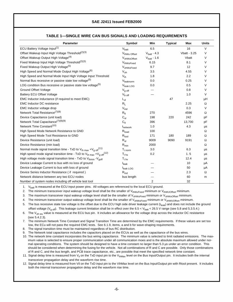
TABLE 1—SINGLE WIRE CAN BUS SIGNALS AND LOADING REQUIREMENTS
Parameter Symbol Min Typical Max Units
ECU Battery Voltage Input(1)
1. Vbatt is measured at the ECU input power pins. All voltages are referenced to the local ECU ground.
Vbatt 6.5 16 V
Offset Wakeup Input High Voltage Threshold(2)(3)
2. The minimum transceiver input wakeup voltage level shall be the smaller of VihWuFixed minimum or VihWUOffset minimum.
3. The maximum transceiver input wakeup voltage level shall be the smaller of VohWuFixed minimum or VohWuOffset minimum.
VihWu Offset Vbatt - 4.3 Vbatt - 3.25 V
Offset Wakeup Output High Voltage(4)
4. The minimum transceiver output wakeup voltage level shall be the smaller of VohWuFixed minimum or VohWUOffset minimum.
VohWuOffset Vbatt - 1.6 Vbatt V
Fixed Wakeup Input High Voltage Threshold(2)(3) VihWuFixed 6.15 8.1 V
Fixed Wakeup Output High Voltage(5)
5. The bus recessive state low voltage is the offset due to the ECU high side driver leakage current (Ileak) and does not include the ground
offset voltage (Vg off). This leakage current limitation shall be in effect over the 6.5 < Vbatt < 26.5 V range (see 5.8 and 5.3.5.4.)
VohWuFixed 9.7 12 V
High Speed and Normal Mode Output High Voltage(6)
6. The Voh wu value is measured at the ECU bus pin. It includes an allowance for the voltage drop across the inductor DC resistantce
(see 5.4.2.3).
Voh 3.5 4.55 V
High Speed and Normal Mode Input High Voltage Input Threshold Vih 1.8 2.2 V
Normal Bus recessive or passive state low voltage(5) Vleaknorm 0.0 0.25 V
LOG condition Bus recessive or passive state low voltage(5) Vleak LOG 0.0 0.5 V
Ground Offset Voltage Vg off — 0.8 V
Battery ECU Offset Voltage Vb off — 1.0 V
EMC Inductor inductance (if required to meet EMC) Lul 47 µH
EMC Inductor DC resistance RL 2.25 ΩEMC Inductor voltage drop Vind 0.3 V
Network Total Resistance(7)(8)
7. The minimum Network Time Constant and Signal Transition Time are determined by the EMC requirements. If these values are set too low, the ECu will not pass the required EMC tests. See 6.1.9, items, a and b for wave-shaping requirements.
8. The signal transition time must be maintained regardless of bus RC distribution.
Rtl 270 4596 ΩDevice Capacitance (unit load) Cul 198 220 242 pF
Network Total Capacitance(7)(8)(9)
9. The Network total capacitance includes the capacitors placed on the ECUs as well as the capacitance of the bus wires.
Ctl 396 13,700 pF
Network Time Constant(10)
10. The network time constant incorporates the bus wiring capacitance. The minimum value is selected to limit radiated emissions. The max-imum value is selected to ensure proper communication under all communication moes and is the absolute maximum allowed under nor-mal operating conditions. The system should be designed to have a time constant no larger than 5.3 µs under an error condition. This should be considered when determining the fusing for the vehicle. Not all combinations of R and C are possible. Only those combinations of R and C, and the bus length, and PCB trace capacitance, etc., are possible that meet the specified network time constant.
tnetwork 1.0 4.3 µs
High Speed Mode Network Resistance to GND Rload 100 ΩHigh Speed Mode Tool Resistance to GND Rtool 171 180 189 ΩDevice Resistance (unit load) Rul 9009 9090 9191 ΩDevice Resistance (min load) Rmin 2000 ΩNormal mode signal transition time - TxD to Vih max +Vg off
(11)
11. Signal delay time is measured from Vil on the TxD input pin to the VihMax level on the Bus Input/Output pin. It includes both the internal
transceiver propagation delay and the waveform rise time.
Tt norm 3.0 6.3 µs
High speed mode signal transition time - TxD to Vih max +Vg off(12)
12. Signal delay time is measured from Vil on the TxD input pin to the VihMax level on the Bus Input/Output pin with Rtool present. It includes both the internal transceiver propagation delay and the waveform rise time.
Tt hs 0.2 1. 5 µs
High voltage mode signal transition time - TxD to Vihmin -Vgoff Tt hv 12.4 µs
Device Leakage Current to bus with no loss of ground Ileak — 10 µA
Device Leakage Current to bus with loss of ground Ileak LOG — 50 µA
Device Series Inductor Resistance ( if required ) Rind — 2.3 ΩNetwork distance between any two ECU nodes bus length — 60 m
Number of system nodes including off vehicle test tool 2 32
SAE J2411 Issued FEB2000
-7-
5.3.3 ECU SELECTIVE AWAKE—This bus includes a selective node wakeup capability which allows normalcommunication to take place among some nodes while leaving the other nodes in an undisturbed sleepstate. This is accomplished by controlling the signal voltages such that all nodes must wake up when theyreceive a higher voltage message signal waveform. The communication system communicates to the nodesinformation as to which nodes are to stay operational (awake) and which nodes are to put themselves into anon communicating low power “sleep” state. Communication at the lower, normal voltage levels shall notdisturb the sleeping nodes. The recommended method of power moding of serial communications nodesshall be by use of the network sleep mode.
The High Speed and High Voltage wakeup features shall not be active at the same time. This requires thatthe bus be awakened only when in the normal speed mode.
5.3.4 CAN CONTROLLER CLOCK TOLERANCE—All nodes which operate on the Single Wire CAN bus shall utilize aCAN controller with a bit timing clock tolerance of ±0.35% to ensure that the CAN bit timing synchronizationshall not be affected by the waveform rise and fall times. See Appendix A for bit timing analysis.
5.3.5 BUS ELECTRICAL PARAMETERS—This section describes two possible modes of the bus electrical voltage levelparameters required by devices which drive and receive signals on the single wire bus. They are the normaland the wakeup communications signal levels. See Table 1. The high level signals (Voh, Vih, Voh wu, andVih wu ) of Table 1 are considered to be the dominant or driven-to-high-voltage bus states.
5.3.5.1 Normal Mode Transmit and Receive Voltage Thresholds for Data Communication—Serial communicationshall operate with normal signal voltage levels indicated in Table 1 without generating a wakeup interruptto the ECU’s controller.
5.3.5.2 High Speed Mode Transmit and Receive Signal Voltages—The high speed input threshold and outputsignal voltages are the same as the normal mode signals. See Table 1.
The High Speed and High Voltage Wakeup bus signals shall not be active at the same time.
High speed operation dominant bus symbols shall not exceed the transceiver duty cycles, operatingvoltage, and temperature requirements as specified in Section 5. (See 5.1.11.)
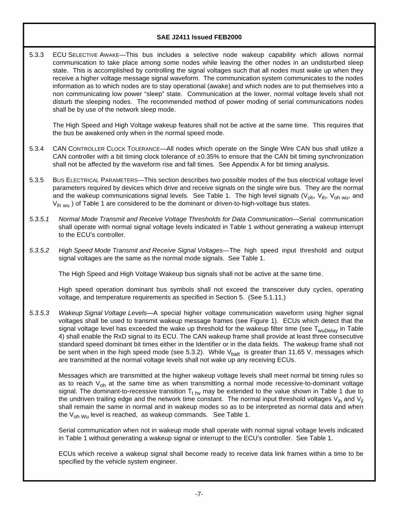
5.3.5.3 Wakeup Signal Voltage Levels—A special higher voltage communication waveform using higher signalvoltages shall be used to transmit wakeup message frames (see Figure 1). ECUs which detect that thesignal voltage level has exceeded the wake up threshold for the wakeup filter time (see TwuDelay in Table4) shall enable the RxD signal to its ECU. The CAN wakeup frame shall provide at least three consecutivestandard speed dominant bit times either in the Identifier or in the data fields. The wakeup frame shall notbe sent when in the high speed mode (see 5.3.2). While Vbatt is greater than 11.65 V, messages whichare transmitted at the normal voltage levels shall not wake up any receiving ECUs.
Messages which are transmitted at the higher wakeup voltage levels shall meet normal bit timing rules soas to reach Voh at the same time as when transmitting a normal mode recessive-to-dominant voltagesignal. The dominant-to-recessive transition Tt hv may be extended to the value shown in Table 1 due tothe undriven trailing edge and the network time constant. The normal input threshold voltages Vih and Vilshall remain the same in normal and in wakeup modes so as to be interpreted as normal data and whenthe Voh Wu level is reached, as wakeup commands. See Table 1.
Serial communication when not in wakeup mode shall operate with normal signal voltage levels indicatedin Table 1 without generating a wakeup signal or interrupt to the ECU’s controller. See Table 1.
ECUs which receive a wakeup signal shall become ready to receive data link frames within a time to bespecified by the vehicle system engineer.
SAE J2411 Issued FEB2000
-8-
FIGURE 1—SINGLE WIRE DOMINANT BIT WAVEFORM
Single wire data link voltage levels and trip points:
a. Voh wu min—Wakeup Output High Voltage—The minimum guaranteed output voltage high level whencommanding all nodes to wak up from sleep mode.
b. Vih wu min—Wakeup Input High Voltage—The minimum guaranteed input voltage high level which willcause the receiving node to wake up from sleep mode.
c. Voh max—Normal Mode Maximum Output High Voltage—The guaranteed maximum output voltage.This will assure that sleeping nodes will not be awakened by normal data voltage levels.
d. Voh min—Normal Mode Minimum Output High Voltage—The guaranteed minimum output voltage toassure that receiving nodes will decode a dominant data link symbol.
e. Vih min—Normal Mode Inptu High Voltage—The minimum input voltage that will be interpreted as adominant data link symbol.
f. Vleak max—Bus Passive State Low Voltage—The maximum bus voltage due to transceiver bus out pinleakage when in the off state.
g. Vg off max—The maximum bus offset voltage due to ground wire variations among ECUs.h. Tt max—Signal Transition Time—The rise or fall time of the data link waveform.
5.3.5.4 Bus Passive State Voltage Offset (Vleak)—The bus input/output circuit shall operate under the followinglimitations:
NOTE—This circuit shall only source current to the bus.
a. When a node is awake and the bus is in the recessive state, the absolute maximum value of Vleakwhich may be provided by the node output current shall be as shown in Table 1 over the bus loadresistance range 100 < Rtl < 9.19 kΩ
b. In the sleep mode without a loss of ground, the node leakage current shall be as shown in Table 1.c. In any node or bus state, the contribution to bus leakage current by any node which has a loss of
ground condition, shall be as specified in Table 1.
SAE J2411 Issued FEB2000
-9-
5.4 Network Topology
5.4.1 LOSS OF ECU GROUND—The loss of ground by any single ECU, with or without an accompanying loss ofVbatt , shall not cause any bus voltage offset that will disable normal communications (See Table 1).
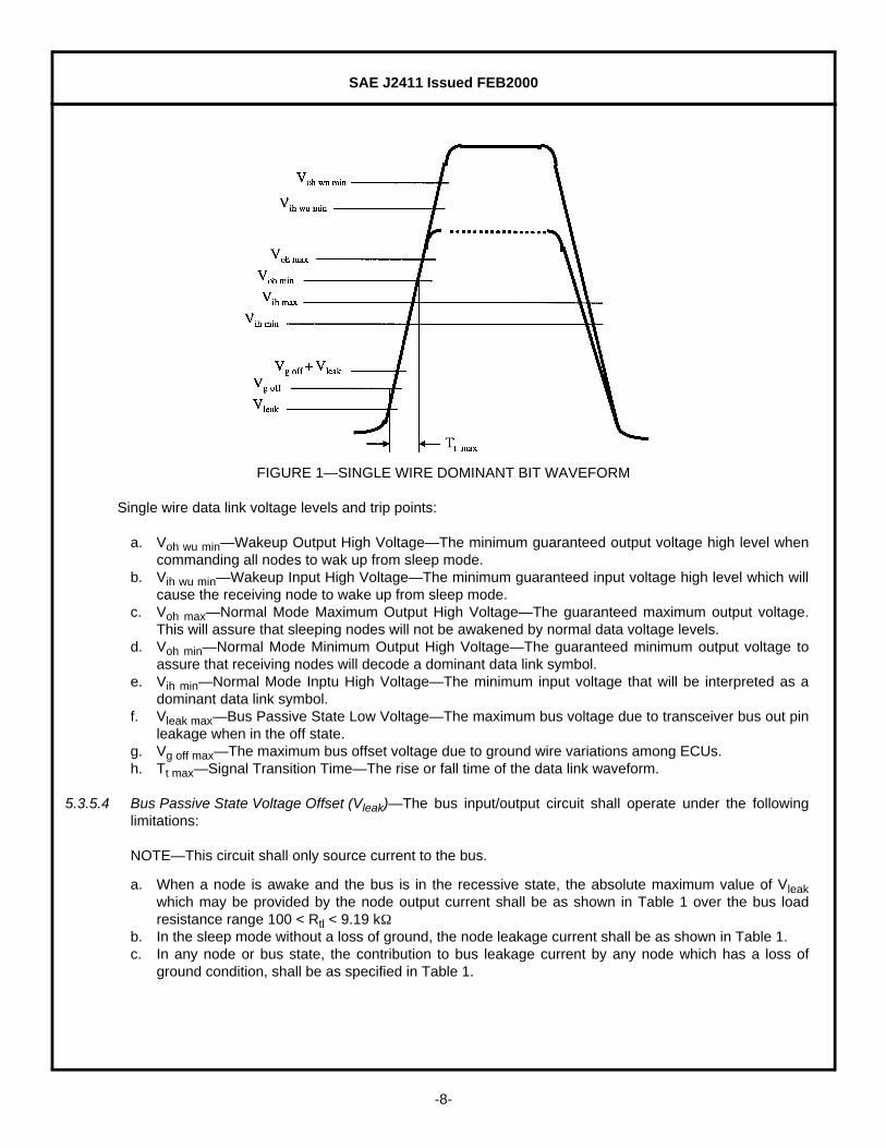
5.4.1.1 Preferred Loss of Ground Protection Method—This shall be accomplished by including a loss of groundprotection circuit in each ECU which will disconnect the path from the bus to Vbatt when a loss of groundoccurs.
This is the preferred method of loss of ground protection. The Single Wire CAN transceivers as specifiedin this document shall provide the ground path interrupt circuit.
This method consists of a provision of a circuit within the ECU which will open the ECU ground path to thebus in the event of a loss of ground condition in the ECU. See Figures 2 and 3. The circuit shall not allowthe ECU to exceed the maximum ECU bus leakage current (Vleak) when in the loss of ground failurecondition. Since this circuit will contribute a bus offset in the normal or non-failed mode, it shall be capableof sinking the maximum load current allowed by the bus load resistor selected for that ECU without causingthe bus voltage to increase to more than the maximum allowed bus offset voltage when there is no loss ofground.
FIGURE 2—SINGLE WIRE DATA LINK PHYSICAL LAYER
FIGURE 3—INTERRUPT METHOD FOR LOSS OF GROUND PROTECTION
SAE J2411 Issued FEB2000
-10-
The transceiver’s loss of ground protection circuit connection to ground shall not be interrupted when theECU ground is intact and the ECU is in the sleep mode. To accomplish this, all nodes shall maintain Vbatton the transceiver at all times when any serial communication can take place. This is to ensure that theunit resistive loads shall not be removed from the network timing circuit.
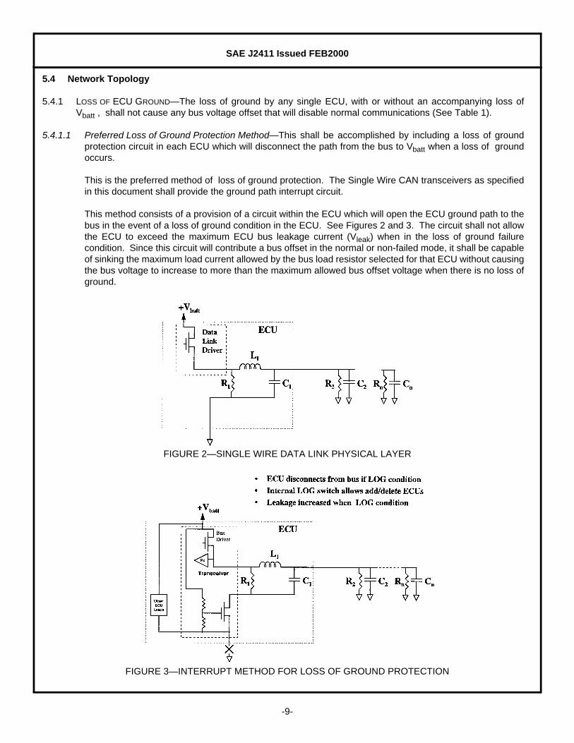
5.4.1.2 Alternative Loss of Ground Protection Methods—The loss of an ECU ground causes the ECU to sourceVbatt through the various ECU circuits to the communications bus instead of to the vehicle system groundas shown in Figures 4 and 5. The equivalent circuit is shown in Figure 5. This shows the effect of busresistance in circuits which have experienced a loss of ground. The objective in these circuits is to makethe Rleak node value high compared to the parallel equivalent resistance of the remaining nodes. Thistends to keep the bus voltage offset sufficiently low to keep from continually sensing a dominant highvoltage. The bus offset voltage due to the node leakage (loss of ground path + high side transmitter driveroff state leakage) must be low enough to allow for a reasonable ground offset voltage and signal noisemargin to keep the bus below the Vih state when the bus is in the recessive state.
FIGURE 4—BUS VOLTAGE OFFSET SOURCES
FIGURE 5—LOSS OF GROUND EQUIVALENT CIRCUIT
These methods do not require the ground interrupt circuit but they do require that each vehicleconfiguration be uniquely designed to assure that the loss of an ECU ground shall not inhibitcommunication among the remaining ECUs.

SAE J2411 Issued FEB2000
-11-
a. All vehicles are designed with enough unit loaded ECUs so that the loss of a single ECU ground shallnot exceed the maximum allowable bus offset voltage contribution by the failed ECU. This requiresthat Rtotal << Rleak. The bus noise margin will be reduced when a node loses ground.
b. Establishing a special primary or concentrated bus load(s) with R and C values chosen so as to limitthe bus offset voltage in the event of a loss of ground condition within an ECU with a considerablyhigher resistance, to less than the maximum allowable bus offset voltage contribution by the failedECU. Again this requires that Rtotal << Rleak. Therefore the primary node(s) resistance must be smallcompared with any node which could lose its ground. It is usually specified as some number of unitnodes as though wired in parallel - where N is the maximum number of possible nodes. The bus noisemargin will be reduced by 1/N when a non-primary node loses ground. The primary bus load musthave a redundant or single point fail-proof ground scheme.
5.4.2 BUS ELECTRICAL LOAD DISTRIBUTION—Each ECU shall contain at least one unit device capacitance load andthe series inductance (if required for EMI Immunity). See Figure 6.
The total network equivalent minimum resistance (Rtl) and maximum capacitance (Ctl) shall comply with thetotals specified in Table 1.
5.4.2.1 Resistor—The unit load resistor shall be as specified in Table 1 and Figure 6 with power rating appropriateto a maximum loaded network under worst case environmental and electrical conditions.
FIGURE 6—TYPICAL SINGLE WIRE CAN BUS INTERFACE
5.4.2.2 Capacitor—The unit load capacitor shall be as specified in Table 1 and Figure 6 with voltage ratingappropriate to a maximum loaded network under worst case environmental and electrical conditions.

SAE J2411 Issued FEB2000
-12-
5.4.2.3 Inductor—An inductor (typical 47 µH), if required by the ECU to meet EMI susceptibility requirements, shallbe placed between the Single Wire CAN device and the load capacitor. The DC series resistance of thisinductor shall as specified in Table 1. The unit load inductor shall be as specified in Table 1 with a powerdissipation rating appropriate to a maximum loaded network under worst case environmental and electricalconditions.
If the inductor is not needed in a particular application, it is recommended that a zero ohm resistor beinstalled in the circuit at the inductor pc board location as a means of later installing the inductor for thosevehicles and transceivers that may need the inductor.
5.4.3 ESD IMMUNITY—The ECU CAN_Bus I/O pin shall withstand the following electrostatic discharges without anydamage to the ECU when subjected to the SAE J1113/13 - Electrostatic Discharge Immunity Test. Theparticular vehicle manufacturer’s ECU component technical specification shall state the Criticality Level of thedevice. See 5.4.4. If the component technical specification does not specify the ESD level, use the Table 2.
5.4.4 ESD TRANSIENT SUPPRESSOR—If necessary, a circuit element such as a transorb (back-to-back zener) or avaristor device may be added to the network in one or more places to provide ESD protection. However,when these devices are used, they may add capacitance or introduce voltage and/or temperature variabilityto the network time constant. When such devices are used, they shall not affect the total bus capacitancelimit or RC time constant. See Figure 6.
If a central ESD suppressor is used, it should be located at or near the Diagnostic Link Connector (DLC) andbetween the DLC and any ECU.
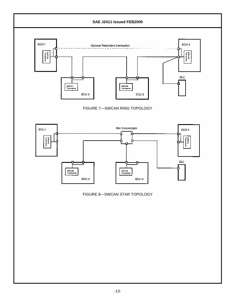
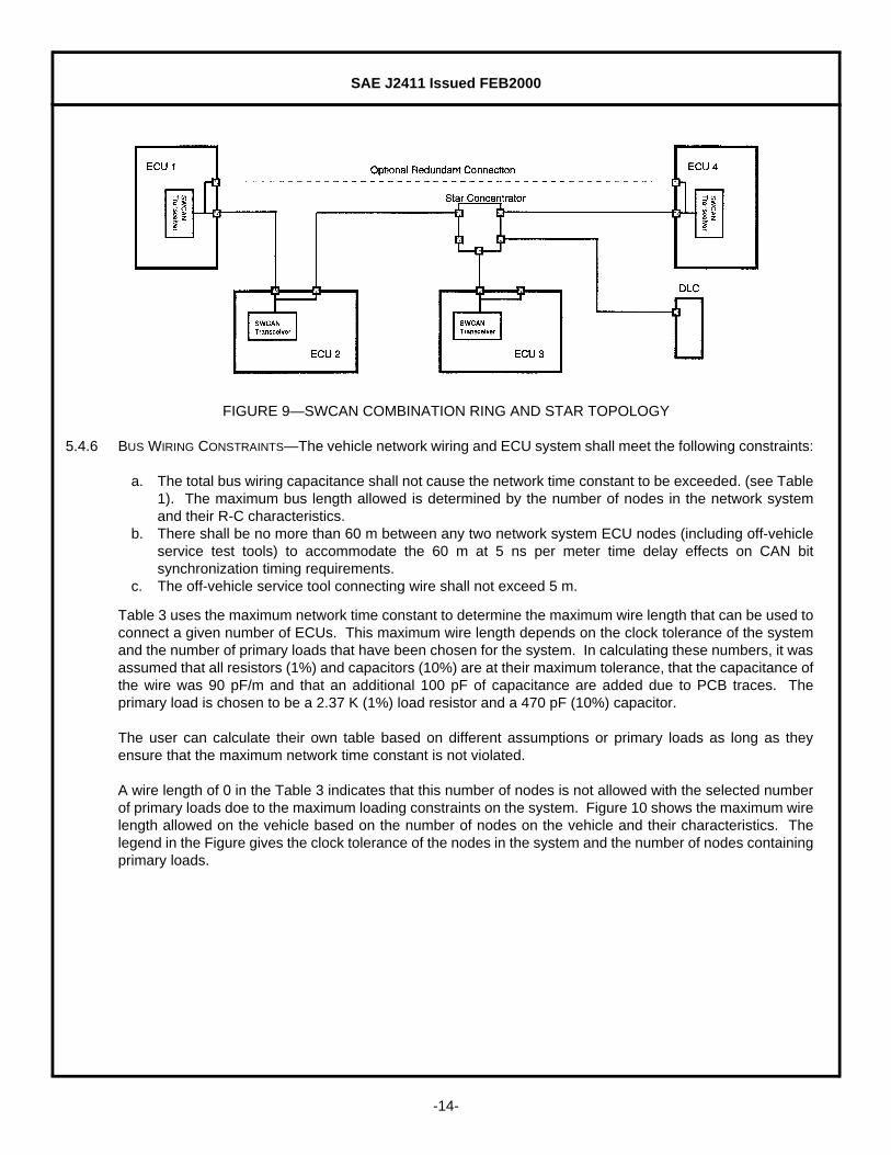
5.4.5 BUS WIRING TOPOLOGY CONFIGURATIONS—The data link physical medium wiring mechanization can beimplemented in any of the following ways:
a. Vehicles may be wired in a ring, a star, or a combination of both. Note that ECUs which are intendedfor use across multiple platforms, may have two connector pins as shown in Figure 7 to allow a ringconnection.
b. The pins of the ECU when applied in a ring, shall be adjacent and in the same connector, shortedtogether as close to the connector as possible, and share EMC and/or loading components.
c. If in a star configuration, the ECU requires only one pin for Single Wire CAN.
The topology of the single wire bus shall be determined for each vehicle platform based on the vehicle’s faulttolerance, serviceability, and bus length requirements. A second bus wire connector terminal for the singlewire CAN circuit at each ECU allows for implementation of a ring configuration, although it is not requiredthat both terminals be used. A ring, star, or combination of ring and star configuration is acceptable as longas all other single wire CAN wiring requirements are met. Illustrations of the single wire CAN topologies areshown in Figures 7, 8 and 9.
TABLE 2—ECU ESD TEST LEVELS
ECU Condition Contact Air (non-Contact)
Unpowered ± 8 kV ±12 kV
Powered ± 8 kV ±15 kV
SAE J2411 Issued FEB2000
-13-
FIGURE 7—SWCAN RING TOPOLOGY
FIGURE 8—SWCAN STAR TOPOLOGY
SAE J2411 Issued FEB2000
-14-
FIGURE 9—SWCAN COMBINATION RING AND STAR TOPOLOGY
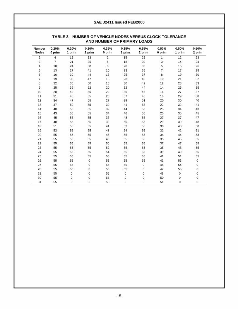
5.4.6 BUS WIRING CONSTRAINTS—The vehicle network wiring and ECU system shall meet the following constraints:
a. The total bus wiring capacitance shall not cause the network time constant to be exceeded. (see Table1). The maximum bus length allowed is determined by the number of nodes in the network systemand their R-C characteristics.
b. There shall be no more than 60 m between any two network system ECU nodes (including off-vehicleservice test tools) to accommodate the 60 m at 5 ns per meter time delay effects on CAN bitsynchronization timing requirements.
c. The off-vehicle service tool connecting wire shall not exceed 5 m.
Table 3 uses the maximum network time constant to determine the maximum wire length that can be used toconnect a given number of ECUs. This maximum wire length depends on the clock tolerance of the systemand the number of primary loads that have been chosen for the system. In calculating these numbers, it wasassumed that all resistors (1%) and capacitors (10%) are at their maximum tolerance, that the capacitance ofthe wire was 90 pF/m and that an additional 100 pF of capacitance are added due to PCB traces. Theprimary load is chosen to be a 2.37 K (1%) load resistor and a 470 pF (10%) capacitor.
The user can calculate their own table based on different assumptions or primary loads as long as theyensure that the maximum network time constant is not violated.
A wire length of 0 in the Table 3 indicates that this number of nodes is not allowed with the selected numberof primary loads doe to the maximum loading constraints on the system. Figure 10 shows the maximum wirelength allowed on the vehicle based on the number of nodes on the vehicle and their characteristics. Thelegend in the Figure gives the clock tolerance of the nodes in the system and the number of nodes containingprimary loads.
SAE J2411 Issued FEB2000
-15-
TABLE 3—NUMBER OF VEHICLE NODES VERSUS CLOCK TOLERANCEAND NUMBER OF PRIMARY LOADS
NumberNodes
0.20%0 prim
0.20%1 prim
0.20%2 prim
0.35%0 prim
0.35%1 prim
0.35%2 prim
0.50%0 prim
0.50%1 prim
0.50%2 prin
2 4 18 33 2 15 28 1 12 233 7 21 35 5 18 30 3 14 244 10 24 38 8 20 33 5 16 265 13 27 41 10 23 35 7 17 286 16 30 44 13 25 37 8 19 307 19 33 47 15 28 40 10 21 328 22 36 50 18 30 42 12 23 339 25 39 52 20 32 44 14 25 3510 28 42 55 22 35 46 16 27 3711 31 45 55 25 37 48 18 29 3812 34 47 55 27 39 51 20 30 4013 37 50 55 30 41 53 22 32 4114 40 53 55 32 44 55 23 34 4315 43 55 55 34 46 55 25 35 4516 45 55 55 37 48 55 27 37 4717 48 55 55 39 50 55 29 39 4818 51 55 55 41 52 55 30 40 5019 53 55 55 43 54 55 32 42 5120 55 55 55 45 55 55 34 44 5321 55 55 55 48 55 55 35 45 5522 55 55 55 50 55 55 37 47 5523 55 55 55 52 55 55 38 48 5524 55 55 55 54 55 55 39 49 5525 55 55 55 55 55 55 41 51 5526 55 55 0 55 55 55 43 53 027 55 55 0 55 55 0 45 54 028 55 55 0 55 55 0 47 55 029 55 0 0 55 0 0 48 0 030 55 0 0 55 0 0 50 0 031 55 0 0 55 0 0 51 0 0

SAE J2411 Issued FEB2000
-16-
FIGURE 10—NUMBER NODES/CLOCK TOLERANCE/PRIMARY LOADS VERSUS WIRE LENGTH CHART
5.4.7 BUS WIRING PRACTICES TO IMPROVE EMC PERFORMANCE
a. Avoid routing bus wire signals with noisy (e.g., injector drivers) and sensitive (e.g., low signal levelsensors, antenna feeds) circuits.
b. Precaution shall be taken when routing signals near antennae or antenna amplifiers to preventinducing noise into these circuits. A shielded wire may be needed near an active antenna.
c. Avoid wire loops by locating bus wires close to the vehicle’s metal ground plane or route a ground wirewith the bus wire.
d. Route the ECUs DC power return wire parallel to the bus wire.
5.4.8 BUS WIRING HARNESS AND ECU CONNECTORS
a. Environmental conditions (temperature, humidity, moisture, and vibration) experienced by the wireconnection system, resistance requirements over the life of the vehicle, as well as terminal designshall be considered when selecting the appropriate terminal plating.
b. Recommended connectors shall have less than 50 mΩ resistance over total vehicle life. c. Wiring harnesses and connectors shall not degrade the signal voltages between any system
transmitting and any receiving node.

SAE J2411 Issued FEB2000
-17-
5.5 Radiated EMI protection—The Single Wire CAN physical layer, when incorporated into an ECU design, shallfunction as specified in the ECU’s intended electromagnetic environment. Additionally, the electromagneticemissions produced during Single Wire CAN related operations shall not interfere with the normal operation ofother ECU’s or subsystems.
Testing using the SAE EMC series of tests listed as follows or equivalent methods, can be used to assess and/or compare the EMC performance of a Single Wire CAN physical layer design. Recommended testingmethods include the following EMC test specifications.
SAE J1113-41—Radiated EmissionsSAE J1113-4—Immunity to Radiated Electric Fields - ECU Bulk Current InjectionSAE J1113-27—Immunity to Radiated Magnetic Fields - Reverberation Method
Formal validation of the CAN physical layer design using these or other acceptance criteria for any given ECUshall be specified by the vehicle manufacturer.
5.6 Fault Tolerant Modes—The Network shall meet the requirements as defined per the following failure modes:
a. ECU Power Loss—ECUs shall not interfere with normal communication among the remaining busECUs during a loss of power (or low voltage) condition. Upon return of power, normal operation shallresume without any operator intervention within a time determined by the vehicle manufacturer.
b. Bus Wiring Short to Ground—Network data communications may be interrupted but there shall be nodamage to any ECU when the bus is shorted to ground. A network impedance of less than 50 Ωbetween the bus and ground shall be considered a short to ground and continued communications arenot guaranteed or required. Upon removal of the fault, normal operation shall resume without anyoperator intervention within a time determined by the vehicle manufacturer.
c. Bus Wiring Short to Battery—Network data communications may be interrupted but there shall be nodamage to any device when the bus is shorted to positive battery less than 18 V (Vbatt < 18 V). Anetwork impedance of less than 50 Ω between the bus and battery shall be considered a short andcontinued communications are not guaranteed or required. Upon removal of the fault, normaloperation shall resume without any operator intervention within a time determined by the vehiclemanufacturer.
d. Loss of ECU Wiring Connection to Ground—When an ECU loses its ground connection, it shall notprevent the remaining ECUs from normal communication. The ECU shall implement this protection byopening the ground path to the bus load resistor when a loss of ground occurs. See 5.4.1.
e. A short or open in any single wiring circuit of an ECU, except for power, ground, or serial data, shall notpreclude the ability to communicate with that ECU for diagnostic purposes.
5.7 Ground Offset Voltage—Ground offset voltage limits at the ECU as specified in Table 1 must be maintainedover the entire range of 6.5 < Vbatt < 26.5 V.
5.8 Operating Battery Power Voltage Range
5.8.1 NORMAL BATTERY VOLTAGE POWER OPERATION—Unless otherwise specified by the Component TechnicalSpecification, ECUs shall be capable of meeting all requirements specified in this document when the VbattECU voltage as measured at the ECU power input pin is within the range of 6.5 to 16 V DC. The ECU shallprovide Vbatt IC to the bus transceiver within the range of 5.5 to 16 V (see 6.1.10).

SAE J2411 Issued FEB2000
-18-
5.8.2 BATTERY POWER OVERVOLTAGE OPERATION—For message frames which must occur at higher batteryvoltage conditions, some means of clamping Vbatt may be required to allow communications to operate inthe 6.5 < Vbatt ECU < 26.5 V range.
a. Recessive state transceiver leakage current limits shall be maintained over this range. b. Communication shall not be disturbed by any node over this range. c. ECUs shall not sustain permanent damage when subjected to Vbatt ECU up to 26.5 V.d. ECU must limit Vbatt ECU transients of greater than 40 V and/or duration greater than 10 ms.
5.8.3 LOW BATTERY VOLTAGE OPERATION
a. For Vbatt ECU < 2.5 V, the bus shall be passive (not be driven dominant) and RxD shall be undriven(high).
b. For 2.5 < Vbatt ECU < 6.5 V the bus may operate in either the normal or the passive mode as definedpreviously.
5.8.4 BATTERY OFFSET VOLTAGE—The battery offset voltage between the battery input pins of any ECU limitsspecified in Table 1 must be maintained over the entire range of 6.5 < Vbatt ECU < 26.5 V.
5.8.5 REVERSE BATTERY BLOCKING DIODE—The reverse battery blocking diode voltage drop between the ECU’sVbatt ECU input pin and the transceiver’s Vbatt IC input pin shall be Vdiode < 1.0 V.
5.9 Environmental Requirements—ECU environmental requirements shall be specified in the individual ECUComponent Technical Specifications which call out this specification. In general, communications deviceswhich are installed in these ECUs shall operate in the –40 to +125 °C temperature range.
6. Single Wire CAN Transceiver Specification—When the physical layer transceiver circuitry is implementedas a standalone integrated circuit, it shall conform to the package specifications given in this section. Alternatetransceiver circuit provisions are allowed provided that the CAN_Bus input/output and the Bus Load circuitsmust operate as specified in 6.1.7 and 6.1.9).
6.1 Transceiver Pin Descriptions—The transceiver may be supplied in either an 8 or a 14 pin Small OutlineIntegrated Circuit package (SOIC) as shown in Figures 11 and 12. Pin functional descriptions are shown asfollows.
FIGURE 11—SINGLE WIRE CAN TRANSCEIVER IN 8 PIN SOIC PACKAGE

SAE J2411 Issued FEB2000
-19-
FIGURE 12—SINGLE WIRE CAN TRANSCEIVER 8 PIN OR 14 PIN SOICPACKAGE PIN ASSIGNMENTS
6.1.1 GND PIN—GROUND—Some 8 pin transceivers may require additional pc board surface or ground plane as aheat conductor to meet thermal requirements. See individual transceiver supplier SWC transceiverspecifications.
6.1.2 TXD INPUT PIN—Logic command to transmit on the single wire CAN bus as follows:
a. TxD Polarity
1. TxD = logic 1 (or floating) on this pin shall produce an undriven or recessive bus state (low busvoltage).
2. TxD = logic 0 on this pin shall produce either a bus normal or a bus high voltage dominant statedepending on the transceiver mode state (high bus voltage).
3. If the TxD pin is driven to a logic low state while the Mode 0,1 pins are in the 0,0 or sleep state, thetransceiver shall not drive the CAN_Bus pin to the dominant state.
b. For transceivers which do not limit the TxD input current sufficiently to prevent latchup, the ECU shallprovide a weak (approximately 10 kΩ) external pulled-up-to-Vcc resistor on the TxD pin which willcause the transmitter to default to the bus recessive state when TxD is not driven.
c. TxD input signals shall be standard CMOS logic levels:
1. Vil max < 1.6 V2. Vih min > 3.4 V
6.1.3 MODE 0 AND MODE 1 INPUT PINS—The Mode 0 and Mode 1 pins are used to select transceiver operatingmodes:
a. Mode 0 = 0, Mode 1 = 0 - Sleep mode. Transceiver is in low power state, waiting for wake up via highvoltage signal or by mode pins change to any state other than 0,0. In this state, the CAN_Bus pin shallnot be in the dominant state regardless of the state of the TxD pin. See 6.1.4.
b. Mode 0 = 1, Mode 1 = 0. High Speed mode.c. Mode 0 = 0, Mode 1 = 1. Transmit with high voltage signals to wake up remote nodes.d. Mode 0 = 1, Mode 1 = 1. Normal speed and signal voltage mode.e. The transceiver shall provide a weak internal pulled down to ground resistor on each of these pins
which causes the transceiver to default to sleep mode when they are not driven.

SAE J2411 Issued FEB2000
-20-
f. The Mode 0, 1 input signals shall be standard CMOS logic levels:g. Vil max < 1.6 Vh. Vih min > 3.4 V
6.1.4 RXD OUTPUT PIN—LOGIC DATA AS SENSED ON THE SINGLE WIRE CAN BUS
a. RxD polarity
1. RxD = logic 1 on this pin shall indicate a bus recessive state (low bus voltage).2. RxD = logic 0 on this pin shall indicate a bus normal or high voltage bus dominant state.
b. RxD in Sleep Mode
1. RxD shall not pass signals to the micro processor while in sleep mode until a valid wake up busvoltage level is received or the Mode 0,1 pins are not 0,0 respectively. When the valid wake up busvoltage signal awakens the transceiver, it shall pass these signals to the RxD pin. However, if theMode 0 and 1 pins are both at logic 0, the transceiver shall return to the sleep condition when thewake up bus voltage signal is not present.
2. When not in sleep mode all valid bus signals will be sent out on the RxD pin. 3. RxD will be placed in the undriven or off state when in sleep mode.
c. Preferred Operation of RxD in Sleep Mode
1. RxD shall not pass signals to the microprocessor while in sleep mode unless a valid transition from arecessive state to a valid wakeup bus voltage is received or the Mode 0,1 pins are not 0,0respectively. When the valid wakeup bus voltage signal transition awakens the transceiver, it shallpass these bus signals to the RxD pin. However, if the Mode 0 and 1 pins are at logic 0, thetransceiver shall return to the sleep condition no sooner than 150 ms and no later than 1 s from theedge.
2. When not in sleep mode, all valid bus signals will be sent out on the RxD pin. 3. RxD will be placed in the undriven or off state when in sleep mode
d. RxD is an open drain (or collector) output which when pulled up to Vcc shall maintain an output voltageVol (Vsat) < 0.4 V at 2.0 ma minimum. Transceivers may also provide an internal active pull up if it willoperate with the external pull up resistor.
e. RxD Typical Load
a. Resistance: 2.7 kΩb. Capacitance: < 25 pF
6.1.5 VCC IC INPUT PIN = +5 V ± 5%—The total transceiver Vbatt + Vcc quiescent current (IQ = Ibatt + Icc) draw insleep mode shall not exceed the maximum IQ amount specified in Table 4.
When Vcc is not within specified range, the bus shall be passive (not be driven dominant) and RxD shall beundriven (high), regardless of the state of the TxD pin.
6.1.6 RSLEW INPUT PIN—WAVEFORM SLEW CONTROL RESISTOR—Rslew shall be externally pulled high to Vcc throughthe slew control resistor (with resistance value specified by the transceiver manufacturer - typical Rslew value= 100 kΩ at the waveform slope values specified in 6.1.9.)
6.1.7 BUS LOAD INPUT PIN—Resistor ground with internal open-on-loss-of-ground protection
a. When the ECU experiences a loss of ground condition, this pin shall switch to a high impedance state.b. The ground connection through this pin shall not be interrupted in any transceiver operating mode
including the sleep mode. The ground connection shall only be interrupted when there is a valid lossof ground condition.

SAE J2411 Issued FEB2000
-21-
c. This pin shall normally provide the bus load resistor with a path to ground which contributes less than0.1 V to the bus offset voltage when sinking the maximum current through one unit load resistor.
d. The transceiver’s maximum bus leakage current contribution to Vol from the LOAD pin when in a lossof ground state is 50 µA over all operating temperatures and 3.5 < Vbatt < 16 V.
6.1.8 Vbatt IC INPUT PIN—VEHICLE BATTERY VOLTAGE
a. The transceiver shall be fully operational as described in Table 4 over the range 5.5 < Vbatt IC < 16 V asmeasured between the GND pin and this pin.
b. For Vbatt IC < 2.5 V, the bus shall be passive (not be driven dominant) and RxD shall be undriven(high), regardless of the state of the TxD pin.
c. For 2.5 < Vbatt IC < 5.5 V, the bus may operate in either the normal or the passive bus mode as definedpreviously.
d. The transceiver shall operate normally as indicated in Table 4 or maintain the passive state (i.e., shallnot disturb normal communications) when Vbatt IC > 16 V.
e. The transceiver battery current shall be less than 100 µA in the sleep mode.f. At the transceiver Vbatt pin, load dump events of less than 10 ms transients of up to 40 V shall not
cause transceiver damage. Transients greater than 40 V shall be clamped by the ECU.g. The total transceiver Vbatt + Vcc quiescent current draw in sleep mode shall not exceed the maximum
IQ amount specified in Table 4.
6.1.9 CAN_BUS INPUT/OUTPUT PIN
a. Wave Shaping in normal mode—Wave shaping is incorporated into the transmitter to minimize EMIradiated emissions. An important contributor to emissions is the rise and fall times during outputtransitions at the “corners” of the voltage waveform. The resultant waveform shall be one half of a sinewave of frequency 50 to 65 kHz at the rising waveform edge and one quarter of this sine wave at fallingor trailing edge (the waveform shall be in the undriven state for the remainder of the bit time). Thismeans that the waveform rise and fall times shall be at least 3.5 ms each as measured between the 10and 90% of Voh points. The waveform shall remain at constant Voh (or Voh wu) between the rising andfalling edges.
b. Wave Shaping in high speed mode—Wave shaping control of the rising and falling waveform edgesshall be disabled during high speed mode. EMI emissions requirements are waived during this mode.The waveform rise time in this mode shall be less than 1 µs.
c. Short circuits—If the CAN_Bus pin is shorted to ground for any duration of time, an over temperatureshut down circuit shall disable the output high side drive source transistor before the local dietemperature exceeds a damage limit threshold. The output transistor shall remain latched off until thelocal die temperature is 10 to 15 °C below the latch off trip temperature.
d. Leakage—This pin shall not source more than 10 µA over the range of –40 °C < ambient temperature< 125 °C. See 5.8.4 and 5.3.5.4.
e. Transceiver Bus Interface Signals and Loading Requirements - See Table 4.

SAE J2411 Issued FEB2000
-22-
6.1.10 TRANSMIT OPERATING CONDITIONS—Transmit duty cycles:
Assume one transition for each bit time - recessive to dominant (low to high) or dominant to recessive (highto low). Bit timing is 30 µs/bit in normal mode and 12 µs/bit in high speed mode. Assume 50% transmitter ontime as the bit duty cycle during any frame transmissions. The following duty cycle requirements apply overall power and environmental conditions unless otherwise specified. Some 8 pin transceivers may requireadditional pc board surface or ground plane as a heat conductor to meet thermal requirements. Seeindividual supplier SWC transceiver specifications. See Table 1 for details of bus loading and voltageranges.
TABLE 4—TRANSCEIVER BUS INTERFACE SIGNALS AND LOADING REQUIREMENTS
Parameter Symbol Min Typical Max Units
Transceiver Battery Voltage Input(1)
1. Vbatt IC is measured at the transceiver input power pins. All voltages are referenced to the local transceiver ground.
Vbatt IC 5.5 16 V
Offset Wakeup Input High Voltage Threshold(2)(3)
2. The minimum transceiver input wakup voltage level shall be the smaller of VihWuFixed minimum or VihWuOffset minimum.
3. The maximum tranceiver input wakeup voltage level shall be the smaller of VihWuFixed maximum or VihWuOffset minimum.
VihWuOffset Vbatt - 4.3 Vbatt - 3.25 V
Offset Wakeup Output High Voltage(4)
4. The minimum transceiver output wakeup voltage level shall be the smaller of VohWuFixed minimum or VohWuOffset minimum.
Voh wu offset Vbatt - 1.5 Vbatt V
Fixed Wakeup Input High Voltage Threshold(2)(3) VihWuFixed 6.15 8.1 V
Fixed Wakeup Output High Voltage(4) VohWuFixed 9.8 12 V
High Speed and Normal Mode Output High Voltage Voh 3.6 4.55 V
High Speed and Normal Mode Input High Voltage Input Threshold Vih 1.8 2.2 V
Normal Bus recessive or passive state low voltage(4) Vleaknorm/Vol 0.0 0.25 V
LOG condition Bus recessive or passsive state low voltage(5)
5. Bus recessive state low voltage is the offset due to the transceiver high side driver leakage current (lleak) and does not include the ground offset voltage (Vg off). This leakage current limitation shall be in effect over the range 5.5 < Vbatt IC < 26.5 V (see 5.8 and
5.3.5.4.)
VleakLOG/Vol 0.0 0.5 V
LOG switch Voltage (normal operation) VLOG norm 0.1 V
LOG switch Voltage (loss of battery) VLOG err 1 V
Ground offset Voltage Vg off — 0.8 V
Transceiver Battery ECU Offset Voltage Vb off — 1.0 V
Device Resistance (min load) Rmin 2000 Ω
Network Total Resistance Rtl 270 4596 ΩNetwork Total Capacitance Ctl 396 13 700 pF
High Speed Mode network Resistance to GND Rload 100 Ω
Normal Mode Signal Transition Time Tt norm 3.0 6.3 µs
Normal Mode Receive Delay Time Rt norm 0.3 1.0 µs
High Speed Mode Signal Transition Time Tt hs 0.2 1.5 µs
High Speed Mode Receive Delay Time Rt hs 0.2 0.7 µs
High Voltage Mode Signal Transition Time - TxD to Vihmin - Vgoff Tt hv 12.4 µs
Transceiver Leakage Current to Bus with no Loss of Ground Ileak — 10 µA
Transceiver Leakage Current to Bus (one Node with Loss of Ground) Ileak LOG — 50 µA
Transceiver Vbatt + Vcc Quiescent Current in sleep mode with Vbus <
1.5 V
IQ = Ibatt + Icc 100 µA
Transceiver Vbatt + Vcc Quiescent Current in Sleep Mode with Vbus >
1.5 V
IQ = Ibatt + Icc 1 mA
Wakeup Filter Time Delay TwuDelay 5 70 µs
SAE J2411 Issued FEB2000
-23-
a. High speed mode operating requirements
1. Diagnostics Tool—Must transmit frames in high speed mode of 75% bit duty cycle forever. The toolmay utilize the following special operating condition modifications: 9 V ≤ Vbatt ≤ 12.6 V and –40 °C <Ambient Temperature < +85 °C.
2. Vehicle ECUs - Must transmit in high speed at 50% bit duty cycle during continuous frametransmissions for at least 1 s. After 1 s, an over temperature shut down circuit may disable theoutput high side drive source transistor before the local die temperature exceeds a damage limitthreshold. The output transistor shall remain latched off up to 5 s to allow the local die temperatureto reach 10 to 30 °C below the latch off trip temperature.
3. The vehicle ECUs shall be able to transmit forever with 50% bit duty cycle frames being transmittedat a 10% duty cycle of maximum possible bus traffic frames.
b. Normal speed mode operation must transmit frames of 50% bit duty cycle and frame duty cycle of100% forever.
c. High voltage mode operation must transmit frames of 50% bit duty cycle for 1 s and frame duty cycle of10% forever.
6.1.11 TRANSCEIVER MODE CHANGES
a. The transceiver shall perform the mode change without damage regardless of the state or activity onthe bus or on the TxD pin - unless there is a mode change to sleep mode attempt during a wakeuphigh voltage condition on the bus. In this case, the transceiver shall remain in the awake state untilthe wakeup voltage levels are no longer present on the bus.
b. It is the responsibility of the microprocessor to manage any system or ECU effects associated with themode change and to insure that mode changes take place between frames.
c. Times allowed to change transceiver operating modes are:
t < 30 µs in switching from normal to high speed or high voltage modest < 30 µs in switching from high speed or high voltage modes to normal modet < 500 µs when switching from normal to sleep modet < 50 µs when switching from sleep to normal mode
d. It is the responsibility of the transceiver to assure that after a mode change:
1. No lock-up or permanent damage will occur2. After a change to normal mode, no transmitted wake up signals will occur
6.1.12 MAXIMUM TRANSCEIVER PROPAGATION DELAYS
a. Transmitter Delays—Transmitter delays shall be less than 6.3 µs in standard speed mode and 1.5 µsin high speed mode as measured from 90% of the TxD input logic high level to Vih max + Vg off asmeasured at the transceiver CAN Bus I/O pin, with worst case silicon and bus loading componenttolerances.
b. Receiver Delays—Receiver delays shall be less than 1 µs in standard speed mode and 0.7 µs in highspeed mode as measured at the transceiver CAN Bus I/O pin, from Vih max of the normal voltage levelbus dominant trailing edge to 90% of the RxD output logic low waveform with worst case temperatureand Vbatt.
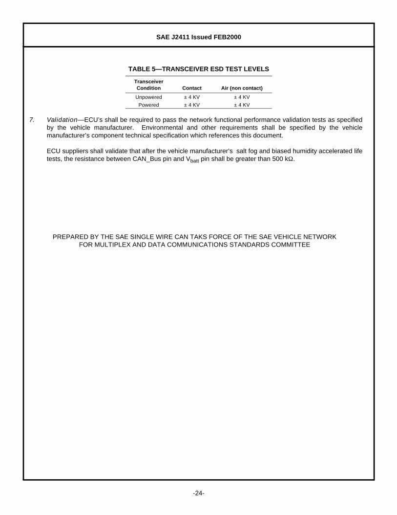
6.1.13 TRANSCEIVER ELECTROSTATIC DISCHARGE IMMUNITY—The transceiver shall withstand the electrostaticdischarges specified in Table 5 to pins which are brought out to an ECU external connector, for example Vbatt,Load, CAN_Bus, without any damage to the transceiver, when subjected to the SAE J1113-13 tests.
SAE J2411 Issued FEB2000
-24-
7. Validation—ECU’s shall be required to pass the network functional performance validation tests as specifiedby the vehicle manufacturer. Environmental and other requirements shall be specified by the vehiclemanufacturer’s component technical specification which references this document.
ECU suppliers shall validate that after the vehicle manufacturer’s salt fog and biased humidity accelerated lifetests, the resistance between CAN_Bus pin and Vbatt pin shall be greater than 500 kΩ.
PREPARED BY THE SAE SINGLE WIRE CAN TAKS FORCE OF THE SAE VEHICLE NETWORKFOR MULTIPLEX AND DATA COMMUNICATIONS STANDARDS COMMITTEE
TABLE 5—TRANSCEIVER ESD TEST LEVELS
TransceiverCondition Contact Air (non contact)
Unpowered ± 4 KV ± 4 KV
Powered ± 4 KV ± 4 KV
SAE J2411 Issued FEB2000
-25-
APPENDIX A
SINGLE WIRE CAN BIT TIMING ANALYSIS
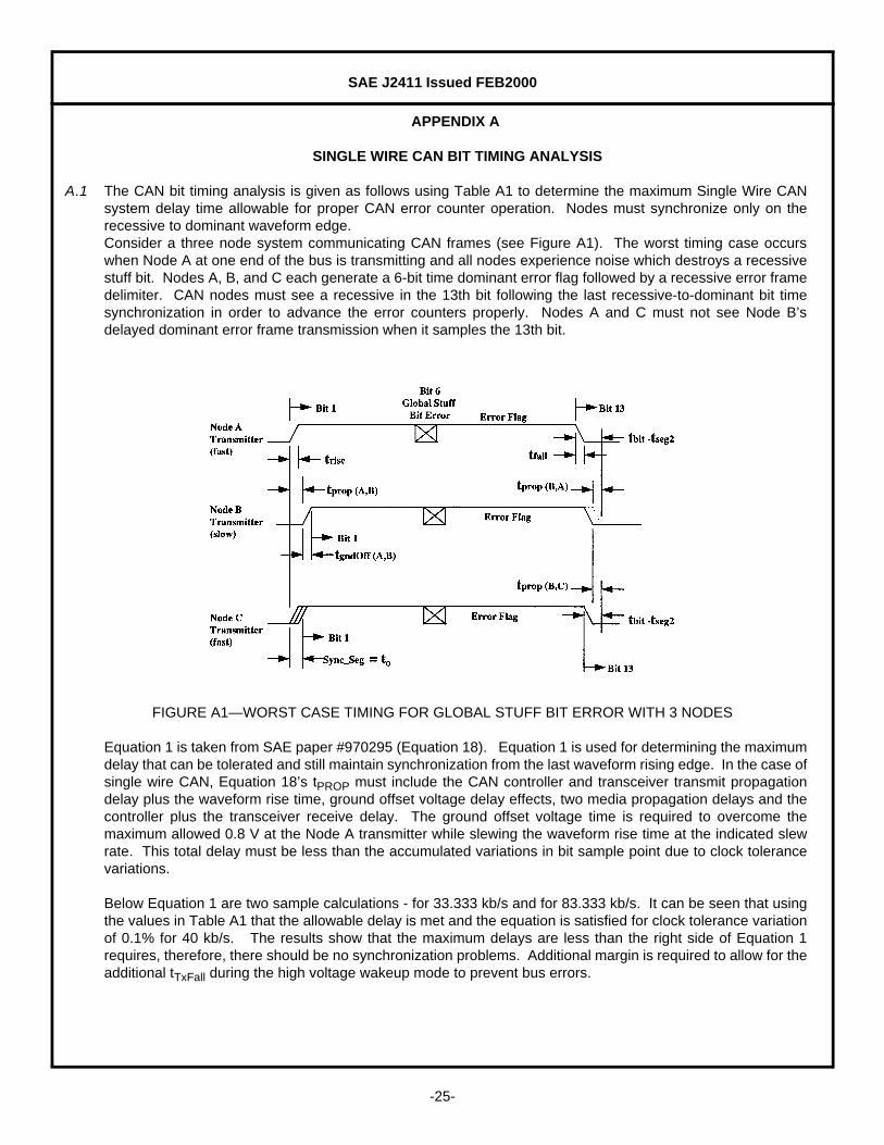
A.1 The CAN bit timing analysis is given as follows using Table A1 to determine the maximum Single Wire CANsystem delay time allowable for proper CAN error counter operation. Nodes must synchronize only on therecessive to dominant waveform edge.Consider a three node system communicating CAN frames (see Figure A1). The worst timing case occurswhen Node A at one end of the bus is transmitting and all nodes experience noise which destroys a recessivestuff bit. Nodes A, B, and C each generate a 6-bit time dominant error flag followed by a recessive error framedelimiter. CAN nodes must see a recessive in the 13th bit following the last recessive-to-dominant bit timesynchronization in order to advance the error counters properly. Nodes A and C must not see Node B’sdelayed dominant error frame transmission when it samples the 13th bit.
FIGURE A1—WORST CASE TIMING FOR GLOBAL STUFF BIT ERROR WITH 3 NODES
Equation 1 is taken from SAE paper #970295 (Equation 18). Equation 1 is used for determining the maximumdelay that can be tolerated and still maintain synchronization from the last waveform rising edge. In the case ofsingle wire CAN, Equation 18’s tPROP must include the CAN controller and transceiver transmit propagationdelay plus the waveform rise time, ground offset voltage delay effects, two media propagation delays and thecontroller plus the transceiver receive delay. The ground offset voltage time is required to overcome themaximum allowed 0.8 V at the Node A transmitter while slewing the waveform rise time at the indicated slewrate. This total delay must be less than the accumulated variations in bit sample point due to clock tolerancevariations.
Below Equation 1 are two sample calculations - for 33.333 kb/s and for 83.333 kb/s. It can be seen that usingthe values in Table A1 that the allowable delay is met and the equation is satisfied for clock tolerance variationof 0.1% for 40 kb/s. The results show that the maximum delays are less than the right side of Equation 1requires, therefore, there should be no synchronization problems. Additional margin is required to allow for theadditional tTxFall during the high voltage wakeup mode to prevent bus errors.

SAE J2411 Issued FEB2000
-26-
SAE #970295 Equation 18:Max. delay - tPropMax < tbit – tseg2 – ∆F (25 tbit – tQ – tseg2) – tQ
(Eq. A1)
EXAMPLE 1—33.333 kb/s 6.3 + 0.2 + 1 + 6.3 + 0.2 + 1 + 0.3 = 15.3 µs ≤ 21.4 µs
EXAMPLE 2—33.333 kb/s (wakeup) 6.3 + 0.2 + 1 + 12.4 + 0.2 + 1 + 0.3 = 21.4 µs ≤ 21.4 µs
EXAMPLE 3—83.333 kb/s 1.5 + 0.2 + 0.7 + 1.5 + 0.2 + 0.7 + 0.3 = 5.1 µs ≤ 7.96 µs
TABLE A1—SWC CAN BIT TIME PARAMETERS
33.333 kb/s 83.333 kb/s
Bit time tbit 30 µs 12 µs
Crystal ( example) 8.00 MHz 8.00 MHz
Clock tolerance Df ±0.35% ±0.35%
tQ ( example) 2.0 µs 1.0 µs
TSEG1 ( example) 11 (12 tq) 8 (9 tq)
TSEG2 ( example) 1 (2 tq) 1 (2 tq)
tseg 1 + tQ 26.0 µs (86.7% Bit time) 10.0 µs (83.33% Bit time)
tseg 2 4.0 µs (13.3% Bit time) 2.0 µs (16.67% Bit time)
tSJW 2 tQ ≤ tseg 2 = 4.0 µs 2 tQ ≤ tseg 2 = 2.0 µs
tprop 0.3 µs (60 m one way) 0.3 µs (60 m one way)
txFall 6.3 µs (12.4 µs HVWU) 1.5 µs
txRise (includes t GNDOffset ) 6.3 µs 1.5 µs
tRxDelay 1 µs 0.7 µs
tTxRiseDelay tprop tRxDelay tTxFall tprop tRxDelay tChokeDelay tbit tseg2– ∆f 25 tbit tQ– tseg2–( )– tQ–<
+ + + + + +

SAE J2411 Issued FEB2000
-27-
APPENDIX B
SINGLE WIRE CAN HIGH SPEED MODE ANALYSIS
B.1 The SWC high speed mode can operate at various maximum bit rates depending on the number of attachednodes. The tool resistance is connected to the bus and this combines with the remaining bus resistors to makea decreasing total bus resistance as more nodes are added. However, because of the tool resistor, the totalbus resistance does not change at the same rate as the total bus capacitance, there is an increasing RC timeconstant on the high speed bus as more nodes are added. This results in a somewhat declining maximumhigh speed bit rate as more nodes are added. High speed tools and vehicle nodes may be programmed to adjust the high speed bit rate according to thenumber of attached nodes or the high speed mode may be fixed according to the maximum number of nodesthe tool is expected to encounter. To minimize the proliferation of high speed operating modes in which thetool and the vehicle ECUs must accommodate, the high speed mode is fixed at 83.333 kbits/s whichcorresponds to the maximum speed allowed at the full 32 node bus loading.
An example calculation set up for the CAN controller to operate at both 33.333 and 83.333 Kbits/s is shown asfollows. Reference Intel 82527 and/or Philips SJA1000 data sheets (other CAN controller suppliers use similarmethods):
(Eq. B1)
where:
CAN Bus Frequency is in bits/secondXTAL = CAN timing oscillator frequencyDSC = Divide System Clock (0 or 1 - divides XTAL by 1 or 2 respectively)BRP = Baud Rate Prescaler (0 to 63)TSEG1 = 2 to 15 - sets the bit sample pointTSEG2 = 1 to 7 - sets the time remaining in the bit after the sample point
Note that in the CAN 2.0 specification, PROP_SEG + PHASE_SEG1 corresponds to TSEG1 andPHASE_SEG2 corresponds to TSEG2.
For the low speed bit rate and the high speed bit rate, the CAN controller configuration and oscillator frequencyare determined by the following conditions/equations:
(Eq. B2)
(Eq. B3)
Once these two conditions are met, the DSC and BRP values can be calculated from Equation B1.
EXAMPLE Solution:
Set Low speed bit rate LSBR = 33 333 bits/sSet High speed bit rate HSBR = 83 333 bits/s
XTAL is chosen as 8 MHz
XTAL / LSBR = 240 (an integer)XTAL / HSBR = 96 (an integer)
CAN Bus Frequency = XTAL / [(DSC + 1) x (BRP + 1) x (3 + TSEG1 + TSEG2)]
XTAL / low speed bit rate( ) and XTAL / high speed bit rate) MUST both be integer numbers
TSEG1 + TSEG2 + 2( ) MUST be a factor of the results of the equations in Equation B2

SAE J2411 Issued FEB2000
-28-
Low Speed:
If:
TSEG1 is choses as 11 (12 –1)TSEG2 is chosen as 1 (2 – 1)
This gives tseg1 = 86.7% of bit time and tseg2 = 13.3% of bit time
Then:
TESG1 + TSEG2 + 3 = 15 = total time quanta per bit
Both conditions are satisfied and DSC and BRP can be calculated by substitution in Equation B1.
For low speed:
DSC = 0BRP = 15
or
DSC = 1BRP = 7
High Speed:
If:
TSEG1 is chosen as 8 (9 –1)TSEG2 is chosen as 1 (2 – 1)
This gives tseg1 = 83.33% of bit time and tseg2 = 16.67% of bit time
Then:
TESG1 + TSEG2 + 3 = 12 = total time quanta per bit
Both conditions are satisfied and DSC and BRP can be calculated by substitution in Equation B1.
For high speed:
DSC = 0BRP = 7
or
DSC = 1
All nodes connected to the Single Wire CAN network must maintain their sample point in the range of 80% oftheir bit time. This implies that there are limited acceptable sets of CAN clock frequencies, tQ and tSEG settingswhich will allow the network to operate properly. Several acceptable example clock frequencies with theirassociated calculated CAN bit settings are shown in the Table B1. Other sets may be possible with carefulanalysis.
SAE J2411 Issued FEB2000
-29-
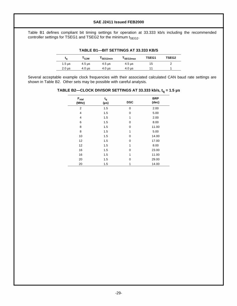
Table B1 defines compliant bit timing settings for operation at 33.333 kb/s including the recommendedcontroller settings for TSEG1 and TSEG2 for the minimum tSEG2.
Several acceptable example clock frequencies with their associated calculated CAN baud rate settings areshown in Table B2. Other sets may be possible with careful analysis.
TABLE B1—BIT SETTINGS AT 33.333 KB/S
tq TSJW TSEG2min TSEG2max TSEG1 TSEG2
1.5 µs 4.5 µs 4.5 µs 4.5 µs 15 2
2.0 µs 4.0 µs 4.0 µs 4.0 µs 11 1
TABLE B2—CLOCK DIVISOR SETTINGS AT 33.333 kb/s, tq = 1.5 µs
Fxtal(MHz)
tq(µs) DSC
BRP(dec)
2 1.5 0 2.00
4 1.5 0 5.00
4 1.5 1 2.00
6 1.5 0 8.00
8 1.5 0 11.00
8 1.5 1 5.00
10 1.5 0 14.00
12 1.5 0 17.00
12 1.5 1 8.00
16 1.5 0 23.00
16 1.5 1 11.00
20 1.5 0 29.00
20 1.5 1 14.00

SAE J2411 Issued FEB2000
-30-
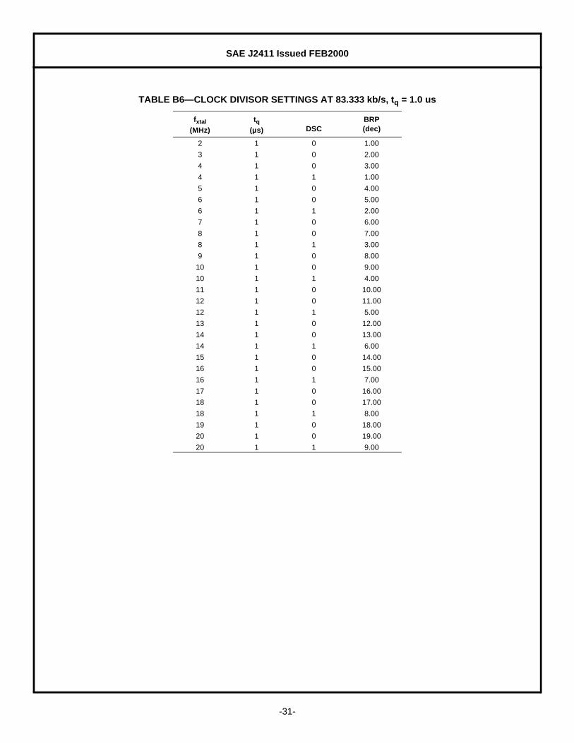
Table B4 defines compliant bit timing settings for operation at 83.333 kb/s.
Several acceptable example clock frequencies with their associated calculated CAN baud rate settings areshown in Table B5. Other sets may be possible with careful analysis.
TABLE B3—CLOCK DIVISOR SETTINGS AT 33.333 kb/s, tq = 2.0 us
Fxtal
(MHz)tq
(us) DSCBRP(dec)
2 2 0 3.00
2 2 1 1.00
3 2 0 5.00
3 2 1 2.00
4 2 0 7.00
4 2 1 3.00
5 2 0 9.00
5 2 1 4.00
6 2 0 11.00
6 2 1 5.00
8 2 0 15.00
8 2 1 7.00
10 2 0 19.00
10 2 1 9.00
12 2 0 23.00
12 2 1 11.00
15 2 0 29.00
15 2 1 14.00
16 2 0 31.00
16 2 1 15.00
20 2 0 39.00
20 2 1 19.00
TABLE B4—BIT SETTINGS AT 83.333 kb/s
tq tSJW tSEG2min tSEG2max TSEG1 TSEG2
0.6 µs 1.8 µs 1.8 µs 1.8 µs 15 2
1.0 µs 2.0 µs 2.0 µs 2.0 µs 8 1
TABLE B5—CLOCK DIVISOR SETTINGS AT 83.333 kb/s, tq = 0.6 us
fxtal(MHz)
tq(µs) DSC
BRP(dec)
5 0.6 0 2.00
10 0.6 0 5.00
10 0.6 1 2.00
15 0.6 0 8.00
20 0.6 0 11.00
20 0.6 1 5.00
25 0.6 0 14.00
SAE J2411 Issued FEB2000
-31-
TABLE B6—CLOCK DIVISOR SETTINGS AT 83.333 kb/s, tq = 1.0 us
fxtal
(MHz)tq
(µs) DSCBRP(dec)
2 1 0 1.00
3 1 0 2.00
4 1 0 3.00
4 1 1 1.00
5 1 0 4.00
6 1 0 5.00
6 1 1 2.00
7 1 0 6.00
8 1 0 7.00
8 1 1 3.00
9 1 0 8.00
10 1 0 9.00
10 1 1 4.00
11 1 0 10.00
12 1 0 11.00
12 1 1 5.00
13 1 0 12.00
14 1 0 13.00
14 1 1 6.00
15 1 0 14.00
16 1 0 15.00
16 1 1 7.00
17 1 0 16.00
18 1 0 17.00
18 1 1 8.00
19 1 0 18.00
20 1 0 19.00
20 1 1 9.00

SAE J2411 Issued FEB2000
-32-
APPENDIX C
NESTED SWC AND DWC IC PC BOARD LAYOUT
C.1 This shows an example printed circuit board layout which will allow either a single wire or a dual wire CANintegrated circuit to be installed in an ECU while minimizing the board space. The CAN controller must makeappropriate changes to accommodate CAN speed and control signals to the installed transceiver.See transceiver supplier specifications for the actual mounting and heat sinking requirements to maintainoperation over the entire specified operating temperature and voltage ranges.
FIGURE C1—SINGLE WIRE CAN AND DUAL WIRE CAN IC NESTED PC BOARD LAYOUT

SAE J2411 Issued FEB2000
Rationale—Not applicable.
Relationship of SAE Standard to ISO Standard—Not applicable.
Application—This SAE Recommended Practice defines the Physical Layer and portions of the Data LinkLayer of the OSI model for data communications. In particular, this document specifies the physicallayer requirements for any Carrier Sense Multiple Access/Collision Resolution (CSMA/CR) data linkwhich operates on a single wire medium to communicate among Electronic Control Units (ECU) on roadvehicles.
Requirements stated in this document will provide a minimum standard level of performance to which allcompatible ECUs and media shall be designed. This will assure full serial data communication amongall connected devices regardless of supplier.
This document is to be referenced by the particular vehicle OEM Component Technical Specificationwhich describes any given ECU in which the single wire data link controller and physical layer interfaceis located. Primarily, the performance of the physical layer is specified in this document. ECUenvironmental and other requirements when provided in the Component Technical Specification, shallsupercede the requirements of this document.
The intended audience includes, but is not limited to, ECU suppliers, CAN controller suppliers, CANtransceiver suppliers, component release engineers, and vehicle system engineers.
Reference Section
SAE J551—All parts—Performance Levels and Methods of Measurement of Electromagnetic Compatibilityfor Vehicles and Devices
SAE J1113—All parts—Electromagnetic Compatibility Measurement Procedures for Vehicle Components
SAE J1213-1—Glossary of Vehicle Networks for Multiplexing and Data Communications
SAE J1930—Electrical/Electronic Systems Diagnostic Terms, Definitions, Abbreviations and Acronyms
SAE J2284—High Speed CAN (HSC) for Vehicle Applications at 500 KBPS
ISO 7498—Data processing systems—Open systems interconnection standard reference mode
ISO 7637—Road vehicles—Electrical interference by conduction and coupling—Parts 1 and 2
Delphi - Delco Electronics Automotive Systems - DK166153 - Single Wire CAN Transceiver
Philips - AU5790 - Single Wire CAN Transceiver
Infineon - TLE 6255 - Single Wire CAN Transceiver
Bosch Controller Area Network 2.0 specification
CISPR 25 - Limits & Methods of Measurement of Radio Disturbance Characteristics for the Protection ofReceivers used on board vehicles.
Developed by the SAE Single Wire CAN Task Force
Sponsored by the SAE Vehicle Network for Multiplex and Data Communication Standards Committee

![Inhaltsverzeichnis · [ I ] SAE-Flansche (ISO 6162) / SAE-flanges (ISO 6162) Seite / Page SAE-Flanschhälften / SAE-split flange halves FH-... 1 SAE-Vollflansch / SAE-flange](https://img.pdfslide.net/doc/110x75/5b1675127f8b9a546d8c0fe1/inhaltsverzeichnis-i-sae-flansche-iso-6162-sae-flanges-iso-6162-seite.jpg)