Embed Size (px)
Citation preview
Slide 1 © 2015 Bhanushali & Davis
FreePDK15An Open-Source Predictive Process
Design Kit for 15nm FinFET Technology
Kirti Bhanushali, W. Rhett Davis (NCSU)
International Symposium on Physical Design
April 1, 2015
NC STATE UNIVERSITY
Slide 2 © 2015 Bhanushali & Davis
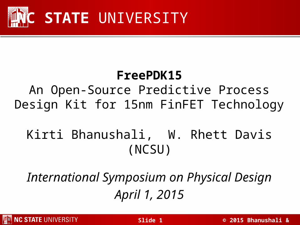
Motivation
Problem» Restrictions on PDKs prevent sharing of design data,
impede research & teaching
Solution» Free Predictive PDK, establishes a baseline for
research & teaching in design, architecture, manufacturing, and automation
FreePDK45 accomplished this for 45nm, FreePDK15 seeks to do the same for 15nm
Slide 3 © 2015 Bhanushali & Davis
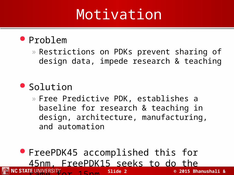
Process Cross Section
What everyone should know: FinFETs & MOL layers Thanks to Alex Toniolo (NanGate) for suggesting layers Schuddinck, et al (IEDM 2012) suggested dimensions
Si
FinsGate
AIL1
• Active Interconnect Level-1 (AIL1)
AIL1
AIL2 AIL2
• Active Interconnect Level-2 (AIL2)
GIL
• Gate Interconnect Layer (GIL)
• Layer Interconnect Overlap Level
Metal-1
• Level-2 Contact to Metal-1• (Applies to AIL-2 and GIL)
• FEOL
• BEOL
Slide 4 © 2015 Bhanushali & Davis
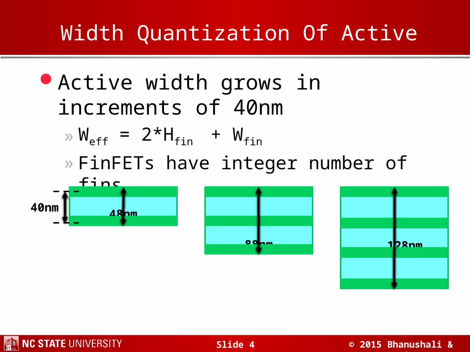
Width Quantization Of Active
Active width grows in increments of 40nm» Weff = 2*Hfin + Wfin
» FinFETs have integer number of fins
48nm •
88nm 128nm
40nm
Slide 5 © 2015 Bhanushali & Davis
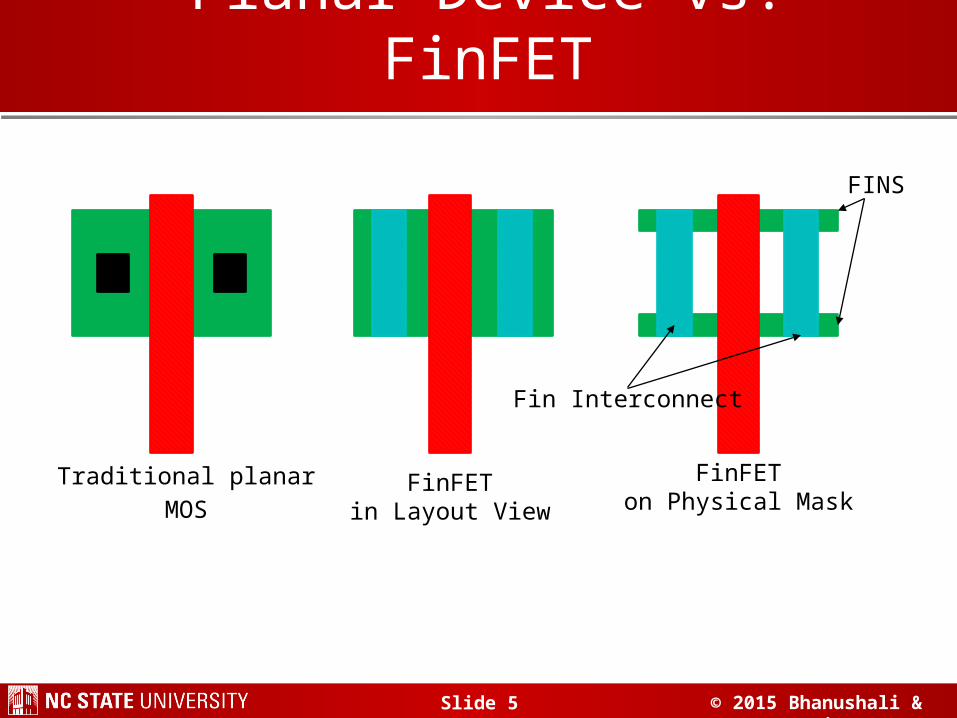
Planar Device vs. FinFET
• Traditional planar• MOS
FinFETin Layout View
FinFETon Physical Mask
• FINS
• Fin Interconnect
Slide 6 © 2015 Bhanushali & Davis
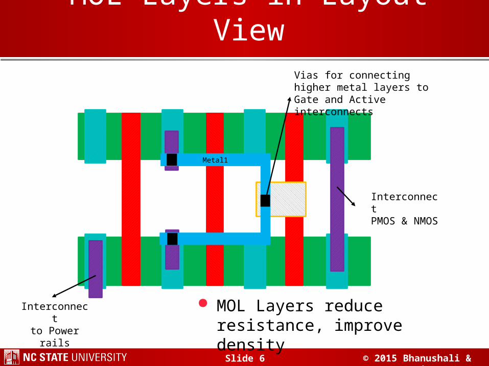
MOL Layers in Layout View
MOL Layers reduce resistance, improve density
Metal1
Interconnectto Power rails
• InterconnectPMOS & NMOS
Vias for connecting higher metal layers to Gate and Active interconnects
Slide 7 © 2015 Bhanushali & Davis
Met
al1A
Met
al1B
Met
al1A
Met
al1A
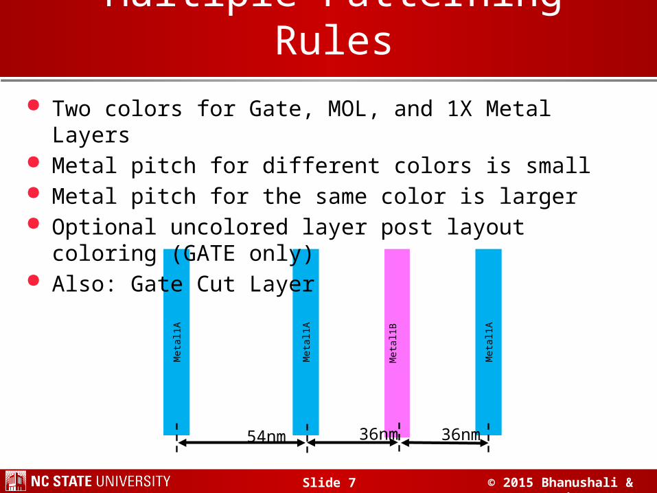
• 36nm • 36nm• 54nm
Multiple-Patterning Rules
Two colors for Gate, MOL, and 1X Metal Layers Metal pitch for different colors is small Metal pitch for the same color is larger Optional uncolored layer post layout coloring (GATE only) Also: Gate Cut Layer
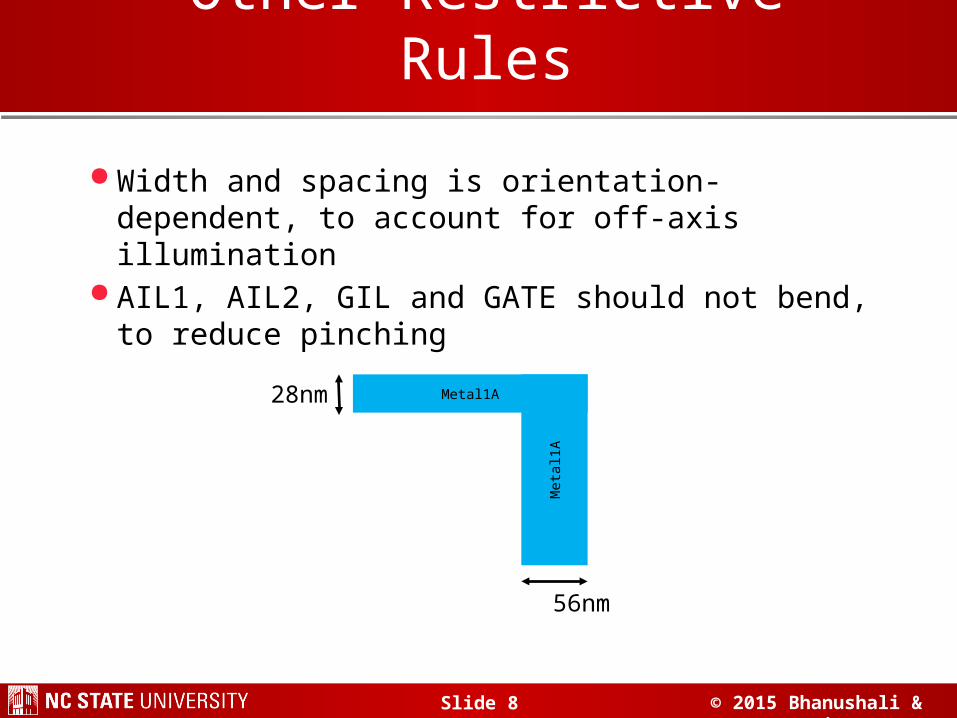
Slide 8 © 2015 Bhanushali & Davis
Other Restrictive Rules
Width and spacing is orientation-dependent, to account for off-axis illumination
AIL1, AIL2, GIL and GATE should not bend, to reduce pinching
Met
al1A
Metal1A• 28nm
• 56nm
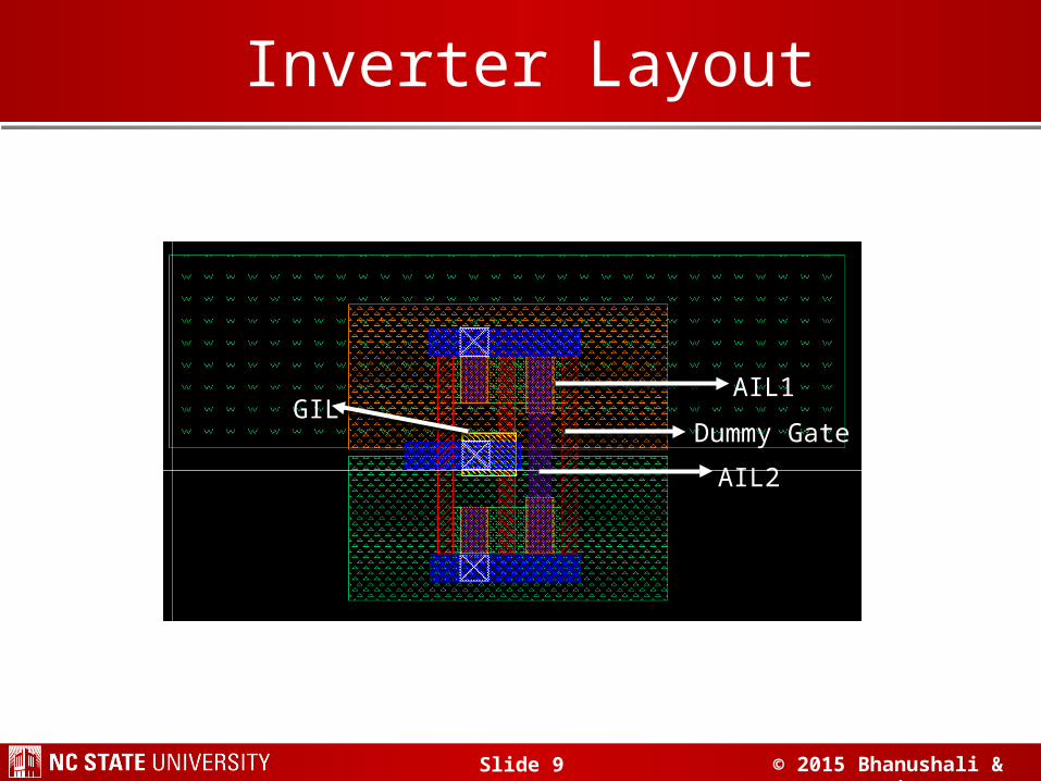
Slide 9 © 2015 Bhanushali & Davis
Layout – Inverter
Dummy Gate
AIL1
AIL2
GIL
Inverter Layout
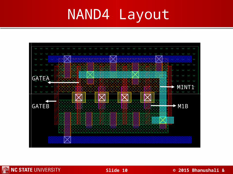
Slide 10 © 2015 Bhanushali & Davis
NAND4
MINT1
M1B
GATEA
GATEB
NAND4 Layout
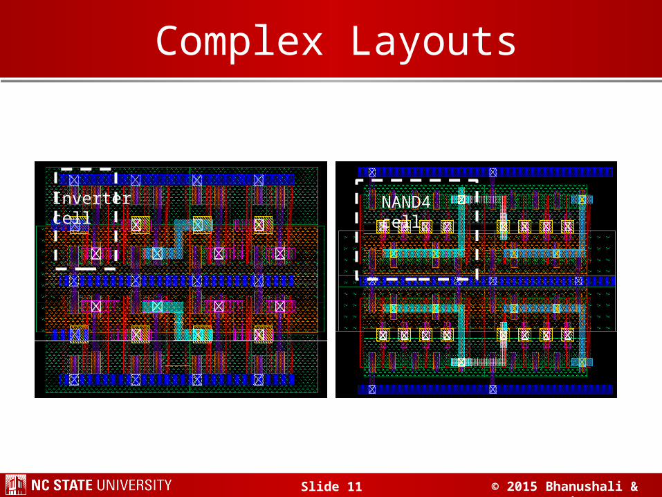
Slide 11 © 2015 Bhanushali & Davis
Complex Layouts
Inverter cell NAND4 cell
Complex Layouts
Slide 12 © 2015 Bhanushali & Davis
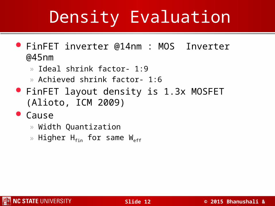
Layout Density Comparison FinFET inverter @14nm : MOS Inverter @45nm
» Ideal shrink factor- 1:9» Achieved shrink factor- 1:6
FinFET layout density is 1.3x MOSFET (Alioto, ICM 2009)
Cause» Width Quantization
» Higher Hfin for same Weff
Density Evaluation
Slide 13 © 2015 Bhanushali & Davis
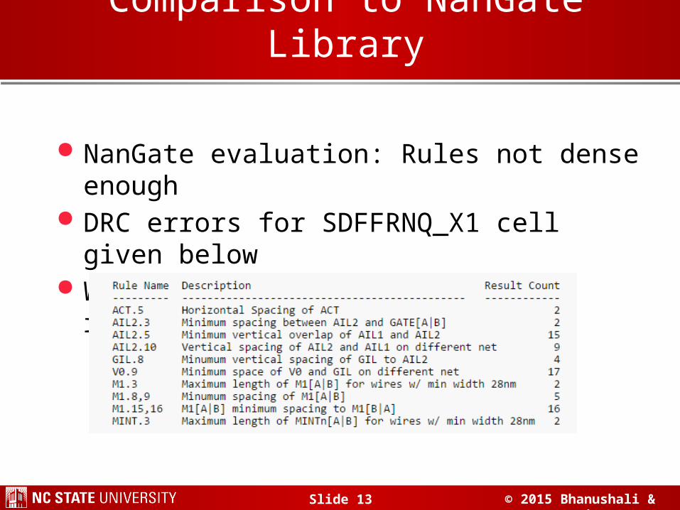
Comparison to NanGate Library
NanGate evaluation: Rules not dense enough DRC errors for SDFFRNQ_X1 cell given below Working with NanGate to revise rules
Slide 14 © 2015 Bhanushali & Davis
Future Releases
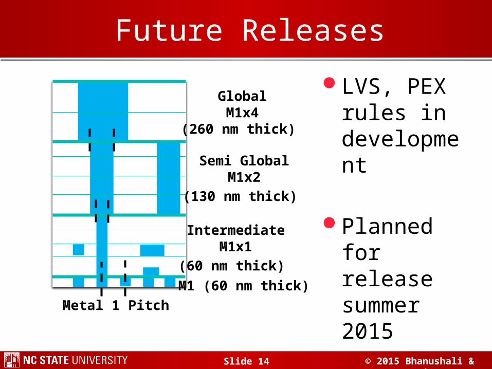
LVS, PEX rules in development
Planned for release summer 2015
Semi GlobalM1x2
(130 nm thick)
IntermediateM1x1
(60 nm thick)
M1 (60 nm thick)
GlobalM1x4
(260 nm thick)
Metal 1 Pitch
Slide 15 © 2015 Bhanushali & Davis
Licensing
Licensed for Academic Use under 3-clause BSD License» Caveat: Cannot distribute a Cell Library until
Summer 2016
Please contact us for commercial license» Click through license may be possible with
your help
Slide 16 © 2015 Bhanushali & Davis
Conclusion
First-pass FreePDK15 with DRC is now available, including new 15nm features» FinFETs» MOL Layers» Multiple Patterning
LVS & PEX rules available in summer How you can help» Feedback on design rules» Request a commercial use license
Slide 17 © 2015 Bhanushali & Davis
Acknowledgement Alex Toniolo Joseph Davis, Tarek Ramadan, Ahmed
Hammed Fathy, Omar El-Sewefy , Ahmed El-Kordy, Hend Wagieh (Mentor Graphics)
Acknowledgements