Embed Size (px)
Citation preview

Slide 1
V. Paidi, Z. Griffith, Y. Wei, M. Dahlstrom,
N. Parthasarathy, M. Seo, M. Urteaga,
M. J. W. Rodwell ,Department of Electrical and Computer Engineering,
University of California, Santa Barbara, CA 93106
L. Samoska, A. Fung,Jet Propulsion Labs, Pasadena, CA 91109
Common Base Amplifier with 7- dB gain at 176 GHz in
InP mesa DHBT Technology

Slide 2
Outline
• Motivation.
• Why Common-base?
• Effect of layout parasitics on circuit stability and MSG.
• InP mesa DHBT process.
• Circuit simulations.
• Device Results
• G-band Power amplifier results.
• W-band Power amplifier results.

Slide 3
Motivation and Previous Results
• Applications for electronics in 140-220 GHz frequency band
Wideband communication systems Atmospheric sensing Automotive radar
• Small signal amplifier results
6.3 dB @ 175 GHz single stage amplifier in InP TSHBT technology, Miguel et.al.,12 dB @ 170 GHz three stage CE amplifier in InP TSHBT technology, Miguel et. al., 6-stage amplifier with 20 6 dB from 150-215 GHz, InP HEMT, Weinreb et. al.
• Power amplifier results 14-16 dBm @140-170 GHz with 10 dB gain in InP HEMT technology, Lorene et. al., 12.5 dBm @90 GHz with 8.6 dB gain in TS InP DHBT technology, Yun et. al., 14-16 dBm @65-145 GHz with > 10 dB gain in InP HEMT technology, Lorene et. al.,

Slide 4
Why mesa -InP HBTs for 140- 220 GHz power amplifiers ?
• fmax > 400 GHz, ft > 250 GHz
• High current density > 3 mA/ m2.
• Vbr,ce0 > 6V
• Low thermal resistance.
High power density, high gain in 140-220-GHz frequency range

Slide 5
Why Common Base ?
RL
InputMatchingnetworkVin Vout
OutputLoadlineMatchingnetwork
Common Base Circuit Schematic
0
5
10
15
20
25
30
10 100
MS
G/M
AG
, dB
Frequency, GHz
Common base
Common Collector
Common emitter
U
Common base has the highest MSG/MAG.

Slide 6
Base inductance
• 0.8 m base contact width Leads to base access inductance.
• Lb ~ 3 pH for 0.8 mX12 m HBT.
Longer finger length results in larger base access inductance
emitter
Ground
Emitter access
Interconnect metal
Polyimidebase
0.8m each
Slide 7
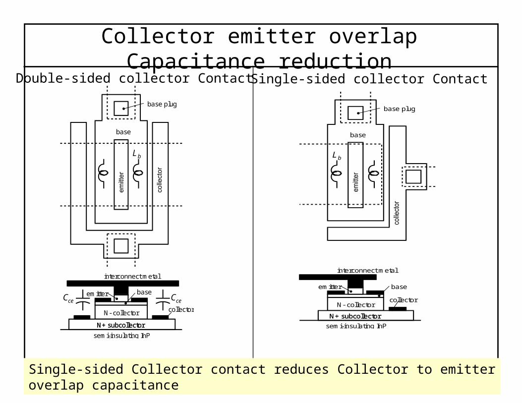
Collector emitter overlap Capacitance reduction
base plug
emitter
semi-insulating InP
N+ subcollector
N- collector
base
collector
N+ subcollector
Lb
CceCce
base
interconnect metal
base plug
emitter
semi-insulating InP
N+ subcollector
N- collector
base
collector
N+ subcollector
Lb
base
interconnect metal
Double-sided collector Contact Single-sided collector Contact
Single-sided Collector contact reduces Collector to emitter overlap capacitance

Slide 8
Cce, Lb degrade MSG/MAG
0
5
10
15
20
25
10 100
MS
G/M
AG
Frequency, GHz
Without Cce
, Lb
With Cce
With Cce
, Lb
base plug
emitter
semi-insulating InP
N+ subcollector
N- collector
base
collector
N+ subcollector
Lb
CceCce
base
interconnect metal
Lb reduces MSG in 140-220-GHz frequency range.

Slide 9
Single-sided collector Contact improves MSG
0
5
10
15
20
25
30
10 100
MS
G/M
AG
Frequency, GHz
Single sided collector
Double sided collector
amplifier designs
base plug
emitter
semi-insulating InP
N+ subcollector
N- collector
base
collector
N+ subcollector
Lb
base
interconnect metal
2-3-dB improvement in MSG.

Slide 10
• Both junctions defined by selective wet-etch chemistry
• Low contact resistances
• NiCr thin film resistors s = 40 /
• MIM capacitor, SiN dielectric.
• ADS momentum modeled CPW transmission lines
• Air bridges strap ground planes
Mesa IC Process: overview
SI InP
CollectorBaseE
sub-collector
polymide NiCr metal 1 SiN Air bridge

Slide 11
Single-stage Common Base power amplifier
Circuit Schematic
Objectives: 180 GHz amplifier, Psat~ 20 dBm
Approach: InP mesa-DHBTs
Simulations: ADS S-parameter, harmonic balance and momentum simulations
RLVoutVin
Input matching network Output loadlinematch
Input matching network Output loadlinematch

Slide 12
Output Large-signal Load-line match
Rex
Ccb
C
Rcb
Rb,spread
Rb,gap
Rb,cont
Lb
Cgap
Cccbx(1-F)
Cccbx(F)
CceRc,spread /2
Rc,spread /2
Rc,cont
Base
Emitter
Collector
A
v
Device Model Load-line match
Circuit optimized for output power not gain
(Simulations)

Slide 13
Single-stage Common Base power amplifier
2 x 2 x 0.8 m x 12 m, AE=38 m2
(Simulations)
-10
-5
0
5
10
100 125 150 175 200 225 250
S2
1, S
11,
S2
2 d
B
frequency, GHz
S21
S22
S11
0
5
10
15
20
0
5
10
15
20
0 5 10 15 20
Out
put P
ow
er,
dB
m, G
ain
, dB
PA
E (%
)
Input Power, dBm
Pout
PAE
Gain
5.3 dB at 180 GHz, 3-dB Bandwidth = 45 GHz, Saturated Pout, = 20 dBm
• Frequency of operation =180 GHz
• 3-dB bandwidth = 45 GHz,
• Gain = 5.3 dB at 180 GHz,
• Pout,sat = 20 dBm.

Slide 14
Two-stage Common Base amplifier
RLVoutVin
50 Ohms 50 Ohms
InputMatchingNetwork
OutputLoadlineMatchingNetwork
InputMatchingNetwork
OutputLoadlineMatchingNetwork
at f0
at f0
Veb,bias
Vcb,bias
Circuit Schematic
Objectives: 180 GHz amplifier, Psat~ 20 dBm
Approach: InP mesa-DHBTs
Simulations: S-parameter and harmonic and momentum simulation in ADS

Slide 15
Two-stage Common Base amplifier
-10
-5
0
5
10
15
150 160 170 180 190 200 210 220
S2
1,
S1
1,
S2
2 d
B
frequency, GHz
S21
S11
S22
6 x 0.8m x 12 m, AE=58 m2
0
5
10
15
20
0 2 4 6 8 10 12 14
Outp
ut P
ow
er,
dB
m,
Ga
in,
dB
Input Power, dBm
Pout
Gain
Frequency of operation =180 GHz
3-dB bandwidth = 45 GHz,
Gain = 8.7 dB,
Pout,sat = 19.5 dBm.
(Simulations)
Power simulations at 180 GHz
Slide 16
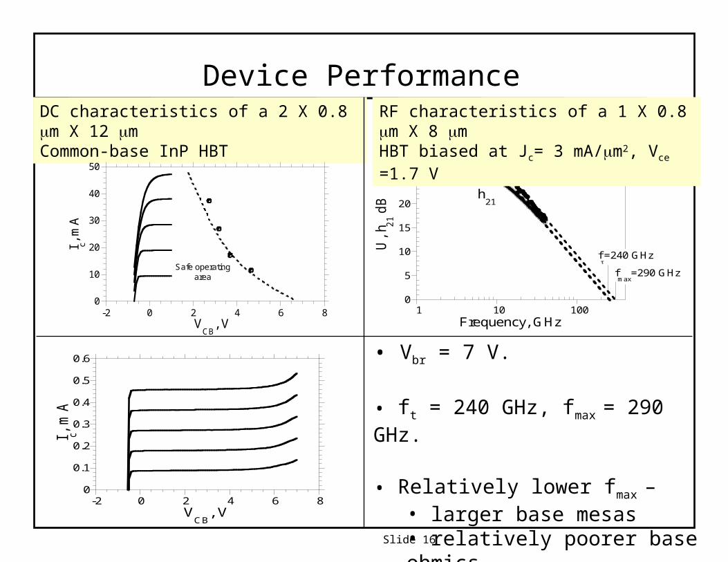
Device Performance DC characteristics of a 2 X 0.8 m X 12 m Common-base InP HBT
0
10
20
30
40
50
-2 0 2 4 6 8
I c, mA
VCB
, V
Safe operatingarea
0
0.1
0.2
0.3
0.4
0.5
0.6
-2 0 2 4 6 8
I c, m
A
VCB
, V
0
5
10
15
20
25
30
1 10 100
U, h 2
1 dB
Frequency, GHz
U
h21
f=240 GHz
fmax
=290 GHz
RF characteristics of a 1 X 0.8 m X 8 m HBT biased at Jc= 3 mA/m2, Vce =1.7 V
• Vbr = 7 V.
• ft = 240 GHz, fmax = 290 GHz.
• Relatively lower fmax –• larger base mesas • relatively poorer base ohmics.

Slide 17
Power measurement setup 170-180 GHz
Power meter
Frequencydoubler
W-band PA
DUT
BWOPowerSource
Variableattenuator
W-bandPoweramplifier
W-bandPowermeter
SchottkyDoubler
WR-5Picoprobe
Calorimeter
Probe loss 170-180 GHz band ~ 2.6 dBWR-5Picoprobe
DUT

Slide 18
Power measurement setup 150 GHz
150 GHzGunnPowerSource Variable
attenuator
WR-5Wafer Probe
Calorimeter
Probe loss 150 GHz band ~ 3.0 dB
WR-5Wafer Probe
DUT
Gunn Oscillator
Var Attn
DUT
Calorimeter
Slide 19
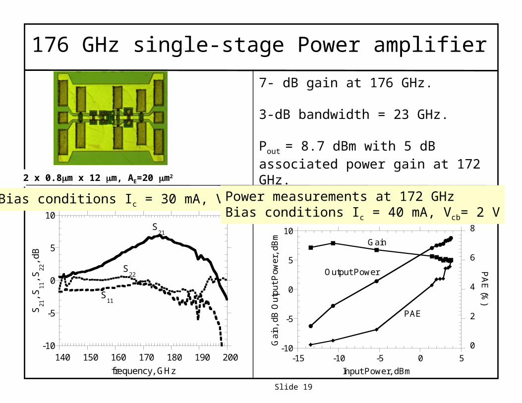
176 GHz single-stage Power amplifier
2 x 0.8m x 12 m, AE=20 m2
7- dB gain at 176 GHz.
3-dB bandwidth = 23 GHz.
Pout = 8.7 dBm with 5 dB associated power gain at 172 GHz.
-10
-5
0
5
10
140 150 160 170 180 190 200
S2
1, S
11,
S2
2, dB
frequency, GHz
S21
S22
S11
-10
-5
0
5
10
0
2
4
6
8
-15 -10 -5 0 5
Gai
n,
dB O
utp
ut P
ower
, dB
m
PA
E (%
)
Input Power, dBm
Gain
Output Power
PAE
Bias conditions Ic = 30 mA, Vcb= 1 V Power measurements at 172 GHzBias conditions Ic = 40 mA, Vcb= 2 V

Slide 20
176 GHz single-stage Power amplifier
At 172 GHz 7.53 mW output power with 5 dB associated gain.
Maximum power measured = 8.37 mW at 176 GHz
0
2
4
6
8
10
170 171 172 173 174 175 176 177
Max
imum
Out
put
Pow
er,
dBm
Frequency, GHz
Associated power gain
Maximum output power
Slide 21
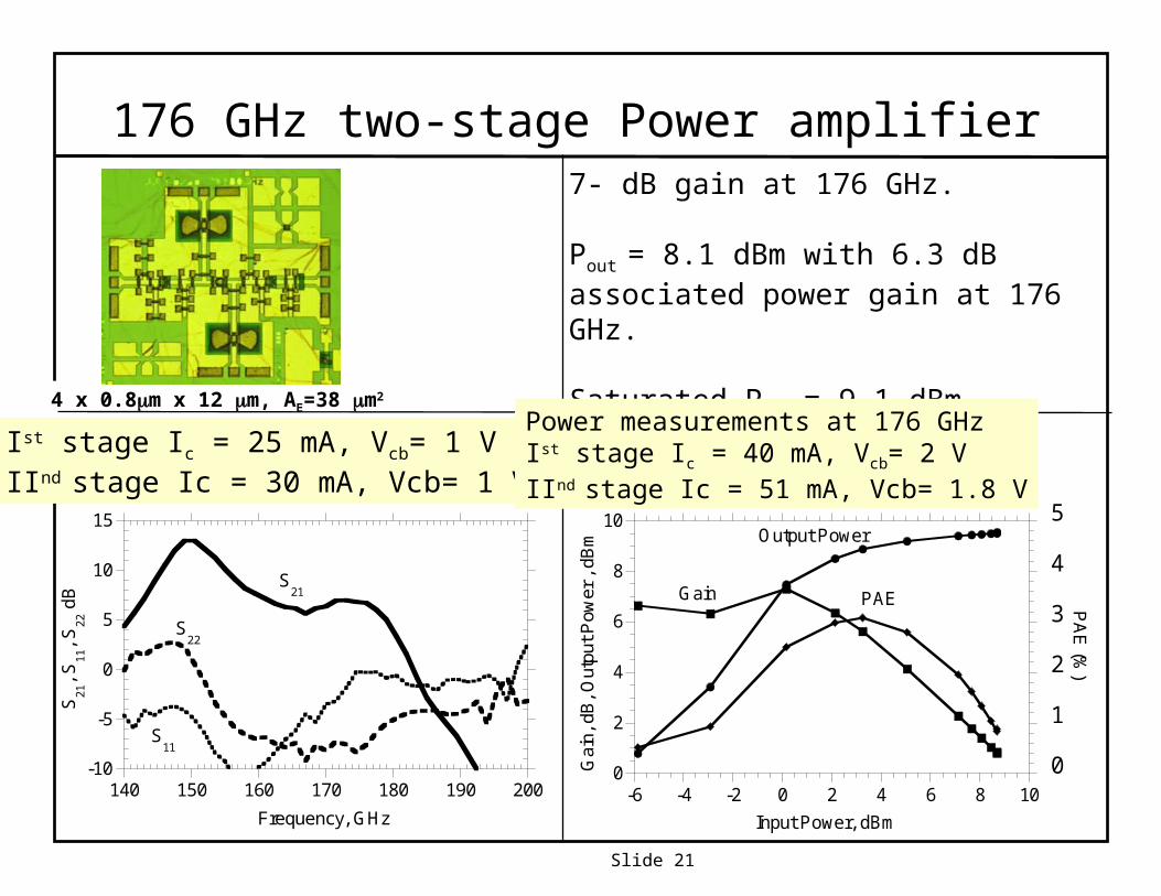
176 GHz two-stage Power amplifier
4 x 0.8m x 12 m, AE=38 m2
7- dB gain at 176 GHz.
Pout = 8.1 dBm with 6.3 dB associated power gain at 176 GHz.
Saturated Pout = 9.1 dBm
Ist stage Ic = 25 mA, Vcb= 1 VIInd stage Ic = 30 mA, Vcb= 1 V
0
2
4
6
8
10
0
1
2
3
4
5
-6 -4 -2 0 2 4 6 8 10
Gai
n, d
B, O
utpu
t Pow
er ,
dBm
PA
E (%
)
Input Power, dBm
PAEGain
Output Power
-10
-5
0
5
10
15
140 150 160 170 180 190 200
S2
1,
S1
1,
S2
2 d
B
Frequency, GHz
S21
S11
S22
Power measurements at 176 GHzIst stage Ic = 40 mA, Vcb= 2 VIInd stage Ic = 51 mA, Vcb= 1.8 V

Slide 22
176 GHz two-stage Power amplifier
At 150.2 GHz 10.3 dBm Pout with 3.4 dB associated gain.
-5
0
5
10
15
0
2
4
6
-10 -5 0 5 10
Gai
n, d
B,
Out
put
Pow
er, d
Bm
PA
E (%
)
Input Power, dBm
Gain Output Power
PAE

Slide 23
84 GHz single-stage Power amplifier
4 x 0.8m x 12 m, AE=38 m2
6.5- dB gain at 84 GHz.
Pout = 32.4 mW with 4 dB associated power gain at 84 GHz.
Bias conditions Ic = 37 mA, Vcb= 1 V Power measurements at 84 GHzBias conditions Ic = 56 mA, Vcb= 2.2 V
-10
-5
0
5
10
75 80 85 90 95 100 105 110
S21
, S
11,
S22
, dB
Frequency, GHz
S21
S22
S11
4
6
8
10
12
14
16
0
5
10
15
20
0 2 4 6 8 10 12
Gai
n, d
B,
Out
put
Pow
er, d
Bm
PA
E (%
)
Input Power, dBm
Pout
PAE
Gain
Slide 24
Design and fabrication of W-band (75-110-GHz) G – band (140-220-GHz) power amplifiers in InP mesa DHBT technology
7-dB at 176 GHz with a single-stage common-base amplifier.
Obtained 8.77dBm output power with 5-dB associated power gain at 172 GHz.
Obtained 32 mW at 84 GHz.
Accomplishments
This work was supported by the ONR , JPL , DARPA (USA).