Embed Size (px)
Citation preview

1. Introduction
This document describes the functionality and electrical specifications of the contactless reader/writer IC SLRC610.
2. General description
The SLRC610 is a highly integrated transceiver IC for contactless communication at 13.56 MHz.
The SLRC610 transceiver IC supports the following operating modes
• Read/write mode supporting ISO/IEC 15693
• Read/write mode supporting ICODE EPC UID/ EPC OTP
• Read/write mode supporting ISO/IEC 18000-3 mode 3/ EPC Class-1 HF
The SLRC610 supports the vicinity protocol according to ISO/IEC15693, EPC UID and ISO/IEC 18000-3 mode 3/ EPC Class-1 HF.
The following host interfaces are supported:
• Serial Peripheral Interface (SPI)
• Serial UART (similar to RS232 with voltage levels dependent on pin voltage supply)
• I2C-bus interface (two versions are implemented: I2C and I2CL)
The SLRC610 supports the connection of a secure access module (SAM). A dedicated separate I2C interface is implemented for a connection of the SAM. The SAM can be used for high secure key storage and acts as a very performant crypto coprocessor. A dedicated SAM is available for connection to the SLRC610.
3. Features and benefits
High RF output power frontend IC
Supports ISO/IEC15693, ICODE EPC UID and ISO/IEC 18000-3 mode 3/ EPC Class-1 HF
Low-Power Card Detection
Antenna connection with minimum number of external components
Supported host interfaces:
SPI up to 10 Mbit/s
I2C-bus interfaces up to 400 kBd in Fast mode, up to 1000 kBd in Fast mode plus
SLRC610High performance ISO/IEC 15693 reader solutionRev. 3.4 — 6 February 2014227634
Product data sheetCOMPANY PUBLIC

NXP Semiconductors SLRC610High performance ISO/IEC 15693 reader solution
RS232 Serial UART up to 1228.8 kBd, with voltage levels dependent on pin voltage supply
Separate I2C-bus interface for connection of a secure access module (SAM)
FIFO buffer with size of 512 byte for highest transaction performance
Flexible and efficient power saving modes including hard power down, standby and low-power card detection
Cost saving by integrated PLL to derive system CPU clock from 27.12 MHz RF quartz crystal
3 V to 5.5 V power supply
Up to 8 free programmable input/output pins
4. Quick reference data
[1] VDD(PVDD) must always be the same or lower voltage than VDD.
[2] Ipd is the sum of all supply currents
[3] IDD(TVDD) depends on VDD(TVDD) and the external circuitry connected to TX1 and TX2.
[4] Typical value: Assumes the usage of a complementary driver configuration and an antenna matched to 40 between pins TX1, TX2 at 13.56 MHz.
5. Ordering information
[1] Delivered in one tray
[2] Delivered in five trays
[3] Delivered on reel with 6000 pieces
Table 1. Quick reference data
Symbol Parameter Conditions Min Typ Max Unit
VDD supply voltage 3 5 5.5 V
VDD(PVDD) PVDD supply voltage [1] 3 5 VDD V
VDD(TVDD) TVDD supply voltage 3 5 5.5 V
Ipd power-down current PDOWN pin pulled HIGH [2] - 8 40 nA
IDD supply current - 17 20 mA
IDD(TVDD) TVDD supply current [3][4] - 100 200 mA
Tamb ambient temperature 25 +25 +85 C
Tstg storage temperature no supply voltage applied 40 +25 +100 C
Table 2. Ordering information
Type number Package
Name Description Version
SLRC61002HN/TRAYB[1] HVQFN32 plastic thermal enhanced very thin quad flat package; no leads; MSL1, 32 terminals + 1 central ground; body 5 5 0.85 mm
SOT617-1
SLRC61002HN/TRAYBM[2]
SLRC61002HN/T/R[3]
SLRC610 All information provided in this document is subject to legal disclaimers. © NXP B.V. 2014. All rights reserved.
Product data sheetCOMPANY PUBLIC
Rev. 3.4 — 6 February 2014227634 2 of 117
NXP Semiconductors SLRC610High performance ISO/IEC 15693 reader solution
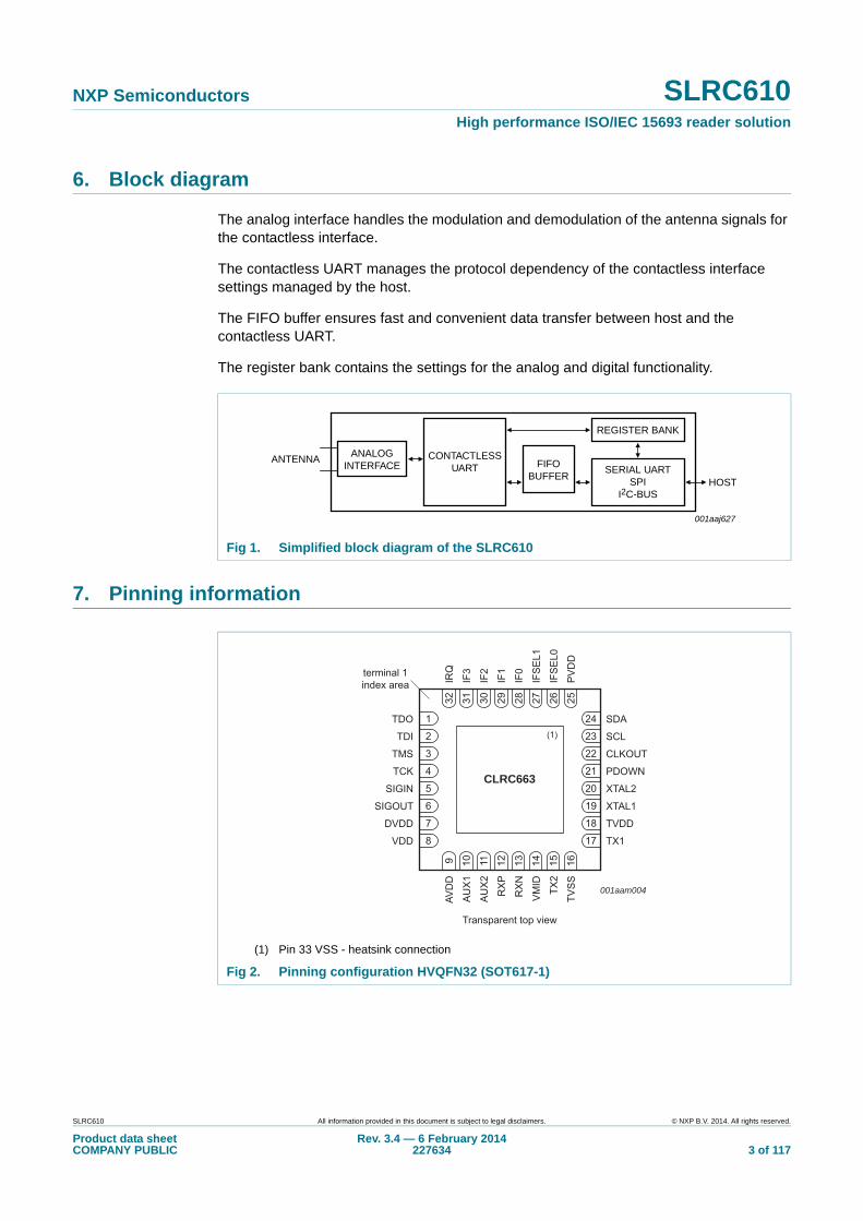
6. Block diagram
The analog interface handles the modulation and demodulation of the antenna signals for the contactless interface.
The contactless UART manages the protocol dependency of the contactless interface settings managed by the host.
The FIFO buffer ensures fast and convenient data transfer between host and the contactless UART.
The register bank contains the settings for the analog and digital functionality.
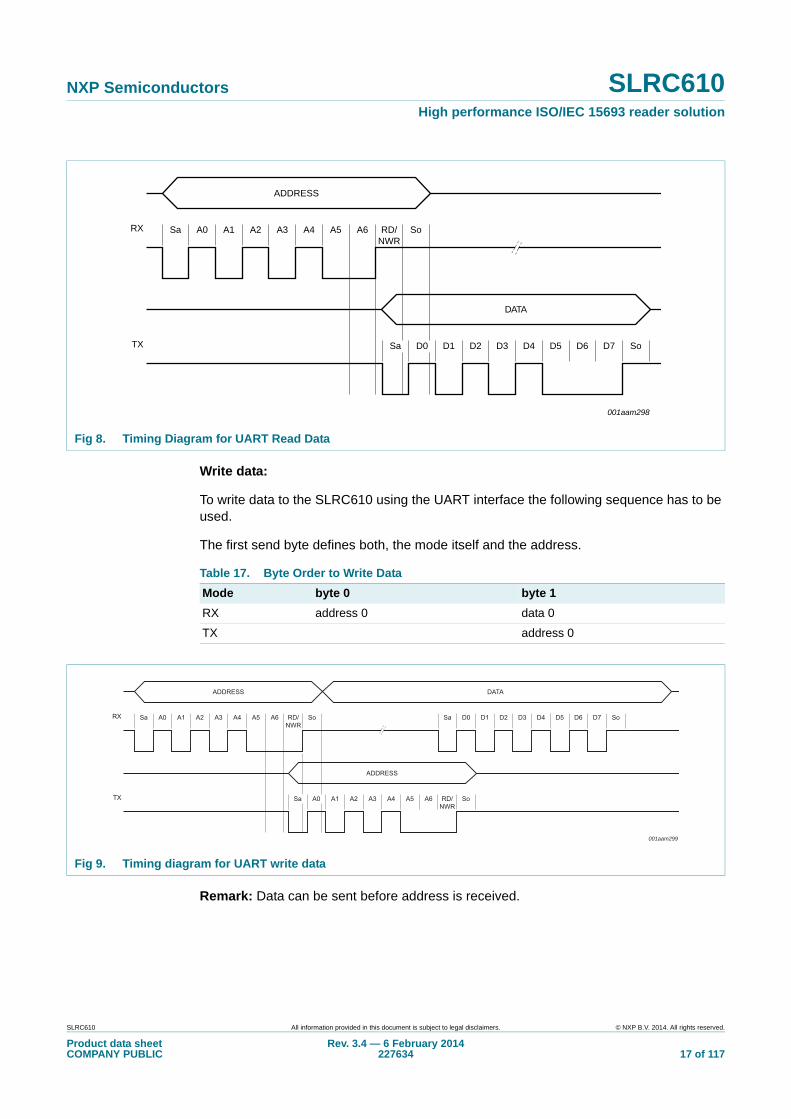
7. Pinning information
Fig 1. Simplified block diagram of the SLRC610
001aaj627
HOST
ANTENNA FIFOBUFFER
ANALOGINTERFACE
CONTACTLESSUART SERIAL UART
SPII2C-BUS
REGISTER BANK
(1) Pin 33 VSS - heatsink connection
Fig 2. Pinning configuration HVQFN32 (SOT617-1)
001aam004
CLRC663
Transparent top view
TX1
(1)
DVDD
VDD
TVDD
SIGOUT XTAL1
SIGIN XTAL2
TCK PDOWN
TMS CLKOUT
TDI SCL
TDO SDA
AVD
D
AU
X1
AU
X2
RX
P
RX
N
VM
ID
TX2
TVS
S
IRQ
IF3
IF2
IF1
IF0
IFS
EL1
IFS
EL0
PV
DD
8 17
7 18
6 19
5 20
4 21
3 22
2 23
1 24
9 10 11 12 13 14 15 16
32 31 30 29 28 27 26 25
terminal 1index area
SLRC610 All information provided in this document is subject to legal disclaimers. © NXP B.V. 2014. All rights reserved.
Product data sheetCOMPANY PUBLIC
Rev. 3.4 — 6 February 2014227634 3 of 117

NXP Semiconductors SLRC610High performance ISO/IEC 15693 reader solution
7.1 Pin description
[1] This pin is used for connection of a buffer capacitor. Connection of a supply voltage might damage the device.
Table 3. Pin description
Pin Symbol Type Description
1 TDO O test data output for boundary scan interface
2 TDI I test data input boundary scan interface
3 TMS I test mode select boundary scan interface
4 TCK I test clock boundary scan interface
5 SIGIN I Contactless communication interface output.
6 SIGOUT O Contactless communication interface input.
7 DVDD PWR digital power supply buffer [1]
8 VDD PWR power supply
9 AVDD PWR analog power supply buffer [1]
10 AUX1 O auxiliary outputs: Pin is used for analog test signal
11 AUX2 O auxiliary outputs: Pin is used for analog test signal
12 RXP I receiver input pin for the received RF signal.
13 RXN I receiver input pin for the received RF signal.
14 VMID PWR internal receiver reference voltage [1]
15 TX2 O transmitter 2: delivers the modulated 13.56 MHz carrier
16 TVSS PWR transmitter ground, supplies the output stage of TX1, TX2
17 TX1 O transmitter 1: delivers the modulated 13.56 MHz carrier
18 TVDD PWR transmitter voltage supply
19 XTAL1 I crystal oscillator input: Input to the inverting amplifier of the oscillator. This is pin is also the input for an externally generated clock (fosc = 27,12 MHz)
20 XTAL2 O crystal oscillator output: output of the inverting amplifier of the oscillator
21 PDOWN I Power Down
22 CLKOUT O clock output
23 SCL O Serial Clock line
24 SDA I/O Serial Data Line
25 PVDD PWR pad power supply
26 IFSEL0 I host interface selection 0
27 IFSEL1 I host interface selection 1
28 IF0 I/O interface pin, multifunction pin: Can be assigned to host interface RS232, SPI, I2C, I2C-L
29 IF1 I/O interface pin, multifunction pin: Can be assigned to host interface SPI, I2C, I2C-L
30 IF2 I/O interface pin, multifunction pin: Can be assigned to host interface RS232, SPI, I2C, I2C-L
31 IF3 I/O interface pin, multifunction pin: Can be assigned to host interface RS232, SPI, I2C, I2C-L
32 IRQ O interrupt request: output to signal an interrupt event
33 VSS PWR ground and heatsink connection
SLRC610 All information provided in this document is subject to legal disclaimers. © NXP B.V. 2014. All rights reserved.
Product data sheetCOMPANY PUBLIC
Rev. 3.4 — 6 February 2014227634 4 of 117

xxxxxxxxxxxxxxxxxxxxx xxxxxxxxxxxxxxxxxxxxxxxxxx xxxxxxx x x x xxxxxxxxxxxxxxxxxxxxxxxxxxxxxx xxxxxxxxxxxxxxxxxxx xx xx xxxxx xxxxxxxxxxxxxxxxxxxxxxxxxxx xxxxxxxxxxxxxxxxxxx xxxxxx xxxxxxxxxxxxxxxxxxxxxxxxxxxxxxxxxxx xxxxxxxxxxxx x x xxxxxxxxxxxxxxxxxxxxx xxxxxxxxxxxxxxxxxxxxxxxxxxxxxx xxxxx xxxxxxxxxxxxxxxxxxxxxxxxxxxxxxxxxxxxxxxxxxxxxxxxxx xxxxxxxx xxxxxxxxxxxxxxxxxxxxxxxxx xxxxxxxxxxxxxxxxxxxx xxx
SL
RC
610
Pro
du
ct data sh
CO
MP
AN
Y P
UB
L
NX
P S
emico
nd
ucto
rsS
LR
C610
Hig
h p
erform
an
ce
ISO
/IEC
15
693 rea
der s
olu
tion
8. Functional description
001aam005
PLLLFO
OSCTX
VOLTAGEREGULATOR
3/5 V =>1.8 VAVDD
RNG
UE FRONT-END
RESETLOGIC PDOWN
TX1TX2
XTAL1XTAL2
VDDVSSPVDDTVDDTVSS
AUX1AUX2
AVDDDVDD
CLKOUT
All inform
ation provided
in this docum
ent is subject to leg
al disclaim
ers.©
NX
P B
.V. 2014. A
ll rights reserved.
eetIC
Rev. 3.4 —
6 Feb
ruary 2014
227634 5 o
f 117
Fig 3. Detailed block diagram of the SLRC610
I2C,LOGICAL
FIFO512 Bytes
REGISTERS
STATEMACHINES
EEPROM8 kByte
SPI
SAM interface
VOLTAGEREGULATOR
3/5 V =>1.8 VDVDD
POR
ADC
RX
ANALOG
BOUNDARYSCAN
IF0
IFSEL0
IFSEL1
IF1
IF2
IF3
TCKTDI
TMSTDO
I2C
RS232
SPI
host interfaces
INTERRUPTCONTROLLER
IRQ SIGIN
TIMER0..3
CRC
TIMER4(WAKE-UP
TIMER)
SIGPRO
TXCODEC
RXDECOD
CL-COPROSIGIN/
SIGOUTCONTROL
SIGOUT VMID RXNRXP
SDASCL

NXP Semiconductors SLRC610High performance ISO/IEC 15693 reader solution
8.1 Interrupt controller
The interrupt controller handles the enabling/disabling of interrupt requests. All of the interrupts can be configured by firmware. Additionally, the firmware has possibilities to trigger interrupts or clear pending interrupt requests. Two 8-bit interrupt registers IRQ0 and IRQ1 are implemented, accompanied by two 8-bit interrupt enable registers IRQ0En and IRQ1En. A dedicated functionality of bit 7 to set and clear bits 0 to 6 in this interrupt controller registers is implemented.
The SLRC610 indicates certain events by setting bit IRQ in the register Status1Reg and additionally, if activated, by pin IRQ. The signal on pin IRQ may be used to interrupt the host using its interrupt handling capabilities. This allows the implementation of efficient host software.
The following table shows the available interrupt bits, the corresponding source and the condition for its activation. The interrupt bit TimernIrq in register IRQ1 indicates an interrupt set by the timer unit. The setting is done if the timer underflows.
The TxIrq bit in register IRq0 indicates that the transmission is finished. If the state changes from sending data to transmitting the end of the frame pattern, the transmitter unit sets the interrupt bit automatically.
The bit RxIrq in register IRQ0 indicates an interrupt when the end of the received data is detected.
The bit IdleIrq in register IRQ0 is set if a command finishes and the content of the command register changes to idle.
The waterlevel defines both - minimum and maximum warning levels - counting from top and from bottom of the FIFO by a single value.
The bit HiAlertIrq in register IRQ0 is set to logic 1 if the HiAlert bit is set to logic 1, that means the FIFO data number has reached the top level as configured by the bit WaterLevel.
The bit LoAlertIrq in register IRQ0 is set to logic 1 if the LoAlert bit is set to logic 1, that means the FIFO data number has reached the bottom level as configured by the bit WaterLevel.
The bit ErrIrq in register IRQ0 indicates an error detected by the contactless UART during receive. This is indicated by any bit set to logic 1 in register Error.
The bit LPCDIrq in register IRQ0 indicates a card detected.
The bit RxSOFIrq in register IRQ0 indicates a detection of a SOF or a subcarrier by the contactless UART during receiving.
The bit GlobalIRq in register IRQ1 indicates an interrupt occurring at any other interrupt source when enabled.
SLRC610 All information provided in this document is subject to legal disclaimers. © NXP B.V. 2014. All rights reserved.
Product data sheetCOMPANY PUBLIC
Rev. 3.4 — 6 February 2014227634 6 of 117

NXP Semiconductors SLRC610High performance ISO/IEC 15693 reader solution
Table 4. Interrupt sources
Interrupt bit Interrupt source Is set automatically, when
Timer0Irq Timer Unit the timer register T0 CounterVal underflows
Timer1Irq Timer Unit the timer register T1 CounterVal underflows
Timer2Irq Timer Unit the timer register T2 CounterVal underflows
Timer3Irq Timer Unit the timer register T3 CounterVal underflows
TxIrq Transmitter a transmitted data stream ends
RxIrq Receiver a received data stream ends
IdleIrq Command Register a command execution finishes
HiAlertIrq FIFO-buffer pointer the FIFO data number has reached the top level as configured by the bit WaterLevel
LoAlertIrq FIFO-buffer pointer the FIFO data number has reached the bottom level as configured by the bit WaterLevel
ErrIrq contactless UART a communication error had been detected
LPCDIrq LPCD a card was detected when in low-power card detection mode
RxSOFIrq Receiver detection of a SOF or a subcarrier
GlobalIrq all interrupt sources will be set if another interrupt request source is set
SLRC610 All information provided in this document is subject to legal disclaimers. © NXP B.V. 2014. All rights reserved.
Product data sheetCOMPANY PUBLIC
Rev. 3.4 — 6 February 2014227634 7 of 117

NXP Semiconductors SLRC610High performance ISO/IEC 15693 reader solution
8.2 Timer module
Timer module overview
The SLRC610 implements five timers. Four timers -Timer0 to Timer3 - have an input clock that can be configured by register T(x)Control to be 13.56 MHz, 212 kHz, (derived from the 27.12 MHz quartz) or to be the underflow event of the fifth Timer (Timer4). Each timer implements a counter register which is 16 bit wide. A reload value for the counter is defined in a range of 0000h to FFFFh in the registers TxReloadHi and TxReloadLo. The fifth timer Timer4 is intended to be used as a wakeup timer and is connected to the internal LFO (Low Frequency Oscillator) as input clock source.
The TControl register allows the global start and stop of each of the four timers Timer0 to Timer3. Additionally, this register indicates if one of the timers is running or stopped. Each of the five timers implements an individual configuration register set defining timer reload value (e.g. T0ReloadHi,T0ReloadLo), the timer value (e.g. T0CounterValHi, T0CounterValLo) and the conditions which define start, stop and clockfrequency (e.g. T0Control).
The external host may use these timers to manage timing relevant tasks. The timer unit may be used in one of the following configurations:
• Time-out counter
• Watch-dog counter
• Stop watch
• Programmable one-shot timer
• Periodical trigger
The timer unit can be used to measure the time interval between two events or to indicate that a specific event has occurred after an elapsed time. The timer register content is modified by the timer unit, which can be used to generate an interrupt to allow an host to react on this event.
The counter value of the timer is available in the registers T(x)CounterValHi, T(x)CounterValLo. The content of these registers is decremented at each timer clock.
If the counter value has reached a value of 0000h and the interrupts are enabled for this specific timer, an interrupt will be generated as soon as the next clock is received.
If enabled, the timer event can be indicated on the pin IRQ (interrupt request). The bit Timer(x)Irq can be set and reset by the host controller. Depending on the configuration, the timer will stop counting at 0000h or restart with the value loaded from registers T(x)ReloadHi, T(x)ReloadLo.
The counting of the timer is indicated by bit TControl.T(x)Running.
The timer can be started by setting bits TControl.T(x)Running and TControl.T(x)StartStopNow or stopped by setting the bits TControl.T(x)StartStopNow and clearing TControl.T(x)Running.
Another possibility to start the timer is to set the bit T(x)Mode.T(x)Start, this can be useful if dedicated protocol requirements need to be fulfilled.
SLRC610 All information provided in this document is subject to legal disclaimers. © NXP B.V. 2014. All rights reserved.
Product data sheetCOMPANY PUBLIC
Rev. 3.4 — 6 February 2014227634 8 of 117

NXP Semiconductors SLRC610High performance ISO/IEC 15693 reader solution
8.2.1 Timer modes
8.2.1.1 Time-Out- and Watch-Dog-Counter
Having configured the timer by setting register T(x)ReloadValue and starting the counting of Timer(x) by setting bit TControl.T(x)StartStop and TControl.T(x)Running, the timer unit decrements the T(x)CounterValue Register beginning with the configured start event. If the configured stop event occurs before the Timer(x) underflows (e.g. a bit is received from the card), the timer unit stops (no interrupt is generated).
If no stop event occurs, the timer unit continues to decrement the counter registers until the content is zero and generates a timer interrupt request at the next clock cycle. This allows to indicate to a host that the event did not occur during the configured time interval.
8.2.1.2 Wake-up timer
The wake-up Timer4 allows to wakeup the system from standby after a predefined time. The system can be configured in such a way that it is entering the standby mode again in case no card had been detected.
This functionality can be used to implement a low-power card detection (LPCD). For the low-power card detection it is recommended to set T4Control.T4AutoWakeUp and T4Control.T4AutoRestart, to activate the Timer4 and automatically set the system in standby. The internal low frequency oscillator (LFO) is then used as input clock for this Timer4. If a card is detected the host-communication can be started. If bit T4Control.T4AutoWakeUp is not set, the SLRC610 will not enter the standby mode again in case no card is detected but stays fully powered.
8.2.1.3 Stop watch
The elapsed time between a configured start- and stop event may be measured by the SLRC610 timer unit. By setting the registers T(x)ReloadValueHi, T(x)reloadValueLo the timer starts to decrement as soon as activated. If the configured stop event occurs, the timers stops decrementing. The elapsed time between start and stop event can then be calculated by the host dependent on the timer interval TTimer:
(1)
If an underflow occurred which can be identified by evaluating the corresponding IRQ bit, the performed time measurement according to the formula above is not correct.
8.2.1.4 Programmable one-shot timer
The host configures the interrupt and the timer, starts the timer and waits for the interrupt event on pin IRQ. After the configured time the interrupt request will be raised.
8.2.1.5 Periodical trigger
If the bit T(x)Control.T(x)AutoRestart is set and the interrupt is activated, an interrupt request will be indicated periodically after every elapsed timer period.
Timervaluevalue TTimerTreloadT *
SLRC610 All information provided in this document is subject to legal disclaimers. © NXP B.V. 2014. All rights reserved.
Product data sheetCOMPANY PUBLIC
Rev. 3.4 — 6 February 2014227634 9 of 117

NXP Semiconductors SLRC610High performance ISO/IEC 15693 reader solution
8.3 Contactless interface unit
The contactless interface unit of the SLRC610 supports the following read/write operating modes:
• ISO/IEC15693/ICODE
• ICODE EPC UID
• ISO/IEC 18000-3 mode 3/ EPC Class-1 HF
A typical system using the SLRC610 is using a microcontroller to implement the higher levels of the contactless communication protocol and a power supply (battery or external supply).
8.3.1 ISO/IEC15693 functionality
The physical parameters are described in Table 5.
Fig 4. Read/write mode
aaa-002468
BATTERY/POWER SUPPLY
reader/writer
MICROCONTROLLER
READER IC ISO/IEC 15693 TAG
Table 5. Communication overview for ISO/IEC 15693 reader/writer reader to label
Communication direction
Signal type Transfer speed
fc / 8192 kbit/s fc / 512 kbit/s
Reader to label (send data from the SLRC610 to a card)
reader side modulation
10 % to 30 % ASK or100 % ASK
10 % to 30 % ASK 90 % to 100 % ASK
bit encoding 1/256 1/4
data rate 1,66 kbit/s 26,48kbit/s
Table 6. Communication overview for ISO/IEC 15693 reader/writer label to reader
Communication direction
Signal type Transfer speed
6.62 (6.67) kbit/s 13.24 kbit/s[1]
26.48 (26.69) kbit/s
52.96 kbit/s
Label to reader (SLRC610 receives data from a card)fc = 13.56 MHz
card side modulation
not supported not supported single (dual)
subcarrier load
modulation
ASK
single subcarrier load modulation ASK
bit length (s)
- - 37.76 (37.46) 18.88
bit encoding - - Manchester coding
Manchester coding
subcarrier frequency [MHz]
- - fc / 32 (fc / 28)
fc / 32
SLRC610 All information provided in this document is subject to legal disclaimers. © NXP B.V. 2014. All rights reserved.
Product data sheetCOMPANY PUBLIC
Rev. 3.4 — 6 February 2014227634 10 of 117

NXP Semiconductors SLRC610High performance ISO/IEC 15693 reader solution
[1] Fast inventory (page) read command only (ICODE proprietary command).
Fig 5. Data coding according to ISO/IEC 15693. standard mode reader to label
001aam272
pulsemodulated
carrier
~9.44 μs
0 1 2 3 4
~18.88 μs
. 2 . . . ..... . . . . . . . . . 22..... 2 22 55 5 55
~4,833 ms32 4 5
SLRC610 All information provided in this document is subject to legal disclaimers. © NXP B.V. 2014. All rights reserved.
Product data sheetCOMPANY PUBLIC
Rev. 3.4 — 6 February 2014227634 11 of 117

NXP Semiconductors SLRC610High performance ISO/IEC 15693 reader solution
8.3.2 EPC-UID/UID-OTP functionality
The physical parameters are described in Table 7.
Data coding and framing according to EPC global 13.56 MHz ISM (industrial, scientific and medical) Band Class 1 Radio Frequency Identification Tag Interface Specification (Candidate Recommendation, Version 1.0.0).
8.3.3 ISO/IEC 18000-3 mode 3/ EPC Class-1 HF functionality
The ISO/IEC 18000-3 mode 3/ EPC Class-1 HF is not described in this document. For a detailed explanation of the protocol, refer to the ISO/IEC 18000-3 mode 3/ EPC Class-1 HF standard.
8.3.4 EPC Class-1 HF and ICODE
8.3.4.1 Data encoding ICODE
The ICODE protocols have mainly three different methods of data encoding:
• “1” out of “4” coding scheme
• “1” out of “256” coding scheme
• “Return to Zero” (RZ) coding scheme
Data encoding for all three coding schemes is done by the ICODE generator.
The supported EPC Class-1 HF modes are:
• 2 pulse for 424 kbit subcarrier
• 4 pulse for 424 kbit subcarrier
• 2 pulse for 848 kbit subcarrier
• 4 pulse for 848 kbit subcarrier
8.4 Host interfaces
8.4.1 Host interface configuration
The SLRC610 supports direct interfacing of various hosts as the SPI, I2C, I2CL and serial UART interface type. The SLRC610 resets its interface and checks the current host interface type automatically having performed a power-up or resuming from power down. The SLRC610 identifies the host interface by the means of the logic levels on the control
Table 7. Communication overview for EPC/UID
Communication direction
Signal type Transfer speed
26.48 kbit/s 52.96 kbit/s
Reader to card (send data from the SLRC610 to a card)
reader side modulation 10 % to 30 % ASK
bit encoding RTZ
bit length 37.76 s
Card to reader (SLRC610 receives data from a card)
card side modulation single subcarrier load modulation
bit length 18.88 s
bit encoding Manchester coding
SLRC610 All information provided in this document is subject to legal disclaimers. © NXP B.V. 2014. All rights reserved.
Product data sheetCOMPANY PUBLIC
Rev. 3.4 — 6 February 2014227634 12 of 117

NXP Semiconductors SLRC610High performance ISO/IEC 15693 reader solution
pins after the Cold Reset Phase. This is done by a combination of fixed pin connections.The following table shows the possible configurations defined by IFSEL1,IFSEL0:
8.4.2 SPI interface
8.4.2.1 General
The SLRC610 acts as a slave during the SPI communication. The SPI clock SCK has to be generated by the master. Data communication from the master to the slave uses the Line MOSI. Line MISO is used to send data back from the SLRC610 to the master.
A serial peripheral interface (SPI compatible) is supported to enable high speed communication to a host. The implemented SPI compatible interface is according to a standard SPI interface. The SPI compatible interface can handle data speed of up to 10 Mbit/s. In the communication with a host SLRC610 acts as a slave receiving data from the external host for register settings and to send and receive data relevant for the communication on the RF interface.
On both data lines (MOSI, MISO) each data byte is sent by MSB first. Data on MOSI line shall be stable on rising edge of the clock line (SCK) and is allowed to change on falling edge. The same is valid for the MISO line. Data is provided by the SLRC610 on the falling edge and is stable on the rising edge.The polarity of the clock is low at SPI idle.
8.4.2.2 Read data
To read out data from the SLRC610 by using the SPI compatible interface the following byte order has to be used.
The first byte that is sent defines the mode (LSB bit) and the address.
Table 8. Connection scheme for detecting the different interface types
Pin Pin Symbol UART SPI I2C I2C-L
28 IF0 RX MOSI ADR1 ADR1
29 IF1 - SCK SCL SCL
30 IF2 TX MISO ADR2 SDA
31 IF3 1 NSS SDA ADR2
26 IFSEL0 0 0 1 1
27 IFSEL1 0 1 0 1
Fig 6. Connection to host with SPI
001aal998
READER IC
IF1SCK
IF0MOSI
IF2MISO
IF3NSS
SLRC610 All information provided in this document is subject to legal disclaimers. © NXP B.V. 2014. All rights reserved.
Product data sheetCOMPANY PUBLIC
Rev. 3.4 — 6 February 2014227634 13 of 117

NXP Semiconductors SLRC610High performance ISO/IEC 15693 reader solution
Remark: The Most Significant Bit (MSB) has to be sent first.
8.4.2.3 Write data
To write data to the SLRC610 using the SPI interface the following byte order has to be used. It is possible to write more than one byte by sending a single address byte (see.8.5.2.4).
The first send byte defines both, the mode itself and the address byte.
Remark: The Most Significant Bit (MSB) has to be sent first.
8.4.2.4 Address byte
The address byte has to fulfil the following format:
The LSB bit of the first byte defines the used mode. To read data from the SLRC610 the LSB bit is set to logic 1. To write data to the SLRC610 the LSB bit has to be cleared. The bits 6 to 0 define the address byte.
NOTE: When writing the sequence [address byte][data1][data2][data3]..., [data1] is written to address [address byte], [data2] is written to address [address byte + 1] and [data3] is written to [address byte + 2].
Exception: This auto increment of the address byte is not performed if data is written to the FIFO address
8.4.2.5 Timing Specification SPI
The timing condition for SPI interface is as follows:
Table 9. Byte Order for MOSI and MISO
byte 0 byte 1 byte 2 byte 3 to n-1 byte n byte n+1
MOSI address 0 address 1 address 2 …….. address n 00h
MISO X data 0 data 1 …….. data n 1 data n
Table 10. Byte Order for MOSI and MISO
byte 0 byte 1 byte 2 3 to n-1 byte n byte n + 1
MOSI address 0 data 0 data 1 …….. data n 1 data n
MISO X X X …….. X X
Table 11. Address byte 0 register; address MOSI
7 6 5 4 3 2 1 0
address 6 address 5 address 4 address 3 address 2 address 1 address 0 1 (read)0 (write)
MSB LSB
Table 12. Timing conditions SPI
Symbol Parameter Min Typ Max Unit
tSCKL SCK LOW time 50 - - ns
tSCKH SCK HIGH time 50 - - ns
th(SCKH-D) SCK HIGH to data input hold time 25 - - ns
tsu(D-SCKH) data input to SCK HIGH set-up time 25 - - ns
SLRC610 All information provided in this document is subject to legal disclaimers. © NXP B.V. 2014. All rights reserved.
Product data sheetCOMPANY PUBLIC
Rev. 3.4 — 6 February 2014227634 14 of 117

NXP Semiconductors SLRC610High performance ISO/IEC 15693 reader solution
Remark: To send more bytes in one data stream the NSS signal must be LOW during the send process. To send more than one data stream the NSS signal must be HIGH between each data stream.
8.4.3 RS232 interface
8.4.3.1 Selection of the transfer speeds
The internal UART interface is compatible to a RS232 serial interface.
Table 14 “Selectable transfer speeds” describes examples for different transfer speeds and relevant register settings. The resulting transfer speed error is less than 1.5 % for all described transfer speeds. The default transfer speed is 115.2 kbit/s.
To change the transfer speed, the host controller has to write a value for the new transfer speed to the register SerialSpeedReg. The bits BR_T0 and BR_T1 define factors to set the transfer speed in the SerialSpeedReg.
Table 13 “Settings of BR_T0 and BR_T1” describes the settings of BR_T0 and BR_T1.
th(SCKL-Q) SCK LOW to data output hold time - - 25 ns
t(SCKL-NSSH) SCK LOW to NSS HIGH time 0 - - ns
tNSSH NSS HIGH time 50 - - ns
Table 12. Timing conditions SPI …continued
Symbol Parameter Min Typ Max Unit
Fig 7. Connection to host with SPI
001aaj641
tSCKLtNSSH tSCKH tSCKL
th(SCKL-Q)tsu(D-SCKH)th(SCKH-D)
th(SCKL-Q)
t(SCKL-NSSH)
SCK
MOSI
MISO
MSB
MSB
LSB
LSB
NSS
Table 13. Settings of BR_T0 and BR_T1
BR_T0 0 1 2 3 4 5 6 7
factor BR_T0 1 1 2 4 8 16 32 64
range BR_T1 1 to 32 33 to 64 33 to 64 33 to 64 33 to 64 33 to 64 33 to 64 33 to 64
SLRC610 All information provided in this document is subject to legal disclaimers. © NXP B.V. 2014. All rights reserved.
Product data sheetCOMPANY PUBLIC
Rev. 3.4 — 6 February 2014227634 15 of 117

NXP Semiconductors SLRC610High performance ISO/IEC 15693 reader solution
The selectable transfer speeds as shown are calculated according to the following formulas:
if BR_T0 = 0: transfer speed = 27.12 MHz / (BR_T1 + 1)
if BR_T0 > 0: transfer speed = 27.12 MHz / (BR_T1 + 33)/2(BR_T0 1)
Remark: Transfer speeds above 1228.8 kBits/s are not supported.
8.4.3.2 Framing
Remark: For data and address bytes the LSB bit has to be sent first. No parity bit is used during transmission.
Read data: To read out data using the UART interface the flow described below has to be used. The first send byte defines both the mode itself and the address.The Trigger on pin IF3 has to be set, otherwise no read of data is possible.
Table 14. Selectable transfer speeds
Transfer speed (kbit/s) Serial SpeedReg Transfer speed accuracy (%)
(Hex.)
7.2 FA 0.25
9.6 EB 0.32
14.4 DA 0.25
19.2 CB 0.32
38.4 AB 0.32
57.6 9A 0.25
115.2 7A 0.25
128 74 0.06
230.4 5A 0.25
460.8 3A 0.25
921.6 1C 1.45
1228.8 15 0.32
Table 15. UART framing
Bit Length Value
Start bit (Sa) 1 bit 0
Data bits 8 bit Data
Stop bit (So) 1 bit 1
Table 16. Byte Order to Read Data
Mode byte 0 byte 1
RX address -
TX - data 0
SLRC610 All information provided in this document is subject to legal disclaimers. © NXP B.V. 2014. All rights reserved.
Product data sheetCOMPANY PUBLIC
Rev. 3.4 — 6 February 2014227634 16 of 117
NXP Semiconductors SLRC610High performance ISO/IEC 15693 reader solution
Write data:
To write data to the SLRC610 using the UART interface the following sequence has to be used.
The first send byte defines both, the mode itself and the address.
Remark: Data can be sent before address is received.
Fig 8. Timing Diagram for UART Read Data
001aam298
A0 A1Sa A2 A3
TX
RX A4 A5 A6 RD/NWR
So
D0
DATA
ADDRESS
D1Sa D2 D3 D4 D5 D6 D7 So
Table 17. Byte Order to Write Data
Mode byte 0 byte 1
RX address 0 data 0
TX address 0
Fig 9. Timing diagram for UART write data
001aam299
A0 A1Sa A2 A3
TX
RX A4 A5 A6 RD/NWR
So
A0
ADDRESS
ADDRESS
A1Sa A2 A3 A4 A5 A6 RD/NWR
So
D0
DATA
D1Sa D2 D3 D4 D5 D6 D7 So
SLRC610 All information provided in this document is subject to legal disclaimers. © NXP B.V. 2014. All rights reserved.
Product data sheetCOMPANY PUBLIC
Rev. 3.4 — 6 February 2014227634 17 of 117

NXP Semiconductors SLRC610High performance ISO/IEC 15693 reader solution
8.4.4 I2C-bus interface
8.4.4.1 General
An Inter IC (I2C) bus interface is supported to enable a low cost, low pin count serial bus interface to the host. The implemented I2C interface is mainly implemented according the NXP Semiconductors I2C interface specification, rev. 3.0, June 2007. The SLRC610 can act as a slave receiver or slave transmitter in standard mode, fast mode and fast mode plus.
The following features defined by the NXP Semiconductors I2C interface specification, rev. 3.0, June 2007 are not supported:
• The SLRC610 I2C interface does not stretch the clock
• The SLRC610 I2C interface does not support the general call. This means that the SLRC610 does not support a software reset
• The SLRC610 does not support the I2C device ID
• The implemented interface can only act in slave mode. Therefore no clock generation and access arbitration is implemented in the SLRC610.
• High speed mode is not supported by the SLRC610
SDA is a bidirectional line, connected to a positive supply voltage via a pull-up resistor. Both lines SDA and SCL are set to HIGH level if no data is transmitted. Data on the I2C-bus can be transferred at data rates of up to 400 kbit/s in fast mode, up to 1 Mbit/s in the fast mode+.
If the I2C interface is selected, a spike suppression according to the I2C interface specification on SCL and SDA is automatically activated.
For timing requirements refer to Table 195 “I2C-bus timing in fast mode and fast mode plus”
8.4.4.2 I2C Data validity
Data on the SDA line shall be stable during the HIGH period of the clock. The HIGH state or LOW state of the data line shall only change when the clock signal on SCL is LOW.
Fig 10. I2C-bus interface
001aam000
READER IC
SDA
SCL
PULL-UPNETWORK
PULL-UPNETWORK
MICROCONTROLLER
SLRC610 All information provided in this document is subject to legal disclaimers. © NXP B.V. 2014. All rights reserved.
Product data sheetCOMPANY PUBLIC
Rev. 3.4 — 6 February 2014227634 18 of 117

NXP Semiconductors SLRC610High performance ISO/IEC 15693 reader solution
8.4.4.3 I2C START and STOP conditions
To handle the data transfer on the I2C-bus, unique START (S) and STOP (P) conditions are defined.
A START condition is defined with a HIGH-to-LOW transition on the SDA line while SCL is HIGH.
A STOP condition is defined with a LOW-to-HIGH transition on the SDA line while SCL is HIGH.
The master always generates the START and STOP conditions. The bus is considered to be busy after the START condition. The bus is considered to be free again a certain time after the STOP condition.
The bus stays busy if a repeated START (Sr) is generated instead of a STOP condition. In this respect, the START (S) and repeated START (Sr) conditions are functionally identical. Therefore, the S symbol will be used as a generic term to represent both the START and repeated START (Sr) conditions.
8.4.4.4 I2C byte format
Each byte has to be followed by an acknowledge bit. Data is transferred with the MSB first, see Figure 12 “START and STOP conditions”. The number of transmitted bytes during one data transfer is unrestricted but shall fulfil the read/write cycle format.
Fig 11. Bit transfer on the I2C-bus.
001aam300
data line stable;data valid
changeof dataallowed
SDA
SCL
Fig 12. START and STOP conditions
001aam301
START condition
S
SCL
SDA
SCL
SDA
STOP condition
P
SLRC610 All information provided in this document is subject to legal disclaimers. © NXP B.V. 2014. All rights reserved.
Product data sheetCOMPANY PUBLIC
Rev. 3.4 — 6 February 2014227634 19 of 117

NXP Semiconductors SLRC610High performance ISO/IEC 15693 reader solution
8.4.4.5 I2C Acknowledge
An acknowledge at the end of one data byte is mandatory. The acknowledge-related clock pulse is generated by the master. The transmitter of data, either master or slave, releases the SDA line (HIGH) during the acknowledge clock pulse. The receiver shall pull down the SDA line during the acknowledge clock pulse so that it remains stable LOW during the HIGH period of this clock pulse.
The master can then generate either a STOP (P) condition to stop the transfer, or a repeated START (Sr) condition to start a new transfer.
A master-receiver shall indicate the end of data to the slave- transmitter by not generating an acknowledge on the last byte that was clocked out by the slave. The slave-transmitter shall release the data line to allow the master to generate a STOP (P) or repeated START (Sr) condition.
8.4.4.6 I2C 7-bit addressing
During the I2C-bus addressing procedure, the first byte after the START condition is used to determine which slave will be selected by the master.
Fig 13. Acknowledge on the I2C- bus
Fig 14. Data transfer on the I2C- bus
001aam302
clock pulse foracknowledgement
1SCL FROM
MASTER
DATA OUTPUTBY RECEIVERER
DATA OUTPUTBY TRANSMITTER
2 8 9
acknowledge
STARTcondition
S
not acknowledge
001aam303
MSB acknowledgementsignal from slave
acknowledgementsignal from receiver
clock line held low whileinterrupts are serviced
byte complete,interrupt within slave
1 2 7 8 9 1 2 9
ACK ACK
3 - 8 SrorP
P
Sr
SorSr
SLRC610 All information provided in this document is subject to legal disclaimers. © NXP B.V. 2014. All rights reserved.
Product data sheetCOMPANY PUBLIC
Rev. 3.4 — 6 February 2014227634 20 of 117

NXP Semiconductors SLRC610High performance ISO/IEC 15693 reader solution
Alternatively the I2C address can be configured in the EEPROM. Several address numbers are reserved for this purpose. During device configuration, the designer has to ensure, that no collision with these reserved addresses in the system is possible. Check the corresponding I2C specification for a complete list of reserved addresses.
For all SLRC610 devices the upper 5 bits of the device bus address are reserved by NXP and set to 01010(bin). The remaining 2 bits (ADR_2, ADR_1) of the slave address can be freely configured by the customer in order to prevent collisions with other I2C devices by using the interface pins (refer to Table 8) or the value of the I2C address EEPROM register (refer to Table 29).
8.4.4.7 I2C-register write access
To write data from the host controller via I2C to a specific register of the SLRC610 the following frame format shall be used.
The first byte of a frame indicates the device address according to the I2C rules. The second byte indicates the register address followed by up to n-data bytes. In case the address indicates the FIFO, in one frame all n-data bytes are written to the FIFO register address. This enables for example a fast FIFO access. For any other address, the address pointer is incremented automatically and data is written to the locations [address], [address+1], [address+2]... [address+(n-1)]
The read/write bit shall be set to logic 0.
8.4.4.8 I2C-register read access
To read out data from a specific register address of the SLRC610 the host controller shall use the procedure:
First a write access to the specific register address has to be performed as indicated in the following frame:
The first byte of a frame indicates the device address according to the I2C rules. The second byte indicates the register address. No data bytes are added.
The read/write bit shall be logic 0.
Having performed this write access, the read access starts. The host sends the device address of the SLRC610. As an answer to this device address the SLRC610 responds with the content of the addressed register. In one frame n-data bytes could be read using the same register address. The address pointing to the register is incremented automatically (exception: FIFO register address is not incremented automatically). This enables a fast transfer of register content. The address pointer is incremented automatically and data is read from the locations [address], [address+1], [address+2]... [address+(n-1)]
Fig 15. First byte following the START procedure
001aam304
Bit 6 Bit 5 Bit 4
slave address
Bit 3 Bit 2 Bit 1 Bit 0 R/W
MSB LSB
SLRC610 All information provided in this document is subject to legal disclaimers. © NXP B.V. 2014. All rights reserved.
Product data sheetCOMPANY PUBLIC
Rev. 3.4 — 6 February 2014227634 21 of 117

NXP Semiconductors SLRC610High performance ISO/IEC 15693 reader solution
In order to support a fast FIFO data transfer, the address pointer is not incremented automatically in case the address is pointing to the FIFO.
The read/write bit shall be set to logic 1.
8.4.4.9 I2CL-bus interface
The SLRC610 provides an interface option according to of a logical handling of an I2C interface. This logical interface fulfills the I2C specification, but the rise/fall timings will not be according the I2C standard. Standard I/O pads are used for communication and the communication speed is limited to 5 MBaud. The protocol itself is equivalent to the fast mode protocol of I2C. The address is 01010xxb, where the last two bits of the address can be defined by the application. The definition of this bits can be done by two options. With a pin, where the higher bit is fixed to 0 or the configuration can be defined via EEPROM. Refer to the EEPROM configuration in Section 8.7.
Fig 16. Register read and write access
001aam305
Ack0
(W) Ack 0SA I2C slave addressA7-A0
CLRC663 registeraddress A6-A0
AckDATA[7..0]
SO
SO
[0..n]
Ack0
(W) Ack
Optional, if the previous access was on the same register address
Read Cycle
Write Cycle
0SA I2C slave addressA7-A0
CLRC663 registeraddress A6-A0
1(R) AckSA
sent by master
sent by slave
I2C slave addressA7-A0
AckDATA[7..0]
SO
[0..n]
0..n
NackDATA[7..0]
Table 18. Timing parameter I2CL
Parameter Min Max Unit
fSCL 0 5 MHz
tHD;STA 80 - ns
tLOW 100 - ns
tHIGH 100 - ns
tSU;SDA 80 - ns
tHD;DAT 0 50 ns
tSU;DAT 0 20 ns
tSU;STO 80 - ns
tBUF 200 - ns
SLRC610 All information provided in this document is subject to legal disclaimers. © NXP B.V. 2014. All rights reserved.
Product data sheetCOMPANY PUBLIC
Rev. 3.4 — 6 February 2014227634 22 of 117
NXP Semiconductors SLRC610High performance ISO/IEC 15693 reader solution
The pull-up resistor is not required for the I2CL interface. Instead, a on chip buskeeper is implemented in the SLRC610 for SDA of the I2CL interface. This protocol is intended to be used for a point to point connection of devices over a short distance and does not support a bus capability.The driver of the pin must force the line to the desired logic voltage. To avoid that two drivers are pushing the line at the same time following regulations must be fulfilled:
SCL: As there is no clock stretching, the SCL is always under control of the Master.
SDA: The SDA line is shared between master and slave. Therefore the master and the slave must have the control over the own driver enable line of the SDA pin. The following rules must be followed:
• In the idle phase the SDA line is driven high by the master
• In the time between start and stop condition the SDA line is driven by master or slave when SCL is low. If SCL is high the SDA line is not driven by any device
• To keep the value on the SDA line a on chip buskeeper structure is implemented for the line
8.4.5 SAM interface I2C
8.4.5.1 SAM functionality
The SLRC610 implements a dedicated I2C interface to integrate a MIFARE SAM (Secure Access Module) in a very convenient way into applications (e.g. a proximity reader).The SAM can be connected to the microcontroller to operate like a cryptographic co-processor. For any cryptographic task, the microcontroller requests a operation from the SAM, receives the answer and sends it over a host interface (e.g. I2C, SPI) interface to the connected reader IC.
The MIFARE SAM supports a optimized method to integrate the SAM in a very efficient way to reduce the protocol overhead. In this system configuration, the SAM is integrated between the microprocessor and the reader IC, connected by one interface to the reader IC and by another interface to the microcontroller. In this application the microcontroller accesses the SAM using the T=1 protocol and the SAM accesses the reader IC using an I2C interface. As the SAM is directly communicating with reader IC, the communication overhead is reduced. In this configuration, a performance boost of up to 40% can be achieved for a transaction time.
The MIFARE SAM supports applications using MIFARE cards. For multi application purposes an architecture connecting the microcontroller additionally directly to the reader IC is recommended. This is possible by connecting the SLRC610 on one interface (SAM Interface SDA, SCL) with the MIFARE SAM AV2.6 (P5DF081XX/T1AR1070) and by connecting the microcontroller to the S2C or SPI interface.
SLRC610 All information provided in this document is subject to legal disclaimers. © NXP B.V. 2014. All rights reserved.
Product data sheetCOMPANY PUBLIC
Rev. 3.4 — 6 February 2014227634 23 of 117

NXP Semiconductors SLRC610High performance ISO/IEC 15693 reader solution
8.4.5.2 SAM connection
The SLRC610 provides an interface to connect a SAM dedicated to the SLRC610. Both interface options of the SLRC610, I2C or I2CL can be used for this purpose. The interface option of the SAM itself is configured by a host command sent from the host to the SAM.
The I2CL interface is intended to be used as connection between two IC’s over a short distance. The protocol fulfills the I2C specification, but does support a single device connected to the bus only.
8.4.6 Boundary scan interface
The SLRC610 provides a boundary scan interface according to the IEEE 1149.1. This interface allows to test interconnections without using physical test probes. This is done by test cells, assigned to each pin, which override the functionality of this pin.
To be able to program the test cells, the following commands are supported:
The Standard IEEE 1149.1 describes the four basic blocks necessary to use this interface: Test Access Port (TAP), TAP controller, TAP instruction register, TAP data register;
Fig 17. I2C interface enables convenient MIFARE SAM integration
μC
Reader
T=1 I2C
I2C
aaa-002963
SAMAV2.6
READERIC
Table 19. Boundary scan command
Value (decimal)
Command Parameter in Parameter out
0 bypass - -
1 preload data (24) -
1 sample - data (24)
2 ID code (default) - data (32)
3 USER code - data (32)
4 Clamp - -
5 HIGH Z - -
7 extest data (24) data (24)
8 interface on/off interface (1) -
9 register access read address (7) data (8)
10 register access write address (7) - data (8) -
SLRC610 All information provided in this document is subject to legal disclaimers. © NXP B.V. 2014. All rights reserved.
Product data sheetCOMPANY PUBLIC
Rev. 3.4 — 6 February 2014227634 24 of 117

NXP Semiconductors SLRC610High performance ISO/IEC 15693 reader solution
8.4.6.1 Interface signals
The boundary scan interface implements a four line interface between the chip and the environment. There are three Inputs: Test Clock (TCK); Test Mode Select (TMS); Test Data Input (TDI) and one output Test Data Output (TDO). TCK and TMS are broadcast signals, TDI to TDO generate a serial line called Scan path.
Advantage of this technique is that independent of the numbers of boundary scan devices the complete path can be handled with four signal lines.
The signals TCK, TMS are directly connected with the boundary scan controller. Because these signals are responsible for the mode of the chip, all boundary scan devices in one scan path will be in the same boundary scan mode.
8.4.6.2 Test Clock (TCK)
The TCK pin is the input clock for the module. If this clock is provided, the test logic is able to operate independent of any other system clocks. In addition, it ensures that multiple boundary scan controllers that are daisy-chained together can synchronously communicate serial test data between components. During normal operation, TCK is driven by a free-running clock. When necessary, TCK can be stopped at 0 or 1 for extended periods of time. While TCK is stopped at 0 or 1, the state of the boundary scan controller does not change and data in the Instruction and Data Registers is not lost.
The internal pull-up resistor on the TCK pin is enabled. This assures that no clocking occurs if the pin is not driven from an external source.
8.4.6.3 Test Mode Select (TMS)
The TMS pin selects the next state of the boundary scan controller. TMS is sampled on the rising edge of TCK. Depending on the current boundary scan state and the sampled value of TMS, the next state is entered. Because the TMS pin is sampled on the rising edge of TCK, the IEEE Standard 1149.1 expects the value on TMS to change on the falling edge of TCK.
Holding TMS high for five consecutive TCK cycles drives the boundary scan controller state machine to the Test-Logic-Reset state. When the boundary scan controller enters the Test-Logic-Reset state, the Instruction Register (IR) resets to the default instruction, IDCODE. Therefore, this sequence can be used as a reset mechanism.
The internal pull-up resistor on the TMS pin is enabled.
8.4.6.4 Test Data Input (TDI)
The TDI pin provides a stream of serial information to the IR chain and the DR chains. TDI is sampled on the rising edge of TCK and, depending on the current TAP state and the current instruction, presents this data to the proper shift register chain. Because the TDI pin is sampled on the rising edge of TCK, the IEEE Standard 1149.1 expects the value on TDI to change on the falling edge of TCK.
The internal pull-up resistor on the TDI pin is enabled.
8.4.6.5 Test Data Output (TDO)
The TDO pin provides an output stream of serial information from the IR chain or the DR chains. The value of TDO depends on the current TAP state, the current instruction, and the data in the chain being accessed. In order to save power when the port is not being
SLRC610 All information provided in this document is subject to legal disclaimers. © NXP B.V. 2014. All rights reserved.
Product data sheetCOMPANY PUBLIC
Rev. 3.4 — 6 February 2014227634 25 of 117

NXP Semiconductors SLRC610High performance ISO/IEC 15693 reader solution
used, the TDO pin is placed in an inactive drive state when not actively shifting out data. Because TDO can be connected to the TDI of another controller in a daisy-chain configuration, the IEEE Standard 1149.1 expects the value on TDO to change on the falling edge of TCK.
8.4.6.6 Data register
According to the IEEE1149.1 standard there are two types of data register defined: bypass and boundary scan
The bypass register enable the possibility to bypass a device when part of the scan path.Serial data is allowed to be transferred through a device from the TDI pin to the TDO pin without affecting the operation of the device.
The boundary scan register is the scan-chain of the boundary cells. The size of this register is dependent on the command.
8.4.6.7 Boundary scan cell
The boundary scan cell opens the possibility to control a hardware pin independent of its normal use case. Basically the cell can only do one of the following: control, output and input.
8.4.6.8 Boundary scan path
This chapter shows the boundary scan path of the SLRC610.
Fig 18. Boundary scan cell path structure
001aam306
TAP
LOG
IC
LOG
IC
TAP
IC1 IC2
TCK TMSTCK TMS
TDOTDO
Boundary scan cell
TDITDI
Table 20. Boundary scan path of the SLRC610
Number (decimal) Cell Port Function
23 BC_1 - Control
22 BC_8 CLKOUT Bidir
21 BC_1 - Control
20 BC_8 SCL2 Bidir
19 BC_1 - Control
18 BC_8 SDA2 Bidir
17 BC_1 - Control
16 BC_8 IFSEL0 Bidir
15 BC_1 - Control
14 BC_8 IFSEL1 Bidir
SLRC610 All information provided in this document is subject to legal disclaimers. © NXP B.V. 2014. All rights reserved.
Product data sheetCOMPANY PUBLIC
Rev. 3.4 — 6 February 2014227634 26 of 117

NXP Semiconductors SLRC610High performance ISO/IEC 15693 reader solution
Refer to the SLRC610 BSDL file.
8.4.6.9 Boundary Scan Description Language (BSDL)
All of the boundary scan devices have a unique boundary structure which is necessary to know for operating the device. Important components of this language are:
• available test bus signal
• compliance pins
• command register
• data register
• boundary scan structure (number and types of the cells, their function and the connection to the pins.)
The SLRC610 is using the cell BC_8 for the IO-Lines. The I2C Pin is using a BC_4 cell. For all pad enable lines the cell BC1 is used.
The manufacturer's identification is 02Bh.
• attribute IDCODEISTER of SLRC610: entity is "0001" and -- version
• "0011110010000010b" and -- part number (3C82h)
• "00000010101b" and -- manufacturer (02Bh)
• "1b"; -- mandatory
The user code data is coded as followed:
• product ID (3 bytes)
• version
These four bytes are stored as the first four bytes in the EEPROM.
13 BC_1 - Control
12 BC_8 IF0 Bidir
11 BC_1 - Control
10 BC_8 IF1 Bidir
9 BC_1 - Control
8 BC_8 IF2 Bidir
7 BC_1 IF2 Output2
6 BC_4 IF3 Bidir
5 BC_1 - Control
4 BC_8 IRQ Bidir
3 BC_1 - Control
2 BC_8 SIGIN Bidir
1 BC_1 - Control
0 BC_8 SIGOUT Bidir
Table 20. Boundary scan path of the SLRC610
Number (decimal) Cell Port Function
SLRC610 All information provided in this document is subject to legal disclaimers. © NXP B.V. 2014. All rights reserved.
Product data sheetCOMPANY PUBLIC
Rev. 3.4 — 6 February 2014227634 27 of 117

NXP Semiconductors SLRC610High performance ISO/IEC 15693 reader solution
8.4.6.10 Non-IEEE1149.1 commands
Interface on/off: With this command the host/SAM interface can be deactivated and the Read and Write command of the boundary scan interface is activated. (Data = 1). With Update-DR the value is taken over.
Register Access Read: At Capture-DR the actual address is read and stored in the DR. Shifting the DR is shifting in a new address. With Update-DR this address is taken over into the actual address.
SLRC610 All information provided in this document is subject to legal disclaimers. © NXP B.V. 2014. All rights reserved.
Product data sheetCOMPANY PUBLIC
Rev. 3.4 — 6 February 2014227634 28 of 117

NXP Semiconductors SLRC610High performance ISO/IEC 15693 reader solution
8.5 Buffer
8.5.1 Overview
An 512 8-bit FIFO buffer is implemented in the SLRC610. It buffers the input and output data stream between the host and the internal state machine of the SLRC610. Thus, it is possible to handle data streams with lengths of up to 512 bytes without taking timing constraints into account. The FIFO can also be limited to a size of 255 byte. In this case all the parameters (FIFO length, Watermark...) require a single byte only for definition. In case of a 512 byte FIFO length the definition of this values requires 2 bytes.
8.5.2 Accessing the FIFO buffer
When the -Controller starts a command, the SLRC610 may, while the command is in progress, access the FIFO-buffer according to that command. Physically only one FIFO-buffer is implemented, which can be used in input and output direction. Therefore the -Controller has to take care, not to access the FIFO buffer in a way that corrupts the FIFO data.
8.5.3 Controlling the FIFO buffer
Besides writing to and reading from the FIFO buffer, the FIFO-buffer pointers might be reset by setting the bit FIFOFlush in FIFOControl to 1. Consequently, the FIFOLevel bits are set to logic 0, the actually stored bytes are not accessible any more and the FIFO buffer can be filled with another 512 bytes (or 255 bytes if the bit FIFOSize is set to 1) again.
8.5.4 Status Information about the FIFO buffer
The host may obtain the following data about the FIFO-buffers status:
• Number of bytes already stored in the FIFO-buffer. Writing increments, reading decrements the FIFO level: FIFOLength in register FIFOLength (and FIFOControl Register in 512 byte mode)
• Warning, that the FIFO-buffer is almost full: HiAlert in register FIFOControl according to the value of the water level in register WaterLevel (Register 02h bit [2], Register 03h bit[7:0])
• Warning, that the FIFO-buffer is almost empty: LoAlert in register FIFOControl according to the value of the water level in register WaterLevel (Register 02h bit [2], Register 03h bit[7:0])
• FIFOOvl bit indicates, that bytes were written to the FIFO buffer although it was already full: ErrIrq in register Irq0.
WaterLevel is one single value defining both HiAlert (counting from the FIFO top) and LoAlert (counting from the FIFO bottom). The SLRC610 can generate an interrupt signal if:
• LoAlertIRQEn in register IRQ0En is set to logic 1 it will activate pin IRQ when LoAlert in the register FIFOControl changes to 1.
• HiAlertIRQEN in register IRQ0En is set to logic 1 it will activate pin IRQ when HiAlert in the register FIFOControl changes to 1.
SLRC610 All information provided in this document is subject to legal disclaimers. © NXP B.V. 2014. All rights reserved.
Product data sheetCOMPANY PUBLIC
Rev. 3.4 — 6 February 2014227634 29 of 117

NXP Semiconductors SLRC610High performance ISO/IEC 15693 reader solution
The bit HiAlert is set to logic 1 if maximum water level bytes (as set in register WaterLevel) or less can be stored in the FIFO-buffer. It is generated according to the following equation:
(2)
The bit LoAlert is set to logic 1 if water level bytes (as set in register WaterLevel) or less are actually stored in the FIFO-buffer. It is generated according to the following equation:
(3)
HiAlert FiFoSize FiFoLength – WaterLevel=
LoAlert FIFOLength WaterLevel=
SLRC610 All information provided in this document is subject to legal disclaimers. © NXP B.V. 2014. All rights reserved.
Product data sheetCOMPANY PUBLIC
Rev. 3.4 — 6 February 2014227634 30 of 117

NXP Semiconductors SLRC610High performance ISO/IEC 15693 reader solution
8.6 Analog interface and contactless UART
8.6.1 General
The integrated contactless UART supports the external host online with framing and error checking of the protocol requirements up to 848 kbit/s. An external circuit can be connected to the communication interface pins SIGIN and SIGOUT to modulate and demodulate the data.
The contactless UART handles the protocol requirements for the communication schemes in co-operation with the host. The protocol handling itself generates bit- and byte-oriented framing and handles error detection like Parity and CRC according to the different contactless communication schemes.
The size, the tuning of the antenna, and the supply voltage of the output drivers have an impact on the achievable field strength. The operating distance between reader and card depends additionally on the type of card used.
8.6.2 TX transmitter
The signal delivered on pin TX1 and pin TX2 is the 13.56 MHz carrier modulated by an envelope signal for energy and data transmission. It can be used to drive an antenna directly, using a few passive components for matching and filtering, see Section 14 “Application information”. The signal on TX1 and TX2 can be configured by the register DrvMode, see Section 9.8.1 “TxMode”.
The modulation index can be set by the TxAmp.
Following figure shows the general relations during modulation
Note: When changing the continuous carrier amplitude, the residual carrier amplitude also changes, while the modulation index remains the same.
Fig 19. General dependences of modulation
001aan355
time
influenced by set_clk_mode envelope
TX ASK100
1: Defined by set_cw_amplitude.2: Defined by set_residual_carrier.
TX ASK10 (1)(2)
SLRC610 All information provided in this document is subject to legal disclaimers. © NXP B.V. 2014. All rights reserved.
Product data sheetCOMPANY PUBLIC
Rev. 3.4 — 6 February 2014227634 31 of 117

NXP Semiconductors SLRC610High performance ISO/IEC 15693 reader solution
The registers Section 9.8 and Section 9.10 control the data rate, the framing during transmission and the setting of the antenna driver to support the requirements at the different specified modes and transfer speeds.
Register TXamp and the bits for set_residual_carrier define the modulation index:
Table 21. Settings for TX1 and TX2
TxClkMode (binary)
Tx1 and TX2 output Remarks
000 High impedance -
001 0 output pulled to 0 in any case
010 1 output pulled to 1 in any case
110 RF high side push open drain, only high side (push) MOS supplied with clock, clock parity defined by invtx; low side MOS is off
101 RF low side pull open drain, only low side (pull) MOS supplied with clock, clock parity defined by invtx; high side MOS is off
111 13.56 MHz clock derived from 27.12 MHz quartz divided by 2
push/pull Operation, clock polarity defined by invtx; setting for 10% modulation
Table 22. Setting residual carrier and modulation index by TXamp.set_residual_carrier
set_residual_carrier (decimal) residual carrier [%] modulation index [%]
0 99 0.5
1 98 1.0
2 96 2.0
3 94 3.1
4 91 4.7
5 89 5.8
6 87 7.0
7 86 7.5
8 85 8.1
9 84 8.7
10 83 9.3
11 82 9.9
12 81 10.5
13 80 11.1
14 79 11.7
15 78 12.4
16 77 13.0
17 76 13.6
18 75 14.3
19 74 14.9
20 72 16.3
21 70 17.6
22 68 19.0
SLRC610 All information provided in this document is subject to legal disclaimers. © NXP B.V. 2014. All rights reserved.
Product data sheetCOMPANY PUBLIC
Rev. 3.4 — 6 February 2014227634 32 of 117
NXP Semiconductors SLRC610High performance ISO/IEC 15693 reader solution
Note: At VDD(TVDD) <5 V and residual carrier settings <50%, the accuracy of the modulation index may be low in dependency of the antenna tuning impedance
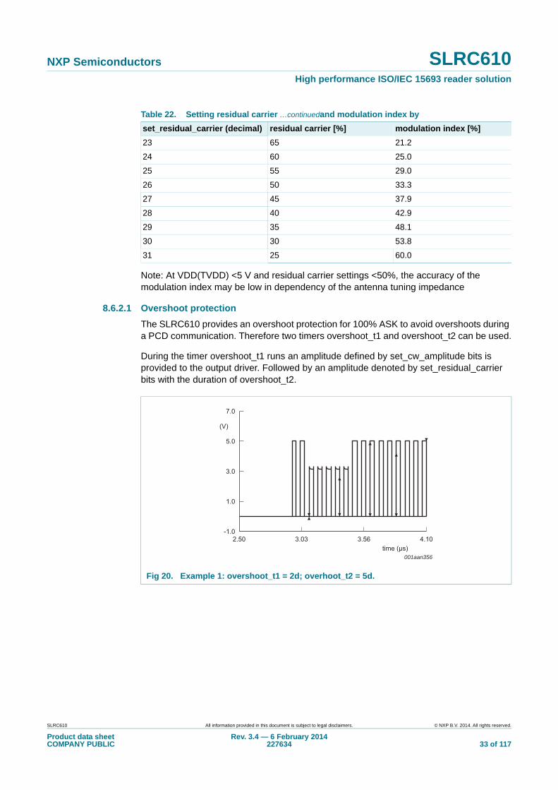
8.6.2.1 Overshoot protection
The SLRC610 provides an overshoot protection for 100% ASK to avoid overshoots during a PCD communication. Therefore two timers overshoot_t1 and overshoot_t2 can be used.
During the timer overshoot_t1 runs an amplitude defined by set_cw_amplitude bits is provided to the output driver. Followed by an amplitude denoted by set_residual_carrier bits with the duration of overshoot_t2.
23 65 21.2
24 60 25.0
25 55 29.0
26 50 33.3
27 45 37.9
28 40 42.9
29 35 48.1
30 30 53.8
31 25 60.0
Table 22. Setting residual carrier …continuedand modulation index by
set_residual_carrier (decimal) residual carrier [%] modulation index [%]
Fig 20. Example 1: overshoot_t1 = 2d; overhoot_t2 = 5d.
001aan356
2.50 3.03 3.56 4.10time (μs)
7.0
5.0
(V)
3.0
1.0
-1.0
SLRC610 All information provided in this document is subject to legal disclaimers. © NXP B.V. 2014. All rights reserved.
Product data sheetCOMPANY PUBLIC
Rev. 3.4 — 6 February 2014227634 33 of 117

NXP Semiconductors SLRC610High performance ISO/IEC 15693 reader solution
8.6.2.2 Bit generator
The default coding of a data stream is done by using the Bit-Generator. It is activated when the value of TxFrameCon.DCodeType is set to 0000 (bin). The Bit-Generator encodes the data stream byte-wise and can apply the following encoding steps to each data byte.
1. Add a start-bit of specified type at beginning of every byte
2. Add a stop-bit and EGT bits of a specified type. The maximum number of EGT bit is 6, only full bits are supported
3. Add a parity-bit of a specified type
4. TxFirstBits (skips a given number of bits at the beginning of the first byte in a frame)
5. TxLastBits (skips a given number of bits at the end of the last byte in a frame)
6. Encrypt data-bit (MIFARE encryption)
TxFirstBits and TxLastBits can be used at the same time. If only a single data byte is sent, it must be ensured that the range of TxFirstBits and TxLastBits do not overlap. It is not possible to skip more than 8 bit of a single byte! ( (8 - TxFirstBits) + (8 - TxLastBits) ) < 8
By default, data bytes are always treated LSB first. To make use of a MSB first coding, the TxMSBFirst in the register CLCON1 needs to be set.
8.6.3 Receiver circuitry
8.6.3.1 General
The SLRC610 features a versatile quadrature receiver architecture with fully differential signal input at RXP and RXN. It can be configured to achieve optimum performance for reception of various 13.56 MHz based protocols.
For all processing units various adjustments can be made to obtain optimum performance.
Fig 21. Example 2: overshoot_t1 = 0d; overhoot_t2 = 5d
0-1.0
1 2 3 4t
1.0
3.0
5.0
(V)
7.0
SLRC610 All information provided in this document is subject to legal disclaimers. © NXP B.V. 2014. All rights reserved.
Product data sheetCOMPANY PUBLIC
Rev. 3.4 — 6 February 2014227634 34 of 117

NXP Semiconductors SLRC610High performance ISO/IEC 15693 reader solution
8.6.3.2 Block diagram
Figure 22 shows the block diagram of the receiver circuitry. The receiving process includes several steps. First the quadrature demodulation of the carrier signal of 13.56 MHz is done. Several tuning steps in this circuit are possible.
The receiver can also be operated in a single ended mode. In this case the Rcv_RX_single bit has to be set. In the single ended mode, the two receiver pins RXP and RXN need to be connected together and will provide a single ended signal to the receiver circuitry.
When using the receiver in a single ended mode the receiver sensitivity is decreased and the achievable reading distance might be reduced, compared to the fully differential mode.
The quadrature-demodulator uses two different clocks, Q-clock and I-clock, with a phase shift of 90 between them. Both resulting baseband signals are amplified, filtered, digitized and forwarded to a correlation circuitry.
The typical application is intended to implement the Fully differential mode and will deliver maximum reader/writer distance. The Quasi differential mode can be used together with dedicated antenna topologies that allow a reduction of matching components at the cost of overall reading performance.
Fig 22. Block diagram of receiver circuitry
Table 23. Configuration for single or differential receiver
Mode rcv_rx_single pins RXP and RXN
Fully differential 0 provide differential signal from differential antenna by separate rx-coupling branches
Quasi differential 1 connect RXP and RXN together and provide single ended signal from antenna by a single rx-coupling branch
001aan358
13.56 MHzI/O CLOCK
GENERATION
I-clks
Q-clks
clk_27 MHzTIMING
GENERATIONADC
DATA
DATA
Adc_data_readyclk_27 MHz
mixer mix_out_i_p
2-stage BBA
mix_out_i_n
out_i_p
out_i_n
rx_p
rx_n
rx_p
rx_n
mixer
mix_out_q_p2-stage BBA
mix_out_q_n
out_q_p
out_q_n
rcv_gain<1:0>
rcv_hpcf<1:0>fully/quasi-differential
fully/quasi-differential
rcv_gain<1:0>
rcv_hpcf<1:0>
rx_p
rx_n
SLRC610 All information provided in this document is subject to legal disclaimers. © NXP B.V. 2014. All rights reserved.
Product data sheetCOMPANY PUBLIC
Rev. 3.4 — 6 February 2014227634 35 of 117

NXP Semiconductors SLRC610High performance ISO/IEC 15693 reader solution
During low power card detection the DC levels at the I- and Q-channel mixer outputs are evaluated. This requires that mixers are directly connected to the ADC. This can be configured by setting the bit Rx_ADCmode in register Rcv (38h).
8.6.4 Active antenna concept
Two main blocks are implemented in the SLRC610. A digital circuitry, comprising state machines, coder and decoder logic and an analog circuitry with the modulator and antenna drivers, receiver and amplification circuitry. For example, the interface between these two blocks can be configured in the way, that the interfacing signals may be routed to the pins SIGIN and SIGOUT. The most important use of this topology is the active antenna concept where the digital and the analog blocks are separated. This opens the possibility to connect e.g. an additional digital block of another SLRC610 device with a single analog antenna front-end.
The Table 24 and Table 25 describe the necessary register configuration for the use case active antenna concept.
The interface between these two blocks can be configured in the way, that the interfacing signals may be routed to the pins SIGIN and SIGOUT (see Figure 24 “Overview SIGIN/SIGOUT Signal Routing”).
This topology supports, that some parts of the analog part of the SLRC610 may be connected to the digital part of another device.
The switch SigOutSel in registerSigOut can be used to measure signals. This is especially important during the design In phase or for test purposes to check the transmitted and received data.
Fig 23. Block diagram of the active Antenna concept
Table 24. Register configuration of SLRC610 active antenna concept (DIGITAL)
Register Value (binary) Description
SigOut.SigOutSel 0100 TxEnvelope
Rcv.SigInSel 11 Receive over SigIn (Generic Code)
DrvCon.TxSel 00 Low (idle)
Table 25. Register configuration of SLRC610 active antenna concept (Antenna)
Register Value (binary) Description
SigOut.SigOutSel 0110 Generic Code (Manchester)
Rcv.SigInSel 01 Internal
DrvCon.TxSel 10 External (SigIn)
RxCtrl.RxMultiple 1 RxMultiple on
001aam307
SIGIN
SIGINSIGOUT
SIGOUTREADER IC(DIGITAL)
READER IC(ANTENNA)
SLRC610 All information provided in this document is subject to legal disclaimers. © NXP B.V. 2014. All rights reserved.
Product data sheetCOMPANY PUBLIC
Rev. 3.4 — 6 February 2014227634 36 of 117

NXP Semiconductors SLRC610High performance ISO/IEC 15693 reader solution
However, the most important use of SIGIN/SIGOUT pins is the active antenna concept. An external active antenna circuit can be connected to the digital circuit of the SLRC610. SigOutSel has to be configured in that way that the signal of the internal Miller Coder is sent to SIGOUT pin (SigOutSel = 4). SigInSel has to be configured to receive Manchester signal with sub-carrier from SIGIN pin (SigInSel = 1).
It is possible, to connect a passive antenna to pins TX1, TX2 and RX (via the appropriate filter and matching circuit) and at the same time an active antenna to the pins SIGOUT and SIGIN. In this configuration, two RF-parts may be driven (one after another) by a single host processor.
SLRC610 All information provided in this document is subject to legal disclaimers. © NXP B.V. 2014. All rights reserved.
Product data sheetCOMPANY PUBLIC
Rev. 3.4 — 6 February 2014227634 37 of 117

xxxxxxxxxxxxxxxxxxxxx xxxxxxxxxxxxxxxxxxxxxxxxxx xxxxxxx x x x xxxxxxxxxxxxxxxxxxxxxxxxxxxxxx xxxxxxxxxxxxxxxxxxx xx xx xxxxx xxxxxxxxxxxxxxxxxxxxxxxxxxx xxxxxxxxxxxxxxxxxxx xxxxxx xxxxxxxxxxxxxxxxxxxxxxxxxxxxxxxxxxx xxxxxxxxxxxx x x xxxxxxxxxxxxxxxxxxxxx xxxxxxxxxxxxxxxxxxxxxxxxxxxxxx xxxxx xxxxxxxxxxxxxxxxxxxxxxxxxxxxxxxxxxxxxxxxxxxxxxxxxx xxxxxxxx xxxxxxxxxxxxxxxxxxxxxxxxx xxxxxxxxxxxxxxxxxxxx xxx
SL
RC
610
Pro
du
ct data sh
CO
MP
AN
Y P
UB
L
NX
P S
emico
nd
ucto
rsS
LR
C610
Hig
h p
erform
an
ce
ISO
/IEC
15
693 rea
der s
olu
tion
001aam001
SIGOUT
ANALOG MODULE
MODULATOR DRIVERTX2
TX1
RXNRXP
DEMODULATOR
All inform
ation provided
in this docum
ent is subject to leg
al disclaim
ers.©
NX
P B
.V. 2014. A
ll rights reserved.
eetIC
Rev. 3.4 —
6 Feb
ruary 2014
227634 38 o
f 117
Fig 24. Overview SIGIN/SIGOUT Signal Routing
CODER SIGOUTSel[4:0]
Sigpro_in_sel[1:0]
SIGIN
TX bit stream
DIGITAL MODULE
RX bit stream
0, 1234567
9
tri-stateLOWHIGH
TX envelopeTX active
S3C signalRX envelope
8RX activeRX bit signal
DECODER
SUBCARRIERDEMODULATOR
TxCon.TxSel[1:0]
0123
No_nodulationTX envelope
RFUSIGIN
0123
tri-stateinternal analog blockSIGIN over envelopeSIGIN generic

NXP Semiconductors SLRC610High performance ISO/IEC 15693 reader solution
8.6.5 Symbol generator
The symbol generator is used to create various protocol symbols like the CS symbol as used by the ICODE EPC protocol.
Symbols are defined by means of the symbol definition registers and the mode registers. Four different symbols can be used. Two of them, Symbol0 and Symbol1 have a maximum pattern length of 16 bit and feature a burst length of up to 256 bits of either logic “0” or logic “1”. The Symbol2 and Symbol3 are limited to 8 bit pattern length and do not support a burst.
The definition of symbol patterns is done by writing the bit sequence of the pattern to the appropriate register. The last bit of the pattern to be sent is located at the LSB of the register. By setting the symbol length in the symbol-length register (TxSym10Len and TxSym32Len) the definition of the symbol pattern is completed. All other bits at bit-position higher than the symbol length in the definition register are ignored. (Example: length of Symbol2 = 5, bit7 and bit6 are ignored, bit5 to bit0 define the symbol pattern, bit5 is sent first)
Which symbol-pattern is sent can be configured in the TxFrameCon register. Symbol0, Symbol1 and Symbol2 can be sent before data packets, Symbol1, Symbol2 and Symbol3 can be sent after data packets. Each symbol is defined by a set of registers. Symbols are configured by a pair of registers. Symbol0 and Symbol1 share the same configuration and Symbol2 and Symbol3 share the same configuration. The configuration includes setting of bit-clock- and subcarrier-frequency, as well as selection of the pulse type/length and the envelope type.
8.7 Memory
8.7.1 Memory overview
The SLRC610 implements three different memories: EEPROM, FIFO and Registers.
At startup, the initialization of the registers which define the behavior of the IC is performed by an automatic copy of an EEPROM area (read/write EEPROM section1 and section2, register reset) into the registers. The behavior of the SLRC610 can be changed by executing the command LoadProtocol, which copies a selected default protocol from the EEPROM (read only EEPROM section4, register Set Protocol area) into the registers.
The read/write EEPROM section2 can be used to store any user data or predefined register settings. These predefined settings can be copied with the command "LoadRegister" into the internal registers.
The FIFO is used as Input/Out buffer and is able to improve the performance of a system with limited interface speed.
SLRC610 All information provided in this document is subject to legal disclaimers. © NXP B.V. 2014. All rights reserved.
Product data sheetCOMPANY PUBLIC
Rev. 3.4 — 6 February 2014227634 39 of 117

NXP Semiconductors SLRC610High performance ISO/IEC 15693 reader solution
8.7.2 EEPROM memory organization
The SLRC610 has implemented a EEPROM non-volatile memory with a size of 8 kB.The EEPROM is organized in pages of 64 bytes. One page of 64 bytes can be programmed at a time. Defined purposes had been assigned to specific memory areas of the EEPROM, which are called Sections. Five sections 0..4 with different purpose do exist.
The following figure show the structure of the EEPROM:
Table 26. EEPROM memory organization
Section Page Byte addresses
Access rights
Memory content
0 0 00 to 31 r product information and configuration
32 to 63 r/w product configuration
1 1 to 2 64 to 191 r/w register reset
2 3 to 111 192 to 7167 r/w free
3 112 to 128 7168 to 8191 r Register Set Protocol (RSP)
Fig 25. Sector arrangement of the EEPROM
aaa-002467
Production and configSection 0:
Register resetSection 1:
FreeSection 2:
RSP-Area for TXSection 3_TX:
RSP-Area for RXSection 3_RX:
SLRC610 All information provided in this document is subject to legal disclaimers. © NXP B.V. 2014. All rights reserved.
Product data sheetCOMPANY PUBLIC
Rev. 3.4 — 6 February 2014227634 40 of 117

NXP Semiconductors SLRC610High performance ISO/IEC 15693 reader solution
8.7.2.1 Product information and configuration - Page 0
The first EEPROM page includes production data as well as configuration information.
ProductID: Identifier for this SLRC610 product, only address 01h shall be evaluated for identifying the Product CLRC663, address 00h and 02h shall be ignored by software.
Version: This register indicates the version of the EEPROM initialization data during production. (Identification of the Hardware version is available in the register 7Fh, not in the EEPROM Version address. The hardware information in register 7Fh is hardwired and therefore independent from any EEPROM configuration.)
Unique identifier: Unique identifier for this device
Manufacturer Data: This data is programmed during production. The content is not intended to be used by any application and might be not the same for different devices. Therefore this content needs to be considered to be undefined.
I2C-Address: Two possibilities exist to define the address of the I2C interface. This can be done either by configuring the pins IF0, IF2 (address is then 10101xx, xx is defined by the interface pins IF0, IF2) or by writing value into the I2C address area. The selection, which of this 2-information pin configuration or EEPROM content - is used as I2C-address is done at EEPROM address 21h (Interface, bit4)
Interface: This section describes the interface byte configuration.
Table 27. Production area (Page 0)
Address (Hex.)
0 1 2 3 4 5 6 7
00 ProductID Version Unique Identifier
08 Unique Identifier ManufacturerData
10 ManufacturerData
18 ManufacturerData
Table 28. Product ID overview of CLRC663 family
Address 01h Product ID
CLRC663 01h
MFRC631 C0h
MFRC630 80h
SLRC610 20h
Table 29. Configuration area (Page 0)
Address (Hex.)
0 1 2 3 4 5 6 7
20 I2C_Address Interface I2C SAM_Address DefaultProtRx DefaultProtTx - TxCRCPreset
28 RxCRCPreset - - - - - -
30 -
38 -
SLRC610 All information provided in this document is subject to legal disclaimers. © NXP B.V. 2014. All rights reserved.
Product data sheetCOMPANY PUBLIC
Rev. 3.4 — 6 February 2014227634 41 of 117
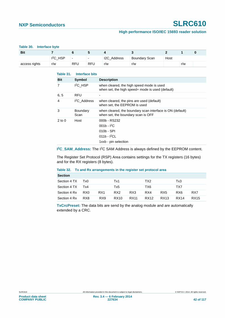
NXP Semiconductors SLRC610High performance ISO/IEC 15693 reader solution
I2C_SAM_Address: The I2C SAM Address is always defined by the EEPROM content.
The Register Set Protocol (RSP) Area contains settings for the TX registers (16 bytes) and for the RX registers (8 bytes).
TxCrcPreset: The data bits are send by the analog module and are automatically extended by a CRC.
Table 30. Interface byte
Bit 7 6 5 4 3 2 1 0
I2C_HSP - - I2C_Address Boundary Scan Host
access rights r/w RFU RFU r/w r/w r/w
Table 31. Interface bits
Bit Symbol Description
7 I2C_HSP when cleared, the high speed mode is usedwhen set, the high speed+ mode is used (default)
6, 5 RFU -
4 I2C_Address when cleared, the pins are used (default)when set, the EEPROM is used
3 Boundary Scan
when cleared, the boundary scan interface is ON (default)when set, the boundary scan is OFF
2 to 0 Host 000b - RS232
001b - I2C
010b - SPI
011b - I2CL
1xxb - pin selection
Table 32. Tx and Rx arrangements in the register set protocol area
Section
Section 4 TX Tx0 Tx1 TX2 Tx3
Section 4 TX Tx4 Tx5 TX6 TX7
Section 4 Rx RX0 RX1 RX2 RX3 RX4 RX5 RX6 RX7
Section 4 Rx RX8 RX9 RX10 RX11 RX12 RX13 RX14 RX15
SLRC610 All information provided in this document is subject to legal disclaimers. © NXP B.V. 2014. All rights reserved.
Product data sheetCOMPANY PUBLIC
Rev. 3.4 — 6 February 2014227634 42 of 117

NXP Semiconductors SLRC610High performance ISO/IEC 15693 reader solution
8.7.3 EEPROM initialization content LoadProtocol
The SLRC610 EEPROM is initialized at production with values which are used to reset certain registers of the SLRC610 to default settings by copying the EEprom content to the registers. Only registers or bits with “read/write” or “dynamic” access rights are initialized with this default values copied from the EEProm.
Note that the addresses used for copying reset values from EEprom to registers are dependent on the configured protocol and can be changed by the user.
The register reset values are configuration parameters used after startup of the IC. They can be changed to modify the default behavior of the device. In addition to this register reset values, is the possibility to load settings for various user implemented protocols.The load protocol command is used for this purpose.
Table 33. Register reset values (Hex.) (Page0)
Address 0 (8) 1 (9) 2 (A) 3 (B) 4 (C) 5 (D) 6 (E) 7 (F)
Function Product ID Version Unique Serial Number
00 XX see table 34 XX XX XX XX XX XX
Function Unique Serial Number Factory trim value
08 XX XX XX XX XX XX XX XX
Function TrimLFO Factory trim values
10 XX XX XX XX XX XX XX XX
Function Factory trim values
18.... XX XX XX XX XX XX XX XX
Factory trim values
....38 XX XX XX XX XX XX XX XX
Table 34. Register reset values (Hex.)(Page1 and page 2)
Address 0 (8) 1 (9) 2 (A) 3 (B) 4 (C) 5 (D) 6 (E) 7 (F)
Command HostCtrl FiFoControl WaterLevel FiFoLength FiFoData IRQ0 IRQ1
40 40 00 80 05 00 00 00 00
IRQ0En IRQ1En Error Status RxBitCtrl RxColl TControl T0Control
48 10 00 00 00 00 00 00 00
T0ReloadHi T0ReloadLo T0CounterValHi
T0CounterValLo
T1Control T1ReloadHi T1ReloadLo T1CounterValHi
50 00 80 00 00 00 00 80 00
T1CounterValLo
T2Control T2ReloadHi T2ReloadLo T2CounterValHi
T2CounterValLo
T3Control T3ReloadHi
58 00 00 00 80 00 00 00 00
T3ReloadLo T3CounterValHi
T3CounterValHi
T4Control T4ReloadHi T4ReloadLo T4CounterValHi
T4CounterValLo
60 80 00 00 00 00 80 00 00
SLRC610 All information provided in this document is subject to legal disclaimers. © NXP B.V. 2014. All rights reserved.
Product data sheetCOMPANY PUBLIC
Rev. 3.4 — 6 February 2014227634 43 of 117

NXP Semiconductors SLRC610High performance ISO/IEC 15693 reader solution
DrvMode TxAmp DrvCon Txl TxCRCPreset
RxCRCPreset
TxDataNum TxModWith
68 86 15 11 06 18 18 08 27
TxSym10BurstLen
TxWaitCtrl TxWaitLo FrameCon RxSofD RxCtrl RxWait RxThreshold
70 00 C0 12 CF 00 04 90 3F
Rcv RxAna RFU SerialSpeed LFO_trimm PLL_Ctrl PLL_Div LPCD_QMin
78 12 0A 00 7A 80 04 20 48
LPCD_QMax
LPCD_IMin LPCD _result_I
LPCD _result_Q
PadEn PadOut PadIn SigOut
80 12 88 00 00 00 00 00 00
TxBitMod RFU TxDataCon TxDataMod TxSymFreq TxSym0H TySym0L TxSym1H
88 20 xx 04 50 40 00 00 00
Table 34. Register reset values (Hex.)(Page1 and page 2) …continued
Address 0 (8) 1 (9) 2 (A) 3 (B) 4 (C) 5 (D) 6 (E) 7 (F)
SLRC610 All information provided in this document is subject to legal disclaimers. © NXP B.V. 2014. All rights reserved.
Product data sheetCOMPANY PUBLIC
Rev. 3.4 — 6 February 2014227634 44 of 117

NXP Semiconductors SLRC610High performance ISO/IEC 15693 reader solution
8.8 Clock generation
8.8.1 Crystal oscillator
The clock applied to the SLRC610 acts as time basis for generation of the carrier sent out at TX and for the quadrature mixer I and Q clock generation as well as for the coder and decoder of the synchronous system. Therefore stability of the clock frequency is an important factor for proper performance. To obtain highest performance, clock jitter has to be as small as possible. This is best achieved by using the internal oscillator buffer with the recommended circuitry.
8.8.2 IntegerN PLL clock line
The SLRC610 is able to provide a clock with configurable frequency at CLKOUT from 1 MHz to 24 MHz (PLL_Ctrl and PLL_DIV). There it can serve as a clock source to a microcontroller which avoids the need of a second crystal oscillator in the reader system. Clock source for the IntegerN-PLL is the 27.12 MHz crystal oscillator.
Two dividers are determining the output frequency. First a feedback integer-N divider configures the VCO frequency to be N fin/2 (control signal pll_set_divfb). As supported Feedback Divider Ratios are 23, 27 and 28, VCO frequencies can be 23 fin / 2 (312 MHz), 27 fin / 2 (366 MHz) and 28 fin / 2 (380 MHz).
The VCO frequency is divided by a factor which is defined by the output divider (pll_set_divout). Table 36 “Divider values for selected frequencies using the integerN PLL” shows the accuracy achieved for various frequencies (integer multiples of 1 MHz and some typical RS232 frequencies) and the divider ratios to be used. The register bit ClkOutEn enables the clock at CLKOUT pin.
The following formula can be used to calculate the output frequency:
Fig 26. Quartz connection
Table 35. Crystal requirements recommendations
Symbol Parameter Conditions Min Typ max Unit
fxtal crystal frequency - 27.12 - MHz
fxtal/fxtal relative crystal frequency variation
250 - +250 ppm
ESR equivalent series resistance
- 50 100
CL load capacitance - 10 - pF
Pxtal crystal power dissipation
- 50 100 W
001aam308
27.12 MHz
XTAL1 XTAL2
READER IC
SLRC610 All information provided in this document is subject to legal disclaimers. © NXP B.V. 2014. All rights reserved.
Product data sheetCOMPANY PUBLIC
Rev. 3.4 — 6 February 2014227634 45 of 117
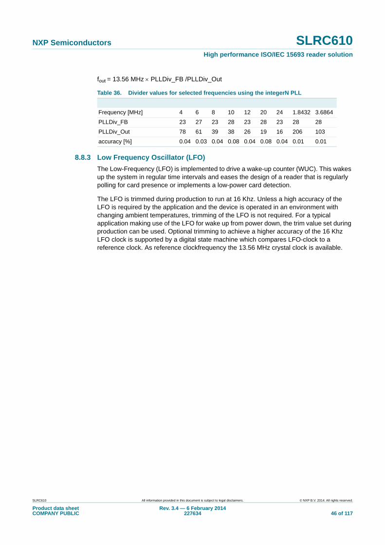
NXP Semiconductors SLRC610High performance ISO/IEC 15693 reader solution
fout = 13.56 MHz PLLDiv_FB /PLLDiv_Out
8.8.3 Low Frequency Oscillator (LFO)
The Low-Frequency (LFO) is implemented to drive a wake-up counter (WUC). This wakes up the system in regular time intervals and eases the design of a reader that is regularly polling for card presence or implements a low-power card detection.
The LFO is trimmed during production to run at 16 Khz. Unless a high accuracy of the LFO is required by the application and the device is operated in an environment with changing ambient temperatures, trimming of the LFO is not required. For a typical application making use of the LFO for wake up from power down, the trim value set during production can be used. Optional trimming to achieve a higher accuracy of the 16 Khz LFO clock is supported by a digital state machine which compares LFO-clock to a reference clock. As reference clockfrequency the 13.56 MHz crystal clock is available.
Table 36. Divider values for selected frequencies using the integerN PLL
Frequency [MHz] 4 6 8 10 12 20 24 1.8432 3.6864
PLLDiv_FB 23 27 23 28 23 28 23 28 28
PLLDiv_Out 78 61 39 38 26 19 16 206 103
accuracy [%] 0.04 0.03 0.04 0.08 0.04 0.08 0.04 0.01 0.01
SLRC610 All information provided in this document is subject to legal disclaimers. © NXP B.V. 2014. All rights reserved.
Product data sheetCOMPANY PUBLIC
Rev. 3.4 — 6 February 2014227634 46 of 117

NXP Semiconductors SLRC610High performance ISO/IEC 15693 reader solution
8.9 Power management
8.9.1 Supply concept
The SLRC610 is supplied by VDD (Supply Voltage), PVDD (Pad Supply) and TVDD (Transmitter Power Supply). These three voltages are independent from each other.
To connect the SLRC610 to a Microcontroller supplied by 3.3 V, PVDD and VDD shall be at a level of 3.3 V, TVDD can be in a range from 3.3 V to 5.0 V. A higher supply voltage at TVDD will result in a higher field strength.
Independent of the voltage it is recommended to buffer these supplies with blocking capacitances close to the terminals of the package. VDD and PVDD are recommended to be blocked with a capacitor of 100 nF min, TVDD is recommended to be blocked with 2 capacitors, 100 nF parallel to 1.0 F
AVDD and DVDD are not supply input pins. They are output pins and shall be connected to blocking capacitors 470 nF each.
8.9.2 Power reduction mode
8.9.2.1 Power-down
A hard power-down is enabled with HIGH level on pin PDOWN. This turns off the internal 1.8 V voltage regulators for the analog and digital core supply as well as the oscillator. All digital input buffers are separated from the input pads and clamped internally (except pin PDOWN itself). The output pins are switched to high impedance.
To leave the power-down mode the level at the pin PDOWN as to be set to LOW. This will start the internal start-up sequence.
8.9.2.2 Standby mode
The standby mode is entered immediately after setting the bit PowerDown in the register Command. All internal current sinks are switched off except the LFO. Voltage references and voltage regulators will be set into stand-by mode.
In opposition to the power-down mode, the digital input buffers are not separated by the input pads and keep their functionality. The digital output pins do not change their state.
During standby mode, all registers values, the FIFO’s content and the configuration itself will keep its current content.
To leave the standby mode the bit PowerDown in the register Command is cleared. This will trigger the internal start-up sequence. The reader IC is in full operation mode again when the internal start-up sequence is finalized (the typical duration is 15 us).
Alternatively, a value of 55h can be sent to the SLRC610 using the RS232 interface to leave the standby mode. Then read accesses shall be performed at address 00h until the device returns the content of this address. The return of the content of address 00h indicates that the device is ready to receive further commands and the internal start-up sequence is finalized.
8.9.2.3 Modem off mode
When the ModemOff bit in the register Control is set the antenna transmitter and the receiver are switched off.
SLRC610 All information provided in this document is subject to legal disclaimers. © NXP B.V. 2014. All rights reserved.
Product data sheetCOMPANY PUBLIC
Rev. 3.4 — 6 February 2014227634 47 of 117

NXP Semiconductors SLRC610High performance ISO/IEC 15693 reader solution
To leave the modem off mode clears the ModemOff bit in the register Control.
8.9.3 Low-Power Card Detection (LPCD)
The low-power card detection is an energy saving mode in which the SLRC610 is not fully powered permanently.
The LPCD works in two phases. First the standby phase is controlled by the wake-up counter (WUC), which defines the duration of the standby of the SLRC610. Second phase is the detection-phase. In this phase the values of the I and Q channel are detected and stored in the register map. (LPCD_I_Result, LPCD_Q_Result).This time period can be handled with Timer3. The value is compared with the min/max values in the registers (LPCD_IMin, LPCD_IMax; LPCD_QMin, LPCD_QMax). If it exceeds the limits, a LPCDIrq is raised.
After the command LPCD the standby of the SLRC610 is activated, if selected. The wake-up Timer4 can activate the system after a given time. For the LPCD it is recommended to set T4AutoWakeUp and T4AutoRestart, to start the timer and then go to standby. If a card is detected the timer stops and the communication can be started. If T4AutoWakeUp is not set, the IC will not enter Standby mode in case no card is detected.
8.9.4 Reset and start-up time
A 10 s constant high level at the PDOWN pin starts the internal reset procedure.
The following figure shows the internal voltage regulator:
When the SLRC610 has finished the reset phase and the oscillator has entered a stable working condition the IC is ready to be used.
Fig 27. Internal PDown to voltage regulator logic
001aan360
PVDD
PDown
VSS
GLITCHFILTER
INTERNAL VOLTAGEREGULATOR
VDD
VSS
1.8 V
1.8 V
AVDD
DVDD
SLRC610 All information provided in this document is subject to legal disclaimers. © NXP B.V. 2014. All rights reserved.
Product data sheetCOMPANY PUBLIC
Rev. 3.4 — 6 February 2014227634 48 of 117

NXP Semiconductors SLRC610High performance ISO/IEC 15693 reader solution
8.10 Command set
8.10.1 General
The behavior is determined by a state machine capable to perform a certain set of commands. By writing the according command-code to register Command the command is executed.
Arguments and/or data necessary to process a command, are exchanged via the FIFO buffer.
• A data transmission of the TxEncoder can be started by a command. When started, the communication is executed as defined in the TxFrameCon register. Therefore a communication frame can consist of a start-symbol, a data-stream, and followed by an end-symbol.
• Each command that needs a certain number of arguments will start processing only when it has received the correct number of arguments via the FIFO buffer.
• The FIFO buffer is not cleared automatically at command start. Therefore, it is recommended to write the command arguments and/or the data bytes into the FIFO buffer and start the command afterwards.
• Each command may be interrupted by the host by writing a new command code into register Command e.g.: the Idle-Command.
8.10.2 Command set overview
Table 37. Command set
Command No. Parameter (bytes) Short description
Idle 00h - no action, cancels current command execution
LPCD 01h - low-power card detection
AckReq 04h - performs a query, an Ack and a Req-Rn for ISO/IEC 18000-3 mode 3/ EPC Class-1 HF
Receive 05h - activates the receive circuit
Transmit 06h - transmits data from the FIFO buffer
Transceive 07h - transmits data from the FIFO buffer and automatically activates the receiver after transmission finished
WriteE2 08h addressL, addressH, data; gets one byte from FIFO buffer and writes it to the internal EEPROM, valid address range are the addresses of the MIFARE Key area
WriteE2Page 09h (page Address), data0, [data1 ..data63];
gets up to 64 bytes (one EEPROM page) from the FIFO buffer and writes it to the EEPROM, valid page address range are the pages of the MIFARE Key Area
ReadE2 0Ah addressL, address H, length; reads data from the EEPROM and copies it into the FIFO buffer, valid address range are the addresses of the MIFARE Key area
LoadReg 0Ch (EEPROM addressL), (EEPROM addressH), RegAdr, (number of Register to be copied);
reads data from the internal EEPROM and initializes the SLRC610 registers. EEPROM address needs to be within EEPROM sector 2
SLRC610 All information provided in this document is subject to legal disclaimers. © NXP B.V. 2014. All rights reserved.
Product data sheetCOMPANY PUBLIC
Rev. 3.4 — 6 February 2014227634 49 of 117

NXP Semiconductors SLRC610High performance ISO/IEC 15693 reader solution
8.10.3 Command functionality
8.10.3.1 Idle command
Command (00h);
This command indicates that the SLRC610 is in idle mode. This command is also used to terminate the actual command.
8.10.3.2 LPCD command
Command (01h);
This command performs a low-power card detection and or an automatic trimming of the LFO. The values of the sampled I and Q channel are stored in the register map. The value is compared with the min/max values in the register. If it exceeds the limits, an LPCD_Irq will be raised. After the command the standby is activated if selected.
8.10.3.3 AckReq command
Command (04h);
Performs a Query (Full command must be written into the FIFO); a Ack and a ReqRn command. All answers to the command will be written into the FIFO. The error flag is copied after the answer into the FIFO.
This command terminates automatically when finished and the active command is idle.
8.10.3.4 Receive command
Command (05h);
The SLRC610 activates the receiver path, waits for any data stream to be received, according to its register settings, which shall be set before starting this command according the used protocol and antenna configuration. The correct settings have to be chosen before starting this command.
This command terminates automatically when the received data stream ends. This is indicated either by the end of frame pattern or by the length byte depending on the selected framing and speed.
Remark: If the bit RxMultiple in the RxModeReg register is set to logic 1, the Receive command does not terminate automatically. It has to be terminated by activating any other command in the CommandReg register (see Section 0.2.6 “RxMod”).
8.10.3.5 Transmit command
Command (06h);
LoadProtocol 0Dh (Protocol umber RX), (Protocol number TX);
reads data from the internal EEPROM and initializes the SLRC610 registers needed for a Protocol change
ReadRNR 1Ch - Copies bytes from the Random Number generator into the FIFO until the FiFo is full
Soft Reset 1Fh - resets the SLRC610
Table 37. Command set …continued
Command No. Parameter (bytes) Short description
SLRC610 All information provided in this document is subject to legal disclaimers. © NXP B.V. 2014. All rights reserved.
Product data sheetCOMPANY PUBLIC
Rev. 3.4 — 6 February 2014227634 50 of 117

NXP Semiconductors SLRC610High performance ISO/IEC 15693 reader solution
The content of the FIFO is transmitted immediately after starting the command. Before transmitting the FIFO content all relevant register have to be set to transmit data.
This command terminates automatically when the FIFO gets empty. It can be terminated by any other command written to the command register.
8.10.3.6 Transceive command
Command (07h);
This command transmits data from the FIFO and receives data from the RF field at once. The first action is transmitting and after a transmission the command is changed to receive a data stream.
Each transmission process starts by writing the command into CommandReg.
Remark: If the bit RxMultiple in register RxModeReg is set to logic 1, this command will never leave the receiving state, because the receiving will not be cancelled automatically.
8.10.3.7 WriteE2 command
Command (08h), Parameter1 (addressL), Parameter2 (addressH), Parameter3 (data);
This command writes one byte into the EEPROM. If the FIFO contains no data, the command will wait until the data is available.
Abort condition: insufficient parameter in FIFO; Address-parameter outside of range.
8.10.3.8 WriteE2PAGE command
Command (09h), Parameter1 (page address), Parameter2 (data0), Parameter3...65 [data1 ..data63];
This command writes up to 64 bytes into the EEPROM.
Abort condition: Insufficient parameters in FIFO; Page address parameter outside of range.
8.10.3.9 ReadE2 command
Command (0Ah), Parameter1 (addressL), Parameter2 (addressH), Parameter3 (length);
Reads up to 256 bytes from the EEPROM to the FIFO. If a read operation exceeds the address 1FFFh, the read operation continues from address 0000h.
Abort condition: Insufficient parameter in FIFO; Address parameter outside of range.
8.10.3.10 LoadReg command
Command (0Ch), Parameter1 (EEPROM addressL),Parameter2 (EEPROM addressH), Parameter3 (RegAdr), Parameter4 (number);
Read a defined number of bytes from the EEPROM and copies the value into the Register set, beginning at the given address RegAdr.
Abort condition: Insufficient parameter in FIFO; Address parameter outside of range.
8.10.3.11 LoadProtocol command
Command (0Dh), Parameter1 (Protocol number RX), Parameter2 (Protocol number TX);
SLRC610 All information provided in this document is subject to legal disclaimers. © NXP B.V. 2014. All rights reserved.
Product data sheetCOMPANY PUBLIC
Rev. 3.4 — 6 February 2014227634 51 of 117

NXP Semiconductors SLRC610High performance ISO/IEC 15693 reader solution
Reads out the EEPROM Register Set Protocol Area and overwrites the content of the Rx- and Tx- related registers. These registers are important for a Protocol selection.
Abort condition: Insufficient parameter in FIFO
[1] For more protocol details please refer to Section 8 “Functional description”.
[1] For more protocol details please refer to Section 8 “Functional description”.
8.10.3.12 GetRNR command
Command (1Ch);
This command is reading Random Numbers from the random number generator of the SLRC610. The Random Numbers are copied to the FIFO until the FIFO is full.
8.10.3.13 SoftReset command
Command (1Fh);
Table 38. Predefined protocol overview RX[1]
Protocol Number (decimal)
Protocol Receiver speed [kbits/s]
Receiver Coding
00 ISO/IEC15693 26 SSC
01 ISO/IEC15693 52 SSC
02 ISO/IEC15693 26 DSC
03 EPC/UID 26 SSC
04 ISO/IEC 18000-3 mode 3/EPC Class-1 HF
2/424
05 ISO/IEC 18000-3 mode 3/ EPC Class-1 HF
4/424
06 ISO/IEC 18000-3 mode 3/ EPC Class-1 HF
2/848
07 ISO/IEC 18000-3 mode 3/ EPC Class-1 HF
4/848
Table 39. Predefined protocol overview TX[1]
Protocol Number (decimal)
Protocol Transmitter speed [kbits/s]
Transmitter Coding
00 ISO/IEC15693 26 1/4
01 ISO/IEC15693 26 1/4
02 ISO/IEC15693 1,66 1/256
03 EPC/UID 53 Unitray
04 ISO/IEC 18000-3 mode 3/ EPC Class-1 HF
Tari, ASK, PIE
05 ISO/IEC 18000-3 mode 3/ EPC Class-1 HF
Tari, ASK, PIE
06 ISO/IEC 18000-3 mode 3/ EPC Class-1 HF
Tari, ASK, PIE
07 ISO/IEC 18000-3 mode 3/ EPC Class-1 HF
Tari, ASK, PIE
SLRC610 All information provided in this document is subject to legal disclaimers. © NXP B.V. 2014. All rights reserved.
Product data sheetCOMPANY PUBLIC
Rev. 3.4 — 6 February 2014227634 52 of 117

NXP Semiconductors SLRC610High performance ISO/IEC 15693 reader solution
This command is performing a soft reset. Triggered by this command all the default values for the register setting will be read from the EEPROM and copied into the register set.
SLRC610 All information provided in this document is subject to legal disclaimers. © NXP B.V. 2014. All rights reserved.
Product data sheetCOMPANY PUBLIC
Rev. 3.4 — 6 February 2014227634 53 of 117

NXP Semiconductors SLRC610High performance ISO/IEC 15693 reader solution
9. SLRC610 registers
9.1 Register bit behavior
Depending on the functionality of a register, the access conditions to the register can vary. In principle, bits with same behavior are grouped in common registers. The access conditions are described in Table 40.
Table 40. Behavior of register bits and their designation
Abbreviation Behavior Description
r/w read and write These bits can be written and read via the host interface. Since they are used only for control purposes, the content is not influenced by the state machines but can be read by internal state machines.
dy dynamic These bits can be written and read via the host interface. They can also be written automatically by internal state machines, for example Command register changes its value automatically after the execution of the command.
r read only These register bits indicates hold values which are determined by internal states only.
w write only Reading these register bits always returns zero.
RFU - These bits are reserved for future use and must not be changed. In case of a required write access, it is recommended to write a logic 0.
Table 41. SLRC610 registers overview
Address Register name Function
00h Command Starts and stops command execution
01h HostCtrl Host control register
02h FIFOControl Control register of the FIFO
03h WaterLevel Level of the FIFO underflow and overflow warning
04h FIFOLength Length of the FIFO
05h FIFOData Data In/Out exchange register of FIFO buffer
06h IRQ0 Interrupt register 0
07h IRQ1 Interrupt register 1
08h IRQ0En Interrupt enable register 0
09h IRQ1En Interrupt enable register 1
0Ah Error Error bits showing the error status of the last command execution
0Bh Status Contains status of the communication
0Ch RxBitCtrl Control register for anticollision adjustments for bit oriented protocols
0Dh RxColl Collision position register
0Eh TControl Control of Timer 0..3
0Fh T0Control Control of Timer0
10h T0ReloadHi High register of the reload value of Timer0
11h T0ReloadLo Low register of the reload value of Timer0
12h T0CounterValHi Counter value high register of Timer0
13h T0CounterValLo Counter value low register of Timer0
SLRC610 All information provided in this document is subject to legal disclaimers. © NXP B.V. 2014. All rights reserved.
Product data sheetCOMPANY PUBLIC
Rev. 3.4 — 6 February 2014227634 54 of 117

NXP Semiconductors SLRC610High performance ISO/IEC 15693 reader solution
14h T1Control Control of Timer1
15h T1ReloadHi High register of the reload value of Timer1
16h T1ReloadLo Low register of the reload value of Timer1
17h T1CounterValHi Counter value high register of Timer1
18h T1CounterValLo Counter value low register of Timer1
19h T2Control Control of Timer2
1Ah T2ReloadHi High byte of the reload value of Timer2
1Bh T2ReloadLo Low byte of the reload value of Timer2
1Ch T2CounterValHi Counter value high byte of Timer2
1Dh T2CounterValLo Counter value low byte of Timer2
1Eh T3Control Control of Timer3
1Fh T3ReloadHi High byte of the reload value of Timer3
20h T3ReloadLo Low byte of the reload value of Timer3
21h T3CounterValHi Counter value high byte of Timer3
22h T3CounterValLo Counter value low byte of Timer3
23h T4Control Control of Timer4
24h T4ReloadHi High byte of the reload value of Timer4
25h T4ReloadLo Low byte of the reload value of Timer4
26h T4CounterValHi Counter value high byte of Timer4
27h T4CounterValLo Counter value low byte of Timer4
28h DrvMod Driver mode register
29h TxAmp Transmitter amplifier register
2Ah DrvCon Driver configuration register
2Bh Txl Transmitter register
2Ch TxCrcPreset Transmitter CRC control register, preset value
2Dh RxCrcPreset Receiver CRC control register, preset value
2Eh TxDataNum Transmitter data number register
2Fh TxModWidth Transmitter modulation width register
30h TxSym10BurstLen Transmitter symbol 1 + symbol 0 burst length register
31h TXWaitCtrl Transmitter wait control
32h TxWaitLo Transmitter wait low
33h FrameCon Transmitter frame control
34h RxSofD Receiver start of frame detection
35h RxCtrl Receiver control register
36h RxWait Receiver wait register
37h RxThreshold Receiver threshold register
38h Rcv Receiver register
39h RxAna Receiver analog register
3Ah RFU -
3Bh SerialSpeed Serial speed register
3Ch LFO_Trimm Low-power oscillator trimming register
Table 41. SLRC610 registers overview …continued
Address Register name Function
SLRC610 All information provided in this document is subject to legal disclaimers. © NXP B.V. 2014. All rights reserved.
Product data sheetCOMPANY PUBLIC
Rev. 3.4 — 6 February 2014227634 55 of 117

NXP Semiconductors SLRC610High performance ISO/IEC 15693 reader solution
3Dh PLL_Ctrl IntegerN PLL control register, for microcontroller clock output adjustment
3Eh PLL_DivOut IntegerN PLL control register, for microcontroller clock output adjustment
3Fh LPCD_QMin Low-power card detection Q channel minimum threshold
40h LPCD_QMax Low-power card detection Q channel maximum threshold
41h LPCD_IMin Low-power card detection I channel minimum threshold
42h LPCD_I_Result Low-power card detection I channel result register
43h LPCD_Q_Result Low-power card detection Q channel result register
44h PadEn PIN enable register
45h PadOut PIN out register
46h PadIn PIN in register
47h SigOut Enables and controls the SIGOUT Pin
48h-5Fh RFU -
7Fh Version Version and subversion register
Table 41. SLRC610 registers overview …continued
Address Register name Function
SLRC610 All information provided in this document is subject to legal disclaimers. © NXP B.V. 2014. All rights reserved.
Product data sheetCOMPANY PUBLIC
Rev. 3.4 — 6 February 2014227634 56 of 117
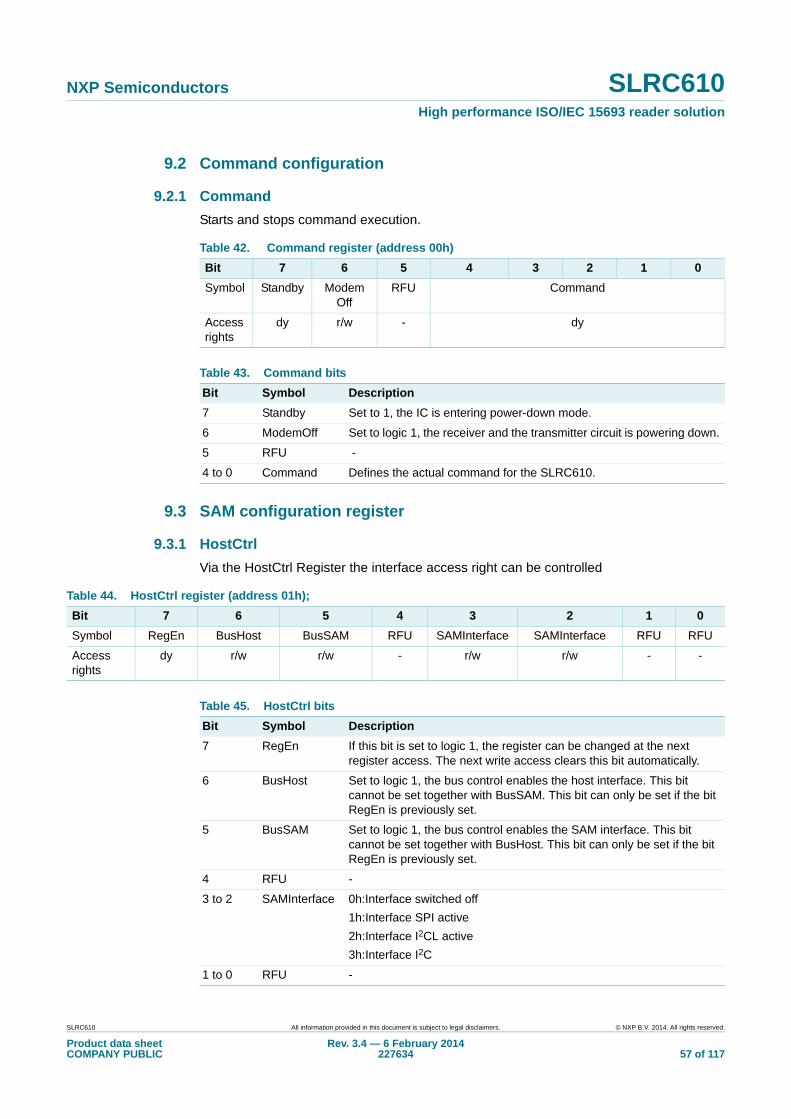
NXP Semiconductors SLRC610High performance ISO/IEC 15693 reader solution
9.2 Command configuration
9.2.1 Command
Starts and stops command execution.
9.3 SAM configuration register
9.3.1 HostCtrl
Via the HostCtrl Register the interface access right can be controlled
Table 42. Command register (address 00h)
Bit 7 6 5 4 3 2 1 0
Symbol Standby Modem Off
RFU Command
Access rights
dy r/w - dy
Table 43. Command bits
Bit Symbol Description
7 Standby Set to 1, the IC is entering power-down mode.
6 ModemOff Set to logic 1, the receiver and the transmitter circuit is powering down.
5 RFU -
4 to 0 Command Defines the actual command for the SLRC610.
Table 44. HostCtrl register (address 01h);
Bit 7 6 5 4 3 2 1 0
Symbol RegEn BusHost BusSAM RFU SAMInterface SAMInterface RFU RFU
Access rights
dy r/w r/w - r/w r/w - -
Table 45. HostCtrl bits
Bit Symbol Description
7 RegEn If this bit is set to logic 1, the register can be changed at the next register access. The next write access clears this bit automatically.
6 BusHost Set to logic 1, the bus control enables the host interface. This bit cannot be set together with BusSAM. This bit can only be set if the bit RegEn is previously set.
5 BusSAM Set to logic 1, the bus control enables the SAM interface. This bit cannot be set together with BusHost. This bit can only be set if the bit RegEn is previously set.
4 RFU -
3 to 2 SAMInterface 0h:Interface switched off
1h:Interface SPI active
2h:Interface I2CL active
3h:Interface I2C
1 to 0 RFU -
SLRC610 All information provided in this document is subject to legal disclaimers. © NXP B.V. 2014. All rights reserved.
Product data sheetCOMPANY PUBLIC
Rev. 3.4 — 6 February 2014227634 57 of 117

NXP Semiconductors SLRC610High performance ISO/IEC 15693 reader solution
9.4 FIFO configuration register
9.4.1 FIFOControl
FIFOControl defines the characteristics of the FIFO
9.4.2 WaterLevel
Defines the level for FIFO under- and overflow warning levels.This register is extended by 1 bit in FIFOControl in case the 512-byte FIFO mode is activated by setting bit FIFOControl.FIFOSize.
Table 46. FIFOControl register (address 02h);
Bit 7 6 5 4 3 2 1 0
Symbol FIFOSize HiAlert LoAlert FIFOFlush RFU WaterLevel FIFOLength
Access rights
r/w r r w - r/w r
Table 47. FIFOControl bits
Bit Symbol Description
7 FIFOSize Set to logic 1, FIFO size is 255 bytes; Set to logic 0, FIFO size is 512 bytes. It is recommended to change the FIFO size only, when the FIFO content had been cleared.
6 HiAlert Set to logic 1, when the number of bytes stored in the FIFO buffer fulfils the following equation:
HiAlert = (FIFOSize - FIFOLength) <= WaterLevel
5 LoAlert Set to logic 1, when the number of bytes stored in the FIFO buffer fulfils the following conditions:
LoAlert =1 if FIFOLength <= WaterLevel
4 FIFOFlush Set to logic 1 empties the FIFO buffer. Reading this bit will always return 0
3 RFU -
2 WaterLevel Defines the bit 8 (MSB) for the waterlevel (extension of WaterLevel). This bit is only evaluated in the 512-byte FIFO mode. Bits 7..0 are defined in WaterLevel.
1 to 0 FIFOLength Defines the bit9 (MSB) and bit8 for the FIFO length (extension of FIFOLength). These two bits are only evaluated in the 512-byte FIFO mode, The bits 7..0 are defined in FIFOLength.
Table 48. WaterLevel register (address 03h);
Bit 7 6 5 4 3 2 1 0
Symbol WaterLevel
Access rights
r/w
SLRC610 All information provided in this document is subject to legal disclaimers. © NXP B.V. 2014. All rights reserved.
Product data sheetCOMPANY PUBLIC
Rev. 3.4 — 6 February 2014227634 58 of 117

NXP Semiconductors SLRC610High performance ISO/IEC 15693 reader solution
Table 49. WaterLevel bits
Bit Symbol Description
7 to 0 WaterLevel Sets a level to indicate a FIFO-buffer state which can be read from bits HighAlert and LowAlert in the FifoControl. In 512-byte FIFO mode, the register is extended by bit WaterLevel in the FIFOControl. This functionality can be used to avoid a FIFO buffer overflow or underflow:
The bit HiAlert bit in FIFO Control is read logic 1, if the number of bytes in the FIFO-buffer is equal or less than the number defined by WaterLevel.
The bit LoAlert bit in FIFO control is read logic 1, if the number of bytes in the FIFO buffer is equal or less than the number defined by WaterLevel.
Note: For the calculation of HiAlert and LoAlert see register description of these bits (Section 9.4.1 “FIFOControl”).
SLRC610 All information provided in this document is subject to legal disclaimers. © NXP B.V. 2014. All rights reserved.
Product data sheetCOMPANY PUBLIC
Rev. 3.4 — 6 February 2014227634 59 of 117

NXP Semiconductors SLRC610High performance ISO/IEC 15693 reader solution
9.4.3 FIFOLength
Number of bytes in the FIFO buffer. In 512-byte mode this register is extended by FIFOControl.FifoLength.
9.4.4 FIFOData
In- and output of FIFO buffer. Contrary to any read/write access to other addresses, reading or writing to the FIFO address does not increment the address pointer. Resulting in an efficient data transfer from and to the FIFO buffer. Writing to the FIFOData register increments, reading decrements the number of bytes present in the FIFO.
9.5 Interrupt configuration registers
The Registers IRQ0 register and IRQ1 register implement a special functionality to avoid the not intended modification of bits.
The mechanism of changing register contents requires the following consideration: IRQ(x). Set indicates, if a set bit on position 0 to 6 shall be cleared or set. Depending on the content of IRQ(x).Set, a write of a logical 1 to positions 0 to 6 either clears or sets the corresponding bit. With this register the application can modify the interrupt status which is maintained by the SLRC610.
Bit 7 indicates, if the intended modification is a setting or clearance of a bit. Any 1 written to a bit position 6...0 will trigger the setting or clearance of this bit as defined by bit 7. Example: writing FFh sets all bits 6..0, writing 7Fh clears all bits 6..0 of the interrupt request register
Table 50. FIFOLength register (address 04h); reset value: 00h
Bit 7 6 5 4 3 2 1 0
Symbol FIFOLength
Access rights
dy
Table 51. FIFOLength bits
Bit Symbol Description
7 to 0 FIFOLength Indicates the number of bytes in the FIFO buffer. In 512-byte mode this register is extended by the bits FIFOLength in the FIFOControl register. Writing to the FIFOData register increments, reading decrements the number of available bytes in the FIFO.
Table 52. FIFOData register (address 05h);
Bit 7 6 5 4 3 2 1 0
Symbol FIFOData
Access rights
dy
Table 53. FIFOData bits
Bit Symbol Description
7 to 0 FIFOData Data input and output port for the internal FIFO buffer. Refer to Section 8.5 “Buffer”.
SLRC610 All information provided in this document is subject to legal disclaimers. © NXP B.V. 2014. All rights reserved.
Product data sheetCOMPANY PUBLIC
Rev. 3.4 — 6 February 2014227634 60 of 117

NXP Semiconductors SLRC610High performance ISO/IEC 15693 reader solution
9.5.1 IRQ0 register
Interrupt request register 0.
9.5.2 IRQ1 register
Interrupt request register 1.
Table 54. IRQ0 register (address 06h); reset value: 00h
Bit 7 6 5 4 3 2 1 0
Symbol Set Hi AlertIrq Lo AlertIrq IdleIrq TxIrq RxIrq ErrIrq RxSOFIrq
Access rights
w dy dy dy dy dy dy dy
Table 55. IRQ0 bits
Bit Symbol Description
7 Set 1: writing a 1 to a bit position 6..0 sets the interrupt request
0: Writing a 1 to a bit position 6..0 clears the interrupt request
6 HiAlerIrq Set, when bit HiAlert in register Status1Reg is set. In opposition to HiAlert, HiAlertIrq stores this event and can only be reset if Set is cleared.
5 LoAlertIrq Set, when bit LoAlert in register Status1 is set. In opposition to LoAlert, LoAlertIrq stores this event and can only be reset if Set is cleared
4 IdleIrq Set, when a command terminates by itself e.g. when the Command changes its value from any command to the Idle command. If an unknown command is started, the Command changes its content to the idle state and the bit IdleIRq is set. Starting the Idle command by the Controller does not set bit IdleIRq. Can only be reset if Set is cleared.
3 TxIrq Set, when data transmission is completed, which is immediately after the last bit is sent. Can only be reset if Set is cleared.
2 RxIrq Set, when the receiver detects the end of a data stream.
Note: This flag is no indication that the received data stream is correct. The error flags have to be evaluated to get the status of the reception. Can only be reset if Set is cleared.
1 ErrIrq Set, when the one of the following errors is set:
FifoWrErr, FiFoOvl, ProtErr, NoDataErr, IntegErr.
Can only be reset if Set is cleared.
0 RxSOFlrq Set, when a SOF or a subcarrier is detected. Can only be reset if Set is cleared.
Table 56. IRQ1 register (address 07h)
Bit 7 6 5 4 3 2 1 0
Symbol Set GlobalIrq LPCD_Irq Timer4Irq Timer3Irq Timer2Irq Timer1Irq Timer0Irq
Access rights
w dy dy dy dy dy dy dy
SLRC610 All information provided in this document is subject to legal disclaimers. © NXP B.V. 2014. All rights reserved.
Product data sheetCOMPANY PUBLIC
Rev. 3.4 — 6 February 2014227634 61 of 117

NXP Semiconductors SLRC610High performance ISO/IEC 15693 reader solution
9.5.3 IRQ0En register
Interrupt request enable register for IRQ0. This register allows to define if an interrupt request is processed by the SLRC610.
9.5.4 IRQ1En
Interrupt request enable register for IRQ1.
Table 57. IRQ1 bits
Bit Symbol Description
7 Set 1: writing a 1 to a bit position 5..0 sets the interrupt request
0: Writing a 1 to a bit position 5..0 clears the interrupt request
6 GlobalIrq Set, if an enabled Irq occurs.
5 LPCD_Irq Set if a card is detected in Low-power card detection sequence.
4 Timer4Irq Set to logic 1 when Timer4 has an underflow.
3 Timer3Irq Set to logic 1 when Timer3 has an underflow.
2 Timer2Irq Set to logic 1 when Timer2 has an underflow.
1 Timer1Irq Set to logic 1 when Timer1 has an underflow.
0 Timer0Irq Set to logic 1 when Timer0 has an underflow.
Table 58. IRQ0En register (address 08h)
Bit 7 6 5 4 3 2 1 0
Symbol Irq_Inv Hi AlertIrqEn LoAlertIrqEn IdleIrqEn TxIrqEn RxIrqEn ErrIrqEn RxSOFIrqEn
Access rights
r/w r/w r/w r/w r/w r/w r/w r/w
Table 59. IRQ0En bits
Bit Symbol Description
7 Irq_Inv Set to one the signal of the IRQ pin is inverted
6 Hi AlerIrqEn Set to logic 1, it allows the High Alert interrupt Request (indicated by the bit HiAlertIrq) to be propagated to the GlobalIrq
5 Lo AlertIrqEn Set to logic 1, it allows the Low Alert Interrupt Request (indicated by the bit LoAlertIrq) to be propagated to the GlobalIrq
4 IdleIrqEn Set to logic 1, it allows the Idle interrupt request (indicated by the bit IdleIrq) to be propagated to the GlobalIrq
3 TxIRqEn Set to logic 1, it allows the transmitter interrupt request (indicated by the bit TxtIrq) to be propagated to the GlobalIrq
2 RxIRqEn Set to logic 1, it allows the receiver interrupt request (indicated by the bit RxIrq) to be propagated to the GlobalIrq
1 ErrIRqEn Set to logic 1, it allows the Error interrupt request (indicated by the bit ErrorIrq) to be propagated to the GlobalIrq
0 RxSOFIrqEn Set to logic 1, it allows the RxSOF interrupt request (indicated by the bit RxSOFIrq) to be propagated to the GlobalIrq
SLRC610 All information provided in this document is subject to legal disclaimers. © NXP B.V. 2014. All rights reserved.
Product data sheetCOMPANY PUBLIC
Rev. 3.4 — 6 February 2014227634 62 of 117

NXP Semiconductors SLRC610High performance ISO/IEC 15693 reader solution
9.6 Contactless interface configuration registers
9.6.1 Error
Error register.
Table 60. IRQ1EN register (address 09h);
Bit 7 6 5 4 3 2 1 0
Symbol IrqPushPull IrqPinEn LPCD_IrqEn Timer4IrqEn Timer3IrqEn Timer2IrqEn
Timer1IrqEn Timer0IrqEn
Access rights
r/w r/w r/w r/w r/w r/w r/w r/w
Table 61. IRQ1EN bits
Bit Symbol Description
7 IrqPushPull Set to 1 the IRQ-pin acts as PushPull pin, otherwise it acts as OpenDrain pin
6 IrqPinEN Set to logic 1, it allows the global interrupt request (indicated by the bit GlobalIrq) to be propagated to the interrupt pin
5 LPCD_IrqEN Set to logic 1, it allows the LPCDinterrupt request (indicated by the bit LPCDIrq) to be propagated to the GlobalIrq
4 Timer4IRqEn Set to logic 1, it allows the Timer4 interrupt request (indicated by the bit Timer4Irq) to be propagated to the GlobalIrq
3 Timer3IrqEn Set to logic 1, it allows the Timer3 interrupt request (indicated by the bit Timer3tIrq) to be propagated to the GlobalIrq
2 Timer2IrqEn Set to logic 1, it allows the Timer2 interrupt request (indicated by the bit Timer2Irq) to be propagated to the GlobalIrq
1 Timer1IrqEn Set to logic 1, it allows the Timer1 interrupt request (indicated by the bit Timer1Irq) to be propagated to the GlobalIrq
0 Timer0IrqEn Set to logic 1, it allows the Timer0 interrupt request (indicated by the bit Timer0Irq) to be propagated to the GlobalIrq
Table 62. Error register (address 0Ah)
Bit 7 6 5 4 3 2 1 0
Symbol EE_Err FiFoWrErr FIFOOvl MinFrameErr NoDataErr CollDet ProtErr IntegErr
Access rights
dy dy dy dy dy dy dy dy
SLRC610 All information provided in this document is subject to legal disclaimers. © NXP B.V. 2014. All rights reserved.
Product data sheetCOMPANY PUBLIC
Rev. 3.4 — 6 February 2014227634 63 of 117

NXP Semiconductors SLRC610High performance ISO/IEC 15693 reader solution
9.6.2 Status
Status register.
Table 63. Error bits
Bit Symbol Description
7 EE_Err An error appeared during the last EEPROM command. For
details see the descriptions of the EEPROM commands
6 FIFOWrErr Data was written into the FIFO, during a transmission of a possible CRC, during "RxWait", "Wait for data" or "Receiving" state, or during an authentication command. The Flag is cleared when a new CL command is started. If RxMultiple is active, the flag is cleared after the error flags have been written to the FIFO.
5 FIFOOvl Data is written into the FIFO when it is already full. The data that is already in the FIFO will remain untouched. All data that is written to the FIFO after this Flag is set to 1 will be ignored.
4 MinFrameErr
A valid SOF was received, but afterwards less then 4 bits of data were received.
Note: Frames with less than 4 bits of data are automatically discarded and the RxDecoder stays enabled. Furthermore no RxIrq is set. The same is valid for less than 3 Bytes if the EMD suppression is activated
Note: MinFrameErr is automatically cleared at the start of a receive or transceive command. In case of a transceive command, it is cleared at the start of the receiving phase ("Wait for data" state)
3 NoDataErr Data should be sent, but no data is in FIFO
2 CollDet A collision has occurred. The position of the first collision is shown in the register RxColl.
Note: CollDet is automatically cleared at the start of a receive or transceive command. In case of a transceive command, it is cleared at the start of the receiving phase (“Wait for data” state).
Note: If a collision is part of the defined EOF symbol, CollDet is not set to 1.
1 ProtErr A protocol error has occurred. A protocol error can be a wrong stop bit or SOF or a wrong number of received data bytes. When a protocol error is detected, data reception is stopped.
Note: ProtErr is automatically cleared at start of a receive or transceive command. In case of a transceive command, it is cleared at the start of the receiving phase (“Wait for data” state).
Note: When a protocol error occurs the last received data byte is not written into the FIFO.
0 IntegErr A data integrity error has been detected. Possible cause can be a wrong parity or a wrong CRC. In case of a data integrity error the reception is continued.
Note: IntegErr is automatically cleared at start of a Receive or Transceive command. In case of a Transceive command, it is cleared at the start of the receiving phase (“Wait for data” state).
Note: If the NoColl bit is set, also a collision is setting the IntegErr.
SLRC610 All information provided in this document is subject to legal disclaimers. © NXP B.V. 2014. All rights reserved.
Product data sheetCOMPANY PUBLIC
Rev. 3.4 — 6 February 2014227634 64 of 117

NXP Semiconductors SLRC610High performance ISO/IEC 15693 reader solution
9.6.3 RxBitCtrl
Receiver control register.
Table 64. Status register (address 0Bh)
Bit 7 6 5 4 3 2 1 0
Symbol - - - - - ComState
Access rights
RFU RFU RFU RFU RFU r
Table 65. Status bits
Bit Symbol Description
7 to 3 - RFU
2 to 0 ComState ComState shows the status of the transmitter and receiver state machine:
000b ... Idle
001b ... TxWait
011b ... Transmitting
101b ... RxWait
110b ... Wait for data
111b ... Receiving
100b ... not used
Table 66. RxBitCtrl register (address 0Ch);
Bit 7 6 5 4 3 2 1 0
Symbol ValuesAfterColl RxAlign NoColl RxLastBits
Access rights
r/w r/w r/w w
Table 67. RxBitCtrl bits
Bit Symbol Description
7 ValuesAfter Coll
If cleared, every received bit after a collision is replaced by a zero. This function is needed for ISO/IEC14443 anticollision
SLRC610 All information provided in this document is subject to legal disclaimers. © NXP B.V. 2014. All rights reserved.
Product data sheetCOMPANY PUBLIC
Rev. 3.4 — 6 February 2014227634 65 of 117

NXP Semiconductors SLRC610High performance ISO/IEC 15693 reader solution
6 to 4 RxAlign Used for reception of bit oriented frames: RxAlign defines the bit position length for the first bit received to be stored. Further received bits are stored at the following bit positions.
Example:
RxAlign = 0h - the LSB of the received bit is stored at bit 0, the second received bit is stored at bit position 1.
RxAlign = 1h - the LSB of the received bit is stored at bit 1, the second received bit is stored at bit position 2.
RxAlign = 7h - the LSB of the received bit is stored at bit 7, the second received bit is stored in the following byte at position 0.
Note: If RxAlign = 0, data is received byte-oriented, otherwise bit-oriented.
3 NoColl If this bit is set, a collision will result in an IntegErr
2 to 0 RxLastBits Defines the number of valid bits of the last data byte received in bit-oriented communications. If zero the whole byte is valid.
Note: These bits are set by the RxDecoder in a bit-oriented communication at the end of the communication. They are reset at start of reception.
Table 67. RxBitCtrl bits
Bit Symbol Description
SLRC610 All information provided in this document is subject to legal disclaimers. © NXP B.V. 2014. All rights reserved.
Product data sheetCOMPANY PUBLIC
Rev. 3.4 — 6 February 2014227634 66 of 117

NXP Semiconductors SLRC610High performance ISO/IEC 15693 reader solution
9.6.4 RxColl
Receiver collision register.
Table 68. RxColl register (address 0Dh);
Bit 7 6 5 4 3 2 1 0
Symbol CollPosValid CollPos
Access rights
r r
Table 69. RxColl bits
Bit Symbol Description
7 CollPosValid
If set to 1, the value of CollPos is valid. Otherwise no collision is detected or the position of the collision is out of the range of bits CollPos.
6 to 0 CollPos These bits show the bit position of the first detected collision in a received frame (only data bits are interpreted). CollPos can only be displayed for the first 8 bytes of a data stream.
Example:
00h indicates a bit collision in the 1st bit
01h indicates a bit collision in the 2nd bit
08h indicates a bit collision in the 9th bit (1st bit of 2nd byte)
3Fh indicates a bit collision in the 64th bit (8th bit of the 8th byte)
These bits shall only be interpreted in ISO/IEC 15693/ICODE SLI read/write mode if bit CollPosValid is set.
Note: If RxBitCtrl.RxAlign is set to a value different to 0, this value is included in the CollPos.
Example: RxAlign = 4h, a collision occurs in the 4th received bit (which is the last bit of that UID byte). The CollPos = 7h in this case.
SLRC610 All information provided in this document is subject to legal disclaimers. © NXP B.V. 2014. All rights reserved.
Product data sheetCOMPANY PUBLIC
Rev. 3.4 — 6 February 2014227634 67 of 117

NXP Semiconductors SLRC610High performance ISO/IEC 15693 reader solution
9.7 Timer configuration registers
9.7.1 TControl
Control register of the timer section.
The TControl implements a special functionality to avoid the not intended modification of bits.
Bit 3..0 indicates, which bits in the positions 7..4 are intended to be modified.
Example: writing FFh sets all bits 7..4, writing F0h does not change any of the bits 7..4
9.7.2 T0Control
Control register of the Timer0.
Table 70. TControl register (address 0Eh)
Bit 7 6 5 4 3 2 1 0
Symbol T3Running T2Running T1Running T0Running T3StartStopNow
T2StartStopNow
T1StartStopNow
T0StartStopNow
Access rights
dy dy dy dy w w w w
Table 71. TControl bits
Bit Symbol Description
7 T3Running Indicates Timer3 is running.If the bit T3startStopNow is set/reset, this bit and the timer can be started/stopped
6 T2Running Indicates Timer2 is running. If the bit T2startStopNow is set/reset, this bit and the timer can be started/stopped
5 T1Running Indicates tTmer1 is running. If the bit T1startStopNow is set/reset, this bit and the timer can be started/stopped
4 T0Running Indicates Timer0 is running. If the bit T0startStopNow is set/reset, this bit and the timer can be started/stopped
3 T3StartStopNow
The bit 7 of TControl T3Running can be modified if set
2 T2StartStopNow
The bit 6of TControl T2Running can be modified if set
1 T1StartStopNow
The bit 5of TControl T1Running can be modified if set
0 T0StartStopNow
The bit 4 of TControl T0Running can be modified if set
Table 72. T0Control register (address 0Fh);
Bit 7 6 5 4 3 2 1 0
Symbol T0StopRx - T0Start T0AutoRestart - T0Clk
Access rights
r/w RFU r/w r/w RFU r/w
SLRC610 All information provided in this document is subject to legal disclaimers. © NXP B.V. 2014. All rights reserved.
Product data sheetCOMPANY PUBLIC
Rev. 3.4 — 6 February 2014227634 68 of 117

NXP Semiconductors SLRC610High performance ISO/IEC 15693 reader solution
9.7.2.1 T0ReloadHi
High byte reload value of the Timer0.
9.7.2.2 T0ReloadLo
Low byte reload value of the Timer0.
Table 73. T0Control bits
Bit Symbol Description
7 T0StopRx If set, the timer stops immediately after receiving the first 4 bits. If cleared the timer does not stop automatically.
Note: If LFO Trimming is selected by T0Start, this bit has no effect.
6 - RFU
5 to 4 T0Start 00b: The timer is not started automatically
01b: The timer starts automatically at the end of the transmission
10b: Timer is used for LFO trimming without underflow (Start/Stop on PosEdge)
11b: Timer is used for LFO trimming with underflow (Start/Stop on PosEdge)
3 T0AutoRestart 1: the timer automatically restarts its count-down from T0ReloadValue, after the counter value has reached the value zero.
0: the timer decrements to zero and stops.
The bit Timer1Irq is set to logic 1 when the timer underflows.
2 - RFU
1 to 0 T0Clk 00b: The timer input clock is 13.56 MHz.
01b: The timer input clock is 211,875 kHz.
10b: The timer input clock is an underflow of Timer2.
11b: The timer input clock is an underflow of Timer1.
Table 74. T0ReloadHi register (address 10h);
Bit 7 6 5 4 3 2 1 0
Symbol T0Reload Hi
Access rights
r/w
Table 75. T0ReloadHi bits
Bit Symbol Description
7 to 0 T0ReloadHi Defines the high byte of the reload value of the timer. With the start event the timer loads the value of the registers T0ReloadValHi, T0ReloadValLo. Changing this register affects the timer only at the next start event.
Table 76. T0ReloadLo register (address 11h);
Bit 7 6 5 4 3 2 1 0
Symbol T0ReloadLo
Access rights
r/w
SLRC610 All information provided in this document is subject to legal disclaimers. © NXP B.V. 2014. All rights reserved.
Product data sheetCOMPANY PUBLIC
Rev. 3.4 — 6 February 2014227634 69 of 117

NXP Semiconductors SLRC610High performance ISO/IEC 15693 reader solution
9.7.2.3 T0CounterValHi
High byte of the counter value of Timer0.
9.7.2.4 T0CounterValLo
Low byte of the counter value of Timer0.
9.7.2.5 T1Control
Control register of the Timer1.
Table 77. T0ReloadLo bits
Bit Symbol Description
7 to0 T0ReloadLo Defines the low byte of the reload value of the timer. With the start event the timer loads the value of the T0ReloadValHi, T0ReloadValLo. Changing this register affects the timer only at the next start event.
Table 78. T0CounterValHi register (address 12h)
Bit 7 6 5 4 3 2 1 0
Symbol T0CounterValHi
Access rights
dy
Table 79. T0CounterValHi bits
Bit Symbol Description
7to0 T0CounterValHi
High byte value of the Timer0. This value shall not be read out during reception.
Table 80. T0CounterValLo register (address 13h)
Bit 7 6 5 4 3 2 1 0
Symbol T0CounterValLo
Access rights
dy
Table 81. T0CounterValLo bits
Bit Symbol Description
7 to 0 T0CounterValLo Low byte value of the Timer0.This value shall not be read out during reception.
Table 82. T1Control register (address 14h);
Bit 7 6 5 4 3 2 1 0
Symbol T1StopRx - T1Start T1AutoRestart - T1Clk
Access rights
r/w RFU r/w r/w RFU r/w
SLRC610 All information provided in this document is subject to legal disclaimers. © NXP B.V. 2014. All rights reserved.
Product data sheetCOMPANY PUBLIC
Rev. 3.4 — 6 February 2014227634 70 of 117

NXP Semiconductors SLRC610High performance ISO/IEC 15693 reader solution
9.7.2.6 T1ReloadHi
High byte (MSB) reload value of the Timer1.
9.7.2.7 T1ReloadLo
Low byte (LSB) reload value of the Timer1.
Table 83. T1Control bits
Bit Symbol Description
7 T1StopRx If set, the timer stops after receiving the first 4 bits. If cleared, the timer is not stopped automatically.
Note: If LFO trimming is selected by T1start, this bit has no effect.
6 - RFU
5 to 4 T1Start 00b: The timer is not started automatically
01b: The timer starts automatically at the end of the transmission
10b: Timer is used for LFO trimming without underflow (Start/Stop on PosEdge)
11b: Timer is used for LFO trimming with underflow (Start/Stop on PosEdge)
3 T1AutoRestart Set to logic 1, the timer automatically restarts its countdown from T1ReloadValue, after the counter value has reached the value zero.
Set to logic 0 the timer decrements to zero and stops.
The bit Timer1IRq is set to logic 1 when the timer underflows.
2 - RFU
1 to 0 T1Clk 00b: The timer input clock is 13.56 MHz
01b: The timer input clock is 211,875 kHz.
10b: The timer input clock is an underflow of Timer0
11b: The timer input clock is an underflow of Timer2
Table 84. T0ReloadHi register (address 15h)
Bit 7 6 5 4 3 2 1 0
Symbol T1ReloadHi
Access rights
r/w
Table 85. T1ReloadHi bits
Bit Symbol Description
7 to 0 T1ReloadHi Defines the high byte reload value of the Timer 1. With the start event the timer loads the value of the T1ReloadValHi and T1ReloadValLo. Changing this register affects the Timer only at the next start event.
Table 86. T1ReloadLo register (address 16h)
Bit 7 6 5 4 3 2 1 0
Symbol T1ReloadLo
Access rights
r/w
SLRC610 All information provided in this document is subject to legal disclaimers. © NXP B.V. 2014. All rights reserved.
Product data sheetCOMPANY PUBLIC
Rev. 3.4 — 6 February 2014227634 71 of 117

NXP Semiconductors SLRC610High performance ISO/IEC 15693 reader solution
9.7.2.8 T1CounterValHi
High byte (MSB) of the counter value of byte Timer1.
9.7.2.9 T1CounterValLo
Low byte (LSB) of the counter value of byte Timer1.
9.7.2.10 T2Control
Control register of the Timer2.
Table 87. T1ReloadValLo bits
Bit Symbol Description
7 to 0 T1ReloadLo Defines the low byte of the reload value of the Timer1. Changing this register affects the timer only at the next start event.
Table 88. T1CounterValHi register (address 17h)
Bit 7 6 5 4 3 2 1 0
Symbol T1CounterValHi
Access rights
dy
Table 89. T1CounterValHi bits
Bit Symbol Description
7 to 0 T1CounterValHi
High byte of the current value of the Timer1. This value shall not be read out during reception.
Table 90. T1CounterValLo register (address 18h)
Bit 7 6 5 4 3 2 1 0
Symbol T1CounterValLo
Access rights
dy
Table 91. T1CounterValLo bits
Bit Symbol Description
7 to 0 T1CounterValLo
Low byte of the current value of the counter 1. This value shall not be read out during reception.
Table 92. T2Control register (address 19h)
Bit 7 6 5 4 3 2 1 0
Symbol T2StopRx - T2Start T2AutoRestart - T2Clk
Access rights
r/w RFU r/w r/w RFU r/w
SLRC610 All information provided in this document is subject to legal disclaimers. © NXP B.V. 2014. All rights reserved.
Product data sheetCOMPANY PUBLIC
Rev. 3.4 — 6 February 2014227634 72 of 117

NXP Semiconductors SLRC610High performance ISO/IEC 15693 reader solution
9.7.2.11 T2ReloadHi
High byte of the reload value of Timer2.
9.7.2.12 T2ReloadLo
Low byte of the reload value of Timer2.
Table 93. T2Control bits
Bit Symbol Description
7 T2StopRx If set the timer stops immediately after receiving the first 4 bits. If cleared indicates, that the timer is not stopped automatically.Note: If LFO Trimming is selected by T2Start, this bit has no effect.
6 - RFU
5 to 4 T2Start 00b: The timer is not started automatically.
01b: The timer starts automatically at the end of the transmission.
10b: Timer is used for LFO trimming without underflow (Start/Stop on PosEdge).
11b: Timer is used for LFO trimming with underflow (Start/Stop on PosEdge).
3 T2AutoRestart Set to logic 1, the timer automatically restarts its countdown from T2ReloadValue, after the counter value has reached the value zero. Set to logic 0 the timer decrements to zero and stops. The bit Timer2IRq is set to logic 1 when the timer underflows
2 - RFU
1 to 0 T2Clk 00b: The timer input clock is 13.56 MHz.
01b: The timer input clock is 212 kHz.
10b: The timer input clock is an underflow of Timer0
11b: The timer input clock is an underflow of Timer1
Table 94. T2ReloadHi register (address 1Ah)
Bit 7 6 5 4 3 2 1 0
Symbol T2ReloadHi
Access rights
r/w
Table 95. T2Reload bits
Bit Symbol Description
7 to 0 T2ReloadHi Defines the high byte of the reload value of the Timer2. With the start event the timer load the value of the T2ReloadValHi and T2ReloadValLo. Changing this register affects the timer only at the next start event.
Table 96. T2ReloadLo register (address 1Bh)
Bit 7 6 5 4 3 2 1 0
Symbol T2ReloadLo
Access rights
r/w
SLRC610 All information provided in this document is subject to legal disclaimers. © NXP B.V. 2014. All rights reserved.
Product data sheetCOMPANY PUBLIC
Rev. 3.4 — 6 February 2014227634 73 of 117

NXP Semiconductors SLRC610High performance ISO/IEC 15693 reader solution
9.7.2.13 T2CounterValHi
High byte of the counter register of Timer2.
9.7.2.14 T2CounterValLoReg
Low byte of the current value of Timer 2.
9.7.2.15 T3Control
Control register of the Timer 3.
Table 97. T2ReloadLo bits
Bit Symbol Description
7 to 0 T2ReloadLo Defines the low byte of the reload value of the Timer2. With the start event the timer load the value of the T2ReloadValHi and T2RelaodVaLo. Changing this register affects the timer only at the next start event.
Table 98. T2CounterValHi register (address 1Ch)
Bit 7 6 5 4 3 2 1 0
Symbol T2CounterValHi
Access rights
dy
Table 99. T2CounterValHi bits
Bit Symbol Description
7 to 0 T2CounterValHi
High byte current counter value of Timer2. This value shall not be read out during reception.
Table 100. T2CounterValLo register (address 1Dh)
Bit 7 6 5 4 3 2 1 0
Symbol T2CounterValLo
Access rights
dy
Table 101. T2CounterValLo bits
Bit Symbol Description
7 to 0 T2CounterValLo
Low byte of the current counter value of Timer1Timer2. This value shall not be read out during reception.
Table 102. T3Control register (address 1Eh)
Bit 7 6 5 4 3 2 1 0
Symbol T3StopRx - T3Start T3AutoRestart - T3Clk
Access rights
r/w RFU r/w r/w RFU r/w
SLRC610 All information provided in this document is subject to legal disclaimers. © NXP B.V. 2014. All rights reserved.
Product data sheetCOMPANY PUBLIC
Rev. 3.4 — 6 February 2014227634 74 of 117

NXP Semiconductors SLRC610High performance ISO/IEC 15693 reader solution
9.7.2.16 T3ReloadHi
High byte of the reload value of Timer3.
9.7.2.17 T3ReloadLo
Low byte of the reload value of Timer3.
Table 103. T3Control bits
Bit Symbol Description
7 T3StopRx If set, the timer stops immediately after receiving the first 4 bits. If cleared, indicates that the timer is not stopped automatically.
Note: If LFO Trimming is selected by T3Start, this bit has no effect.
6 - RFU
5 to 4 T3Start 00b - timer is not started automatically
01b - timer starts automatically at the end of the transmission
10b - timer is used for LFO trimming without underflow (Start/Stop on PosEdge)
11b - timer is used for LFO trimming with underflow (Start/Stop on PosEdge).
3 T3AutoRestart Set to logic 1, the timer automatically restarts its countdown from T3ReloadValue, after the counter value has reached the value zero.
Set to logic 0 the timer decrements to zero and stops.
The bit Timer1IRq is set to logic 1 when the timer underflows.
2 - RFU
1 to 0 T3Clk 00b - the timer input clock is 13.56 MHz.
01b - the timer input clock is 211,875 kHz.
10b - the timer input clock is an underflow of Timer0
11b - the timer input clock is an underflow of Timer1
Table 104. T3ReloadHi register (address 1Fh);
Bit 7 6 5 4 3 2 1 0
Symbol T3ReloadHi
Access rights
r/w
Table 105. T3ReloadHi bits
Bit Symbol Description
7 to 0 T3ReloadHi Defines the high byte of the reload value of the Timer3. With the start event the timer load the value of the T3ReloadValHi and T3ReloadValLo. Changing this register affects the timer only at the next start event.
Table 106. T3ReloadLo register (address 20h)
Bit 7 6 5 4 3 2 1 0
Symbol T3ReloadLo
Access rights
r/w
SLRC610 All information provided in this document is subject to legal disclaimers. © NXP B.V. 2014. All rights reserved.
Product data sheetCOMPANY PUBLIC
Rev. 3.4 — 6 February 2014227634 75 of 117

NXP Semiconductors SLRC610High performance ISO/IEC 15693 reader solution
9.7.2.18 T3CounterValHi
High byte of the current counter value the 16-bit Timer3.
9.7.2.19 T3CounterValLo
Low byte of the current counter value the 16-bit Timer3.
9.7.2.20 T4Control
The wake-up timer T4 activates the system after a given time. If enabled, it can start the low power card detection function.
Table 107. T3ReloadLo bits
Bit Symbol Description
7 to 0 T3ReloadLo Defines the low byte of the reload value of Timer3. With the start event the timer load the value of the T3ReloadValHi and T3RelaodValLo. Changing this register affects the timer only at the next start event.
Table 108. T3CounterValHi register (address 21h)
Bit 7 6 5 4 3 2 1 0
Symbol T3CounterValHi
Access rights
dy
Table 109. T3CounterValHi bits
Bit Symbol Description
7 to 0 T3CounterValHi
High byte of the current counter value of Timer3. This value shall not be read out during reception.
Table 110. T3CounterValLo register (address 22h)
Bit 7 6 5 4 3 2 1 0
Symbol T3CounterValLo
Access rights
dy
Table 111. T3CounterValLo bits
Bit Symbol Description
7 to 0 T3CounterValLo
Low byte current counter value of Timer3. This value shall not be read out during reception.
Table 112. T4Control register (address 23h)
Bit 7 6 5 4 3 2 1 0
Symbol T4Running T4StartStopNow
T4AutoTrimm
T4AutoLPCD
T4AutoRestart
T4AutoWakeUp T4Clk
Access rights
dy w r/w r/w r/w r/w r/w
SLRC610 All information provided in this document is subject to legal disclaimers. © NXP B.V. 2014. All rights reserved.
Product data sheetCOMPANY PUBLIC
Rev. 3.4 — 6 February 2014227634 76 of 117

NXP Semiconductors SLRC610High performance ISO/IEC 15693 reader solution
9.7.2.21 T4ReloadHi
High byte of the reload value of the 16-bit timer 4.
9.7.2.22 T4ReloadLo
Low byte of the reload value of the 16-bit timer 4.
Table 113. T4Control bits
Bit Symbol Description
7 T4Running Shows if the timer T4 is running. If the bit T4StartStopNow is set, this bit and the timer T4 can be started/stopped.
6 T4StartStopNow
if set, the bit T4Running can be changed.
5 T4AutoTrimm If set to one, the timer activates an LFO trimming procedure when it underflows. For the T4AutoTrimm function, at least one timer (T0 to T3) has to be configured properly for trimming (T3 is not allowed if T4AutoLPCD is set in parallel).
4 T4AutoLPCD If set to one, the timer activates a low-power card detection sequence. If a card is detected an interrupt request is raised and the system remains active if enabled. If no card is detected the SLRC610 enters the Power down mode if enabled. The timer is automatically restarted (no gap). Timer 3 is used to specify the time where the RF field is enabled to check if a card is present. Therefor you may not use Timer 3 for T4AutoTrimm in parallel.
3 T4AutoRestart Set to logic 1, the timer automatically restarts its countdown from T4ReloadValue, after the counter value has reached the value zero. Set to logic 0 the timer decrements to zero and stops. The bit Timer4Irq is set to logic 1 at timer underflow.
2 T4AutoWakeUp If set, the SLRC610 wakes up automatically, when the timer T4 has an underflow. This bit has to be set if the IC should enter the Power down mode after T4AutoTrimm and/or T4AutoLPCD is finished and no card has been detected. If the IC should stay active after one of these procedures this bit has to be set to 0.
1 to 0 T4Clk 00b - the timer input clock is the LFO clock01b - the timer input clock is the LFO clock/810b - the timer input clock is the LFO clock/1611b - the timer input clock is the LFO clock/32
Table 114. T4ReloadHi register (address 24h)
Bit 7 6 5 4 3 2 1 0
Symbol T4ReloadHi
Access rights
r/w
Table 115. T4ReloadHi bits
Bit Symbol Description
7 to 0 T4ReloadHi Defines high byte of the for the reload value of timer 4. With the start event the timer 4 loads the T4ReloadVal. Changing this register affects the timer only at the next start event.
SLRC610 All information provided in this document is subject to legal disclaimers. © NXP B.V. 2014. All rights reserved.
Product data sheetCOMPANY PUBLIC
Rev. 3.4 — 6 February 2014227634 77 of 117

NXP Semiconductors SLRC610High performance ISO/IEC 15693 reader solution
9.7.2.23 T4CounterValHi
High byte of the counter value of the 16-bit timer 4.
9.7.2.24 T4CounterValLo
Low byte of the counter value of the 16-bit timer 4.
9.8 Transmitter configuration registers
9.8.1 TxMode
Table 116. T4ReloadLo register (address 25h)
Bit 7 6 5 4 3 2 1 0
Symbol T4ReloadLo
Access rights
r/w
Table 117. T4ReloadLo bits
Bit Symbol Description
7 to 0 T4ReloadLo Defines the low byte of the reload value of the timer 4. With the start event the timer loads the value of the T4ReloadVal. Changing this register affects the timer only at the next start event.
Table 118. T4CounterValHi register (address 26h)
Bit 7 6 5 4 3 2 1 0
Symbol T4CounterValHi
Access rights
dy
Table 119. T4CounterValHi bits
Bit Symbol Description
7 to 0 T4CounterValHi High byte of the current counter value of timer 4.
Table 120. T4CounterValLo register (address 27h)
Bit 7 6 5 4 3 2 1 0
Symbol T4CounterValLo
Access rights
dy
Table 121. T4CounterValLo bits
Bit Symbol Description
7 to 0 T4CounterValLo Low byte of the current counter value of the timer 4.
Table 122. DrvMode register (address 28h)
Bit 7 6 5 4 3 2 1 0
Symbol Tx2Inv Tx1Inv - - TxEn TxClk Mode
Access rights
r/w r/w RFU RFU r/w r/w
SLRC610 All information provided in this document is subject to legal disclaimers. © NXP B.V. 2014. All rights reserved.
Product data sheetCOMPANY PUBLIC
Rev. 3.4 — 6 February 2014227634 78 of 117

NXP Semiconductors SLRC610High performance ISO/IEC 15693 reader solution
9.8.2 TxAmp
With the set_cw_amplitude register output power can be traded off against power supply rejection. Spending more headroom leads to better power supply rejection ration and better accuracy of the modulation degree.
With CwMax set, the voltage of TX1 will be pulled to the maximum possible. This register overrides the settings made by set_cw_amplitude.
9.8.3 TxCon
Table 123. DrvMode bits
Bit Symbol Description
7 Tx2Inv Inverts transmitter 2 at TX2 pin
6 Tx1Inv Inverts transmitter 1 at TX1 pin
5 RFU
4 - RFU
3 TxEn If set to 1 both transmitter pins are enabled
2 to 0 TxClkMode Transmitter clock settings (see 8.6.2. Table 27). Codes 011b and 0b110 are not supported. This register defines, if the output is operated in open drain, push-pull, at high impedance or pulled to a fix high or low level.
Table 124. TxAmp register (address 29h)
Bit 7 6 5 4 3 2 1 0
Symbol set_cw_amplitude - set_residual_carrier
Access rights
r/w RFU r/w
Table 125. TxAmp bits
Bit Symbol Description
7 to 6 set_cw_amplitude Allows to reduce the output amplitude of the transmitter by a fix value.
Four different preset values that are subtracted from TVDD can be selected:
0: TVDD -100 mV
1: TVDD -250 mV
2: TVDD -500 mV
3: TVDD -1000 mV
5 RFU -
4 to 0 set_residual_ carrier Set the residual carrier percentage. refer to Section 8.6.2
Table 126. TxCon register (address 2Ah)
Bit 7 6 5 4 3 2 1 0
Symbol OvershootT2 CwMax TxInv TxSel
Access rights
r/w r/w r/w r/w
SLRC610 All information provided in this document is subject to legal disclaimers. © NXP B.V. 2014. All rights reserved.
Product data sheetCOMPANY PUBLIC
Rev. 3.4 — 6 February 2014227634 79 of 117

NXP Semiconductors SLRC610High performance ISO/IEC 15693 reader solution
9.8.4 Txl
9.9 CRC configuration registers
9.9.1 TxCrcPreset
Table 127. TxCon bits
Bit Symbol Description
7 to 4 OvershootT2 Specifies the length (number of carrier clocks) of the additional modulation for overshoot prevention. Refer to Section 8.6.2.1 “Overshoot protection”
3 Cwmax Set amplitude of continuous wave carrier to the maximum.If set, set_cw_amplitude in Register TxAmp has no influence on the continuous amplitude.
2 TxInv If set, the resulting modulation signal defined by TxSel is inverted
1 to 0 TxSel Defines which signal is used as source for modulation00b ... no modulation 01b ... TxEnvelope 10b ... SigIn11b ... RFU
Table 128. Txl register (address 2Bh)
Bit 7 6 5 4 3 2 1 0
Symbol OvershootT1 tx_set_iLoad
Access rights
r/w r/w
Table 129. Txl bits
Bit Symbol Description
7 to 4 OvershootT1 Overshoot value for Timer1. Refer to Section 8.6.2.1 “Overshoot protection”
3 to 0 tx_set_iLoad Factory trim value, sets the expected Tx load current. This value is used to control the modulation index in an optimized way dependent on the expected TX load current.
Table 130. TXCrcPreset register (address 2Ch)
Bit 7 6 5 4 3 2 1 0
Symbol RFU TXPresetVal TxCRCtype TxCRCInvert TxCRCEn
Access rights
- r/w r/w r/w r/w
SLRC610 All information provided in this document is subject to legal disclaimers. © NXP B.V. 2014. All rights reserved.
Product data sheetCOMPANY PUBLIC
Rev. 3.4 — 6 February 2014227634 80 of 117

NXP Semiconductors SLRC610High performance ISO/IEC 15693 reader solution
Remark: User defined CRC preset values can be configured by EEprom (see Section 8.7.2.1, Table 29 “Configuration area (Page 0)”).
9.9.2 RxCrcCon
Table 131. TxCrcPreset bits
Bit Symbol Description
7 RFU -
6 to 4 TXPresetVal Specifies the CRC preset value for transmission (see Table 132).
3 to 2 TxCRCtype Defines which type of CRC (CRC8/CRC16/CRC5) is calculated:
• 00h -- CRC5
• 01h -- CRC8
• 02h -- CRC16
• 03h -- RFU
1 TxCRCInvert if set, the resulting CRC is inverted and attached to the data frame (ISO/IEC 3309)
0 TxCRCEn if set, a CRC is appended to the data stream
Table 132. Transmitter CRC preset value configuration
TXPresetVal[6...4] CRC16 CRC8 CRC5
0h 0000h 00h 00h
1h 6363h 12h 12h
2h A671h BFh -
3h FFFEh FDh -
4h - - -
5h - - -
6h User defined User defined User defined
7h FFFFh FFh 1Fh
Table 133. RxCrcCon register (address 2Dh)
Bit 7 6 5 4 3 2 1 0
Symbol RxForceCRCWrite RXPresetVal RXCRCtype RxCRCInvert RxCRCEn
Access rights
r/w r/w r/w r/w r/w
Table 134. RxCrcCon bits
Bit Symbol Description
7 RxForceCrcWrite
If set, the received CRC byte(s) are copied to the FIFO.
If cleared CRC Bytes are only checked, but not copied to the FIFO. This bit has to be always set in case of a not byte aligned CRC (e.g. ISO/IEC 18000-3 mode 3/ EPC Class-1HF)
6 to 4 RXPresetVal Defines the CRC preset value (Hex.) for transmission. (see Table 135).
SLRC610 All information provided in this document is subject to legal disclaimers. © NXP B.V. 2014. All rights reserved.
Product data sheetCOMPANY PUBLIC
Rev. 3.4 — 6 February 2014227634 81 of 117

NXP Semiconductors SLRC610High performance ISO/IEC 15693 reader solution
9.10 Transmitter configuration registers
9.10.1 TxDataNum
3 to 2 RxCRCtype Defines which type of CRC (CRC8/CRC16/CRC5) is calculated:
• 00h -- CRC5
• 01h -- CRC8
• 02h -- CRC16
• 03h -- RFU
1 RxCrcInvert If set, the CRC check is done for the inverted CRC.
0 RxCrcEn If set, the CRC is checked and in case of a wrong CRC an error flag is set. Otherwise the CRC is calculated but the error flag is not modified.
Table 135. Receiver CRC preset value configuration
RXPresetVal[6...4] CRC16 CRC8 CRC5
0h 0000h 00h 00h
1h 6363h 12h 12h
2h A671h BFh -
3h FFFEh FDh -
4h - - -
5h - - -
6h User defined User defined User defined
7h FFFFh FFh 1Fh
Table 134. RxCrcCon bits
Bit Symbol Description
Table 136. TxDataNum register (address 2Eh)
Bit 7 6 5 4 3 2 1 0
Symbol RFU RFU- RFU- KeepBitGrid DataEn TxLastBits
Access rights
r/w r/w r/w
Table 137. TxDataNum bits
Bit Symbol Description
7 to 5 RFU -
4 KeepBitGrid If set, the time between consecutive transmissions starts is a multiple of one ETU. If cleared, consecutive transmissions can even start within one ETU
3 DataEn If cleared - it is possible to send a single symbol pattern.
If set - data is sent.
2 to 0 TxLastBits Defines how many bits of the last data byte to be sent. If set to 000b all bits of the last data byte are sent.
Note - bits are skipped at the end of the byte.
Example - Data byte B2h (sent LSB first).
TxLastBits = 011b (3h) => 010b (LSB first) is sent
TxLastBits = 110b (6h) => 010011b (LSB first) is sent
SLRC610 All information provided in this document is subject to legal disclaimers. © NXP B.V. 2014. All rights reserved.
Product data sheetCOMPANY PUBLIC
Rev. 3.4 — 6 February 2014227634 82 of 117

NXP Semiconductors SLRC610High performance ISO/IEC 15693 reader solution
9.10.2 TxSym10BurstLen
If a protocol requires a burst (an unmodulated subcarrier) the length can be defined with this TxSymBurstLen, the value high or low can be defined by TxSym10BurstCtrl.
9.10.3 TxWaitCtrl
Table 138. TxSym10BurstLen register (address 30h)
Bit 7 6 5 4 3 2 1 0
Symbol RFU Sym1Burst Len RFU RFU
Access rights
- r/w - -
Table 139. TxSym10BurstLen bits
Bit Symbol Description
7 RFU -
6 to 4 Sym1BurstLen Specifies the number of bits issued for symbol 1 burst. The 3 bits encodes a range from 8 to 256 bit:
00h - 8bit
01h - 16bit
02h - 32bit
04h - 48bit
05h - 64bit
06h - 96bit
07h - 128bit
08h - 256bit
3 to 0 RFU -
Table 140. TxWaitCtrl register (address 31h); reset value: C0h
Bit 7 6 5 4 3 2 1 0
Symbol TxWaitStart TxWaitEtu TxWait High RFU
Access rights
r/w r/w r/w -
Table 141. TXWaitCtrl bits
Bit Symbol Description
7 TxWaitStart If cleared, the TxWait time is starting at the End of the send data (TX).
If set, the TxWait time is starting at the End of the received data (RX).
SLRC610 All information provided in this document is subject to legal disclaimers. © NXP B.V. 2014. All rights reserved.
Product data sheetCOMPANY PUBLIC
Rev. 3.4 — 6 February 2014227634 83 of 117

NXP Semiconductors SLRC610High performance ISO/IEC 15693 reader solution
6 TxWaitEtu If cleared, the TxWait time is TxWait 16/13.56 MHz.
If set, the TxWait time is TxWait 0.5 / DBFreq (DBFreq is the frequency of the bit stream as defined by TxDataCon).
5 to 3 TxWait High Bit extension of TxWaitLo. TxWaitCtrl bit 5 is MSB.
2 to 0 TxStopBitLength Defines stop-bits and EGT (= stop-bit + extra guard time EGT) to be send:
0h: no stop-bit, no EGT
1h: 1 stop-bit, no EGT
2h: 1 stop-bit + 1 EGT
3h: 1 stop-bit + 2 EGT
4h: 1 stop-bit + 3 EGT
5h: 1 stop-bit + 4 EGT
6h: 1 stop-bit + 5 EGT
7h: 1 stop-bit + 6 EGTNote: This is only valid for ISO/IEC14443 Type B
Table 141. TXWaitCtrl bits
Bit Symbol Description
SLRC610 All information provided in this document is subject to legal disclaimers. © NXP B.V. 2014. All rights reserved.
Product data sheetCOMPANY PUBLIC
Rev. 3.4 — 6 February 2014227634 84 of 117

NXP Semiconductors SLRC610High performance ISO/IEC 15693 reader solution
9.10.4 TxWaitLo
9.11 FrameCon
Table 142. TxWaitLo register (address 32h)
Bit 7 6 5 4 3 2 1 0
Symbol TxWaitLo
Access rights
r/w
Table 143. TxWaitLo bits
Bit Symbol Description
7 to 0 TxWaitLo Defines the minimum time between receive and send or between two send data streams
Note: TxWait is a 11bit register (additional 3 bits are in the TxWaitCtrl register)!
See also TxWaitEtu and TxWaitStart.
Table 144. FrameCon register (address 33h)
Bit 7 6 5 4 3 2 1 0
Symbol TxParityEn RxParityEn - - StopSym StartSym
Access rights
r/w r/w RFU RFU r/w r/w
Table 145. FrameCon bits
Bit Symbol Description
7 TxParityEn If set, a parity bit is calculated and appended to each byte
transmitted.
6 RxParityEn If set, the parity calculation is enabled. The parity is not transferred to the FIFO.
5 to 4 - RFU
3 to 2 StopSym Defines which symbol is sent as stop-symbol:
• 0h: No symbol is sent
• 1h: Symbol0 is sent
• 2h symbol1 is sent
• 3h Symbol2 is sent
1 to 0 StartSym Defines which symbol is sent as start-symbol:
• 0h: No Symbol is sent
• 1h: Symbol0 is sent
• 2h: Symbol1 is sent
• 3h: Symbol2 is sent
SLRC610 All information provided in this document is subject to legal disclaimers. © NXP B.V. 2014. All rights reserved.
Product data sheetCOMPANY PUBLIC
Rev. 3.4 — 6 February 2014227634 85 of 117

NXP Semiconductors SLRC610High performance ISO/IEC 15693 reader solution
9.12 Receiver configuration registers
9.12.1 RxSofD
9.12.2 RxCtrl
Table 146. RxSofD register (address 34h)
Bit 7 6 5 4 3 2 1 0
Symbol RFU SOF_En SOFDetected RFU SubC_En SubC_Detected SubC_Present
Access rights
- r/w dy - r/w dy r
Table 147. RxSofD bits
Bit Symbol Description
7 to 6 RFU -
5 SOF_En If set and a SOF is detected an RxSOFIrq is raised.
4 SOF_Detected Shows that a SOF is or was detected. Can be cleared by SW.
3 RFU -
2 SubC_En If set and a subcarrier is detected an RxSOFIrq is raised.
1 SubC_Detected Shows that a subcarrier is or was detected. Can be cleared by SW.
0 SubC_Present Shows that a subcarrier is currently detected.
Table 148. RxCtrl register (address 35h)
Bit 7 6 5 4 3 2 1 0
Symbol RxAllowBits RxMultiple RFU RFU EMD_Sup Baudrate
Access rights
r/w r/w - - r/w r/w
Table 149. RxCtrl bits
Bit Symbol Description
7 RxAllowBits If set, data is written into FIFO even if CRC is enabled, and no complete byte has been received.
6 RxMultiple If set, RxMultiple is activated and the receiver will not terminate automatically (refer Section 8.10.3.4 “Receive command”). If set to logic 1, at the end of a received data stream an error byte is
added to the FIFO. The error byte is a copy of the Error register.
5 to 4 RFU -
3 EMD_Sup Enables the EMD suppression according ISO/IEC14443. If an error occurs within the first three bytes, these three bytes are assumed to be EMD, ignored and the FIFO is reset. A collision is treated as an error as well If a valid SOF was received, the EMD_Sup is set and a frame of less than 3 bytes had been received. RX_IRq is not set in this EMD error cases. If RxForceCRCWrite is set, the FIFO should not be read out before three bytes are written into.
2 to 0 Baudrate Defines the baud rate of the receiving signal.
2h: 26 kBd
3h: 52 kBd
all remaining values are RFU
SLRC610 All information provided in this document is subject to legal disclaimers. © NXP B.V. 2014. All rights reserved.
Product data sheetCOMPANY PUBLIC
Rev. 3.4 — 6 February 2014227634 86 of 117

NXP Semiconductors SLRC610High performance ISO/IEC 15693 reader solution
9.12.3 RxWait
Selects internal receiver settings.
9.12.4 RxThreshold
Selects minimum threshold level for the bit decoder.
9.12.5 Rcv
Table 150. RxWait register (address 36h)
Bit 7 6 5 4 3 2 1 0
Symbol RxWaitEtu RxWait
Access rights
r/w r/w
Table 151. RxWait bits
Bit Symbol Description
7 RXWaitEtu If set to 0, the RxWait time is RxWait 16/13.56 MHz.
If set to 1, the RxWait time is RxWait (0.5/DBFreq).
6 to 0 RxWait Defines the time after sending, where every input is ignored.
Table 152. RxThreshold register (address 37h)
Bit 7 6 5 4 3 2 1 0
Symbol MinLevel MinLevelP
Access rights
r/w r/w
Table 153. RxThreshold bits
Bit Symbol Description
7 to 4 MinLevel Defines the MinLevel of the reception.
Note: The MinLevel should be higher than the noise level in the system.
3 to 0 MinLevelP Defines the MinLevel of the phase shift detector unit.
Table 154. Rcv register (address 38h)
Bit 7 6 5 4 3 2 1 0
Symbol Rcv_Rx_single Rx_ADCmode SigInSel RFU CollLevel
Access rights
r/w r/w r/w - r/w
SLRC610 All information provided in this document is subject to legal disclaimers. © NXP B.V. 2014. All rights reserved.
Product data sheetCOMPANY PUBLIC
Rev. 3.4 — 6 February 2014227634 87 of 117

NXP Semiconductors SLRC610High performance ISO/IEC 15693 reader solution
9.12.6 RxAna
This register allows to set the gain (rcv_gain) and high pass corner frequencies (rcv_hpcf).
Table 155. Rcv bits
Bit Symbol Description
7 Rcv_Rx_single Single RXP Input Pin Mode;0: Fully Differential 1: Quasi-Differential
6 Rx_ADCmode Defines the operation mode of the Analog Digital Converter (ADC)
0: normal reception mode for ADC
1: LPCD mode for ADC
5 to 4 SigInSel Defines input for the signal processing unit:
0h - idle
1h - internal analog block (RX)
2h - signal in over envelope (ISO/IEC14443A)
3h - signal in over s3c-generic
3 to 2 RFU -
1 to 0 CollLevel Defines the strength of a signal to be interpreted as a collision:
0h - Collision has at least 1/8 of signal strength
1h - Collision has at least 1/4 of signal strength
2h - Collision has at least 1/2 of signal strength
3h - Collision detection is switched off
Table 156. RxAna register (address 39h)
Bit 7 6 5 4 3 2 1 0
Symbol VMid_r_sel RFU rcv_hpcf rcv_gain
Access rights
r/w - r/w r/w
Table 157. RxAna bits
Bit Symbol Description
7, 6 VMid_r_sel Factory trim value, needs to be 0.
5, 4 RFU
3, 2 rcv_hpcf The rcv_hpcf [1:0] signals allow 4 different settings of the base band amplifier lower cut-off frequency from ~40 kHz to ~300 kHz.
1 to 0 rcv_gain With rcv_gain[1:0] four different gain settings from 30 dB and 60 dB can be configured (differential output voltage/differential input voltage).
SLRC610 All information provided in this document is subject to legal disclaimers. © NXP B.V. 2014. All rights reserved.
Product data sheetCOMPANY PUBLIC
Rev. 3.4 — 6 February 2014227634 88 of 117

NXP Semiconductors SLRC610High performance ISO/IEC 15693 reader solution
9.13 Clock configuration
9.13.1 SerialSpeed
This register allows to set speed of the RS232 interface. The default speed is set to 9,6kbit/s. The transmission speed of the interface can be changed by modifying the entries for BR_T0 and BR_T1. The transfer speed can be calculated by using the following formulas:
BR_T0 = 0: transfer speed = 27.12 MHz / (BR_T1 + 1)
BR_T0 > 0: transfer speed = 27.12 MHz / (BR_T1 + 33) / 2^(BR_T0 1)
The framing is implemented with 1 startbit, 8 databits and 1 stop bit. A parity bit is not used. Transfer speeds above 1228,8 kbit/s are not supported.
Table 158. Effect of gain and highpass corner register settings
rcv_gain (Hex.)
rcv_hpcf (Hex.)
fl (kHz) fU (MHz) gain (dB20) bandwith (MHz)
03 00 38 2,3 60 2,3
03 01 79 2,4 59 2,3
03 02 150 2,6 58 2,5
03 03 264 2,9 55 2,6
02 00 41 2,3 51 2,3
02 01 83 2,4 50 2,3
02 02 157 2,6 49 2,4
02 03 272 3,0 41 2,7
01 00 42 2,6 43 2,6
01 01 84 2,7 42 2,6
01 02 157 2,9 41 2,7
01 03 273 3,3 39 3,0
00 00 43 2,6 35 2,6
00 01 85 2,7 34 2,6
00 02 159 2,9 33 2,7
00 03 276 3,4 30 3,1
Table 159. SerialSpeed register (address3Bh); reset value: 7Ah
Bit 7 6 5 4 3 2 1 0
Symbol BR_T0 BR_T1
Access rights
r/w r/w
Table 160. SerialSpeed bits
Bit Symbol Description
7 to 5 BR_T0 BR_T0 = 0: transfer speed = 27.12 MHz / (BR_T1 + 1)
BR_T0 > 0: transfer speed = 27.12 MHz / (BR_T1 + 33) / 2^(BR_T0 1)
4 to 0 BR_T1 BR_T0 = 0: transfer speed = 27.12 MHz / (BR_T1 + 1)
BR_T0 > 0: transfer speed = 27.12 MHz / (BR_T1 + 33) / 2^(BR_T0 1)
SLRC610 All information provided in this document is subject to legal disclaimers. © NXP B.V. 2014. All rights reserved.
Product data sheetCOMPANY PUBLIC
Rev. 3.4 — 6 February 2014227634 89 of 117
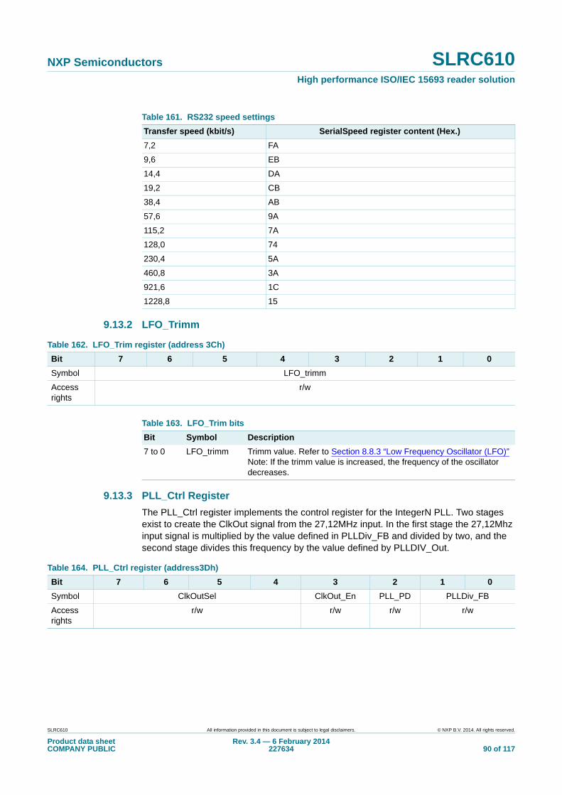
NXP Semiconductors SLRC610High performance ISO/IEC 15693 reader solution
9.13.2 LFO_Trimm
9.13.3 PLL_Ctrl Register
The PLL_Ctrl register implements the control register for the IntegerN PLL. Two stages exist to create the ClkOut signal from the 27,12MHz input. In the first stage the 27,12Mhz input signal is multiplied by the value defined in PLLDiv_FB and divided by two, and the second stage divides this frequency by the value defined by PLLDIV_Out.
Table 161. RS232 speed settings
Transfer speed (kbit/s) SerialSpeed register content (Hex.)
7,2 FA
9,6 EB
14,4 DA
19,2 CB
38,4 AB
57,6 9A
115,2 7A
128,0 74
230,4 5A
460,8 3A
921,6 1C
1228,8 15
Table 162. LFO_Trim register (address 3Ch)
Bit 7 6 5 4 3 2 1 0
Symbol LFO_trimm
Access rights
r/w
Table 163. LFO_Trim bits
Bit Symbol Description
7 to 0 LFO_trimm Trimm value. Refer to Section 8.8.3 “Low Frequency Oscillator (LFO)”Note: If the trimm value is increased, the frequency of the oscillator decreases.
Table 164. PLL_Ctrl register (address3Dh)
Bit 7 6 5 4 3 2 1 0
Symbol ClkOutSel ClkOut_En PLL_PD PLLDiv_FB
Access rights
r/w r/w r/w r/w
SLRC610 All information provided in this document is subject to legal disclaimers. © NXP B.V. 2014. All rights reserved.
Product data sheetCOMPANY PUBLIC
Rev. 3.4 — 6 February 2014227634 90 of 117

NXP Semiconductors SLRC610High performance ISO/IEC 15693 reader solution
9.13.4 PLLDiv_Out
Table 165. PLL_Ctrl register bits
Bit Symbol Description
7 to 4 CLkOutSel • 0h - pin CLKOUT is used as I/O
• 1h - pin CLKOUT shows the output of the analog PLL
• 2h - pin CLKOUT is hold on 0
• 3h - pin CLKOUT is hold on 1
• 4h - pin CLKOUT shows 27.12 MHz from the crystal
• 5h - pin CLKOUT shows 13.56 MHz derived from the crystal
• 6h - pin CLKOUT shows 6.78 MHz derived from the crystal
• 7h - pin CLKOUT shows 3.39 MHz derived from the crystal
• 8h - pin CLKOUT is toggled by the Timer0 overflow
• 9h - pin CLKOUT is toggled by the Timer1 overflow
• Ah - pin CLKOUT is toggled by the Timer2 overflow
• Bh - pin CLKOUT is toggled by the Timer3 overflow
• Ch...Fh - RFU
3 ClkOut_En Enables the clock at Pin CLKOUT
2 PLL_PD PLL power down
1-0 PLLDiv_FB PLL feedback divider (see table 174)
Table 166. Setting of feedback divider PLLDiv_FB [1:0]
Bit 1 Bit 0 Division
0 0 23 (VCO frequency 312Mhz)
0 1 27 (VCO frequency 366MHz)
1 0 28 (VCO frequency 380Mhz)
1 1 23 (VCO frequency 312Mhz)
Table 167. PLLDiv_Out register (address 3Eh)
Bit 7 6 5 4 3 2 1 0
Symbol PLLDiv_Out
Access rights
r/w
Table 168. PLLDiv_Out bits
Bit Symbol Description
7 to 0 PLLDiv_Out PLL output divider factor; Refer to Section 8.8.2
Table 169. Setting for the output divider ratio PLLDiv_Out [7:0]
Value Division
0 RFU
1 RFU
2 RFU
3 RFU
4 RFU
SLRC610 All information provided in this document is subject to legal disclaimers. © NXP B.V. 2014. All rights reserved.
Product data sheetCOMPANY PUBLIC
Rev. 3.4 — 6 February 2014227634 91 of 117

NXP Semiconductors SLRC610High performance ISO/IEC 15693 reader solution
9.14 Low-power card detection configuration registers
The LPCD registers contain the settings for the low-power card detection. The setting for LPCD_IMax (6 bits) is done by the two highest bits (bit 7, bit 6) of the registers LPCD_QMin, LPCD_QMax and LPCD_IMin each.
9.14.1 LPCD_QMin
9.14.2 LPCD_QMax
5 RFU
6 RFU
7 RFU
8 8
9 9
10 10
... ...
253 253
254 254
Table 169. Setting for the output divider ratio PLLDiv_Out [7:0]
Value Division
Table 170. LPCD_QMin register (address 3Fh)
Bit 7 6 5 4 3 2 1 0
Symbol LPCD_IMax.5 LPCD_IMax.4 LPCD_QMin
Access rights
r/w r/w r/w
Table 171. LPCD_QMin bits
Bit Symbol Description
7, 6 LPCD_IMax Defines the highest two bits of the higher border for the LPCD. If the measurement value of the I channel is higher than LPCD_IMax, a LPCD interrupt request is indicated by bit IRQ0.LPCDIrq.
5 to 0 LPCD_QMin Defines the lower border for the LPCD. If the measurement value of the Q channel is higher than LPCD_QMin, a LPCDinterrupt request is indicated by bit IRQ0.LPCDIrq.
Table 172. LPCD_QMax register (address 40h)
Bit 7 6 5 4 3 2 1 0
Symbol LPCD_IMax.3 LPCD_IMax.2 LPCD_QMax
Access rights
r/w r/w r/w
SLRC610 All information provided in this document is subject to legal disclaimers. © NXP B.V. 2014. All rights reserved.
Product data sheetCOMPANY PUBLIC
Rev. 3.4 — 6 February 2014227634 92 of 117
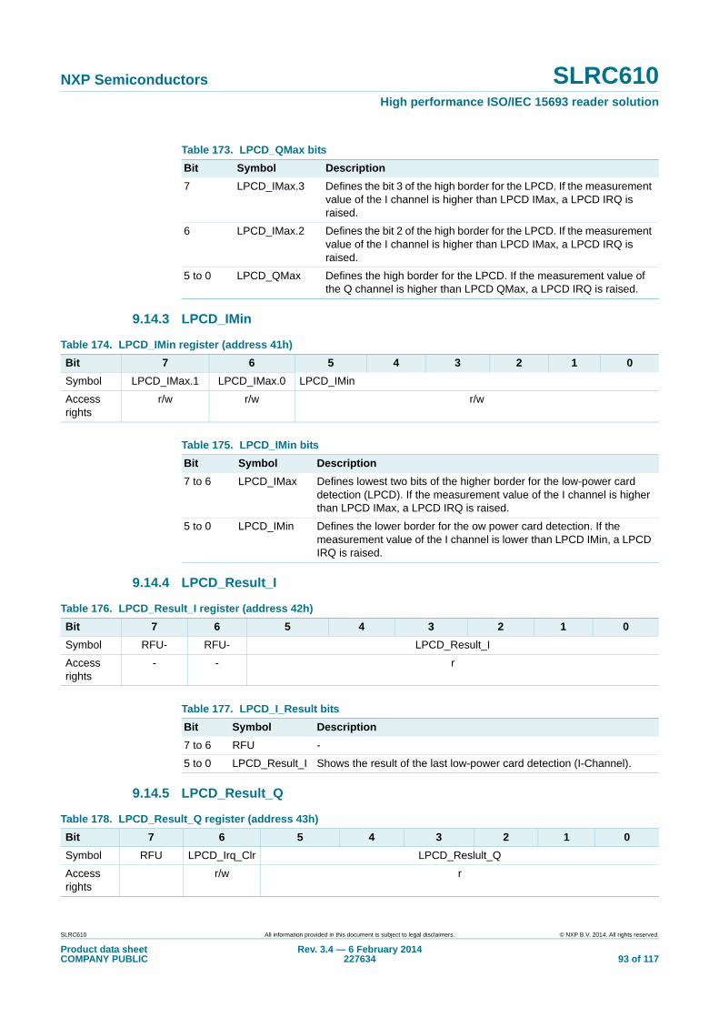
NXP Semiconductors SLRC610High performance ISO/IEC 15693 reader solution
9.14.3 LPCD_IMin
9.14.4 LPCD_Result_I
9.14.5 LPCD_Result_Q
Table 173. LPCD_QMax bits
Bit Symbol Description
7 LPCD_IMax.3 Defines the bit 3 of the high border for the LPCD. If the measurement value of the I channel is higher than LPCD IMax, a LPCD IRQ is raised.
6 LPCD_IMax.2 Defines the bit 2 of the high border for the LPCD. If the measurement value of the I channel is higher than LPCD IMax, a LPCD IRQ is raised.
5 to 0 LPCD_QMax Defines the high border for the LPCD. If the measurement value of the Q channel is higher than LPCD QMax, a LPCD IRQ is raised.
Table 174. LPCD_IMin register (address 41h)
Bit 7 6 5 4 3 2 1 0
Symbol LPCD_IMax.1 LPCD_IMax.0 LPCD_IMin
Access rights
r/w r/w r/w
Table 175. LPCD_IMin bits
Bit Symbol Description
7 to 6 LPCD_IMax Defines lowest two bits of the higher border for the low-power card detection (LPCD). If the measurement value of the I channel is higher than LPCD IMax, a LPCD IRQ is raised.
5 to 0 LPCD_IMin Defines the lower border for the ow power card detection. If the measurement value of the I channel is lower than LPCD IMin, a LPCD IRQ is raised.
Table 176. LPCD_Result_I register (address 42h)
Bit 7 6 5 4 3 2 1 0
Symbol RFU- RFU- LPCD_Result_I
Access rights
- - r
Table 177. LPCD_I_Result bits
Bit Symbol Description
7 to 6 RFU -
5 to 0 LPCD_Result_I Shows the result of the last low-power card detection (I-Channel).
Table 178. LPCD_Result_Q register (address 43h)
Bit 7 6 5 4 3 2 1 0
Symbol RFU LPCD_Irq_Clr LPCD_Reslult_Q
Access rights
r/w r
SLRC610 All information provided in this document is subject to legal disclaimers. © NXP B.V. 2014. All rights reserved.
Product data sheetCOMPANY PUBLIC
Rev. 3.4 — 6 February 2014227634 93 of 117

NXP Semiconductors SLRC610High performance ISO/IEC 15693 reader solution
9.15 Pin configuration
9.15.1 PinEn
9.15.2 PinOut
Table 179. LPCD_Q_Result bits
Bit Symbol Description
7 RFU -
6 LPCD_Irq_Clr If set no LPCD IRQ is raised any more until the next low-power card detection procedure. Can be used by software to clear the interrupt source.
5 to 0 LPCD_Result_Q Shows the result of the last ow power card detection (Q-Channel).
Table 180. PinEn register (address 44h)
Bit 7 6 5 4 3 2 1 0
Symbol SIGIN_EN CLKOUT_EN IFSEL1_EN IFSEL0_EN TCK_EN TMS_EN TDI_EN TMDO_EN
Access rights
r/w r/w r/w r/w r/w r/w r/w r/w
Table 181. PinEn bits
Bit Symbol Description
7 SIGIN_EN Enables the output functionality on SIGIN (pin 5). The pin is then used as I/O.
6 CLKOUT_EN Enables the output functionality of the CLKOUT (pin 22). The pin is then used as I/O. The CLKOUT function is switched off.
5 IFSEL1_EN Enables the output functionality of the IFSEL1 (pin 27). The pin is then used as I/O.
4 IFSEL0_EN Enables the output functionality of the IFSEL0 (pin 26). The pin is then used as I/O.
3 TCK_EN Enables the output functionality of the TCK (pin 4) of the boundary scan interface. The pin is then used as I/O. If the boundary scan is activated in EEPROM, this bit has no function.
2 TMS_EN Enables the output functionality of the TMS (pin 2) of the boundary scan interface. The pin is then used as I/O. If the boundary scan is activated in EEPROM, this bit has no function.
1 TDI_EN Enables the output functionality of the TDI (pin 1) of the boundary scan interface. The pin is then used as I/O. If the boundary scan is activated in EEPROM, this bit has no function.
0 TDO_EN Enables the output functionality of the TDO(pin 3) of the boundary scan interface. The pin is then used as I/O. If the boundary scan is activated in EEPROM, this bit has no function.
Table 182. PinOut register (address 45h)
Bit 7 6 5 4 3 2 1 0
Symbol SIGIN_OUT CLKOUT_OUT IFSEL1_OUT IFSEL0_OUT TCK_OUT
TMS_OUT
TDI_OUT TDO_OUT
Access rights
r/w r/w r/w r/w r/w r/w r/w r/w
SLRC610 All information provided in this document is subject to legal disclaimers. © NXP B.V. 2014. All rights reserved.
Product data sheetCOMPANY PUBLIC
Rev. 3.4 — 6 February 2014227634 94 of 117

NXP Semiconductors SLRC610High performance ISO/IEC 15693 reader solution
9.15.3 PinIn
9.15.4 SigOut
Table 183. PinOut bits
Bit Symbol Description
7 SIGIN_OUT Output buffer of the SIGIN pin
6 CLKOUT_OUT Output buffer of the CLKOUT pin
5 IFSEL1_OUT Output buffer of the IFSEL1 pin
4 IFSEL0_OUT Output buffer of the IFSEL0 pin
3 TCK_OUT Output buffer of the TCK pin
2 TMS_OUT Output buffer of the TMS pin
1 TDI_OUT Output buffer of the TDI pin
0 TDO_OUT Output buffer of the TDO pin
Table 184. PinIn register (address 46h)
Bit 7 6 5 4 3 2 1 0
Symbol SIGIN_IN CLKOUT_IN IFSEL1_IN IFSEL0_IN TCK_IN TMS_IN TDI_IN TDO_IN
Access rights
r r r r r r r r
Table 185. PinIn bits
Bit Symbol Description
7 SIGIN_IN Input buffer of the SIGIN pin
6 CLKOUT_IN Input buffer of the CLKOUT pin
5 IFSEL1_IN Input buffer of the IFSEL1 pin
4 IFSEL0_IN Input buffer of the IFSEL0 pin
3 TCK_IN Input buffer of the TCK pin
2 TMS_IN Input buffer of the TMS pin
1 TDI_IN Input buffer of the TDI pin
0 TDO_IN Input buffer of the TDO pin
Table 186. SigOut register (address 47h)
Bit 7 6 5 4 3 2 1 0
Symbol PadSpeed
RFU SigOutSel
Access rights
r/w - r/w
SLRC610 All information provided in this document is subject to legal disclaimers. © NXP B.V. 2014. All rights reserved.
Product data sheetCOMPANY PUBLIC
Rev. 3.4 — 6 February 2014227634 95 of 117

NXP Semiconductors SLRC610High performance ISO/IEC 15693 reader solution
9.16 Version register
9.16.1 Version
Table 187. SigOut bits
Bit Symbol Description
7 PadSpeed If set, the I/O pins are supporting a fast switching mode.The fast mode for the I/O’s will increase the peak current consumption of the device, especially if multiple I/Os are switching at the same time. The power supply needs to be designed to deliver this peak currents.
6 to 4 RFU -
3 to 0 SIGOutSel 0h, 1h - The pin SIGOUT is 3-state
2h - The pin SIGOUT is 0
3h - The pin SIGOUT is 1
4h - The pin SIGOUT shows the TX-envelope
5h - The pin SIGOUT shows the TX-active signal
6h - The pin SIGOUT shows the S3C (generic) signal
7h - The pin SIGOUT shows the RX-envelope (only valid for ISO/IEC 14443A, 106 kBd)8h - The pin SIGOUT shows the RX-active signal
9h - The pin SIGOUT shows the RX-bit signal
Table 188. Version register (address 7Fh)
Bit 7 6 5 4 3 2 1 0
Symbol Version SubVersion
Access rights
r r
Table 189. Version bits
Bit Symbol Description
7 to 4 Version Includes the version of the SLRC610 silicon.
3 to 0 SubVersion Includes the subversion of the SLRC610 silicon.
SLRC610 All information provided in this document is subject to legal disclaimers. © NXP B.V. 2014. All rights reserved.
Product data sheetCOMPANY PUBLIC
Rev. 3.4 — 6 February 2014227634 96 of 117

NXP Semiconductors SLRC610High performance ISO/IEC 15693 reader solution
10. Limiting values
11. Recommended operating conditions
[1] VDD(PVDD) must always be the same or lower than VDD.
12. Thermal characteristics
13. Characteristics
Table 190. Limiting valuesIn accordance with the Absolute Maximum Rating System (IEC 60134).
Symbol Parameter Conditions Min Max Unit
VDD supply voltage 0.5 +5.5 V
VDD(PVDD) PVDD supply voltage 0.5 +5.5 V
VDD(TVDD) TVDD supply voltage 0.5 +5.5 V
Vi(RXP) input voltage on pin RXP -0.5 +2.0 V
Vi(RXN) input voltage on pin RXN 0.5 +2.0 V
Ptot total power dissipation per package - 1125 mW
VESD(HBM) electrostatic discharge voltage Human Body Model (HBM); 1500 , 100 pF; JESD22-A114-B
- 2000 V
VESD(CDM) electrostatic discharge voltage Charge Device Model (CDM); - 500 V
Tj(max) maximum junction temperature
- 150 °C
Table 191. Operating conditions
Symbol Parameter Conditions Min Typ Max Unit
VDD supply voltage 3 5 5.5 V
VDD(TVDD) TVDD supply voltage [1] 3 5 5.5 V
VDD(PVDD) PVDD supply voltage 3 5 5.5 V
Tamb ambient temperature 25 - +85 C
Table 192. Thermal characteristics
Symbol Parameter Conditions Package Typ Unit
Rth(j-a) thermal resistance from junction to ambient
in still air with exposed pin soldered on a 4 layer JEDEC PCB
HVQFN32 40 K/W
Table 193. Characteristics
Symbol Parameter Conditions Min Typ Max Unit
Input characteristics I/O Pin Characteristics IF3-SDA in I2C configuration
ILI input leakage current output disabled - 2 100 nA
VIL LOW-level input voltage 0.5 - +0.3VDD(PVDD) V
VIH HIGH-level input voltage 0.7VDD(PVDD) - VDD(PVDD) + 0.5 V
VOL LOW-level output voltage IOL = 3 mA - - 0.3 V
SLRC610 All information provided in this document is subject to legal disclaimers. © NXP B.V. 2014. All rights reserved.
Product data sheetCOMPANY PUBLIC
Rev. 3.4 — 6 February 2014227634 97 of 117

NXP Semiconductors SLRC610High performance ISO/IEC 15693 reader solution
IOL LOW-level output current VOL = 0.4 V; Standard mode, Fast mode
4 - - mA
VOL = 0.6 V; Standard mode, Fast mode
6 - - mA
tf(o) output fall time Standard mode, Fast mode, CL < 400 pF
- - 250 ns
Fast mode +; CL < 550 pF - - 120 ns
tSP pulse width of spikes that must be suppressed by the input filter
0 - 50 ns
Ci input capacitance - 3.5 5 pF
CL load capacitance Standard mode - - 400 pF
Fast mode - - 550 pF
tEER EEPROM data retention
time
Tamb = +55 °C 10 - - year
NEEC EEPROM endurance
(number of programming
cycles)
under all operating
conditions
5 x 10⁵ - - cycle
Analog and digital supply AVDD,DVDD
VDDA analog supply voltage - 1.8 - V
VDDD digital supply voltage - 1.8 - V
CL load capacitance AVDD 220 470 - nF
CL load capacitance DVDD 220 470 - nF
Current consumption
Istb standby current Standby bit = 1 - 3 6 A
IDD supply current modem on - 17 20 mA
modem off - 0.45 0.5 mA
IDD(TVDD) TVDD supply current - 100 200 mA
I/O pin characteristics SIGIN, SIGOUT, CLKOUT, IFSEL0, IFSEL1, TCK, TMS, TDI, TDO, IRQ, IF0, IF1, IF2, SCL2, SDA2
ILI input leakage current output disabled - 50 500 nA
VIL LOW-level input voltage 0.5 - 0.3VDD(PVDD) V
VIH HIGH-level input voltage 0.7VDD(PVDD) - VDD(PVDD) + 0.5 V
VOL LOW-level output voltage IOL = 4 mA, VDD(PVDD) = 5.0 V
- - 0.4 V
IOL = 4 mA, VDD(PVDD) = 3.3 V
- - 0.4 V
VOH HIGH-level output voltage IOL = 4 mA, VDD(PVDD) = 5.0 V
4.6 - - V
IOL = 4 mA, VDD(PVDD) = 3.3 V
2.9 - - V
Ci input capacitance - 2.5 4.5 pF
Pull-up resistance for TCK, TMS, TDI, IF2
Rpu pull-up resistance 50 72 120 K
Table 193. Characteristics …continued
Symbol Parameter Conditions Min Typ Max Unit
SLRC610 All information provided in this document is subject to legal disclaimers. © NXP B.V. 2014. All rights reserved.
Product data sheetCOMPANY PUBLIC
Rev. 3.4 — 6 February 2014227634 98 of 117

NXP Semiconductors SLRC610High performance ISO/IEC 15693 reader solution
[1] Ipd is the total current for all supplies.
[2] IDD(PVDD) depends on the overall load at the digital pins.
[3] IDD(TVDD) depends on VDD(TVDD) and the external circuit connected to pins TX1 and TX2.
[4] During typical circuit operation, the overall current is below 100 mA.
[5] Typical value using a complementary driver configuration and an antenna matched to 40 between pins TX1 and TX2 at 13.56 MHz.
Pin characteristics AUX 1, AUX 2
Vo output voltage 0 - 1.8 V
CL load capacitance - - 400 pF
Pin characteristics RXP, RXN
Vi input voltage 0 - 1.8 V
Ci input capacitance 2 3.5 5 pF
Vmod(pp) modulation voltage Vmod(pp) = Vi(pp)(max) Vi(pp)
(min)
- 2.5 - mV
Vpp signal on RXP, RXN - - 1.65 V
Pins TX1 and TX2
Vo output voltage Vss(TVSS) - VDD(TVDD) V
Ro output resistance - 1.5 -
Current consumption
Ipd power-down current ambient temp = 25°C - 8 40 nA
ambient temp = 85°C - 200 400 nA
Istby standby current ambient temp = 25°C [1] - 3 6 A
ILPCD LPCD sleep current [1] - 3 6 A
IDD supply current - 17 20 mA
modem off; transceiver off - 0.45 0.5 mA
IDD(PVDD) PVDD supply current no load on digital pin [2] - - 10 A
IDD(TVDD) TVDD supply current [3][4][5] - 100 200 mA
Clock frequency Pin CLKOUT
fclk clock frequency configured to 27.12 MHz - 27.12 - MHz
clk clock duty cycle - 50 - %
Crystal oscillator
Vo(p-p) peak-to-peak output voltage
pin XTAL1 - 1 - V
Vi input voltage pin XTAL1 0 - 1.8 V
Ci input capacitance pin XTAL1 - 3 - pF
Typical input requirements
fxtal crystal frequency - 27.12 - MHz
ESR equivalent series resistance
- 50 100
CL load capacitance - 10 - pF
Pxtal crystal power dissipation - 50 100 W
Table 193. Characteristics …continued
Symbol Parameter Conditions Min Typ Max Unit
SLRC610 All information provided in this document is subject to legal disclaimers. © NXP B.V. 2014. All rights reserved.
Product data sheetCOMPANY PUBLIC
Rev. 3.4 — 6 February 2014227634 99 of 117

NXP Semiconductors SLRC610High performance ISO/IEC 15693 reader solution
13.1 Timing characteristics
Remark: To send more bytes in one data stream the NSS signal must be LOW during the send process. To send more than one data stream the NSS signal must be HIGH between each data stream.
Fig 28. Pin RX input voltage
001aak012
VMID
0 V
Vmod
Vi(p-p)(max) Vi(p-p)(min)
13.56 MHzcarrier
Table 194. SPI timing characteristics
Symbol Parameter Conditions Min Typ Max Unit
tSCKL SCK LOW time 50 - - ns
tSCKH SCK HIGH time 50 - - ns
th(SCKH-D) SCK HIGH to data input hold time
SCK to changing MOSI 25 - - ns
tsu(D-SCKH) data input to SCK HIGH set-up time
changing MOSI to SCK 25 - - ns
th(SCKL-Q) SCK LOW to data output hold time
SCK to changing MISO - - 25 ns
t(SCKL-NSSH) SCK LOW to NSS HIGH time
0 - - ns
tNSSH NSS HIGH time before communication 50 - - ns
Table 195. I2C-bus timing in fast mode and fast mode plus
Symbol Parameter Conditions Fast mode Fast mode Plus
Unit
Min Max Min Max
fSCL SCL clock frequency 0 400 0 1000 kHz
tHD;STA hold time (repeated) START condition
after this period, the first clock pulse is generated
600 - 260 - ns
tSU;STA set-up time for a repeated START condition
600 - 260 - ns
tSU;STO set-up time for STOP condition 600 - 260 - ns
tLOW LOW period of the SCL clock 1300 - 500 - ns
tHIGH HIGH period of the SCL clock 600 - 260 - ns
tHD;DAT data hold time 0 900 - 450 ns
SLRC610 All information provided in this document is subject to legal disclaimers. © NXP B.V. 2014. All rights reserved.
Product data sheetCOMPANY PUBLIC
Rev. 3.4 — 6 February 2014227634 100 of 117

NXP Semiconductors SLRC610High performance ISO/IEC 15693 reader solution
tSU;DAT data set-up time 100 - - - ns
tr rise time SCL signal 20 300 - 120 ns
tf fall time SCL signal 20 300 - 120 ns
tr rise time SDA and SCL signals
20 300 - 120 ns
tf fall time SDA and SCL signals
20 300 - 120 ns
tBUF bus free time between a STOP and START condition
1.3 - 0.5 - s
Fig 29. Timing for fast and standard mode devices on the I2C-bus
Table 195. I2C-bus timing in fast mode and fast mode plus …continued
Symbol Parameter Conditions Fast mode Fast mode Plus
Unit
Min Max Min Max
001aaj635
SDA
tf
SCL
tLOW tf
tSP tr
tHD;STAtHD;DAT
tHD;STA
tr tHIGH
tSU;DAT
S Sr P S
tSU;STA
tSU;STO
tBUF
SLRC610 All information provided in this document is subject to legal disclaimers. © NXP B.V. 2014. All rights reserved.
Product data sheetCOMPANY PUBLIC
Rev. 3.4 — 6 February 2014227634 101 of 117

NXP Semiconductors SLRC610High performance ISO/IEC 15693 reader solution
14. Application information
A typical application diagram using a complementary antenna connection to the SLRC610 is shown in Figure 30.
The antenna tuning and RF part matching is described in the application note Ref. 1 and Ref. 2.
14.1 Antenna design description
The matching circuit for the antenna consists of an EMC low pass filter (L0 and C0), a matching circuitry (C1 and C2), and a receiving circuits (R1 = R3, R2 = R4, C3 = C5 and C4 = C6;), and the antenna itself. The receiving circuit component values needs to be designed for operation with the SLRC610. A reuse of dedicated antenna designs done for other products without adaptation of component values will result in degraded performance.
For a more detailed information about designing and tuning the antenna, please refer to the relevant application notes:
• MICORE reader IC family; Directly Matched Antenna Design, Ref. 1 and
• MIFARE (14443A) 13.56 MHz RFID Proximity Antennas, Ref. 2.
14.1.1 EMC low pass filter
The MIFARE system operates at a frequency of 13.56 MHz. This frequency is derived from a quartz oscillator to clock the SLRC610 and is also the basis for driving the antenna with the 13.56 MHz energy carrier. This will not only cause emitted power at 13.56 MHz
Fig 30. Typical application antenna circuit diagram
001aam269
VDD PVDD
MICRO-PROCESSOR
hostinterface
TVDD
XTAL1 XTAL2
RXN
VMID
TX1
TVSS
TX2
9
8 25 18
19VSS
33 20
13
14
17
16
15
14
21
28-31
32
PDOWN
IRQ
7DVDD
AVDD
12RXP
READER IC
R1
L0 C1 Ra
RaC1L0
R2
R4
C0
C0
C2
C2
CRXN
CRXP
Cvmid
R3
27.12 MHz
antenna
Lant
SLRC610 All information provided in this document is subject to legal disclaimers. © NXP B.V. 2014. All rights reserved.
Product data sheetCOMPANY PUBLIC
Rev. 3.4 — 6 February 2014227634 102 of 117

NXP Semiconductors SLRC610High performance ISO/IEC 15693 reader solution
but will also emit power at higher harmonics. The international EMC regulations define the amplitude of the emitted power in a broad frequency range. Thus, an appropriate filtering of the output signal is necessary to fulfil these regulations.
Remark: The PCB layout has a major influence on the overall performance of the filter.
14.1.2 Antenna matching
Due to the impedance transformation of the given low pass filter, the antenna coil has to be matched to a certain impedance. The matching elements C1 and C2 can be estimated and have to be fine tuned depending on the design of the antenna coil.
The correct impedance matching is important to provide the optimum performance. The overall quality factor has to be considered to guarantee a proper ISO/IEC 14443 communication scheme. Environmental influences have to be considered as well as common EMC design rules.
For details refer to the NXP application notes.
14.1.3 Receiving circuit
The internal receiving concept of the SLRC610 makes use both side-bands of the sub-carrier load modulation of the card response via a differential receiving concept (RXP, RXN). No external filtering is required.
It is recommended to use the internally generated VMID potential as the input potential of pin RX. This DC voltage level of VMID has to be coupled to the Rx-pins via R2 and R4. To provide a stable DC reference voltage capacitances C4, C6 has to be connected between VMID and ground. Refer to Figure 30
Considering the (AC) voltage limits at the Rx-pins the AC voltage divider of R1 + C3 and R2 as well as R3 + C5 and R4 has to be designed. Depending on the antenna coil design and the impedance matching the voltage at the antenna coil varies from antenna design to antenna design. Therefore the recommended way to design the receiving circuit is to use the given values for R1(= R3), R2 (= R4), and C3 (= C5) from the above mentioned application note, and adjust the voltage at the RX-pins by varying R1(= R3) within the given limits.
Remark: R2 and R4 are AC-wise connected to ground (via C4 and C6).
SLRC610 All information provided in this document is subject to legal disclaimers. © NXP B.V. 2014. All rights reserved.
Product data sheetCOMPANY PUBLIC
Rev. 3.4 — 6 February 2014227634 103 of 117

NXP Semiconductors SLRC610High performance ISO/IEC 15693 reader solution
14.1.4 Antenna coil
The precise calculation of the antenna coils’ inductance is not practicable but the inductance can be estimated using the following formula. We recommend designing an antenna either with a circular or rectangular shape.
(4)
• I1 - Length in cm of one turn of the conductor loop
• D1 - Diameter of the wire or width of the PCB conductor respectively
• K - Antenna shape factor (K = 1,07 for circular antennas and K = 1,47 for square antennas)
• L1 - Inductance in nH
• N1 - Number of turns
• Ln: Natural logarithm function
The actual values of the antenna inductance, resistance, and capacitance at 13.56 MHz depend on various parameters such as:
• antenna construction (Type of PCB)
• thickness of conductor
• distance between the windings
• shielding layer
• metal or ferrite in the near environment
Therefore a measurement of those parameters under real life conditions, or at least a rough measurement and a tuning procedure is highly recommended to guarantee a reasonable performance. For details refer to the above mentioned application notes.
L1 2= I1
I1
D1------ ln K–
N11 8
SLRC610 All information provided in this document is subject to legal disclaimers. © NXP B.V. 2014. All rights reserved.
Product data sheetCOMPANY PUBLIC
Rev. 3.4 — 6 February 2014227634 104 of 117

NXP Semiconductors SLRC610High performance ISO/IEC 15693 reader solution
15. Package outline
Fig 31. Package outline SOT617-1 (HVQFN32)
0.51
A1 EhbUNIT ye
0.2
c
REFERENCESOUTLINEVERSION
EUROPEANPROJECTION ISSUE DATE
IEC JEDEC JEITA
mm 5.14.9
Dh
3.252.95
y1
5.14.9
3.252.95
e1
3.5
e2
3.50.300.18
0.050.00
0.05 0.1
DIMENSIONS (mm are the original dimensions)
SOT617-1 MO-220- - - - - -
0.50.3
L
0.1
v
0.05
w
0 2.5 5 mm
scale
SOT617-1HVQFN32: plastic thermal enhanced very thin quad flat package; no leads;32 terminals; body 5 x 5 x 0.85 mm
A(1)
max.
AA1
c
detail X
yy1 Ce
L
Eh
Dh
e
e1
b
9 16
32 25
24
178
1
X
D
E
C
B A
e2
terminal 1index area
terminal 1index area
01-08-0802-10-18
1/2 e
1/2 e ACC
Bv M
w M
E(1)
Note
1. Plastic or metal protrusions of 0.075 mm maximum per side are not included.
D(1)
SLRC610 All information provided in this document is subject to legal disclaimers. © NXP B.V. 2014. All rights reserved.
Product data sheetCOMPANY PUBLIC
Rev. 3.4 — 6 February 2014227634 105 of 117

NXP Semiconductors SLRC610High performance ISO/IEC 15693 reader solution
Detailed package information can be found at http://www.nxp.com/package/SOT617-1.html.
16. Handling information
Moisture Sensitivity Level (MSL) evaluation has been performed according to SNW-FQ-225B rev.04/07/07 (JEDEC J-STD-020C). MSL for this package is level 2 which means 260 C convection reflow temperature.
For MSL2:
• Dry pack is required.
• 1 year out-of-pack floor life at maximum ambient temperature 30 C/ 85 % RH.
For MSL1:
• No dry pack is required.
• No out-of-pack floor live spec. required.
17. Packing information
Fig 32. Packing information 1 tray
001aaj740
strap 46 mm from corner
tray
chamfer
PIN 1
chamfer
PIN 1
printed plano box
ESD warning preprinted
barcode label (permanent)
barcode label (peel-off)
QA seal
Hyatt patent preprinted
The straps around the package of stacked trays inside the plano-boxhave sufficient pre-tension to avoidloosening of the trays.
In the traystack (2 trays)only ONE tray type* allowed*one supplier and one revision number.
SLRC610 All information provided in this document is subject to legal disclaimers. © NXP B.V. 2014. All rights reserved.
Product data sheetCOMPANY PUBLIC
Rev. 3.4 — 6 February 2014227634 106 of 117

xxxxxxxxxxxxxxxxxxxxx xxxxxxxxxxxxxxxxxxxxxxxxxx xxxxxxx x x x xxxxxxxxxxxxxxxxxxxxxxxxxxxxxx xxxxxxxxxxxxxxxxxxx xx xx xxxxx xxxxxxxxxxxxxxxxxxxxxxxxxxx xxxxxxxxxxxxxxxxxxx xxxxxx xxxxxxxxxxxxxxxxxxxxxxxxxxxxxxxxxxx xxxxxxxxxxxx x x xxxxxxxxxxxxxxxxxxxxx xxxxxxxxxxxxxxxxxxxxxxxxxxxxxx xxxxx xxxxxxxxxxxxxxxxxxxxxxxxxxxxxxxxxxxxxxxxxxxxxxxxxx xxxxxxxx xxxxxxxxxxxxxxxxxxxxxxxxx xxxxxxxxxxxxxxxxxxxx xxx
SL
RC
610
Pro
du
ct data sh
CO
MP
AN
Y P
UB
L
NX
P S
emico
nd
ucto
rsS
LR
C610
Hig
h p
erform
an
ce
ISO
/IEC
15
693 rea
der s
olu
tion
aaa-004952
PQ-label (permanent) bag
strap 46 mm from the corner
dry-agent
ESD warning preprinted
PQ-label (permanent)
dry-pack ID preprinted
strap
QA seal
All inform
ation provided
in this docum
ent is subject to leg
al disclaim
ers.©
NX
P B
.V. 2014. A
ll rights reserved.
eetIC
Rev. 3.4 —
6 Feb
ruary 2014
227634 107 o
f 117
Fig 33. Packing information 5 tray
relative humidity indicator
traypreprinted:recycling symbolmoisture caution labelESD warning
manufacturer bag info
chamfer
chamfer
chamferprinted plano box
PIN 1
PIN 1
PIN 1
PLCC52

xxxxxxxxxxxxxxxxxxxxx xxxxxxxxxxxxxxxxxxxxxxxxxx xxxxxxx x x x xxxxxxxxxxxxxxxxxxxxxxxxxxxxxx xxxxxxxxxxxxxxxxxxx xx xx xxxxx xxxxxxxxxxxxxxxxxxxxxxxxxxx xxxxxxxxxxxxxxxxxxx xxxxxx xxxxxxxxxxxxxxxxxxxxxxxxxxxxxxxxxxx xxxxxxxxxxxx x x xxxxxxxxxxxxxxxxxxxxx xxxxxxxxxxxxxxxxxxxxxxxxxxxxxx xxxxx xxxxxxxxxxxxxxxxxxxxxxxxxxxxxxxxxxxxxxxxxxxxxxxxxx xxxxxxxx xxxxxxxxxxxxxxxxxxxxxxxxx xxxxxxxxxxxxxxxxxxxx xxx
SL
RC
610
Pro
du
ct data sh
CO
MP
AN
Y P
UB
L
NX
P S
emico
nd
ucto
rsS
LR
C610
Hig
h p
erform
an
ce
ISO
/IEC
15
693 rea
der s
olu
tion
BC
AN
AN
aaa-004949
BA
AM AM
BA
BB
K-AK:1
section AM-AMscale 4:1
section AN-ANscale 4:1
side lock
All inform
ation provided
in this docum
ent is subject to leg
al disclaim
ers.©
NX
P B
.V. 2014. A
ll rights reserved.
eetIC
Rev. 3.4 —
6 Feb
ruary 2014
227634 108 o
f 117
Fig 34. Tray details
BC
AK
AK
1.55
3.00
(0.3
0)
16.60±0.08+7°/S SQ.
1.20
0.56
3.32
(14.40+5°/S SQ.)
(1.4
5)
1.10
2.50
(0.6
4)
0.35
BB
BD BD
AJ
AR
AJ
AL ALAR
section BC-BCscale 4:1
vacuum cell
section BD-BDscale 4:1
section BA-BAscale 4:1
detail ACscale 20:1 section AJ-AJ
scale 2:1
section AR-ARscale 2:1
section AL-ALscale 5:1
section Ascale 5
end lock
12.80-5°/S SQ.
14.20±0.08+10°/S SQ.
13.85±0.08+12°/S SQ.
BA C0.50
BA C0.50

xxxxxxxxxxxxxxxxxxxxx xxxxxxxxxxxxxxxxxxxxxxxxxx xxxxxxx x x x xxxxxxxxxxxxxxxxxxxxxxxxxxxxxx xxxxxxxxxxxxxxxxxxx xx xx xxxxx xxxxxxxxxxxxxxxxxxxxxxxxxxx xxxxxxxxxxxxxxxxxxx xxxxxx xxxxxxxxxxxxxxxxxxxxxxxxxxxxxxxxxxx xxxxxxxxxxxx x x xxxxxxxxxxxxxxxxxxxxx xxxxxxxxxxxxxxxxxxxxxxxxxxxxxx xxxxx xxxxxxxxxxxxxxxxxxxxxxxxxxxxxxxxxxxxxxxxxxxxxxxxxx xxxxxxxx xxxxxxxxxxxxxxxxxxxxxxxxx xxxxxxxxxxxxxxxxxxxx xxx
SL
RC
610
Pro
du
ct data sh
CO
MP
AN
Y P
UB
L
NX
P S
emico
nd
ucto
rsS
LR
C610
Hig
h p
erform
an
ce
ISO
/IEC
15
693 rea
der s
olu
tion
aaa-004950
tape
guard band
END TO THE GUARD BAND, RE GUARD BAND
(see: HOW TO SECURE)see: ASSY REEL + LABELS
ASSY REEL + LABELS
Ø 330x12/16/24/32 (hub 7’’)
Ø 330x16/24/32/44 (hub 4’’)Ø 330x44 (hub 6’’)
Ø 180x12/16/24
r : lenght of trailer shall be 400 mm min. and covered with cover tape
circular sprocket hole side
guard band
: lenght of trailer shall be 160 mm min. and covered with cover tape
tapeth pull tabs on both ends)
guard band
lape double-backedonto itself on both ends
All inform
ation provided
in this docum
ent is subject to leg
al disclaim
ers.©
NX
P B
.V. 2014. A
ll rights reserved.
eetIC
Rev. 3.4 —
6 Feb
ruary 2014
227634 109 o
f 117
Fig 35. Packing information Reel
circular sprocket holesopposite the label side of reel
cover tape
carrier tape
enlongated
circular
enlongated
PIN1 has to bein quadrant 1
QA seal
preprinted ESD warning
PQ-label
dry-pack ID preprinted(permanent)
product orientationin carrier tape
product orientation ONLY for turnedproducts with 12nc ending 128
HOW TO SECURE LEADERHOW TO SECU
unreeling direction
(see: HOW TO SECURE)
PIN1
PIN1
PIN1 PIN1
BGAbare die
BGAbare die
for SOT505-2ending 125
for SOT765ending 125
PIN1 PIN1 PIN1
PIN1 PIN1QFPQFPPLCCSO SO
1 23 4
(HV)QFN(HV)SON(H)BCC
(HV)QFN(HV)SON(H)BCC
1 23 4
label side embossedESD logo
embossedESD logo
tape
printed plano-box
tapeslot
label side
trailer
leader
leade
trailer
(wi

NXP Semiconductors SLRC610High performance ISO/IEC 15693 reader solution
18. Abbreviations
Table 196. Abbreviations
Acronym Description
ADC Analog-to-Digital Converter
BPSK Binary Phase Shift Keying
CRC Cyclic Redundancy Check
CW Continuous Wave
EGT Extra Guard Time
EMC Electro Magnetic Compatibility
EMD Electro Magnetic Disturbance
EOF End Of Frame
EPC Electronic Product Code
ETU Elementary Time Unit
GPIO General Purpose Input/Output
HBM Human Body Model
I2C Inter-Integrated Circuit
LFO Low Frequency Oscillator
LPCD Low-Power Card Detection
LSB Least Significant Bit
MISO Master In Slave Out
MOSI Master Out Slave In
MSB Most Significant Bit
NRZ Not Return to Zero
NSS Not Slave Select
PCD Proximity Coupling Device
PLL Phase-Locked Loop
RZ Return To Zero
RX Receiver
SAM Secure Access Module
SOF Start Of Frame
SPI Serial Peripheral Interface
SW Software
TTimer Timing of the clk period
TX Transmitter
UART Universal Asynchronous Receiver Transmitter
UID Unique IDentification
VCO Voltage Controlled Oscillator
SLRC610 All information provided in this document is subject to legal disclaimers. © NXP B.V. 2014. All rights reserved.
Product data sheetCOMPANY PUBLIC
Rev. 3.4 — 6 February 2014227634 110 of 117

NXP Semiconductors SLRC610High performance ISO/IEC 15693 reader solution
19. References
[1] Application note — MFRC52x Reader IC Family Directly Matched Antenna Design
[2] Application note — MIFARE (ISO/IEC 14443 A) 13.56 MHz RFID Proximity Antennas
[3] BSDL File — Boundary scan description language file of the SLRC610
SLRC610 All information provided in this document is subject to legal disclaimers. © NXP B.V. 2014. All rights reserved.
Product data sheetCOMPANY PUBLIC
Rev. 3.4 — 6 February 2014227634 111 of 117

NXP Semiconductors SLRC610High performance ISO/IEC 15693 reader solution
20. Revision history
Table 197. Revision history
Document ID Release date Data sheet status Change notice Supersedes
SLRC610 v.3.4 20140206 Product data sheet - SLRC610 v.3.3
Modifications: • Typo corrected
SLRC610 v.3.3 20140204 Product data sheet - SLRC610 v.3.2
Modifications: • PVDD, TVDD data updated
• Information on FIFO size corrected
• Typing error corrected in description for LPCD
• WaterLevel and FIFOLength updated in register overview description
• WaterLevel and FIFOLength updated in register FIFOControl
• Waterlevel Register updated
• FIFOLength Register updated
• Section 9.15.2 “PinOut”: Pin Out register description corrected
SLRC610 v.3.2 20130910 Product data sheet - SLRC610 v.3.1
Modifications: • Update of EEPROM content
• Descriptive title changed
• Table 182 “PinOut register (address 45h)”: corrected
SLRC610 v.3.1 20120906 Product data sheet - -
SLRC610 All information provided in this document is subject to legal disclaimers. © NXP B.V. 2014. All rights reserved.
Product data sheetCOMPANY PUBLIC
Rev. 3.4 — 6 February 2014227634 112 of 117

NXP Semiconductors SLRC610High performance ISO/IEC 15693 reader solution
21. Legal information
21.1 Data sheet status
[1] Please consult the most recently issued document before initiating or completing a design.
[2] The term ‘short data sheet’ is explained in section “Definitions”.
[3] The product status of device(s) described in this document may have changed since this document was published and may differ in case of multiple devices. The latest product status information is available on the Internet at URL http://www.nxp.com.
21.2 Definitions
Draft — The document is a draft version only. The content is still under internal review and subject to formal approval, which may result in modifications or additions. NXP Semiconductors does not give any representations or warranties as to the accuracy or completeness of information included herein and shall have no liability for the consequences of use of such information.
Short data sheet — A short data sheet is an extract from a full data sheet with the same product type number(s) and title. A short data sheet is intended for quick reference only and should not be relied upon to contain detailed and full information. For detailed and full information see the relevant full data sheet, which is available on request via the local NXP Semiconductors sales office. In case of any inconsistency or conflict with the short data sheet, the full data sheet shall prevail.
Product specification — The information and data provided in a Product data sheet shall define the specification of the product as agreed between NXP Semiconductors and its customer, unless NXP Semiconductors and customer have explicitly agreed otherwise in writing. In no event however, shall an agreement be valid in which the NXP Semiconductors product is deemed to offer functions and qualities beyond those described in the Product data sheet.
21.3 Disclaimers
Limited warranty and liability — Information in this document is believed to be accurate and reliable. However, NXP Semiconductors does not give any representations or warranties, expressed or implied, as to the accuracy or completeness of such information and shall have no liability for the consequences of use of such information. NXP Semiconductors takes no responsibility for the content in this document if provided by an information source outside of NXP Semiconductors.
In no event shall NXP Semiconductors be liable for any indirect, incidental, punitive, special or consequential damages (including - without limitation - lost profits, lost savings, business interruption, costs related to the removal or replacement of any products or rework charges) whether or not such damages are based on tort (including negligence), warranty, breach of contract or any other legal theory.
Notwithstanding any damages that customer might incur for any reason whatsoever, NXP Semiconductors’ aggregate and cumulative liability towards customer for the products described herein shall be limited in accordance with the Terms and conditions of commercial sale of NXP Semiconductors.
Right to make changes — NXP Semiconductors reserves the right to make changes to information published in this document, including without limitation specifications and product descriptions, at any time and without notice. This document supersedes and replaces all information supplied prior to the publication hereof.
Suitability for use — NXP Semiconductors products are not designed, authorized or warranted to be suitable for use in life support, life-critical or safety-critical systems or equipment, nor in applications where failure or malfunction of an NXP Semiconductors product can reasonably be expected to result in personal injury, death or severe property or environmental damage. NXP Semiconductors and its suppliers accept no liability for inclusion and/or use of NXP Semiconductors products in such equipment or applications and therefore such inclusion and/or use is at the customer’s own risk.
Applications — Applications that are described herein for any of these products are for illustrative purposes only. NXP Semiconductors makes no representation or warranty that such applications will be suitable for the specified use without further testing or modification.
Customers are responsible for the design and operation of their applications and products using NXP Semiconductors products, and NXP Semiconductors accepts no liability for any assistance with applications or customer product design. It is customer’s sole responsibility to determine whether the NXP Semiconductors product is suitable and fit for the customer’s applications and products planned, as well as for the planned application and use of customer’s third party customer(s). Customers should provide appropriate design and operating safeguards to minimize the risks associated with their applications and products.
NXP Semiconductors does not accept any liability related to any default, damage, costs or problem which is based on any weakness or default in the customer’s applications or products, or the application or use by customer’s third party customer(s). Customer is responsible for doing all necessary testing for the customer’s applications and products using NXP Semiconductors products in order to avoid a default of the applications and the products or of the application or use by customer’s third party customer(s). NXP does not accept any liability in this respect.
Limiting values — Stress above one or more limiting values (as defined in the Absolute Maximum Ratings System of IEC 60134) will cause permanent damage to the device. Limiting values are stress ratings only and (proper) operation of the device at these or any other conditions above those given in the Recommended operating conditions section (if present) or the Characteristics sections of this document is not warranted. Constant or repeated exposure to limiting values will permanently and irreversibly affect the quality and reliability of the device.
Terms and conditions of commercial sale — NXP Semiconductors products are sold subject to the general terms and conditions of commercial sale, as published at http://www.nxp.com/profile/terms, unless otherwise agreed in a valid written individual agreement. In case an individual agreement is concluded only the terms and conditions of the respective agreement shall apply. NXP Semiconductors hereby expressly objects to applying the customer’s general terms and conditions with regard to the purchase of NXP Semiconductors products by customer.
No offer to sell or license — Nothing in this document may be interpreted or construed as an offer to sell products that is open for acceptance or the grant, conveyance or implication of any license under any copyrights, patents or other industrial or intellectual property rights.
Document status[1][2] Product status[3] Definition
Objective [short] data sheet Development This document contains data from the objective specification for product development.
Preliminary [short] data sheet Qualification This document contains data from the preliminary specification.
Product [short] data sheet Production This document contains the product specification.
SLRC610 All information provided in this document is subject to legal disclaimers. © NXP B.V. 2014. All rights reserved.
Product data sheetCOMPANY PUBLIC
Rev. 3.4 — 6 February 2014227634 113 of 117

NXP Semiconductors SLRC610High performance ISO/IEC 15693 reader solution
Quick reference data — The Quick reference data is an extract of the product data given in the Limiting values and Characteristics sections of this document, and as such is not complete, exhaustive or legally binding.
Export control — This document as well as the item(s) described herein may be subject to export control regulations. Export might require a prior authorization from competent authorities.
Non-automotive qualified products — Unless this data sheet expressly states that this specific NXP Semiconductors product is automotive qualified, the product is not suitable for automotive use. It is neither qualified nor tested in accordance with automotive testing or application requirements. NXP Semiconductors accepts no liability for inclusion and/or use of non-automotive qualified products in automotive equipment or applications.
In the event that customer uses the product for design-in and use in automotive applications to automotive specifications and standards, customer (a) shall use the product without NXP Semiconductors’ warranty of the product for such automotive applications, use and specifications, and (b) whenever customer uses the product for automotive applications beyond NXP Semiconductors’ specifications such use shall be solely at customer’s own risk, and (c) customer fully indemnifies NXP Semiconductors for any liability, damages or failed product claims resulting from customer design and use of the product for automotive applications beyond NXP Semiconductors’ standard warranty and NXP Semiconductors’ product specifications.
Translations — A non-English (translated) version of a document is for reference only. The English version shall prevail in case of any discrepancy between the translated and English versions.
21.4 Licenses
21.5 TrademarksNotice: All referenced brands, product names, service names and trademarks are the property of their respective owners.
I2C-bus — logo is a trademark of NXP B.V.
ICODE and I-CODE — are trademarks of NXP B.V.
22. Contact information
For more information, please visit: http://www.nxp.com
For sales office addresses, please send an email to: [email protected]
Purchase of NXP ICs with NFC technology
Purchase of an NXP Semiconductors IC that complies with one of the Near Field Communication (NFC) standards ISO/IEC 18092 and ISO/IEC 21481 does not convey an implied license under any patent right infringed by implementation of any of those standards.
SLRC610 All information provided in this document is subject to legal disclaimers. © NXP B.V. 2014. All rights reserved.
Product data sheetCOMPANY PUBLIC
Rev. 3.4 — 6 February 2014227634 114 of 117

NXP Semiconductors SLRC610High performance ISO/IEC 15693 reader solution
23. Contents
1 Introduction . . . . . . . . . . . . . . . . . . . . . . . . . . . . 1
2 General description . . . . . . . . . . . . . . . . . . . . . . 1
3 Features and benefits . . . . . . . . . . . . . . . . . . . . 1
4 Quick reference data . . . . . . . . . . . . . . . . . . . . . 2
5 Ordering information. . . . . . . . . . . . . . . . . . . . . 2
6 Block diagram . . . . . . . . . . . . . . . . . . . . . . . . . . 3
7 Pinning information. . . . . . . . . . . . . . . . . . . . . . 37.1 Pin description . . . . . . . . . . . . . . . . . . . . . . . . . 4
8 Functional description . . . . . . . . . . . . . . . . . . . 58.1 Interrupt controller . . . . . . . . . . . . . . . . . . . . . . 68.2 Timer module . . . . . . . . . . . . . . . . . . . . . . . . . . 88.2.1 Timer modes. . . . . . . . . . . . . . . . . . . . . . . . . . . 98.2.1.1 Time-Out- and Watch-Dog-Counter . . . . . . . . . 98.2.1.2 Wake-up timer . . . . . . . . . . . . . . . . . . . . . . . . . 98.2.1.3 Stop watch . . . . . . . . . . . . . . . . . . . . . . . . . . . . 98.2.1.4 Programmable one-shot timer . . . . . . . . . . . . . 98.2.1.5 Periodical trigger. . . . . . . . . . . . . . . . . . . . . . . . 98.3 Contactless interface unit . . . . . . . . . . . . . . . 108.3.1 ISO/IEC15693 functionality . . . . . . . . . . . . . . 108.3.2 EPC-UID/UID-OTP functionality . . . . . . . . . . . 128.3.3 ISO/IEC 18000-3 mode 3/ EPC Class-1 HF
functionality. . . . . . . . . . . . . . . . . . . . . . . . . . . 128.3.4 EPC Class-1 HF and ICODE . . . . . . . . . . . . . 128.3.4.1 Data encoding ICODE . . . . . . . . . . . . . . . . . . 128.4 Host interfaces . . . . . . . . . . . . . . . . . . . . . . . . 128.4.1 Host interface configuration . . . . . . . . . . . . . . 128.4.2 SPI interface . . . . . . . . . . . . . . . . . . . . . . . . . . 138.4.2.1 General . . . . . . . . . . . . . . . . . . . . . . . . . . . . . . 138.4.2.2 Read data . . . . . . . . . . . . . . . . . . . . . . . . . . . . 138.4.2.3 Write data . . . . . . . . . . . . . . . . . . . . . . . . . . . . 148.4.2.4 Address byte. . . . . . . . . . . . . . . . . . . . . . . . . . 148.4.2.5 Timing Specification SPI . . . . . . . . . . . . . . . . . 148.4.3 RS232 interface . . . . . . . . . . . . . . . . . . . . . . . 158.4.3.1 Selection of the transfer speeds . . . . . . . . . . . 158.4.3.2 Framing . . . . . . . . . . . . . . . . . . . . . . . . . . . . . 168.4.4 I2C-bus interface . . . . . . . . . . . . . . . . . . . . . . 188.4.4.1 General . . . . . . . . . . . . . . . . . . . . . . . . . . . . . . 188.4.4.2 I2C Data validity . . . . . . . . . . . . . . . . . . . . . . . 188.4.4.3 I2C START and STOP conditions . . . . . . . . . . 198.4.4.4 I2C byte format . . . . . . . . . . . . . . . . . . . . . . . . 198.4.4.5 I2C Acknowledge . . . . . . . . . . . . . . . . . . . . . . 208.4.4.6 I2C 7-bit addressing . . . . . . . . . . . . . . . . . . . . 208.4.4.7 I2C-register write access . . . . . . . . . . . . . . . . 218.4.4.8 I2C-register read access . . . . . . . . . . . . . . . . . 218.4.4.9 I2CL-bus interface. . . . . . . . . . . . . . . . . . . . . . 228.4.5 SAM interface I2C . . . . . . . . . . . . . . . . . . . . . . 238.4.5.1 SAM functionality . . . . . . . . . . . . . . . . . . . . . . 23
8.4.5.2 SAM connection. . . . . . . . . . . . . . . . . . . . . . . 248.4.6 Boundary scan interface . . . . . . . . . . . . . . . . 248.4.6.1 Interface signals. . . . . . . . . . . . . . . . . . . . . . . 258.4.6.2 Test Clock (TCK) . . . . . . . . . . . . . . . . . . . . . . 258.4.6.3 Test Mode Select (TMS) . . . . . . . . . . . . . . . . 258.4.6.4 Test Data Input (TDI) . . . . . . . . . . . . . . . . . . . 258.4.6.5 Test Data Output (TDO) . . . . . . . . . . . . . . . . . 258.4.6.6 Data register . . . . . . . . . . . . . . . . . . . . . . . . . 268.4.6.7 Boundary scan cell. . . . . . . . . . . . . . . . . . . . . 268.4.6.8 Boundary scan path . . . . . . . . . . . . . . . . . . . . 268.4.6.9 Boundary Scan Description Language (BSDL) 278.4.6.10 Non-IEEE1149.1 commands . . . . . . . . . . . . . 288.5 Buffer . . . . . . . . . . . . . . . . . . . . . . . . . . . . . . 298.5.1 Overview . . . . . . . . . . . . . . . . . . . . . . . . . . . . 298.5.2 Accessing the FIFO buffer . . . . . . . . . . . . . . . 298.5.3 Controlling the FIFO buffer . . . . . . . . . . . . . . 298.5.4 Status Information about the FIFO buffer. . . . 298.6 Analog interface and contactless UART . . . . 318.6.1 General . . . . . . . . . . . . . . . . . . . . . . . . . . . . . 318.6.2 TX transmitter . . . . . . . . . . . . . . . . . . . . . . . . 318.6.2.1 Overshoot protection . . . . . . . . . . . . . . . . . . . 338.6.2.2 Bit generator . . . . . . . . . . . . . . . . . . . . . . . . . 348.6.3 Receiver circuitry . . . . . . . . . . . . . . . . . . . . . . 348.6.3.1 General . . . . . . . . . . . . . . . . . . . . . . . . . . . . . 348.6.3.2 Block diagram . . . . . . . . . . . . . . . . . . . . . . . . 358.6.4 Active antenna concept . . . . . . . . . . . . . . . . . 368.6.5 Symbol generator. . . . . . . . . . . . . . . . . . . . . . 398.7 Memory . . . . . . . . . . . . . . . . . . . . . . . . . . . . . 398.7.1 Memory overview. . . . . . . . . . . . . . . . . . . . . . 398.7.2 EEPROM memory organization. . . . . . . . . . . 408.7.2.1 Product information and configuration -
Page 0 . . . . . . . . . . . . . . . . . . . . . . . . . . . . . . 418.7.3 EEPROM initialization content LoadProtocol . 438.8 Clock generation . . . . . . . . . . . . . . . . . . . . . . 458.8.1 Crystal oscillator. . . . . . . . . . . . . . . . . . . . . . . 458.8.2 IntegerN PLL clock line . . . . . . . . . . . . . . . . . 458.8.3 Low Frequency Oscillator (LFO) . . . . . . . . . . 468.9 Power management. . . . . . . . . . . . . . . . . . . . 478.9.1 Supply concept . . . . . . . . . . . . . . . . . . . . . . . 478.9.2 Power reduction mode . . . . . . . . . . . . . . . . . . 478.9.2.1 Power-down . . . . . . . . . . . . . . . . . . . . . . . . . . 478.9.2.2 Standby mode . . . . . . . . . . . . . . . . . . . . . . . . 478.9.2.3 Modem off mode . . . . . . . . . . . . . . . . . . . . . . 478.9.3 Low-Power Card Detection (LPCD) . . . . . . . . 488.9.4 Reset and start-up time . . . . . . . . . . . . . . . . . 488.10 Command set. . . . . . . . . . . . . . . . . . . . . . . . . 498.10.1 General . . . . . . . . . . . . . . . . . . . . . . . . . . . . . 498.10.2 Command set overview . . . . . . . . . . . . . . . . . 49
SLRC610 All information provided in this document is subject to legal disclaimers. © NXP B.V. 2014. All rights reserved.
Product data sheetCOMPANY PUBLIC
Rev. 3.4 — 6 February 2014227634 115 of 117
continued >>

NXP Semiconductors SLRC610High performance ISO/IEC 15693 reader solution
8.10.3 Command functionality . . . . . . . . . . . . . . . . . . 508.10.3.1 Idle command . . . . . . . . . . . . . . . . . . . . . . . . . 508.10.3.2 LPCD command . . . . . . . . . . . . . . . . . . . . . . . 508.10.3.3 AckReq command . . . . . . . . . . . . . . . . . . . . . 508.10.3.4 Receive command . . . . . . . . . . . . . . . . . . . . . 508.10.3.5 Transmit command . . . . . . . . . . . . . . . . . . . . . 508.10.3.6 Transceive command . . . . . . . . . . . . . . . . . . . 518.10.3.7 WriteE2 command . . . . . . . . . . . . . . . . . . . . . 518.10.3.8 WriteE2PAGE command . . . . . . . . . . . . . . . . 518.10.3.9 ReadE2 command . . . . . . . . . . . . . . . . . . . . . 518.10.3.10 LoadReg command . . . . . . . . . . . . . . . . . . . . 518.10.3.11 LoadProtocol command . . . . . . . . . . . . . . . . . 518.10.3.12 GetRNR command . . . . . . . . . . . . . . . . . . . . . 528.10.3.13 SoftReset command . . . . . . . . . . . . . . . . . . . . 52
9 SLRC610 registers. . . . . . . . . . . . . . . . . . . . . . 549.1 Register bit behavior. . . . . . . . . . . . . . . . . . . . 549.2 Command configuration . . . . . . . . . . . . . . . . . 579.2.1 Command . . . . . . . . . . . . . . . . . . . . . . . . . . . . 579.3 SAM configuration register . . . . . . . . . . . . . . . 579.3.1 HostCtrl. . . . . . . . . . . . . . . . . . . . . . . . . . . . . . 579.4 FIFO configuration register . . . . . . . . . . . . . . . 589.4.1 FIFOControl . . . . . . . . . . . . . . . . . . . . . . . . . . 589.4.2 WaterLevel . . . . . . . . . . . . . . . . . . . . . . . . . . . 589.4.3 FIFOLength . . . . . . . . . . . . . . . . . . . . . . . . . . 609.4.4 FIFOData . . . . . . . . . . . . . . . . . . . . . . . . . . . . 609.5 Interrupt configuration registers . . . . . . . . . . . 609.5.1 IRQ0 register . . . . . . . . . . . . . . . . . . . . . . . . . 619.5.2 IRQ1 register . . . . . . . . . . . . . . . . . . . . . . . . . 619.5.3 IRQ0En register . . . . . . . . . . . . . . . . . . . . . . . 629.5.4 IRQ1En . . . . . . . . . . . . . . . . . . . . . . . . . . . . . 629.6 Contactless interface configuration registers . 639.6.1 Error . . . . . . . . . . . . . . . . . . . . . . . . . . . . . . . . 639.6.2 Status . . . . . . . . . . . . . . . . . . . . . . . . . . . . . . . 649.6.3 RxBitCtrl . . . . . . . . . . . . . . . . . . . . . . . . . . . . 659.6.4 RxColl . . . . . . . . . . . . . . . . . . . . . . . . . . . . . . 679.7 Timer configuration registers . . . . . . . . . . . . . 689.7.1 TControl . . . . . . . . . . . . . . . . . . . . . . . . . . . . . 689.7.2 T0Control . . . . . . . . . . . . . . . . . . . . . . . . . . . . 689.7.2.1 T0ReloadHi. . . . . . . . . . . . . . . . . . . . . . . . . . . 699.7.2.2 T0ReloadLo . . . . . . . . . . . . . . . . . . . . . . . . . . 699.7.2.3 T0CounterValHi . . . . . . . . . . . . . . . . . . . . . . . 709.7.2.4 T0CounterValLo . . . . . . . . . . . . . . . . . . . . . . . 709.7.2.5 T1Control . . . . . . . . . . . . . . . . . . . . . . . . . . . . 709.7.2.6 T1ReloadHi. . . . . . . . . . . . . . . . . . . . . . . . . . . 719.7.2.7 T1ReloadLo . . . . . . . . . . . . . . . . . . . . . . . . . . 719.7.2.8 T1CounterValHi . . . . . . . . . . . . . . . . . . . . . . . 729.7.2.9 T1CounterValLo . . . . . . . . . . . . . . . . . . . . . . . 729.7.2.10 T2Control . . . . . . . . . . . . . . . . . . . . . . . . . . . . 729.7.2.11 T2ReloadHi. . . . . . . . . . . . . . . . . . . . . . . . . . . 739.7.2.12 T2ReloadLo . . . . . . . . . . . . . . . . . . . . . . . . . . 73
9.7.2.13 T2CounterValHi . . . . . . . . . . . . . . . . . . . . . . . 749.7.2.14 T2CounterValLoReg . . . . . . . . . . . . . . . . . . . 749.7.2.15 T3Control . . . . . . . . . . . . . . . . . . . . . . . . . . . . 749.7.2.16 T3ReloadHi . . . . . . . . . . . . . . . . . . . . . . . . . . 759.7.2.17 T3ReloadLo . . . . . . . . . . . . . . . . . . . . . . . . . . 759.7.2.18 T3CounterValHi . . . . . . . . . . . . . . . . . . . . . . . 769.7.2.19 T3CounterValLo . . . . . . . . . . . . . . . . . . . . . . . 769.7.2.20 T4Control . . . . . . . . . . . . . . . . . . . . . . . . . . . . 769.7.2.21 T4ReloadHi . . . . . . . . . . . . . . . . . . . . . . . . . . 779.7.2.22 T4ReloadLo . . . . . . . . . . . . . . . . . . . . . . . . . . 779.7.2.23 T4CounterValHi . . . . . . . . . . . . . . . . . . . . . . . 789.7.2.24 T4CounterValLo . . . . . . . . . . . . . . . . . . . . . . . 789.8 Transmitter configuration registers. . . . . . . . . 789.8.1 TxMode . . . . . . . . . . . . . . . . . . . . . . . . . . . . . 789.8.2 TxAmp . . . . . . . . . . . . . . . . . . . . . . . . . . . . . . 799.8.3 TxCon . . . . . . . . . . . . . . . . . . . . . . . . . . . . . . 799.8.4 Txl . . . . . . . . . . . . . . . . . . . . . . . . . . . . . . . . . 809.9 CRC configuration registers. . . . . . . . . . . . . . 809.9.1 TxCrcPreset . . . . . . . . . . . . . . . . . . . . . . . . . . 809.9.2 RxCrcCon . . . . . . . . . . . . . . . . . . . . . . . . . . . 819.10 Transmitter configuration registers. . . . . . . . . 829.10.1 TxDataNum . . . . . . . . . . . . . . . . . . . . . . . . . . 829.10.2 TxSym10BurstLen . . . . . . . . . . . . . . . . . . . . . 839.10.3 TxWaitCtrl . . . . . . . . . . . . . . . . . . . . . . . . . . . 839.10.4 TxWaitLo . . . . . . . . . . . . . . . . . . . . . . . . . . . . 859.11 FrameCon . . . . . . . . . . . . . . . . . . . . . . . . . . . 859.12 Receiver configuration registers . . . . . . . . . . 869.12.1 RxSofD. . . . . . . . . . . . . . . . . . . . . . . . . . . . . . 869.12.2 RxCtrl . . . . . . . . . . . . . . . . . . . . . . . . . . . . . . . 869.12.3 RxWait . . . . . . . . . . . . . . . . . . . . . . . . . . . . . . 879.12.4 RxThreshold. . . . . . . . . . . . . . . . . . . . . . . . . . 879.12.5 Rcv. . . . . . . . . . . . . . . . . . . . . . . . . . . . . . . . . 879.12.6 RxAna . . . . . . . . . . . . . . . . . . . . . . . . . . . . . . 889.13 Clock configuration . . . . . . . . . . . . . . . . . . . . 899.13.1 SerialSpeed . . . . . . . . . . . . . . . . . . . . . . . . . . 899.13.2 LFO_Trimm . . . . . . . . . . . . . . . . . . . . . . . . . . 909.13.3 PLL_Ctrl Register. . . . . . . . . . . . . . . . . . . . . . 909.13.4 PLLDiv_Out . . . . . . . . . . . . . . . . . . . . . . . . . . 919.14 Low-power card detection configuration
registers . . . . . . . . . . . . . . . . . . . . . . . . . . . . . 929.14.1 LPCD_QMin. . . . . . . . . . . . . . . . . . . . . . . . . . 929.14.2 LPCD_QMax . . . . . . . . . . . . . . . . . . . . . . . . . 929.14.3 LPCD_IMin. . . . . . . . . . . . . . . . . . . . . . . . . . . 939.14.4 LPCD_Result_I . . . . . . . . . . . . . . . . . . . . . . . 939.14.5 LPCD_Result_Q . . . . . . . . . . . . . . . . . . . . . . 939.15 Pin configuration . . . . . . . . . . . . . . . . . . . . . . 949.15.1 PinEn . . . . . . . . . . . . . . . . . . . . . . . . . . . . . . . 949.15.2 PinOut . . . . . . . . . . . . . . . . . . . . . . . . . . . . . . 949.15.3 PinIn. . . . . . . . . . . . . . . . . . . . . . . . . . . . . . . . 959.15.4 SigOut . . . . . . . . . . . . . . . . . . . . . . . . . . . . . . 959.16 Version register . . . . . . . . . . . . . . . . . . . . . . . 96
SLRC610 All information provided in this document is subject to legal disclaimers. © NXP B.V. 2014. All rights reserved.
Product data sheetCOMPANY PUBLIC
Rev. 3.4 — 6 February 2014227634 116 of 117
continued >>

NXP Semiconductors SLRC610High performance ISO/IEC 15693 reader solution
9.16.1 Version . . . . . . . . . . . . . . . . . . . . . . . . . . . . . . 96
10 Limiting values. . . . . . . . . . . . . . . . . . . . . . . . . 97
11 Recommended operating conditions. . . . . . . 97
12 Thermal characteristics . . . . . . . . . . . . . . . . . 97
13 Characteristics. . . . . . . . . . . . . . . . . . . . . . . . . 9713.1 Timing characteristics . . . . . . . . . . . . . . . . . . 100
14 Application information. . . . . . . . . . . . . . . . . 10214.1 Antenna design description . . . . . . . . . . . . . 10214.1.1 EMC low pass filter . . . . . . . . . . . . . . . . . . . . 10214.1.2 Antenna matching. . . . . . . . . . . . . . . . . . . . . 10314.1.3 Receiving circuit . . . . . . . . . . . . . . . . . . . . . . 10314.1.4 Antenna coil . . . . . . . . . . . . . . . . . . . . . . . . . 104
15 Package outline . . . . . . . . . . . . . . . . . . . . . . . 105
16 Handling information. . . . . . . . . . . . . . . . . . . 106
17 Packing information . . . . . . . . . . . . . . . . . . . 106
18 Abbreviations. . . . . . . . . . . . . . . . . . . . . . . . . 110
19 References . . . . . . . . . . . . . . . . . . . . . . . . . . . 111
20 Revision history. . . . . . . . . . . . . . . . . . . . . . . 112
21 Legal information. . . . . . . . . . . . . . . . . . . . . . 11321.1 Data sheet status . . . . . . . . . . . . . . . . . . . . . 11321.2 Definitions. . . . . . . . . . . . . . . . . . . . . . . . . . . 11321.3 Disclaimers . . . . . . . . . . . . . . . . . . . . . . . . . . 11321.4 Licenses . . . . . . . . . . . . . . . . . . . . . . . . . . . . 11421.5 Trademarks. . . . . . . . . . . . . . . . . . . . . . . . . . 114
22 Contact information. . . . . . . . . . . . . . . . . . . . 114
23 Contents . . . . . . . . . . . . . . . . . . . . . . . . . . . . . 115
© NXP B.V. 2014. All rights reserved.
For more information, please visit: http://www.nxp.comFor sales office addresses, please send an email to: [email protected]
Date of release: 6 February 2014227634
Please be aware that important notices concerning this document and the product(s)described herein, have been included in section ‘Legal information’.