Embed Size (px)
Citation preview
IN
STAT1 CE
OUT
Li-Ion or Li-Pol
Battery Pack
+
Pack-
Pack+
STAT2
Vss ISET
PG
RED
GREEN
RSET
TMR
RTMR
1
2
3
4
5 6
7
8
9
10
BAT
Charge Enable
and Power Good
Input Power
R2
1.5 kW
R1
1.5 kW
bq24085
1 FmC2
49.9 kW
1.13 kW
C3
4.7 Fm
Product
Folder
Sample &Buy
Technical
Documents
Tools &
Software
Support &Community
bq24085, bq24086, bq24087, bq24088SLUS784E –DECEMBER 2007–REVISED DECEMBER 2015
bq2408x 750-mA Single-Chip Li-Ion and Li-Pol Charge Management ICWith Thermal Regulation
1 Features 3 DescriptionThe bq2408x series are highly integrated Li-Ion and
1• Ideal for Low-Dropout Designs for Single-Cell Li-Li-Pol linear chargers, targeted at space-limitedIon or Li-Pol Packs in Space Limited Applicationsportable applications. The bq2408x series offers a
• Integrated Power FET and Current Sensor for up variety of protection features and functional options,to 750-mA Charge Applications while still implementing a complete charging system
in a small package. The battery is charged in three• Reverse Leakage Protection Prevents Batteryphases: conditioning, constant or thermally regulatedDrainagecurrent, and constant voltage. Charge is terminated• ±0.5% Voltage Regulation Accuracy based on minimum current. An internal
• Thermal Regulation Maximizes Charge Rate programmable charge timer provides a backup• Charge Termination by Minimum Current and protection feature for charge termination and is
dynamically adjusted during the thermal regulationTimephase. The bq2408x automatically restarts the charge• Precharge Conditioning With Safety Timerif the battery voltage falls below an internal threshold;
• Status Outputs for LED or System Interface sleep mode is set when the external input supply isIndicate Charge, Fault, and Power Good Outputs removed. Multiple versions of this device family
enable easy design of the bq2408x in cradle chargers• Short-Circuit and Thermal Protectionor in the end equipment, while using low cost or high-• Automatic Sleep Mode for Low Powerend AC adapters.Consumption
• Small 3×3 mm MLP Package Device Information(1)
• Selectable Battery Insertion and Battery Absent PART NUMBER PACKAGE BODY SIZE (NOM)Detection bq2408x VSON (10) 3.00 mm × 3.00 mm
• Input Overvoltage Protection (1) For all available packages, see the orderable addendum atthe end of the data sheet.– 6.5 V and 10.5 V Options
2 Applications• PDA, MP3 Players, Digital Cameras• Internet Appliances and Handheld Devices
Typical Application Circuit
1
An IMPORTANT NOTICE at the end of this data sheet addresses availability, warranty, changes, use in safety-critical applications,intellectual property matters and other important disclaimers. PRODUCTION DATA.

bq24085, bq24086, bq24087, bq24088SLUS784E –DECEMBER 2007–REVISED DECEMBER 2015 www.ti.com
Table of Contents8.3 Feature Description................................................. 141 Features .................................................................. 18.4 Device Functional Modes........................................ 222 Applications ........................................................... 1
9 Application and Implementation ........................ 253 Description ............................................................. 19.1 Application Information............................................ 254 Revision History..................................................... 29.2 Typical Applications ................................................ 255 Device Options....................................................... 3
10 Power Supply Recommendations ..................... 296 Pin Configuration and Functions ......................... 411 Layout................................................................... 297 Specifications......................................................... 5
11.1 Layout Guidelines ................................................. 297.1 Absolute Maximum Ratings ...................................... 511.2 Layout Example .................................................... 297.2 ESD Ratings.............................................................. 511.3 Thermal Considerations ........................................ 307.3 Recommended Operating Conditions....................... 5
12 Device and Documentation Support ................. 317.4 Thermal Information .................................................. 512.1 Documentation Support ....................................... 317.5 Electrical Characteristics........................................... 612.2 Related Links ........................................................ 317.6 Timing Requirements ................................................ 812.3 Community Resources.......................................... 317.7 Dissipation Ratings ................................................... 812.4 Trademarks ........................................................... 317.8 Typical Characteristics .............................................. 912.5 Electrostatic Discharge Caution............................ 318 Detailed Description ............................................ 1112.6 Glossary ................................................................ 318.1 Overview ................................................................. 11
13 Mechanical, Packaging, and Orderable8.2 Functional Block Diagram ....................................... 13Information ........................................................... 31
4 Revision HistoryNOTE: Page numbers for previous revisions may differ from page numbers in the current version.
Changes from Revision D (August 2009) to Revision E Page
• Added ESD Ratings table, Feature Description section, Device Functional Modes, Application and Implementationsection, Power Supply Recommendations section, Layout section, Device and Documentation Support section, andMechanical, Packaging, and Orderable Information section .................................................................................................. 1
2 Submit Documentation Feedback Copyright © 2007–2015, Texas Instruments Incorporated
Product Folder Links: bq24085 bq24086 bq24087 bq24088

bq24085, bq24086, bq24087, bq24088www.ti.com SLUS784E –DECEMBER 2007–REVISED DECEMBER 2015
5 Device Options
PACKSAFETY POWERCHARGE INPUT TERMINATION IC PACK VOLTAGETIMER GOOD DEVICES (1) (2)VOLTAGE OVERVOLTAGE ENABLE ENABLE TEMP DETECTIONENABLE STATUS (ABSENT)
bq24086DRCRWith timer4.2 V 6.5 V TMR pin TMR pin PG pin No TS pin enabled bq24086DRCTbq24085DRCRWith timer4.2 V 6.5 V TMR pin TMR pin PG pin CE pin No enabled bq24085DRCT
With bq24087DRCR4.2 V 6.5 V TE pin TMR pin No CE pin No termination
bq24087DRCTenabledbq24088DRCRWith timer4.2 V 10.5 V TMR pin TMR pin PG pin No TS pin enabled bq24088DRCT
(1) The bq24085/6/7/8 are only available taped and reeled. Add suffix R to the part number for quantities of 3,000 devices per reel (forexample, bq24085DRCR). Add suffix T to the part number for quantities of 250 devices per reel (for example, bq24085/6/7DRCT).
(2) This product is RoHS compatible, including a lead concentration that does not exceed 0.1% of total product weight, and is suitable foruse in specified lead-free soldering processes. In addition, this product uses package materials that do not contain halogens, includingbromine (Br) or antimony (Sb) above 0.1% of total product weight.
Copyright © 2007–2015, Texas Instruments Incorporated Submit Documentation Feedback 3
Product Folder Links: bq24085 bq24086 bq24087 bq24088

1 IN
2 TMR
3 STAT 1
4 STAT 2
5 VSS
10
9
8
7
6
OUT
BAT
TE
CE
ISET
1 IN
2 TMR
3 STAT 1
4 STAT 2
5 VSS
10
9
8
7
6
OUT
BAT
CE
PG
ISET
1 IN
2 TMR
3 STAT 1
4 STAT 2
5 VSS
10
9
8
7
6
OUT
BAT
TS
PG
ISET
bq24085, bq24086, bq24087, bq24088SLUS784E –DECEMBER 2007–REVISED DECEMBER 2015 www.ti.com
6 Pin Configuration and Functions
bq24086 and bq24088 DRC Packagebq24085 DRC Package10-Pin VSON
10-Pin VSONTop ViewTop View
bq24087 DRC Package10-Pin VSON
Top View
Pin FunctionsPIN
I/O DESCRIPTIONNAME bq24086/8 bq24085 bq24087
Battery voltage sense input. Connect to the battery positive terminal. ConnectBAT 9 9 9 I a 390-Ω resistor from BAT to OUT for I(OUT) < 200 mA.CE – 8 7 I Charge enable input. CE = LO enables charger. CE = HI disables charger.
Charge input voltage and internal supply. Connect a 1-μF (minimum)IN 1 1 1 I capacitor from IN to VSS. CIN ≥ COUT
Charge current set point, resistor connected from ISET to VSS sets chargeISET 6 6 6 O current value. Connect a 0.1-μF capacitor from BAT to ISET for I(OUT) < 200
mA.Charge current output. Connect to the battery positive terminal. Connect a 1-OUT 10 10 10 O μF (minimum) capacitor from OUT to VSS.
PG 7 7 O Power good status output (open-collector), active low.STAT1 3 3 3 O Charge status output 1 (open-collector, see Table 3).STAT2 4 4 4 O Charge status output 2 (open-collector, see Table 3).
Termination enable input. TE = LO enables termination detection and batteryTE – – 8 I absent detection. TE = HI disables termination detection and battery absent
detection.Safety timer program input, timer disabled if floating. Connect a resistor toTMR 2 2 2 I VSS pin to program safety timer timeout value.Temperature sense input, connect to battery pack thermistor. Connect anTS 8 – – I external resistive divider to program temperature thresholds.
VSS 5 5 5 I GroundThere is an internal electrical connection between the exposed thermal pad
Exposed and Vss pin of the IC. The exposed thermal pad must be connected to theThermal Pad Pad Pad – same potential as the VSS pin on the printed circuit board. Do not use thePad thermal pad as the primary ground input for the IC. VSS pin must be
connected to ground at all times.
4 Submit Documentation Feedback Copyright © 2007–2015, Texas Instruments Incorporated
Product Folder Links: bq24085 bq24086 bq24087 bq24088

bq24085, bq24086, bq24087, bq24088www.ti.com SLUS784E –DECEMBER 2007–REVISED DECEMBER 2015
7 Specifications
7.1 Absolute Maximum Ratings (1)
MIN MAX UNITSupply voltage (IN with respect to Vss) –0.3 20 V (2)
Input voltage on IN, STATx, PG, TS, CE, TMR (all with respect to Vss) –0.3 V(IN) VInput voltage on OUT, BAT, ISET (all with respect to Vss) –0.3 7 VOutput sink current (STATx) + PG 15 mAOutput current (OUT pin) 2 A
TA Operating free-air temperature –40 155 °CTJ Junction temperature –40 150 °CTstg Storage temperature –65 150 °C
(1) Stresses beyond those listed under Absolute Maximum Ratings may cause permanent damage to the device. These are stress ratingsonly, and functional operation of the device at these or any other conditions beyond those indicated under Recommended OperatingConditions is not implied. Exposure to absolute–maximum–rated conditions for extended periods may affect device reliability.
(2) The bq24085/6/7/8 family can withstand up to 18 V maximum continuously, 20 V for maximum of 2000 hours and 26 V for a maximumfor 87 hours.
7.2 ESD RatingsVALUE UNIT
Human-body model (HBM), per ANSI/ESDA/JEDEC JS-001 (1) ±3000V(ESD) Electrostatic discharge V
Charged-device model (CDM), per JEDEC specification JESD22-C101 (2) ±1500
(1) JEDEC document JEP155 states that 500-V HBM allows safe manufacturing with a standard ESD control process.(2) JEDEC document JEP157 states that 250-V CDM allows safe manufacturing with a standard ESD control process.
7.3 Recommended Operating ConditionsMIN MAX UNIT
V(IN) Supply voltage Battery absent detection not functional 3.5 4.35 VV(IN) Supply voltage Battery absent detection functional 4.35 6.5 VR(TMR) Safety timer program resistor 33 100 KΩTJ Junction temperature 0 125 °C
7.4 Thermal Informationbq2408x
THERMAL METRIC (1) DRC (VSON) UNIT10 PINS
RθJA Junction-to-ambient thermal resistance 46.7 °C/WRθJC(top) Junction-to-case (top) thermal resistance 65.9 °C/WRθJB Junction-to-board thermal resistance 21.3 °C/WψJT Junction-to-top characterization parameter 1.6 °C/WψJB Junction-to-board characterization parameter 21.4 °C/WRθJC(bot) Junction-to-case (bottom) thermal resistance 3.6 °C/W
(1) For more information about traditional and new thermal metrics, see the Semiconductor and IC Package Thermal Metrics applicationreport, SPRA953.
Copyright © 2007–2015, Texas Instruments Incorporated Submit Documentation Feedback 5
Product Folder Links: bq24085 bq24086 bq24087 bq24088

bq24085, bq24086, bq24087, bq24088SLUS784E –DECEMBER 2007–REVISED DECEMBER 2015 www.ti.com
7.5 Electrical Characteristicsover recommended operating range, TJ = 0 –125°C range, See the Application and Implementation section, typical values atTJ = 25°C (unless otherwise noted), RTMR = 49.9 KΩ
PARAMETER TEST CONDITIONS MIN TYP MAX UNITPOWER DOWN THRESHOLD – UNDERVOLTAGE LOCKOUT
V(IN) = 0 V, increase V(OUT): 0 → 3 V ORVUVLO Power down threshold V(OUT) = 0 V, increase V(IN): 0 → 3 V, 1.5 3 V
CE = LO (1)
INPUT POWER DETECTION (2)
VIN(DT) Input power detection threshold V(IN) detected at [V(IN) – V(OUT)] > VIN(DT) 130 mVInput power not detected atVHYS(INDT) Input power detection hysteresis 30 mV[V(IN) – V(OUT)] < [VIN(DT) – VHYS(INDT)]
INPUT OVERVOLTAGE PROTECTIONbq24088 10.2 10.5 11.7
V(OVP) Input overvoltage detection threshold V(IN) increasing Vbq24085/6/7 6.2 6.5 7bq24088 0.5
VHYS(OVP) Input overvoltage hysteresis V(IN) decreasing Vbq24085/6/7 0.2
QUIESCENT CURRENTV(IN) = 6 V 100 200Input power detected,ICC(CHGOFF) IN pin quiescent current, charger off μACE = HI V(IN) = 16.5 V 350
ICC(CHGON) IN pin quiescent current, charger on Input power detected, CE = LO, VBAT = 4.5 V 4 6 mABattery leakage current after Input power detected, charge terminated,IBAT(DONE) 1 5 μAtermination into IC CE = LOBattery leakage current into IC, charger Input power detected, CE = HI ORIBAT(CHGOFF) 1 5 μAoff input power not detected, CE = LO
TS PIN COMPARATORV(TS1) Lower voltage temperature threshold Hot detected at V(TS) < V(TS1); NTC thermistor 29 30 31 %V(IN)V(TS2) Upper voltage temperature threshold Cold detected at V(TS) > V(TS2); NTC thermistor 60 61 62 %V(IN)
Temp OK at V(TS) > [ V(TS1) + VHYS(TS) ] ORVHYS(TS) Hysteresis 2 %V(IN)V(TS) < [ V(TS2) – VHYS(TS) ]CE INPUTVIL Input (low) voltage V(/CE) 0 1 VVIH Input (high) voltage V(/CE) 2 VSTAT1, STAT2 AND PG OUTPUTS (3)
VOL Output (low) saturation voltage Iout = 1 mA (sink) 200 mVTHERMAL SHUTDOWNT(SHUT) Temperature trip Junction temperature, temp rising 155 °CT(SHUTHYS) Thermal hysteresis Junction temperature 20 °CVOLTAGE REGULATION (4)
VO(REG) Output voltage 4.20 VTA = 25°C –0.5% 0.5%
VO(TOL) Voltage regulation accuracy–1% 1%
V(DO) Dropout voltage, V(IN) – V(OUT) I(OUT) = 750 mA 600 mVCURRENT REGULATION (5)
V(BAT) > V(LOWV), IO(OUT) = I(OUT) = K(SET) ×IO(OUT) Output current range 50 750 mAV(SET)/R(SET)
V(SET) Output current set voltage V(ISET) = V(SET), V(LOWV) < V(BAT) ≤ VO(REG) 2.45 2.5 2.55 V
(1) Specified by design, not production tested.(2) CE = HI or LOW, V(IN) > 3.5 V(3) V(IN) ≥ VO(REG) + V(DO-MAX)(4) V(IN) ≥ VO(REG) + V(DO-MAX), I(TERM) < I(OUT) < IO(OUT), charger enabled, no fault conditions detected.(5) V(IN) > V(OUT) > V(DO-MAX), charger enabled, no fault conditions detected.
6 Submit Documentation Feedback Copyright © 2007–2015, Texas Instruments Incorporated
Product Folder Links: bq24085 bq24086 bq24087 bq24088

bq24085, bq24086, bq24087, bq24088www.ti.com SLUS784E –DECEMBER 2007–REVISED DECEMBER 2015
Electrical Characteristics (continued)over recommended operating range, TJ = 0 –125°C range, See the Application and Implementation section, typical values atTJ = 25°C (unless otherwise noted), RTMR = 49.9 KΩ
PARAMETER TEST CONDITIONS MIN TYP MAX UNIT100 mA ≤ IO(OUT) ≤ 750 mA 175 182 190
K(SET) Output current set factor10 mA ≤ IO(OUT) < 100 mA 180 215 250
RISET External resistor range Resistor connected to ISET pin 0.6 10 kΩPRECHARGE AND OUTPUT SHORT-CIRCUIT CURRENT REGULATION (6)
Precharge to fast-charge transitionV(LOWV) V(BAT) increasing 2.8 2.95 3.15 VthresholdPrecharge to short-circuit transitionV(SC) V(BAT) decreasing 1.2 1.4 1.6threshold V
V(SCIND) Short-circuit indication V(BAT) decreasing 1.6 1.8 2V(SC) < VI(BAT) < V(LOWV), t < t(PRECHG)IO(PRECHG) Precharge current range 5 75 mAIO(PRECHG) = K(SET) × V(PRECHG)/R(ISET)
V(ISET) = V(PRECHG), V(SC) < VI(BAT) < V(LOWV),V(PRECHG) Precharge set voltage 225 250 280 mVt < t(PRECHG)
VPOR < VIN <VSS ≤ V(BAT) ≤ V(SCI), 7 15 246.0 VIO(SHORT) = I(OUT), V(BAT)= VSS,IO(SHORT) Output shorted regulation current mAInternal pullup resistor, 6.0 V < VIN < 15TJ = 25°C VOVP
TEMPERATURE REGULATION (Thermal regulation™) (7)
V(IN) = 5.5 V, V(BAT) = 3.2 V, Fast charge currentTJ(REG) Temperature regulation limit 101 112 125 °Cset to 1 AV(LOWV) < V(BAT) < VO(REG),I(MIN_TJ(REG)) Minimum current in thermal regulation 105 125 mA0.7 kΩ < R(ISET) < 1.18 kΩ
CHARGE TERMINATION DETECTION (8)
I(TERM) Termination detection current range V(BAT) > V(RCH), I(TERM) = K(SET) × V(TERM)/R(ISET) 5 75 mACharge termination detection setV(TERM) V(BAT) > V(RCH) 225 250 275 mVvoltage (9)
BATTERY RECHARGE THRESHOLDV(RCH) Recharge threshold detection [VO(REG)–V(BAT) ] > V(RCH) 75 100 135 mVTIMERS (10)
Charge timer and termination enable Charge timer AND termination bq24085/86/88threshold disabled at: V(TMR) > VTMR(OFF)VTMR(OFF) 2.5 3 3.5 VCharge timer disabled at:Charge timer enable threshold bq24087V(TMR) > VTMR(OFF)
BATTERY DETECTION THRESHOLDSIDET(DOWN) Battery detection current (sink) 2 V < V(BAT) < VO(REG) 1 2 3.2 mA
IO(PRIDET(UP) Battery detection current (source) 2 V < V(BAT) < VO(REG) mAECHG)
TIMER FAULT RECOVERYI(FAULT) Fault Current (source) V(OUT) < V(RCH) 0.8 1.1 mAOUTPUT CURRENT SAFETY LIMIT (11)
I(SETSC) Charge overcurrent safety V(ISET) = VSS 1.5 A
(6) V(IN)–V(OUT) > V(DO-MAX) , V(IN) ≥ 4.5 V, charger enabled, no fault conditions detected, RTMR = 50 K or V(TMR)=OPEN; thermalregulation loop not active.
(7) Charger enabled, no fault conditions detected.(8) VO(REG) = 4.2 V, charger enabled, no fault conditions detected, thermal regulation loop not active, RTMR = 50 K or TMR pin open.(9) The voltage on the ISET pin is compared to the V(TERM) voltage to determine when the termination should occur.(10) CE = LO, charger enabled, no fault conditions detected, V(TMR) < 3 V, timers enabled.(11) V(IN) ≥ 4.5 V, charger enabled, ISET shorted to GND.
Copyright © 2007–2015, Texas Instruments Incorporated Submit Documentation Feedback 7
Product Folder Links: bq24085 bq24086 bq24087 bq24088

bq24085, bq24086, bq24087, bq24088SLUS784E –DECEMBER 2007–REVISED DECEMBER 2015 www.ti.com
7.6 Timing Requirementsover recommended operating range, TJ = 0 –125°C range, See the Application and Implementation section, typical values atTJ = 25°C (unless otherwise noted), RTMR = 49.9 KΩ
PARAMETER TEST CONDITIONS MIN TYP MAX UNITPOWER DOWN THRESHOLD – UNDERVOLTAGE LOCKOUT
V(IN) = 0 V → 5 V in 1 μs totDGL(PG) Deglitch time on power good 2 msPG:HI → LOINPUT POWER DETECTION (1)
Delay time, input power not detectedtDGL(NOIN) PG: LO →HI after tDGL(NOIN) 10 μsstatus (2)
Charger turned off after tDLY(CHGOFF), MeasuredtDLY(CHGOFF) Charger off delay 25 msfrom PG: LO → HI; Timer reset after tDLY(CHGOFF)
INPUT OVERVOLTAGE PROTECTIONCE = HI or LO, Measured from V(IN) > V(OVP) totDGL(OVDET) Input overvoltage detection delay 100 μsPG: LO → HI; VIN increasingCE = HI or LO, Measured from V(IN) < V(OVP)tDGL(OVNDET) Input overvoltage not detected delay (2) 100 μsto PG: HI → LO; V(IN) decreasing
VOLTAGE AND CURRENT REGULATION TIMING (3)
Input power detection to full charge Measured from PG:HI → LO to I(OUT) > 100 mA,tPWRUP(CHG) 25 mscurrent time delay CE = LO, IO(OUT) = 750 mA, V(BAT) = 3.5 VMeasured from CE:HI → LO to I(OUT) >100 mA,Charge enable to full charge currenttPWRUP(EN) IO(OUT) = 750 mA, V(BAT)= 3.5 V, V(IN) = 4.5 V, 25 msdelay Input power detectedMeasured from PG:HI → LO to V(OUT) > 90% ofInput power detection to voltage charge voltage regulation;tPWRUP(LDO) regulation delay, LDO mode set, no 25 msV(TMR) = OPEN, LDO mode set, no battery andbattery or load connected no load at OUT pin, CE = LO
CHARGE TERMINATION DETECTION (4)
tDGL(TERM) Deglitch time, termination detected V(ISET) decreasing 50 msBATTERY RECHARGE THRESHOLDtDGL(RCH) Deglitch time, recharge detection V(BAT) decreasing 350 msTIMERS (5)
t(CHG) Charge safety timer range t(CHG) = K(CHG) × RTMR ; thermal loop not active 3 10 hoursK(CHG) Charge safety timer constant V(BAT) > V(LOWV) 0.08 0.1 0.12 hr/kΩ
t(PCHG) = K(PCHG) × t(CHG) ; Thermal regulationt(PCHG) Pre-charge safety timer range 1080 3600 sloop not activeK(PCHG) Pre-charge safety timer constant V(BAT) < V(LOWV) 0.08 0.1 0.12BATTERY DETECTION THRESHOLDS
2 V < V(BAT) < VO(REG), Thermal regulation loopt(DETECT) Battery detection time 125 msnot active; RTMR = 50 kΩ, IDET(down) or IDET (UP)
(1) CE = HI or LOW, V(IN) > 3.5 V(2) Specified by design, not production tested.(3) V(IN) > V(OUT) + V(DO-MAX), charger enabled, no fault conditions detected, RTMR = 50 K or V(TMR) = OPEN; thermal regulation loop not
active.(4) VO(REG) = 4.2 V, charger enabled, no fault conditions detected, thermal regulation loop not active, RTMR = 50 K or TMR pin open.(5) CE = LO, charger enabled, no fault conditions detected, V(TMR) < 3 V, timers enabled.
7.7 Dissipation Ratings (1)
PACKAGE θJC (°C/W) θJA (°C/W)10-pin DRC 3.21 46.87
(1) This data is based on using the JEDEC High-K board and the exposed die pad is connected to a copper pad on the board. This isconnected to the ground plane by a 2×3 via matrix.
8 Submit Documentation Feedback Copyright © 2007–2015, Texas Instruments Incorporated
Product Folder Links: bq24085 bq24086 bq24087 bq24088

180
185
190
195
0 200 400 600 800
Fast-Charge Current - mA
KS
ET
- m
A/m
A
V = 4.1 V(BAT)
V = 3.5 V(BAT)
180
200
220
230
0 20 40 60 80
Pre-Charge Current - mA
KS
ET
- m
A/m
A
V = 2.5 V(BAT)
190
210
395
396
397
398
399
400
401
402
403
404
405
3 3.20 3.40 3.60 3.80 4
Battery Voltage - V
Ch
arg
e C
urr
en
t -
mA
0°C25°C
85°C
40
40.05
40.1
40.15
40.2
40.25
40.3
40.35
40.4
40.45
40.5
2 2.20 2.40 2.60 2.80 3
Battery Voltage - V
Ch
arg
e C
urr
en
t -
mA
25°C
85°C
0°C
0
50
150
200
250
350
400
450
0 40 80 120 160
Die Temperature ( C)o
Ch
arg
e C
urr
en
t -
mA
300
100
0
5
10
15
20
25
0 50 100 150 200 250 300 350 400 450
Actual Charge Currentdue to thermal regulation - mA
Safe
ty T
imer
Du
rati
on
bq24085, bq24086, bq24087, bq24088www.ti.com SLUS784E –DECEMBER 2007–REVISED DECEMBER 2015
7.8 Typical CharacteristicsMeasured using the typical application circuit shown previously.
Figure 1. Thermal Regulation Figure 2. DTC Operation
Figure 3. Pre-Charge Current vs Battery Voltage Figure 4. Fast-Charge Current vs Battery Voltage
Figure 5. KSET Linearity vs Fast-Charge Current Figure 6. KSET Linearity vs Pre-Charge Current
Copyright © 2007–2015, Texas Instruments Incorporated Submit Documentation Feedback 9
Product Folder Links: bq24085 bq24086 bq24087 bq24088

0
200
400
600
0 50 100 150
T - Temperature - °CA
Vo
ltag
e -
V(D
O)-
Dro
pu
t V
I = 750 mAO
bq24085, bq24086, bq24087, bq24088SLUS784E –DECEMBER 2007–REVISED DECEMBER 2015 www.ti.com
Typical Characteristics (continued)Measured using the typical application circuit shown previously.
Figure 7. Dropout Voltage vs Temperature
10 Submit Documentation Feedback Copyright © 2007–2015, Texas Instruments Incorporated
Product Folder Links: bq24085 bq24086 bq24087 bq24088

Battery Voltage,V(BAT)
ChargeComplete
Status,Charger
Off
Voltage Regulation andCharge Termination
Phase
PRE-CHARGECURRENT ANDTERMINATION
THRESHOLD
Battery Current,I(BAT)
DONE
DONE
T(CHG)
VO(REG)
FAST-CHARGECURRENT
I IO(PRECHG), (TERM)
IO(OUT)
CurrentRegulation
Phase
Pre-Conditioning
Phase
v(LOWV)
T(PRECHG)
bq24085, bq24086, bq24087, bq24088www.ti.com SLUS784E –DECEMBER 2007–REVISED DECEMBER 2015
8 Detailed Description
8.1 OverviewThe charge current is programmable using external components (RISET resistor). The charge process starts whenan external input power is connected to the system, the charger is enabled by CE = LO and the battery voltage isbelow the recharge threshold, V(BAT) < V(RCH). When the charge cycle starts a safety timer is activated, if thesafety timer function is enabled. The safety timer timeout value is set by an external resistor connected to TMRpin.
When the charger is enabled two control loops modulate the battery switch drain to source impedance to limit theBAT pin current to the programmed charge current value (charge current loop) or to regulate the BAT pin voltageto the programmed charge voltage value (charge voltage loop). If V(BAT) < V(LOWV) (3 V typical) the BAT pincurrent is internally set to 10% of the programmed charge current value.
A typical charge profile for an operation condition that does not cause the IC junction temperature to exceedTJ(REG), (112°C typical), is shown in Figure 8.
Figure 8. Charging Profile With TJ(REG)
If the operating conditions cause the IC junction temperature to exceed TJ(REG), the charge cycle is modified, withthe activation of the integrated thermal control loop. The thermal control loop is activated when a internal junctiontemperature monitoring voltage is lower than a fixed, temperature stable internal voltage. The junctiontemperature monitoring voltage is inversely proportional to the IC junction temperature. The thermal loopoverrides the other charger control loops and reduces the charge current until the IC junction temperature returnsto TJ(REG), effectively regulating the IC junction temperature.
Copyright © 2007–2015, Texas Instruments Incorporated Submit Documentation Feedback 11
Product Folder Links: bq24085 bq24086 bq24087 bq24088

PRE-CHARGECURRENT ANDTERMINATIONTHRESHOLD
FAST-CHARGECURRENT
T(PRECHG)
ChargeComplete
Status,Charger
Off
Pre-Conditioning
Phase
CurrentRegulation
Phase
Voltage Regulation andCharge Termination
Phase
BatteryVoltage,V(BAT)
Battery Current,I(BAT)
DONE
ThermalRegulation
Phase
temperature , Tj
IO(OUT)
T(THREG)
I IO(PRECHG), (TERM)
VO(REG)
VO(LOWV)
DONET(CHG)
OUT
ISET
IN
BATTERYSWITCH
System Voltage
Regulation Loop
I / K(BAT) (SET)
ThermalLoop
VTJ
VREF
VO(REG)
I(BAT)
V(BAT)
BAT
bq24085, bq24086, bq24087, bq24088SLUS784E –DECEMBER 2007–REVISED DECEMBER 2015 www.ti.com
Overview (continued)
Figure 9. Thermal Regulation Circuit
A modified charge cycle, with the thermal loop active, is shown in Figure 10.
Figure 10. Charge Profile, Thermal Loop Active
12 Submit Documentation Feedback Copyright © 2007–2015, Texas Instruments Incorporated
Product Folder Links: bq24085 bq24086 bq24087 bq24088

STAT1
OUTIN
VSS
CE
STAT2
Recharge
Precharge
Terminate
ISET
CHARGE
CONTROL,
TIMER and
DISPLAY LOGIC
V(OUT)
VO(REG)
V(SET)
V(ISET)
REFERENCE
AND
BIAS
TDGL(RCH)
Deglitch
V(ISET)
Thermal
Shutdown
V(IN)
Suspend
Input Power
Detected
CHG ENABLE
V(IN)
TDGL(TERM)
Deglitch
Internal
Voltage
References
V(RCH)
I(DETECT) I(FAULT)
TDGL(INDT)
Deglitch V(OUT)+VIN(DT)
V(IN)
TJ(REG)
TJ
TMR
Dynamically
Controlled
Oscillator
PG
Timer
Disable
V(LOW)
V(TERM )
I(OUT)
IOUT) / K(SET)
TDGL(CHOVC)
Deglitch
VOC
current
POR
TDGL(OVP)
Deglitch
V(IN)
VTMR(OFF)
Input Over-Voltage
V(SET) , V(PRECHG)
V(PRECHG)
PRE_CHARGE
V(IN)
TS
+
-
+
-
+
-
+
-
-
+
-
+
-
V(IN)
BATTERY ABSENT DETECTIONAND SHORT RECOVERY
BAT
BACKGATE BIAS
+
-
+
+
-
Timer
Fault
Over_
V(OVP)
V(IN)
bq24085, bq24086, bq24087, bq24088www.ti.com SLUS784E –DECEMBER 2007–REVISED DECEMBER 2015
8.2 Functional Block Diagram
Copyright © 2007–2015, Texas Instruments Incorporated Submit Documentation Feedback 13
Product Folder Links: bq24085 bq24086 bq24087 bq24088

bq24085, bq24086, bq24087, bq24088SLUS784E –DECEMBER 2007–REVISED DECEMBER 2015 www.ti.com
8.3 Feature Description
8.3.1 Control Logic OverviewAn external host can enable or disable the charging process by using a dedicated control pin, CE. A low-levelsignal on this pin enables the charge, and a high-level signal disables the charge. The bq24085/6/7/8 is in stand-by mode with CE = HI. When the charger function is enabled (CE = LO) a new charge is initiated.
Table 1 describes the charger control logic operation. In bq24085/6/7/8, the pack temperature status is internallyset to OK without the TS pin.
Table 1. Control Logic Functionalitybq24085/6/7/8 TIMER OUTPUT CHARGERINPUT TERMINATION PACK THERMAL POWEROPERATION CE FAULT SHORT POWERPOWER (latched) TEMP SHUTDOWN DOWNMODE (latched) CIRCUIT STAGE
POWER LO Low X X X X X Yes OFFDOWNNotSLEEP X X X X X X No OFFDetected
STANDBY HI Detected X X X X X No OFFLO Detected X Yes X X X NoLO Detected No No Yes X X No OFFLO Detected Yes No No X X No IFAULTLO Detected No No Yes Absent TJ < TSHUT No IDETECTSEE STATE
Hot orDIAGRAM LO Detected No No No TJ < TSHUT No OFFColdLO Detected No No No Ok TJ < TSHUT No OFF
OverLO No No No Ok TJ < TSHUT No OFFVoltageCHARGING LO Detected No No No Ok TJ < TSHUT No ON
In both STANDBY and SUSPEND modes the charge process is disabled. In the STANDBY mode all timers arereset; in SUSPEND mode the timers are held at the count stored when the suspend mode was set.
The timer fault, termination and output short circuit variables shown in the control logic table are latched in thedetection circuits, outside the control logic. Refer to the Pre-Charge Timer, Dynamic Timer Function, ChargeSafety Timer, Charge Termination Detection and Recharge, and Short-Circuit Protection sections for additionaldetails on how those latched variables are reset.
8.3.2 Temperature Qualification (Applies Only to Versions With TS Pin Option)The bq24085/6/7/8 devices continuously monitor the battery temperature by measuring the voltage between theTS and VSS pins. The IC compares the voltage on the TS pin against the internal V(TS1) and V(TS2) thresholds todetermine if charging is allowed. Once a temperature outside the V(TS1) and V(TS2) thresholds is detected, the ICimmediately suspends the charge. The IC suspends charge by turning off the power FET and holding the timervalue (that is, timers are NOT reset). Charge is resumed when the temperature returns to the normal range.
14 Submit Documentation Feedback Copyright © 2007–2015, Texas Instruments Incorporated
Product Folder Links: bq24085 bq24086 bq24087 bq24088

[ ]TH T2
T1
TH T2
7 R RR
3 R R=
+
TC THT2
TC TH
2.5R RR
R 3.5R=
-
Normal TemperatureCharge Range
Charge Suspend
Charge Suspend
VIN
VHOT(TS1)
0.3 x VIN
VCOLD(TS2)
0.6 x VIN
bq24085, bq24086, bq24087, bq24088www.ti.com SLUS784E –DECEMBER 2007–REVISED DECEMBER 2015
Figure 11. Battery Temperature Qualification With NTC Thermistor
The external resistors RT1 and RT2 (see Figure 18) enable selecting a temperature window. If RTC and RTH arethe thermistor impedances for the Cold and Hot thresholds the values for RT1 and RT2 can be calculated asfollows for a NTC (negative temperature coefficient) thermistor. Solve for RT2 first and substitute into RT1equation. RTC and RTH can be found in the NTC thermistor datasheet specification.
(1)
(2)
Applying a fixed voltage, 1/2 Vin (50% resistor divider from Vin to ground), to the TS pin to disable thetemperature sensing feature.
8.3.3 Input Overvoltage Detection, Power Good Status OutputThe input power detection status for pin IN is shown at the open collector output pin PG.
Table 2. Input Power Detection StatusINPUT POWER DETECTION (IN) PG STATE
NOT DETECTED High impedanceDETECTED, NO OVERVOLTAGE LO
DETECTED, OVERVOLTAGE High impedance
The bq24085/6/7/8 detects an input overvoltage when V(IN) > V(OVP). When an overvoltage protection is detectedthe charger function is turned off and the bq24085/6/7/8 is set to standby mode of operation. Since the OVPdetection is not latched, the IC returns to normal operation when fault condition is removed.
8.3.4 Charge Status OutputsThe open-collector STAT1 and STAT2 outputs indicate various charger operations as shown in Table 3. Thesestatus pins can be used to drive LEDs or communicate to the host processor.
NOTEOFF indicates the open-collector transistor is turned off. When termination is disabled(TMR pin floating, or TE = Hi for bq24087) the Done state is not available; the status LEDsindicate fast charge if V(BAT) > V(LOWV) and precharge if V(BAT) < V(LOWV). The availableoutput current is a function of the OUT pin voltage, See Figure 16.
Copyright © 2007–2015, Texas Instruments Incorporated Submit Documentation Feedback 15
Product Folder Links: bq24085 bq24086 bq24087 bq24088

( ) ( )( )
ISET
SET
RV ISET I OUT
K= ´
( ) ( )( ) ( ) ( )PRECHG SET O OUT
PRECHG
ISET
V K I
I OUT IR 10
´= = :
( ) ( )( ) ( )SET SET
O OUT
ISET
V K
I OUT IR
´= =
bq24085, bq24086, bq24087, bq24088SLUS784E –DECEMBER 2007–REVISED DECEMBER 2015 www.ti.com
Table 3. Charge Status (1)
Charge State STAT1 STAT2Precharge in progress ON ONFast charge in progress ON OFFDone (termination enabled only) OFF ONCharge Suspend (temperature)Timer FaultCharger off
OFF OFFSelected Input power overvoltage detectedBattery absentBatteryshort
(1) Pulse loading on the OUT pin may cause the IC to cycle between Done and charging states (LEDsFlashing)
8.3.5 Battery Charging: Constant Current PhaseThe bq24085/6/7/8 family offers on-chip current regulation. The current regulation is defined by the value of theresistor connected to ISET pin.
During a charge cycle the fast charge current IO(OUT) is applied to the battery if the battery voltage is above theV(LOWV) threshold (2.95 V typical):
where• K(SET) is the output current set factor and V(SET) is the output current set voltage. (3)
During a charge cycle if the battery voltage is below the V(LOWV) threshold a pre-charge current I(PRECHG) isapplied to the battery. This feature revives deeply discharged cells.
where• K(SET) is the output current set factor and V(PRECHG) is the precharge set voltage. (4)
At low constant current charge currents, less than 200 mA, TI recommends that a 0.1-μF capacitor be placedbetween the ISET and BAT pins to insure stability.
8.3.6 Charge Current TranslatorWhen the charge function is enabled, internal circuits generate a current proportional to the charge current at theISET pin. This current, when applied to the external charge current programming resistor RISET generates ananalog voltage that can be monitored by an external host to calculate the current sourced from the OUT pin.
(5)
8.3.7 Battery Voltage RegulationThe battery pack voltage is sensed through the BAT pin, which is tied directly to the positive side of the batterypack. The bq24085/6/7/8 monitors the battery pack voltage between the BAT and VSS pins. When the batteryvoltage rises to VO(REG) threshold, the battery charging enters the voltage regulation phase, and charging currentbegins to taper down. The voltage regulation threshold VO(REG) is fixed by an internal IC voltage reference.
16 Submit Documentation Feedback Copyright © 2007–2015, Texas Instruments Incorporated
Product Folder Links: bq24085 bq24086 bq24087 bq24088

bq24085, bq24086, bq24087, bq24088www.ti.com SLUS784E –DECEMBER 2007–REVISED DECEMBER 2015
8.3.8 Pre-Charge TimerThe bq24085/6/7/8 family activates an internal safety timer during the battery pre-conditioning phase. The chargesafety timer time-out value is set by the external resistor connected to TMR pin, RTMR, and the timeout constantsK(PCHG) and t(CHG) :
t(PCHG) = K(PCHG) × t(CHG) (6)
The pre-charge timer operation is detailed in Table 4.
Table 4. Pre-Charge Timer Operational Modesbq24085/6/7/8 MODE V(OUT) > V(LOWV) PRE-CHARGE TIMER MODE
STANDBY (CE = Hi) X RESETCHARGING Yes RESETSUSPEND (TS out of range) Yes RESETSUSPEND (TS out of range) No HoldCHARGING, TMR PIN NOT OPEN No COUNTING, EXTERNAL PROGRAMMED RATECHARGING, TMR PIN OPEN X RESET
In SUSPEND mode the pre-charge timer is put on hold (that is, pre-charge timer is not reset). Once normaloperation resumes when the timer returns to the normal operating mode (COUNTING). If V(BAT) does not reachthe internal voltage threshold V(LOWV) within the pre-charge timer period, a fault condition is detected. Thecharger is then turned off, and the pre-charge safety timer fault condition is latched.
When the pre-charge timer fault latch is set the charger is turned off. Under these conditions a small currentIFAULT is applied to the OUT pin, as long as input power (IN) is detected AND V(OUT) < V(LOWV), as part of a timerfault recovery protocol. This current allows the output voltage to rise above the pre-charge threshold V(LOWV),resetting the pre-charge timer fault latch when the pack is removed. Table 5 further details the pre-charge timerfault latch operation.
Table 5. Pre-Charge Timer Latch FunctionalityPRE-CHARGE TIMER FAULT ENTERED WHEN PRE-CHARGE TIMER FAULT LATCH RESET AT
CE rising edge or OVP detectedPre-charge timer timeout AND V(OUT) < V(LOW V) Input power removed (not detected)
Timer function disabled
8.3.9 Thermal Protection LoopAn internal control loop monitors the bq24085/6/7/8 junction temperature (TJ) to ensure safe operation duringhigh power dissipations and increased ambient temperatures. This loop monitors the bq24085/6/7/8 junctiontemperature and reduces the charge current as necessary to keep the junction temperature from exceeding,TJ(REG), (112°C, typical).
The bq24085/6/7/8's thermal loop control can reduce the charging current down to approximately 105 mA ifneeded. If the junction temperature continues to rise, the IC will enter thermal shutdown.
8.3.10 Thermal Shutdown And ProtectionInternal circuits monitor the junction temperature, TJ, of the die and suspends charging if TJ exceeds an internalthreshold T(SHUT) (155°C typical). Charging resumes when TJ falls below the internal threshold T(SHUT) byapproximately 20°C.
8.3.11 Dynamic Timer FunctionThe charge and pre-charge safety timers are programmed by the user to detect a fault condition if the chargecycle duration exceeds the total time expected under normal conditions. The expected charge time is usuallycalculated based on the fast charge current rate.
When the thermal loop is activated the charge current is reduced, and bq24085/6/7/8 activates the dynamic timercontrol. The dynamic timer control is an internal circuit that slows down the safety timer's clock frequency. Thedynamic timer control circuit effectively extends the safety time duration for either the precharge or fast chargetimer modes. This minimizes the chance of a safety timer fault due to thermal regulation.
Copyright © 2007–2015, Texas Instruments Incorporated Submit Documentation Feedback 17
Product Folder Links: bq24085 bq24086 bq24087 bq24088

0
5
10
15
20
25
30
35
40
45
0 1 2 3 4 5 6
R = 70 kTMR W
R = 50 kTMR W
R = 30 kTMR W
V /V - VSET ISET
T-
Safe
ty T
imer
- H
ou
rs(C
HG
)
0
1
2
3
4
5
0 1 2 3 4 5
CH
AR
GE
TIM
ER
IN
TE
RN
AL
CL
OC
K
PE
RIO
D M
ULT
IPL
ICA
TIO
N F
AC
TO
R
V /V - V(SET) (ISET)
bq24085, bq24086, bq24087, bq24088SLUS784E –DECEMBER 2007–REVISED DECEMBER 2015 www.ti.com
The bq24085/6/7/8 dynamic timer control (DTC) monitors the voltage on pin ISET during pre-charge and fastcharge, and if in thermal regulation slows the clock frequency proportionately to the change in charge current.The time duration is based on a 224 ripple counter, so slowing the clock frequency is a real time correction. TheDTC circuit changes the safety timers clock period based on the V(SET)/V(ISET) ratio (fast charge) orV(PRECHG)/V(SET) ratio (pre-charge). Typical safety timer multiplier values relative to the V(SET)/V(ISET) ratio is shownin Figure 12 and Figure 13.
The device deglitch timers are set by the same oscillators as the safety and precharge timers. In thermalregulation, the timers are scaled appropriately, see Figure 2.
Figure 12. Safety Timer LinearityInternal Clock Period Multiplication Factor
Figure 13. bq24085/6/78 Safety Timer Linearity for RTMR Values
18 Submit Documentation Feedback Copyright © 2007–2015, Texas Instruments Incorporated
Product Folder Links: bq24085 bq24086 bq24087 bq24088
0
20
40
60
80
100
120
140
160
20 30 40 50 60 70 80 90
Co
re O
scilla
tor
Fre
qu
en
cy -
kH
z
I Current - ATMR m
bq24085, bq24086, bq24087, bq24088www.ti.com SLUS784E –DECEMBER 2007–REVISED DECEMBER 2015
Figure 14. bq24085/6/7/8 Oscillator Linearity vs ITMRRTMR 30 KΩ – 100 KΩ
8.3.12 Charge Termination Detection and RechargeThe charging current is monitored during the voltage regulation phase. Charge termination is indicated at theSTATx pins (STAT1 = Hi-Z; STAT2 = Low ) once the charge current falls below the termination current thresholdI(TERM). A deglitch period tDGL(TERM) is added to avoid false termination indication during transient events.
Charge termination is not detected if the charge current falls below the termination threshold as a result of thethermal loop activation. Termination is also not detected when charger enters the suspend mode, due todetection of invalid pack temperature or internal thermal shutdown.
Table 6 describes the termination latch functionality.
Table 6. Termination Latch FunctionalityTERMINATION DETECTED LATCHED WHEN TERMINATION LATCH RESET AT
CE rising edge or OVP detectedI(OUT) < I(TERM) AND t > tDGL(TERM) AND V(OUT) > V(RCH) New charging cycle started; see state diagram
Termination disabled
The termination function is DISABLED:1. In bq24085/6/7/8 the termination is disabled when the TMR pin is left open (floating).2. In bq24087, leaving the TMR pin open (floating) does not disable the termination. The only way to disabled
termination in bq24087 is to have TE = high.3. Thermal regulation or thermal shutdown.4. Invalid battery pack temperature (TS fault).
8.3.13 Battery Absent Detection – Voltage Mode AlgorithmThe bq24085/6/7/8 provides a battery absent detection scheme to reliably detect insertion and removal of batterypacks. The detection circuit applies an internal current to the battery terminal, and detects battery presencebased on the terminal voltage behavior. Figure 15 has a typical waveform of the output voltage when the batteryabsent detection is enabled and no battery is connected.
Copyright © 2007–2015, Texas Instruments Incorporated Submit Documentation Feedback 19
Product Folder Links: bq24085 bq24086 bq24087 bq24088

2
2.50
3
3.50
4
4.50
5
0 0.1 0.2 0.3 0.4 0.5 0.6 0.7 0.8 0.9 1
t - Time - s
V-
Ou
tpu
t V
olt
ag
e -
VO
bq24085, bq24086, bq24087, bq24088SLUS784E –DECEMBER 2007–REVISED DECEMBER 2015 www.ti.com
Figure 15. Battery-Absent Detection Waveforms
The battery absent detection function is disabled if the voltage at the BAT pin is held above the battery rechargethreshold, V(RCH), after termination detection. When the voltage at the BAT pin falls to the recharge threshold,either by connection of a load to the battery or due to battery removal, the bq24085/6/7/8 begins a battery absentdetection test. This test involves enabling a detection current, IDET(DOWN), for a period of t(DETECT) and checking tosee if the battery voltage is below the pre-charge threshold, V(LOWV). Following this, the precharge current,IDET(UP) is applied for a period of t(DETECT) and the battery voltage checked again to be above the rechargethreshold.
Passing both of the discharge and charging tests (battery terminal voltage being below the pre-charge and abovethe recharge thresholds on the battery detection test) indicates a battery absent fault at the STAT1 and STAT2pins. Failure of either test starts a new charge cycle. For the absent battery condition, the voltage on the BAT pinrises and falls between the V(LOWV) and VO(REG) thresholds indefinitely. See the Operational Flow Chart,Figure 17, for more details on this algorithm. If it is desired to power a system load without a battery, TIrecommends to float the TMR pin which puts the charger in LDO mode (disables termination).
The battery absent detection function is disabled when the termination is disabled.
After termination, the bq24085/6/7/8 provides a small battery leakage current, IBAT(DONE) (1 μA typical), to pulldown the BAT pin voltage in the event of battery removal. If the leakage on the OUT pin is higher than thispulldown current, then the voltage at the pin remains above termination and a battery-absent state will not bedetected. This problem is fixed with the addition of a pulldown resistor of 2 MΩ to 4 MΩ from the OUT pin toVSS. A resistor too small (< 2 MΩ) can cause the OUT pin voltage to drop below the V(LOWV) threshold before therecharge deglitch (typical 25 ms) expires, causing a fault condition. In this case, the bq24085/6/7/8 provides afault current (typical 750 μA) to pull the pin above the termination threshold.
8.3.14 Charge Safety TimerAs a protection mechanism, the bq24085/6/7/8 has a user-programmable timer that monitors the total fast chargetime. This timer (charge safety timer) is started at the beginning of the fast charge period. The safety chargetimeout value is set by the value of an external resistor connected to the TMR pin (RTMR); if pin TMR is left open(floating) the charge safety timer is disabled.
Use Equation 7 to calculate the charge safety timer time-out value:t(CHG) = [K(CHG) × R(TMR)] (7)
The safety timer operation modes are shown in Table 7
20 Submit Documentation Feedback Copyright © 2007–2015, Texas Instruments Incorporated
Product Folder Links: bq24085 bq24086 bq24087 bq24088

0
200
400
600
800
1000
1200
00.511.522.533.54
Battery Voltage - V
Batt
ery
Cu
rren
t -
mA
R at 840ISET W
bq24085, bq24086, bq24087, bq24088www.ti.com SLUS784E –DECEMBER 2007–REVISED DECEMBER 2015
Table 7. Charge Safety Timer Operational Modesbq24085/6/7/8 V(OUT) > V(LOWV) CHARGE SAFETY TIMER MODE
STANDBY X RESETCHARGING No RESETSUSPEND No RESETSUSPEND Yes SUSPENDCHARGING, TMR PIN NOT OPEN Yes COUNTINGCHARGING, TMR PIN OPEN X RESET
In SUSPEND mode, the charge safety timer is put on hold (that is, charge safety timer is not reset), normaloperation resumes when the TS fault is removed and the timer returns to the normal operating mode(COUNTING). If charge termination is not reached within the timer period, a fault condition is detected. Underthose circumstances, the LED status is updated to indicate a fault condition and the charger is turned off.
When the charge safety timer fault latch is set and the charger is turned off, a small current IFAULT is applied tothe OUT pin, as long as input power (IN) is detected AND V(OUT) < V(RCHG), as part of a timer fault recoveryprotocol. This current allows the output voltage to rise above the recharge threshold V(RCHG) if the pack isremoved, and assures that the charge safety timer fault latch is reset if the pack is removed and re-inserted.Table 8 further details the charge safety timer fault latch operation.
Table 8. Charge Safety Timer Latch FunctionalityCHARGE SAFETY TIMER FAULT ENTERED CHARGE SAFETY TIMER FAULT LATCH RESET AT
CE rising edge, or OVP detectedV(OUT) > V(LOW V) Input power removed (not detected)
New charging cycle started; see state diagram
8.3.15 Short-Circuit ProtectionThe internal comparators monitor the battery voltage and detect when a short circuit is applied to the batteryterminal. If the voltage at the BAT pin is less than the internal threshold V(SCIND) (1.8 V typical), the STAT pinsindicate a fault condition (STAT1 = STAT2 = Hi-Z). When the voltage at the BAT pin falls below a second internalthreshold V(SC) (1.4 V typical), the charger power stage is turned off. A recovery current, I(SHORT) (15 mA typical),is applied to the BAT pin, enabling detection of the short circuit removal. The battery output current versusbattery voltage is shown in the graph, Figure 16.
Figure 16. bq24085/6/7/8 Short Circuit Behavior
Copyright © 2007–2015, Texas Instruments Incorporated Submit Documentation Feedback 21
Product Folder Links: bq24085 bq24086 bq24087 bq24088

bq24085, bq24086, bq24087, bq24088SLUS784E –DECEMBER 2007–REVISED DECEMBER 2015 www.ti.com
See the Application and Implementation section for additional details on start-up operation with V(BAT) < V(SC).
8.3.16 Startup With Deeply Depleted Battery ConnectedThe bq24085/6/7/8 charger furnishes the programmed charge current if a battery is detected. If no battery isconnected the bq24085/6/7/8 operates as follows:• The output current is limited to 15 mA (typical), if the voltage at BAT pin is below the short circuit detection
threshold V(SC), 1.8 V typical.• The output current is regulated to the programmed pre-charge current if V(SC) < V(BAT) < V(LOWV).• The output current is regulated to the programmed fast charge current If V(BAT) > V(LOWV) AND voltage
regulation is not reached.
The output voltage collapses if no battery is present and the end equipment requires a bias current larger thanthe available charge current.
8.4 Device Functional Modes
8.4.1 Power DownThe bq24085/6/7/8 family is in a power-down mode when the input power voltage (IN) is below the power-downthreshold V(PDWN). During the power-down mode all IC functions are off, and the host commands at the controlpins are not interpreted. The integrated power MOSFET connected between IN and OUT pins is off, the statusoutput pins STAT1 and STAT2 are set to high impedance mode and PG output is set to the high impedancestate.
8.4.2 Sleep ModeThe bq24085/6/7/8 enters the sleep mode when the input power voltage (IN) is above the power-down thresholdV(PDWN) but still lower than the input power detection threshold, V(IN) < V(OUT) + VIN(DT).
During the sleep mode the charger is off, and the host commands at the control pins are not interpreted. Theintegrated power mosfet connected between IN and OUT pins is off, the status output pins STAT1 and STAT2are set to the high impedance state and the PG output indicates input power not detected.
The sleep mode is entered from any other state, if the input power (IN) is not detected.
8.4.3 Overvoltage LockoutThe input power is detected when the input voltage V(IN) > V(OUT) + VIN(DT). When the input power is detectedthe bq24085/6/7/8 transitions from the sleep mode to the power-on-reset mode. In this mode of operation, aninternal timer T(POR) is started and internal blocks are reset (power-on-reset). Until the timer expires, the STAT1and STAT2 outputs indicate charger OFF, and the PG output indicates the input power status as not detected.
At the end of the power-on-reset delay, the internal comparators are enabled, and the STAT1, STAT2 and PGpins are active.
8.4.4 Stand-By ModeIn the bq24085/6/7/8, the stand-by mode is started at the end of the power-on-reset phase, if the input power isdetected and CE = HI. In the stand-by mode, selected blocks in the IC are operational, and the control logicmonitors system status and the control pins to define if the charger will be set to ON or OFF mode. Thequiescent current required in stand-by mode is 100 μA typical.
If the CE pin is not available, the bq24085/6/7/8 enters the begin charge mode at the end of the power-on-resetphase.
8.4.5 Begin Charge ModeAll blocks in the IC are powered up, and the bq24085/6/7/8 is ready to start charging the battery pack. A newcharge cycle is started when the control logic decides that all conditions required to enable a new charge cycleare met. During the begin charge phase all timers are reset, then the IC enters the charging mode.
22 Submit Documentation Feedback Copyright © 2007–2015, Texas Instruments Incorporated
Product Folder Links: bq24085 bq24086 bq24087 bq24088
bq24085, bq24086, bq24087, bq24088www.ti.com SLUS784E –DECEMBER 2007–REVISED DECEMBER 2015
Device Functional Modes (continued)8.4.6 Charging ModeWhen the charging mode is active, the bq24085/6/7/8 executes the charging algorithm, as described in theOperational Flow Chart, Figure 17.
8.4.7 Suspend ModeThe suspend mode is entered when the pack temperature is not within the valid temperature range. During thesuspend mode, the charger is set to OFF, but the timers are not reset.
The normal charging mode resumes when the pack temperature returns to the valid temperature range.
8.4.8 LDO Mode OperationThe LDO Mode (TMR pin open circuit) disables the charging termination circuit, disables the battery detectroutine and holds the safety timer clock in reset. This is often used for operation without a battery or inproduction testing. This mode is different than a typical LDO since it has different modes of operation, anddelivers less current at lower output voltages. See Figure 16 for the output current versus the output voltage.
NOTEA load on the output prior to powering the device may keep the part in short-circuit mode.Also, during normal operation, exceeding the programmed fast charge level causes theoutput to drop, further restricting the output power, and soon ends up in short-circuitmode.
Operation with a battery or keeping the average load current below the programmed current level prevents thistype of latch up. The OUT pin current can be monitored through the ISET pin. If the device is in LDO mode andbattery is absent, TI recommends to use a 350-Ω feedback resistor between the BAT and OUT pins.
Copyright © 2007–2015, Texas Instruments Incorporated Submit Documentation Feedback 23
Product Folder Links: bq24085 bq24086 bq24087 bq24088

V(OUT)
<V(LOWV)
Yes
No
T(PRCH)
Expired?
No OR
Timers disabled
Yes
Indicate Fault
Fault Condition
Yes AND
Timers enabled
No
Yes
T(CHG) Expired?
No OR
timers disabled
Indicate Charge-
In-Progress
RegulateIO(PRECHG)
Indicate Charge-
In-Progress
Regulate Currentor Voltage
Reset T(CHG)
T(PRCH) ON
Reset T(PRCH)
T(CHG) ON
No
Yes AND
timers enabled
V(OUT)
<V(LOWV)
No
Yes
Yes
V(OUT)
<V(LOWV)
ITERM
detection?
Yes AND
termination
enabled
V(OUT)
> V(RCH)?
Enable IFAULT
current
V(OUT)
> V(RCH)?
No
Yes
Disable IFAULT
current
Yes
Indicate
Termination
Termination
ANY
STATE
ANY
STATE
VI(BAT) < V(RCH)
VI(BAT)<V(LOWV) No
Yes
Enable I(DETECT) fort(DETECT)
Yes
VI(BAT) > V(RCH)
Apply IO(PRECHG) for
t(DETECT)
No
Yes
No
Turn off charger ,
Indicate
Charge doneReset timers
Done
No
OR
termination
disabled
GO TO
Begin Charge
Battery Present
Charge OffT Fault(DETECT)
Battery Absent
T(POR)
Expired?
No
Turn off charger ,
STATn and PG
set to HI-Z,reset timers
Power-on-reset
V(IN) > V(POR)
All IC functions off
STATn and PG
set to HI-Z
Power down
Turn off charger ,
STATn , /PG set to
HI-Z , monitorinput power
Sleep
V(IN) > V(POR) AND
V(IN) > V(OUT)+VIN(DT)
STATn set to HI-Z,
update /PG status,enable control logic
Stand-by/CE=HI ORV(IN)>V(OVP)
[V(IN) -V(OUT)] <[VIN(DT) - VHYS(INDT) ]
V(IN) < V (POR)
/CE=LO AND
[V(BAT)+V(INDT) ]< V(IN) <
V(OVP)
Reset ALL TImers
Begin Charge
Suspend
Set Charge Off,
Stop timers,Keep timer count,
STATn=Hi-Z
V(TS) >V (TS2) OR
V(TS) < V(TS1)
V(TS) < V(TS2) AND
V(TS) > V(TS1)
CHARGING
START-UP
BATTERY
DETECTION
FAULT
RECOVERY
Suspend
Set Charge Off,
Stop timers,
Keep timer count,
STATn=Hi-Z
V(TS) >V(TS2) OR
V(TS) < V(TS1)
V(TS) < V(TS2) AND
V(TS) > V(TS1)
ANY
STATE
RECHARGE
DETECTION
VDETECT
ENABLED
YesNo
V(OUT) <V(SC)
Enable IO(SHORT)
current
T(PRCH) OFFYes
ANY
STATE
No
ANY
STATE
V(TS) >V(TS2) OR
V(TS) < V(TS1)
bq24085, bq24086, bq24087, bq24088SLUS784E –DECEMBER 2007–REVISED DECEMBER 2015 www.ti.com
Device Functional Modes (continued)8.4.9 State Machine Diagram
Figure 17. Operational Flow Chart
24 Submit Documentation Feedback Copyright © 2007–2015, Texas Instruments Incorporated
Product Folder Links: bq24085 bq24086 bq24087 bq24088

IN
STAT1 TS
OUT
Li-Ion or Li-Pol
Battery Pack
+
Pack-
Pack+
TEMPSTAT2
Vss ISET
PG
R ISET
TMR
RTMR
1
2
3
4
5 6
7
8
9
10
BAT
PowerGood
Input Power
bq24086bq24088
R2
1.5 kW
C3
4.7 FmR1
1.5 kW
1.13 kW
49.9 kW 2.2 Fm
RT2
33.2 kW
RT1
10 kW
R8 C2
RED
GREEN
bq24085, bq24086, bq24087, bq24088www.ti.com SLUS784E –DECEMBER 2007–REVISED DECEMBER 2015
9 Application and Implementation
NOTEInformation in the following applications sections is not part of the TI componentspecification, and TI does not warrant its accuracy or completeness. TI’s customers areresponsible for determining suitability of components for their purposes. Customers shouldvalidate and test their design implementation to confirm system functionality.
9.1 Application InformationThe bq24085/6/7/8 series are highly integrated Li-Ion and Li-Pol linear chargers, targeted at space-limitedportable applications. The battery is charged in three phases: conditioning, constant or thermally regulatedcurrent, and constant voltage. An internal programmable charge timer provides a backup protection feature forcharge termination and is dynamically adjusted during the thermal regulation phase.
9.2 Typical ApplicationsThe typical application diagrams shown here are configured for 400 mA fast charge current, 40 mA pre-chargecurrent, 5 hour safety timer and 30 min pre-charge timer.
9.2.1 bq24086 and bq24088 Typical Application
Figure 18. bq24086 and bq24088 Application Schematic
9.2.1.1 Design Requirements• Supply voltage = 5 V• Safety timer duration of 5 hours for fast charge• Fast charge current of approximately 400 mA• Battery temp sense is not used
9.2.1.2 Detailed Design Procedure
9.2.1.2.1 Selecting Input and Output Capacitor
In most applications, all that is needed is a high-frequency decoupling capacitor on the input power pin. A 1-μFceramic capacitor, placed in close proximity to the IN pin and GND pad, works fine. In some applications,depending on the power supply characteristics and cable length, it may be necessary to increase the input filtercapacitor to avoid exceeding the IN pin maximum voltage rating during adapter hot plug events.
The bq2408x, at low charge currents, requires a small output capacitor for loop stability. A 0.1-μF ceramiccapacitor placed between the BAT and ISET pad is typically sufficient.
Copyright © 2007–2015, Texas Instruments Incorporated Submit Documentation Feedback 25
Product Folder Links: bq24085 bq24086 bq24087 bq24088

( )
TC TH
TC TH
TH T2
TH T2
2.5 R R 2.5 (27.28k) (4.912k)= = = 33.2kT2
R 3.5R 27.28k - 3.5(4.912k)
7 R R 7 (4.921k) (33.2k)= = = 10kT1
3 R R 3 (4.921k + 33.2k)
R
R
-
+
bq24085, bq24086, bq24087, bq24088SLUS784E –DECEMBER 2007–REVISED DECEMBER 2015 www.ti.com
Typical Applications (continued)9.2.1.2.2 Using Adapters With Large Output Voltage Ripple
Some low cost adapters implement a half rectifier topology, which causes the adapter output voltage to fall belowthe battery voltage during part of the cycle. To enable operation with low cost adapters under those conditionsthe bq2408x family keeps the charger on for at least 25 msec (typical) after the input power puts the part in sleepmode. This feature enables use of external low cost adapters using 50-Hz networks.
The backgate control circuit prevents any reverse current flowing from the battery to the adapter terminal duringthe charger off delay time.
NOTEThe PG pin is not deglitched, and it indicates input power loss immediately after the inputvoltage falls below the output voltage. If the input source frequently drops below the outputvoltage and recovers, a small capacitor can be used from PG to VSS to prevent PGflashing events.
9.2.1.2.3 Calculations
Program the charge current for 400 mA:R(ISET) = [V(SET) × K(SET) / I(OUT)]
where• from the Electrical Characteristics table. . . V(SET) = 2.5 V• from the Electrical Characteristics table. . . K(SET) = 182 (8)
R(ISET) = [2.5 V × 187 / 0.4 A] = 1137 Ω (9)
Selecting the closest standard value, use a 1.13-kΩ resistor connected between ISET (pin 6) and ground.
Program 5-hour safety timer timeout:R(TMR) = [T(CHG) / K(CHG)]
where• from the Electrical Characteristics table. . . K(CHG) = 0.1 hr / kΩ (10)
K(TMR) = [5 hrs / (0.1 hr / kΩ)] = 50 kΩ (11)
Selecting the closest standard value, use a 49.9-kΩ resistor connected between TMR (pin 2) and ground.
Disable the temp sense function:A constant voltage between VTS1 and VTS2 on the TS input disables the temp sense function.from the Electrical Characteristics table. . . V(TS1) = 30% × VINfrom the Electrical Characteristics table. . . V(TS2) = 61% × VINA constant voltage of 50% × Vin disables the temp sense function, so a divide-by-2 resistor dividerconnected between Vin and ground can be used. Two 1-MΩ resistors keeps the power dissipated in thisdivider to a minimum.
For a 0 to 45°C range with a Semitec 103AT thermistor, the thermistor values are 4912 at 45°C and 27.28 k at0°C. RT1 (top resistor) and RT2 (bottom resistor) are calculated in Equation 12:
(12)
26 Submit Documentation Feedback Copyright © 2007–2015, Texas Instruments Incorporated
Product Folder Links: bq24085 bq24086 bq24087 bq24088
0
1
2
3
4
5
6
7
8
0 5 10 15 20 25 30 35 40 45 50
t - Time - mS
Vo
ltag
e -
V
0
100
200
300
400
500
600
700
800
Ch
arg
e C
urr
en
t -
mA
VIN
VPG
IBAT
t - Time - ms
Vo
lta
ge
- V
PG
VIN
bq24085, bq24086, bq24087, bq24088www.ti.com SLUS784E –DECEMBER 2007–REVISED DECEMBER 2015
Typical Applications (continued)
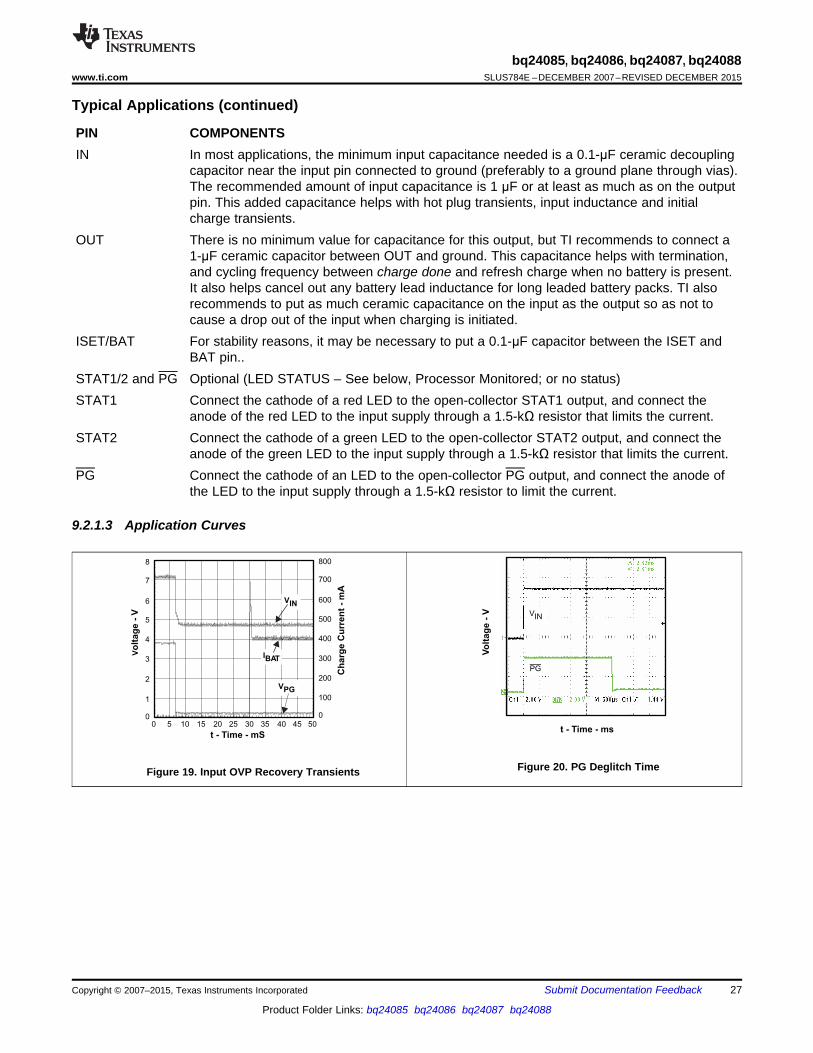
PIN COMPONENTSIN In most applications, the minimum input capacitance needed is a 0.1-μF ceramic decoupling
capacitor near the input pin connected to ground (preferably to a ground plane through vias).The recommended amount of input capacitance is 1 μF or at least as much as on the outputpin. This added capacitance helps with hot plug transients, input inductance and initialcharge transients.
OUT There is no minimum value for capacitance for this output, but TI recommends to connect a1-μF ceramic capacitor between OUT and ground. This capacitance helps with termination,and cycling frequency between charge done and refresh charge when no battery is present.It also helps cancel out any battery lead inductance for long leaded battery packs. TI alsorecommends to put as much ceramic capacitance on the input as the output so as not tocause a drop out of the input when charging is initiated.
ISET/BAT For stability reasons, it may be necessary to put a 0.1-μF capacitor between the ISET andBAT pin..
STAT1/2 and PG Optional (LED STATUS – See below, Processor Monitored; or no status)STAT1 Connect the cathode of a red LED to the open-collector STAT1 output, and connect the
anode of the red LED to the input supply through a 1.5-kΩ resistor that limits the current.STAT2 Connect the cathode of a green LED to the open-collector STAT2 output, and connect the
anode of the green LED to the input supply through a 1.5-kΩ resistor that limits the current.PG Connect the cathode of an LED to the open-collector PG output, and connect the anode of
the LED to the input supply through a 1.5-kΩ resistor to limit the current.
9.2.1.3 Application Curves
Figure 20. PG Deglitch TimeFigure 19. Input OVP Recovery Transients
Copyright © 2007–2015, Texas Instruments Incorporated Submit Documentation Feedback 27
Product Folder Links: bq24085 bq24086 bq24087 bq24088

IN
STAT1 TE
OUT
Li-Ion or Li-Pol
Battery Pack
+
Pack-
Pack+
STAT2
Vss ISET
CE
RED
GREEN
RSET
TMR
RTMR
1
2
3
4
5 6
7
8
9
10
BAT
Charge andTermination Enable
Input Power
R2
1.5 kW
R1
1.5 kW
bq24087
1 FmC2
49.9 kW
1.13 kW
C3
4.7 Fm
IN
STAT1 CE
OUT
Li-Ion or Li-Pol
Battery Pack
+
Pack-
Pack+
STAT2
Vss ISET
PG
RED
GREEN
RSET
TMR
RTMR
1
2
3
4
5 6
7
8
9
10
BAT
Charge Enable
and Power Good
Input Power
R2
1.5 kW
R1
1.5 kW
bq24085
1 FmC2
49.9 kW
1.13 kW
C3
4.7 Fm
bq24085, bq24086, bq24087, bq24088SLUS784E –DECEMBER 2007–REVISED DECEMBER 2015 www.ti.com
Typical Applications (continued)9.2.2 bq24085 Typical ApplicationFigure 21 illustrates the typical application circuit for bq24085.
Figure 21. bq24085 Application Schematic
9.2.2.1 Design RequirementsFollow the design requirements in bq24086 and bq24088 Typical Application.
9.2.3 bq24087 Typical ApplicationFigure 22 shows the typical application circuit for bq24087.
Figure 22. bq24087 Application Schematic
9.2.3.1 Design RequirementsFollow the design requirements in bq24086 and bq24088 Typical Application.
28 Submit Documentation Feedback Copyright © 2007–2015, Texas Instruments Incorporated
Product Folder Links: bq24085 bq24086 bq24087 bq24088

Needs to be sizedproperly COUT/BAT
GNDCIN
bq24085, bq24086, bq24087, bq24088www.ti.com SLUS784E –DECEMBER 2007–REVISED DECEMBER 2015
10 Power Supply RecommendationsThe devices are designed to operate from an input voltage supply range between 3.5 V and 6.5 V and currentcapability of at least the maximum designed charge current. This input supply should be well regulated. If locatedmore than a few inches from the bq24085/6/7/8 IN and GND terminals, a larger capacitor is recommended.
11 Layout
11.1 Layout GuidelinesIt is important to pay special attention to the PCB layout. The following provides some guidelines:• To obtain optimal performance, the decoupling capacitor from IN to GND (thermal pad) and the output filter
capacitors from OUT to GND (thermal pad) should be placed as close as possible to the bq2408x, with shorttrace runs to both IN, OUT and GND (thermal pad).
• All low-current GND connections should be kept separate from the high-current charge or discharge pathsfrom the battery. Use a single-point ground technique incorporating both the small signal ground path and thepower ground path.
• The high current charge paths into IN pin and from the OUT pin must be sized appropriately for the maximumcharge current in order to avoid voltage drops in these traces.
• The bq2408x family are packaged in a thermally enhanced MLP package. The package includes a thermalpad to provide an effective thermal contact between the IC and the printed circuit board (PCB); this thermalpad is also the main ground connection for the device. Connect the thermal pad to the PCB groundconnection. Full PCB design guidelines for this package are provided in the application note entitled:QFN/SON PCB Attachment Application Note, SLUA271.
11.2 Layout Example
Figure 23. bq2408x PCB Layout
Copyright © 2007–2015, Texas Instruments Incorporated Submit Documentation Feedback 29
Product Folder Links: bq24085 bq24086 bq24087 bq24088

T - TJ A=(JA)P
q
bq24085, bq24086, bq24087, bq24088SLUS784E –DECEMBER 2007–REVISED DECEMBER 2015 www.ti.com
11.3 Thermal ConsiderationsThe bq2408x family is packaged in a thermally enhanced MLP package. The package includes a thermal pad toprovide an effective thermal contact between the IC and the printed circuit board (PCB). Full PCB designguidelines for this package are provided in the application note entitled: QFN/SON PCB Attachment ApplicationNote, SLUA271.
The most common measure of package thermal performance is thermal impedance (θJA ) measured (ormodeled) from the chip junction to the air surrounding the package surface (ambient). Use Equation 13 as themathematical expression for θJA:
where• TJ = chip junction temperature• TA = ambient temperature• P = device power dissipation (13)
Factors that can greatly influence the measurement and calculation of θJA include:• Whether or not the device is board mounted• Trace size, composition, thickness, and geometry• Orientation of the device (horizontal or vertical)• Volume of the ambient air surrounding the device under test and airflow• Whether other surfaces are in close proximity to the device being tested
The device power dissipation, P, is a function of the charge rate and the voltage drop across the internalPowerFET. Use Equation 14 to calculate the device power dissipation when a battery pack is being charged:
P = [V(IN) – V(OUT)] × I(OUT) (14)
Due to the charge profile of Li-Ion batteries the maximum power dissipation is typically seen at the beginning ofthe charge cycle when the battery voltage is at its lowest. See the charging profile, Figure 8.
If the board thermal design is not adequate the programmed fast charge rate current may not be achieved undermaximum input voltage and minimum battery voltage, as the thermal loop can be active effectively reducing thecharge current to avoid excessive IC junction temperature.
30 Submit Documentation Feedback Copyright © 2007–2015, Texas Instruments Incorporated
Product Folder Links: bq24085 bq24086 bq24087 bq24088

bq24085, bq24086, bq24087, bq24088www.ti.com SLUS784E –DECEMBER 2007–REVISED DECEMBER 2015
12 Device and Documentation Support
12.1 Documentation Support
12.1.1 Related DocumentationFor related documentation see the following:
User's Guide, bq24085/6/7/8 Evaluation Module, SLUU305
12.2 Related LinksThe table below lists quick access links. Categories include technical documents, support and communityresources, tools and software, and quick access to sample or buy.
Table 9. Related LinksTECHNICAL TOOLS & SUPPORT &PARTS PRODUCT FOLDER SAMPLE & BUY DOCUMENTS SOFTWARE COMMUNITY
bq24085 Click here Click here Click here Click here Click herebq24086 Click here Click here Click here Click here Click herebq24087 Click here Click here Click here Click here Click herebq24088 Click here Click here Click here Click here Click here
12.3 Community ResourcesThe following links connect to TI community resources. Linked contents are provided "AS IS" by the respectivecontributors. They do not constitute TI specifications and do not necessarily reflect TI's views; see TI's Terms ofUse.
TI E2E™ Online Community TI's Engineer-to-Engineer (E2E) Community. Created to foster collaborationamong engineers. At e2e.ti.com, you can ask questions, share knowledge, explore ideas and helpsolve problems with fellow engineers.
Design Support TI's Design Support Quickly find helpful E2E forums along with design support tools andcontact information for technical support.
12.4 TrademarksE2E is a trademark of Texas Instruments.All other trademarks are the property of their respective owners.
12.5 Electrostatic Discharge CautionThese devices have limited built-in ESD protection. The leads should be shorted together or the device placed in conductive foamduring storage or handling to prevent electrostatic damage to the MOS gates.
12.6 GlossarySLYZ022 — TI Glossary.
This glossary lists and explains terms, acronyms, and definitions.
13 Mechanical, Packaging, and Orderable InformationThe following pages include mechanical, packaging, and orderable information. This information is the mostcurrent data available for the designated devices. This data is subject to change without notice and revision ofthis document. For browser-based versions of this data sheet, refer to the left-hand navigation.
Copyright © 2007–2015, Texas Instruments Incorporated Submit Documentation Feedback 31
Product Folder Links: bq24085 bq24086 bq24087 bq24088

PACKAGE OPTION ADDENDUM
www.ti.com 22-Jul-2017
Addendum-Page 1
PACKAGING INFORMATION
Orderable Device Status(1)
Package Type PackageDrawing
Pins PackageQty
Eco Plan(2)
Lead/Ball Finish(6)
MSL Peak Temp(3)
Op Temp (°C) Device Marking(4/5)
Samples
BQ24085DRCR ACTIVE VSON DRC 10 3000 Green (RoHS& no Sb/Br)
CU NIPDAU | Call TI Level-2-260C-1 YEAR 0 to 125 CDV
BQ24085DRCT ACTIVE VSON DRC 10 250 Green (RoHS& no Sb/Br)
CU NIPDAU | Call TI Level-2-260C-1 YEAR 0 to 125 CDV
BQ24085DRCTG4 ACTIVE VSON DRC 10 250 Green (RoHS& no Sb/Br)
CU NIPDAU Level-2-260C-1 YEAR 0 to 125 CDV
BQ24086DRCR ACTIVE VSON DRC 10 3000 Green (RoHS& no Sb/Br)
CU NIPDAU Level-2-260C-1 YEAR 0 to 125 CDW
BQ24086DRCT ACTIVE VSON DRC 10 250 Green (RoHS& no Sb/Br)
CU NIPDAU Level-2-260C-1 YEAR 0 to 125 CDW
BQ24087DRCR ACTIVE VSON DRC 10 3000 Green (RoHS& no Sb/Br)
CU NIPDAU Level-2-260C-1 YEAR 0 to 125 CDX
BQ24087DRCT ACTIVE VSON DRC 10 250 Green (RoHS& no Sb/Br)
CU NIPDAU Level-2-260C-1 YEAR 0 to 125 CDX
BQ24088DRCR ACTIVE VSON DRC 10 3000 Green (RoHS& no Sb/Br)
CU NIPDAU Level-2-260C-1 YEAR 0 to 125 CHE
BQ24088DRCT ACTIVE VSON DRC 10 250 Green (RoHS& no Sb/Br)
CU NIPDAU Level-2-260C-1 YEAR 0 to 125 CHE
HPA00614DRCR ACTIVE VSON DRC 10 3000 Green (RoHS& no Sb/Br)
CU NIPDAU Level-2-260C-1 YEAR 0 to 125 CDV
(1) The marketing status values are defined as follows:ACTIVE: Product device recommended for new designs.LIFEBUY: TI has announced that the device will be discontinued, and a lifetime-buy period is in effect.NRND: Not recommended for new designs. Device is in production to support existing customers, but TI does not recommend using this part in a new design.PREVIEW: Device has been announced but is not in production. Samples may or may not be available.OBSOLETE: TI has discontinued the production of the device.
(2) RoHS: TI defines "RoHS" to mean semiconductor products that are compliant with the current EU RoHS requirements for all 10 RoHS substances, including the requirement that RoHS substancedo not exceed 0.1% by weight in homogeneous materials. Where designed to be soldered at high temperatures, "RoHS" products are suitable for use in specified lead-free processes. TI mayreference these types of products as "Pb-Free".RoHS Exempt: TI defines "RoHS Exempt" to mean products that contain lead but are compliant with EU RoHS pursuant to a specific EU RoHS exemption.Green: TI defines "Green" to mean the content of Chlorine (Cl) and Bromine (Br) based flame retardants meet JS709B low halogen requirements of <=1000ppm threshold. Antimony trioxide basedflame retardants must also meet the <=1000ppm threshold requirement.
(3) MSL, Peak Temp. - The Moisture Sensitivity Level rating according to the JEDEC industry standard classifications, and peak solder temperature.

PACKAGE OPTION ADDENDUM
www.ti.com 22-Jul-2017
Addendum-Page 2
(4) There may be additional marking, which relates to the logo, the lot trace code information, or the environmental category on the device.
(5) Multiple Device Markings will be inside parentheses. Only one Device Marking contained in parentheses and separated by a "~" will appear on a device. If a line is indented then it is a continuationof the previous line and the two combined represent the entire Device Marking for that device.
(6) Lead/Ball Finish - Orderable Devices may have multiple material finish options. Finish options are separated by a vertical ruled line. Lead/Ball Finish values may wrap to two lines if the finishvalue exceeds the maximum column width.
Important Information and Disclaimer:The information provided on this page represents TI's knowledge and belief as of the date that it is provided. TI bases its knowledge and belief on informationprovided by third parties, and makes no representation or warranty as to the accuracy of such information. Efforts are underway to better integrate information from third parties. TI has taken andcontinues to take reasonable steps to provide representative and accurate information but may not have conducted destructive testing or chemical analysis on incoming materials and chemicals.TI and TI suppliers consider certain information to be proprietary, and thus CAS numbers and other limited information may not be available for release.
In no event shall TI's liability arising out of such information exceed the total purchase price of the TI part(s) at issue in this document sold by TI to Customer on an annual basis.

TAPE AND REEL INFORMATION
*All dimensions are nominal
Device PackageType
PackageDrawing
Pins SPQ ReelDiameter
(mm)
ReelWidth
W1 (mm)
A0(mm)
B0(mm)
K0(mm)
P1(mm)
W(mm)
Pin1Quadrant
BQ24085DRCR VSON DRC 10 3000 330.0 12.4 3.3 3.3 1.1 8.0 12.0 Q2
BQ24085DRCR VSON DRC 10 3000 330.0 12.4 3.3 3.3 1.1 8.0 12.0 Q2
BQ24085DRCT VSON DRC 10 250 180.0 12.4 3.3 3.3 1.1 8.0 12.0 Q2
BQ24085DRCT VSON DRC 10 250 180.0 12.5 3.3 3.3 1.1 8.0 12.0 Q2
BQ24086DRCR VSON DRC 10 3000 330.0 12.4 3.3 3.3 1.1 8.0 12.0 Q2
BQ24086DRCR VSON DRC 10 3000 330.0 12.4 3.3 3.3 1.1 8.0 12.0 Q2
BQ24086DRCT VSON DRC 10 250 180.0 12.5 3.3 3.3 1.1 8.0 12.0 Q2
BQ24086DRCT VSON DRC 10 250 180.0 12.4 3.3 3.3 1.1 8.0 12.0 Q2
BQ24087DRCR VSON DRC 10 3000 330.0 12.4 3.3 3.3 1.1 8.0 12.0 Q2
BQ24087DRCT VSON DRC 10 250 180.0 12.4 3.3 3.3 1.1 8.0 12.0 Q2
BQ24088DRCR VSON DRC 10 3000 330.0 12.4 3.3 3.3 1.1 8.0 12.0 Q2
BQ24088DRCT VSON DRC 10 250 180.0 12.4 3.3 3.3 1.1 8.0 12.0 Q2
PACKAGE MATERIALS INFORMATION
www.ti.com 3-Aug-2017
Pack Materials-Page 1

*All dimensions are nominal
Device Package Type Package Drawing Pins SPQ Length (mm) Width (mm) Height (mm)
BQ24085DRCR VSON DRC 10 3000 338.0 355.0 50.0
BQ24085DRCR VSON DRC 10 3000 367.0 367.0 35.0
BQ24085DRCT VSON DRC 10 250 210.0 185.0 35.0
BQ24085DRCT VSON DRC 10 250 205.0 200.0 33.0
BQ24086DRCR VSON DRC 10 3000 338.0 355.0 50.0
BQ24086DRCR VSON DRC 10 3000 367.0 367.0 35.0
BQ24086DRCT VSON DRC 10 250 338.0 355.0 50.0
BQ24086DRCT VSON DRC 10 250 210.0 185.0 35.0
BQ24087DRCR VSON DRC 10 3000 367.0 367.0 35.0
BQ24087DRCT VSON DRC 10 250 210.0 185.0 35.0
BQ24088DRCR VSON DRC 10 3000 367.0 367.0 35.0
BQ24088DRCT VSON DRC 10 250 210.0 185.0 35.0
PACKAGE MATERIALS INFORMATION
www.ti.com 3-Aug-2017
Pack Materials-Page 2

GENERIC PACKAGE VIEW
Images above are just a representation of the package family, actual package may vary.Refer to the product data sheet for package details.
DRC 10 VSON - 1 mm max heightPLASTIC SMALL OUTLINE - NO LEAD
4204102-3/M

www.ti.com
PACKAGE OUTLINE
C
10X 0.300.18
2.4 0.1
2X2
1.65 0.1
8X 0.5
1 MAX
10X 0.50.3
0.050.00
A 3.12.9
B
3.12.9
(0.2) TYP4X (0.25)
2X (0.5)
VSON - 1 mm max heightDRC0010JPLASTIC SMALL OUTLINE - NO LEAD
4218878/A 09/2017
PIN 1 INDEX AREA
SEATING PLANE
0.08 C
1
56
10
(OPTIONAL)PIN 1 ID 0.1 C A B
0.05 C
THERMAL PADEXPOSED
SYMM
SYMM11
NOTES: 1. All linear dimensions are in millimeters. Any dimensions in parenthesis are for reference only. Dimensioning and tolerancing per ASME Y14.5M. 2. This drawing is subject to change without notice. 3. The package thermal pad must be soldered to the printed circuit board for optimal thermal and mechanical performance.
SCALE 4.000

www.ti.com
EXAMPLE BOARD LAYOUT
0.07 MINALL AROUND
10X (0.25)
(2.4)
(2.8)
8X (0.5)
(1.65)
( 0.2) VIATYP
(0.575)
(0.95)
10X (0.6)
(R0.05) TYP
(3.4)
4X (0.25)
(0.5)
VSON - 1 mm max heightDRC0010JPLASTIC SMALL OUTLINE - NO LEAD
4218878/A 09/2017
SYMM
1
5 6
10
LAND PATTERN EXAMPLEEXPOSED METAL SHOWN
SCALE:20X
11SYMM
METAL UNDERSOLDER MASK
SOLDER MASKOPENING
NOTES: (continued) 4. This package is designed to be soldered to a thermal pad on the board. For more information, see Texas Instruments literature number SLUA271 (www.ti.com/lit/slua271).5. Vias are optional depending on application, refer to device data sheet. If any vias are implemented, refer to their locations shown on this view. It is recommended that vias under paste be filled, plugged or tented.

www.ti.com
EXAMPLE STENCIL DESIGN
(R0.05) TYP
10X (0.25)
10X (0.6)
2X (1.5)
2X(1.06)
(2.8)
(0.63)
8X (0.5)
(0.5)
4X (0.34)
4X (0.25)
(1.53)
VSON - 1 mm max heightDRC0010JPLASTIC SMALL OUTLINE - NO LEAD
4218878/A 09/2017
NOTES: (continued) 6. Laser cutting apertures with trapezoidal walls and rounded corners may offer better paste release. IPC-7525 may have alternate design recommendations.
SOLDER PASTE EXAMPLEBASED ON 0.125 mm THICK STENCIL
EXPOSED PAD 11:
80% PRINTED SOLDER COVERAGE BY AREASCALE:25X
SYMM
1
56
10
EXPOSED METALTYP
11
SYMM
SOLDER MASK OPENING
METAL UNDERSOLDER MASK

www.ti.com
PACKAGE OUTLINE
C
TYP10.639.97
2.65 MAX
18X 1.27
20X 0.510.31
2X11.43
TYP0.330.10
0 - 80.30.1
0.25GAGE PLANE
1.270.40
A
NOTE 3
13.012.6
B 7.67.4
4220724/A 05/2016
SOIC - 2.65 mm max heightDW0020ASOIC
NOTES: 1. All linear dimensions are in millimeters. Dimensions in parenthesis are for reference only. Dimensioning and tolerancing per ASME Y14.5M. 2. This drawing is subject to change without notice. 3. This dimension does not include mold flash, protrusions, or gate burrs. Mold flash, protrusions, or gate burrs shall not exceed 0.15 mm per side. 4. This dimension does not include interlead flash. Interlead flash shall not exceed 0.43 mm per side.5. Reference JEDEC registration MS-013.
120
0.25 C A B
1110
PIN 1 IDAREA
NOTE 4
SEATING PLANE
0.1 C
SEE DETAIL A
DETAIL ATYPICAL
SCALE 1.200

www.ti.com
EXAMPLE BOARD LAYOUT
(9.3)
0.07 MAXALL AROUND
0.07 MINALL AROUND
20X (2)
20X (0.6)
18X (1.27)
(R )TYP
0.05
4220724/A 05/2016
SOIC - 2.65 mm max heightDW0020ASOIC
SYMM
SYMM
LAND PATTERN EXAMPLESCALE:6X
1
10 11
20
NOTES: (continued) 6. Publication IPC-7351 may have alternate designs. 7. Solder mask tolerances between and around signal pads can vary based on board fabrication site.
METALSOLDER MASKOPENING
NON SOLDER MASKDEFINED
SOLDER MASK DETAILS
SOLDER MASKOPENING
METAL UNDERSOLDER MASK
SOLDER MASKDEFINED

www.ti.com
EXAMPLE STENCIL DESIGN
(9.3)
18X (1.27)
20X (0.6)
20X (2)
4220724/A 05/2016
SOIC - 2.65 mm max heightDW0020ASOIC
NOTES: (continued) 8. Laser cutting apertures with trapezoidal walls and rounded corners may offer better paste release. IPC-7525 may have alternate design recommendations. 9. Board assembly site may have different recommendations for stencil design.
SYMM
SYMM
1
10 11
20
SOLDER PASTE EXAMPLEBASED ON 0.125 mm THICK STENCIL
SCALE:6X

IMPORTANT NOTICE
Texas Instruments Incorporated (TI) reserves the right to make corrections, enhancements, improvements and other changes to itssemiconductor products and services per JESD46, latest issue, and to discontinue any product or service per JESD48, latest issue. Buyersshould obtain the latest relevant information before placing orders and should verify that such information is current and complete.TI’s published terms of sale for semiconductor products (http://www.ti.com/sc/docs/stdterms.htm) apply to the sale of packaged integratedcircuit products that TI has qualified and released to market. Additional terms may apply to the use or sale of other types of TI products andservices.Reproduction of significant portions of TI information in TI data sheets is permissible only if reproduction is without alteration and isaccompanied by all associated warranties, conditions, limitations, and notices. TI is not responsible or liable for such reproduceddocumentation. Information of third parties may be subject to additional restrictions. Resale of TI products or services with statementsdifferent from or beyond the parameters stated by TI for that product or service voids all express and any implied warranties for theassociated TI product or service and is an unfair and deceptive business practice. TI is not responsible or liable for any such statements.Buyers and others who are developing systems that incorporate TI products (collectively, “Designers”) understand and agree that Designersremain responsible for using their independent analysis, evaluation and judgment in designing their applications and that Designers havefull and exclusive responsibility to assure the safety of Designers' applications and compliance of their applications (and of all TI productsused in or for Designers’ applications) with all applicable regulations, laws and other applicable requirements. Designer represents that, withrespect to their applications, Designer has all the necessary expertise to create and implement safeguards that (1) anticipate dangerousconsequences of failures, (2) monitor failures and their consequences, and (3) lessen the likelihood of failures that might cause harm andtake appropriate actions. Designer agrees that prior to using or distributing any applications that include TI products, Designer willthoroughly test such applications and the functionality of such TI products as used in such applications.TI’s provision of technical, application or other design advice, quality characterization, reliability data or other services or information,including, but not limited to, reference designs and materials relating to evaluation modules, (collectively, “TI Resources”) are intended toassist designers who are developing applications that incorporate TI products; by downloading, accessing or using TI Resources in anyway, Designer (individually or, if Designer is acting on behalf of a company, Designer’s company) agrees to use any particular TI Resourcesolely for this purpose and subject to the terms of this Notice.TI’s provision of TI Resources does not expand or otherwise alter TI’s applicable published warranties or warranty disclaimers for TIproducts, and no additional obligations or liabilities arise from TI providing such TI Resources. TI reserves the right to make corrections,enhancements, improvements and other changes to its TI Resources. TI has not conducted any testing other than that specificallydescribed in the published documentation for a particular TI Resource.Designer is authorized to use, copy and modify any individual TI Resource only in connection with the development of applications thatinclude the TI product(s) identified in such TI Resource. NO OTHER LICENSE, EXPRESS OR IMPLIED, BY ESTOPPEL OR OTHERWISETO ANY OTHER TI INTELLECTUAL PROPERTY RIGHT, AND NO LICENSE TO ANY TECHNOLOGY OR INTELLECTUAL PROPERTYRIGHT OF TI OR ANY THIRD PARTY IS GRANTED HEREIN, including but not limited to any patent right, copyright, mask work right, orother intellectual property right relating to any combination, machine, or process in which TI products or services are used. Informationregarding or referencing third-party products or services does not constitute a license to use such products or services, or a warranty orendorsement thereof. Use of TI Resources may require a license from a third party under the patents or other intellectual property of thethird party, or a license from TI under the patents or other intellectual property of TI.TI RESOURCES ARE PROVIDED “AS IS” AND WITH ALL FAULTS. TI DISCLAIMS ALL OTHER WARRANTIES ORREPRESENTATIONS, EXPRESS OR IMPLIED, REGARDING RESOURCES OR USE THEREOF, INCLUDING BUT NOT LIMITED TOACCURACY OR COMPLETENESS, TITLE, ANY EPIDEMIC FAILURE WARRANTY AND ANY IMPLIED WARRANTIES OFMERCHANTABILITY, FITNESS FOR A PARTICULAR PURPOSE, AND NON-INFRINGEMENT OF ANY THIRD PARTY INTELLECTUALPROPERTY RIGHTS. TI SHALL NOT BE LIABLE FOR AND SHALL NOT DEFEND OR INDEMNIFY DESIGNER AGAINST ANY CLAIM,INCLUDING BUT NOT LIMITED TO ANY INFRINGEMENT CLAIM THAT RELATES TO OR IS BASED ON ANY COMBINATION OFPRODUCTS EVEN IF DESCRIBED IN TI RESOURCES OR OTHERWISE. IN NO EVENT SHALL TI BE LIABLE FOR ANY ACTUAL,DIRECT, SPECIAL, COLLATERAL, INDIRECT, PUNITIVE, INCIDENTAL, CONSEQUENTIAL OR EXEMPLARY DAMAGES INCONNECTION WITH OR ARISING OUT OF TI RESOURCES OR USE THEREOF, AND REGARDLESS OF WHETHER TI HAS BEENADVISED OF THE POSSIBILITY OF SUCH DAMAGES.Unless TI has explicitly designated an individual product as meeting the requirements of a particular industry standard (e.g., ISO/TS 16949and ISO 26262), TI is not responsible for any failure to meet such industry standard requirements.Where TI specifically promotes products as facilitating functional safety or as compliant with industry functional safety standards, suchproducts are intended to help enable customers to design and create their own applications that meet applicable functional safety standardsand requirements. Using products in an application does not by itself establish any safety features in the application. Designers mustensure compliance with safety-related requirements and standards applicable to their applications. Designer may not use any TI products inlife-critical medical equipment unless authorized officers of the parties have executed a special contract specifically governing such use.Life-critical medical equipment is medical equipment where failure of such equipment would cause serious bodily injury or death (e.g., lifesupport, pacemakers, defibrillators, heart pumps, neurostimulators, and implantables). Such equipment includes, without limitation, allmedical devices identified by the U.S. Food and Drug Administration as Class III devices and equivalent classifications outside the U.S.TI may expressly designate certain products as completing a particular qualification (e.g., Q100, Military Grade, or Enhanced Product).Designers agree that it has the necessary expertise to select the product with the appropriate qualification designation for their applicationsand that proper product selection is at Designers’ own risk. Designers are solely responsible for compliance with all legal and regulatoryrequirements in connection with such selection.Designer will fully indemnify TI and its representatives against any damages, costs, losses, and/or liabilities arising out of Designer’s non-compliance with the terms and provisions of this Notice.
Mailing Address: Texas Instruments, Post Office Box 655303, Dallas, Texas 75265Copyright © 2018, Texas Instruments Incorporated