Embed Size (px)
Citation preview
- 1 -
Rev. 1.0, Oct. 2011
SAMSUNG ELECTRONICS RESERVES THE RIGHT TO CHANGE PRODUCTS, INFORMATION AND SPECIFICATIONS WITHOUT NOTICE.
Products and specifications discussed herein are for reference purposes only. All information discussed herein is provided on an "AS IS" basis, without warranties of any kind.
This document and all information discussed herein remain the sole and exclusive property of Samsung Electronics. No license of any patent, copyright, mask work, trademark or any other intellectual property right is granted by one party to the other party under this document, by implication, estoppel or other-wise.
Samsung products are not intended for use in life support, critical care, medical, safety equipment, or similar applications where product failure could result in loss of life or personal or physical harm, or any military or defense application, or any governmental procurement to which special terms or provisions may apply.
For updates or additional information about Samsung products, contact your nearest Samsung office.
All brand names, trademarks and registered trademarks belong to their respective owners.
ⓒ 2011 Samsung Electronics Co., Ltd. All rights reserved.
MZ5EA100HMDR-00003MZ5EA200HMDR-00003MZ5EA400HMFP-00003
SM825 2.5"SATA 3.0Gb/s E-MLC SSD(NAND based Solid State Drive)
datasheet
- 2 -
MZ5EA400HMFP-00003 SSD Rev. 1.0
MZ5EA200HMDR-00003 datasheetMZ5EA100HMDR-00003
Revision HistoryRevision No. History Draft Date Remark Editor
1.0 Final version Oct.20.2011 Final Ryder Kim
- 3 -
MZ5EA400HMFP-00003 SSD Rev. 1.0
MZ5EA200HMDR-00003 datasheetMZ5EA100HMDR-00003
Table Of Contents
1.0 Introduction ................................................................................................................................................................ 51.1 General Description................................................................................................................................................. 51.2 Block Diagram ......................................................................................................................................................... 5
2.0 Product Specification .................................................................................................................................................62.1 Interface and Configuration .................................................................................................................................... 62.2 System Performance .............................................................................................................................................. 6
2.2.1 Sequential Read and Write Bandwidth ............................................................................................................ 62.2.2 Random Read and Write IOPS (Input and Output operation Per Second) ...................................................... 6
2.3 Drive Capacity ........................................................................................................................................................ 62.4 Supply Voltage ....................................................................................................................................................... 62.5 Power Consumption ............................................................................................................................................... 72.6 Reliability ................................................................................................................................................................ 72.7 Environmental Specification ................................................................................................................................... 7
2.7.1 Temperature..................................................................................................................................................... 72.7.2 Shock and Vibration ......................................................................................................................................... 72.7.3 Altitude ............................................................................................................................................................ 8
3.0 Physical Specification ................................................................................................................................................ 83.1 Physical Dimension and Weight ............................................................................................................................. 83.2 Case Outline........................................................................................................................................................... 8
4.0 Electrical Interface Specification ................................................................................................................................ 94.1 Serial ATA Interface Connector.............................................................................................................................. 9
4.1.1 Drive Connector Model : Amphenol, SATA00 100941T................................................................................... 94.1.2 Connector Dimension and Pin Location........................................................................................................... 9
4.2 Pin Assignments and Definition.............................................................................................................................. 10
5.0 Command Descriptions..............................................................................................................................................115.1 Supported ATA Commands.................................................................................................................................... 115.2 SECURITY FEATURE Set ..................................................................................................................................... 12
5.2.1 SECURITY mode default setting...................................................................................................................... 125.2.2 Initial setting of the user password................................................................................................................... 125.2.3 SECURITY mode operation from power-on..................................................................................................... 125.2.4 Password lost................................................................................................................................................... 12
5.3 SMART FEATURE Set (B0h) ................................................................................................................................. 125.3.1 Sub Command ................................................................................................................................................. 12
5.3.1.1 S.M.A.R.T. Read Attribute Values (subcommand D0h)l ............................................................................ 125.3.1.2 S.M.A.R.T. Read Attribute Thresholds (subcommand D1h) ...................................................................... 125.3.1.3 S.M.A.R.T. Enable/Disable Attribute Autosave (subcommand D2h) ......................................................... 135.3.1.4 S.M.A.R.T. Save Attribute Values (subcommand D3h) ............................................................................. 135.3.1.5 S.M.A.R.T. Execute Off-line Immediate (subcommand D4h) .................................................................... 135.3.1.6 S.M.A.R.T. Read Log Sector (subcommand D5h)..................................................................................... 145.3.1.7 S.M.A.R.T. Write Log Sector (subcommand D6h)..................................................................................... 145.3.1.8 S.M.A.R.T. Enable Operations (subcommand D8h).................................................................................. 145.3.1.9 S.M.A.R.T. Disable Operations (subcommand D9h) ................................................................................. 145.3.1.10 S.M.A.R.T. Return Status (subcommand DAh) ....................................................................................... 15
5.3.2 Device Attribute Data Structure........................................................................................................................ 155.3.2.1 Data Structure Revision Number ............................................................................................................... 155.3.2.2 Individual Attribute Data Structure ............................................................................................................. 165.3.2.3 Off-Line Data Collection Status ................................................................................................................. 175.3.2.4 Self-test execution status........................................................................................................................... 175.3.2.5 Total time in seconds to complete off-line data collection activity ............................................................. 175.3.2.6 Current segment pointer ............................................................................................................................ 175.3.2.7 Off-line data collection capability ............................................................................................................... 175.3.2.8 S.M.A.R.T. Capability ................................................................................................................................ 185.3.2.9 Error logging capability .............................................................................................................................. 185.3.2.10 Self-test failure check point...................................................................................................................... 185.3.2.11 Self-test completion time ......................................................................................................................... 185.3.2.12 Data Structure Checksum........................................................................................................................ 18
5.3.3 Device Attribute Thresholds data structure ..................................................................................................... 185.3.3.1 Data Structure Revision Number ............................................................................................................... 18
- 4 -
MZ5EA400HMFP-00003 SSD Rev. 1.0
MZ5EA200HMDR-00003 datasheetMZ5EA100HMDR-00003
5.3.3.2 Individual Thresholds Data Structure......................................................................................................... 195.3.3.3 Attribute ID Numbers ................................................................................................................................. 195.3.3.4 Attribute Threshold .................................................................................................................................... 195.3.3.5 Data Structure Checksum.......................................................................................................................... 19
5.3.4 S.M.A.R.T. Log Directory ................................................................................................................................. 195.3.5 S.M.A.R.T. error log sector .............................................................................................................................. 20
5.3.5.1 S.M.A.R.T. error log version ...................................................................................................................... 205.3.5.2 Error log pointer ......................................................................................................................................... 205.3.5.3 Device error count ..................................................................................................................................... 205.3.5.4 Error log data structure .............................................................................................................................. 205.3.5.5 Command data structure ........................................................................................................................... 215.3.5.6 Error data structure.................................................................................................................................... 21
5.3.6 Self-test log structure ....................................................................................................................................... 225.3.7 Selective self-test log data structure ................................................................................................................ 225.3.8 Error reporting .................................................................................................................................................. 23
6.0 SPOR Specification (Sudden Power Off and Recovery) ........................................................................................... 236.1 Data Recovery in Sudden Power Off...................................................................................................................... 236.2 Time to Ready Sequence ....................................................................................................................................... 236.3 Treatment Specification.......................................................................................................................................... 23
7.0 SATAII Optional Feature............................................................................................................................................247.1 Power Segment Pin P11 ........................................................................................................................................ 247.2 Activity LED indication ............................................................................................................................................ 247.3 Asynchronous Signal Recovery.............................................................................................................................. 24
8.0 OOB signaling and Phy Power State .........................................................................................................................258.1 OOB signaling ........................................................................................................................................................ 25
8.1.1 OOB signal spacing ......................................................................................................................................... 258.2 Phy Power State..................................................................................................................................................... 25
8.2.1 COMRESET sequence state diagram ............................................................................................................. 258.2.2 Interface Power States..................................................................................................................................... 25
8.2.2.1 PHYRDY.................................................................................................................................................... 258.2.2.2 Partial......................................................................................................................................................... 258.2.2.3 Slumber ..................................................................................................................................................... 25
8.2.3 Partial/Slumber to PHYRDY............................................................................................................................. 258.2.3.1 Host Initiated.............................................................................................................................................. 258.2.3.2 Device Initiated .......................................................................................................................................... 25
8.2.4 PHYRDY to Partial/Slumber............................................................................................................................. 258.2.4.1 Host Initiated for Partial ............................................................................................................................. 258.2.4.2 Device Initiated for Partial .......................................................................................................................... 25
9.0 Identify Device Data.................................................................................................................................................. 26
10.0 Ordering Information ................................................................................................................................................ 28
11.0 Product Line up........................................................................................................................................................ 28
- 5 -
MZ5EA400HMFP-00003 SSD Rev. 1.0
MZ5EA200HMDR-00003 datasheetMZ5EA100HMDR-00003
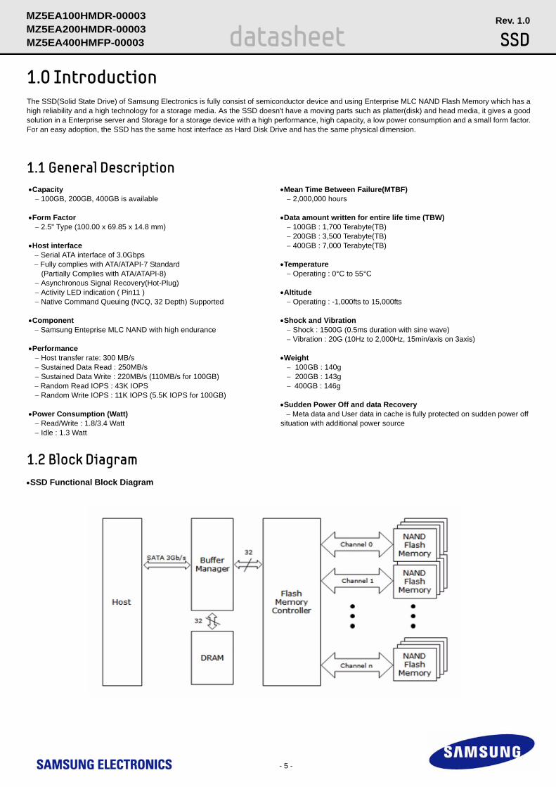
1.0 IntroductionThe SSD(Solid State Drive) of Samsung Electronics is fully consist of semiconductor device and using Enterprise MLC NAND Flash Memory which has a high reliability and a high technology for a storage media. As the SSD doesn't have a moving parts such as platter(disk) and head media, it gives a good solution in a Enterprise server and Storage for a storage device with a high performance, high capacity, a low power consumption and a small form factor. For an easy adoption, the SSD has the same host interface as Hard Disk Drive and has the same physical dimension.
1.1 General Description
1.2 Block Diagram•SSD Functional Block Diagram
•Capacity − 100GB, 200GB, 400GB is available
•Form Factor − 2.5" Type (100.00 x 69.85 x 14.8 mm) •Host interface − Serial ATA interface of 3.0Gbps − Fully complies with ATA/ATAPI-7 Standard (Partially Complies with ATA/ATAPI-8) − Asynchronous Signal Recovery(Hot-Plug) − Activity LED indication ( Pin11 ) − Native Command Queuing (NCQ, 32 Depth) Supported
•Component − Samsung Enteprise MLC NAND with high endurance
•Performance − Host transfer rate: 300 MB/s − Sustained Data Read : 250MB/s − Sustained Data Write : 220MB/s (110MB/s for 100GB) − Random Read IOPS : 43K IOPS − Random Write IOPS : 11K IOPS (5.5K IOPS for 100GB)
•Power Consumption (Watt) − Read/Write : 1.8/3.4 Watt − Idle : 1.3 Watt
•Mean Time Between Failure(MTBF) − 2,000,000 hours
•Data amount written for entire life time (TBW) − 100GB : 1,700 Terabyte(TB) − 200GB : 3,500 Terabyte(TB) − 400GB : 7,000 Terabyte(TB)
•Temperature − Operating : 0°C to 55°C
•Altitude − Operating : -1,000fts to 15,000fts
•Shock and Vibration − Shock : 1500G (0.5ms duration with sine wave) − Vibration : 20G (10Hz to 2,000Hz, 15min/axis on 3axis)
•Weight − 100GB : 140g − 200GB : 143g − 400GB : 146g
•Sudden Power Off and data Recovery − Meta data and User data in cache is fully protected on sudden power off situation with additional power source
- 6 -
MZ5EA400HMFP-00003 SSD Rev. 1.0
MZ5EA200HMDR-00003 datasheetMZ5EA100HMDR-00003
2.0 Product Specification
2.1 Interface and Configuration• Maximum Bandwidth : 300 MB/sec (3.0 Gb/sec).• PIO 0 to 4 mode• UDMA 0 to 6 mode (Ultra DMA133)• Fully compatible with ATA-7 Standard (Serial ATA Revision 2.6) (Partially Complies with ATA/ATAPI-8)
2.2 System Performance
2.2.1 Sequential Read and Write Bandwidth
NOTE : 1. Measured performance on IOMeter2. Data transfer size is 128KB and Queue depth is 32
2.2.2 Random Read and Write IOPS (Input and Output operation Per Second)
NOTE : 1. Measured performance on IOMETER2. Data transfer size is 4KB and Queue depth is 32
2.3 Drive Capacity
NOTE : 1. 1 Gigabyte(GB) = 1,000,000,000 Bytes2. 1 Sector = 512 Bytes
2.4 Supply Voltage
Bandwidth Type Performance
Sustained Sequential Read Bandwidth Up to 250 MB/s
Sustained Sequential Write Bandwidth Up to 220 MB/s
IOPS Type Performance
Sustained Random Read IOPS Up to 43,000 IOPS
Sustained Random Write IOPS Up to 11,000 IOPS
MZ5EA100HMDR MZ5EA200HMDR MZ5EA400HMFP
Unformatted Capacity 100 GB 200 GB 400 GB
User-Addressable Sectors 195,371,568 390,721,968 781,422,768
Item Requirements
Allowable voltage 5V + 5%12V + 5%
- 7 -
MZ5EA400HMFP-00003 SSD Rev. 1.0
MZ5EA200HMDR-00003 datasheetMZ5EA100HMDR-00003
2.5 Power Consumption
NOTE : 1. Measured power consumption under 100% 4KB random read/write operation
2.6 Reliability
NOTE : 1. TBW is TeraByte Written, that is, total data amount written for entire life time. 1 Terabyte = 1,000,000,000 Byte2. Above TBW is considered under data aligned condition to 8KB 3. Data retention is not under consideration on power-on state because SSD manages data retention by SSD itself4. MTBF is Mean Time Between Failure. As same word, annual failure ratio is 0.4%5. UBER is Uncorrectable Bit Error Ratio
2.7 Environmental Specification
2.7.1 Temperature
NOTE : 1. Temperature specification is following JEDEC standard; Expressed temperature must be measured right on the case2. Humidity is measured in non-condensing
2.7.2 Shock and Vibration
NOTE : 1. Test condition for shock : 0.5ms duration with sine wave2. Test condition for vibration : 10Hz to 2,000Hz, 15min/axis on 3axis
Power Typical(W)
Active Read 1.8
Active Write 3.4
Idle 1.3
MZ5EA100HMDR MZ5EA200HMDR MZ5EA400HMFP
TBW* 1,700 TB 3,500 TB 7,000 TB
Data Retention* 3 months
MTBF* 2,000,000 hours
UBER* 1 bit error in 10E17bits
MZ5EA100HMDR MZ5EA200HMDR MZ5EA400HMFP
Temperature (Operating) 0’C to 55’C
Temperature (Non-operating) -40’C to 85’C
Humidity 5% to 90%
MZ5EA100HMDR MZ5EA200HMDR MZ5EA400HMFP
Shock (Operating, Non-operating)
1500G
Vibration (Operating, Non-operating)
20G peak
- 8 -
MZ5EA400HMFP-00003 SSD Rev. 1.0
MZ5EA200HMDR-00003 datasheetMZ5EA100HMDR-00003
2.7.3 Altitude
NOTE : 1. Test condition for altitude : recurring sequential read and write for 6hours in each 5’C and 55’C at 15,000 fts
3.0 Physical Specification
3.1 Physical Dimension and Weight
3.2 Case Outline
MZ5EA100HMDR MZ5EA200HMDR MZ5EA400HMFP
Altitude (Operating) -1,000 fts to 15,000 fts
Altitude (Non-operating) -1,000 fts to 40,000 fts
Part No. Density Height(mm) Width(mm) Length(mm) Weight(gram)
MZ5EA100HMDR 100GB 14.80 ± 0.2 69.85 ± 0.25 100.00 ± 0.25 140g
MZ5EA200HMDR 200GB 14.80 ± 0.2 69.85 ± 0.25 100.00 ± 0.25 143g
MZ5EA400HMFP 400GB 14.80 ± 0.2 69.85 ± 0.25 100.00 ± 0.25 146g
- 9 -
MZ5EA400HMFP-00003 SSD Rev. 1.0
MZ5EA200HMDR-00003 datasheetMZ5EA100HMDR-00003
4.0 Electrical Interface Specification
4.1 Serial ATA Interface Connector
4.1.1 Drive Connector Model : Amphenol, SATA00 100941T
4.1.2 Connector Dimension and Pin Location
- 10 -
MZ5EA400HMFP-00003 SSD Rev. 1.0
MZ5EA200HMDR-00003 datasheetMZ5EA100HMDR-00003
4.2 Pin Assignments and Definition
NOTE : 1. 5V(P7, P8 and P9) and 12V(P13, P14 and P15) is used to supply power to the SSD. SSD may not work unless host put power to both 5V power pin and 12V power pin.2. 3.3V(P1, P2 and P3) is not used for this SSD. 3. The usage of power pin P11 is treated on ’SATA Optional Feature Chapter’
No. Plug Connector pin definition
Signal
S1 GND 2nd mate
S2 A+ Differential signal A from Phy
S3 A-
S4 GND 2nd mate
S5 B- Differential signal B from Phy
S6 B+
S7 GND 2nd mate
Key and spacing spearate signal and power segments
Power
P1 V33 3.3V power (Unused)
P2 V33 3.3V power (Unused)
P3 V33 3.3V power, pre-charge, 2nd mate (Unused)
P4 GND 1st mate
P5 GND 2nd mate
P6 GND 2nd mate
P7 V5 5V power, pre-charge, 2nd mate
P8 V5 5V power
P9 V5 5V power
P10 GND 2nd mate
P11 DAS/DSS Device Activity Signal
P12 GND 1st mate
P13 V12 12V power, pre-charge, 2nd mate
P14 V12 12V power
P15 V12 12V power
- 11 -
MZ5EA400HMFP-00003 SSD Rev. 1.0
MZ5EA200HMDR-00003 datasheetMZ5EA100HMDR-00003
5.0 Command Descriptions
5.1 Supported ATA Commands
Command Name Command Code (Hex) Command Name Command Code
(Hex)
CHECK POWER MODE E5h SECURITY SET PASSWORD F1h
DATA SET MANAGEMENT 06h SECURITY UNLOCK F2h
DEVICE CONFIGURATION FREEZE LOCK B1h or C1h SET FEATURES EFh
DEVICE CONFIGURATION IDENTIFY B1h or C2h SET MAX ADDRESS F9h or 00h
DEVICE CONFIGURATION RESTORE B1h or C0h SET MAX ADDRESS EXT 37h
DEVICE CONFIGURATION SET B1h or C3h SET MAX FREEZE LOCK F9h or 04h
DOWNLOAD MICROCODE 92h SET MAX LOCK F9h or 02h
EXECUTE DEVICE DIAGNOSTIC 90h SET MAX SET PASSWORD F9h or 01h
FLUSH CACHE E7h SET MAX UNLOCK F9h or 03h
FLUSH CACHE EXT EAh SET MULTIPLE MODE C6h
IDENTIFY DEVICE ECh SLEEP E6h
IDLE E3h SMART DISABLE OPERATIONS B0h or D9h
IDLE IMMEDIATE E1h SMART ENABLE OPERATIONS B0h or D8h
NOP 00h SMART ENABLE/DISABLE ATTRIBUTE AUTOSAVE B0h or D2h
READ BUFFER E4h SMART EXECUTE OFF-LINE IMMEDIATE B0h or D4h
READ DMA EXT 25h SMART READ ATTRIBUTE TRESHOLDS B0h or D1h
READ DMA with Retry C8h SMART READ ATTRIBUTE TRESHOLDS B0h or D3h
READ DMA without Retry C9h SMART READ DATA B0h or D0h
READ FPDMA QUEUED 60h SMART READ LOG B0h or D5h
READ LOG EXT 2Fh SMART RETURN STATUS B0h or DAh
READ LOG DMA EXT 47h SMART WRITE LOG B0h or D6h
READ MULTIPLE C4h STANDBY E2h
READ MULTIPLE EXT 29h STANDBY IMMEDIATE E0h
READ NATIVE MAX ADDRESS B0H WRITE BUFFER E8h
READ NATIVE MAX ADDRESS EXT 27h WRITE DMA EXT 35h
READ SECTORS EXT 24h WRITE DMA FUA EXT 3Dh
READ SECTORS with Retry 20h WRITE DMA with Retry CAh
READ SECTORS without Retry 21h WRITE DMA without Retry CBh
READ VERIFY SECTORS EXT 42h WRITE FPDMA QUEUED 61h
READ VERIFY SECTORS with Retry 40h WRITE LOG DMA EXT 57h
READ VERIFY SECTORS without Retry 41h WRITE LOG EXT 3Fh
SCT DATA TABLE WRITE MULTIPLE C5h
SCT FEATURE CONTROL WRITE MULTIPLE EXT 39h
SCT WRITE SAME WRITE MULTIPLE FUA EXT CE
SECURITY DISABLE PASSWORD F6h WRITE SECTORS EXT 34h
SECURITY ERASE PREPARE F3h WRITE SECTORS with Retry C3h
SECURITY ERASE UNIT F4h WRITE SECTORS without Retry 30h
SECURITY FREEZE LOCK F5h WRITE UNCORRECTABLE EXT 45h
- 12 -
MZ5EA400HMFP-00003 SSD Rev. 1.0
MZ5EA200HMDR-00003 datasheetMZ5EA100HMDR-00003
5.2 SECURITY FEATURE SetThe Security mode features allow the host to implement a securtity password system to prevent unauthorized access to the disk drive.
5.2.1 SECURITY mode default settingThe SSD is shipped with master password set to 20h value(ASCII blanks) and the lock function disabled.The system manufacturer/dealer may set a new master password by using the SECURITY SET PASSWORD command, without enabling the lock func-tion.
5.2.2 Initial setting of the user passwordWhen a user password is set, the drive automatically enters lock mode by the next powered-on
5.2.3 SECURITY mode operation from power-onIn locked mode, the SSD rejects media access commands until a SECURITY UNLOCK command is successfully completed.
5.2.4 Password lostIf the user password is lost and High level security is set, the drive does not allow the user to access any data.However, the drive can be unlocked using the master password.
If the user password is lost and Maxium security level is set, it is impossible to access data. However, the drive can be unlocked using the ERASE UNIT command with the master password. The drive will erase all user data and unlock the drive.
5.3 SMART FEATURE Set (B0h)The SMART Feature Set command provides access to the Attribute Values, the Attribute Thresholds, and other low level subcommands that can be used for logging and reporting purposes and to accommodate special user needs. The SMART Feature Set command has several separate subcommands which are selectable via the device's Features Register when the SMART Feature Set command is issued by the host. In order to select a subcommand, the host must write the subcommand code to the device's Features Register before issuing the SMART Feature Set command.
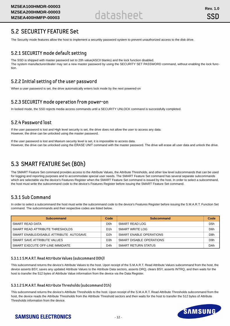
5.3.1 Sub CommandIn order to select a subcommand the host must write the subcommand code to the device's Features Register before issuing the S.M.A.R.T. Function Set command. The subcommands and their respective codes are listed below.
5.3.1.1 S.M.A.R.T. Read Attribute Values (subcommand D0h)l
This subcommand returns the device's Attribute Values to the host. Upon receipt of the S.M.A.R.T. Read Attribute Values subcommand from the host, the device asserts BSY, saves any updated Attribute Values to the Attribute Data sectors, asserts DRQ, clears BSY, asserts INTRQ, and then waits for the host to transfer the 512 bytes of Attribute Value information from the device via the Data Register.
5.3.1.2 S.M.A.R.T. Read Attribute Thresholds (subcommand D1h)
This subcommand returns the device's Attribute Thresholds to the host. Upon receipt of the S.M.A.R.T. Read Attribute Thresholds subcommand from the host, the device reads the Attribute Thresholds from the Attribute Threshold sectors and then waits for the host to transfer the 512 bytes of Attribute Thresholds information from the device.
Subcommand Code Subcommand Code
SMART READ DATA D0h SMART READ LOG D5h
SMART READ ATTRIBUTE THRESHOLDS D1h SMART WRITE LOG D6h
SMART ENABLE/DISABLE ATTRIBUTE AUTOSAVE D2h SMART ENABLE OPERATIONS D8h
SMART SAVE ATTRIBUTE VALUES D3h SMART DISABLE OPERATIONS D9h
SMART EXECUTE OFF-LINE IMMIDIATE D4h SMART RETURN STATUS DAh
- 13 -
MZ5EA400HMFP-00003 SSD Rev. 1.0
MZ5EA200HMDR-00003 datasheetMZ5EA100HMDR-00003
5.3.1.3 S.M.A.R.T. Enable/Disable Attribute Autosave (subcommand D2h)
This subcommand enables and disables the attribute auto save feature of the device. The S.M.A.R.T. Enable/Disable Attribute Autosave subcommand allows the device to automatically save its updated Attribute Values to the Attribute Data Sector at the timing of the first transition to Active idle mode and after 15 minutes after the last saving of Attribute Values. This subcommand causes the auto save feature to be disabled. The state of the Attribute Autosave feature—either enabled or disabled—will be preserved by the device across the power cycle. A value of 00h—written by the host into the device's Sector Count Register before issuing the S.M.A.R.T. Enable/Disable Attribute Autosave subcom-mand—will cause this feature to be disabled. Disabling this feature does not preclude the device from saving Attribute Values to the Attribute Data sectors during some other normal operation such as during a power-up or a power-down.A value of F1h—written by the host into the device's Sector Count Register before issuing the S.M.A.R.T. Enable/Disable Attribute Autosave subcom-mand—will cause this feature to be enabled. Any other nonzero value written by the host into this register before issuing the S.M.A.R.T. Enable/Disable Attribute Autosave subcommand will not change the current Autosave status. The device will respond with the error code specified in Table 7-9: “S.M.A.R.T. Error Codes” on page 30.The S.M.A.R.T. Disable Operations subcommand disables the auto save feature along with the device's S.M.A.R.T. operations.Upon the receipt of the subcommand from the host, the device asserts BSY, enables or disables the Autosave feature, clears BSY, and asserts INTRQ.
5.3.1.4 S.M.A.R.T. Save Attribute Values (subcommand D3h)This subcommand causes the device to immediately save any updated Attribute Values to the device's Attribute Data sector regardless of the state of the Attribute Autosave feature. Upon receipt of the S.M.A.R.T. Save Attribute Values subcommand from the host, the device asserts BSY, writes any updated Attribute Values to the Attribute Data sector, clears BSY, and asserts INTRQ.
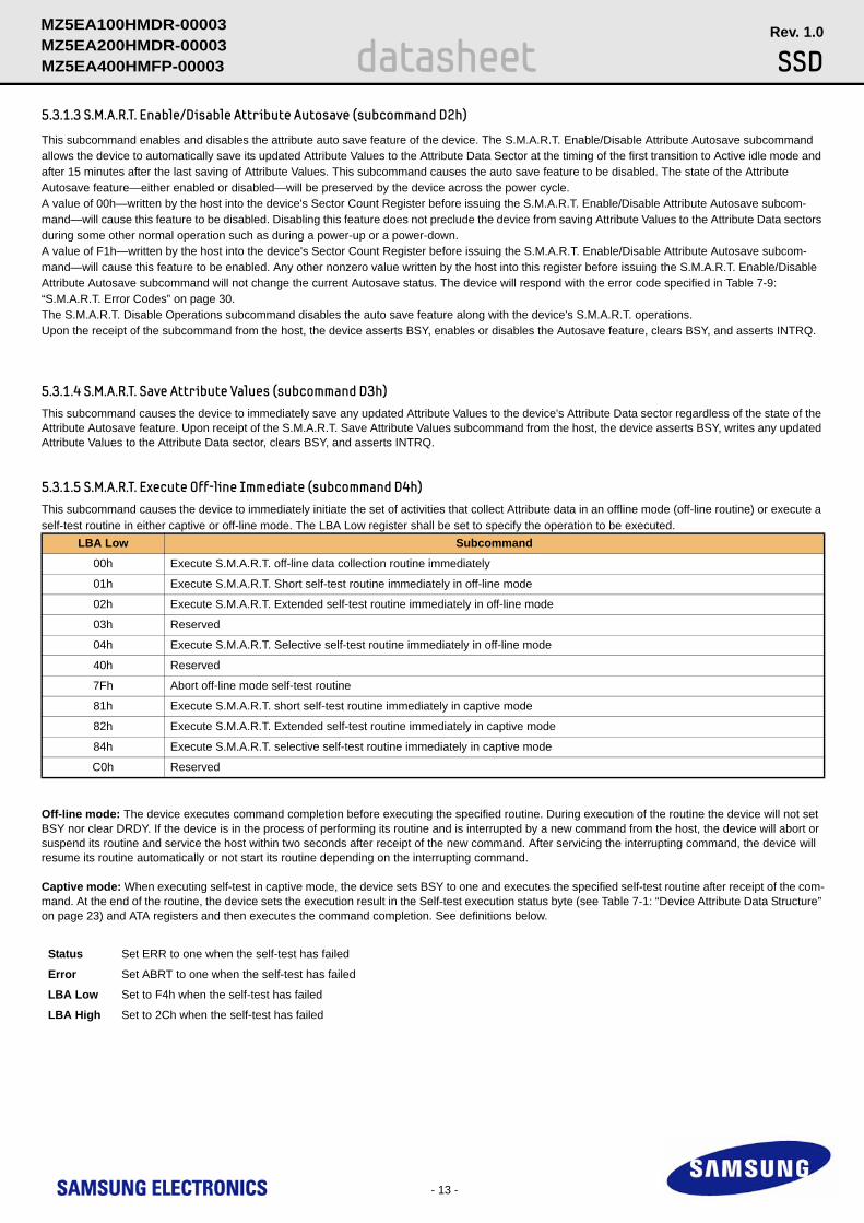
5.3.1.5 S.M.A.R.T. Execute Off-line Immediate (subcommand D4h)This subcommand causes the device to immediately initiate the set of activities that collect Attribute data in an offline mode (off-line routine) or execute a self-test routine in either captive or off-line mode. The LBA Low register shall be set to specify the operation to be executed.
Off-line mode: The device executes command completion before executing the specified routine. During execution of the routine the device will not set BSY nor clear DRDY. If the device is in the process of performing its routine and is interrupted by a new command from the host, the device will abort or suspend its routine and service the host within two seconds after receipt of the new command. After servicing the interrupting command, the device will resume its routine automatically or not start its routine depending on the interrupting command.
Captive mode: When executing self-test in captive mode, the device sets BSY to one and executes the specified self-test routine after receipt of the com-mand. At the end of the routine, the device sets the execution result in the Self-test execution status byte (see Table 7-1: “Device Attribute Data Structure” on page 23) and ATA registers and then executes the command completion. See definitions below.
LBA Low Subcommand
00h Execute S.M.A.R.T. off-line data collection routine immediately
01h Execute S.M.A.R.T. Short self-test routine immediately in off-line mode
02h Execute S.M.A.R.T. Extended self-test routine immediately in off-line mode
03h Reserved
04h Execute S.M.A.R.T. Selective self-test routine immediately in off-line mode
40h Reserved
7Fh Abort off-line mode self-test routine
81h Execute S.M.A.R.T. short self-test routine immediately in captive mode
82h Execute S.M.A.R.T. Extended self-test routine immediately in captive mode
84h Execute S.M.A.R.T. selective self-test routine immediately in captive mode
C0h Reserved
Status Set ERR to one when the self-test has failed
Error Set ABRT to one when the self-test has failed
LBA Low Set to F4h when the self-test has failed
LBA High Set to 2Ch when the self-test has failed
- 14 -
MZ5EA400HMFP-00003 SSD Rev. 1.0
MZ5EA200HMDR-00003 datasheetMZ5EA100HMDR-00003
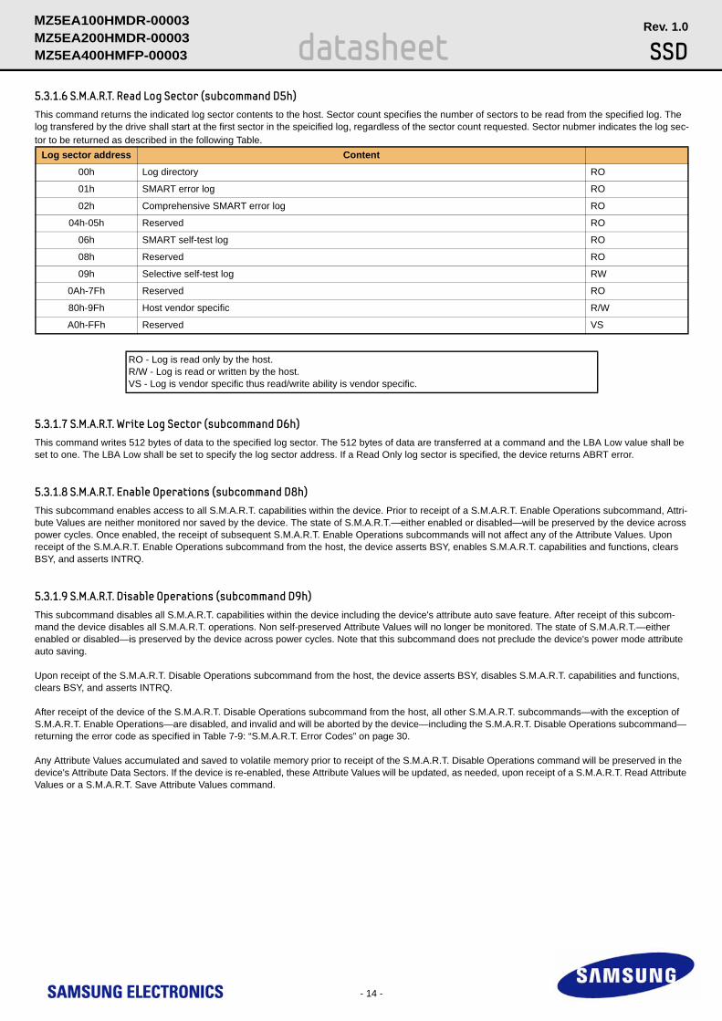
5.3.1.6 S.M.A.R.T. Read Log Sector (subcommand D5h)This command returns the indicated log sector contents to the host. Sector count specifies the number of sectors to be read from the specified log. The log transfered by the drive shall start at the first sector in the speicified log, regardless of the sector count requested. Sector nubmer indicates the log sec-tor to be returned as described in the following Table.
5.3.1.7 S.M.A.R.T. Write Log Sector (subcommand D6h)This command writes 512 bytes of data to the specified log sector. The 512 bytes of data are transferred at a command and the LBA Low value shall be set to one. The LBA Low shall be set to specify the log sector address. If a Read Only log sector is specified, the device returns ABRT error.
5.3.1.8 S.M.A.R.T. Enable Operations (subcommand D8h)This subcommand enables access to all S.M.A.R.T. capabilities within the device. Prior to receipt of a S.M.A.R.T. Enable Operations subcommand, Attri-bute Values are neither monitored nor saved by the device. The state of S.M.A.R.T.—either enabled or disabled—will be preserved by the device across power cycles. Once enabled, the receipt of subsequent S.M.A.R.T. Enable Operations subcommands will not affect any of the Attribute Values. Upon receipt of the S.M.A.R.T. Enable Operations subcommand from the host, the device asserts BSY, enables S.M.A.R.T. capabilities and functions, clears BSY, and asserts INTRQ.
5.3.1.9 S.M.A.R.T. Disable Operations (subcommand D9h)This subcommand disables all S.M.A.R.T. capabilities within the device including the device's attribute auto save feature. After receipt of this subcom-mand the device disables all S.M.A.R.T. operations. Non self-preserved Attribute Values will no longer be monitored. The state of S.M.A.R.T.—either enabled or disabled—is preserved by the device across power cycles. Note that this subcommand does not preclude the device's power mode attribute auto saving.
Upon receipt of the S.M.A.R.T. Disable Operations subcommand from the host, the device asserts BSY, disables S.M.A.R.T. capabilities and functions, clears BSY, and asserts INTRQ.
After receipt of the device of the S.M.A.R.T. Disable Operations subcommand from the host, all other S.M.A.R.T. subcommands—with the exception of S.M.A.R.T. Enable Operations—are disabled, and invalid and will be aborted by the device—including the S.M.A.R.T. Disable Operations subcommand— returning the error code as specified in Table 7-9: “S.M.A.R.T. Error Codes” on page 30.
Any Attribute Values accumulated and saved to volatile memory prior to receipt of the S.M.A.R.T. Disable Operations command will be preserved in the device's Attribute Data Sectors. If the device is re-enabled, these Attribute Values will be updated, as needed, upon receipt of a S.M.A.R.T. Read Attribute Values or a S.M.A.R.T. Save Attribute Values command.
Log sector address Content
00h Log directory RO
01h SMART error log RO
02h Comprehensive SMART error log RO
04h-05h Reserved RO
06h SMART self-test log RO
08h Reserved RO
09h Selective self-test log RW
0Ah-7Fh Reserved RO
80h-9Fh Host vendor specific R/W
A0h-FFh Reserved VS
RO - Log is read only by the host.R/W - Log is read or written by the host.VS - Log is vendor specific thus read/write ability is vendor specific.
- 15 -
MZ5EA400HMFP-00003 SSD Rev. 1.0
MZ5EA200HMDR-00003 datasheetMZ5EA100HMDR-00003
5.3.1.10 S.M.A.R.T. Return Status (subcommand DAh)This subcommand is used to communicate the reliability status of the device to the host's request. Upon receipt of the S.M.A.R.T. Return Status subcom-mand the device asserts BSY, saves any updated Attribute Values to the reserved sector, and compares the updated Attribute Values to the Attribute Thresholds.
If the device does not detect a Threshold Exceeded Condition, or detects a Threshold Exceeded Condition but involving attributes are advisory, the device loads 4Fh into the LBA Mid register, C2h into the LBA High register, clears BSY, and asserts INTRQ.
If the device detects a Threshold Exceeded Condition for prefailure attributes, the device loads F4h into the LBA Mid register, 2Ch into the LBA High reg-ister, clears BSY, and asserts INTRQ. Advisory attributes never result in a negative reliability condition.
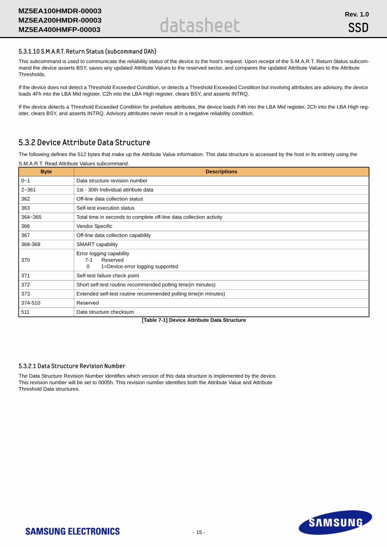
5.3.2 Device Attribute Data StructureThe following defines the 512 bytes that make up the Attribute Value information. This data structure is accessed by the host in its entirety using the
S.M.A.R.T. Read Attribute Values subcommand.
[Table 7-1] Device Attribute Data Structure
5.3.2.1 Data Structure Revision NumberThe Data Structure Revision Number identifies which version of this data structure is implemented by the device.This revision number will be set to 0005h. This revision number identifies both the Attribute Value and AttributeThreshold Data structures.
Byte Descriptions
0~1 Data structure revision number
2~361 1st - 30th Individual attribute data
362 Off-line data collection status
363 Self-test execution status
364~365 Total time in seconds to complete off-line data collection activity
366 Vendor Specific
367 Off-line data collection capability
368-369 SMART capability
370Error logging capability 7-1 Reserved 0 1=Device error logging supported
371 Self-test failure check point
372 Short self-test routine recommended polling time(in minutes)
373 Extended self-test routine recommended polling time(in minutes)
374-510 Reserved
511 Data structure checksum
- 16 -
MZ5EA400HMFP-00003 SSD Rev. 1.0
MZ5EA200HMDR-00003 datasheetMZ5EA100HMDR-00003
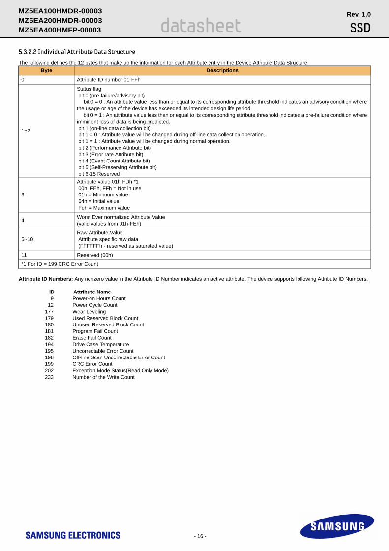
5.3.2.2 Individual Attribute Data Structure
The following defines the 12 bytes that make up the information for each Attribute entry in the Device Attribute Data Structure.
Attribute ID Numbers: Any nonzero value in the Attribute ID Number indicates an active attribute. The device supports following Attribute ID Numbers.
ID Attribute Name 9 Power-on Hours Count 12 Power Cycle Count 177 Wear Leveling 179 Used Reserved Block Count 180 Unused Reserved Block Count 181 Program Fail Count 182 Erase Fail Count 194 Drive Case Temperature 195 Uncorrectable Error Count 198 Off-line Scan Uncorrectable Error Count 199 CRC Error Count 202 Exception Mode Status(Read Only Mode) 233 Number of the Write Count
Byte Descriptions
0 Attribute ID number 01-FFh
1~2
Status flag bit 0 (pre-failure/advisory bit) bit 0 = 0 : An attribute value less than or equal to its corresponding attribute threshold indicates an advisory condition where the usage or age of the device has exceeded its intended design life period. bit 0 = 1 : An attribute value less than or equal to its corresponding attribute threshold indicates a pre-failure condition where imminent loss of data is being predicted. bit 1 (on-line data collection bit) bit 1 = 0 : Attribute value will be changed during off-line data collection operation. bit 1 = 1 : Attribute value will be changed during normal operation. bit 2 (Performance Attribute bit) bit 3 (Error rate Attribute bit) bit 4 (Event Count Attribute bit) bit 5 (Self-Preserving Attribute bit) bit 6-15 Reserved
3
Attribute value 01h-FDh *1 00h, FEh, FFh = Not in use 01h = Minimum value 64h = Initial value Fdh = Maximum value
4 Worst Ever normalized Attribute Value(valid values from 01h-FEh)
5~10Raw Attribute Value Attribute specific raw data (FFFFFFh - reserved as saturated value)
11 Reserved (00h)
*1 For ID = 199 CRC Error Count
- 17 -
MZ5EA400HMFP-00003 SSD Rev. 1.0
MZ5EA200HMDR-00003 datasheetMZ5EA100HMDR-00003
5.3.2.3 Off-Line Data Collection StatusThe value of this byte defines the current status of the off-line activities of the device. Bit 7 indicates an Automatic Off-line Data Collection Status.Bit 7 Automatic Off-line Data Collection Status0 Automatic Off-line Data Collection is disabled.1 Automatic Off-line Data Collection is enabled.
Bits 0–6 represent a hexadecimal status value reported by the device.Value Definition 0 Off-line data collection never started. 2 All segments completed without errors. In this case the current segment pointer is equal to the total segments required. 3 Off-line activity in progress. 4 Off-line data collection is suspended by the interrupting command. 5 Off-line data collecting is aborted by the interrupting command. 6 Off-line data collection is aborted with a fatal error.
5.3.2.4 Self-test execution statusBit Definition0-3 Percent Self-test remaining. An approximation of the percentage of the self-test routine remaining until completion given in ten percent increments. Valid values are 0 through 9.4-7 Current Self-test execution status. 0 The self-test routine completed without error or has never been run. 1 The self-test routine was aborted by the host. 2 The self-test routine was interrupted by the host with a hard or soft reset. 3 The device was unable to complete the self-test routine due to a fatal error or unknown test error. 4 The self-test routine was completed with an unknown element failure. 5 The self-test routine was completed with an electrical element failure. 6 The self-test routine was completed with a servo element failure. 7 The self-test routine was completed with a read element failure. 15 The self-test routine is in progress.
5.3.2.5 Total time in seconds to complete off-line data collection activityThis field tells the host how many seconds the device requires to complete the off-line data collection activity.
5.3.2.6 Current segment pointerThis byte is a counter indicating the next segment to execute as an off-line data collection activity. Because the number of segments is 1, 01h is always returned in this field.
5.3.2.7 Off-line data collection capabilityBit Definition0 Execute Off-line Immediate implemented bit 0 S.M.A.R.T. Execute Off-line Immediate subcommand is not implemented 1 S.M.A.R.T. Execute Off-line Immediate subcommand is implemented1 Enable/disable Automatic Off-line implemented bit 0 S.M.A.R.T. Enable/disable Automatic Off-line subcommand is not implemented 1 S.M.A.R.T. Enable/disable Automatic Off-line subcommand is implemented2 Abort/restart off-line by host bit 0 The device will suspend off-line data collection activity after an interrupting command and resume it after a vendor specific event 1 The device will abort off-line data collection activity upon receipt of a new command Bit Definition3 Off-line Read Scanning implemented bit 0 The device does not support Off-line Read Scanning 1 The device supports Off-line Read Scanning4 Self-test implemented bit 0 Self-test routing is not implemented 1 Self-test routine is implemented5 Reserved (0)6 Selective self-test routine is not implemented 0 Selective self-test routine is not implemented 1 Selective self-test routine is implemented7 Reserved (0)
- 18 -
MZ5EA400HMFP-00003 SSD Rev. 1.0
MZ5EA200HMDR-00003 datasheetMZ5EA100HMDR-00003
5.3.2.8 S.M.A.R.T. CapabilityThis word of bit flags describes the S.M.A.R.T. capabilities of the device. The device will return 03h indicating that the device will save its Attribute Values prior to going into a power saving mode and supports the S.M.A.R.T. ENABLE/DISABLE ATTRIBUTE AUTOSAVE command.Bit Definition0 Pre-power mode attribute saving capability. If bit = 1, the device will save its Attribute Values prior to going into a power saving mode (Standby or Sleep mode).1 Attribute auto save capability. If bit = 1, the device supports the S.M.A.R.T. ENABLE/ DISABLE ATTRIBUTE AUTOSAVE command.2-15 Reserved (0)
5.3.2.9 Error logging capabilityBit Definition7-1 Reserved (0)0 The Error Logging support bit. If bit = 1, the device supports the Error Logging
5.3.2.10 Self-test failure check pointThis byte indicates the section of self-test where the device detected a failure.100
5.3.2.11 Self-test completion timeThese bytes are the minimum time in minutes to complete the self-test.
5.3.2.12 Data Structure ChecksumThe Data Structure Checksum is the 2's complement of the result of a simple 8-bit addition of the first 511 bytes in the data structure.
5.3.3 Device Attribute Thresholds data structureThe following defines the 512 bytes that make up the Attribute Threshold information. This data structure is accessed by the host in its entirety using the S.M.A.R.T. Read Attribute Thresholds. All multibyte fields shown in these data structures follow the ATA/ATAPI-6 specification for byte ordering, that is, that the least significant byte occupies the lowest numbered byte address location in the field. The sequence of active Attribute Thresholds will appear in the same order as their corresponding Attribute Values.
[Table 7-2] Device Attribute Thresholds Data Structure
5.3.3.1 Data Structure Revision NumberThis value is the same as the value used in the Device Attributes Values Data Structure.
Byte Descriptions
0~1 Data structure revision number
2~361 1st - 30th Individual attribute data
362 ~ 379 Reserved
380 ~ 510 Vendor specific
511 Data structure checksum
- 19 -
MZ5EA400HMFP-00003 SSD Rev. 1.0
MZ5EA200HMDR-00003 datasheetMZ5EA100HMDR-00003
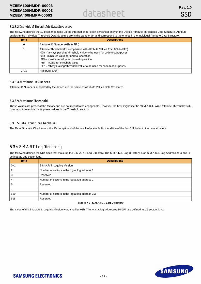
5.3.3.2 Individual Thresholds Data StructureThe following defines the 12 bytes that make up the information for each Threshold entry in the Device Attribute Thresholds Data Structure. Attribute entries in the Individual Threshold Data Structure are in the same order and correspond to the entries in the Individual Attribute Data Structure.
5.3.3.3 Attribute ID NumbersAttribute ID Numbers supported by the device are the same as Attribute Values Data Structures.
5.3.3.4 Attribute ThresholdThese values are preset at the factory and are not meant to be changeable. However, the host might use the "S.M.A.R.T. Write Attribute Threshold" sub-command to override these preset values in the Threshold sectors.
5.3.3.5 Data Structure ChecksumThe Data Structure Checksum is the 2's compliment of the result of a simple 8-bit addition of the first 511 bytes in the data structure.
5.3.4 S.M.A.R.T. Log DirectoryThe following defines the 512 bytes that make up the S.M.A.R.T. Log Directory. The S.M.A.R.T. Log Directory is on S.M.A.R.T. Log Address zero and is defined as one sector long.
[Table 7-3] S.M.A.R.T. Log Directory
The value of the S.M.A.R.T. Logging Version word shall be 01h. The logs at log addresses 80-9Fh are defined as 16 sectors long.
Byte Descriptions
0 Attribute ID Number (01h to FFh)
1 Attribute Threshold (for comparison with Attribute Values from 00h to FFh) 00h - "always passing" threshold value to be used for code test purposes 01h - minimum value for normal operation FDh - maximum value for normal operation FEh - invalid for threshold value FFh - "always failing" threshold value to be used for code test purposes
2~11 Reserved (00h)
Byte Descriptions
0~1 S.M.A.R.T. Logging Version
2 Number of sectors in the log at log address 1
3 Reserved
4 Number of sectors in the log at log address 2
5 Reserved
...
510 Number of sectors in the log at log address 255
511 Reserved
- 20 -
MZ5EA400HMFP-00003 SSD Rev. 1.0
MZ5EA200HMDR-00003 datasheetMZ5EA100HMDR-00003
5.3.5 S.M.A.R.T. error log sectorThe following defines the 512 bytes that make up the S.M.A.R.T. error log sector. All multibyte fields shown in these data structures follow the ATA/ATAPI-6 specifications for byte ordering.
[Table 7-4] S.M.A.R.T. error log sector
5.3.5.1 S.M.A.R.T. error log versionThis value is set to 01h.
5.3.5.2 Error log pointerThis points to the most recent error log data structure. Only values 1 through 5 are valid.
5.3.5.3 Device error countThis field contains the total number of errors. The value will not roll over.
5.3.5.4 Error log data structure
The data format of each error log structure is shown below.
[Table 7-5] Error log data structure
Byte Descriptions
0 S.M.A.R.T. error log version
1 Error log pointer
2-91 1st error log data structure
92-181 2nd error log data structure
182-271 3rd error log data structure
272-361 4th error log data structure
362-451 5th error log data structure
452-453 Device error count
454-510 Reserved
511 Data structure checksum
Byte Descriptions
n ~ n+11 1st command data structure
n+12 ~ n+23 2nd command data structure
n+24 ~ n+35 3rd command data structure
n+36 ~ n+47 4th command data structure
n+48 ~ n+59 5th command data structure
n+60 ~ n+89 Error data structure
- 21 -
MZ5EA400HMFP-00003 SSD Rev. 1.0
MZ5EA200HMDR-00003 datasheetMZ5EA100HMDR-00003
5.3.5.5 Command data structure
Data format of each command data structure is shown below.
[Table 7-6] Command data structure
Timestamp shall be the time since power-on in milliseconds when command acceptance occurred. This timestamp may wrap around.
5.3.5.6 Error data structure
Data format of error data structure is shown below.
[Table 7-7] Error data structure
Extended error information will be vendor specific.
State field contains a value indicating the device state when command was issued to the device.
The value of x is vendor specific and may be different for each state.
Byte Descriptions
n Content of the Device Control register when the Command register was written
n+1 Content of the Features Control register when the Command register was written
n+2 Content of the Sector Count Control register when the Command register was written
n+3 Content of the LBA Low register when the Command register was written
n+4 Content of the LBA Mid register when the Command register was written
n+5 Content of the LBA High register when the Command register was written
n+6 Content of the Device/Head register when the Command register was written
n+7 Content written to the Command register
n+8 Timestamp
n+9 Timestamp
n+10 Timestamp
n+11 Timestamp
Byte Descriptions
n Reserved
n+1 Content written to the Error register after command completion occurred.
n+2 Content written to the Sector Count register after command completion occurred.
n+3 Content written to the LBA Low register after command completion occurred.
n+4 Content written to the LBA Mid register after command completion occurred.
n+5 Content written to the LBA High register after command completion occurred.
n+6 Content written to the Device/Head register after command completion occurred.
n+7 Content written to the Status register after command completion occurred.
n+8 - n+26 Extended error information
n+27 State
n+28 Life Timestamp (least significant byte)
n+29 Life Timestamp (most significant byte)
Value State
x0h Unknown
x1h Sleep
x2h Standby
x3h Active/Idle with BSY cleared to zero
x4h Executing SMART off-line or self-test
x5h-xAh Reserved
xBh-xFh Vendor unique
- 22 -
MZ5EA400HMFP-00003 SSD Rev. 1.0
MZ5EA200HMDR-00003 datasheetMZ5EA100HMDR-00003
5.3.6 Self-test log structure
The following defines the 512 bytes that make up the Self-test log sector.
[Table 7-8] Self-test log data structure
Note: N is 0 through 20The data structure contains the descriptor of the Self-test that the device has performed. Each descriptor is 24 bytes long and the self-test data structure is capable to contain up to 21 descriptors. After 21 descriptors has been recorded, the oldest descriptor will be overwritten with the new descriptor. The self-test log pointer points to the most recent descriptor. When there is no descriptor, the value is 0. When there are descriptor(s), the value is 1 through 21.
5.3.7 Selective self-test log data structureThe Selective self-test log is a log that may be both written and read by the host. This log allows the host to select the parameters for the self-test and to monitor the progress of the self-test. The following table defines the contents of the Selective self-test log which is 512 bytes long. All multi-byte fields
shown in these data structures follow the specifications for byte ordering.
Byte Byte
0~1 Data structure revision
n*24+2 Self-test number
n*24+3 Self-test execution status
n*24+4~n*24+5 Life timestamp
n*24+6 Self-test failure check point
n*24+7~n*24+10 LBA of first failure
n*24+11~n*24+25 Vendor specific
... ...
506~507 Vendor specific
508 Self-test log pointer
509~510 Reserved
511 Data structure checksum
Byte Description Read/Write
0-1 Data structure revision R/W
2-9 Starting LBA for test span 1 R/W
10-17 Ending LBA for test span 1 R/W
18-25 Starting LBA for test span 2 R/W
26-33 Ending LBA for test span 2 R/W
34-41 Starting LBA for test span 3 R/W
42-49 Ending LBA for test span 3 R/W
50-57 Starting LBA for test span 4 R/W
58-65 Ending LBA for test span 4+ R/W
66-73 Starting LBA for test span 5 R/W
74-81 Ending LBA for test span 5 R/W
82-337 Reserved Reserved
338-491 Vendor specific Vendor specific
492-499 Current LBA under test Read
500-501 Current span under test Read
502-503 Feature flags R/W
504-507 Vendor Specific Vendor specific
508-509 Selective self test pending time R/W
510 Reserved Reserved
511 Data structure checksum R/W
- 23 -
MZ5EA400HMFP-00003 SSD Rev. 1.0
MZ5EA200HMDR-00003 datasheetMZ5EA100HMDR-00003
5.3.8 Error reportingThe following table shows the values returned in the Status and Error Registers when specific error conditions are encountered by a device.
[Table 7-9] SMART Error Codes
6.0 SPOR Specification (Sudden Power Off and Recovery)
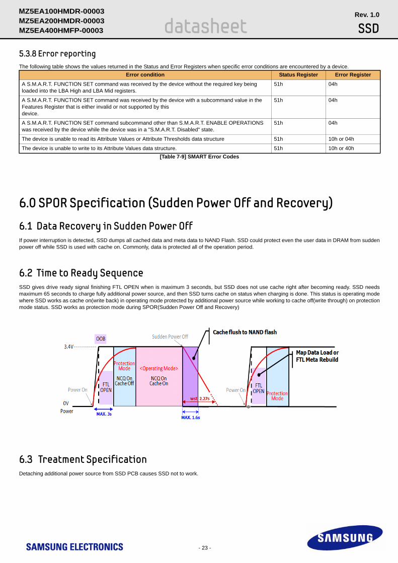
6.1 Data Recovery in Sudden Power OffIf power interruption is detected, SSD dumps all cached data and meta data to NAND Flash. SSD could protect even the user data in DRAM from sudden power off while SSD is used with cache on. Commonly, data is protected all of the operation period.
6.2 Time to Ready SequenceSSD gives drive ready signal finishing FTL OPEN when is maximum 3 seconds, but SSD does not use cache right after becoming ready. SSD needs maximum 65 seconds to charge fully additional power source, and then SSD turns cache on status when charging is done. This status is operating mode where SSD works as cache on(write back) in operating mode protected by additional power source while working to cache off(write through) on protection mode status. SSD works as protection mode during SPOR(Sudden Power Off and Recovery)
6.3 Treatment SpecificationDetaching additional power source from SSD PCB causes SSD not to work.
Error condition Status Register Error Register
A S.M.A.R.T. FUNCTION SET command was received by the device without the required key being loaded into the LBA High and LBA Mid registers.
51h 04h
A S.M.A.R.T. FUNCTION SET command was received by the device with a subcommand value in the Features Register that is either invalid or not supported by thisdevice.
51h 04h
A S.M.A.R.T. FUNCTION SET command subcommand other than S.M.A.R.T. ENABLE OPERATIONS was received by the device while the device was in a "S.M.A.R.T. Disabled" state.
51h 04h
The device is unable to read its Attribute Values or Attribute Thresholds data structure 51h 10h or 04h
The device is unable to write to its Attribute Values data structure. 51h 10h or 40h
- 24 -
MZ5EA400HMFP-00003 SSD Rev. 1.0
MZ5EA200HMDR-00003 datasheetMZ5EA100HMDR-00003
7.0 SATAII Optional Feature
7.1 Power Segment Pin P11Pin P11 of the power segment of the device connector may be used by the device to provide the host with an activity indication and it may be used by the host to indicate whether staggered spinup should be used. To accomplish both of these goals, pin P11 acts as an input from the host to the device prior to PHYRDY for staggered spin-up control and then acts as an output from the device to the host after PHYRDY for activity indication. The activity indication provided by pin P11 is primarily for use in backplane applications.A host may only support one pin P11 feature, either receiving activity indication or staggered spin-up disable control. If a host supports receiving activity indication via pin P11, then the host shall not use pin P11 to disable staggered spin-up. If a host does not support receiving activity indication via pin P11, then the host may use pin P11 to disable staggered spin-up.
7.2 Activity LED indicationThe signal provides for activity indication. This is a low-voltage and low-current driver intended for efficient integration into present and future IC manufac-turing processes. The signal is NOT suitable for directly driving an LED and must first be buffered using a circuit external to the drive before driving and LED. The LED indication signal is working on 200msec periods on FORMAT and Write same command. (100ms at high state and then 100msec at low state) On the other case of commands, the signal is workinig on 100ms periods.
7.3 Asynchronous Signal Recovery Phys may support asynchronous signal recovery for those applications where the usage model of device insertion into a receptacle does not apply. When signal is lost, both the host and the device may attempt to recover the signal. A host or device shall determine loss of signal as represented by a transition from PHYRDY to PHYRDYn, which is associated with entry into states LSI: NoCommErr or LS2:NoComm within the Link layer. Note that negation of PHYRDY does not always constitute a loss of signal. Recovery of the signal is associated with exit from state LS2:NoComm. If the device attempts to recover the signal before the host by issuing a COMINIT, the device shall return its signature following completion of the OOB sequence which included COMINIT. If a host supports asynchronous signal recovery, when the host receives an unsolicited COMINIT, the host shall issue a COMRESET to the device. When a COMRESET is sent to the device in response to an unsolicited COMINIT, the host shall set the Status register to 7Fh and shall set all other Shadow Command Block Registers to FFh. When the COMINIT is received in response to the COMRESET which is associated with entry into state HP2B:HR_AwaitNoCOMINIT, the Shadow Status register value shall be updated to either FFh or 80h to reflect that a device is attached.
- 25 -
MZ5EA400HMFP-00003 SSD Rev. 1.0
MZ5EA200HMDR-00003 datasheetMZ5EA100HMDR-00003
8.0 OOB signaling and Phy Power State
8.1 OOB signaling
8.1.1 OOB signal spacingThere shall be three Out Of Band (OOB) signals used/detected by the Phy: COMRESET,COMINIT, and COMWAKE. Each burst is followed by idle peri-ods (at common-mode levels), having durations as depicted in following Figure and Table. The COMWAKE OOB signaling is used to bring the Phy out
of a power-down state (Partial or Slumber)
8.2 Phy Power State
8.2.1 COMRESET sequence state diagram
8.2.2 Interface Power States
8.2.2.1 PHYRDY
The Phy logic and main PLL are both on and active. The interface issynchronized and capable of receiving and sending data.
8.2.2.2 Partial
The Phy logic is powered, but is in a reduced power state. Both signal lines on the interface are at a neutral logic state (common mode voltage). The exit latency from this state shall be no longer than 10 us.
8.2.2.3 Slumber
The Phy logic is powered but is in a reduced power state. The exit latency from this state shall be no longer than 10 ms.
8.2.3 Partial/Slumber to PHYRDY
8.2.3.1 Host Initiated
The host may initiate a wakeup from the Partial or Slumber states by entering the power-on sequence at the “Host COMWAKE” point in the state machine. Calibration and speed negotiation is bypassed since it has already been performed at power-on and system performance depends on quick resume latency. The device, therefore, shall transmit ALIGNP primitives at the speed determined at power-on.
8.2.3.2 Device Initiated
The device may initiate a wakeup from the Partial or Slumber states by entering the power-on sequence at the “Device COMWAKE” point in the state machine. Calibration and speed negotiation is bypassed since it has already been performed at power-on and system performance depends on quick resume latency. The device, therefore, shall transmit ALIGNP primitives at the speed determined at power-on.
8.2.4 PHYRDY to Partial/Slumber
8.2.4.1 Host Initiated for Partial
8.2.4.2 Device Initiated for Partial*For Slumber, the same sequence applies except PMREQ_PP is replaced with PMREQ_SP and Partial is replaced with Slumber.
Time Value
T1 106.7 ns
T2 320 ns
- 26 -
MZ5EA400HMFP-00003 SSD Rev. 1.0
MZ5EA200HMDR-00003 datasheetMZ5EA100HMDR-00003
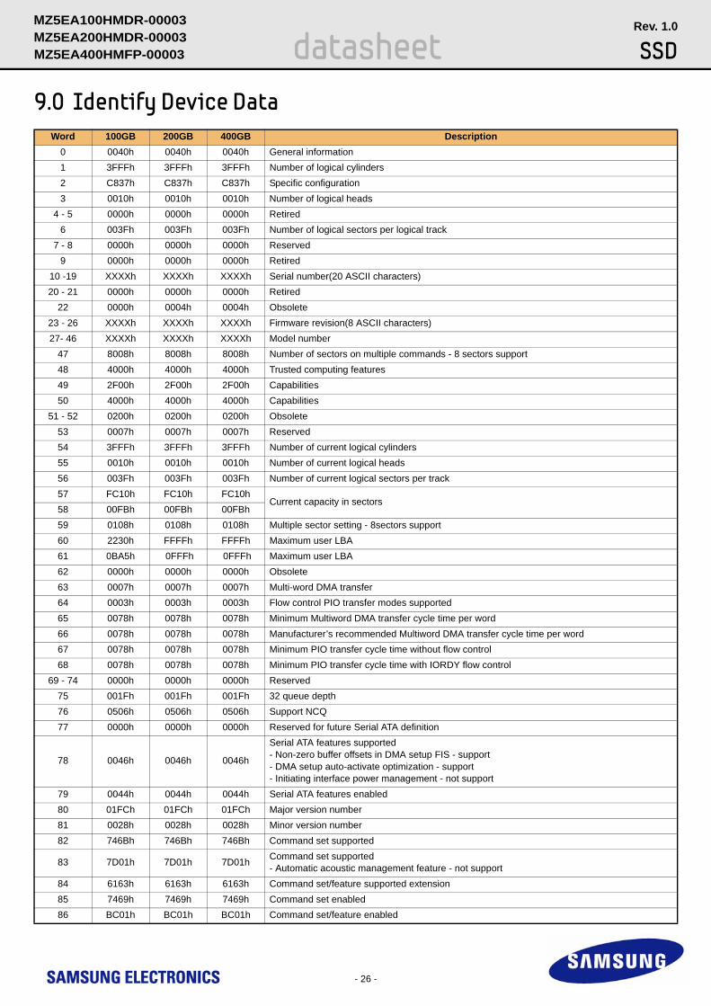
9.0 Identify Device DataWord 100GB 200GB 400GB Description
0 0040h 0040h 0040h General information1 3FFFh 3FFFh 3FFFh Number of logical cylinders2 C837h C837h C837h Specific configuration3 0010h 0010h 0010h Number of logical heads
4 - 5 0000h 0000h 0000h Retired6 003Fh 003Fh 003Fh Number of logical sectors per logical track
7 - 8 0000h 0000h 0000h Reserved 9 0000h 0000h 0000h Retired
10 -19 XXXXh XXXXh XXXXh Serial number(20 ASCII characters)20 - 21 0000h 0000h 0000h Retired
22 0000h 0004h 0004h Obsolete23 - 26 XXXXh XXXXh XXXXh Firmware revision(8 ASCII characters)27- 46 XXXXh XXXXh XXXXh Model number
47 8008h 8008h 8008h Number of sectors on multiple commands - 8 sectors support48 4000h 4000h 4000h Trusted computing features 49 2F00h 2F00h 2F00h Capabilities50 4000h 4000h 4000h Capabilities
51 - 52 0200h 0200h 0200h Obsolete53 0007h 0007h 0007h Reserved54 3FFFh 3FFFh 3FFFh Number of current logical cylinders55 0010h 0010h 0010h Number of current logical heads56 003Fh 003Fh 003Fh Number of current logical sectors per track57 FC10h FC10h FC10h
Current capacity in sectors58 00FBh 00FBh 00FBh59 0108h 0108h 0108h Multiple sector setting - 8sectors support60 2230h FFFFh FFFFh Maximum user LBA61 0BA5h 0FFFh 0FFFh Maximum user LBA62 0000h 0000h 0000h Obsolete63 0007h 0007h 0007h Multi-word DMA transfer64 0003h 0003h 0003h Flow control PIO transfer modes supported65 0078h 0078h 0078h Minimum Multiword DMA transfer cycle time per word66 0078h 0078h 0078h Manufacturer’s recommended Multiword DMA transfer cycle time per word67 0078h 0078h 0078h Minimum PIO transfer cycle time without flow control68 0078h 0078h 0078h Minimum PIO transfer cycle time with IORDY flow control
69 - 74 0000h 0000h 0000h Reserved75 001Fh 001Fh 001Fh 32 queue depth76 0506h 0506h 0506h Support NCQ77 0000h 0000h 0000h Reserved for future Serial ATA definition
78 0046h 0046h 0046h
Serial ATA features supported- Non-zero buffer offsets in DMA setup FIS - support- DMA setup auto-activate optimization - support- Initiating interface power management - not support
79 0044h 0044h 0044h Serial ATA features enabled80 01FCh 01FCh 01FCh Major version number81 0028h 0028h 0028h Minor version number82 746Bh 746Bh 746Bh Command set supported
83 7D01h 7D01h 7D01h Command set supported- Automatic acoustic management feature - not support
84 6163h 6163h 6163h Command set/feature supported extension85 7469h 7469h 7469h Command set enabled86 BC01h BC01h BC01h Command set/feature enabled
- 27 -
MZ5EA400HMFP-00003 SSD Rev. 1.0
MZ5EA200HMDR-00003 datasheetMZ5EA100HMDR-00003
Word 100GB 200GB 400GB Description87 6163h 6163h 6163h Command set/feature default88 407Fh 407Fh 407Fh Ultra DMA mode 6 is selected89 0001h 0001h 0001h Time required for security erase unit completion90 0001h 0001h 0001h Time required for Enhanced security erase complete91 0000h 0000h 0000h Current advanced power management value92 FFFEh FFFEh FFFEh Master Password Revision Code93 0000h 0000h 0000h Hardware reset result94 0000h 0000h 0000h Current automatic acoustic management value - not support
95-99 0000h 0000h 0000h Reserved100 2230h F1B0h 90B0h Maximum user LBA101 0BA5h 1749h 2E93h Maximum user LBA
102-103 0000h 0000h 0000h Maximum user LBA104-105 0000h 0000h 0000h Compliant with IDEMA Standard
106 4000h 4000h 4000h Compliant with IDEMA Standard107 0000h 0000h 0000h Compliant with IDEMA Standard
108-111 XXXXh XXXXh XXXXh Reserved for World Wide Name112-115 0000h 0000h 0000h Reserved116-118 0000h 0000h 0000h Compliant with IDEMA Standard
119-120 401Eh 401Eh 401EhCompliant with IDEMA Standard- Write, read, verify feature set - support- Read log dma ext, write log dma ext - support
121-126 0000h 0000h 0000h Compliant with IDEMA Standard127 0000h 0000h 0000h Removable Media Status Notification feature set supported128 0021h 0021h 0021h Security status
129-159 0000h 0000h 0000h Reserved160 0000h 0000h 0000h CFA power mode1
161-167 0000h 0000h 0000h Reserved168 0003h 0003h 0003h Reserved
169-175 0000h 0000h 0000h Reserved176-205 0000h 0000h 0000h Current media serial number
206 003Fh 003Fh 003Fh SCT command transport support207 - 208 0000h 0000h 0000h Reserved
209 4000h 4000h 4000h Init value210 - 216 0000h 0000h 0000h Reserved
217 0001h 0001h 0001h Non-rotating Media Device218-221 0000h 0000h 0000h Reserved
222 101Fh 101Fh 101Fh Support SATA Rev 2.6, SATA Rev 2.5, SATA II: Extensions,SATA 1.0a, ATA8223-234 0000h 0000h 0000h Reserved
235 0080h 0080h 0080h Maximum number of 512 byte data blocks per DOWNLOAD MICROCODE cmd for mode 03h236-254 0000h 0000h 0000h Reserved
255 5CA5h 53A5h 53A5h Integrity word
- 28 -
MZ5EA400HMFP-00003 SSD Rev. 1.0
MZ5EA200HMDR-00003 datasheetMZ5EA100HMDR-00003
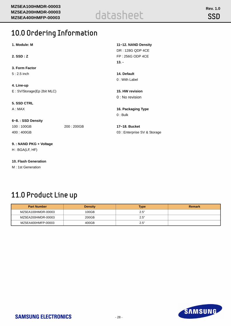
10.0 Ordering Information
11.0 Product Line up
1. Module: M 11~12. NAND DensityDR : 128G QDP 4CE
2. SSD : Z FP : 256G ODP 4CE
13. - 3. Form Factor5 : 2.5 inch 14. Default
0 : With Label
4. Line-upE : SV/Storage(Ep 2bit MLC) 15. HW revision
0 : No revision5. SSD CTRLA : MAX 16. Packaging Type
0 : Bulk
6~8. : SSD Density100 : 100GB 200 : 200GB 17~18. Bucket400 : 400GB 03 : Enterprise SV & Storage
9. : NAND PKG + VoltageH : BGA(LF, HF)
10. Flash GenerationM : 1st Generation
Part Number Density Type Remark
MZ5EA100HMDR-00003 100GB 2.5"
MZ5EA200HMDR-00003 200GB 2.5"
MZ5EA400HMFP-00003 400GB 2.5"