Embed Size (px)
Citation preview
Small Size Defected Ground Structure (DGS) Coupled Resonator Band Pass Filters with Capacitor Loaded Slot Using FDTD Method
ADEL ABD ELRAHMAN, ADEL ZEIN ELDEIN, AHMED ABD ELMONEM, and HESHAM
FATHI Faculty of Engineering, High Institute of Energy
The higher institute for Engineering and Technology, Faculty of Engineering South Valley University-Qena, South Valley University, Aswan, El-Minia, El-Minia
[email protected], [email protected] [email protected], [email protected]
Abstract: - This paper presents a design of a small size second and third order band pass coupled resonator filters by using finite difference time domain method (FDTD). Two of the proposed filters consist of compact folded DGS resonators, the other consists of compact rectangular DGS resonators and a lumped capacitor is combined within the slot of each filter. The insertion of lumped capacitor within resonators increases the effective capacitance, and reduces the resonant frequency, so the dimensions of the filter will reduce and the performance of the filter will be improved by enhancing the energy stored in the resonator. The resonance bandwidth is decreased leading to increasing the resonator quality factor. A second order band pass filter with centre frequency of 2.4 GHz has been designed, fabricated and measured. The filter has a wide stop band with a rejection higher than 20 dB up to more than 10 GHz. Insertion loss of less than 0.7 dB is achieved within the pass band. Another second order band pass filter with centre frequency of 3.1 GHz has been designed, fabricated, and measured. The filter has a wide stop band with a rejection higher than 20 dB up to more than 10 GHz. Insertion loss of less than 0.8 dB has been achieved within the pass band. It is found that, the experimental results agree well with the EM-simulation and FDTD simulation results. Finally, a third order band pass filter with center frequency of 2.4GHZ with single transmission zero at 2.61 GHz is designed and simulated. The filter has pass band from 2.3 to 2.52 GHz and wide stop band with rejection higher than 20 dB up to more than 8GHZ, and insertion loss lower than 1 dB is achieved within pass band.
.Key-Words: - Band Pass Filter, Coupled resonator filter, Defected ground structure, Lumped capacitor, FDTD
1 Introduction Modern microwave communication systems require miniaturized high-performance band pass filters with high selectivity and wide stop band response. These filters can be designed and fabricated on various materials. Planar filters are particularly attractive because of their smaller size, easier manufacture, and lower fabrication cost [1]. With the development of wireless communication, the more crowded the spectrum is, the more stringent specifications for designing filters are. These specifications have become harder to be met by conventional Butterworth and Chebyshev filters. Now it is cross coupled filters with finite transmission zeros that the best choices are, which are carried out by the general Chebyshev function. Compared with conventional filters, it can not only meet specifications, but also reduce the number of resonating elements and this, in turn, reduces the insertion loss, size, and manufacturing cost of the design. But it is more complicated to synthesis and
design than conventional filters. Researchers have proposed various configurations for reducing the size of filters and improving filter performance. Several compact and high performance components have been reported by using DGS for the microstrip line [2-8]. DGS has been attractive to obtain the function of unwanted frequency rejection and circuit size reduction. Variable capacitors are used in filter application for minimizing the size of resonators and tuning their resonant frequencies [9-10]. The time-dependent Maxwell's equations in partial differential form are discretized using central difference approximations to the space and time partial derivatives. The resulting finite-difference equations are solved in software in a leapfrog manner, the electric field vector components, in a volume of space, are solved at a given instant in time; then the magnetic field vector components in the same spatial volume are solved at the next instant in time; and the process is repeated over and over again until the desired transient or steady-state
WSEAS TRANSACTIONS on COMMUNICATIONSAdel Abd Elrahman, Adel Zein Eldein, Ahmed Abd Elmonem, Hesham Fathi
ISSN: 1109-2742 88 Issue 3, Volume 10, March 2011
electromagnetic field behavior is fully evolved. The finite difference time domain method (FDTD) was initially used to solve the EM scattering problem by Taflove [11] in 1975 which is the first break through in FDTD history. In this paper we propose an improvement on the performance of band pass coupled resonator filter by combining lumped capacitor in the slot of resonator at place, which has maximum electric field. Also, in this paper a study of the effect of capacitance on the resonant frequency is investigated and good agreement is achieved between the simulation results and the results from FDTD method program. Finally compact band pass second and third order is designed using EM simulator program. It is found that the simulation results obtained from the 3-D EM simulator program, are in good agreement with FDTD code and measurement results.
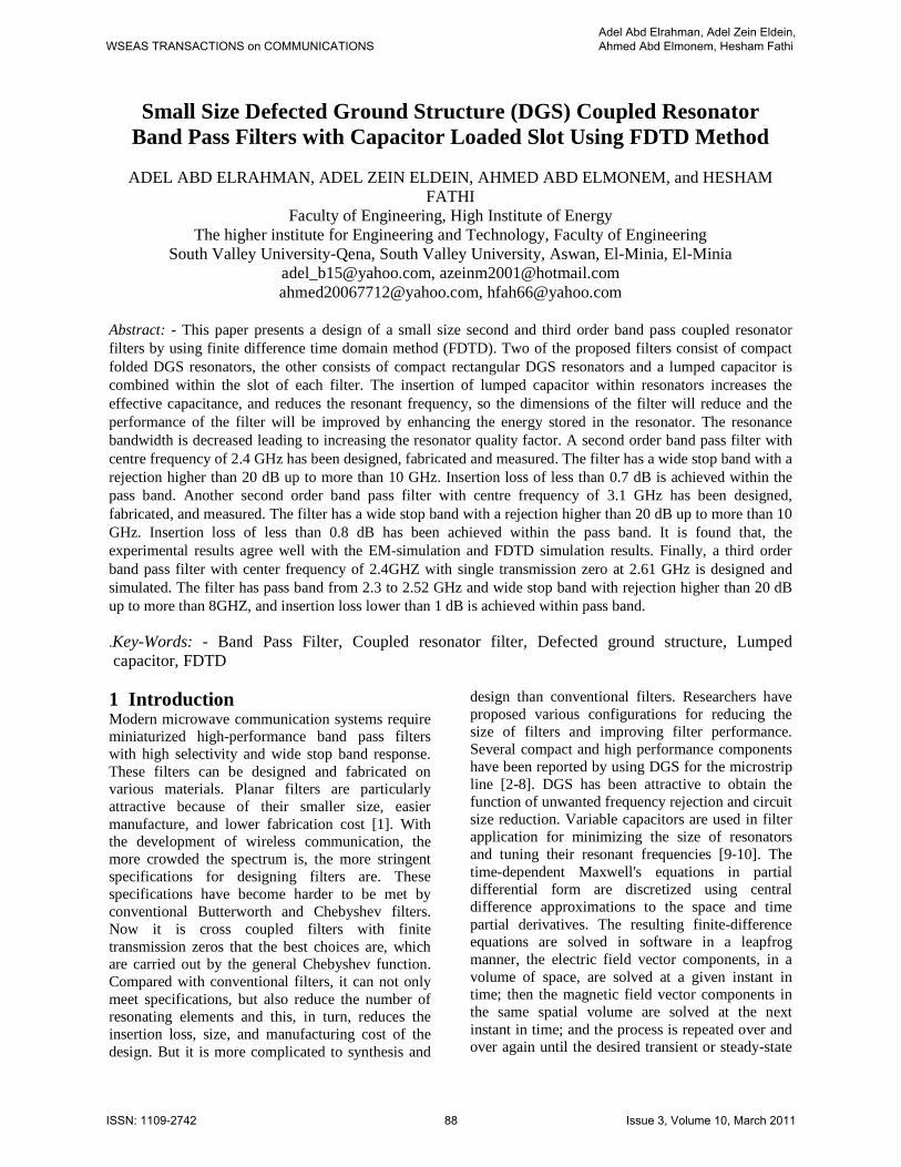
2 The Finite Difference Time Domain Method 2.1The Finite Difference Time Domain Method Basic Equations The FDTD algorithm divides the problem geometry into a spatial grid where electric and magnetic field components are placed at certain discrete positions in space, and it solves Maxwell’s equations in time at discrete time instances. This can be implemented by first approximating the time and space derivatives appearing in Maxwell’s equations by finite differences and next by constructing a set of equations that calculate the values of fields at a future time instant from the values of fields at a past time instant. The starting point for the construction of an FDTD algorithm is Maxwell’s time-domain equations. The differential time-domain Maxwell’s equations needed to specify the field behaviour over time are [12]:
Substituting for the time and space derivatives at time step n and at space lattice point (i,j,k), we have initially
In a similar manner, we can derive finite-difference expressions based on Yee's algorithm for the Hy and Hz field components given by Maxwell's equations [12]. We can derive finite-difference expressions based on Yee's algorithm for the Ex, Ey, and Ez field components given by Maxwell's equations where
2/1+nEσ represents the loss term on the right-hand side of each equation, which is estimated using approximation procedure analogous to that of equation (4) that results in a set of three equations having a form similar to that of the H equations above, and Ex can be written as [12]:
2.2 Numerical Stability The numerical algorithms for Maxwell's curl equations defined by the finite difference systems require that the time increment t∆ have a specific bound relative to the lattice space increments x∆ ,
y∆ , and z∆ . This bound is necessary to avoid numerical instability, an undesirable possibility with explicit differential equation solvers that can cause the computed results to spuriously increase without limit as time marching continues. Electromagnetic wave propagation in free space cannot go faster than the speed of the light. The choice of cell size is critical in applying FDTD. It must be small enough to permit accurate results at the highest frequency of interest. Cell size is directly affected by the
HEt
H
µρ
µ−×∇−=
∂∂ 1
(1)
EHt
E
εσ
ε−×∇−=
∂∂ 1
(2)
−∆
−
−∆
−
⋅=∆
−
−+
−+−+
n
kjixkji
n
kjiz
n
kjiz
n
kjiy
n
kjiy
kji
n
kjix
n
kjix
Hy
EE
z
EE
t
HH
,,,,,2/1,,2/1,
2/1,,2/1,,
,,
2/1
,,
2/1
,, 1
ρµ
(3)
2
2/1
,,
2/1
,,
,,
−+ −=
n
kjix
n
kjixn
kjix
HHH
(4)
∆
−
−∆
−
⋅
∆+
∆
+
∆+
∆−
=−+
−+
−+
y
EE
z
EE
t
t
Ht
t
Hn
kjiz
n
kjiz
n
kjiy
n
kjiy
kji
kji
kjin
kjix
kji
kji
kji
kji
n
kjix
,2/1,,2/1,
2/1,,2/1,,
,,
,,
,,2/1
,,
,,
,,
,,
,,
2/1
,,
21
21
21
µρµ
µρµ
ρ
(5)
∆
−
−∆
−
⋅
∆+
∆
+
∆+
∆−
=+
−
+
+
+
−
+
+
+
z
HH
y
HH
t
t
Et
t
En
kjiy
n
kjiy
n
kjiz
n
kjiz
kji
kji
kjin
kjix
kji
kji
kji
kji
n
kjix 2/1
2/1,,
2/1
2/1,,
2/1
,2/1,
2/1
,2/1,
,,
,,
,,
,,
,,
,,
,,
,,
1
,,
21
21
21
εσε
εσ
εσ
(6)
WSEAS TRANSACTIONS on COMMUNICATIONSAdel Abd Elrahman, Adel Zein Eldein, Ahmed Abd Elmonem, Hesham Fathi
ISSN: 1109-2742 89 Issue 3, Volume 10, March 2011
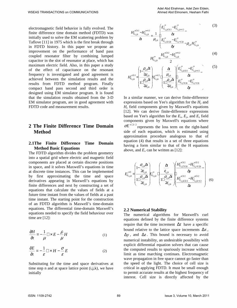
materials present. The greater the permittivity the shorter the wavelength at a given frequency and smaller the cell size required. The fundamental constraint is the cell size must be much less than the smallest wavelength for which accurate results are desired. The side of each cell size should be 1/10λ or less at the highest frequency (shorter wave length) of interest. The Courant condition in 3-dimensions is [13]:
Where; v is the speed of the light, experience has indicated that for actual computations the t∆ value given by above equations will provide accurate results.
2.3 Gaussian Waveform A Gaussian waveform is the best choice for a source waveform, since it can be constructed to contain all frequencies up to a highest frequency that is tied to a cell size by a factor. This factor, which is the proportion of the highest frequency wavelength to the unit cell size, is referred as number of cells per wavelength. A Gaussian waveform can be written as a function of time as [14]:
where τ is a parameter that determines the width of the Gaussian pulse and t0 is the amount of time shift. We can find t0 and τ as [14]:
2.4 Modelling of Lumped Capacitor Consider the insertion of a numerical lumped capacitor into the FDTD grid. Assuming a z-directed lumped element located in free space at
kjizE,,
, the voltage-current characteristic that
describes the capacitor's behaviour in a semi-implicit manner is [15]:
Fig.1 Flow chart of FDTD program
222
111
1
zyxv
t
∆+
∆+
∆
≤∆ (7)
( )( )
2
20
τtt
etg−
−=
(8)
max
3.2
f⋅=
πτ (9)
ττ 5.4200 ≅=t (10)
Start
Set problem space and define parameters
Set initial values for electric and
magnetic fields
Compute field coefficients
Define Gaussian pulse as a
source
Calculation magnetic fields
Hn+1/2
Update magnetic field
components
Calculation electric fields En+1
Update electric field
components
Apply boundary conditions
No
Computing voltage and current
around feed point
Increment time step, n= n+1
Yes
Last iterations
Output data
Current and voltage Stop
WSEAS TRANSACTIONS on COMMUNICATIONSAdel Abd Elrahman, Adel Zein Eldein, Ahmed Abd Elmonem, Hesham Fathi
ISSN: 1109-2742 90 Issue 3, Volume 10, March 2011
Where, С is the value of the capacitance. The corresponding time-stepping relation is [15]:
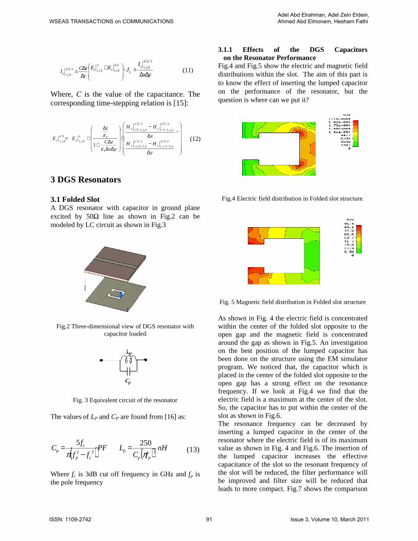
3 DGS Resonators 3.1 Folded Slot A DGS resonator with capacitor in ground plane excited by 50Ω line as shown in Fig.2 can be modeled by LC circuit as shown in Fig.3
Fig.2 Three-dimensional view of DGS resonator with capacitor loaded
Fig. 3 Equivalent circuit of the resonator The values of LP and CP are found from [16] as:
( ) ( ) nHfC
LPFff
fC
pp
p
cp
cp 222
2505
ππ=
−= (13)
Where fc is 3dB cut off frequency in GHz and fp is the pole frequency
3.1.1 Effects of the DGS Capacitors on the Resonator Performance Fig.4 and Fig.5 show the electric and magnetic field distributions within the slot. The aim of this part is to know the effect of inserting the lumped capacitor on the performance of the resonator, but the question is where can we put it?
Fig.4 Electric field distribution in Folded slot structure.
Fig. 5 Magnetic field distribution in Folded slot structure
As shown in Fig. 4 the electric field is concentrated within the center of the folded slot opposite to the open gap and the magnetic field is concentrated around the gap as shown in Fig.5. An investigation on the best position of the lumped capacitor has been done on the structure using the EM simulator program. We noticed that, the capacitor which is placed in the center of the folded slot opposite to the open gap has a strong effect on the resonance frequency. If we look at Fig.4 we find that the electric field is a maximum at the center of the slot. So, the capacitor has to put within the center of the slot as shown in Fig.6. The resonance frequency can be decreased by inserting a lumped capacitor in the center of the resonator where the electric field is of its maximum value as shown in Fig. 4 and Fig.6. The insertion of the lumped capacitor increases the effective capacitance of the slot so the resonant frequency of the slot will be reduced, the filter performance will be improved and filter size will be reduced that leads to more compact. Fig.7 shows the comparison
+∆∆=
++
1
,,,,2/1
,,
n
kjiz
n
kjizn
kjiz
EE
t
zCI
,yx
IJ
n
kjiz
L ∆∆=
+ 2/1
,, (11)
∆
−
−∆
−
⋅
∆∆∆+
∆
+=+
−
+
+
+
−
+
+
+
y
HH
x
HH
yx
zC
t
EEn
kjix
n
kjix
n
kjiy
n
kjiy
n
kjiz
n
kjiz 2/1
,2/1,
2/1
,2/1,
2/1
,,2/1
2/1
,,2/1
0
0
,,
1
,,
1ε
ε
(12)
WSEAS TRANSACTIONS on COMMUNICATIONSAdel Abd Elrahman, Adel Zein Eldein, Ahmed Abd Elmonem, Hesham Fathi
ISSN: 1109-2742 91 Issue 3, Volume 10, March 2011
between the design of folded resonator with FDTD method and EM simulator program, where a good agreement is achieved between their results.
Fig.6 DGS resonator with lumped capacitor
Fig.7 EM and FDTD Simulation results of folded slot resonator with and without lumped capacitor
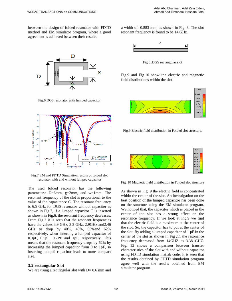
The used folded resonator has the following parameters: D=6mm, g=2mm, and w=1mm. The resonant frequency of the slot is proportional to the value of the capacitance C. The resonant frequency is 6.5 GHz for DGS resonator without capacitor as shown in Fig.7, if a lumped capacitor C is inserted as shown in Fig.6, the resonant frequency decreases. From Fig.7 it is seen that the resonant frequencies have the values 3.9 GHz, 3.3 GHz, 2.9GHz and2.46 GHz or drop by 40%, 49%, 55%and 62% respectively, when inserting a lumped capacitor of 0.3pF, 0.5pF, 0.7PF and 1pF, respectively. This means that the resonant frequency drops by 62% by increasing the lumped capacitor from 0 to 1pF, so inserting lumped capacitor leads to more compact size. 3.2 rectangular Slot We are using a rectangular slot with D= 8.6 mm and
a width of 0.883 mm, as shown in Fig. 8. The slot resonant frequency is found to be 14 GHz.
Fig.8 .DGS rectangular slot
Fig.9 and Fig.10 show the electric and magnetic field distributions within the slot.
Fig.9 Electric field distribution in Folded slot structure.
Fig. 10 Magnetic field distribution in Folded slot structure
As shown in Fig. 9 the electric field is concentrated within the center of the slot. An investigation on the best position of the lumped capacitor has been done on the structure using the EM simulator program. We noticed that, the capacitor which is placed in the center of the slot has a strong effect on the resonance frequency. If we look at Fig.9 we find that the electric field is a maximum at the center of the slot. So, the capacitor has to put at the center of the slot. By adding a lumped capacitor of 1 pF in the center of the slot as shown in Fig .11 the resonance frequency decreased from 14GHZ to 3.38 GHZ. Fig. 12 shows a comparison between transfer characteristics of the slot with and without capacitor using FDTD simulation matlab code. It is seen that the results obtained by FDTD simulation program agree well with the results obtained from EM simulator program.
D
WSEAS TRANSACTIONS on COMMUNICATIONSAdel Abd Elrahman, Adel Zein Eldein, Ahmed Abd Elmonem, Hesham Fathi
ISSN: 1109-2742 92 Issue 3, Volume 10, March 2011
Fig.11 DGS rectangular slot with lumped capacitor
Fig. 12 Comparison of insertion Loss S21of short slot with and without capacitor
3.2.1 Effect of Capacitor on Compactness To verify the compactness of the structure, we have simulated the transfer characteristics for the proposed slot with lumped capacitor and a long rectangular slot as shown in Fig .13, with D=36mm and has the same width of 0.883mm of that gave the same resonant frequency. The lumped capacitor basically controls the resonator capacitance. The proposed structure gave size reduction, where the length of the slot is reduced by more than 75% as shown from Fig. 8.and Fig.13.
Fig.13 DGS Long rectangular slot.
Fig. 14 compares transfer characteristics of the proposed compact resonating slot and rectangular long slot. It seen that the proposed structure exhibit free wide pass band compared to the long slot.
Fig.14 Comparison of insertion Loss S21 of long slot without capacitor and short slot with capacitor
4 Design of Second Order coupled Resonator Filters 4.1 Second Order Coupled Resonator Filter Depend on Folded Slot 4.1.1 Coupling Coefficient Fig.15 illustrates coupling structure and the curve of the coupling coefficient that results from the orientation of pair of identical DGS resonators which are separated by spacing S. The coupling coefficient shown in Fig.15 is extracted using EM simulator by coupling the structure very weakly to a 50 Ω microstrip feed. The coupling coefficients can be also extracted from the separation frequencies [17].
Fig.15 Coupling coefficients for DGS resonators (Mixed coupling).
D
D
S
WSEAS TRANSACTIONS on COMMUNICATIONSAdel Abd Elrahman, Adel Zein Eldein, Ahmed Abd Elmonem, Hesham Fathi
ISSN: 1109-2742 93 Issue 3, Volume 10, March 2011
4.1.2 External Quality Factor As shown in Fig.16, the external coupling is realized by a 50 Ω microstrip line, on the other side of the substrate extended by a stub d. The value of the external quality factor is extracted from the full-wave EM simulator. The resonant frequency of these resonators affected slightly when the feed line is slightly extended by a stub with length d. The 50 Ω microstrip line is perpendicular (with stub) to the resonator.
Fig.16 External coupling (quality factor)
4.1.3 Filter synthesis, Realization and Design Realization coupling matrix which conforms for chosen topology is extracted when first we define the filter specification using an optimization-based scheme [18, 19]. The coupling coefficient and quality factor curves are then used to realize the obtained coupling coefficients [17]. A second order filter has the following parameters: bandwidth BW = 270 MHz, return loss RL =18 dB, and centre frequency f0=2.4 GHz. The obtained coupling matrix from the optimization scheme is [18]
=
049.1
49.10M
(14)
and the external quality factors are q1 = q2 = 1.31. To realize the normalized coupling matrix and quality factors, we use the required fractional bandwidth
of
BWFBW =
(15)
the actual (denormalized) coupling matrix becomes
6.1121
0167.0
167.00
==
=
m (16)
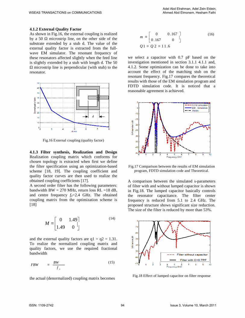
we select a capacitor with 0.7 pF based on the investigation mentioned in section 3.1.1 4.1.1 and, 4.1.2. Some optimization can be done to take into account the effect of the matching stub on the resonant frequency. Fig.17 compares the theoretical results with those of the EM simulation program and FDTD simulation code. It is noticed that a reasonable agreement is achieved.
Fig.17 Comparison between the results of EM simulation program, FDTD simulation code and Theoretical.
A comparison between the simulated s-parameters of filter with and without lumped capacitor is shown in Fig.18. The lumped capacitor basically controls the resonator capacitance. The filter center frequency is reduced from 5.1 to 2.4 GHz. The proposed structure shows significant size reduction. The size of the filter is reduced by more than 53%.
Fig.18 Effect of lumped capacitor on filter response
d
WSEAS TRANSACTIONS on COMMUNICATIONSAdel Abd Elrahman, Adel Zein Eldein, Ahmed Abd Elmonem, Hesham Fathi
ISSN: 1109-2742 94 Issue 3, Volume 10, March 2011
4.1.4 Experimental Results The designed filter has been fabricated on a high frequency printed circuit board RO4003 with a relative dielectric constant of 3.38 and a thickness of 0.813 mm. The 50 Ω microstrip feed line has width of 1.92 mm. Fig. 19 shows the filter that consists of two coupled resonators. Each resonator consists of folded slot loaded by capacitor at its center. A stub is used to match the 50 Ω microstrip line to the resonator by moving the feed line to a distance equals to d. While Fig. 20 shows a photograph of the fabricated compact bandpass coupled resonator filter using the capacitor loaded DGS resonators. The lumped capacitors are soldered at the centre of the slots. Fig. 21 shows an experimentally confirmation for the designed filter. Also, it is seen that a good agreement between EM simulation, FDTD method and measured results has been achieved.
Fig.19a 3-D view of the DGS coupled resonators filter slot
Fig.19b Coupled resonator filter configuration
Fig.20a Photograph of the fabricated filter (top view )
Fig.20b Photograph of the fabricated filter (bottom view )
Fig.21Comparison between EM simulation , measurement and FDTD simulation of a second order filter
4.2 Second Order Coupled Resonator Filter Depend on Rectangular Slot The aim of this part is to design second order coupled resonator filter with center frequency fo=3.1GHZ, band width BW=640MHZ, and return loss RL=18dB using the compact resonating rectangular slot as a building block for a coupled resonator filter. The proposed filter is shown in Fig. 22. It consists of two identical compact coupled resonators. Each resonator consists of a rectangular slot, loaded by lumped capacitor at its center. The feed strip width of 1.9 mm is chosen for a characteristic impedance of 50 Ω. A stub is used to match the 50 Ω microstrip feed line to the resonator.
0.4 mm
2 mm
d
6mm
6mm
1 mm
WSEAS TRANSACTIONS on COMMUNICATIONSAdel Abd Elrahman, Adel Zein Eldein, Ahmed Abd Elmonem, Hesham Fathi
ISSN: 1109-2742 95 Issue 3, Volume 10, March 2011
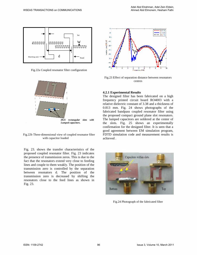
Fig.22a Coupled resonator filter configuration
Fig.22b Three-dimensional view of coupled resonator filter with capacitor loaded
Fig. 23. shows the transfer characteristics of the proposed coupled resonator filter. Fig. 23 indicates the presence of transmission zeros. This is due to the fact that the resonators extend very close to feeding lines and couple to them weakly. The position of the transmission zero is controlled by the separation between resonators d. The position of the transmission zero is decreased by shifting the resonators close to the feed lines as shown in Fig. 23.
Fig.23 Effect of separation distance between resonators centres
4.2.1 Experimental Results The designed filter has been fabricated on a high frequency printed circuit board RO4003 with a relative dielectric constant of 3.38 and a thickness of 0.813 mm. Fig. 24 shows photographs of the fabricated bandpass coupled resonator filter using the proposed compact ground plane slot resonators. The lumped capacitors are soldered at the center of the slots. Fig. 25 shows an experimentally confirmation for the designed filter. It is seen that a good agreement between EM simulation program, FDTD simulation code and measurement results is achieved .
Fig.24 Photograph of the fabricated filter
d Matching stub Feed
lot
W
DGS rectangular slots with Lumped capacitors.
WSEAS TRANSACTIONS on COMMUNICATIONSAdel Abd Elrahman, Adel Zein Eldein, Ahmed Abd Elmonem, Hesham Fathi
ISSN: 1109-2742 96 Issue 3, Volume 10, March 2011
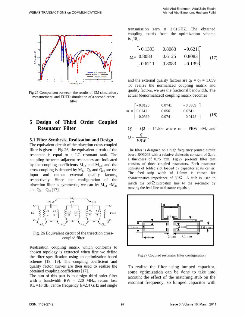
Fig.25 Comparison between the results of EM simulation , measurement and FDTD simulation of a second order
filter 5 Design of Third Order Coupled Resonator Filter 5.1 Filter Synthesis, Realization and Design The equivalent circuit of the trisection cross-coupled filter is given in Fig.26, the equivalent circuit of the resonator is equal to a LC resonant tank. The coupling between adjacent resonators are indicated by the coupling coefficients M12 and M23, and the cross coupling is denoted by M13. Qei and Qeo are the input and output external quality factors, respectively. Since the configuration of the trisection filter is symmetric, we can let M12 =M23 and Qei = Qeo [17].
Fig. 26 Equivalent circuit of the trisection cross-coupled filter
Realization coupling matrix which conforms to chosen topology is extracted when first we define the filter specification using an optimization-based scheme [18, 19]. The coupling coefficient and quality factor curves are then used to realize the obtained coupling coefficients [17]. The aim of this part is to design third order filter with a bandwidth BW = 220 MHz, return loss RL =18 dB, centre frequency f0=2.4 GHz and single
transmission zero at 2.61GHZ. The obtained coupling matrix from the optimization scheme is [18].
M=
0.1393-
0.8083
0.6211-
0.8083
0.6125
0.8083
0.6211-
0.8083
0.1393-
(17)
and the external quality factors are q1 = q2 = 1.059 To realize the normalized coupling matrix and quality factors, we use the fractional bandwidth. The actual (denormalized) coupling matrix becomes
=0.0128-
0.0741
0.0569-
0.0741
0.0561
0.0741
0.0569-
0.0741
0.0128-
m
(18)
Q1 = Q2 = 55.11 where m = FBW ×M, and
Q = FBW
q.
The filter is designed on a high frequency printed circuit board RO3003 with a relative dielectric constant of 3and a thickness of 0.75 mm. Fig.27 presents filter that consists of three coupled resonators. Each resonator consists of folded slot loaded by capacitor at its center. The feed strip width of 1.9mm is chosen for characteristics impedance of 50Ω . A stub is used to
match the 50Ω microstrip line to the resonator by moving the feed line to distance equals d.
Fig.27 Coupled resonator filter configuration
To realize the filter using lumped capacitor, some optimization can be done to take into account the effect of the matching stub on the resonant frequency, so lumped capacitor with
7.1 mm
2 mm
7.1 mm
d 2 mm
0.6 mm 0.8 mm
1.9 mm
WSEAS TRANSACTIONS on COMMUNICATIONSAdel Abd Elrahman, Adel Zein Eldein, Ahmed Abd Elmonem, Hesham Fathi
ISSN: 1109-2742 97 Issue 3, Volume 10, March 2011
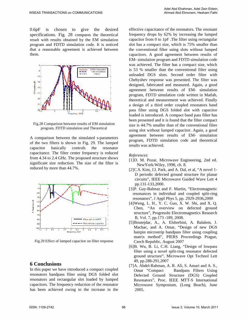
0.6pF is chosen to give the desired specifications. Fig. 28 compares the theoretical result with results obtained by the EM simulation program and FDTD simulation code. It is noticed that a reasonable agreement is achieved between them.
Fig.28 Comparison between results of EM simulation program, FDTD simulation and Theoretical
A comparison between the simulated s-parameters of the two filters is shown in Fig. 29. The lumped capacitor basically controls the resonator capacitance. The filter center frequency is reduced from 4.34 to 2.4 GHz. The proposed structure shows significant size reduction. The size of the filter is reduced by more than 44.7%.
Fig.29 Effect of lumped capacitor on filter response
6 Conclusions In this paper we have introduced a compact coupled resonators bandpass filter using DGS folded slot resonators and rectangular slot loaded by lumped capacitors. The frequency reduction of the resonator has been achieved owing to the increase in the
effective capacitance of the resonators. The resonant frequency drops by 62% by increasing the lumped capacitor from 0 to 1pF .The filter using rectangular slot has a compact size, which is 75% smaller than the conventional filter using slots without lumped capacitors. A good agreement between results of EM- simulation program and FDTD simulation code was achieved. The filter has a compact size, which is 53 % smaller than the conventional filter using unloaded DGS slots. Second order filter with Chebyshev response was presented. The filter was designed, fabricated and measured. Again, a good agreement between results of EM- simulation program, FDTD simulation code written in Matlab, theoretical and measurement was achieved. Finally a design of a third order coupled resonators band pass filter using DGS folded slot with capacitor loaded is introduced. A compact band pass filter has been presented and it is found that the filter compact size is 44.7% smaller than of the conventional filter using slot without lumped capacitor. Again, a good agreement between results of EM- simulation program, FDTD simulation code and theoretical results was achieved. References: [1] D. M. Pozar, Microwave Engineering, 2nd ed. NewYork:Wiley, 1998, ch. 8.
[2] C.S. Kim, J.I. Park, and A. Dal, et al, “A novel 1- D periodic defected ground structure for planar circuits”, IEEE Microwave Guided Wave Lett 4 pp.131-133,2000.
[3] P. Gay-Balmaz and F. Martin, “Electromagnetic resonances in individual and coupled split-ring resonators”, J Appl Phys 5, pp. 2929-2936,2000
[4] Weng, L. H., Y. C. Guo, X. W. Shi, and X. Q. Chen, “An overview on defected ground structure”, ProgressIn Electromagnetics Research B, Vol. 7, pp.173 -189, 2008.
[5] Boutejdar, A., A. Elsherbini, A. Balalem, J. Machac, and A. Omar, “Design of new DGS hairpin microstrip bandpass filter using coupling matrix method”, PIERS Proceedings Prague, Czech Republic, August 2007
[6] B. Wu, B. Li, C.H. Liang, “Design of lowpass filter using a novel split-ring resonator defected ground structure”, Microwave Opt Technol Lett 49, pp.288-291,2007
[7] A. Abdel-Rahman, A. R. Ali, S. Amari and A. S., Omar “Compact Bandpass Filters Using Defected Ground Structure (DGS) Coupled Resonators”, Proc. IEEE MTT-S International Microwave Symposium, (Long Beach), June 2005.
WSEAS TRANSACTIONS on COMMUNICATIONSAdel Abd Elrahman, Adel Zein Eldein, Ahmed Abd Elmonem, Hesham Fathi
ISSN: 1109-2742 98 Issue 3, Volume 10, March 2011
[8] Adel B. Abdel-Rahman, Adel Z. El Dein, Hesham F. A. Hamed, Ahmed A. Ibrahim, “Small Size Third Order Coupled Resonator Band-Pass Filter Using Capacitor Loaded Slots”, IEEE APS, Middle East Conference on Antennas and Propagation (MECAP),Cairo, Egypt, 2010
[9] M. Makimoto, and M Sagawa, ‘‘Varactor tuned bandpass filter using microstrip-line ring resonators,’’ IEEE MTT-S Digst, Int. Microw Sypo ., pp.411-414, June 1986.
[10] X. H. Wang, B. Z. Wang, H. Zhang, and K. J. Chen, ‘‘A tunable bandstop resonator based on a compact slotted ground structure,’’ IEEE Transaction on Microwave Theory and Techniques, Vol. 55, No. 9, pp. 1912-1918.
[11] Taflove A. and Brodwin M. E., “Numerical solution of stead state electromagnetic scattering problems using the time dependent Maxewell’s equations”, IEEE Trans. Microwave Theory Tech. vol.23, no.8 pp. 623- 630, Aug. 1975.
[12] Allen Taflove, “Computational Electrodynamics: The Finite- Difference Time-Domain Method”. Artech House Publishers.1995.
[13] Karls.Kunz,Raymond J.Lubbers “The finite difference time domain method for electromagnetics”,CRC press, 1993
[14] Atef Elsherbeni, Veysel Demir, ”The finite difference time domain method for electromagnetics with mATLAB simulations”, October 2008
[15] Piket May M. J., A. Taflove, and J. Baron, “FD-TD modeling of digital signal propagation in 3-D circuits with passive and active loads”, IEEE Trans. Microwave Theory and Techniques, vol. 42, pp. 1514-1523, 1994.
[16] A. Abdel-Rahman, A. K. Verma, A. Boutejdar and A. S. Omar, “Control of Band Stop Response of Hi- Low Microstrip Low pass Filter Using Slot in Ground Plane”, IEEE Trans. Microwave Theory Tech., vol. 52, No. 3, pp. 1008-1013, Mar. 2004.
[17] Hong, J. S. and M. J. Lancaster, Microstrip Filters for RF/Microwave Applications, Wiley, New York, 2001.
[18] S. Amari, “Synthesis of Cross-Coupled Resonator Filters Using an Analytical Gradiant- Based Optimi-zation Technique”, IEEE Trans. Microwave Theory Tech., vol. 48, No. 9, pp. 1559-1564, Sep. 2000
[19] A. B. Jayyousi and M. J. Lancaster, “A gradient-Based Optimization Technique Employing Determi-nants for the Synthesis of Microwave Coupled Filters”, IEEE, MTT-S, PP. 1369-1372,2004
WSEAS TRANSACTIONS on COMMUNICATIONSAdel Abd Elrahman, Adel Zein Eldein, Ahmed Abd Elmonem, Hesham Fathi
ISSN: 1109-2742 99 Issue 3, Volume 10, March 2011


![DOI: Design of … · 2017-07-18 · and soldering as compared to the proposed UWB BPF. The UWB bandpass filter presented in [4] is based on defected ground structure (DGS) as split](https://img.pdfslide.net/doc/110x75/5eb2c954259f77427962b90d/doi-design-of-2017-07-18-and-soldering-as-compared-to-the-proposed-uwb-bpf-the.jpg)