Embed Size (px)
Citation preview

Smart Device Fabrication Strategies
for Solution Processed Solar Cells
Intelligente Herstellungsstrategien für lösungsprozessierte
Solarzellen
Der Technischen Fakultät
der Friedrich-Alexander- Universität
Erlangen- Nürnberg
zur
Erlangung des Doktorgrades Dr.- Ing.
vorgelegt von
Georgios Spyropoulos
aus Amaroussio, Greece

ii 2016 FAU Erlangen-Nürnberg
Als Dissertation genehmigt
von der Technischen Fakultät
der Friedrich-Alexander-Universität Erlangen-Nürnberg
Tag der mündlichen Prüfung: 13 / 01 / 2017
Vorsitzender des Promotionsorgans: Prof. Dr. –Ing. Reinhard Lerch
1. Gutachter: Prof. Dr. Christoph J. Brabec
2. Gutachter: Prof. Dr. Siegfried Bauer

2016 FAU Erlangen-Nürnberg iii
Dedicated to my parents; Dimitris Spyropoulos and Vassiliki Spyropoulou
my grandparents; Georgios Sypropoulos, Anastasia Spyropoulou and Efrosini Georgara
and a very inspirational person; Babis Nikolaidis

iv 2016 FAU Erlangen-Nürnberg
“People do not decide their futures,
they decide their habits and their habits decide their futures“
− Frederick Matthias Alexander

2016 FAU Erlangen-Nürnberg v
Zusammenfassung Intelligente Herstellungsstrategie für Lösungsprozessierte Solarzellen
Die Dünnschicht-Photovoltaik ist eine Schlüsseltechnologie im Bereich der erneuerbaren
Energien, da sie die Umwandlung von Licht in günstige Energie durch die Anwendung
lösungsprozessierter Drucktechniken wie zum Beispiel Rolle-zu-Rolle Verfahren erlaubt.
Zudem ermöglichen verformbare Substrate ästhetisch ansprechende, mechanisch flexible und
individualisierbare Module. Diese erleitern die elektronischen Anwendungen und die
Einbindung in architektonische Objekte. Der Fokus dieser Dissertation ist die Entwicklung
neuer Materialien und Herstellungsmethoden für lösungsprozessierte Solarzellen, welche
anschließend einfach vom Labormaßstab in den Produktionsmaßstab für Rolle-zu-Rolle
Verfahren übertragen werden können. Bei der Wahl der Materialien und Verfahren wurde
berücksichtigt, dass dabei nicht die Effizienz der Energieumwandlung als auch die Stabilität
und die Flexibilität geopfert wurden. Die physikalischen Eigenschaften von Materialen, die
aus der Lösung prozessiert wurden, wurden untersucht, um stabile, qualitativ hochwertige,
dünne Filme mit einer bestimmten Funktionalität innerhalb der Solarzellenarchitektur zu
erzielen. Dies umfasst Untersuchungen an Loch-/Elektron-Transportschichten, photoaktiven
Schichten und Elektroden. Es wurden gezielt intelligente Fertigungsverfahren entwickelt, um
langsame und kostenintensive Prozesse zu vermeiden. Desweiteren wurde die Möglichkeit
des Hochskalierens von Prototypen, welche die bisherigen wissenschaftlich und experimentell
gesetzten Grenzen überschreiten, anhand der Kombination verschiedener Materialsysteme
und Herstellungsmethoden mit neuartigen Techniken zur Laserstrukturierung demonstriert.
Die bisher beschriebenen Aspekte werden deutlich an Hand meines Kernprojektes ersichtlich,
bei dem zusammen mit Kolleg(inn)en Folgendes gezeigt wurde: i) die Anwendung von Rolle-
zu-Rolle nahen Verfahren für hocheffiziente, flexible, lösungsprozessierte organische
Tandem-Solarzellenmodule; ii) die Gewährleistung von langen Lebensdauern von Solarzelle;
iii) die Entwicklung eines innovativen lösungsprozessierten Herstellungsverfahren für
effiziente organische sowie Perovskite-Solarzellenmodule mittels einer tiefenselektiven
Laserstrukturierung; iv) basierend auf dem zuletzt erwähnten Herstellungsansatz wurde dieser
neuartige Prozess auf Module mit mehrfachen Halbleiter-Halbleiter Übergängen übertragen,
indem zwei individuell getrennt fabrizierte Solarzellen durch Laminieren in Serie geschaltet
wurden. Die sich daraus ergebenden Erkenntnisse sind ausschlaggebende Schritte in Richtung
effizienter, stabiler und flexibler Photovoltaik..

vi 2016 FAU Erlangen-Nürnberg
Acknowledgements
I would like to express my gratitude to my supervisor, Prof. Dr. Christoph Brabec not
only for giving me the opportunity to join a fantastic, multi-cultural group which improved
me as a scientist and human being, but also because he never constricted my scientific
curiosity and creativity.
I am very grateful to Dr. Tayebeh Ameri for her academic support, supervision and her
constant belief on my skills and passion. I would like also to thank Dr. Hans Egelhaaf for our
fruitful discussions and his scientific support. My special thanks go to Dr. Ning Li who
reinforced me with friend support and constructive scientific discussions. Additionally, I
would like to thank Dr. Jens Adams, Dr. Peter Kubis and Yi Hou for their contribution to my
work and their patience when I have been importunate. I could not but thank the people
responsible for the nice environment of my office; Stephan Lagner and Jose Dario Perea.
During my thesis time, I have been very lucky to meet people that made me believe I was
never far from home; Luca Lucera, Derya Baran, Michael Salvador, Nicola Gasparini and
Cesar Omar Ramirez Quiroz. They all contributed to this thesis with both moral and scientific
support. Apart from that, they create for me amazing memories here in Germany and they
have gained specific place in my heart.
Last but not least, I would like to thank my family in Greece for their emotional support
and their philosophy to invest in intellectual property and not in material goods.

2016 FAU Erlangen-Nürnberg vii
List of Abbreviations Ag Silver
AgNW Silver Nanowire
AM1.5G Air Mass 1.5 Global
AZO Aluminum doped Zinc Oxide
Ba(OH)2 Barium Hydroxide
BHJ Bulk-heterojunction
DLIT Dark Lock-In Thermography
Eg Bandgap
EHOMO Energy Level of Highest Occupied Molecular Orbital
EIS Electrochemical Impedance Spectroscopy
ELUMO Energy Level of Lowest Unoccupied Molecular Orbital
ETL Electron Transporting Layer
EQE External Quantum Efficiency
FF Fill Factor
GaAs Gallium Arsenide
GFF Geometric Fill Factor
HOMO Highest Occupied Molecular Orbital
HTL Hole Transporting Layer
I Current
IMI Indium Tin Oxide-Metal-Indium Tin Oxide
IML Intermediate Layer
IMPP Current at Maximum Point
IPA Isopropyl Alcohol
Iph Intensity of spectrum of the light source
IQE Internal Quantum Efficiency
ITO Indium Tin Oxide
JMPP Current Density at Maximum Power Point
Jsc Short Circuit Current Density
J-V Current Density-Voltage
LUMO Lowest Unoccupied Molecular Orbital
MPP Maximum Power Point
MoOx Molybdenum Oxide
NiO Nickel Oxide
OLED Organic Light Emitting Diode
OPV Organic Photovoltaic
OPV12 Polymer Donor received from Polyera
OSC Organic Solar Cell
P3HT Poly(3-hexylthiophene-2,5-diyl)
PBTZT-stat-
BDTT-8 Polymer Donor received from Merck
[60]PCBM [6,6]-phenyl C61 butyric acid methyl ester
[70]PCBM [6,6]-phenyl C71 butyric acid methyl ester
pDPP5T-2 Diketopyrrolopyrrole-quinquethiophene alternating copolymer
PEDOT:PSS Poly(3,4 ethylenedioxythiophene):poly(styrenesulfonate)
PEI Polyethylenimine
Rp Parallel Resistance

viii 2016 FAU Erlangen-Nürnberg
Rs Series Resistance
SEM Scanning Electron Microscopy
T Temperature
TCA Transparent Conductive Adhesive
UV Ultra Violet
VMPP Voltage at Maximum Power Point
ZnO Zinc Oxide
k Boltzmann Constant
h Planck’s constant
ν Frequency
q Elementary Charge
ΔE Energetic Loss
μ Mobility
π – π* pi-pi*
σ – σ* sigma-sigma*

2016 FAU Erlangen-Nürnberg ix
List of Figures Figure 1-1: Average isolation of earth for years 1991-1993. The black disks correspond
to the theoretical area that covered with 8% efficient solar cells would give 18TW yearly,
which corresponds to a value higher than the world’s total primary energy demand.3, 4
........... 1
Figure 1-2: Research cell efficiency records chart presented from National Center for
Photovoltaics(NREL)14
.............................................................................................................. 2
Figure 1-3: a) Roll-to-roll production of OPVs. (source: OPV infinity) b) Modern life
application for flexible OPVs (source: OPV infinity) c) Solar leaf (part of a product from
Belectric OPV GmbH, source: www.solarte.de). d),e) Integration of OPVs in architectural
objects (product from Belectric OPV GmbH appeared in EXPO Milan 2015, source: www.solarte.de). f) Integration of OPVs on a bus stop rooftop in San Francisco (source:
demonstrator from Konarka) ..................................................................................................... 4
Figure 1-4: a) Organo-metal-halide active layer on glass (credit: Boshu Zhang, Wong
Choon Lim Glenn & Mingzhen Liu) b) IMEC presented perovskite photovoltaic modules
with 11% PCE.53
c) Flexible perovskite solar module presented by F.D.Giacomo et al.54 ....... 5
Figure 1-5: a) Types of tandem solar cells separated by the terminal connections. b)AM
1.5 global spectrum and a schematic representation of a multijunction device comprising three
sub-cells with complementary absorption spectra. Note that cell 1, cell 2 and cell 3 correspond
to cells with different Eg. Optimally the light meets the cell with the highest band gap first. .. 6
Figure 1-6: Different geometries for plasmon light trapping in OPVs; a) scattering from
large diameter (>50 nm) metal nanoparticles into high angles inside photoactive layer,
causing increased optical path length. b) Localized surface plasmon resonance induced by
small diameter (5–20 nm) metal particles. c) Excitation of surface plasmon polaritons at the
NPs/photoactive layer interfaces ensures the coupling of incident light to photonic modes
propagating in the semiconductor layer plane. Reproduced with permission.113
..................... 13
Figure 1-7: Illustration of up and down conversion processes. a) Up conversion process.
Two photons with energy 1/2 Eg convert in one photon with energy Eg. The optimal position
of up converting layer is before the photoactive layer (light meets up converter first).b) Down
conversion process. One photon with energy Eg converts in two photons with energy 1/2 Eg.
.................................................................................................................................................. 14
Figure 1-8: Simplistic illustration of split spectrum solar cells. The incident light is split
by spectrally sensitive mirrors and sent to the corresponding solar cell. Cell 1,2 and 3 have
different band gaps and they can be connected in series or in parallel configuration. ............. 15
Figure 1-9: Band diagram of a solar cell with intermediate band. Conduction band (CB),
valence band (VB) and intermediate band (IB) are shown. Intermediate band solar cell can
absorb different photons with different energies (presented here with different colors). ........ 15
Figure 1-10: Schematic illustration of multiple electron-hole pair generation. Blue wave
represents the incident photon, while orange wave represent the heat energy from the relaxing
electron that generate a second exciton. ................................................................................... 16
Figure 1-11: Schematic illustration of a the components of a thermophotovoltaic system.
Narrow bandwidth light is emitted from thermal emitter and control by a spectral control
element. Excess energy is emitted from the cell back to be recycled. ..................................... 17

x 2016 FAU Erlangen-Nürnberg
Figure 1-12: a) ITO replacement market forecast (source: Touch Display Research, ITO replacement: non-ITO Transparent Conductor Technologies and Market Forecast 2015 Report, 2015) b) Cost vs conductivity estimation of ITO-replacement technologies (source: Source: Touch Display Research Inc., ITO-Replacement Report, January 2016) .................. 18
Figure 1-13: Schematic illustration for 0-dimensional and 1-dimensional coating
techniques. Slot die coating and spray coating can produce patterns with shims and shadow
masks correspondingly (details in text). Modified with permission.167
................................... 23
Figure 1-14: Schematic illustrations of 2-dimesional printing techniques. Modified with
permission.167
........................................................................................................................... 25
Figure 1-15: Schematic illustration of the principles behind drop on demand
piezoelectric inkjet printing and continuous inkjet printing. Modified with permission.167
.... 26
Figure 1-16: The three necessary “gears” for any photovoltaic technology. .................. 28
Figure 2-1: a) The formation of σ and π bonding and π, π* orbitals in its simplest form
for a molecule of ehtene. b) The corresponding energy diagram. The illustration shows the
optical excitation from π (HOMO) to π* (LUMO) orbitals. .................................................... 31
Figure 2-2: Bilayer vs bulk heterojunction structures. The exciton separation occurs at
interfaces. Bulk heterojunction is more efficient because of the limited exciton diffusion
length in organic materials. Reproduced with permission.184
.................................................. 32
Figure 2-3: Operating principles of bulk heterojunction solar cell. Left: Simplified
kinetics diagram. Right: Simplified energy diagram.(i) Singlet exciton generation. (ii) Exciton
diffusion. (iii) Exciton dissociation. (iv) Charge separation. (v) Charge transport. (vi) Charge
extraction. Reproduced with permission.183
............................................................................ 33
Figure 2-4: Energy levels present in a donor–acceptor system which are relevant to the
mechanisms of generation, recombination and dissociation of CT complexes. Reproduced
with permission183
.................................................................................................................... 34
Figure 2-5: a) Perovskite crystal structure of the form ABX3. b) The energy diagram of
CH3NH3PbI3 perovskite resulted from the antibonding orbitals of the bonds between Pb (B)
and I (X). The illustration shows the optical excitation highest occupied state to the lowest
unoccupied state. ...................................................................................................................... 36
Figure 2-6: Structural evolution of perovskite solar cells: (a) sensitization concept with
surface adsorption of nanodot perovskite, (b) meso-superstructure concept with non-injecting
scaffold layer, (c) pillared structure with a nano oxide building block, and (d) planar p-i-n
heterojunction concept. Spheres represent TiO2 in (a) and (c) and Al2O3 in (b). Reproduced
with permission.188
................................................................................................................... 38
Figure 2-7: Schematic illustration of energy levels and processes in a perovskite solar
cell employing TiO2 and an HTM. ........................................................................................... 39
Figure 2-8: Normal architecture for single junction (a) and tandem solar cell (c). Inverted
architecture of single junction (b) and tandem solar cells (d). ................................................. 40
Figure 2-9: Transmittance versus sheet resistance for promising solution processed
electrodes.164, 212-214
Transmittance values were obtained at ~550nm. The bulk regime
(described by equation 2.3) is shown with solid line. The percolation regime (described by
equation 2.7) is shown with dashed line.133
............................................................................. 43
Figure 2-10: a) Linear and b) semi-logarithmic presentation of J-V curves und dark and
illuminated conditions. Reproduced with permission.183
......................................................... 43

2016 FAU Erlangen-Nürnberg xi
Figure 2-11: Single diode equivalent circuit model commonly employed in estimating
electrical losses in solar cell. .................................................................................................... 45
Figure 2-12: a) PCE prediction of a bulk heterojunction solar cell with PCBM as
acceptor material. For the calculation Scharber et al. assumed FF of 75%, EQE of 80% and
Voc according to Eq.2.13. b) Simplified energy diagram of a donor acceptor system.
Reproduced with permission.220
............................................................................................... 51
Figure 2-13: Theoretical efficiency of bulk-heterojunction photovoltaic devices with Eg−
qVoc= 0.60 eV (solid line) versus the lowest optical bandgap of the two materials, calculated
using the AM1.5 spectrum, FF = 0.65, and assuming constant EQE = 0.65 between 3.5 eV
and Eg . The dashed lines show the theoretical efficiencies for devices using the larger Eg −
qV oc offsets for (from top to bottom): PF10TBT:[60]PCBM (0.70 eV,circles),
PCPDTBT:[70]PCBM (0.76 eV, down triangles), PBBTDPP2:[70]PCBM (0.80 eV, up
triangles), and P3HT:[60]PCBM (1.09 eV, squares). The closed markers represent the
theoretical efficiency, the open markers the device efficiencies. Reproduced with permission. 186
.............................................................................................................................................. 52
Figure 2-14: Contour plot showing the calculated energy-conversion efficiency (contour
lines and colors) versus the absorption onset and the HOMO level of the donor polymer
according to ref. [217
] assuming an EQE and a FF of 70%; Dots indicate the performance
potential of the investigated polymers. Reproduced with permission. 225
............................... 53
Figure 2-15: Percentage of efficiency increase of a tandem cell over the best single cell
(R) for a device comprising a top (back) sub-cell and a bottom (front) sub-cell based on
donors each having a LUMO level at − 4 eV and each blended with a fullerene acceptor of
LUMO = − 4.3 eV. The variables are the bandgap of both donors. The lines indicate the
efficiency of the tandem devices. Reproduced with permission.91
Copyright 2008, Wiley-
VCH. ........................................................................................................................................ 56
Figure 2-16: PCE prediction of organic tandem solar cell comprising sing cells with
different bandgap energy (Eg). The LUMO level of donor is at –4 eV to keep the LUMO
difference between donor and PCBM to 0.3 eV. The optical simulation was performed based
on previous publication with updated assumptions: EQE = 80% and IQE = 100% for front
cell; EQE = 80% for back cell; FF = 75% for tandem solar cells. Reproduced with permission. 230
Copyright 2014, Wiley-VCH. ............................................................................................. 57
Figure 2-17: Performance comparison of various tandem configurations (2, 3 and 4
terminals) based on idealized SQ-limit calculation vs. bandgap of the top cell. The bottom cell
is Si (1.1 eV) which is filtered by the top cell: (a) J–V curves under AM1.5G 1 sun light for
the top cell with Eg2 = 2.0 eV. (b) Efficiencies of the constituent cells and the tandem cells.
Reproduced with permission.231
............................................................................................... 58
Figure 2-18: Schematic illustration of a solar module comprising three cells
interconnected in series. Red boxes represent the active area of each solar cell. The area of the
interconnection lines (l × w) is called dead area as it does not contribute to the photocurrent.
.................................................................................................................................................. 58
Figure 2-19: Equivalent circuit model commonly employed in estimating electrical
losses in solar module. ............................................................................................................. 60
Figure 3-1: Chemical structure of the photoactive materials used in the thesis .............. 65
Figure 3-2: Architecture of organic solar cell .................................................................. 65

xii 2016 FAU Erlangen-Nürnberg
Figure 3-3: Architecture of tandem solar cell .................................................................. 66
Figure 3-4: a) Architecture of laminated organic solar cell. b) Step-wise fabrication route
of solution-processed roll laminated cells. c) Photograph of the lamination process. The two
substrates bearing the active layers and the top contact are driven through a pre-heated (120
°C) roll laminator consisting of three rolls for intimate electrical contact. d) Photograph of the
finalized substrate. .................................................................................................................... 67
Figure 3-5: Architecture of laminated perovskite solar cell ............................................ 68
Figure 3-6: Simplified architecture of laminated tandem cell. Cell1 and Cell2 are made
simultaneously on different substrates and connected afterwards through lamination. The
combination of two different PV technologies is feasible. ...................................................... 69
Figure 3-7: a) Squared Diameter of ablated area versus laser pulsed energy. b)
Calculated threshold fluence for each functional film. The difference in threshold fluence
allows to successively scribing interconnection lines w/o damaging other active layers of the
device stack. Active layer refers to the organic absorber. The ablation threshold of perovskite
based active layer is generally similar to organic or even slightly higher. .............................. 70
Figure 4-1: Schematic illustration of flexible tandem solar cell architecture. ................. 76
Figure 4-2: a) Optical Properties of PET/IMI substrate. b) Resistivity of PET/IMI
substrate over bending cycles ................................................................................................... 77
Figure 4-3: Absorption spectra of OPV12 and pDPP5T-2 active layers. ........................ 78
Figure 4-4: Efficiency prediction for tandem solar cell based on OPV12: [60]PCBM
(bottom cell) and pDPP5T-2:[70]PCBM (top cell). ................................................................. 79
Figure 4-5: a) Point of our experimental data on the figure of theoretical prediction. J-V
characteristics of the OPV12, pDPP5T-2 based single cells and the corresponding tandem cell
under illumination with an AM1.5G solar simulator and 100 mW/cm2 ................................. 80
Figure 4-6: EQE spectra of OPV12:[60]PCBM and pDPP5T-2:[70]PCBM sub-cells
inside the tandem configuration. .............................................................................................. 81
Figure 4-7: Schematic illustration of the interconnection lines in the organic tandem
module (3-cells module). .......................................................................................................... 82
Figure 4-8: a) Top view microscope photograph of a P1 line on an IMI substrate b) SEM
top view image of a ~23μm P2 line. c) SEM top view image of P3 line. d)Top view SEM
image three patterning lines (narrow P2 line) .......................................................................... 83
Figure 4-9: Photograph of one of the 9 substrates carrying two reference single tandem
cells (center) and two pairs of tandem modules (left and right), with narrow (≈25 μm, left) and
wide (≈325 μm, right) P2 line patterning. The insets represent top views from an optical
microscope displaying the lines P1 – P3. The wide P2 line was realized by laser hatching
(scanning many single lines parallel to each other). As such, due to Gaussian energy
distribution of the laser beam, rests of the absorber material are visible in the overlapping
regions (lines visible in the P2 trench). This process did not affect the electrical
interconnection quality of the P2 line. ..................................................................................... 83
Figure 4-10: Top view illustration of the PET foil and the doctor blading direction (left).
After deposition of top electrode, PET was divided into 9 substrates (area of 2.5×2.5 cm2
) for
characterization. Photograph of PET foil (one substrate was marked with red dotted line)
(right). ....................................................................................................................................... 84

2016 FAU Erlangen-Nürnberg xiii
Figure 4-11: a) The assumed total area of flexible tandem modules is marked with a red
line box on the left. b) Active area is defined as the sum of 3 red line boxes. Dead area of the
module was assumed to be the area that does not contribute to photocurrent between the
active area boxes. ..................................................................................................................... 84
Figure 4-12: a) J-V characteristics of reference tandem cells (black line) and tandem
modules with narrow (≈25 m, red lne) and wide (≈325 m, green line) P2 line under
illumination. b) The corresponding J-V characteristics in the dark. ........................................ 85
Figure 4-13: Photovoltaic parameters distribution of 9 devices. a) Parameters distribution
for reference tandem solar cells. b) Parameters distribution for narrow P2 line modules.
c)Parameters distribution of wide P2 line modules .................................................................. 87
Figure 4-14: Normalized device characteristics of flexible tandem module after 1000,
3000 and 5000 bending cycles. ................................................................................................ 88
Figure 4-15: Schematic device representation of the tandem and single cells investigated
in this photodegradation study. ................................................................................................ 89
Figure 4-16: Initial J-V characteristics of a representative tandem cell and their
respective sub-cells .................................................................................................................. 90
Figure 4-17: Long-term decay of the UV light soaking (LS) state in the dark. Each data
point represents the average value of 5 tandem cells. The filled symbols represent the
condition after immediate light soaking, whereas the hollow symbols represent the temporal
decay of the LS state. The data were extracted from J-V-measurements using an AM1.5
spectrum and an illumination power of 1000W/m². Outside the J-V-measurements the tandem
cells were stored in the dark at room temperature. .................................................................. 91
Figure 4-18: Photoaging of single and tandem OPV cells. The graph show the average
long-term temporal evolution of PCE, Voc, Jsc, and FF for the different single and tandem
cells under continuous white light illumination. The photovoltaic parameters were extracted
from J-V-measurements using an AM1.5 spectrum at 1000W/m². Before each J-V-
measurements the samples were UV treated (365nm, 10 s). Each data point represents the
average value of 5 tandem devices, 5 DPP devices, and 5 P3HT devices. .............................. 92
Figure 4-19: Extrapolated lifetime of inverted OPV tandem cells. Long-term PCE decay
of inverted P3HT:PC[60]BM and pDPP5T-2:PC[70]BM based tandem solar cells. Each data
point represents an average value of 5 tandem devices. For estimating the accelerated lifetime,
we applied a linear fit of the form y = 0.899x – 3.6x10⁻⁶
to the data points following the burn-
in period and extended the fit to where the efficiency drops to 80% of the initial value (red
line). For a minimum expectable lifetime of our cells we extrapolated the minimum
(maximum) values of the error bars (dashed lines). The lifetimes were calculated considering
an average 1500 hours of sunshine per year (central Europe). ................................................ 93
Figure 5-1: The effect of patterning in solar cells with laminated top electrode. Left side:
realization of laminated solar cell with unpatterned bottom IMI. Right side: the realization of
laminated solar cell with laser patterned IMI. Typical J-V characteristics under 1 sun
illumination and DLIT images are shown for both architectures. ............................................ 99
Figure 5-2: Cross-section scanning electron microscopy (SEM) image of flexible
laminated organic solar device (left). Top view of AgNWs on TCA after delamination of PET
substrate(right). ...................................................................................................................... 100

xiv 2016 FAU Erlangen-Nürnberg
Figure 5-3: a) Current – Voltage (J-V) characteristics of organic solar cells with
laminated and evaporated top electrode b) EQE spectra of reference OPV solar cell with
evaporated silver top electrode (100 nm, blue dashed line), laminated OPV solar cell with
reflecting mirror in the back (black line), laminated OPV solar cell measured without
reflecting mirror (green line). ................................................................................................. 101
Figure 5-4: Transmittance spectra of PET substrate, charge extraction layers and
laminated electrode ................................................................................................................ 102
Figure 5-5: DLIT images of solar cells with evaporated and laminated top electrode and
c) integrated DLIT signal profile along the long axis of the DLIT image. ............................ 103
Figure 5-6: a) Impedance spectra for devices with evaporated top electrode under
different applied biases. b) Impedance spectra for devices with laminated top electrode under
different applied biases. EIS Spectrum Analyser was used for analysis and simulation of
impedance spectra311
. c) Equivalent circuit used for fitting data obtained by impedance
spectroscopy. Cg and Cμ represent geometrical and chemical capacitance, respectively.. Rrec
denotes the recombination resistance and Rt represents the transport resistance. Rs´ denotes an
additional resistive element due to electrode resistance losses.. For applied biases greater than
Voc the total series resistance in the model is given by Rs = Rs´ + Rt .................................... 104
Figure 5-7: a) Recombination resistance Rrec and b)transport resistance Rt as a function
of applied bias for devices with evaporated and laminated electrode. ................................... 104
Figure 5-8: Mott-Schottky plot (10Hz) for devices with evaporated and laminated top
electrode. The dashed lines represent linear fits to the slope. A scheme of the equivalent
electrical circuit model used for analyzing impedance spectroscopy data is displayed in
Figure 5-6. ............................................................................................................................. 106
Figure 5-9: Normalized device characteristics of a flexible organic laminated solar cell
over successive bending cycles. ............................................................................................. 106
Figure 5-10: Step-wise fabrication route of solution-processed roll laminated modules.
................................................................................................................................................ 108
Figure 5-11: Architecture of laminated organic solar cell/module and illustration of
depth-resolved post patterning of the top electrode (P3) using a femtosecond laser. Inset
shows laser-patterned lines required for interconnection of successive cells, i.e. module
fabrication. .............................................................................................................................. 108
Figure 5-12: The P1 and P2 line are scribed before the lamination process while the P3
line is post-patterned through the top substrate. ..................................................................... 109
Figure 5-13: Top view illustration of the module layout and the preparation road. . .... 109
Figure 5-14: a) (Left) Ablation depth upon laser patterning of adhesive top electrode
versus the laser fluence applied. (Right) Representative ablation depth profiles for different
laser fluences as determined from confocal optical microscopy images. b) Schematic
representation of post-laser ablation of a P3 line through a PET foil after lamination and
corresponding 3D depth profile. ............................................................................................. 111
Figure 5-15: a) Current – Voltage (J-V) characteristics of organic solar cells and
modules with laminated top electrode. b) J-V characteristics under dark conditions for flexible
OPV devices with laminated and evaporated top electrode. .................................................. 112

2016 FAU Erlangen-Nürnberg xv
Figure 5-16: a) Device architecture of laminated perovskite solar cell/module. b) Cross-
section scanning electron microscopy image of laminated perovskite solar device on glass
substrate. ................................................................................................................................. 114
Figure 5-17: a) J-V characteristics of perovskite solar cells and modules with laminated
top electrode. b) J-V characteristics under dark conditions for perovskite devices with
laminated and evaporated top electrode. c) EQE spectra of reference perovskite solar cell with
100 nm evaporated Ag top electrode (blue dashed line), laminated perovskite solar cell
measured with reflecting mirror in the back (black line), laminated OPV cell measured
without reflecting mirror (green line). .................................................................................... 115
Figure 5-18: Step-wise generic fabrication route of laminated tandem solar cell. ETL
(bright yellow), Active layers (bright blue, red), HTL (dark blue), AgNWs (yellow grey),
TCA (purple). ......................................................................................................................... 117
Figure 5-19: Architecture of laminated hybrid tandem solar cell. ................................. 118
Figure 5-20: a) Current – Voltage (J-V) characteristics of hybrid laminated tandem solar
cell and the corresponding single cells with laminated top electrode. b) J-V characteristics
under dark conditions for the same devices. .......................................................................... 119
Figure 6-1: Proposed route for post-fabrication laser patterning of single junction solar
device with laminated top electrode. ...................................................................................... 123
Figure 6-2: Laminated roll-to-roll web design with post laser patterning. .................... 124

xvi 2016 FAU Erlangen-Nürnberg
List of Tables Table 1-1 Comparison of film-forming techniques by printing and coating. Ink waste Ink
waste: 1 (none), 2 (little), 3 (some), 4 (considerable), 5 (significant). Pattern: 0 (0-
dimensional), 1 (1-dimensional), 2 (2-dimensional), 3 (pseudo/quasi 2/3-dimensional), 4
(digital master). Speed: 1 (very slow), 2 (slow<1 m min−1
), 3 (medium 1–10 m min−1
), 4 (fast
10–100 m min−1
), 5 (very fast 100–1000 m min−1
). Ink preparation: 1 (simple), 2 (moderate),
3 (demanding), 4 (difficult), 5 (critical). Ink viscosity: 1 (very low <10 cP) 2 (low 10–100 cP),
3 (medium 100–1000 cP), 4 (high 1000–10,000 cP), 5 (very high 10,000–
100,000 cP).Reproduced with permission.170
........................................................................... 26
Table 3-1: Substrates used in this thesis........................................................................... 63
Table 3-2: Photoactive materials used in this thesis ........................................................ 64
Table 3-3: Interface and electrode materials used in this thesis ....................................... 64
Table 4-1: Photovoltaic parameters of hero flexible tandem solar cells and the
corresponding flexible single-junction solar cells. ................................................................... 81
Table 4-2: Device parameters for OPV12/ pDPP5T-2 reference tandem cells (Device A)
and tandem modules (Device B and C) .................................................................................... 85
Table 5-1: Power conversion efficiencies of laminated organic solar cells due date ...... 96
Table 5-2: Key metrics for organic and perovskites solar devices with evaporated and
laminated top electrode under AM 1.5G illumination (100 mW cm−2). Best performance and
mean values with standard deviation population (shown in parenthesis) were extracted from
10 organic devices and 5 perovskite devices.......................................................................... 113
Table 5-3: Key metrics for hybrid laminated tandem solar cell and the corresponding
single cells with laminated top electrode under AM 1.5G illumination (100 mW cm−2). Best
performance and mean values with standard deviation population (shown in parenthesis) were
extracted from 5 devices. ....................................................................................................... 119

2016 FAU Erlangen-Nürnberg xvii
Table of Contents Zusammenfassung ............................................................................................................... v
Acknowledgements ............................................................................................................ vi
List of Abbreviations ......................................................................................................... vii
List of Figures .................................................................................................................... ix
List of Tables.................................................................................................................... xvi
Table of Contents ............................................................................................................ xvii
Chapter 1 Introduction ........................................................................................................ 1
1.1 Solar Cells ................................................................................................................. 2
1.2 Third generation concepts ......................................................................................... 3
1.2.1 Organic solar cells .............................................................................................. 3
1.2.2 Hybrid perovskite solar cells .............................................................................. 5
1.2.3 Multijunction solar cells (tandem cells) ............................................................. 6
1.2.4 Alternative third generation concepts .............................................................. 12
1.3 Solution Processed Electrodes ................................................................................. 17
1.4 The art of upscaling ................................................................................................. 21
1.5 Motivation and Outline............................................................................................ 27
Chapter 2 Fundamentals .................................................................................................... 30
2.1 The theory behind organic solar cells ...................................................................... 30
2.1.1 Organic semiconductors ................................................................................... 30
2.1.2 Bulk heterojunction .......................................................................................... 31
2.2 The theory behind perovskite solar cells ................................................................. 35
2.2.1 Perovskite light absorbers ................................................................................ 35
2.3 Device architectures ................................................................................................ 39
2.4 Electrodes ................................................................................................................ 41
2.5 Current-voltage characteristics and diode equation ................................................ 43
2.6 Efficiency limits of solar cells ................................................................................. 46
2.6.1 Shockley-Queisser limit for single junction solar cells.................................... 46
2.6.2 Efficiency limits in single-junction organic solar cell ..................................... 50
2.6.3 Efficiency limits in single-junction perovskite solar cell ................................. 53
2.6.4 Efficiency limits in tandem solar cells ............................................................. 55
2.7 Geometrical and Electrical Losses in Solar Modules .............................................. 58
Chapter 3 Materials and Methods ..................................................................................... 63
3.1 Materials .................................................................................................................. 63
3.2 Solar cell fabrication ............................................................................................... 65

xviii 2016 FAU Erlangen-Nürnberg
3.2.1 Organic solar cells ............................................................................................ 65
3.2.2 Organic tandem solar cells ............................................................................... 66
3.2.3 Laminated organic solar cell ............................................................................ 67
3.2.4 Laminated perovskite solar cell fabrication ..................................................... 68
3.2.5 Laminated tandem solar cell fabrication .......................................................... 69
3.3 Solar module fabrication ......................................................................................... 69
3.3.1 Tandem module fabrication ............................................................................. 69
3.3.2 Laminated module fabrication ......................................................................... 70
3.4 Characterization ....................................................................................................... 71
Chapter 4 Flexible tandem solar modules ......................................................................... 73
4.1 Motivation and State of the art ................................................................................ 73
4.2 Flexible organic tandem solar cells ......................................................................... 76
4.2.1 Materials screening .......................................................................................... 76
4.2.2 Optical Simulations .......................................................................................... 78
4.2.3 Roll-to-Roll compatible coating technique ...................................................... 79
4.2.4 Performance and key characteristics ................................................................ 80
4.3 Flexible organic tandem solar modules ................................................................... 81
4.3.1 Design and realization ...................................................................................... 81
4.3.2 Performance and key characteristics ................................................................ 85
4.4 Towards competitive operating lifetimes ................................................................ 88
4.5 Conclusion ............................................................................................................... 94
Chapter 5 Lamination as fabrication strategy ................................................................... 95
5.1 Motivation and State of the art ................................................................................ 95
5.2 Realization of efficient adhesive top electrode ....................................................... 97
5.3 Innovating solution-processed solar modules ....................................................... 107
5.4 Innovating tandem solar cells ................................................................................ 116
5.5 Conclusion ............................................................................................................. 119
Chapter 6 Summary and Outlook .................................................................................... 121
6.1 Summary ............................................................................................................... 121
6.2 Outlook .................................................................................................................. 121
Bibliography .................................................................................................................... 125
Curriculum Vitae ............................................................................................................. 138

2016 FAU Erlangen-Nürnberg 1
Chapter 1 Introduction
As we move through the Information Age, the world faces important challenges resulting
from energy demand growth and a rising population. 1.2 billion people or 17% of the world’s
global population lack access to electricity1. We now need-more than ever low-cost
sustainable energy sources to fight technological and social inequality.
Yet, 150 million kilometers far an energy giant continuously bombards the surface of the
earth with vast amounts of energy which reach the enormous value of 890 million
terawatthours (TWh) yearly! In 2008, this amount was enough to feed ~6000 times the year
energy demands of humankind. While, in the near future of 2035 it would be enough to cover
around ~4000 time the energy demands of humankind.2 However, most of the times plain
numbers of TWh do not excite human mind as we are used to think in empirical magnitudes.
For that reason is noteworthy to translate the above mentioned to simple but powerful
statements that would grasp strongly the attention of the reader. In 1.5 hours the energy that
earth receives from sun is enough to cover a year’s energy demand of humankind!2 So the
only thing that humans should do is harvest this free sustainable energy and distribute it
around the planet. M. Loster presented a very interesting graph that shows how six small areas
around the planet could deliver 18TW/year and power the whole world if they were covered
with solar cells of 8% efficiency (Figure 1-1)!3 The message is undeniably powerful, solar
cells can exclusively supply our energy demands.
Figure 1-1: Average isolation of earth for years 1991-1993. The black disks correspond to the theoretical area that covered with 8% efficient solar cells would give 18TW yearly, which corresponds to a value higher than the world’s total primary energy demand.3, 4

Chapter 1 Intorduction
2 2016 FAU Erlangen-Nürnberg
1.1 Solar Cells
It all started when the French physicist Alexandre-Edmond Becquerel observed the
photovoltaic phenomenon back in 1839.5, 6
This event triggered chain reactions that lead in
devices that would capture the solar energy and transform it into electricity for human’s
benefit.7-11
The inception of the solar cell was well founded by the end of 19th
century when
Adams and Day build the first all-solid cell based on selenium.12
In 1950s the power
conversion efficiency (PCE) would start to become promising with the famous 6% Si solar
cell of Bell Labs.13
Since then technological leaps took the PCE up to 46% (Figure 1-2).
During these years the evolution road of the photovoltaic technology is parted in three
generations highlighting important milestones in the development of novel photovoltaic
materials and device concepts. First generation solar cells are mainly the mature silicon-
wafers based technology (blue colour lined in Figure 1-2). With the record efficiency of
around 26.3 % and a commercial available efficiency of ~20% this technology holds the
major share of the market. The second generation solar cells are based on alternative thin-film
technologies (green in Figure 1-2). Cu(In,Ga)Se2 (CIGS) and CdTe with ~20% efficiency
demonstrate the record for this generation. Aside from efficiency, thin-film technologies can
reduce materials and production cost and present flexible products.
Figure 1-2: Research cell efficiency records chart presented from National Center for Photovoltaics(NREL)14
Third generation solar cells are mainly divided in two sections; the first one aims-cost
independently-at very high efficiencies (purple in Figure 1-2) and the second at low-cost

Chapter 1 Intorduction
2016 FAU Erlangen-Nürnberg 3
adequate efficiencies (red in Figure 1-2). The first part includes research on multijunction
device concepts and efficient photovoltaic materials (such as GaAs). However the cost of
these devices is very high making them currently unavailable for commercialization. The
second part which includes emerging PVs and different device concepts raises big hopes on
commercial availability of efficient, conformable, low cost solar cells. On this thesis we are
focused on this second part of the third generation solar cells; specifically on organic
photovoltaics (OPVs), hybrid perovskites and multijunction solar cells.
1.2 Third generation concepts
As outlined in the previous section third generation photovoltaics include different
emerging PV technologies, based either on novel photovoltaic materials or more sophisticated
device concepts, aiming on surpassing the Shockley-Queisser limit with affordable fabrication
cost. OPVs and hybrid perovskites grasp leading roles in sustainable energy production with
short energy payback times15
because they can be processed from solution and deployed on
massive scale while providing excellent form factors16-18
and competitive power conversion
efficiencies19-22
. An important factor that highlights the advantages and the potential impact of
these emerging PV technologies on earth transportation or even space travel, is the power-per-
weight metric. M. Kaltenbrunner et al. presented recently a power-per-weight chart that sets
OPVs and perovskites in the highest positions among other established PV technologies with
~10Wg-1
and ~23Wg-1
correspondingly.18
1.2.1 Organic solar cells
OPVs are in the family of organic electronics- devices that utilize organic semiconductors
(oligomer or polymer based) to perform particular functions. Chemical tailoring of polymers
can create unlimited combination of materials that absorb different areas of the solar
spectrum. Additionally, the charm of this technology springs from the ability to easily process
organic semiconductors from solutions on a variety of substrates. Thus cost-effective
production methods and shape adaptable, colorful, semi-transparent, light products
compensate the lower PCE values compared to the inorganic counterpart (Figure 1-3). In the
next few paragraphs I will try to recur the past of this interesting technology through its main
milestones.
In 1960s the first generation organic solar cells appeared and consisted of a single organic
layer sandwiched between asymmetric work function metals23, 24
. Despite the poor

Chapter 1 Intorduction
4 2016 FAU Erlangen-Nürnberg
efficiencies (<1%) it was a ground breaking idea that attracted the attention of research
community. In 1986 Tang et al. demonstrated a 1% bilayer structure of a p-type and n-type
organic semiconductors.25
Saritcifci et al. observed in 1992 the photoinduced transfer from a
conjugated polymer to a C60 molecule which led to polymer-fullerene heterostructure.26
Bulk
heterojunction, a concept that initiated a change in the field of organic solar cells did not take
a lot of time to be proposed.27-29
. Entering the new millennium, the hype that was gained the
previous years led to higher power conversion efficiencies, up to 4.2% for evaporated bilayer
devices30, 31
and up to 3% for bulk heterojunction devices32-39
.
Figure 1-3: a) Roll-to-roll production of OPVs. (source: OPV infinity) b) Modern life application for flexible OPVs (source: OPV infinity) c) Solar leaf (part of a product from Belectric OPV GmbH, source: www.solarte.de). d),e) Integration of OPVs in architectural objects (product from Belectric OPV GmbH appeared in EXPO Milan 2015, source: www.solarte.de). f) Integration of OPVs on a bus stop rooftop in San Francisco (source: demonstrator from Konarka)
Additional research on the bulk hetero-junction concept to influence morphology with
different processing conditions40, 41
and post thermal treatment42, 43
brought us to PCE values
close to 5%.
Even though, nowadays the PCE of single junction organic solar cells have reached 11-
12% 44, 45
the basic science limitations that have been preventing this technology from market
implementation need to be addressed. Particularly, the poor match of the absorption spectrum
of the active blend materials with the solar spectrum limits the photon harvesting capabilities
and, consequently, the photocurrent generation. Additionally, thermalization losses diminish
possible voltage outputs.46, 47
One promising approach for overcoming these limitations is the
tandem concept48, 49
which is introduced and briefly reviewed later in the thesis (sub-chapter
1.2.3 , 2.6.4 ).
a b c
d fe

Chapter 1 Intorduction
2016 FAU Erlangen-Nürnberg 5
1.2.2 Hybrid perovskite solar cells
Hybrid organic-inorganic perovskite solar cells have met a great hype during the last
years taking the reins of research in emerging PV technology. They are promising cost-
effective technology as they employ solution-processed organo-metal-trihalide semiconductor
materials. Figure 1-4 shows some prototype products from different research groups. The
perovskite crystalline structure follows the formula ABX3 where A is an organic cation, B and
inorganic cation and X halogen anion (details in 2.2 ). The most common-used light
harvesters due date are based on (CH3NH3)PbX where X is typically I, Cl or Br.50-52
It is
worthwhile noticing that; i) (in difference with OPVs) it is relatively easy to control the
quality and morphology of the resulting film, ii) different band gaps can be obtained with
different halogen atoms. In the next paragraph, I present the main milestones of this exciting
technology.
Figure 1-4: a) Organo-metal-halide active layer on glass (credit: Boshu Zhang, Wong Choon Lim Glenn & Mingzhen Liu) b) IMEC presented perovskite photovoltaic modules with 11% PCE.53 c) Flexible perovskite solar module presented by F.D.Giacomo et al.54
Since Miyasaka’s group first demonstrated CH3NH3PbBr3 based solar cells with 2.2%
PCE back in 200655
and an updated PCE of 3.8% in 200956
, the interest for this field
exploded. Organic-inorganic halide perovskites start gaining popularity and until today they
grasp the interest of energy research community.51
In 2011, J-H. Im et al. presents a 6.54%
PCE solar cell based on CH3NH3PbI3 nanocrystals by applying a TiO2 surface treatment
before deposition.57
The following year Park/Grätzel’s and Snaith’s group introduced
simultaneously a spiro-MeOTAD hole transporting medium (HTM), and they push PCE
values to 9.7% and 10.9% respectively.58, 59
Until May of 2013 devices that employ TiO2
scaffolding yield 15% PCE.60-63
Meanwhile Snaith’s group reported efficiency of 15.4%
without employing scaffolding.64
In the end of 2013 Seok’s group reports efficiency of 16.2%
with a CH3NH3PbI3-xBrx and poly-triarylamine HTM and boosted it to 17.9% in 2014 (S.I.
Seok, personal communication). Nowadays, the tremendous momentum of perovskite solar

Chapter 1 Intorduction
6 2016 FAU Erlangen-Nürnberg
cells continues and record efficiency has reached 21%21, 65
while everything shows that
efficiency can be boosted even higher.66
1.2.3 Multijunction solar cells (tandem cells)
Figure 1-5: a) Types of tandem solar cells separated by the terminal connections. b)AM 1.5 global spectrum and a schematic representation of a multijunction device comprising three sub-cells with complementary absorption spectra. Note that cell 1, cell 2 and cell 3 correspond to cells with different Eg. Optimally the light meets the cell with the highest band gap first.
In the multijunction conept, sub-cells of different band gap (Eg) are stacked in series (2-
terminal), in parallel (3-terminal) or both in a post-production electrical connection (4-
terminal) to absorb a wider range of the solar spectrum and reduce the thermalization losses of
Cell 1
Bottom electrode
Interconnection Layer
Cell 2
Top electrode-
+
Cell 1
Bottom electrode
Interconnection Layer
Cell 2
Top electrode-
+
- Cell 1
Bottom electrode
Cell 2
Top Electrode-
+Bottom electrode
Top Electrode-
+
a
b
2T 4T3T

Chapter 1 Intorduction
2016 FAU Erlangen-Nürnberg 7
the high-energy photons (Figure 1-5). 48, 67, 68
In that way efficiencies beyond the single-
junction Shockley-Queisser limit can be achieved (details in sub-chapter 2.6.4 ). The number
of the sub-cells connected can be theoretically infinite, however in sake of simplicity here we
illustrate tandems comprise two sub-cells (Figure 1-5a) and three sub-cells (Figure 1-5b).
The most promising configuration, the two-terminal (2T) tandem device is developed
monolithically on a single substrate by depositing successively modifying layers, photoactive
materials and interconnection layers. In this configuration, the interconnection layer is very
important as it should ensure appropriate charge extraction from both cells and recombination.
A parallel connection between the cells can be achieved with a 3-terminal (3T) configuration.
Here the interconnection layer-equally important as in the 2T devices- should selectively
extract the carriers from each cell but also give the ability for a terminal contact. These
devices even though promising for proving different concepts in a research level, they are
impractical when it comes to large scale fabrication. Lastly, in the four-terminal (4T) concept
devices fabricated with different routes are electrically post-connected. This type of device
comprise no intermediate layer, however bottom and top electrodes should demonstrate high
transparency to minimize the parasitic absorption losses.
In inorganic III-V PV technology, tandem solar cells attracted researcheres’ interest since
1960. 69
However it took around 25 years to develop a 20% efficient device based on
AlGaAs/GaAs.70
Since then the efficiency chart went upwards with the introduction of stable
tunnel junctions, defect free active materials and additional sub-cells (four junction solar
cells) to cover even broader spectrum. Recently, Fraunhofer institute demonstrated a record
efficiency based on III-V semiconductor compounds and a quadruple junction of 46% at 50.8
W/cm2.71
This is a record not only for inorganic multijunction technology but also for the
whole PV field (Figure 1-2). As promising these results as they may be, it is really difficult to
end up on vast commercialization and have a broad social impact because of their extremely
expensive fabrication.72
For this reason, during our decade research on tandem devices
incorporating solution processed materials (such as organics and perovskites) is blooming.
Since this thesis focuses on solution processed photoactive materials, in the next sections we
present an analytical state of the art for organic, perovskite and hybrid technology tandem
solar cells.
i) Organic Tandem Solar Cells
As mentioned in section 1.2.1 solar cells based on organic semiconductors show
numerous processing advantages (solution processing, roll-to-roll processing) and products

Chapter 1 Intorduction
8 2016 FAU Erlangen-Nürnberg
with exceptional characteristics (high conformability, low weight, transparency, color).
However, they lack high efficiencies to be competitive against other PV technologies. With
the highest certified single junction efficiency ~11.5% and estimated upper limit of 11-13%
(details in sub-chapter 2.6 ) it is obvious since decades that researchers should explore 3rd
generation device concepts. Organic tandem solar cells is one of the most explored and
promising concept. Below I review the results that brought us to current state of the art.
-Evaporated Small Molecule Tandem Solar Cells
In the field of organic solar cells, the first tandem cells presented were based on
evaporated small molecules. Particularly, Hiramoto et al. first realized in 1990, an organic
tandem cell built by two identical bilayers (perylenetetracarboxylic derivative/Me-PTC)
connected in series with a thin evaporated (2nm) Au interstitial layer that provided
recombination sites for the charges arriving from top and bottom sub-cells.73
Following
similar approach Yakimov and Forrest demonstrated organic tandem solar cells with more
than two thin heterojunction sub-cells. They utilize Cu-phthalocyanine (CuPC) and
perylenetetracarboxylic bis-benzimidazole (PTCBI) as donor and acceptor correspondingly.
The resulting efficiencies showed the highest trend for a two sub cell tandem cell at 2.5%
indicating that parasitic absorption from recombination layers lowered the absorbed light from
later active layers. In 2004, Xue et al. achieved 5.7 % efficiency by fabricating a two bulk
heterojunction tandem cell based on evaporated CuPc and C60. Here, they employed thin
exciton blocking layers of PTCBI and bathocuproine (BCP) to achieve a FF of 0.59%. Until
2012, the efficiency of small molecules evaporated tandem solar cells reached values of ~7%
PCE following similar recipes for intermediate layer (metallic based recombination
centres).74-79
Later, in 2013 and more recently in 2016 the R&D department of Heliatek
presented a corresponding evaporated multi-junction cell based on small molecules with PCE
of 12% and 13.2%, setting new world record for organic photovoltaic cells.80, 81
-Solution Processed Tandem Solar Cells
Despite those indisputably promising high PCE values, to fully exploit the main
advantage of organic solar cells, solution processability and simplification of a production line
is needed. This fact pushed the research community towards solution-processed organic
tandem solar cells. The first solution-processed organic tandem cell was reported by
Kwawano et al. in 2006 and it comprised two sub cells with an sputtered ITO-based
intermediate layer. 82
Both sub-cells were based on two conjugated polymer poly[2-methoxy-

Chapter 1 Intorduction
2016 FAU Erlangen-Nürnberg 9
5-(3,7-dimethyloctyloxy)-1,4-phenylene vinylene] (MDMO-PPV) and PCBM. The tandem
cell delivered a Voc of 1.34 V, Jsc of 4.1 mA cm-2 and a FF of 0.56 which resulted in 3.1%
efficiency. Even though the efficiency increased 35% compared to the single cells, the tandem
cell suffered from voltage losses due to the energy misalignment of the ITO based
recombination layer. This work highlights the importance of mechanical stability and
electrical characteristics that recombination layer should demonstrate to achieve a final
structure with minimized losses and high efficiency.
Later that year Dennler et al. utilized two active layers with different absorption spectra
to build a solution-processed organic tandem.83
The authors combined a P3HT:PCBM bottom
sub-cell with a ZnPC:C60 top sub-cell using a recombination layer from C60, 1nm thick Au
layer and ZnPC. The final structure demonstrated a full Voc (sum of both sub-cells) but low
FF (0.49%) and Jsc (4.(mAcm-2) resulting in a limited 2.3 % efficiency. Similar approaches
were followed by other groups improving the efficiency.84, 85
On a similar note, Janssen et al.
utilized evaporated WO3 instead of evaporated gold to fabricate an efficient recombination
layer. Meanwhile, Hadipour et al. fabricated in 2006 a tandem cell with two solution
processed active layers based on a wide and low band gap polymer and an intermediate layer
comprising LiF/Al/Au layer/PEDOT:PSS. A relatively thick Au layer (10-50nm) was chosen
to protect LiF/Al from the moisture of PEDOT:PSS. The resulted efficiency was poor.86
Gilot et al. innovated the tandem device processing by presenting not only solution
processed polymer based active layers but also a solution processed intermediate layer based
on modified PEDOT:PSS and ZnO.87
The authors demonstrated double and triple junction
solar cells with full Voc values and pave the way to fully solution processed multijunction
solar cells. In the same direction, Heeger’s group develops a fully solution processed tandem
cell with a recombination layer based on PEDOT:PSS and TiOx and boosts the PCE to
6.5%.88
Since then the solution-processed approach for the intermediate layer prevails and
different combination are tried until the PCE values hits 10.6% for double-junction and 11.5%
for triple-junction tandem design from.89, 90
Those findings from Y.Yang’s group remain the
record efficiency for solution-processed tandem devices until today.
As it becomes clear from the abovementioned, during the last decades organic tandem
solar cells have faced tremendous advancements as one of the most promising concepts to
capture sunlight. Yet, the PCE limits predicted from simulations have not met reality until
now.91, 92

Chapter 1 Intorduction
10 2016 FAU Erlangen-Nürnberg
ii) Hybrid Tandem Solar Cells
The tandem concept has been proven very promising for surpassing the Shockley-
Queisser limit of single junction solar cells. Up to date, in terms of performance and
manufacturing, the most promising devices are based on monolithically developed 2T
configuration. 2T requires one transparent electrode which minimizes the parasitic absorption
losses and is made by the lowest amount of processing steps ensuring high quality and low
fabrication cost. However this configuration dramatically reduces the processing window of
the device, making difficult the combination of technologies with incompatible processing.
This becomes even more critical when it comes to combination of 2nd
generation high
temperature processed thin film technologies (such as CIGS) or 3rd
generation solution
processed solar cells (such as perovskites). For this reason, during the previous decade before
the maturity of OPVs and perovskite fields, researchers turned to 4T configuration tandem
cells made out of CIGS, dye sensitized solar cells, CdTe.93-95
Nowadays, the combination of different active layers in a 2T configuration for the fields
of OPVs and inorganic PVs (e.g. Si, GaAs) has been proven very promissing.71, 90
On the
other hand scientists and engineers still struggle on demonstrating an efficient 2T monolithic
tandem entirely made by perovskite active layers (e.g. (CH3NH3)PbI3, (CH3NH3)PbBr3). This
is mainly due to the lack of efficient intermediate layer processed by perovskite compatible
solvents that can also protect from additional perovskite layers. On top of that, the high
sensitivity of perovskite layers to processing steps complicates even more the fabrication
route. With this in mind, Jin Hyuck Heo and Sang Hyuk Im focused their research on
fabricating mechanically stacked perovskite-perovskite 2T tandem solar cell.96
Although their
product did not show high efficiency (10.4%), it clearly demonstrates the potential of a
mechanical stack 2T tandem solar cell that could even incorporate different PV technologies.
During the last years, research community is increasingly focused on hybrid tandem solar
cells, where two or more solar technologies are combined to fabricate an efficient tandem
solar cell with low energy payback time. Hybrid tandem solar cells comprising amorphous
silicon (a-Si:H) as bottom sub-cells and OPVs as top-cells have demonstrated PCE values up
to 10.5%.97-99
Nevertheless, this field exploded when perovskites solar cells reached high
efficiency values (~20%) with band gaps greater than 1.5eV. The last 3 years, there were
many attempts on fabricating homo and hybrid tandem solar cells by connecting in 2T or 4T
configuration perovskite cells with silicon, CIGS, CZTS or OPVs.

Chapter 1 Intorduction
2016 FAU Erlangen-Nürnberg 11
-2T monolithic perovskite based tandem cells
In 2014, Todorov et al. demonstrated one of the first trials for development of a 2T
monolithic perovskite-CZTS tandem cell.100
The authors used a sputtered ITO to form a
recombination layer but both of the sub-cells were solution processed. The efficiency was
limited to 4.6% but the starting pistol for the race of perovskite based hybrid tandem solar cell
has sounded. In 2015 Mailoa et al. presented a more efficient 2T monolithically developed
hybrid tandem cell based on (CH3NH3)PbI3 and silicon sub cells.101
In this work, they
achieved interconnection with tunnel junction. The final efficiency even higher than previous
attempts was limited to 13.7%. Later this year, Todorov et al. based on their previous
architecture showed a perovskite-CIGS tandem with 10.9% efficiency.102
The work of F.Jiang
et al. highlighted the aforementioned difficulties on monolithically developed perovskite-
perovskite tandem solar cells.103
With an intermediate layer based on solution processed
materials (PCBM, PEI, PEDOT:PSS and spiro-OMeTAD) the efficiency reached values only
up to 7%. Werner et al. demonstrated a perovskite-crystalline silicon tandem solar cell with
21.2% efficiency.104
The authors connected the two sub cells with a sputtered indium zinc
oxide (IZO) based intermediate layer. Most recently, Y. Liu et al. presented a record
efficiency 16% perovskite-polymer solar cell with a fullerene/ ultrathin Ag/ MoO3 based
intermediate layer.105
Even though the results I highlighted in this section nicely show the
potential of 2T perovskite monolithic devices, it is clear that high efficiencies require
architectures with sputtered or evaporated interconnection layers.
-2T and 4T mechanically stack and split spectrum perovskite based tandem cells
C.D. Bailie et al. mechanically stacked semi-transparent perovskite devices with CIGS
and low quality multicrystalline Si.106
The semi-transparent perovskite solar cells were based
on silver nanowires electrode and the connection was made in a 2T configuration. The final
structures yielded 18.6% and 17.9% efficiency correspondingly. The 4T split spectrum device
of Uzu et al. was based on crystalline silicon and (CH3NH3)PbI3 perovskite cell with 28%
efficiency.107
A 4t terminal configuration based on CIGS and mp-TiO2: (CH3NH3)PbI3
perovskite cells was shown by Kranz et al.108 The single semitransparent cells were based on
evaporated MoO3 and ZnO:Al sputtered contacts and the efficiency reached 19.5%. Recently,
the group of Henry Snaith demonstrated that combining a mixed-cation lead mixed-halide
perovskite solar cell with a crystalline silicon cell in 4T configuration could result in 25.2%
efficient tandem cell.109

Chapter 1 Intorduction
12 2016 FAU Erlangen-Nürnberg
To finish this section I would like to underline the work of M. Filipic et al. who
performed optical simulations for 2T and 4T perovskite-silicon tandem solar cells. His
findings inform that an efficiency greater than 30% is achievable with current technology and
increases even more the hopes on the tandem concept.110
1.2.4 Alternative third generation concepts
Except the multijunction photovoltaics, scientists around the world have conceived
various other concepts to surpass the Shockley-Queisser limit of a single junction solar cell.
The most promising device concepts are listed below.
i) Light management
In a solar cell, typical light related losses such as reflection, parasitic absorption and
reduced light pathway inside the active layer, limit the photocurrent generation and reduce the
efficiency of the device. By light management scientists try to tackle these losses.
-Nanophotonics
One of the most famous concepts of light management is the Nanophotonics and have
been used with various PV technologies. Here, scientists utilize the plasmonic and scattering
effects that nanostructures and nanoparticles-with a size smaller or equal to the wavelength of
incident light- can create.111
These structures can be incorporated in different positions inside
solar cell architectures (surface, inside photoactive layer, interface with an electrode or
modifying layer) with the ultimate goal to trap light inside photoactive layer and increase
photocurrent. As a result, for similar or even higher photocurrent generation thinner
photoactive layers can be used leading to further improvement of total performance due to
reduced recombination losses. Additional improvement has been attributed to photovoltage
enhancement by reduced entropic losses.111, 112
The different cases of light trapping in an
organic active layer are shown in Figure 1-6.113

Chapter 1 Intorduction
2016 FAU Erlangen-Nürnberg 13
Figure 1-6: Different geometries for plasmon light trapping in OPVs; a) scattering from large diameter (>50 nm) metal nanoparticles into high angles inside photoactive layer, causing increased optical path length. b) Localized surface plasmon resonance induced by small diameter (5–20 nm) metal particles. c) Excitation of surface plasmon polaritons at the NPs/photoactive layer interfaces ensures the coupling of incident light to photonic modes propagating in the semiconductor layer plane. Reproduced with permission.113
-Up and down conversion
In this concept light-converting materials are utilized to absorb in an inactive area for a
corresponding photoactive layer and re-emit inside its absorption spectrum through a non-
linear optical process. The terms up and down conversion refers to the energy conversion of
the incident light. For example, up conversion materials would absorb relatively low energy
light and re-emit in higher energy and lower wavelength. Usually, such a layer would be
incorporated inside solar architecture between the photoactive layer and the back reflector to
capture the sub-bandgap photons.114
Correspondingly, a down conversion layer that absorbs in
UV-region would re-emit through photoluminescence light with lower energy and higher
wavelength.114, 115
Typically, a down conversion layer would be placed in front of the
photoactive layer (light meets first the conversion layer) to increase spectral irradiance and
reduce (in similar manner to the tandem concept) the thermalization losses from high energy
photons. Figure 1-7 illustrates the generic mechanism of up and down conversion processes,
as well as the corresponding optimal architectures.

Chapter 1 Intorduction
14 2016 FAU Erlangen-Nürnberg
Figure 1-7: Illustration of up and down conversion processes. a) Up conversion process. Two photons with energy 1/2 Eg convert in one photon with energy Eg. The optimal position of up converting layer is before the photoactive layer (light meets up converter first).b) Down conversion process. One photon with energy Eg converts in two photons with energy 1/2 Eg.
ii) Split spectrum solar cells
Split spectrum solar cells -often categorized as special section of tandem solar cells-
utilize sub-cells with different band gaps to absorb different areas of the solar spectrum. The
main difference to the traditional tandem concept is that light first meets a spectrally sensitive
mirror that splits the spectrum into components with different energies. Each light component
finally ends on a specialized solar cell with the corresponding absorption spectrum (Figure
1-8). This idea was first proposed in 1955 by Edmond Jackson.116
In 2010 Martin Green et.al
demonstrated a 43% efficiency for a split-spectrum concentrator solar cell.117
Recently, it was
shown that efficiencies higher than 50% are feasible with this concept and current PV
technology.118
a b

Chapter 1 Intorduction
2016 FAU Erlangen-Nürnberg 15
Figure 1-8: Simplistic illustration of split spectrum solar cells. The incident light is split by spectrally sensitive mirrors and sent to the corresponding solar cell. Cell 1,2 and 3 have different band gaps and they can be connected in series or in parallel configuration.
iii) Intermediate band solar cells
This concept is based on the idea of introducing impurity energy levels inside a
semiconductor band gap to induce additional absorption of lower energy photons (Figure
1-9).119
In 1997 A. Luque et al. demonstrated through theoretical analysis that the efficiency
limit of such a cell can exceed the Shockley-Queisser limit for single junction solar cells.120
Figure 1-9: Band diagram of a solar cell with intermediate band. Conduction band (CB), valence band (VB) and intermediate band (IB) are shown. Intermediate band solar cell can absorb different photons with different energies (presented here with different colors).
Spectral control
Sun Light
IB
VB
CB

Chapter 1 Intorduction
16 2016 FAU Erlangen-Nürnberg
iv) Multiple Electron-Hole pairs per Photon
When a photon with energy higher than the bandgap of the semiconductor is absorbed,
the electron jumps to higher states inside CB. Immediately after excitement electron relaxes to
lower energy states in the CB by losing energy via thermalization losses. In this concept this
energy is used to generate more electron-hole pairs per photon and increase the internal
quantum efficiency of the solar cell above unity (Figure 1-10). In 2006, Schaller et al.
demonstrated that with semiconductor nanocrystals this energy loss can be reduced by
producing multiple electron-hole per photon.121
Ten years earlier, P. Würfel has shown that
the theoretical limit of this concept for a photoactive layer with vanishing band gap would be
85%.122
However, as promising as may be, this concept shows tremendous challenges until
practical realization. 123, 124
Figure 1-10: Schematic illustration of multiple electron-hole pair generation. Blue wave represents the incident photon, while orange wave represent the heat energy from the relaxing electron that generate a second exciton.
v) Hot Carrier solar cells
The idea behind hot carrier solar cells is to extract excited hot electrons before they relax
in the lower energy state of CB. This can be practically achievable with selective contacts that
promote fast carrier collection, or with methods that slow down relaxation processes.119
It has
been shown that such devices can deliver efficiencies of ~66% overcoming Shockley-
Queisser limit.125
In 2011 Gabor et al. demonstrated that graphene shows hot carrier transport
properties that can be utilized for an efficient energy-harvesting device.126
VB
CB

Chapter 1 Intorduction
2016 FAU Erlangen-Nürnberg 17
vi) Thermophotovltaics (TPV)
Thermophotovoltaics is another concept that tries to tackle the thermalization losses
derive from the absorption of high energy photons. Specifically, in this concept a heated
element (thermal emitter) is placed in front of a solar cell. The thermal emitter heats up and
emits a narrow bandwidth light with energy similar to the band gap of the photovoltaic placed
behind. The light from the emitter hits the solar cell, part of it is reflected and part of it is
absorbed by the photoactive layer where produces photocurrent while some thermalization
losses occur. Reflected light and thermal energy (from the losses) travel back to the emitter
where they are recycled.119, 127-129
With a theoretical limit of more than 80% this interesting
concept outperforms solar cells, but still the field lack high efficiency experimental
demonstrations.
Figure 1-11: Schematic illustration of a the components of a thermophotovoltaic system. Narrow bandwidth light is emitted from thermal emitter and control by a spectral control element. Excess energy is emitted from the cell back to be recycled.
1.3 Solution Processed Electrodes
Displays, light units, smart windows, wearable electronics and of course last generation
solar cells (among other technologies) necessitate break through, cost effective electrodes that
can keep up with fabrication strategies, form factors, optoelectric requirements and other
characteristics of modern electronics. Specifically in PVs, transparency, flexibility and cost
effective processability are essential factors that must be combined with minimal PCE losses.
Thermal emitter Spectral control Solar Cell

Chapter 1 Intorduction
18 2016 FAU Erlangen-Nürnberg
Typically, doped metal oxides have conquered the field of transparent conductors with
tin-doped indium oxide (ITO) being the protagonist.130-132
However, the advantageous
characteristics- low sheet resistance (<10Ω/sq) at relatively high transmittance in the visible
regime (>90%), and favorable work functions (4.2-5.3 eV)- are accompanied with strong
disadvantages.133
From the economical point of view, the extreme growth of portable
electronics and displays has led to a vast demand of ITO. The short supply of Indium
inevitably raises the price of the material yearly. Additionally, the vacuum processing of ITO
films pushes fabrication cost even higher.131
However, cost related limitations are not the only
drawback. From engineering point of view, metal oxide films are brittle, a property that
impedes the future potential of flexible and stretchable electronics. 134-136
Figure 1-12: a) ITO replacement market forecast (source: Touch Display Research, ITO replacement: non-ITO Transparent Conductor Technologies and Market Forecast 2015 Report, 2015) b) Cost vs conductivity estimation of ITO-replacement technologies (source: Source: Touch Display Research Inc., ITO-Replacement Report, January 2016)
In order to address these problems researchers struggle to develop new electrodes with
suitable optoelectric and mechanical properties combined with low-cost processing that serve
modern high-tech demands. This can be clearly seen in the market forecast released by Touch
Display Research. Remarkably, ITO-replacement market is estimated to reach ~13 $ billions
revenue by 2023 (Figure 1-12a)
Carbon based materials-such as; graphene, carbon nanotubes (CNTs), conductive
polymers- and metallic nanostructures-such as; metal nanoparticles (NPs) and nanowires
(NWs)- are the most promising emerging materials for ITO replacement (Figure 1-12b)
Whereas, following a more engineering approach to solve this problem metal grids (formed
by metal NPs)-usually in combination with conductive polymers- show promising results.
Below I present a brief overview of those materials with some significant results.
a b

Chapter 1 Intorduction
2016 FAU Erlangen-Nürnberg 19
-Graphene
Since its recent discovery this carbon allotrope has heavily attracted the interest of
scientist due to its amazing optoelectrical and mechanical properties.137
Graphene is a two
dimensional honeycomb lattice- and similar to conjugated polymers- its carbon atoms form
sp2 hybridization to make bonds. Thus it shows high in-plain conductivity and transparency.
Sukang Bae et .al reported a chemical vapor deposition (CVD) grown, roll-to-roll produced
graphene with ~125 Ω/sq and 97.4% optical transmittance which outperform ITO.138
Additionally, graphene shows high flexibility (bending radius of 0.8mm has been reported),
and a moderate out of plane stretchability (tensile of up to 6% until mechanical failure).139
Except CVD methods a very appealing technique to fabricate graphene based electrodes, is
graphene oxide (GO) reduction. GO can be made from graphite by successive exfoliation and
oxidization. The GO sheets are hydrophilic and can be dispersed in aquatic or polar solvent
medium. These dispersions can be easily deposited on different substrates with high
throughput coating techniques. The resulted thin films are not conductive and a reduction
process should follow.140
However, solution processed reduced GO-based electrodes are not
mature yet as they demonstrate relative high sheet resistance (hundreds to thousands Ω/sq) for
60-80% transmittance values.141-143
- Carbon Nanotubes (CNTs)
The second carbon allotrope worth highlighting for its promising application in solution
processed transparent electrodes is carbon nanotubes (CNTs). CNTs can be visualized as
“rolled” graphene sheets and depending on the direction of their “rolling” (chirality) they
demonstrate metallic or semiconducting properties. Single-wall CNTs (SWCNTs) and multi-
wall CNTs (MWCNTs) have been created with corresponding diameters from sub-nm to tens
of nm.144
Even though individual CNTs show really low resistivity (in the range of μΩ cm)
the conductivity of a deposited film is limited due to impurities and defects. D. Zhang et al.
has demonstrated films (incorporated in OLEDs architecture) with sheet resistance of ~160
Ω/sq at 87% transmittance.145
A bonus feature is their high flexibility and in-plane
stretchability with unchanged conductivity values under 200% of strain (perpendicular to
drawing direction).139
CNTs can be processed with solution processing techniques and their
fabrication cost is potentially low.144, 146

Chapter 1 Intorduction
20 2016 FAU Erlangen-Nürnberg
-Conductive Polymers
Conjugated polymers such as poly-(3,4-ethylenedioxythiophene):poly(styrenesulfonic
acid) (PEDOT:PSS) and polyaniline (PANI) combine good processability with interesting
optoelectronic and mechanical properties. Specifically, PEDOT:PSS has shown high
conductivity values upon doping (up to 1000Scm-1
with 5% addition of dimethylsulfoxide)
and for that reason is extensively used optoelectronic devices such as OLEDs and OPVs.
Impressively, the group of Zhenan Bao in Stanford University has shown fluorosurfactant-
treated PEDOT:PSS films with 46 Ω/sq at 82% transmittance. Additionally, the resulted films
showed no change in series resistance upon successive cycles of 0 to 10 % strain.147
PEDOT:PSS is known for the potentially very low cost electrode fabrication as it can be
easily coated with various solution processed methods.146, 147
-Metal Nanoparticles (NPs)
Metal nanoparticles (NPs) are often used to develop macro-scale structures such as
metal grids, honeycomb structures and rings to promote conductivity and transparency. Fine
structures have been reported with solution processed methods (such as inkjet printing and
printable embedded patterns) and self assembly techniques.144
Remarkably, Zhang et al.
utilized inkjet printing and the coffee stain effect to produce a grid from Ag NPs with um
range line widths.148
The resulted grid showed low line resistivity (10-3
-10-4
Ωcm) but it had
to be annealed at ~200°C for 2h. The same group has shown that similar structure meshes
demonstrate superior mechanical stability compared to ITO electrodes.149
In the upscaling of
OPVs, silver NPs based pastes in combination with conductive polymers and silver precursor
inks have been widely used.150-153
-Metal Nanowires (NWs)
NWs are structures with high length-to-diameter ratio, with diameter of several
nanometers and length of micrometers. Perhaps one of the most promising candidates for ITO
replacement in all electronic areas is silver nanowires (Ag NWs) electrodes. Showing a
combination of exquisite optical and electrical properties and being easily coated from
solution they have proven that can be the future direction of electrodes for different PV
technologies154, 155
and other devices.156-162
Ag NWs layers with 9.7 Ω/sq at 89%
transmittance have been reported which denotes electrical properties similar if not superior to
ITO.146
Their advantages do not stop in optoelectric properties; mechanically they show high
stability with flexibility and in plane stretchability under high strains (>100%).139
Most

Chapter 1 Intorduction
2016 FAU Erlangen-Nürnberg 21
importantly, the characteristic that separates them from the other materials of this list is that
all the high standards optoelectronic and mechanical properties reported for AgNWs are
usually fabricated high throughput solution process coating techniques.139, 144, 146
1.4 The art of upscaling
Thin film solar cells are promising devices for green energy in low cost. However,
practical applications require output voltages higher than what single or tandem solar cell of
different active materials can deliver (0.5V-2V). Additionally, building large area devices
from single cells would be completely inefficient as the parasitic electrical resistances over a
large active area would increase dramatically. A form of circumventing these limitations
resides in the possibility of electrically interconnecting multiple solar cells into a photovoltaic
module to further increase the voltage output and reduce the resistances. This step-also known
as upscaling- consists one of the most important steps before commercialization of a
photovoltaic device and hides two major packets of challenges.112, 163
The first packet of challenges that engineers face during up-scaling process is about
deposition methods of every functional layer. Usually, record efficiencies are achieved in
small scale demonstrators with specialized techniques for research purposes and not high-
throughput production. A classic example in the world of solution processed electronics is the
spin coating technique which can produce excellent small-scale results but without any large
scale applicability. Thus, engineers have to translate this processing into a different, up
scalable coating method (e.g. doctor blading) which many times shows complications as
different dry kinetics are involved. Another classical complication derives from the deposition
of electrode. In small-scale devices vacuum evaporation is usually used to form the metal
electrode; a time and energy consuming technique. On the other hand high-throughput
processing requires functional electrodes coated with solution processing techniques
(discussed in section 1.3 ). Additional difficulties can be added when during this transition
engineers overdraw the processing window of a functional material; in this case a close loop
between solution modification and processing must be repeated to end up with the optimal
results.
The second packet of challenges includes the complications derive from solar module
realization. When it comes to the transition from a solar cell to a solar module, geometrical
and electrical losses are inevitable. Specifically, the in-series connection between successive
cells is achieved through interconnection areas. These areas (so called “dead areas”) do not

Chapter 1 Intorduction
22 2016 FAU Erlangen-Nürnberg
contribute to the current generation of the module leading to current losses (due to
geometrical losses). In PV community the ration between the active area (area that contributes
to the current generation) and the total area of the module is known as geometric fill-factor
(GFF, details in chapter 2.7 ). Additionally the interconnection areas should ensure excellent
electrical connection between successive cells as poor quality interconnection would mean
ohmic losses that would dramatically decrease voltage and FF outputs. From the
abovementioned it is clear that engineers should achieve the highest quality electrical
interconnection in the smallest achievable areas to decrease the performance gap between
cells and modules. 164-166
On top of these challenges, the final product should be encapsulated to enter the market.
Encapsulation is usually done with resins and barrier foils or glasses (that may reduce
unwanted irradiation from the solar spectrum). Thus, a careful choice must be done also there
to avoid unnecessary chemical reactions (with the resin) and optical losses (from resin and
barrier).
In solution processed thin film solar cells where solar modules are made by coating and
patterning techniques, the interconnection losses (electrical and geometrical) depend on the
resolution of these techniques. In general coating techniques can be divided into 0-
dimensional (coating), 1-dimensional and 2-dimentional (printing) regarding their ability to
coat continuous films or patterns. Additionally, extra patterning techniques exist to make
interconnections through fine structuring of a coated film. Below, I present a brief description
and the main representatives for each set with highlighted the roll-to-roll compatible
-0-dimensional coating techniques
This set refers to coating techniques that can produce only continuous films without
giving the possibility to create patterns. A classic technique that belongs to this set and is
broadly used from scientists to produce small scale devices is spin coating. In spin coating
while a substrate (usually in the range of cm2) is spinning and solution is dropped to form a
uniform layer. The thickness of the film (from several nanometers to micrometer range) can
be controlled with the spinning and acceleration speed, temperature and viscosity of the active
solution. It is an easy and straightforward method but with some serious drawbacks; it
produces a vast waste of materials and it is not up scalable. Additionally, due to the nature of
the drying kinetics it also requires from engineers to perform research on translating high
efficiencies to an up scalable technique such as doctor blading.167

Chapter 1 Intorduction
2016 FAU Erlangen-Nürnberg 23
Doctor blading (or knife coating) is another 0-dimesional coating technique but with
high potential for up scaling (Figure 1-13). In doctor blading a knife moves on a regulated
height above a substrate removing the excess of ink to form a wet film under shear
(alternatively the knife can be static and a substrate web moves). Subsequently, the solvent in
the wet film evaporates leaving a thinner homogeneous dry film. The dry film thickness can
be regulated by the knife height, the coating speed, the viscosity and the temperature. Doctor
blading is considered an intermediate step before slot-die coating and can be used for sheet-
to-sheet or roll-to-roll fabrication routes. Slot die coating is a technique governed by similar
rules with a main difference; the continuous ink supply.167, 168
Figure 1-13: Schematic illustration for 0-dimensional and 1-dimensional coating techniques. Slot die coating and spray coating can produce patterns with shims and shadow masks correspondingly (details in text). Modified with permission.167
In contrast to doctor blading where a knife is spreading the solution, in slot die coating a
slot-die head continuously supplies ink to the web. In this technique some additional features
such as the flow rate of ink must be taken into account. Doctor blading is a 0-dimensional
coating technique, however it can be converted to 1-dimensional as discussed in the next
section. 168
Another 0-dimensional coating technique is spray coating (Figure 1-13). In spray coating,
a gun sprays the ink under a pressure. The ink forms micrometer range droplets which they
reach the substrate to form a film. Typically, the resultant films demonstrate increased surface
roughness. Spray coating is a 0-dimensional coating method but shadow masks have been
used to produce specific patterns.168
Substrate
Spin Coating Knife Coating Slot Die Coating
Substrate
Spray head
Spray Coating
Ink supply Ink supply
Meniscus

Chapter 1 Intorduction
24 2016 FAU Erlangen-Nürnberg
-1-dimensional coating techniques
As mentioned in previous section, doctor blading can be converted in 1-dimensional
coating method. To do so, special designed shims can be installed inside the slot-die coating
head. These shims are promoting the ink flow in specific areas, enabling defined striped films
to be formed. Although this method can produce patterned films with high throughput, the
resolution is quite low (sub-millimeter range) giving rise to high geometrical losses in a
potential solar module production.168
Nevertheless, this method has been extensively used for
roll-to-roll production of solution processed photovoltaic modules.167
-2-dimesional printing techniques
The 2-dimensional printing techniques are techniques that can produce films with more
complicated patterns. Famous techniques that belong to this set are gravure printing,
flexographic printing, screen printing and rotary screen printing. Gravure and flexographic
printing are governed by similar working principles; ink is transferred from an ink bath to a
patterned cylinder, eventually the cylinder comes in contact with the substrate and the pattern
is continuously transferred to the web (Figure 1-14).167
These techniques show resolution
from 30 to 50 μm and the resulted layer thickness can vary from sub-micrometer to several
micrometer ranges.168
On the other hand, screen printing and rotary screen printing have similar working
principles. In screen printing, a mask (screen) is placed over the substrate and a knife coats
(similar to doctor blade) a viscous paste (0.5-50 Pa s) on top. Eventually, paste passes through
the specific areas that are patterned on the mask leaving behind complicated structures. The
difference with rotary screen printing is the rotating mask (rotating screen); here the paste is
coated inside the roll (Figure 1-14).167
Typically resolution of more than 100 μm and film
thickness of several micrometers can be achieved with these techniques.168

Chapter 1 Intorduction
2016 FAU Erlangen-Nürnberg 25
Figure 1-14: Schematic illustrations of 2-dimesional printing techniques. Modified with permission.167
It is worth highlighting that there is another 2-dimesional printing technique with higher
freedom than the aforementioned. Inkjet printing is an advanced printing method that utilizes
nozzles to produce droplets continuously or on demand (DOD) with high accuracy and
resolution (~600 DPI).167
Usually, in DOD inkjet printing the ink flow is regulated by a
piezoelectric system. Additionally, this method enables coating of complicated structures;
characteristic examples such as face-portraits solar cells have been presented.169
Table 1-1 summarizes all the important characteristics for the most prominent coating
and printing techniques. The roll-to-roll compatibility of each technique is also shown.

Chapter 1 Intorduction
26 2016 FAU Erlangen-Nürnberg
Figure 1-15: Schematic illustration of the principles behind drop on demand piezoelectric inkjet printing and continuous inkjet printing. Modified with permission.167
Table 1-1 Comparison of film-forming techniques by printing and coating. Ink waste Ink waste: 1 (none), 2 (little), 3 (some), 4 (considerable), 5 (significant). Pattern: 0 (0-dimensional), 1 (1-dimensional), 2 (2-dimensional), 3 (pseudo/quasi 2/3-dimensional), 4 (digital master). Speed: 1 (very slow), 2 (slow<1 m min−1), 3 (medium 1–10 m min−1), 4 (fast 10–100 m min−1), 5 (very fast 100–1000 m min−1). Ink preparation: 1 (simple), 2 (moderate), 3 (demanding), 4 (difficult), 5 (critical). Ink viscosity: 1 (very low <10 cP) 2 (low 10–100 cP), 3 (medium 100–1000 cP), 4 (high 1000–10,000 cP), 5 (very high 10,000–100,000 cP).Reproduced with permission.170
Technique Ink waste Pattern Speed Ink
preparation
Ink
viscosity
(cP)
Wet
thickness
(μm)
R2R
compatible
Spincoating 5 0 – 1 1 0–100 No Doctor blade 2 0 – 1 1 0–100 Yes Casting 1 0 – 2 1 5–500 No Spraying 3 0 1–4 2 2–3 1–500 Yes Knife-over-edge 1 0 2–4 2 3–5 20–700 Yes Meniscus 1 0 3–4 1 1–3 5–500 Yes Curtain 1 3 4–5 5 1–4 5–500 Yes

Chapter 1 Intorduction
2016 FAU Erlangen-Nürnberg 27
Slide 1 3 3–5 5 1–3 25–250 Yes Slot-die 1 1 3–5 2 2–5 10–250 Yes Screen 1 2 1–4 3 3–5 10–500 Yes Ink jet 1 4 1–3 2 1 1–500 Yes Gravure 1 2 3–5 4 1–3 5–80 Yes Flexo 1 2 3–5 3 1–3 5–200 Yes Pad 1 2 1–2 5 1 5–250 Yes
-Post-patterning techniques
The realization of a module requires interconnection areas between top and bottom
electrodes of successive solar cells (details in chapter 2.7 ). Thus, patterned structures are
required to reveal bottom electrode and discontinue the top electrode. As highlighted
previously 0-dimensional coating techniques do not enable patterning rather they produce
continuous films. Patterning during coating or depositing films is available with 1-
dimensional and 2-dimensional printing techniques. Nevertheless, there are post-patterning
techniques that can produce different structures by removing material from specific areas after
the coating of a uniform film. Some of the most famous post-patterning techniques in the field
of solution processed solar cells are lithography, embossing, mechanical scribing and laser
patterning. The most promising among them for the production of solution –processed
photovoltaic modules is laser patterning. Ultra-fast laser ablation enables high resolution
structuring both in plane (10-50 μm) and in depth (nm range) without thermal heating of
surrounding material.171
Additionally, high processing speeds (up to 4m/s) ensure roll-to-roll
compatibility. Our group has demonstrated several times that combining 0-dimensional
coating techniques with laser patterning can result in solar modules with minimized losses and
efficiencies comparable to single cells.166, 172, 173
1.5 Motivation and Outline
The bloom and survival of every photovoltaic technology requires the harmonic function
of three necessary “gears” (Figure 1-16). In real life applications, an efficient device stands
no chance if not accompanied with long operating lifetime and cost-effective, ergonomic
processing. During this thesis, I try to strengthen every each “gear” for solution processed
solar cells (e.g. OPVs, Perovskites). Readers will go through achievements in smart
processing techniques; like printing on flexible substrates, laser patterning, lamination of
electrodes and substituent sub-cells for tandem structures accompanied with unprecedented
efficiency values. On top of that, minimization of efficiency losses over time comprising

Chapter 1 Intorduction
28 2016 FAU Erlangen-Nürnberg
stable active and charge-selective layers as well as integrated barriers through lamination of
the adhesive top electrode construct the important third “gear” of photovoltaic technology.
In the first Chapter of my thesis readers will have the opportunity to receive valuable but
general information regarding solar energy and the technological advances around solar cells.
I try to highlight the social and environmental impact that the harvesting of an abundant
energy from the sun can have to humanity. In this thesis I focused on developing smart device
fabrication strategies for solution processed solar cells that can be easily translated to large
area, roll-to-roll compatible processes. Thus, I give a brief overview about the solar
technologies on which my experiments were based, solution processed electrode and the
upscaling process.
In Chapter 2, I present some of the very basics of each solar technology used. A brief
theoretical background behind and the materials of organic solar cells and perovskite solar
cells are presented. The motivation for tandem solar cells is empowered when the efficiency
limits of single-junction and tandem concept are highlighted. The J-V characterization method
and the most significant values that can be extracted are demonstrated. In the last part of this
chapter the geometrical and electrical losses are analyzed.
Figure 1-16: The three necessary “gears” for any photovoltaic technology.
Chapter 3 is the classic materials and methods section. All materials used in this thesis
are presented with some of their characteristics and their structure. I reveal all the fabrication
roads for organic and perovskite single junction solar cells with evaporated and adhesive
electrode. The methods for tandem solar cells made monolithically or with lamination are also

Chapter 1 Intorduction
2016 FAU Erlangen-Nürnberg 29
shown. Additionally, readers will have the opportunity to go through our proposed fabrication
strategy for producing tandem solar modules and modules with adhesive top electrode.
Finally, all the characterization methods used in this thesis are presented.
In Chapter 4, I guide the readers through the main steps for realizing flexible organic
tandem solar modules with minimized losses. Firstly, a state of the art is demonstrated
concluded with what motivated us to focus on this work. In the second part, I present an
approach to make efficient flexible tandem cells. Materials screening, optical simulations and
roll-to-roll compatible processing lead to 6% efficient OPV tandem cell. Next, we present the
design and realization of flexible tandem solar modules with 5.7% efficiency. In the fourth
part of this chapter, I demonstrate the long operating lifetime of our tandem structure. In
conclusion, I summarize our findings, highlight the importance and point out some
disadvantages.
Lamination as a fabrication strategy, this is the name of the next chapter in which I
demonstrate materials and techniques for making inexpensive, efficient, semitransparent
electrodes for solar cells and potentially other electronics. After discussing a state of the art
and motivation for this work, I show the reinvention of adhesive top electrodes that lead to
highly efficient solution processed solar cells. We take this concept further and demonstrate
for the first time solution processed solar modules utilizing depth-resolved laser patterning.
Before I conclude with a summary of this chapter, I present another very promising
innovation that of lamination of two substituent sub cells into a tandem cell.
In the final chapter we summarize all the important findings of this thesis, highlight the
innovations and the weak points that must be empowered and give new perspectives for future
research in the field of solution-processed solar cells and electronics.

30 2016 FAU Erlangen-Nürnberg
Chapter 2 Fundamentals
2.1 The theory behind organic solar cells
As it becomes clear from the 1st chapter of this thesis, where the state of the art for
organic solar cells was presented, the interest on these photovoltaic devices is increasing
through the years. Why all this interest if the efficiency is still inferior compared to
conventional solar cells? The answer is hiding to their main building blocks. These
photovoltaic devices are based on organic semiconductors, which with their amazing
properties and their solution processability they opened new technological roads. In the next
sub-chapters I discuss briefly the materials and the key concepts of the organic solar cells.
2.1.1 Organic semiconductors
The main building units of OSC are organic semiconductors. Organic semiconductors are
polymers, oligomers or small molecules with alternate single and double bonds across their
main backbone (conjugation). This conjugation prerequisite sp2 hybridized carbon atoms, in
which the three sp-2 orbitals will form s-bonds and the remaining pz orbital will form the p-
bonds. In such a way, the electrons occupy the pz orbitals create the alternative single-double
bonds and give the semiconductor properties to the material.174-176
The π -bonds are delocalized over the entire molecule and then, the quantum mechanical
overlap of pz orbitals on two carbon atoms splits their degeneracy and produces two orbitals, a
bonding (π) orbital and an antibonding (π∗).176
The lower energy π-orbital produces the
valence band, and the higher energy π∗ -orbital forms the conduction band. In a polymer
chain, several electrons contribute to the π system and the bonding and antibonding orbitals
further degenerate, and become broad quasi-continuous energy bands.176
By removing or
adding electrons in the delocalized conjugated backbone, we can achieve p-doping or n-
doping correspondingly. Analogous to the valence and conduction band in inorganic
semiconductors, the occupied π band forms the highest occupied molecular orbital (HOMO)
and the unoccupied π∗ band forms the lowest unoccupied molecular orbital (LUMO) of the
organic semiconductor.
The difference in energy between the HOMO and the LUMO is defined as the optical
bandgap. The bandgap controls the optoelectronic properties of the conjugated polymers and
its value varies among conjugated polymers depending on the geometry and the type of the
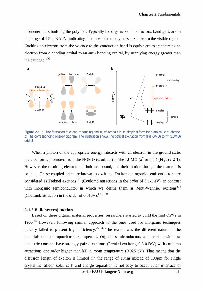
Chapter 2 Fundamentals
2016 FAU Erlangen-Nürnberg 31
monomer units building the polymer. Typically for organic semiconductors, band gaps are in
the range of 1.5 to 3.5 eV, indicating that most of the polymers are active in the visible region.
Exciting an electron from the valence to the conduction band is equivalent to transferring an
electron from a bonding orbital to an anti- bonding orbital, by supplying energy greater than
the bandgap.176
Figure 2-1: a) The formation of σ and π bonding and π, π* orbitals in its simplest form for a molecule of ehtene. b) The corresponding energy diagram. The illustration shows the optical excitation from π (HOMO) to π* (LUMO) orbitals.
When a photon of the appropriate energy interacts with an electron in the ground state,
the electron is promoted from the HOMO (π-orbital) to the LUMO (π*-orbital) (Figure 2-1).
However, the resulting electron and hole are bound, and their motion through the material is
coupled. These coupled pairs are known as excitons. Excitons in organic semiconductors are
considered as Freknel excitons177
(Coulomb attractions in the order of 0.1-1 eV), in contrast
with inorganic semiconductor in which we define them as Mott-Wannier excitons178
(Coulomb attraction in the order of 0.01eV).179, 180
2.1.2 Bulk heterojunction
Based on these organic material properties, researchers started to build the first OPVs in
1960.23
However, following similar approach to the ones used for inorganic techniques
quickly failed to present high efficiency.25, 26
The reason was the different nature of the
materials on their optoelctronic properties. Organic semiconductors as materials with low
dielectric constant have strongly paired excitons (Frenkel excitons, 0.3-0.5eV) with coulomb
attractions one order higher than kT in room temperature (0.025 eV). That means that the
diffusion length of exciton is limited (in the range of 10nm instead of 100μm for single
crystalline silicon solar cell) and charge separation is not easy to occur at an interface of
En
erg
ysp2
pz
σ*-orbital
π*-orbital
π-orbital
σ-orbizal
optical excitation
antibonding
bonding
C C
H
HH
H
120°
σ-bonding
π-bonding
C C C C
C C
pz-orbitals in phase
pz-orbitals out of phase
C C
π* orbital
π orbital
a b

Chapter 2 Fundamentals
32 2016 FAU Erlangen-Nürnberg
bilayer structure of n-type and p-type materials or polymer-fullerene heterojunctions.181-183
Thus, the question of efficient charge separation was not yet answered.
The bulk heterojunction concept solved this riddle and increased the yield of charge
separation and consecutively the efficiency of OSC. These advantages combined with the
process simplicity made it famous. Solution blends of p-type and n-type semiconductors are
combined and coated to form thin films with intermixed phases (Figure 2-2). Thus,
photogenerated excitons could find now in vicinity (<50nm) an interface to separate.
Figure 2-2: Bilayer vs bulk heterojunction structures. The exciton separation occurs at interfaces. Bulk heterojunction is more efficient because of the limited exciton diffusion length in organic materials. Reproduced with permission.184
-Operating Principles
A really useful generic description of the operating principles of bulk heterojunction
organic solar cells was presented by Carsten Deibel and Vladimir Dyakonov back in 2010.183
The whole process was separated into the following six steps. When a photon with energy
higher than the bandgap is absorbed (mostly by donor material), a singlet exciton is generated
Figure 2-3(i). The exciton will diffuse to a donor-acceptor interface Figure 2-3(ii) in order to
get dissociated-electron transfer in the acceptor molecule Figure 2-3 (iii). At this state the
electron-hole pairs are still Coulomb bound but in two different materials. The electron is in
the acceptor material forming a negative polaron and the hole remains on a donor material
forming a positive polaron. This Coulomb-bound polaron pair (also called charge transfer
state) has energy lower than exciton’s energy and it is the intermediate step before the
separation of charges. After dissociation, the electron-hole pair is separated by the build in
electric field (Figure 2-3(iv)) to free charges which they are transported to respective contacts
(Figure 2-3(v)). At the contacts the charges are extracted and photocurrent is produced

Chapter 2 Fundamentals
2016 FAU Erlangen-Nürnberg 33
(Figure 2-3(vi)). It is worthwhile to notice that exciton generation can occur at acceptor
material also. In that case a corresponding procedure for the holes is followed.
Figure 2-3: Operating principles of bulk heterojunction solar cell. Left: Simplified kinetics diagram. Right: Simplified energy diagram.(i) Singlet exciton generation. (ii) Exciton diffusion. (iii) Exciton dissociation. (iv) Charge separation. (v) Charge transport. (vi) Charge extraction. Reproduced with permission.183
-Charge Transfer state (CT)
The charge transfer (CT) state, also known as polaron pair, is the very important
intermediate step between exciton dissociation and charge separation. It plays a crucial role
on organic bulk heterojunction devices as it determines both open circuit voltage and
photocurrent.185
Indeed, recent practical estimations of efficiency limits for single bulk-
heterojunction organic solar cells have incorporated losses associated with CT state (sub-
chapter 2.6.1 ). Thus, it is worthwhile to zoom in the previous generic operating principles
diagram and understand the role of the CT state in the whole operation of photocurrent
generation.
Figure 2-4 shows the energy levels relevant to charge generation, dissociation, separation
and recombination in a donor-acceptor system. An incident photon with energy higher than
the optical band gap (here presented as Eabs) is absorbed and an electron is excited (S0-S1
transition) to form a strongly bound singlet exciton in the donor material (Figure 2-4 (i),(ii)).
The exciton will diffuse in order to find a donor-acceptor interface and dissociate (Figure 2-4
(iii)). In case of absence of acceptor molecule in the vicinity (in the range of ~10nm,but
strongly depending on the materials system) the singlet will recombine radiatively. Otherwise,
dissociation will occur with a charge transfer if it is energetically favorable, meaning that the
singlet exciton energy (Eabs) is higher than the CT state energy (ECT). In this case the CT state
will be populated. At this stage, if the coulomb binding energy (lower than Frenkel exciton

Chapter 2 Fundamentals
34 2016 FAU Erlangen-Nürnberg
binding energy) of the polaron pair is overcome, the pair separates into free charges (Figure
2-4 (iv)). If this is not the case, recombination of the charges can occur.183
Figure 2-4: Energy levels present in a donor–acceptor system which are relevant to the mechanisms of generation, recombination and dissociation of CT complexes. Reproduced with permission183
Polaron pair can recombine radiatively or non-radiatively; with direct transition to the
ground state or through a back transfer of the electron to a singlet or triplet state. These
oppositely charged polarons can originate from the same S0-S1 transition (geminate) or they
can be formed independently (non-geminate).183
It is worth highlighting that every transition
that leads to charge separation or recombination processes occurs under a probability that
depends on the energy difference between the initial and the final state. For organic solar cells
it has been shown that an ECT lower by 100meV from Eabs is close to optimum for driving a
separation process without inducing other losses.186, 187
On the recombination side, when a
triplet state energy is lower than CT state energy (ΔE≥100meV)186
, then most probably charge
recombination will occur via transition of the electron to the triplet state. These traps should
be avoided as they can diminish photocurrent and open circuit voltage leading to poor solar
cell performance.

Chapter 2 Fundamentals
2016 FAU Erlangen-Nürnberg 35
2.2 The theory behind perovskite solar cells
In this sub-chapter I will give a brief overview of the basic theoretical background behind
perovskite solar cells. The main building blocks and the key characteristics of this technology
are presented.
2.2.1 Perovskite light absorbers
The heart of a perovskite solar cell is an active layer based on organo-metal
semiconductor materials that follow the formula ABX3; where A is an organic cation, B a
small inorganic cation and X a halogen anion. The resulting crystal structure is illustrated in
Figure 2-5a. Their formability can be estimated by Goldschmidt’s tolerance factor (t) and the
octahedral factor (μ). In perovskites, the Goldschmidt’s tolerance factor is the ratio between
A-X and B-X distances, considering molecules as ideal hard spheres:
where rA , rX, rB are the effective ionic radii of A, X, B. While the octahedral factor is given
by:
For halide perovskites is generally expected 0.813 < t < 1.107 and 0.44 < μ < 0.90 however
for high symmetry cubic structures the window of t becomes smaller (0.89-1.0 with the
highest symmetry demonstrated for highest t values).51, 188
By solving those equations for radii of various molecules and atoms of the A,B,X groups
scientists can study the crystallographic stability of each combination. It has been found that
organic cations with radii between 0.16-0.25 nm are forming stable crystal structures.
Therefore cations such as methylamonium (CH3NH3+, rA = 0.18nm), ethylamonium
(CH3CH2NH3+, rA = 0.23 nm) are giving promising results. As a halogen anion X chloride (Cl
-
), bromide(Br-) or iodide (I
-) are commonly used with 0.181 nm, 0.196 nm and 0.220 nm radii
correspondingly. Traditionally, for the inorganic cation B, Pb (rB = 0.119 nm) or Sn (rB =
0.110 nm)-for lead-free but less stable perovskite solar cells- have prevail. In total, the most
studied perovskite system is methylamonium lead trihalide (CH3NH3PbX3) with a tunable
optical bandgap between 1.5 eV (CH3NH3PbI3) and 2.3 eV (CH3NH3PbBr3) depending on the
halide anion.51, 188
𝑡 =(𝑟𝐴+𝑟𝑋)
√2(𝑟𝐵+𝑟𝑋)
𝜇 =𝑟𝐵
𝑟𝑋

Chapter 2 Fundamentals
36 2016 FAU Erlangen-Nürnberg
Figure 2-5: a) Perovskite crystal structure of the form ABX3. b) The energy diagram of CH3NH3PbI3 perovskite resulted from the antibonding orbitals of the bonds between Pb (B) and I (X). The illustration shows the optical excitation highest occupied state to the lowest unoccupied state.
-Energy Band structure
Long time before the explosion of the perovskite field, Umebayashi et. al presented
useful insight on the energy band structure of perovskite crystals.189
By investigating 3D
crystals CH3NH3PbI3 and 2D crystals (C4H9NH3)2PbI4 they found that they are
semiconductors with a direct band gap at the R and Γ points respectively. Interestingly, the
band formation is only due to antibonding orbitals. Indeed, for the 3D crystal CH3NH3PbI3 ;
the highest occupied states (or top of the valence band) consists of the Pb 6s- I 5p σ-
antibonding orbital, while the lowest unoccupied state (or bottom of the conduction band)
consists of Pb 6p- I 5s σ-antibonding and Pb 6p- I 5p π-antibonding orbitals Figure 2-5b.
This investigation even though very informative it was simplistic and would give general
information as the authors did not take spin orbit interactions into account.190
More recently,
Even et. al. showed that spin splits in the highest occupied states would decrease the
theoretical band gap close to the experimentally observed values.191
It is worth highlighting the ease of band gap tuning in perovskite absorbers as it can have
great impact in optoelectronic devices. Great changes in band gap (from ~1.5 to ~2.3eV) have
been reported mainly by substituting the halogen anion or by using a mixed halide
composition. For example Sadhanala et al. demonstrated a bromide-iodide lead perovskite
film with a tunable band gap between the extremes of pure iodide (2.23V) and bromide
(1.57V) perovskites.192
One year later they showed similar tuning for bromide-chloride
perovskite films with tunable band gap between ~3.1 to 2.3eV.193
Alternatively, band gap
A
B
X
Ene
rgy
Pb 6s – I 5p *
Pb 6p – I 5p *
Pb 6p – I 5s *
Efoptical excitation
0D 3Dba

Chapter 2 Fundamentals
2016 FAU Erlangen-Nürnberg 37
tuning has been reported by changing the organic cation, e.g. methylamonium to
formamidinium.194, 195
-Charge Transport
Perovskite films combine high absorption coefficient and balanced charge transport
behavior that ensures high efficiency cells. In 2013 Xing et. al and Stranks et al. investigated
the electron and hole diffusion length for CH3NH3PbI3 (presented by both groups) and
CH3NH3PbI3-xClx (presented from Stranks et. al).196, 197
For CH3NH3PbI3 films the electron
and hole diffusion length were found at ~130nm and ~100nm correspondingly. Nevertheless,
for CH3NH3PbI3-xClx films the diffusion lengths were even larger, with the remarkable values
of ~1069nm and ~1213nm for electron and hole respectively. These extremely large balanced
values –which indicate weakly bound excitons- in combination with high absorption
coefficient ( ~104-10
5cm
-1)
51 ensure sufficient photocurrent generation and charge extraction
in a solar cell based on perovskite absorber.
-Perovskite solar cell structure
The solar cell structure of devices employing perovskite absorber layers evolved over
time leading to the high efficiency perovskite solar cells of today.188
Since a state of the art
with the efficiency rising has been presented earlier (sub-chapter 1.2.2 ) here I will focus on
presenting the structural evolution. Initially, perovskite absorber was used as a sensitizer in a
dye-sensitized solar cell concept substituting the molecular dye (Figure 2-6a). In this concept,
a mesoporous oxide layer (e.g TiO2) forms a scaffold and perovskite is absorbed on the
interfaces, finally the whole structure is covered by an HTM. Here the oxide layer is used as
an electron acceptor and the HTM as a hole acceptor layer with a perovskite dye in their
interface to conclude a heterojunction. Later, a similar approach but with a non-injecting
scaffold (electron injection from perovskite to Al2O3 was prohibited) was followed to lead on
the first indication that electron transfer was possible in perovskite absorber and consequently
the dye-sensitized concept was not necessary (Figure 2-6b). After that a mesoporous structure
of TiO2 was infiltrated solely with perovskite absorber and the structure was concluded with a
thin layer of HTM on top (Figure 2-6c). Finally, a planar structure with p-i-n heterojunction
achieved high efficiency. Here the perovskite film would be the intrinsic layer, the HTM the
p-type layer and the oxide film (TiO2) the n-type layer. PEDOT:PSS and spiro-OMeTAD are
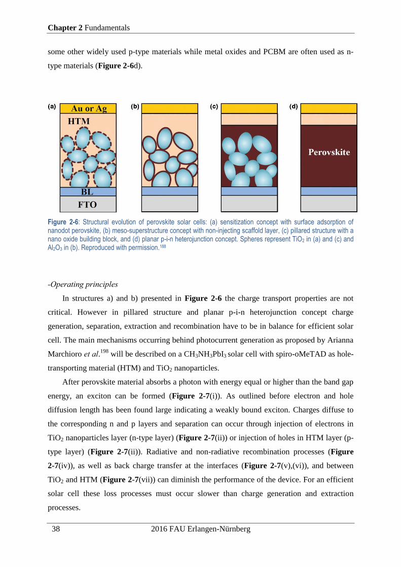
Chapter 2 Fundamentals
38 2016 FAU Erlangen-Nürnberg
some other widely used p-type materials while metal oxides and PCBM are often used as n-
type materials (Figure 2-6d).
Figure 2-6: Structural evolution of perovskite solar cells: (a) sensitization concept with surface adsorption of nanodot perovskite, (b) meso-superstructure concept with non-injecting scaffold layer, (c) pillared structure with a nano oxide building block, and (d) planar p-i-n heterojunction concept. Spheres represent TiO2 in (a) and (c) and Al2O3 in (b). Reproduced with permission.188
-Operating principles
In structures a) and b) presented in Figure 2-6 the charge transport properties are not
critical. However in pillared structure and planar p-i-n heterojunction concept charge
generation, separation, extraction and recombination have to be in balance for efficient solar
cell. The main mechanisms occurring behind photocurrent generation as proposed by Arianna
Marchioro et al.198 will be described on a CH3NH3PbI3 solar cell with spiro-oMeTAD as hole-
transporting material (HTM) and TiO2 nanoparticles.
After perovskite material absorbs a photon with energy equal or higher than the band gap
energy, an exciton can be formed (Figure 2-7(i)). As outlined before electron and hole
diffusion length has been found large indicating a weakly bound exciton. Charges diffuse to
the corresponding n and p layers and separation can occur through injection of electrons in
TiO2 nanoparticles layer (n-type layer) (Figure 2-7(ii)) or injection of holes in HTM layer (p-
type layer) (Figure 2-7(ii)). Radiative and non-radiative recombination processes (Figure
2-7(iv)), as well as back charge transfer at the interfaces (Figure 2-7(v),(vi)), and between
TiO2 and HTM (Figure 2-7(vii)) can diminish the performance of the device. For an efficient
solar cell these loss processes must occur slower than charge generation and extraction
processes.

Chapter 2 Fundamentals
2016 FAU Erlangen-Nürnberg 39
Figure 2-7: Schematic illustration of energy levels and processes in a perovskite solar cell employing TiO2 and an HTM.
2.3 Device architectures
OPVs, perovskites and tandem solar cells can be fabricated in normal or inverted
architectures. The names normal and inverted are nothing but a convention among the PV
community and they refer to the fabrication sequence of the device. For different architectures
different electrodes or buffer layers may be used and the photogenerated current travels to
opposite directions. Inverted architectures traditionally show higher stability and they are
extensively used through this thesis. Figure 2-8 illustrates normal and inverted architectures
for single junction and tandem solar cells.
Devices can be developed on various substrates with mechanical properties coherent to
the fabrication route and the utility of the final product. Glass and polyethylene terephthalate
(PET) substrates are the most used, but more exotic substrates have been also reported.17, 18,
199, 200. For solar cells and other optoelectronics, at least one of the electrodes should show
high transparency. The most widely used transparent electrode is ITO but it presents
tremendous disadvantages (the readers are addressed to sub-chapter 1.3 ). If transparency for
the whole device is not a requirement then a metal (usually Ag for inverted and Al for normal
structure due to work function appropriateness) usually forms the second electrode.
Ene
rgy
TiO2 Perovskite HTM
hν
(i)
(ii)
(iii)
(iv)(v)
(vi)(vii)

Chapter 2 Fundamentals
40 2016 FAU Erlangen-Nürnberg
Alternative electrodes have been discussed earlier (sub-chapter 1.3 ). The important
correlation between transparency and sheet resistance will be discussed in the next section.
Figure 2-8: Normal architecture for single junction (a) and tandem solar cell (c). Inverted architecture of single junction (b) and tandem solar cells (d).
In solution processed solar cells, the most commonly used hole transport layer (HTL) is
PEDOT:PSS. However, solution processed metal oxides such as V2O5, WO3 or MoO3 have
been also reported efficient.201-203
Alternatively, if solution processability is not a requirement
thermal evaporation of MoO3 is frequent. As electron transport layers (ETLs) n-type metal
oxides (such as ZnO and TiOX) and polymer electrolytes (such as PFN,CPE and PEIE) have
been reported for equally high performance.204-209
While for normal architecture thermal
evaporated LiF and Ca are used. It is worthwhile to notice that additional modifying layers for
HTLs and ETLs have been frequently reported to improve the extraction of carriers.210
ba
c d

Chapter 2 Fundamentals
2016 FAU Erlangen-Nürnberg 41
2.4 Electrodes
In general, when it comes to the performance evaluation of a semi-transparent electrode,
two major aspects have to be linked; the transmittance (T) and the sheet resistance (Rsheet).
Typically, high transmittance can be achieved by reducing the thickness of the electrode.
However, this usually also leads to decreased conductivity. The challenge becomes clear;
materials that exhibit high conductivity combined with low thickness- high transmittance with
low sheet resistance- must be employed.
Several experimental studies have been conducted to show the T vs Rsheet correlation.
Based on them, useful figure of merits (FOMs) that link these two values can been
extracted.133, 211
Expressing transmittance as function of thickness (t), for a film thinner that
the wavelength of light, we end up with the following equation:
where Z0 is the impedance of free space (~376.73 Ω) and σop the optical conductivity (a
fundamental property of the material that is related to the absorption coefficient α through
σop α/ Z0). Sheet resistance as function of thickness can be expressed as follows:
where σDC,B is the DC bulk conductivity of the film. Then by combining equation 2.2 and 2.1
we obtain a relationship between T and Rsheet:
Usually, the ratio σDC,B/ σop is used as one useful FOM to describe the T vs Rsheet of a given
film. For higher values of the ratio, a film can achieve higher transmittance for lower sheet
resistance. To get an indication of the order of magnitude of this number it is worth
mentioning that σDC,B/ σop ≥35 is required to reach T≥90% with Rsheet≤100 Ω/sq.
However, fits to experimental data of T vs Rsheet have shown that very thin layers with
high transmittance (T>50-90%, depending on the material) do not follow a trend described
from equation 2.3. This deviation was explained with percolation effects. According to the
percolation theory the conductivity (σDC) of a thin spread inhomogeneous network of
conductive pathways (such as a thin semitransparent electrode of silver nanowires) should be
𝑇 = (1 +𝑍0
2𝜎𝑜𝑝𝑡)
−2 (2.1)
𝑅𝑠ℎ𝑒𝑒𝑡 = (𝜎𝐷𝐶,𝐵𝑡)−1
(2.2)
𝑇 = (1 +𝑍0
2𝑅𝑠ℎ𝑒𝑒𝑡
𝜎𝑜𝑝
𝜎𝐷𝐶,𝐵)−2
(2.3)

Chapter 2 Fundamentals
42 2016 FAU Erlangen-Nürnberg
described by a formula that includes a critical thickness (threshold thickness of the film)
associated with the percolation threshold:
where n is the percolation exponent. For a network with high enough conductivity (t >>tc)
equation 2.4 can be changed to:
where tmin is the thickness at which σDC,B = σDC . Now a new description of sheet resistance of
the film for this regime would be:
then by solving 2.6 for t and combining with 2.1 we obtain:
where Π is the percolative FOM:
is worth noticing that for n=0 we go back to the equation 2.3 as it is also defined from σDC.
Taking a closer look to the final equations, we see that the ratio σDC,B/ σop is inside the
percolative FOM but does not control it as previously. In general, a film that shows high Π
values combines high T with low Rsheet.
The semi-transparent solution processed electrodes with high potential were introduced
earlier in sub-chapter 1.3 Graphene, carbon nanotubes (CNTs), conductive polymers, metal
grids and metal nanowires (NWs) have been proven promising as ITO substitutes in solar cell
architectures. Figure 2-9 shows the T as a function of Rsheet for the most famous choices. It is
worth noticing that for solution processed electrodes the highest values for the σDC,B/ σop FOM
have been reached by metallic NWs electrodes (σDC,B/ σop =106-453) and the lowest by
graphene only electrodes (σDC,B/ σop 1.3). 133
𝜎𝐷𝐶 ∝ (𝑡 − 𝑡𝑐)𝑛 (2.4)
𝜎𝐷𝐶 = 𝜎𝐷𝐶,𝐵 (𝑡
𝑡𝑚𝑖𝑛)𝑛
(2.5)
𝑅𝑠ℎ𝑒𝑒𝑡 = (𝜎𝐷𝐶𝑡)−1 = [𝜎𝐷𝐶,𝐵 (
𝑡
𝑡𝑚𝑖𝑛)𝑛𝑡]−1
= (𝑡𝑚𝑖𝑛
𝑛+1
𝑡𝑚𝑖𝑛𝜎𝐷𝐶,𝐵𝑡𝑛+1) (2.6)
𝑇 = [1 +1
𝛱(
𝑍0
𝑅𝑠ℎ𝑒𝑒𝑡)1 (𝑛+1)⁄
]−2
(2.7)
𝛱 = 2 [𝜎𝐷𝐶,𝐵 𝜎𝑜𝑝⁄
(𝑍0𝑡𝑚𝑖𝑛𝜎𝑜𝑝)𝑛]1 (𝑛+1)⁄
(2.8)

Chapter 2 Fundamentals
2016 FAU Erlangen-Nürnberg 43
Figure 2-9: Transmittance versus sheet resistance for promising solution processed electrodes.164, 212-214 Transmittance values were obtained at ~550nm. The bulk regime (described by equation 2.3) is shown with solid line. The percolation regime (described by equation 2.7) is shown with dashed line.133
2.5 Current-voltage characteristics and diode equation
-Current-voltage characteristics
The most important characteristics of a solar cell can be extracted from a current (or
current density) versus voltage curve under dark and illuminated conditions (Figure 2-10).
Figure 2-10: a) Linear and b) semi-logarithmic presentation of J-V curves und dark and illuminated conditions. Reproduced with permission.183
a b

Chapter 2 Fundamentals
44 2016 FAU Erlangen-Nürnberg
The measurement occurs by recording the current of the device while a range of voltages is
scanned, usually at room temperature and under specified illumination or in the dark. The
parameters that determine the power conversion efficiency (PCE) and can be extracted from a
J-V curve under illumination are :
o Open circuit voltage (Voc), as its name reveals, is the applied voltage at which the
current density equals to 0. At this point the diode is open and no current flows
through the device
o Short circuit current density (Jsc) is the current density of the device when the applied
voltage equals to 0.
o Maximum power point (MPP) is the point between short-circuit and open-circuit
conditions at which the generated power (P = V x I) reaches the highest value. At this
point V=VMPP and I=IMPP.
o Fill Factor (FF) is the ratio between MPP and the product of Jsc and Voc and is
described by the following formula
o Then, the power conversion efficiency (PCE) of a solar cell is described as:
-Shockley-diode equation
In 1961 Shockley and Queisser estimated the efficiency limits (sub-chapter 2.6 ) for inorganic
solar cells by using the famous Shockley-diode equation. Shockley-diode equation models a
solar cell simply as a parallel connection of a photocurrent generator and a diode. Thus, in the
dark the net current density (J) at a given voltage (V) for an ideal solar cell is given by:
where Jo is the dark saturation current density of the diode, q is the elementary charge, n the
diode ideality factor, k the Boltzman constant and T the temperature (kT describes the thermal
energy). Under illumination the two components generate a current with opposite directions
and the equation changes to:
𝐹𝐹 =𝑉𝑀𝑃𝑃×𝐼𝑀𝑃𝑃
𝑉𝑜𝑐×𝐼𝑠𝑐 (2.9)
𝑃𝐶𝐸 =𝑃𝑜𝑢𝑡
𝑃𝑖𝑛=
𝐹𝐹×𝑉𝑜𝑐×𝐼𝑠𝑐
𝑃𝑖𝑛 (2.10)
𝐽 = 𝐽0 [𝑒𝑥𝑝 (𝑞𝑉
𝑛𝑘𝑇) − 1] (2.11)
𝐽 = 𝐽0 [𝑒𝑥𝑝 (𝑞𝑉
𝑛𝑘𝑇) − 1] − 𝐽𝑠𝑐 (2.12)

Chapter 2 Fundamentals
2016 FAU Erlangen-Nürnberg 45
By solving the equation for J=0 we find the correlation of Voc with the diode and
photogenerator characteristics:
Although a good first approximation the above mentioned equations refers to an ideal solar
cell. In order to describe the J-V behavior of a real solar cell, two resistance elements were
introduced in the ideal Shockley-diode equation. The series resistance (Rs), which is
electrically connected is series with the diode (Figure 2-11), describes charge transport
resistances (contact resistances, injection barriers, sheet resistances etc.). The parallel or shunt
resistance (Rp), which is electrically connected in parallel with the photodiode, describes
shunts between two electrodes and every current flow pathway that bypasses the diode. Thus,
the equation now becomes:
where Jph the optional photocurrent density (shift of J-V under illumination, ~ Jsc). An
efficient system would demonstrate minimized Rs and maximized Rp. These elements can be
extracted from semi logarithmic representation of J-V graphs under dark and illuminated
conditions (Figure 2-10b).
Figure 2-11: Single diode equivalent circuit model commonly employed in estimating electrical losses in solar cell.
Rp
Rs
hνV
+
-
J
Jph
𝑉𝑜𝑐 =𝑛𝑘𝑇
𝑞ln (
𝐽𝑠𝑐
𝐽0+ 1) (2.13)
𝐽 = 𝐽0 [𝑒𝑥𝑝 (𝑞(𝑉−𝐽×𝑅𝑠)
𝑛𝑘𝑇) − 1] −
𝑉−𝐽×𝑅𝑠
𝑅𝑝− 𝐽𝑝ℎ (2.14)

Chapter 2 Fundamentals
46 2016 FAU Erlangen-Nürnberg
2.6 Efficiency limits of solar cells
What is the efficiency limit of a solar cell? This question is one of the most fundamental
and perhaps vital questions in the field. Not only because it reveals the boundaries of solar
technology but also because it gives us hints on how to circumvent those boundaries. One of
the most famous examples of fighting those boundaries, the multi-junction (or tandem)
concept, has its roots on the deep understanding of the fundamental problems. In the next sub-
chapters all these are discussed.
2.6.1 Shockley-Queisser limit for single junction solar cells
Back in 1961, William Shockley and Hans-Joachim Queisser make one very significant
contribution to the field of solar energy. They calculated the maximum theoretical conversion
efficiency (detailed balance limit) of inorganic single p-n junction solar cells by assuming
several hypothesis and mechanisms based on thermodynamic phenomena.215
The main
hypothesis were;
i) Only photons with higher energy than the bandgap (hvg > Eg) could be absorbed
and contribute in photocurrent generation (step function). Photons with higher
energy than the bandgap would excite charge carriers in higher states than Ec.
These hot carriers would then relax through thermalization process to Ec.
ii) Only radiative recombination occurs (loss mechanism). Cell is assumed to radiate
as an ideal black body with temperature of 300°K. Sun is assumed to radiate as an
ideal black body with a temperature of 6000°K.
iii) Each photon absorbed produces an electron that eventually will be extracted,
meaning IQE values of 100%.
-Ultimate efficiency limit
According to these assumptions and since radiative recombination was assumed the only
loss mechanism, they first calculated the ideal ultimate efficiency of a circular cell with a T=
0°K. For the ideal black body behavior that means that no recombination occurs. The cell was
surrounded by a cavity which was emitting at a T=Ts=6000°K (corresponding to sun). Then
the efficiency would be
𝜂 = 𝑔𝑒𝑛𝑒𝑟𝑎𝑡𝑒𝑑 𝑝ℎ𝑜𝑡𝑜𝑛 𝑒𝑛𝑒𝑟𝑔𝑦
𝑖𝑛𝑝𝑢𝑡 𝑒𝑛𝑒𝑟𝑔𝑦=
ℎ𝑣𝑔𝑄𝑠
𝑃𝑠 (2.15)

Chapter 2 Fundamentals
2016 FAU Erlangen-Nürnberg 47
where hvg is the energy of a photon required to be absorbed, Qs the number of photons
absorbed and Ps is the input energy containing the spectrum. By using the Plank’s law which
gives the spectral photon flux (ϕ) as a function of wavelength (or frequency, v) and the
temperature of the black body (T):
they calculated Qs and Ps as follows :
where xg is given by
corresponding to the energy of the band gap.
Then eventually by substituting equations 2.18 and 2.16 in 2.15 they found that an ideal
ultimate efficiency of ~44% for a material with a band gap of ~1.08eV. However this
efficiency is far from a realistic scenario since no losses were assumed.
-Realistic efficiency limit
In a more realistic approach, the radiative recombination losses as well as a rectangular
architecture of a solar cell was taken into account. Due to the rectangular architecture the
number of photons absorbed (Qs) was changed by a geometrical factor. To estimate the
radiative recombination losses, they assumed that a cell at a temperature of 300°K is
surrounded by a cavity of an equal temperature (which corresponds to dark ambient). No
voltage is applied to the cell, thus the whole system is in thermodynamic equilibrium. That
means that the radiation absorbed by the cell equals to the radiation emitted by the cell which
results completely from radiative recombination as was hypothesized. Then the radiation
absorbed which equals to the radiation from radiative recombination (RRR ) at V=0 would be:
𝜙(𝑣, 𝑇) =2ℎ𝑣3
𝑐21
𝑒
ℎ𝑣𝑘𝐵𝑇−1
(2.16)
𝑄𝑠 ≡ 𝑄(𝑣𝑔, 𝑇𝑠) =2𝜋
𝑐2∫
𝑣2𝑑𝑣
𝑒ℎ𝑣𝑘𝑇𝑠−1
=2𝜋(𝑘𝑇𝑠)
3
ℎ3𝑐2∫
𝑥2𝑑𝑥
𝑒𝑥−1
∞
𝑥𝑔
∞
𝑣𝑔 (2.17)
𝑥𝑔𝑘𝑇𝑠 = ℎ𝑣𝑔 = 𝑞𝑉𝑔
𝑃𝑠 =2𝜋
𝑐2∫
𝑣2𝑑𝑣
𝑒ℎ𝑣𝑘𝑇𝑠−1
=∞
0
2𝜋(𝑘𝑇𝑠)4
ℎ3𝑐2∫
𝑥3𝑑𝑥
𝑒𝑥−1
∞
0 (2.18)

Chapter 2 Fundamentals
48 2016 FAU Erlangen-Nürnberg
where A is the area of the cell and Qc is the number of photons absorbed by the cell:
To find the RRR for V≠0 they utilized pn junction theory as follows. If V=0 then:
where n denotes the number of elections and p the number of holes and the indicator the
voltage. If V≠0 then the rate of radiative recombination becomes:
then according to equation 2.19 the main loss mechanism would be described by:
By knowing the amount of absorbed photons Qs, the amount of recombined emitted photons
Qc and the general correlation of the rate of recombination and the applied voltage, they end
up with a current voltage relationship (which is of the same form as the famous Shockley
diode equation, equation 2.12):
where the second term
is independent of voltage. And the first term includes the loss mechanism.
The efficiency of a solar cell can be described also as:
Then by including following equation 2.25 the authors plot the η as a function of xg
(which corresponds to the band gap of the material) to find out a maximum efficiency of
~30% for an energy band gap of 1.1eV. 215
𝑅𝑅𝑅,𝑉=0 = 2𝐴 𝑄𝑐 (2.19)
𝑄𝑐 = 𝑄(𝑣𝑔, 𝑇𝑐) =2𝜋(𝑘𝑇𝑐)
3
ℎ3𝑐2∫
𝑥2𝑑𝑥
𝑒𝑥−1
∞
𝑥𝑔 𝑥𝑐⁄ (2.20)
𝑅𝑅𝑅 = 2𝐴 𝑄𝑐𝑒𝑞𝑉
𝑘𝑇 (2.23)
𝐽 = 𝐽0 [𝑒𝑥𝑝 (𝑞𝑉
𝑛𝑘𝑇) − 1] − 𝐽𝑠𝑐 (2.24)
𝐽𝑠𝑐 ∝ 𝑞(𝑄𝑠 − 𝑄𝑐) (2.25)
𝜂 = 𝑃𝑚𝑎𝑥
𝑃𝑖𝑛=
max(𝐽𝑉)
𝑃𝑖𝑛 (2.26)
𝑅𝑅𝑅,𝑉=0 ∝ 𝑛0𝑝0 (2.21)
𝑅𝑅𝑅,𝑉≠0 ∝ 𝑛𝑝 = 𝑛0𝑝0𝑒𝑞𝑉
𝑘𝑇 (2.22)

Chapter 2 Fundamentals
2016 FAU Erlangen-Nürnberg 49
-Useful equivalent formulas
The phenomena introduced above can be equally described by equivalent formulas which
in some cases are more practical (see next sections). The efficiency of a solar cell
incorporating semiconductor with band gap energy of Eg can be equally described as :
which is the same equation we practically use when measuring current-voltage
characteristics (eub-chapter 2.5 ). Jsc can be expressed as:
where for a step function as assumed in SQ theory α(E) is zero for E<Eg and the
boundaries of the integral can be changed from Eg to ∞. Or equally expressed:
and
where ϕsun is the spectral photon flux density of the sun incident on flat surface, ϕbb is
the spectral flux density emitted by a black body at temperature T ( the environment, which in
case of SQ theory since all recombination processes are radiative it also corresponds to the
spectral flux density emitted by the cell).46
For a more realistic approach where the
recombination processes are not only radiative, Rau showed that a reciprocal relationship
between quantum efficiency of electroluminescence (EQEEL) and external quantum efficiency
(EQE) exists :216
then a practical dark saturation current J0 can be described as function of EQEEL and EQE :
𝜂 =𝐽𝑠𝑐𝑉𝑜𝑐𝐹𝐹
𝑃𝑖𝑛 (2.27)
𝐽𝑠𝑐 = 𝑞 ∫ (𝜙𝑠𝑢𝑛(𝐸) − 𝜙𝑏𝑏(𝐸))𝑎(𝐸)𝑑𝐸∞
0 (2.28)
𝐽𝑠𝑐 = 𝑞 ∫ 𝜙𝑠𝑢𝑛(𝐸)𝐸𝑄𝐸(𝐸)𝑑𝐸∞
0 (2.29)
𝐽0 = 𝑞 ∫ 𝜙𝑏𝑏(𝐸)𝑎(𝐸)𝑑𝐸∞
0 (2.30)
𝐽0 =𝑞
𝐸𝑄𝐸𝐸𝐿∫ 𝐸𝑄𝐸(𝐸)𝜙𝑏𝑏(𝐸)𝑎(𝐸)𝑑𝐸∞
0 (2.32)
𝐸𝑄𝐸𝐸𝐿(𝐸) = 𝐸𝑄𝐸(𝐸)𝜙𝑏𝑏(𝐸) [𝑒𝑥𝑝 (𝑞𝑉
𝑛𝑘𝑇) − 1] (2.31)

Chapter 2 Fundamentals
50 2016 FAU Erlangen-Nürnberg
2.6.2 Efficiency limits in single-junction organic solar cell
The SQ theory can be applied to organic solar cells basically with a main extension;
charge separation in bulk heterojunction occurs through a CT state and these states determine
Voc losses. Even though ideal materials such the ones described for SQ theory are far from
organics, the OPV community used it as useful tool to extract semi-empirical theoretical
limits. This is beneficial for the community as losses were identified and new design rules for
creating novel materials (appropriate band gap and HOMO levels to increase and efficiency
and Voc ) and device architectures were used to circumvent them.
In 2006, Scharber et al. predicted for the first time the power conversion efficiency limit
for bulk-heterojunction solar cells based on conjugated donor polymer and PCBM
acceptors.217
The maximum limit was found to be ~11% after several empirical estimates.
Initially, the Voc is reduced due to the lowest difference between the LUMO levels of donor
and acceptor that efficient charge separation would occur (as set by the authors, ΔLUMO >
0.3eV) (Figure 2-12b). Additionally it has been empirically proven that Voc is not the exact
difference between donor’s HOMO and acceptor’s LUMO but reduced by an additional factor
of 0.3eV:
On top of those fundamental losses, Scharber et al. assumed charge carrier transport losses
(FF = 65%) and a constant EQE of 65% which brought the limit to its final value. These
values for EQE and FF were chosen according to the best experimental values of the time.
During the following years Koster et al.218 , Minnaert et al.219
and Lunt et al.229 followed
approaches where they assumed different values for Jsc, EQE , FF, Voc and ΔLUMO to
predict a realistic limit close to what presented from Scharber et al. Meanwhile, continuous
development of novel materials led to more efficient devices with higher FFs and EQE values.
In 2011 Lunt et al. assuming that the Voc of single junction nanostructured devices could
reach 80% of the SQ limit, and 75% for both EQE and FF he estimated an practical limit of
17%. While, in 2013 Scharber et al. updated his older prediction to find an achievable PCE of
15%, assuming a FF of 75% and a constant EQE of 80% (Figure 2-12a).220
𝑉𝑜𝑐 =1
𝑒(|𝐸𝐻𝑂𝑀𝑂
𝐷 | − |𝐸𝐿𝑈𝑀𝑂𝐴 |) −0.3V (2.33)

Chapter 2 Fundamentals
2016 FAU Erlangen-Nürnberg 51
Figure 2-12: a) PCE prediction of a bulk heterojunction solar cell with PCBM as acceptor material. For the calculation Scharber et al. assumed FF of 75%, EQE of 80% and Voc according to Eq.2.13. b) Simplified energy diagram of a donor acceptor system. Reproduced with permission.220
Although good practical estimations of the efficiency limit for the organic solar cells, the
aforementioned approaches do not include the influence of the CT state (sub-chapter 2.1.2 ) in
Voc. Since 2008, Vandewal et al. had already observed experimentally the CT state by
measuring EQE with the high sensitive Fourier-transform photocurrent spectroscopy (FTPS),
and given a first estimation about the losses induced in Voc.221
In consistence with Vandewal
et al., in 2009 Veldman et al. by studying several donor and acceptor materials he obtained
the following relation between Voc and ECT :
Additionally, the authors experimentally showed that energy difference of 100meV between
Eg and ECT is sufficient for charge transfer.186
That would mean that Eg - qVoc 0.6eV. With
these observations in hand and with similar assumptions to the first estimation of maximum
efficiency from Scharber et al. (65% for EQE and FF) Valdeman et al. presented a maximum
efficiency of 11% for bulk heterojunction systems when the lowest optical band bap (Eg)
values lies between 1.37-1.45 eV (Figure 2-13).
a b
𝑞𝑉𝑜𝑐 = 𝐸𝐶𝑇 − 0.47(±0.06)𝑒𝑉 (2.34)

Chapter 2 Fundamentals
52 2016 FAU Erlangen-Nürnberg
Figure 2-13: Theoretical efficiency of bulk-heterojunction photovoltaic devices with Eg− qVoc= 0.60 eV (solid line) versus the lowest optical bandgap of the two materials, calculated using the AM1.5 spectrum, FF = 0.65, and assuming constant EQE = 0.65 between 3.5 eV and Eg . The dashed lines show the theoretical efficiencies for devices using the larger Eg − qV oc offsets for (from top to bottom): PF10TBT:[60]PCBM (0.70 eV,circles), PCPDTBT:[70]PCBM (0.76 eV, down triangles), PBBTDPP2:[70]PCBM (0.80 eV, up triangles), and P3HT:[60]PCBM (1.09 eV, squares). The closed markers represent the theoretical efficiency, the open markers the device efficiencies. Reproduced with permission. 186
Since then, further investigations on CT state gave new insight on the relation to Voc.
Specifically, Vanderwal et al. utilized effect of the reciprocal relationship by Rau in J0
(equation 2.32) and the Voc formula from Shockley diode equations (equation 2.13) to prove
that:
This formula emerges the three main factors determine the Voc and correlates them with
measurable properties.187, 222, 223
The first term (Ect/q) relates to the energy of the CT state.
The second term (𝑘𝑇
𝑞ln (
𝐽𝑠𝑐ℎ3𝑐2
𝑓𝑞2𝜋𝐸𝐶𝑇)) shows the radiative voltage losses and relates to the CT
absorption strength (𝑓) which results from the density of donor-acceptor contacts and donor-
acceptor electronic coupling. While the third term (𝑘𝑇
𝑞ln(𝐸𝑄𝐸𝐸𝐿)) describes the non-radiative
voltage losses and relates to EQEEL. With approximate values of ~0.25eV and ~0.35eV for the
second and third term respectively a new empirical approximation for VOC and ECT was given:
𝑞𝑉𝑜𝑐 = 𝐸𝐶𝑇 − 0.6𝑒𝑉 (2.36)
𝑉𝑜𝑐 ≈𝐸𝐶𝑇
𝑞+
𝑘𝑇
𝑞ln (
𝐽𝑠𝑐ℎ3𝑐2
𝑓𝑞2𝜋𝐸𝐶𝑇) +
𝑘𝑇
𝑞ln(𝐸𝑄𝐸𝐸𝐿) (2.35)

Chapter 2 Fundamentals
2016 FAU Erlangen-Nürnberg 53
Although very close to previous on presented by Veldman et al. the theory behind this
approximation gave important insight on radiative and non-radiative losses in organic solar
cells. It is worth highlighting that EQEEL which determines the non-radiative losses, is ~10-6
for organic solar cells and results in ~0.36V losses, while in inorganics is much lower.187
For
example crystalline Si solar cells show EQEEL~10-3
resulting in 0.18V losses, and GaAs solar
cells show EQEEL~10-2
resulting in 0.12V.224
Most recently, Scharber released a new update where he follows a similar approach to
the one presented in 2006 and 2013, but takes into account the CT state and VOC energy losses
of qVOC –Eg= 0.7eV.225
Assuming EQE and FF of 70% he demonstrated that to surpass a
maximum efficiency of ~12% the energy loss (qVOC –Eg ) should be limited to less than
0.7eV (Figure 2-14). However, the work of Li et al. in 2015 suggests that systems with
energy losses lower than 0.7eV are difficult to reach EQE values greater than 70%.226
Figure 2-14: Contour plot showing the calculated energy-conversion efficiency (contour lines and colors) versus the absorption onset and the HOMO level of the donor polymer according to ref. [217] assuming an EQE and a FF of 70%; Dots indicate the performance potential of the investigated polymers. Reproduced with permission. 225
2.6.3 Efficiency limits in single-junction perovskite solar cell
Similarly to organic solar cells, the SQ theory can be also applied to perovskite solar cells
by introducing the main losses of these devices. Additionally, perovskite solar cells exhibit
characteristics closer to the ideal case, making these predictions more realistic.197, 227
The
radiative and non-radiative recombination losses can be studied in open circuit condition and
,as shown in case of organics, they influence the maximum Voc.

Chapter 2 Fundamentals
54 2016 FAU Erlangen-Nürnberg
In 2014, Tvingstedt et al. followed a similar approach shown by Vandewal et al. (in
OPVs)187
to demonstrate the Voc losses in perovskites. Initially by using the reciprocity
relation between electroluminescence quantum efficiency (EQEEL) and the photovoltaic
quantum efficiency (EQE) described by Rau (equation 2.31) he expressed the dark saturation
current (J0) as:
where as described previously, the ϕbb is the spectral flux density of a black body that
irradiates at temperature, T (the environment). When a solar cell reaches the radiative limit
(meaning that all recombination processes are only radiative) the EQEEL=1 and J0:
In which if we assume also EQE=1 we go back to SQ theory.
Then by using the Shockley diode equation (equation 2.13) for the Voc the authors ended
up with the following expression:
With a close look on that equation we can see the factors determine the Voc. Higher Voc values
can be obtained by lowering J0,Rad (meaning reducing in general the recombination losses),
with a sharper EQE spectral shape, and by increasing EQEEL to unity (meaning that
recombination losses become only radiative). This term that includes EQEEL as previously
discussed determines the non-radiative losses of Voc and thus shows the offset between the
real Voc and the Voc in radiative limit. The authors found that CH3NH3PbI3 solar cells exhibit
EQEEL values of ~10-4
which corresponds to ~0.23V losses in Voc, much lower compared to
OPVs. Finally, they authors proved a strong photoluminescence quenching in case of
perovskite solar cells when going from Voc to Jsc conditions highlighting that perovskite solar
cells are closer to the ideal case when compared to OPVs. These findings show the potential
𝐽0 =𝑞
𝐸𝑄𝐸𝐸𝐿∫ 𝐸𝑄𝐸(𝐸)𝜙𝑏𝑏(𝐸)𝑑𝐸∞
0 (2.37)
𝐽0,𝑅𝑎𝑑 = 𝑞 ∫ 𝐸𝑄𝐸(𝐸)𝜙𝑏𝑏(𝐸)𝑑𝐸∞
0 (2.38)
𝑉𝑜𝑐 =𝑘𝑇
𝑞ln(
𝐽𝑠𝑐𝐸𝑄𝐸𝐸𝐿
𝑞 ∫𝐸𝑄𝐸(𝐸)𝜙𝑏𝑏(𝐸)𝑑𝐸) (2.39)

Chapter 2 Fundamentals
2016 FAU Erlangen-Nürnberg 55
of perovskite solar cells to achieve a maximum power conversion efficiency limit closer to the
inorganic solar cells predicted by SQ theory.
2.6.4 Efficiency limits in tandem solar cells
The multi-junction concept, in which two or more solar cells of different band gap are
stacked on top of each other, can circumvent the limitations of single-junction solar cell. A
multi-junction device increases the efficiency by broadening the absorption and fighting
thermalization losses. The most promising connection of the two constituent sub cells is in
series.48, 49
De Vos was the first researcher to present the detailed balance limit of the
efficiency for inorganic multi-junction solar cells, in 1980.228
For 1 sun illumination, the 30%
power conversion limit of a single solar cell would become 42% for two-cell tandem cell,
49% for a three cell tandem cell or even higher for combination of more sub cells with
smoothly varying bandgap energies.228
Currently, Fraunhofer Institute holds the world record
with a multi-junction solar cell based on four sub cells with III-V compound semiconductors
and an efficiency of 46% at 50.8 W/cm2.71
-Organic tandem solar cells
In 2007, Minnaert and Burgelman estimated with their approach also the maximum
efficiency of an organic tandem solar cell (except single junctions organic solar cells).219
In an
optimistic scenario for a tandem solar cell comprising two sub-cells with complementary
absorption they assumed for both cells: 400nm absorption window, ΔLUMO=0.2 eV , EQE=
90%, FF=70% and Voc,i =0.7(Eg,i / q), to find a maximum efficiency of 23.2% for Eg,1 =1.7 eV
and Eg,2 =1.1 eV. On a similar note, Lunt et al. assumed EQE and FF of 75% and a Voc = 0.8
Voc,SQ to find an maximum efficiency of 24% for a nanostructured tandem cell with
complementary absorption materials.229
In 2008, Dennler et al. based on the same background demonstrated in single junction
organic solar cells by Scharber et al. estimated the PCE limit of series connected organic
tandem solar cells.91
The authors assumed ΔLUMO>0.2 eV, FF of 65% and EQE and IQE
constant for both sub-cells over the whole absorption area with 65% and 85% values
correspondingly. The Voc and Jsc of the tandem device would derive by Kirchoff’s law,
which for series connection of two sub cells is:
𝑉𝑜𝑐,𝑡𝑎𝑛 = 𝑉𝑜𝑐,1 + 𝑉𝑜𝑐,2 (2.40)

Chapter 2 Fundamentals
56 2016 FAU Erlangen-Nürnberg
Where the number 1 in the indicator refers to the corresponding value of front sub-cell (or the
sub-cell that the light meets first on the course through the device) and 2 to the values of back
sub-cells (sub-cell that light meets last). To theoretically calculate the Jsc that the two sub-
cells deliver the authors introduced losses regarding to filtering of the light for the second cell
(cell that light meets last) and regarding to reflection losses due to the absence of back
reflecting contact (MirrorLoss 15%) for the first cell (cell that light meets first).49, 91
The
resulting Jsc values for bottom and top cell would then be:
These approximations resulted in a maximum efficiency of ~15% for a tandem cell employing
photoactive layers with 1.6eV and 1.3eV for front and back sub cell respectively (Figure
2-15). This prediction was indicating an improvement of 40% compared to the estimated
value for single-junction solar cells by Scharber et al. ontour plot where efficiency of the
tandem cells was ploted versus the band gap of the top and bottom sub cells.
Figure 2-15: Percentage of efficiency increase of a tandem cell over the best single cell (R) for a device comprising a top (back) sub-cell and a bottom (front) sub-cell based on donors each having a LUMO level at − 4 eV and each blended with a fullerene acceptor of LUMO = − 4.3 eV. The variables are the bandgap of both donors. The lines indicate the efficiency of the tandem devices. Reproduced with permission.91 Copyright 2008, Wiley-VCH.
𝐽𝑠𝑐,𝑡𝑎𝑛 = 𝑚𝑖𝑛[𝐽𝑠𝑐,1, 𝐽𝑠𝑐,2] (2.41)
𝐽𝑠𝑐,1(𝐸𝑔,1) = 𝑞 ∫ 𝜙𝑠𝑢𝑛(𝐸)𝐸𝑄𝐸1(𝐸)(1 − 𝑀𝑖𝑟𝑟𝑜𝑟𝑙𝑜𝑠𝑠)𝑑𝐸∞
𝐸𝑔,1 (2.42)
𝐽𝑠𝑐,2(𝐸𝑔,1) = 𝑞 ∫ 𝜙𝑠𝑢𝑛(𝐸)𝐸𝑄𝐸2(𝐸) [1 −𝐸𝑄𝐸1(𝐸)
𝐼𝑄𝐸1(𝐸)(1 − 𝑀𝑖𝑟𝑟𝑜𝑟𝑙𝑜𝑠𝑠)] 𝑑𝐸
∞
𝐸𝑔,2 (2.43)

Chapter 2 Fundamentals
2016 FAU Erlangen-Nürnberg 57
Later, our group updated the power conversion limit by following the same approach with
new assumptions that were verified experimentally. With a FF value of 75%, an EQE of 80%
and IQE of 100% the maximum efficiency reached 21%.230
Figure 2-16: PCE prediction of organic tandem solar cell comprising sing cells with different bandgap energy (Eg). The LUMO level of donor is at –4 eV to keep the LUMO difference between donor and PCBM to 0.3 eV. The optical simulation was performed based on previous publication with updated assumptions: EQE = 80% and IQE = 100% for front cell; EQE = 80% for back cell; FF = 75% for tandem solar cells. Reproduced with permission. 230 Copyright 2014, Wiley-VCH.
-Hybrid perovskite tandem solar cells
Very recently, Todorov et al. conducted an interesting study on the efficiency limits of
hybrid tandem solar cells of different terminal configuration (2T, 3T and 4T configuration,
sub-chapter 1.2.3 ) employing a fixed silicon bottom cell (Eg1 = 1.1 eV) and a perovskite top
cell with a varying band gap Eg2 (Figure 2-17).231
The authors followed the SQ theory (as De
Vos previously) and assumed optical losses only regarding to the band gaps of the two active
layers. By doing so they found that 4-T devices yield the best efficiency (~45%) among the
other terminal configurations at an Eg2 of ~1.8eV which is in accordance to the perovskite
energy band gap used by Bailie et al.232 On the other end, a 3T configuration demonstrated a
flat efficiency profile (~33%, due to the parallel connection) lower than the efficiencies of 4T
and the best efficiency of 2T. Interestingly, the 2T configuration reaches the efficiency limit
of the 4T for an Eg2 of ~1.72 eV. Even though these are rough approximations this study
demonstrates clearly the potential of 2T and 4T devices. It is worth highlighting though that in
case of comparison between 2T and 4T these results do not include the potential optical losses
from the electrodes, thus seemingly characterize 4T configuration as superior. This can be

Chapter 2 Fundamentals
58 2016 FAU Erlangen-Nürnberg
true only when the optical losses rather than the one deriving from photoactive layers, are
minimized.
Figure 2-17: Performance comparison of various tandem configurations (2, 3 and 4 terminals) based on idealized SQ-limit calculation vs. bandgap of the top cell. The bottom cell is Si (1.1 eV) which is filtered by the top cell: (a) J–V curves under AM1.5G 1 sun light for the top cell with Eg2 = 2.0 eV. (b) Efficiencies of the constituent cells and the tandem cells. Reproduced with permission.231
2.7 Geometrical and Electrical Losses in Solar Modules
As mentioned earlier in the thesis, the realization of a solar module inevitably introduces
geometrical and electrical losses as compared to single solar cells. Understanding the
principles behind those losses is a useful tool for scientists and engineers to close the
efficiency gap between solar cells and solar modules.
-Geometrical Losses
Figure 2-18: Schematic illustration of a solar module comprising three cells interconnected in series. Red boxes represent the active area of each solar cell. The area of the interconnection lines (l × w) is called dead area as it does not contribute to the photocurrent.
Bottom electrode
Top Electrode
Absorber
Substrate
L
w
Cell 1 Cell 2 Cell 3
l
P1
P2
P3

Chapter 2 Fundamentals
2016 FAU Erlangen-Nürnberg 59
The realization of a solution processed module involves monolithic interconnection of
consecutive cells. Figure 2-18 shows a schematic illustration of a solar module comprising
three cells. Typically, this interconnection is achieved with three patterning lines, providing
electrical separation of the bottom electrode (P1), the active layer (P2) and the top electrode
(P3), while the P2 line allows the in-series connection between the top and bottom electrode
of successive cells (Figure 2-18).233
These three patterning lines are achieved either with
printing techniques (1-dimensional, 2-dimensional), or with a combination of coating
techniques (0-dimensional) and patterning (e.g. laser patterning) and their size is determined
by the resolution of each technique. This is important, as the total size of the area defined by
these patterning lines ensures electrical interconnection between successive cells but it is a
“dead area” regarding photocurrent generation (l × w, Figure 2-18). The area marked with
red box is the active area that participates in photocurrent generation (L × w, Figure 2-18).
Thus, the efficiency loss due to these geometrical constrictions can be described as
follows:
where PCEmodule is the power conversion efficiency of the total module and PCEcell the power
conversion efficiency of a L × w single cell. The second factor in the right part of the
mathematical description is known as geometric fill factor (GFF) and it is analytically
described as follows:
where n denotes the number of the cells. As it becomes clear from the aforementioned, the
higher the GFF, the higher the active area that contributes in photocurrent generation and the
lower the geometrical losses in the PCE of a solar module.
-Electrical Losses
Parasitic resistance losses across the device are responsible for further limiting the PCE
of the final module. Figure 2-19 illustrates a cross-section of the solar module depicted in
Figure 2-18 with an equivalent circuit model, commonly employed to describe the electrical
losses. Neglecting the parallel resistance losses inside active layer234
and assuming that
𝑃𝐶𝐸𝑚𝑜𝑑𝑢𝑙𝑒 = 𝑃𝐶𝐸𝑐𝑒𝑙𝑙 × 𝐿
(𝐿+𝑙) (2.44)
𝐺𝐹𝐹 =𝐴𝑐𝑡𝑖𝑣𝑒 𝐴𝑟𝑒𝑎
𝑇𝑜𝑡𝑎𝑙 𝐴𝑟𝑒𝑎=
𝑛×𝑤×𝐿
𝑛×𝑤×(𝐿+𝑙)=
𝐿
𝐿+𝑙 (2.45)

Chapter 2 Fundamentals
60 2016 FAU Erlangen-Nürnberg
resistance values across P1 and P3 approach infinity (not shown in figure), the main series
resistance contributions are the following:
The sheet resistance of the top electrode (Rs,top)
The contact resistance between top and bottom electrode (Rint)
The sheet resistance of the bottom electrode (Rs,bottom)
Low electrical losses require electrodes with high conductivity and a balanced tradeoff
between the quality and the size of interconnection area (sufficiently wide and defect-free P2
line but not too wide as the sheet resistances of both electrodes become dominant).235
In solar
module architecture, at least one of the electrodes should be transparent; an additional
problem is the balancing between the optical and electrical properties of electrodes which
complicates even more if someone considers only solution processing electrodes for high
throughput production. For a review on the fundamentals of transparent electrodes I address
the reader to sub-chapter 2.4 .
Figure 2-19: Equivalent circuit model commonly employed in estimating electrical losses in solar module.
-Guidelines and experimental results
Below, I would like to draw the attention of the reader to some important studies on the
efficiency losses of thin film solar modules that employ the theoretical background outlined
above. Simulated and experimental results, presented from several groups, reveal guidelines
on closing the efficiency gap between a solar cell and a solar module and have been used
throughout this thesis.
In 2011, Harald Hoppe et. al studied the geometrical and electrical losses of monolithic
thin film solar modules to determine the optimal geometric design.234
Assuming the losses
P1 P2 P3
Cell 1 Cell 2 Cell 3
Rs,top
Rint
Rs,bottom
L l

Chapter 2 Fundamentals
2016 FAU Erlangen-Nürnberg 61
introduced above, they experimentally determined the electrical characteristics (sheet
resistance of top, bottom electrode and contact resistance between top electrode-bottom
electrodes) to simulate the PCE losses under different geometrical designs. Focusing on ITO,
Aluminum and highly conductive PEDOT:PSS (PH1000) they showed that the highest
efficiency solar module incorporating combinations of these electrodes can be achieved for a
cell length of ~0.5cm and an interconnection area of less than 0.05cm. The window would be
smaller if electrodes with higher sheet resistance were used. In absolute numbers they
demonstrated that P3HT:PCBM based solar modules with such a geometric design would
deliver 3.5% PCE on glass/ITO, 3.1% on PET/ITO and 2.4% on PET/PH1000 substrates. It is
worth highlighting that such a fine structuring requires printing and/or patterning techniques
with relatively high resolution.
The most promising high resolution patterning technique due date has been repeatedly
proven the laser ablation (sub-chapter 1.4 ). With high resolution, processing speeds and
freedom in structuring patterns that is unmatchable to other patterning and 2-dimesnioal
printing techniques, it has been used in thin film photovoltaics to mitigate the efficiency
geometrical and electrical losses of solar modules.
Remarkably, for the field of OPVs, our group demonstrated P3HT:PCBM based modules
with PCE higher than 3% and a total area of 3500 mm2.172 In this work, coherently with the
study of Hoppe et al., Peter Kubis et al. utilized ultrafast laser ablation to connect in series
fourteen cells and minimize the geometric losses achieving GFF values of over 95%.
Additionally, high FF values and voltage outputs highlight the low electrical losses across the
module. To achieve that, a selective laser ablation of the P2-line that lets no residuals without
destroying the bottom electrode, thus minimizing the Rint was possible (Figure 2-19).
Recently, Luca Lucera et al. updated the guidelines for producing efficient thin film solar
modules incorporating most promising inverted architectures based on ITO, Ag, Ag grid,
highly conductive PEDOT and Ag Nanowires; PET or glass substrates and photoactive layers
that can deliver different Jsc. Their simulations took into account optical, geometrical and
electrical losses and resulted in several interesting results; i) Rint is the major loss and can
greatly affect module’s efficiency (losses up to 70%) even for relatively low values (~0.1
Ω/cm2). ii) Decreasing dead area ( l, Figure 2-18, Figure 2-19 ) is the second most important
checkpoint for achieving modules with efficiency comparable to cells. Specifically, they
showed that for high Jsc absorbers and sheet resistances of ~10 Ω/sq for top and bottom
electrode, a cell length of 3-5 mm and a dead area of 150 μm required to limit the losses

Chapter 2 Fundamentals
62 2016 FAU Erlangen-Nürnberg
below 5%. iii) Finally, the sheet resistance of the electrodes is of high importance also. As a
rule of thumb, 10 Ω/sq for l=150 μm and L=5mm would result in 5% losses for medium Jsc
absorbers (~7mAcm-2
) but they would increase in case of higher Jsc absorber.173

2016 FAU Erlangen-Nürnberg 63
Chapter 3 Materials and Methods
In this chapter I introduce the materials, the experimental and the characterization
methods of the devices presented throughout this thesis.
3.1 Materials
All solar cells were built on substrates based on glass or polyethylene terephthalate
(PET) substrates (Table 3-1). Indium Tin Oxide (ITO) coated glass substrates and IMI (ITO-
Ag-ITO) coated PET substrates were purchased and used as bottom transparent electrodes
(Table 3-1).
Table 3-1: Substrates used in this thesis
Substrates Provider Glass Weidner Glas
Glass/ITO Weidner Glas PET Melinex
® DuPont Tejin
PET/IMI Konarka
Electron donor and electron acceptor materials used to form the photoactive layer of
the organic solar cells are listed in
Table 3-2. The corresponding chemical structures of the photoactive materials are
displayed in Figure 3-1. OPV12 is a proprietary material, thus properties and chemical
structure were not provided by Polyera. All photoactive materials were used without further
purification.
Interface and electrode materials are summarized in Table 3-3. Aluminum doped ZnO
(AZO) produced in i-MEET and ZnO N-10 received from Nanograde were used after filtered
with 0.45μm PTFE filters. ZnO received from DTU was diluted in acetone at a volume ratio
of 1:5. AZO was synthesized according to the route described by Harnack et al. 236 All types
of PEDOT:PSS were diluted 1:3 and 1:5 to IPA before use. In some cases the wetting agent a
Dynol (purchased from Sigma Aldrich) was used in 0.013% concentration to enable better
coating of PEDOT:PSS on top of the active layer. For the laminated electrode the following
materials were used; AgNW ink purchased from Cambrios Technology Corporation,

Chapter 3 Materials and Methods
64 2016 FAU Erlangen-Nürnberg
PEDOT:PSS (Clevios™ PH 1000) received from Heraeus and D-Sorbitol purchased from
Sigma Aldrich.
Table 3-2: Photoactive materials used in this thesis
Type Material
Abreviation Provider
Product Number
MW
(kg/mol)
Purity (%)
Donor
P3HT Merck EE 99602 65.5 - pDPP5T-2 BASF GSID4133-1 47 -
PBTZT-stat-BDTT-8 Merck - - -
OPV12 Polyera - - -
Acceptor [60]PCBM Solenne - - 99.5
[70]PCBM Solenne - - 99
Table 3-3: Interface and electrode materials used in this thesis
Type Material
Abreviation Provider
Product Number
Solvent
P-type
PEDOT:PSS Heraeus AI4083 Water
PEDOT Heraeus HIL 3.3 Water
PEDOT:PSS Heraeus PH1000 Water
MoOx
N-type
ZnO Nanoparticles Nanograde N-10 Ethanol ZnO Nanoparticles DTU - Acetone
Aluminum Doped ZnO (AZO) i-MEET - Ethanol
Electrode AgNWs Cambrios ClearOhm ink Water
Ag evaporated Kurt J. Lesker EVMAG40EXE-A -

Chapter 3 Materials and Methods
2016 FAU Erlangen-Nürnberg 65
Figure 3-1: Chemical structure of the photoactive materials used in the thesis
3.2 Solar cell fabrication
3.2.1 Organic solar cells
All organic solar cells were fabricated with an inverted structure as shown in Figure 3-2.
Solution processed films were coated by doctor-blading under ambient conditions.
Figure 3-2: Architecture of organic solar cell
Pre-patterned (P1 line) PET/IMI foils were cleaned with isopropanol (IPA). Pre-patterned
Glass/ITO substrates were immersed consecutively in acetone and isopropanol and were
ultrasonicated for 10 minutes. After drying with nitrogen pistol, the substrates were coated
with an electron transport layer (ETL), such as ≈40nm thick AZO or ≈30 nm ZnO layer and
dried on a hot plate at 140 °C or 70 °C correspondingly. In some cases, we modified the ZnO
layer by coating a ≈10 nm Ba(OH)2 film on top (7 mg/ml in 2-methoxyethanol). Active layer,
pDPP5T-2P3HT
PCBM [70]PCBM PBTZT-stat-BDTT-8
Substrate/Electrode
ETL
Active Layer
HTL
Electrode

Chapter 3 Materials and Methods
66 2016 FAU Erlangen-Nürnberg
such as P3HT:PCBM, was coated on top of ETL with a typical thickness between 70-350 nm.
Subsequently, as hole transport layer (HTL), a solution processed ≈30 nm thick PEDOT:PSS
(1:5 vol.% in IPA) or a thermally evaporated ≈10nm thick MoOx were deposited on top of the
active layer. Finally, 100nm Ag layer was thermally-evaporated to form the top electrode.
3.2.2 Organic tandem solar cells
All organic tandem solar cells were fabricated by doctor blading under ambient
conditions with an inverted structure as shown in Figure 3-3. Pre-patterned (P1 line) PET/IMI
foils were cleaned with isopropanol (IPA). Pre-patterned Glass/ITO substrates were immersed
consecutively in acetone and isopropanol and were ultrasonicated for 10 minutes. After drying
with nitrogen pistol, the substrates were coated with an electron transport layer (ETL), such as
≈40nm thick AZO or ≈30 nm ZnO layer and dried on a hot plate at 140 °C or 70 °C
correspondingly. Active solution, such as P3HT:PCBM, was coated on top of ETL with a
typical thickness between 70-350 nm to form the bottom active layer. Subsequently, ~40 nm
thick PEDOT HIL3.3 (1:5, diluted in IPA) and ~30 nm thick ZnO layer were bladed and dried
at 70 °C for 5 min in air. In some cases, we modified the ZnO layer by coating a ≈10 nm
Ba(OH)2 film on top (7 mg/ml in 2-methoxyethanol). Afterwards, we coated an 80 nm thick
layer of pDPP5T-2:[70]PCBM (1:2 wt.% on top of the Ba(OH)2, dissolved in a mixed solvent
of 90% chloroform and 10% dichlorobenzene at a total concentration of 24 mg/ml) as the top
active layer. As a final step, a 10 nm MoOx layer and 100 nm Ag layer were evaporated to
form the top electrode.
Figure 3-3: Architecture of tandem solar cell
Substrate/Electrode
ETL
Active Layer
HTL
ETL
Modifying Layer
Active Layer
Electrode

Chapter 3 Materials and Methods
2016 FAU Erlangen-Nürnberg 67
3.2.3 Laminated organic solar cell
All layers were coated by doctor blading in ambient environment. The final structure of
our solar cells is demonstrated in Figure 3-4a. Figure 3-4b illustrates the fabrication route of
laminated cells. IMI-based PET was cleaned with isopropanol (IPA). Subsequently, the
substrates were coated with a ≈30nm ZnO layer and dried on a hotplate at 80 °C for 5
minutes, on top of which an active layer of ≈250 nm was formed by coating a solution of
PBTZT-stat-BDTT-8: [60]PCBM (1:2 wt%, 32mg/ml in total). The solution was based on a
mixture of the solvents xylene: tetrahydronapthaline (9:1). In parallel, the electrode of the
device was prepared by coating a ≈100 nm Ag NWs layer on a clean PET substrate that was
dried for 3 minutes at 100 °C. To conclude the electrode, a conductive glue based on
PEDOT:PSS (Clevios™ PH 1000) and D-Sorbitol was coated on top and the stack was placed
again on hotplate for 3 minutes at 100°C. Finally, we laminated our devices by passing the
Figure 3-4: a) Architecture of laminated organic solar cell. b) Step-wise fabrication route of solution-processed roll laminated cells. c) Photograph of the lamination process. The two substrates bearing the active layers and the top contact are driven through a pre-heated (120 °C) roll laminator consisting of three rolls for intimate electrical contact. d) Photograph of the finalized substrate.
ab
PET
IMI
ZnO
Active layer
TCA
Ag NWs
PET
1. Patterning
of IMI (P1)
2. Succesive
coating of
ETL/active Layer
3. Succesive coating
of top electrode
4. Roll-lamination
120 C5. Annealing 120 C
c d

Chapter 3 Materials and Methods
68 2016 FAU Erlangen-Nürnberg
sandwich structure through a pre-heated (120°C) roll laminator (Figure 3-4c). The final
device was annealed for 10 minutes at 120°C. Solar cells with a 100 nm evaporated Ag
electrode were prepared similarly but with a thin ≈50 nm PEDOT:PSS (Clevios P VP Al408)
layer immediately coated on top of the active layer.
3.2.4 Laminated perovskite solar cell fabrication
Figure 3-5 illustrates the architecture of a laminated perovskite solar cell. Cleaned
substrates were coated with a NiO layer at a speed of 4000 rpm and annealed for 10 minutes
at 140 ºC in air. The DMF-perovskite precursor was prepared by adding PbI2 and CH3NH3I
powders with a molar ratio of 1:1 and a concentration of 40wt% and 20wt%, respectively, to a
vial and mixed with anhydrous dimethylformamide (DMF). The solution was then stirred for
30 minutes at 60 ºC and filtered through a 0.45 µm PTFE syringe filter prior to deposition.
The precursor solution was spin coated inside glovebox at room temperature using 4000 rpm
for 35 seconds. During the last 5 seconds of the spinning process, the layer was treated with
chlorobenzene drop-casting. The substrate was dried on a hotplate for 10 min at 100 ◦C. After
perovskite deposition, a compact 60 nm thick layer of PC[60]BM was spin coated. The 2wt%
solution of PC[60]BM in chlorobenzene was deposited using a three step speed profile with
no subsequent annealing. The ZnO film was spin coated at 2000 rpm and annealed during 5
minutes at 80 ºC. PEI was spin coated at 1000 rpm and annealed for 5 minutes at 80°C. In this
case, the top electrode was pressure laminated at 60 °C inside a glove box. Solar cells with an
electrode consisting of 100 nm of evaporated Ag were prepared the same way.
Figure 3-5: Architecture of laminated perovskite solar cell
Glass/ITO
NiO
Active Layer
PCBM
ZnO
PEI
PET
TCA
Ag NWs

Chapter 3 Materials and Methods
2016 FAU Erlangen-Nürnberg 69
3.2.5 Laminated tandem solar cell fabrication
We present a simplified architecture of a laminated tandem sola cell in Figure 3-6. All
substrates were cleaned and pre-patterned as mentioned on previous sections. Substrate (I) is
coated successively with all functional layers in an inverted architecture. Substrate (II) is
coated with all functional layers in a normal architecture. Similar to the methods described in
sub-chapter 3.2.3 ≈100 nm Ag NW film and TCA are coated to form the adhesive electrode
on the finished device of substrate (II). Finally, we laminated our devices by passing the
sandwich structure through a pre-heated (120°C) roll laminator or by asking pressure and
temperature on a vertical axis. A more analytical description of our methods as well as a proof
of concept with hybrid photovoltaic technologies is presented in sub-chapter 5.4 .
Figure 3-6: Simplified architecture of laminated tandem cell. Cell1 and Cell2 are made simultaneously on different substrates and connected afterwards through lamination. The combination of two different PV technologies is feasible.
3.3 Solar module fabrication
3.3.1 Tandem module fabrication
The laser patterning was done with a LS - 7xxP laser patterning setup built by LS Laser
Systems (München, Germany), consisting of the ultrafast laser femtoREGENTM
UC - 1040 -
8000 fs Yb SHG from High Q Laser (Rankweil, Austria)39
and the beam guiding system (4
mirrors and galvanometer scanner). The scanners objective has a focal length of 330 mm and
a focal spot diameter of 32 ± 2 µm (at 1 / e2 intensity). The alignment of the laser beam was
realized with the camera and the software positioning system developed by LS Laser Systems.
The power of the laser was measured with the VEGA DISPLAY and 30A-BB-SH-18 ROHS
sensor from Ophir Optronics (Jerusalem, Israel). The P1 line in the IMI was done with a laser
fluence of 0.25 J/cm2 and 50 % overlap. The P2 line in the tandem stack was done with a laser
Substrate/Electrode
TCA
Cell 1
Ag NWs
Cell 2
Substrate/Electrode

Chapter 3 Materials and Methods
70 2016 FAU Erlangen-Nürnberg
fluence of 0.085 J/cm2
and an overlap of 94 %. The tandem layer consists of a stack of several
single layers. In order to properly ablate all the material the laser passed the same line 3 times.
In the last laser step evaporated Ag layer was removed with a laser fluence of 1.25 J/cm2 and
66.6 % overlap. All lines were done with 520 nm wavelength.(Figure 3-7)
3.3.2 Laminated module fabrication
Figure 5-10 illustrates the complete fabrication route of laminated modules. The laser
patterning was carried out with a LS - 7xxP laser patterning setup built by LS Laser Systems
(München, Germany), consisting of an ultrafast laser femtoREGENTM
UC - 1040 - 8000 fs
Yb SHG from High Q Laser (Rankweil, Austria)39
and a beam guiding system (4 mirrors and
galvanometer scanner). The scanners objective has a focal length of 330 mm and a focal spot
diameter of 32 ± 2 µm (at 1 / e2 intensity). The alignment of the laser beam was realized using
a CCD camera and the software positioning system developed by LS Laser Systems. The
power of the laser was measured using a VEGA DISPLAY and 30A-BB-SH-18 ROHS sensor
from Ophir Optronics (Jerusalem, Israel). The P1 line in the IMI was scribed with a laser
fluence of 0.25 J/cm2 and 50 %. The P2 line in the active layer was patterned before the
lamination process with a laser fluence of 0.085 J/cm2
and an overlap of 94%. Finally, the P3
line in the AgNWs/TCA was performed by controlled depth selective ablation through the top
PET layer. All lines were scribed with 520 nm laser wavelength (Figure 5-12,Figure 3-7).
Figure 3-7: a) Squared Diameter of ablated area versus laser pulsed energy. b) Calculated threshold fluence for each functional film. The difference in threshold fluence allows to successively scribing interconnection lines w/o damaging other active layers of the device stack. Active layer refers to the organic absorber. The ablation threshold of perovskite based active layer is generally similar to organic or even slightly higher.
a b
Material Threshold fluence (J/cm2)
IMI 0.1
AgNW 0.04
ITO 0.29
Active Layer 0.08

Chapter 3 Materials and Methods
2016 FAU Erlangen-Nürnberg 71
3.4 Characterization
The active area of the organic solar cells was defined by the top electrode, which was
thermally evaporated through a mask with an opening of 10.4 mm2. In case of the laminated
organic solar cells the area was defined by patterning of the bottom electrode (15mm2).
The J-V characteristics were measured using a source measurement unit from BoTest.
Illumination was provided by a solar simulator (Oriel Sol 1A, from Newport) with AM1.5G
spectrum at 100 mW/cm2. In the case of the perovskite-based devices, J-V characterization
was carried out as follows: forward direction, speed: 1 mV ms-1
and a dwell time of 8 ms.
Bending tests were performed by bending the devices on a drum with a diameter of 28 mm.
Optical investigations of the thin films were carried out using an UV-VIS-NIR spectrometer
(Lambda 950, from Perkin). EQE measurements were carried out using a QE-R system from
Enlitech.
Dark lock-in thermography (DLIT) was measured with an EQUUS 327k NM IR camera
system (IRCAM GmbH, Erlangen, Germany), equipped with an indium antimonite (InSb) and
focal plane array detector providing a spatial resolution of 640 x 512 pixels. The IR-camera
was controlled by a computer to guarantee a real-time lock-in calculation of the measured IR
signal. The InSb detector is highly responsive in a spectral range between 1.5 µm and 5 µm
with a noise equivalent temperature difference less than 20mK and frame rate of 100 Hz. For
focusing, a 25 mm focal lens imaging system providing a spectral transparency >90%
(IRCAM GmbH, Erlangen, Germany) was used. The lock-in frequency was set to 10 Hz in
order to minimize implications due to the heat diffusion length. Each test sample was excited
for 120 s using a pulsed injection current of 3.5 mA. As power supply for the pulsed
excitation a source measure unit from Agilent (B2900) in combination with a switch circuit
was used.237
Impedance spectroscopy measurements were conducted using an Agilent HP 4192A
impedance analyzer. For acquiring Nyquist plot the impedance spectra were taken in the dark
by superimposing an harmonic voltage modulation (amplitude of 20mV) and different dc bias,
with frequency ranging from 10 Hz to 1 MHz. The C–V measurements were taken in the dark
at a frequency of 10 Hz.
A FEI Helios Nanolab 660 was used to prepare cross-sections of the solar cells using
focused ion beam (FIB) milling as well as to acquire scanning electron microscopy (SEM)
images of those cross-sections. Before FIB milling the devices were delaminated to expose
the layer stack. For the FIB milling gallium ions accelerated at 30kV were used with a final
current of 80 pA. Before milling a carbon layer was deposited to protect the area of interest

Chapter 3 Materials and Methods
72 2016 FAU Erlangen-Nürnberg
using beam induced deposition (first 50 nm electron beam induced, then ion beam induced).
The SEM images were taken with an acceleration voltage of 2 kV at an electron current of
100 pA.

2016 FAU Erlangen-Nürnberg 73
Chapter 4 Flexible tandem solar modules Parts of this chapter have been adapted or reproduced with permission from:
o G. D. Spyropoulos, P. Kubis, N. Li, D. Baran, L. Lucera, M. Salvador, T. Ameri, M. M. Voigt, F. C.
Krebs and C. J. Brabec, Energy Environ. Sci, 2014, 7, 3284-3290.
o G. D. Spyropoulos, P. Kubis, N. Li, L. Lucera, M. Salvador, D. Baran, F. Machui, T. Ameri, M. M.
Voigt and C. J. Brabec, Flexible organic tandem solar modules: a story of up-scaling, SPIE 9184,
Organic Photovoltaics XV, 91841A (October 6, 2014);
o J. Adams*, G. D. Spyropoulos*, M. Salvador, N. Li, S. Strohm, L. Lucera, S. Langner, F. Machui, H.
Zhang, T. Ameri, M. M. Voigt, F. C. Krebs and C. J. Brabec, Energy Environ. Sci, 2015, 8, 169-176.
4.1 Motivation and State of the art
The pace with which the efficiency of organic photovoltaic devices (OPVs) has been
progressing within the last decade allows for envisioning a significant share of this technology
in the future’s energy mix, thereby alleviating the world’s increasing energy demand in an
environmentally responsible way. 20, 238, 239
Crucially, OPVs provide excellent form factors,
good performance under indoor lighting conditions and potentially very low energy
production costs using solution processable organic semiconductors.205, 240-242
The
combination of these characteristics makes OPVs ideally suited for targeting niche markets
that are incompatible with brittle semiconductors, e.g., off-grid portable charging, electronics
in apparel and smart labels, as well as building and car integrated photovoltaics for non-planar
surfaces,243, 244
while simultaneously enabling production scale-up through roll-to-roll device
fabrication.
Despite the recognized potential for high-throughput manufacturing, basic science
limitations that have been preventing this technology from market implementation need to be
addressed. Particularly, a poor match of the absorption spectrum of the active blend materials
with the solar spectrum limits the photon harvesting capabilities and, consequently, the
photocurrent generation. Additionally, thermalization losses diminish possible voltage
outputs.46, 47
One promising approach for overcoming these limitations is the tandem
concept:48, 49
sub-cells of different band-gap donor materials are typically combined in series
for better matching the absorption of the device to the solar spectrum, while reducing the
thermalization losses of the high-energy photons.67

Chapter 4 Flexible tandem solar modules
74 2016 FAU Erlangen-Nürnberg
The realization of hetero-tandem junction solar cells imposes several challenges from a
material and device fabrication point of view. In addition to the requirement for
complementary absorption of the absorber materials, the intermediate layer represents a
critical link for achieving efficient optical and electrical coupling between the sub-cells, but
also provides protection of the underlying layer against solvents from subsequently processed
layers.245
Furthermore, photocurrent matching between the sub-cells is required, which can be
controlled through the thickness of the active layers of the sub-cells and supported via the
interlayer, which can provide recombination sites for better charge balance.86, 246
While
current champion organic tandem solar cells have been reported to deliver 10.6% power
conversion efficiency (PCE) for solution-processed247
and 12% for vacuum processed (triple
junction) devices (press release by Heliatek)80
these results still lack demonstration of the
potential for high photovoltaic performance combined with truly low-cost, high-volume
processing using roll-to-roll compatible techniques.
Although series connected tandem cells deliver open-circuit voltages as a result of the
sum of the potentials of the sub-cells, the voltage typically falls short compared to the
requirements as imposed by practical applications. A form of circumventing this limitation
resides in the possibility of electrically interconnecting the solar cells into a photovoltaic
module to further increase the voltage output.
Several groups have tackled the problems involved in demonstrating efficient OPV
module fabrication while aiming for facile processablitiy using one and more-dimensional
coating and/or printing technologies. For instance, Niggemann et al. presented 2% efficient
single cell modules on glass (46.2 cm2
active area) by utilizing photolithography or laser
scribing for ITO structuring, a self-assembled monolayer (SAM) process for PEDOT:PSS
patterning and mechanical scribing for active layer patterning.248
More recently, Etxebaria et
al. introduced a solution processed roll-to-roll compatible patterning technology for the active
layer based on an ink-jet printed SAM process (60 – 80% GFF).249
This is a promising
patterning technology as patterned lines with a width of 120 μm were demonstrated for
inverted structure modules. One drawback could be the choice of SAM for guaranteeing
chemical specificity towards the active layer and sufficient electrical interconnectivity. For
demonstrating flexible OPV modules Kopola et al. used gravure printing, a 1-dimensional
printing method which utilizes engraved cylinders.250
Modules consisting of 5, 7 and 8 in
series connected cells with power conversion efficiencies of 1.92%, 1.79% and 1.68%,
respectively, were demonstrated based on ITO and evaporated metal back electrodes. One of
the most technology relevant approaches for upscaling OPV modules on flexible substrates

Chapter 4 Flexible tandem solar modules
2016 FAU Erlangen-Nürnberg 75
utilizing solution based roll-to-roll processing has been presented by the Krebs group.251
252
253
254
255 In these works, roll-to-roll coating methods based on slot-die coating and
screen/flexo printing were used to produce monolithically, in series interconnected modules
on ITO/polyethylenterephthalat (PET), ITO/polyethyleneternaphthalate (PEN) based
substrates as well as ITO free substrates. Large area (360 cm2) modules suffered mainly from
charge carrier extraction and performed at 1.7% while small area (4.8 cm2) modules produced
an efficiency of 2.3% as the Ohmic losses were reduced.251
The highest power conversion
efficiency with this structure was 2.75% for a total active area of 35.5 cm2.253
Based on this
progress on module fabrication, multilayer tandem polymer solar modules were demonstrated
using roll-to-roll processing methods.256
257
258
The efficiency of these tandem modules was
comparable to the efficiency of single junction modules (1.7% for 52.2 cm2), indicating the
need for further material and method optimization, but doubtlessly demonstrating the
feasibility of roll-to-roll printing for large-area OPV tandem production.
The approach developed in our research group aims at demonstrating high efficiency
and virtually loss free OPV solar modules, when compared to the individual solar cells, with
high GFF.233
The concept was recently introduced by Kubis et al. who presented laser
patterned OPV single junction modules based on ITO – metal (silver) – ITO (IMI)
electrodes.259
Here the serial interconnection between individual cells is accomplished with
ultrafast depth-resolved laser patterning. This procedure takes advantage of the high spatial
resolution intrinsic to laser scribing (typically in the μm range233
, as determined by the laser
focal spot size of laser beam) as opposed to the limited, sub-mm resolution of most 1-D and
2-D coating techniques, where on site structuring of the OPV cells, e.g., through lateral
displacement of the coating head, leads to rather low GFFs.252
255
260
As a result, we
demonstrated GFFs of over 90% for P3HT based modules on glass with over 3% PCE. For
comparison, reported GFFs for modules realized via slot-die coating and screen printing are
typically in the range of 70% or lower.170, 261
It is worth emphasizing the high roll-to-roll
compatibility of our laser approach due to high processing speeds (up to 4 m/s).259
Note that
other gropus have previously demonstrated practical examples of ultra-fast laser processing in
combination with transaprent, flexible electrodes.262
In this chapter, we demonstrate the design and realization of organic tandem solar
modules on flexible substrate fabricated by adopting fully roll-to-roll compatible processing.
With appropriate material choice, architecture, processing techniques and theoretical studies
we achieved flexible OPV tandem cells with PCE values of over 6% via doctor-blading.
Doctor-blading is governed by similar working principles as slot die coating, and can be

Chapter 4 Flexible tandem solar modules
76 2016 FAU Erlangen-Nürnberg
considered as an intermediate step between lab and mass production. By utilizing ultrafast
laser patterning we realized flexible tandem solar modules with reduced “dead area” and
geometric fill factors beyond 90%. The modules reveal very low interconnection-resistance
compared to the single tandem cells and exhibit a power conversion efficiency of up to 5.7%.
On our final devices, we performed bending tests to demonstrate their flexibility and stability
when considering future applications.
4.2 Flexible organic tandem solar cells
In order to fabricate flexible OPV tandem cells with PCE of over 6% we had to choose
appropriate materials that can deliver high efficiencies when combined in a tandem
configuration. Substrates, buffer layers, active layers and electrodes are all important
components that they have to be considered for the final result. Optical simulations predict the
efficiency limits for different thickness of electrodes and set the bases for time-efficient
device fabrication. We optimized materials and processing techniques not only considering
the efficiency but also according to the potentiality of being translated into an efficient
module.
4.2.1 Materials screening
The complete architecture of our flexible tandem solar cells is illustrated in Figure 4-1.
We chose an inverted architecture as it shows better stability. As transparent bottom electrode
we chose an ITO-Ag-ITO (IMI) coated PET foil.
Figure 4-1: Schematic illustration of flexible tandem solar cell architecture.

Chapter 4 Flexible tandem solar modules
2016 FAU Erlangen-Nürnberg 77
The PET/IMI foil shows appropriate optical properties (Figure 4-2a) combined with
superior electrical and mechanical properties than PET/ITO substrates. Resistivity values of
~7.7 Ω/sq are achievable. Remarkably, substrate’s resistivity remains almost unchanged over
a large number of bending deformation (Figure 4-2b). The photoactive layers were based on
two semiconducting polymers with complementary UV-vis spectra (Figure 4-3). For bottom
sub-cell, we used the medium band gap conjugated polymer OPV12246
(obtained from
Polyera) blended with the fullerene [60]PCBM. The top sub-cell was based on a blend
consisting of the low bandgap co-polymer diketopyrrolopyrrole-quinquethiophene pDPP5T-
2245
(BASF, batch no.: GKS1-001) and [70]PCBM. The optical band gaps for OPV12 and
pDPP5T-2 are 1.76 and 1.41 eV respectively, obtained from absorption measurements
(Figure 4-3). As intermediate layer, we coated PEDOT and ZnO layers consecutively to form
a good ohmic contact and provide efficient recombination to the charges extracted from both
sub-cells. Both materials were easily casted from water based and IPA based solutions at
temperatures lower than 70°C making them really easy to apply on large scale applications.
We further modified the ZnO surface with a thin electron selecting Ba(OH)2.92, 263
Finally, a
molybdenum oxide layer (MoOx) and a Ag electrode were thermally evaporated.
Figure 4-2: a) Optical Properties of PET/IMI substrate. b) Resistivity of PET/IMI substrate over bending cycles
a b

Chapter 4 Flexible tandem solar modules
78 2016 FAU Erlangen-Nürnberg
Figure 4-3: Absorption spectra of OPV12 and pDPP5T-2 active layers.
4.2.2 Optical Simulations
In a motive of a double feedback loop we performed optical simulations to predict
potential PCE values for different combinations of photoactive materials and gain fabrication
guidelines for the most efficient ones. Based on the same approach presented by Dennler et al.
(described in 2.6.4 ) we assume constant values for EQE, IQE and FF. Given the absorbed
photons and the IQE of each active layer, we can predict the photo-generated current from
each sub-cell. For the final PCE prediction Voc, FF values-verified by experimental
procedures are given to the program. The optical constants of the materials used for the
interlayers and active layers were measured by spectroscopic ellipsometry and verified by
transmission measurements.
For the PCE prediction of a tandem solar cell based on OPV12: [60]PCBM as a front
cell and pDPP5T-2:[70]PCBM as back cell we assumed Voc of 1.35 V, FF of 65% and IQE
of 80% and 65% for the bottom and top cell respectively (Figure 4-4) . Simulations showed
that for the given assumptions a power conversion efficiency of 9.5% is feasible however the
obtaining of high FF values for thicker sub cells is quite challenging especially for flexible
substrates.

Chapter 4 Flexible tandem solar modules
2016 FAU Erlangen-Nürnberg 79
Figure 4-4: Efficiency prediction for tandem solar cell based on OPV12: [60]PCBM (bottom cell) and pDPP5T-2:[70]PCBM (top cell).
4.2.3 Roll-to-Roll compatible coating technique
We fabricated flexible OPV tandem cells via doctor-blading. Doctor-blading (or knife
coating) is a zero-dimensional roll-to-roll compatible coating technique, which is governed by
similar working principles as knife-over-edge (KOE) and slot die coating, and it is considered
the link between lab and mass production.264
The only minor difference to KOE is that the
knife is moving over a stationary substrate. On the other hand compared to slot die coating the
main difference is the non-continuous ink supply. Figure 1-13 illustrates the 0 and 1-
dimensional coating techniques and the roll-to-roll compatibility of the knife coating as well
as the similarity with slot-die coating emerges.
In Doctor-blading and KOE the knife stands on a regulated height above substrate
removing the excess of ink to form a wet film under shear. Subsequently, the solvent in the
wet film evaporates leaving a thinner homogeneous dry film. The dry film thickness (d) can
be estimated by the following empirical equation:
4.1
where g is the distance between the substrate and the knife given in cm, c is the concentration
of the ink and ρ the density of the dry film both given in gcm-³.

Chapter 4 Flexible tandem solar modules
80 2016 FAU Erlangen-Nürnberg
4.2.4 Performance and key characteristics
Figure 4-5: a) Point of our experimental data on the figure of theoretical prediction. J-V characteristics of the OPV12, pDPP5T-2 based single cells and the corresponding tandem cell under illumination with an AM1.5G solar simulator and 100 mW/cm2
Following these design rules and fabrication methods, we delivered tandem cells with a
hero PCE of 6.12%. This value is in good agreement with PCE prediction for 160nm bottom
and 80nm thick top active layers (Figure 4-5a). A comparison of the J-V characteristics
between tandem cells and the corresponding single sub-cell is demonstrated in Figure 4-5b.
Voc of 1.35 V- sum of Voc delivered by the two sub-cells as indicated from Kirchoff’s law- and
FF of 60% indicate an efficient and fully functional intermediate layer which serves perfectly
as a recombination point and protects the bottom sub cell from subsequent coated layers.
(Figure 4-5b, Table 4-1). The relatively high Jsc in the tandem cells is attributed to the
efficient current matching between the bottom and top sub cells, which we later supported
with EQE measurements (Figure 4-6). In order to obtain the EQE spectra of the two sub-cells
inside a tandem structure we had to use light bias excitation to saturate the one cell while
scanning the whole wavelength area of the second sub-cell. For OPV12:[60]PCBM 750 nm
light bias was used to saturate the top sub-cell. Correspondingly, for pDPP5T-2:[70]PCBM a
550nm light bias was used.
*
a b

Chapter 4 Flexible tandem solar modules
2016 FAU Erlangen-Nürnberg 81
Table 4-1: Photovoltaic parameters of hero flexible tandem solar cells and the corresponding flexible single-junction solar cells.
Thickness of
active layer (nm)
Voc
(V) J
sc
(mA/cm2)
FF (%)
PCE (%)
pDPP5T-2:[70]PCBM 80 0.54 11.82 61 3.89 OPV12:[60]PCBM 160 0.80 8.54 70 4.79
Tandem Cell 160/80 1.35 7.61 60 6.12
Figure 4-6: EQE spectra of OPV12:[60]PCBM and pDPP5T-2:[70]PCBM sub-cells inside the tandem configuration.
4.3 Flexible organic tandem solar modules
4.3.1 Design and realization
Following these design rules, we fabricated flexible tandem modules by interconnecting 3
single tandem solar cells in series. The interconnection procedure consists of laser ablation of
the three patterning lines P1 – P3 (Figure 4-7). 265
Selective laser ablation of the patterning
lines is possible through precise adjustment of the laser fluence and overlap. First, the P1 line
is scribed into the bottom 90 nm thick IMI layer without damaging the PET substrate to
electrically isolate the three cells. Then, after depositing the active, intermediate and buffer
layers the P2 interconnection line is patterned into the structure. Achieving a clean P2 line
represents the key challenge of the laser patterning procedure for our tandem OPV modules.

Chapter 4 Flexible tandem solar modules
82 2016 FAU Erlangen-Nürnberg
Figure 4-7: Schematic illustration of the interconnection lines in the organic tandem module (3-cells module).
In this step, up to six organic and inorganic layers need to be ablated by the laser, without
destroying or reducing the functionality of the bottom electrode and without creating
substantial amounts of protrusion around the patterning line. Finally, after thermal
evaporation, the silver electrode was laser structured, without negatively affecting the
subjacent layers, to form the P3 line and conclude the electrical interconnection of the tandem
cells. The architecture of the whole module is schematically depicted in Figure 4-7.
Analytically, in Figure 4-8a) we display top view microscope images of P1 line. The high
quality ablation ensures electrical separation without damaging the PET surface. An SEM top
view images of a ~23μm P2 is shown in Figure 4-8b). A stack of seven layers was
successfully patterned without destroying the IMI layer. This area is later filled with silver in
order to succeed an electrical connection of the cells. In Figure 4-8c) the reader can see the
SEM top view image of P3 line. The final silver layer is ablated in order to conclude the
electrical separation of the sub-cells.
The dead area of the cell, which directly affects the GFF, is intrinsically related to the
resolution of the patterning. We optimized the lateral width of the laser-ablation line P2, so
that efficient interconnection between the rather thick tandem cells was possible while
minimizing the dead area of the module. This requires a z-axis resolution in the nanometer
regime and an x-y resolution in the micrometer scale. Both can be accomplished with ultrafast
laser patterning, as proven by SEM (Figure 4-8), optical imaging (Figure 4-9, Figure 4-11)
as well as J-V characterization (sub-chapter 4.2.4 ).
Ag
top sub-cell
intermediate layer
bottom sub-cell
IMI
PET
P3
P2
P1
dead area

Chapter 4 Flexible tandem solar modules
2016 FAU Erlangen-Nürnberg 83
Figure 4-8: a) Top view microscope photograph of a P1 line on an IMI substrate b) SEM top view image of a ~23μm P2 line. c) SEM top view image of P3 line. d)Top view SEM image three patterning lines (narrow P2 line)
Figure 4-9: Photograph of one of the 9 substrates carrying two reference single tandem cells (center) and two pairs of tandem modules (left and right), with narrow (≈25 μm, left) and wide (≈325 μm, right) P2 line patterning. The insets represent top views from an optical microscope displaying the lines P1 – P3. The wide P2 line was realized by laser hatching (scanning many single lines parallel to each other). As such, due to Gaussian energy distribution of the laser beam, rests of the absorber material are visible in the overlapping regions (lines visible in the P2 trench). This process did not affect the electrical interconnection quality of the P2 line.
PET
IMI
IMIa b
c d

Chapter 4 Flexible tandem solar modules
84 2016 FAU Erlangen-Nürnberg
The IMI foil was pre-patterned to accommodate nine substrates (Figure 4-10). Each
substrate contained two reference single tandem cells and four tandem modules for best
possible direct comparison. Figure 4-9 shows a photograph of one of the substrates and
optical microscope images capturing the P1 – P3 lines. The GFF was derived by calculating
the ratio of the photoactive area and the total area (sum of the active and dead areas) (Figure
4-11), neglecting possible bus bar losses.
Figure 4-10: Top view illustration of the PET foil and the doctor blading direction (left). After deposition of top electrode, PET was divided into 9 substrates (area of 2.5×2.5 cm2 ) for characterization. Photograph of PET foil (one substrate was marked with red dotted line) (right).
Figure 4-11: a) The assumed total area of flexible tandem modules is marked with a red line box on the left. b) Active area is defined as the sum of 3 red line boxes. Dead area of the module was assumed to be the area that does not contribute to photocurrent between the active area boxes.
a b

Chapter 4 Flexible tandem solar modules
2016 FAU Erlangen-Nürnberg 85
4.3.2 Performance and key characteristics
The J-V performance of a representative reference tandem cell and the corresponding
tandem modules are shown in Figure 4-12. Additionally, Table 4-2 summarizes the mean and
best photovoltaic parameters.
Figure 4-12: a) J-V characteristics of reference tandem cells (black line) and tandem modules with narrow (≈25
m, red lne) and wide (≈325 m, green line) P2 line under illumination. b) The corresponding J-V characteristics
in the dark.
Table 4-2: Device parameters for OPV12/ pDPP5T-2 reference tandem cells (Device A) and tandem modules (Device B and C)
Voc
(V)
Jsc
(mA/cm2)
FF (%)
PCE (%)
Rs
( Ωcm2)
Rsh
( KΩcm2)
Device Area
( mm2)
Device A
1.35
(1.32a)
7.61
(7.20a)
60
(59a)
6.12
(5.65a)
10
160
10.4
Device B (≈25 μm P2 line module)
3.92
(3.90a)
2.25
(2.18a)
65
(60a)
5.70
(5.10a)
30
1181
10.0
Device C (≈325 μm P2 line module)
3.90
2.15
64
5.38
32
813
10.0
a)Mean values of photovoltaic parameters were extracted from Figure 4-13.
In order to relate possible device losses in the module to the limitations given by the laser
patterning processing, we varied the width of the P2 line (Figure 4-9). We fabricated tandem
modules with a narrow P2 line of ≈25 µm (Device B) and with a wide P2 line of ≈325 µm
a b

Chapter 4 Flexible tandem solar modules
86 2016 FAU Erlangen-Nürnberg
(Device C, see Table 4-2). In both cases, the P2 line is fully functional and the devices exhibit
similarly high interconnection quality, as documented by the J-V performance (Figure 4-12a).
As a result, we were able to fabricate tandem modules with a champion efficiency of 5.70%
(Device B). Device B with the narrower P2 line performed slightly better due to the smaller
dead area, demonstrating the benefit of a laser controlled patterning approach. Remarkably,
the loss in PCE was below 7% compared to the reference tandem cell (Device A) and is
mainly determined by losses in Jsc. The highest Jsc value (2.25 mA/cm²) is ≈11% lower than
the value corresponding to 1/3 of the reference cell, which represents the maximum limit for
an in series connected module. Furthermore, Voc values for the tandem module in the order of
3.90 V represent small voltage losses in the range of 3% compared with the combined total
voltage given by three reference tandem cells. Moreover, encouraging FFs of 65% and 64%
were observed in the case of device B and C, respectively. The increase in FF when compared
to the reference tandem cell can be most likely attributed to smaller sub-area partitioning in
the case of the modules. We highlight that by reducing the width of the P2 line from 325 µm
to 25 µm in Device B the GFF of the module was significantly increased from 80% to 94%
without affecting the interconnection quality, resulting in improved short-circuit current (2.25
mA/cm²). The photovoltaic parameters distribution and the mean values for 9 devices of each
set (Figure 4-13) indicate the very good reproducibility of our methods.
From the dark J-V characteristic (Figure 4-12b), we extracted the series resistance (Rs)
and shunt resistance (Rsh) of our devices (Table 4-2). Comparison of the 3-cell modules with
the single tandem devices reveals that the average Rs value for each sub-cell is almost the
same as the Rs value of the reference device. This indicates that the interconnections
generated by laser-patterning do not lead to additional ohmic losses. In addition, the laser
patterning does not deteriorate the shunt resistance of the modules compared to the reference
tandem device.
In 2014, Kubis et al. demonstrated P2 lines in the range of 25 µm for OPV single cell
modules.259
In a module the tandem configuration in series typically generates more voltage
and less current, therefore the requirements on the current capacity of the P2 line are in part
alleviated. However, precise control over the patterning of a multi-stack device is decisive for
a successful integration of laser scribing into up-scaling technologies such as roll-to-roll
coating.
Although flexible OPV single cells on IMI substrates have been demonstrated before,259
the increased thickness of the tandem structure imposes additional strain on the devices.
Tandem modules are particularly susceptible to device failure under mechanical stress, which

Chapter 4 Flexible tandem solar modules
2016 FAU Erlangen-Nürnberg 87
can lead, amongst others, to delamination of the interconnection lines/areas and the
recombination layer. Therefore, bending tests of flexible tandem modules are of outmost
significance.
Figure 4-13: Photovoltaic parameters distribution of 9 devices. a) Parameters distribution for reference tandem solar cells. b) Parameters distribution for narrow P2 line modules. c)Parameters distribution of wide P2 line modules
Figure 4-14 depicts the normalized change in photovoltaic performance throughout 5000
bending cycles (drum radius 28 mm) for our tandem modules. Interestingly, we observed high
mechanical resilience with a loss in PCE in the order of 2-7% that can be mainly attributed to
losses in Voc and Jsc. This suggests that the main cause is likely to be related to damage
imposed on the charge-selecting and/or collecting layers and interfaces.
a b
c

Chapter 4 Flexible tandem solar modules
88 2016 FAU Erlangen-Nürnberg
Figure 4-14: Normalized device characteristics of flexible tandem module after 1000, 3000 and 5000 bending cycles.
4.4 Towards competitive operating lifetimes
In order to investigate and improve the lifetime of our proposed tandem architecture we
run one of the first and longest photo-degradation studies (duty cycle of 100%). In this sub-
chapter we present evidence for the photostability of encapsulated organic tandem solar cells
with a loss in PCE of only 11% within the first 2000h of continuous irradiation under
ambient conditions when exposed to 1000 W/m² of incident white light. When extrapolating
to 80% of the initial PCE, which is a common metric 266
, we find an accelerated lifetime of 18
years under open-circuit conditions, which represents the longest reported lifetime for organic
tandem cells to date. Additionally, we provide an improved understanding of the transient
UV-light soaking behavior of ZnO-based organic tandem solar cells and sub-cells by
recording the photostability of photovoltaic parameters after initial UV light treatment.
The solar cells for this study are based on the inverted tandem structure presented
previously in this chapter. The tandem cells comprise P3HT:[60]PCBM and pDPP5T-
2:[70]PCBM as active layers for bottom and top sub cells. We use zink oxide (ZnO) in
combination with poly(3,4-ethylenedioxythiophene (PEDOT) as recombination layer and
aluminum-doped ZnO (AZO) as electron extraction layer.267
The interface between ZnO and
pDPP5T-2:PCBM was modified by coating a thin barium hydroxide (Ba(OH)2) layer on top
of ZnO to enhance the photovoltaic performance.268
A detailed description of the device
geometry of the tandem and reference solar cells is depicted in Figure 4-15. Each single cell
was made in the same way as the corresponding sub-cell of the tandem device for intimate
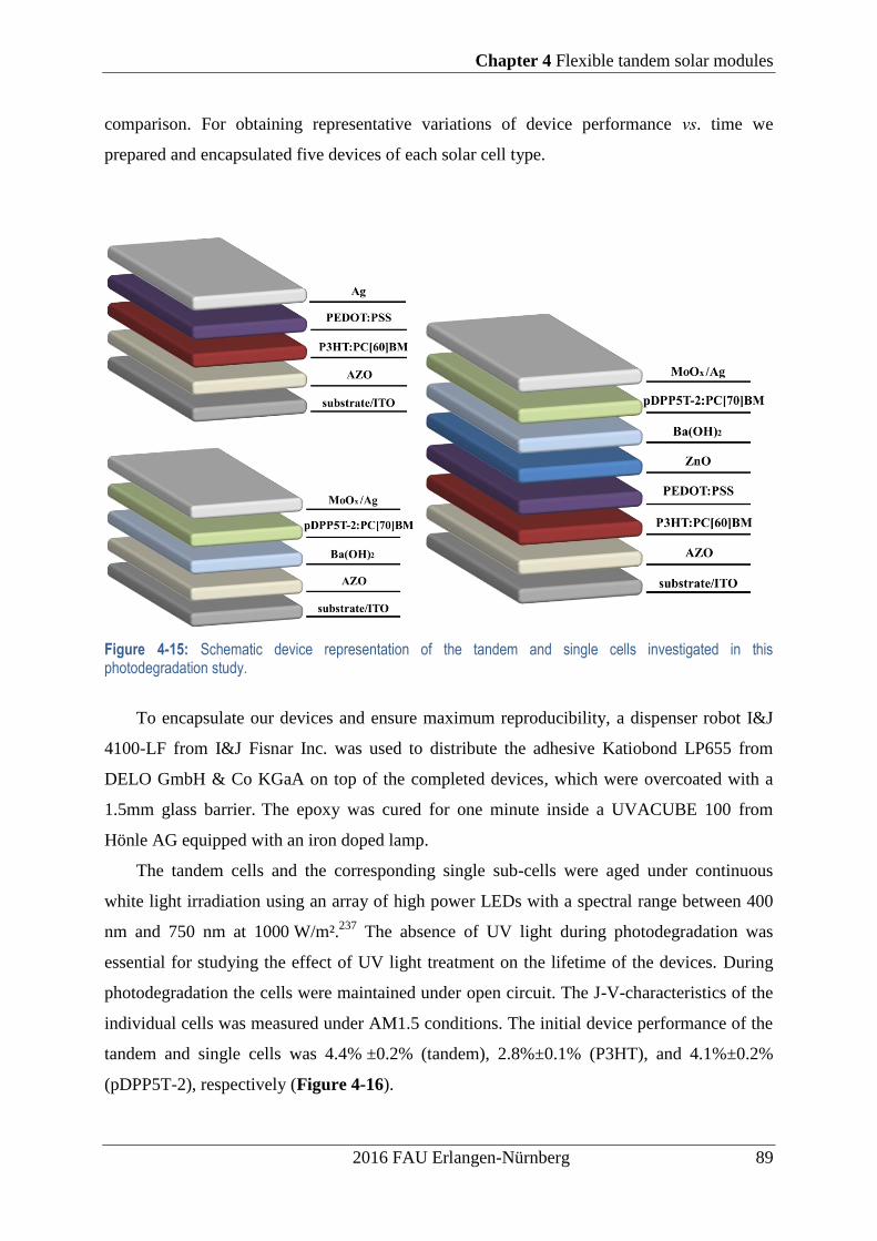
Chapter 4 Flexible tandem solar modules
2016 FAU Erlangen-Nürnberg 89
comparison. For obtaining representative variations of device performance vs. time we
prepared and encapsulated five devices of each solar cell type.
Figure 4-15: Schematic device representation of the tandem and single cells investigated in this photodegradation study.
To encapsulate our devices and ensure maximum reproducibility, a dispenser robot I&J
4100-LF from I&J Fisnar Inc. was used to distribute the adhesive Katiobond LP655 from
DELO GmbH & Co KGaA on top of the completed devices, which were overcoated with a
1.5mm glass barrier. The epoxy was cured for one minute inside a UVACUBE 100 from
Hönle AG equipped with an iron doped lamp.
The tandem cells and the corresponding single sub-cells were aged under continuous
white light irradiation using an array of high power LEDs with a spectral range between 400
nm and 750 nm at 1000 W/m².237
The absence of UV light during photodegradation was
essential for studying the effect of UV light treatment on the lifetime of the devices. During
photodegradation the cells were maintained under open circuit. The J-V-characteristics of the
individual cells was measured under AM1.5 conditions. The initial device performance of the
tandem and single cells was 4.4% ±0.2% (tandem), 2.8%±0.1% (P3HT), and 4.1%±0.2%
(pDPP5T-2), respectively (Figure 4-16).

Chapter 4 Flexible tandem solar modules
90 2016 FAU Erlangen-Nürnberg
Figure 4-16: Initial J-V characteristics of a representative tandem cell and their respective sub-cells
To gain insight into the effect of the UV light-soaking process, we looked into the
transient behavior of the UV treatment. Figure 4-17 shows the periodically measured change
of the photovoltaic parameters upon UV irradiation using the tandem cells. In between J-V
characterization, the cells were stored in the dark at room temperature in order to discard any
impact on the UV light soaking state due to exposure to ambient light. Upon UV light
soaking, the FF increases dramatically (~45%) while Jsc increases by about 5% and Voc barely
changes. It is well documented in the literature that UV radiation can improve the electronic
properties (conductivity) of the ZnO layer as well as the contact at the ZnO interface.269-271
This is most likely the reason for the J-V characteristics translating from a double-diode type
behavior (S-shape) to a diode behavior with high FF. According to Figure 4-17 the light
soaking state remains constant for about 10 h after which the photovoltaic performance
decays sharply. Moreover, Figure 4-17 reveals that the light soaking state features a half-time
of about 200 h and is, therefore, expected to contribute decisively to the burn-in period in
OPVs containing ZnO.

Chapter 4 Flexible tandem solar modules
2016 FAU Erlangen-Nürnberg 91
Figure 4-17: Long-term decay of the UV light soaking (LS) state in the dark. Each data point represents the
average value of 5 tandem cells. The filled symbols represent the condition after immediate light soaking, whereas the hollow symbols represent the temporal decay of the LS state. The data were extracted from J-V-measurements using an AM1.5 spectrum and an illumination power of 1000W/m². Outside the J-V-measurements the tandem cells were stored in the dark at room temperature.
From the previous result we can deduce the importance of UV light exposure during
continuous 1-sun irradiation. We, therefore, designed a long-term aging test, in which the
solar cells were exposed to UV light for 10 s prior to each J-V measurement. Figure 4-18
shows the average long-term temporal evolution of Voc, Jsc, FF, and PCE for the single and
tandem cells under continuous illumination with intermittent UV treatment. The burn-in
period extends to about 1100 h, after which the decay of the PCE follows a close to linear
trend (Figure 4-18d). Remarkably, in the long-term measurements the tandem cells showed
the most stable behavior by losing only 11% of the initial value after 2000 h. The PCE of
P3HT and pDPP5T-2 based single cells followed a similar decay with losses of 16% and
15%, respectively. Overall, the loss in PCE is mainly determined by a loss in FF (5 – 11%)
and a modest decay in Jsc (0 – 8%). Impressively, in the case of the tandem and pDPP5T-2-
based single cells we observe no current losses throughout 2000 h of light exposure. To put
our results into perspective, PCE drops in the range of 10 – 20% for P3HT single cells and
25% for PCDTBT-based single cell devices under 1-sun exposure and within similar periods
of time have been reported in the past.272-274

Chapter 4 Flexible tandem solar modules
92 2016 FAU Erlangen-Nürnberg
Figure 4-18: Photoaging of single and tandem OPV cells. The graph show the average long-term temporal evolution of PCE, Voc, Jsc, and FF for the different single and tandem cells under continuous white light illumination. The photovoltaic parameters were extracted from J-V-measurements using an AM1.5 spectrum at 1000W/m². Before each J-V-measurements the samples were UV treated (365nm, 10 s). Each data point represents the average value of 5 tandem devices, 5 DPP devices, and 5 P3HT devices.
We speculate that the reason for the enhanced long-term stability of our solar cells is
manifold. Specifically, we used an inverted device structure, thereby eliminating reactive
metal interfaces.275
Additionally, we replaced the widely used but moisture sensitive and
reactive PEDOT:PSS with MoOx as the top buffer layer. The benefit of using the chemically
more inert MoOx for better device stability has been shown before.276, 277
Moreover, we chose
to modify the ETL/pDPP5T-2 (ETL: electron transporting layer) interface with a hole
blocking Ba(OH)2 layer in the case of the more stable tandem and pDPP5T-2 single cells. The
Ba(OH)2 layer has been proven to reduce exciton quenching at cathode interfaces and
improve device efficiency in the case of OLEDs and OPVs.263, 268, 278
Based on our findings,
we hypothesize that Ba(OH)2 could also contribute to stabilizing the ETL/pDPP5T-2 interface
by reducing electronic trap formation and oxygen adsorption. A more elaborate study in this
direction is currently underway. Furthermore, periodic UV light soaking during prolonged
operation is expected to desorb oxygen trapped at the surface of ZnO and AZO. This step is
likely to prevent significant conductivity losses of the ETLs ZnO and AZO, contributing to a
larger FF throughout the lifetime measurements. 270, 279
For an estimation of the lifetime of the tandem solar cells, we applied a linear regression
to the slowly, linearly decreasing PCE data points and extended this line up to 80% of the
initial value (Figure 4-19). In doing so, an extrapolated operating lifetime of ≈27 000 h can
be extracted. Considering an average 1500 hours of sunshine per year in central Europe, this

Chapter 4 Flexible tandem solar modules
2016 FAU Erlangen-Nürnberg 93
represents, under the current conditions, a best case lifetime of ≈18 years. We further derived
a more conservative lifetime for our cells by accounting for the error bars of our
measurement, which still resulted in a lifetime of ≈8 years (Figure 4-19). It is important to
note that the presented operating lifetime was extrapolated from cells, which were aged under
open circuit and under indoor conditions using a LED based solar simulator that does not emit
radiation in the 180–400 nm wavelength range. We recognize that the absence of UV light,
which has been shown to accelerate degradation through bond scission and free radical
formation in OPV semiconducting polymers,280
may artificially increase the lifetime of our
cells. Furthermore, for outdoor conditions in the field, there are influences from other sources
such as natural thermal cycling, shading, and humidity cycling, which need to be taken into
account.
Figure 4-19: Extrapolated lifetime of inverted OPV tandem cells. Long-term PCE decay of inverted P3HT:PC[60]BM and pDPP5T-2:PC[70]BM based tandem solar cells. Each data point represents an average value of 5 tandem devices. For estimating the accelerated lifetime, we applied a linear fit of the form y = 0.899x – 3.6x10⁻⁶ to the data points following the burn-in period and extended the fit to where the efficiency drops to 80% of the initial value (red line). For a minimum expectable lifetime of our cells we extrapolated the minimum (maximum) values of the error bars (dashed lines). The lifetimes were calculated considering an average 1500 hours of sunshine per year (central Europe).
Given that we used a glass-on-glass encapsulation architecture and an evaporated top
electrode, the lifetime presented here certainly reflects an upper bound for the lifetime of this
type of organic tandem solar cells. However, if high quality packaging is used, including UV
filters, combined with better interface materials, e.g., towards blue light soaking, similar
lifetimes are perhaps not impossible but need to be documented by thorough outdoor studies.

Chapter 4 Flexible tandem solar modules
94 2016 FAU Erlangen-Nürnberg
4.5 Conclusion
We demonstrated the complete design and fabrication route for realizing flexible organic
tandem modules. Starting from the choice of solution processed buffer layers with the
appropriate solvents and complementary absorption photoactive materials we performed
optical simulations to predict the efficiency and we developed a process recipe that can be
transferred to flexible substrates. Flexible tandem cells with efficiency of 6.1% were
produced. Then, we used a fs-laser as a means for separating and interconnecting the cells.
The laser features high speed and high precision patterning in lateral and in z-directions. As a
result, tandem modules with geometric fill factors beyond 90% and high-quality electrical
interconnects are feasible, leading to minor photovoltaic losses compared to the non-patterned
tandem cells. Considering the low temperatures involved (<70 °C) throughout device
fabrication and possible laser writing speeds, the process is fully roll-to-roll, large scale
compatible. Our champion tandem modules, consisting of three series connected cells, deliver
a power conversion efficiency of 5.7% and a voltage output of 3.9 V. Bending tests manifest
high mechanical resilience, demonstrating that this type of flexible cells could potentially be
implemented as a power source on non-planar, foldable and movable surfaces of textiles,
mechatronics and buildings. Additionally, we proved that our device geometry shows high
stability under continuous white light illumination with PCE loss of only 11% within the first
2000h of operation. By extrapolation we found operating lifetime in excess of one decade.
Even though the presented devices show high applicability and process that can be easily
adapted in a production line, there are some last stairs to climb in order to fully exploit the
potential throughput of solution process technology. That of the solution process electrodes.

2016 FAU Erlangen-Nürnberg 95
Chapter 5 Lamination as fabrication strategy Parts of this chapter have been adapted or reproduced with permission from:
o G. D. Spyropoulos, C. O. Ramirez Quiroz, M. Salvador, Y. Hou, N. Gasparini, P. Schweizer, J. Adams,
P. Kubis, N. Li, E. Spiecker, T. Ameri, H.-J. Egelhaaf and C. J. Brabec, Energy Environ. Sci., 2016,
DOI: 10.1039/C1036EE01555G
5.1 Motivation and State of the art
Thin-film photovoltaics using high throughput solution-based printing techniques such as
roll-to-roll processing is a key technology for inexpensive and sustainable light-to-energy
conversion. However, to fully exploit the economical and engineering advantages with which
the roll-to-roll printing technology could benefit an industrial scenario for thin-film
photovoltaics, fully solution-processable photoactive and electrode materials are required.
Solution-processed metal electrodes are particularly difficult to realize because of often
inferior optical (e.g., reflectivity) and electrical properties (e.g., conductivity) as compared to
the more common vacuum deposited metal electrodes. Moreover, processing a metal based
electrode from solution on top of a semi-finished stack is challenging in terms of solvent
compatibility, surface energy and even surface induced damaging. Nevertheless, important
advances have been demonstrated lately using for instance silver ink167
, silver nanowire154, 155,
161, carbon allotrope
262, 281 and hybrid electrodes, e.g., conductive polymer/metal grids
282, 283,
without significant sacrifices in efficiency.
An alternative concept for realizing high-quality metal electrodes in a low-cost, large-
area compatible fashion is roll lamination. In general, a transparent, conductive film with
adhesion properties (TCA; transparent conducting adhesive) coated on a substrate provides
electrical and mechanical functionality and is activated by applying temperature and/or
pressure. This method is particularly attractive because it allows decoupling the processing of
the top metal electrode from the rest of the device fabrication procedure. This could greatly
simplify a production line, for instance, by allowing switching between the fabrication of
single cells and tandem solar cells, the latter via post-connection of two sub-cells.
Furthermore, the substrate of the laminated top electrode could function as barrier and thus
enable encapsulation at the earliest possible fabrication stage.
Previous work has focused on demonstrating lamination as a potentially simple
fabrication route for bilayer structures284, 285
, organic light-emitting diodes286
, semi-
transparent organic solar cells287
and metal electrodes in general288-290
. In this context, a

Chapter 5 Lamination as fabrication strategy
96 2016 FAU Erlangen-Nürnberg
conductive adhesive consisting of PEDOT:PSS and sorbitol has proven to be particularly
effective, but other conductive glues have been explored as well291-296
. Organic solar cells
produced with this method have shown power conversion efficiencies up to 4% (Table 5-1).
More recently alternative materials and lamination techniques to produce single or tandem
organic and perovskite solar cells were presented96, 297-299
.
Table 5-1: Power conversion efficiencies of laminated organic solar cells due date
Research group PCE (%)
J. Huang et al. 2008287 3.00
B. A. Bailey et al. 2011291 3.19
Y. Yuan et al. 2011292 4.00
C. Shimada et al. 2013293 2.41
D. Kaduwal et al. 2014294 2.50
R. Steim et al. 2015290 1.60
G.D. Spyroppoulos et al. 5.88
While previous results are indicative of the future potential of lamination technology, at
present the implementation of this technology as efficient method for producing up-scalable
electrodes and devices hinges on several hurdles. First, thick electrode materials (micron
range) that efficiently extract charge carriers upon being coated using simplified solution-
based methods are not easily accessible. The main challenges associated with the realization
of such a functional electrode are often limited by the trade-off between the adhesion and the
electrical properties as well as by the quality of the contact between the TCA and the active
layer on one side and the TCA and the current collection electrode on the other side.
Additionally, a proof of concept by transferring this technology to a solar module that
delivers tunable voltage output is needed to demonstrate the feasibility and applicability of the
concept. Importantly, the fabrication of a module using a laminated electrode bears several
key challenges associated with the realization of an efficient electrical connection between
two successive cells (P2 line) and the separation of the top electrode (P3 line) for defining
electric current pathways, in both cases without sacrificing the active area. Specifically, high
performance devices call for a top electrode that fills the P2 area and forms an ohmic contact
with the bottom electrode upon lamination (Figure 5-11, Figure 5-12). Furthermore, a second
important challenge lies in aligning the P3 line relative to the P2 line when laminating the
electrode on top of the active layer (Figure 5-11, Figure 5-12). This may induce major

Chapter 5 Lamination as fabrication strategy
2016 FAU Erlangen-Nürnberg 97
photocurrent losses because standard procedure requires the typically pre-patterned P3 line to
be wide enough so that the electrical separation is not jeopardised upon lamination, which
necessarily translates into a loss of photoactive area (dead area).
In this chapter, we report on a roll lamination process to demonstrate fully solution-
processed, laminated organic solar modules with 5.3% power conversion efficiency. This was
accomplished by developing a highly functional adhesive electrode consisting of embedded
silver nanowires and a transparent conductive adhesive (TCA). The latter is based on a blend
of highly conductive PEDOT:PSS and D-sorbitol. We investigate the optoelectrical quality of
this laminated top electrode using full-frame dark lock-in thermography (DLIT), impedance
spectroscopy (IS) and capacitance versus voltage measurements (C-2
-V). A key innovation of
the flexible modules with laminated top electrode is depth-resolved post-laser patterning using
a pulsed femtosecond laser. The laser beam penetrates the top substrate after the lamination
process and ablates the composite electrode beneath without damaging the top plastic
substrate. This step eliminates common alignment constraints of traditional module coating
and allows for large geometrical fill factors (>90%). We further confirm the general
application of this concept by fabricating laminated perovskite solar cells and modules with
9.80% and 9.75% efficiency, respectively. We thus anticipate that the adhesive
AgNW:PEDOT composite electrode by itself or combined with depth-resolved laser
patterning is likely to be compatible with and of benefit to many thin film photovoltaic
technologies.
5.2 Realization of efficient adhesive top electrode
In order to find and optimize an efficient adhesive top electrode we cycled over
optoelectrical analysis and fabrication. First, we fabricated flexible photovoltaic devices with
laminated top electrode by adopting a solution process that is based on doctor blade coating in
air (Figure 3-4). Once again, we chose an IMI coated PET foil as a transparent bottom
electrode. On top of IMI, we processed commercial ZnO nanoparticles (Nanograde) as
electron selective electrode. As photoactive layer we coated a medium band gap conjugated
polymer PBTZT-stat-BDTT-8165, 300
blended with phenyl-C61-butyric acid methyl ester
([60]PCBM) on top of ZnO (see Chapter 3). The active layer was contacted with a laminated
electrode that was prepared in a separate step.

Chapter 5 Lamination as fabrication strategy
98 2016 FAU Erlangen-Nürnberg
-Challenges
The road towards an efficient adhesive top electrode concealed several challenges
regarding materials and device architecture design. Literature survey showed similarities for
all work presented due that date; a transparent conductive adhesive (TCA) was deposited on
top of a more conductive layer. Initially, we scanned several materials to realize a TCA by
measuring the conductivity of a sandwich structure where two conductive substrates (IMI or
ITO) were connected with a TCA by pressed through a laminator. Combinations such as
acrylic adhesives-highly conductive PEDOT:PSS, acrylic adhesive- metallic NPs/AgNWs,
UV curable adhesive (such adhesives are used for encapsulation of optoelectronics e.g. Dello
Katiobond)- metallic NPs/AgNWs. For the time of our investigation we found-in accordance
to the literature- that a combination of a highly conductive PEDOT:PSS with D-sorbitol gave
the best balance between adhesion and electronic characteristics. On the one hand, when D-
sorbitol is introduced in water based solution- such as PEDOT:PSS- promotes a gel formation
that upon pressing and applied temperature activates strong collective hydrogen bonding. On
the other hand, it has been extensively proven that D-sorbitol and other substances of the
same family (e.g sugar alcohols, EG, PEG) can improve electronic conductivity and promote
ionic conductivity in PEDOT:PSS.293, 301-304
Thus, initially we combined a TCA based on
mixture of PEDOT:PSS and D-sorbitol with IMI substrate to form a top laminated electrode.
Then, to realize an organic solar cell, employing the laminated electrode described in the
previous paragraph, we followed an architecture design similar to the one with evaporated
electrode (Figure 5-1). In such architecture, the total active area of the cell (the overlap of top
and bottom electrode) is defined by the top adhesive electrode. However, following such a
structure, we encountered serious shunting problems over the whole active area. These shunts
were mainly occurring on the sides of the laminated electrodes as we verified with DLIT
imaging (Figure 5-1). To circumvent this problem we laser structured our bottom IMI
electrode to electrically isolate the active area from the edges of the substrate (Figure 5-1).
By doing so we found consistently higher shunt resistance (Rp) values which resulted in
higher FF (~45%) and efficiencies. The substantial mitigation of the shunts was verified by
DLIT imaging, where a more uniform- without bright spots- flow of current reveals the
superiority of the device (Figure 5-1). Even though a critical step towards efficient solar cells
with laminated top electrode, still our devices suffered from high series resistance (Rs). These
resistance losses led to limited FF, Jsc and Voc values. Optimization on TCA thickness,
lamination pressure and temperature could not take us any further on the efficiency roadmap.

Chapter 5 Lamination as fabrication strategy
2016 FAU Erlangen-Nürnberg 99
All these problems were solved with the introduction of AgNWs in our structure, as will be
described in the next section.
Figure 5-1: The effect of patterning in solar cells with laminated top electrode. Left side: realization of laminated solar cell with unpatterned bottom IMI. Right side: the realization of laminated solar cell with laser patterned IMI. Typical J-V characteristics under 1 sun illumination and DLIT images are shown for both architectures.
-Efficient adhesive electrode
In contrast to previous work, where primarily the combination of a transparent
conductive adhesive with sputtered electrodes287
and evaporated294
or complex mesh
structures293, 295
has been explored, the laminated electrode designed in this work consists of a
bilayer of successively coated TCA and AgNWs on PET foil (Figure 3-4b, Figure 5-2). As
TCA we optimized a mixture of highly conductive PEDOT:PSS (~850 S/cm) and D-
Succesive
coating of both
substrates
Lamination
Electrical &
optical
characterization+
-
PET / IMI
ZnO / Act. Layer
TCA
PET / IMI
+
-

Chapter 5 Lamination as fabrication strategy
100 2016 FAU Erlangen-Nürnberg
sorbitol287
. The highly conductive PEDOT:PSS ensures sufficient electrical connection
between the active layer and the AgNWs, while D-sorbitol provides the necessary adhesive
force for establishing a robust connection between the two substrates. Significantly, the
combination of TCA with AgNWs affords process simplicity, semitransparency and high
quality electrical contacts. AgNWs are easily coated from a water-based solution, requiring
only a simple and short drying process at 100 °C for 3 min. Aside from the ease of processing,
AgNWs are known to form macroscopic mesh electrodes (Figure 5-2b) with low sheet
resistance (10 Ω/sq) and average optical transmittance of better than 70% (Figure 5-4).
Notably, we found good ohmic contact with the conductive adhesive, enabling charge carrier
extraction similar to evaporated silver, as discussed later on. Importantly, the AgNWs
electrode is compatible with the technical requirements of many photovoltaic technologies
and can be easily exported to, e.g., CIGS (copper indium gallium selenide solar cells) or a-
Si:H (amorphous silicon) , facilitating the implementation of hybrid tandem technology.
Figure 5-2a depicts a macroscopic cross sectional scanning electron micrograph of a device
with laminated top electrode. It is apparent that the TCA (~2 m) is substantially thicker than
the active layer (280-290 nm). The overall thickness of the TCA is the result of the
combination of optimized coating of the glue, applied pressure and resulting adhesion. We
further note that polymer blend layers featuring PBTZT-stat-BDTT-8 can be coated as thick
as 500 nm without significant roll off in photovoltaic performance300
.
Figure 5-2: Cross-section scanning electron microscopy (SEM) image of flexible laminated organic solar device (left). Top view of AgNWs on TCA after delamination of PET substrate(right).
The J-V characteristics of flexible OPV solar cells with laminated and evaporated
electrode under 1000 W m-2
solar simulator light are shown in Figure 5-3a. The Optimized
solar cells with laminated top electrode deliver an open circuit voltage (Voc) of 810 mV, a

Chapter 5 Lamination as fabrication strategy
2016 FAU Erlangen-Nürnberg 101
short circuit current density (Jsc) of 12.10 mA cm-2
and a fill factor (FF) of ≈59%. This
corresponds to a power conversion efficiency of 5.9%. Comparison between OPV devices
with laminated and evaporated silver electrode (the latter consisting of IMI/ZnO/PBTZT-stat-
BDTT-8:PC60BM/PEDOT:PSS(≈50nm)/Ag, evaporated) reveals that the losses in PCE are
mainly dominated by Jsc losses (≈5%), which is in good agreement with the integrated
photocurrent from corresponding EQE spectra (Figure 5-3b). The difference in Jsc is likely to
be associated with differences in electromagnetic field distribution and resulting interference
profile.
Figure 5-3: a) Current – Voltage (J-V) characteristics of organic solar cells with laminated and evaporated top electrode b) EQE spectra of reference OPV solar cell with evaporated silver top electrode (100 nm, blue dashed line), laminated OPV solar cell with reflecting mirror in the back (black line), laminated OPV solar cell measured without reflecting mirror (green line).
It is intriguing that such a thick polymer/adhesive/AgNW-based laminated electrode as
the one shown in Figure 5-2a allows efficient photovoltaic performance. In the following we
analyze the optical and electrical properties of the laminated composite electrode. Figure 5-4
shows typical transmission spectra of the laminated electrode, the PET substrate and relevant
charge extraction layers. The transmission spectrum of the TCA electrode shows the
characteristic localized surface plasmon resonance of AgNWs around 380 nm and an average
transmission of ≈70% between 400 nm and 800 nm. The final OPV devices with adhesive top
electrode and an active layer of 290 nm show an average transmittance of ≈31% for the same
wavelength range.
a b

Chapter 5 Lamination as fabrication strategy
102 2016 FAU Erlangen-Nürnberg
Figure 5-4: Transmittance spectra of PET substrate, charge extraction layers and laminated electrode
To investigate the electrical characteristics and homogeneity of the laminated
electrode we applied impedance spectroscopy and dark lock-in thermography (DLIT). DLIT
is a sensitive full-frame infrared imaging technique that reveals local thermal loss
processes305
. Figure 5-5a compares two devices with laminated and evaporated top electrode
but with otherwise identical layer stack. For DLIT measurements, the devices were operated
under 1V forward bias (charge carrier injection regime). Both electrodes show a typical
temperature gradient behavior with higher temperatures closer to where the IMI electrode was
contacted (Figure 5-5a,b). This observation originates from the difference in sheet resistance
between the bottom electrode (IMI) and the top electrode of the solar cell (evaporated or
laminated)305, 306
. The laminated electrode reveals a DLIT image with similar temperature
profile gradient and homogeneity than the device with evaporated silver, suggesting a
homogenous and fully functional electrode with no major irregularities in current transport
across the IMI and laminated AgNWs electrode.

Chapter 5 Lamination as fabrication strategy
2016 FAU Erlangen-Nürnberg 103
Figure 5-5: DLIT images of solar cells with evaporated and laminated top electrode and c) integrated DLIT signal profile along the long axis of the DLIT image.
In order to further investigate the effect of the laminated electrode on the device
behavior, we conducted AC impedance spectroscopy and capacitance versus voltage
measurements307-309
. The Nyquist plots in the dark for varied applied bias are represented in
Figure 5-6a,b. Similar to previous reports on OPV devices, the data is best fitted using an
equivalent circuit model that includes two resistor-capacitor sub-circuits and an additional
resistive element due to electrode resistance losses (Figure 5-6c) , which accounts for the
total resistance in the device 307, 308
. Using this model, we extract the resistance elements of
our devices over the range of different applied bias. It has been previously established that the
high-frequency impedance response is primarily related to the transport resistance (Rt) of
photo-generated carriers being extracted at the contacts while the low-frequency response can
be associated with recombination resistances in the bulk (Rrec)307, 308
. Qualitatively, for
optimum device performance Rrec should be large and Rt small for voltages corresponding to
the fourth quadrant of the J-V graph. The recombination resistance of devices with evaporated
electrode is almost identical to the ones with, laminated electrode as demonstrated by the
similar exponential decay with applied bias (Figure 5-7a). Minor variations in the regime V <
Voc may reflect small variations in device thickness or in the electrical field distribution. This
is not surprising considering the usage of the same photoactive blend. For voltages greater
than Voc the recombination resistance approaches zero in both cases, reflecting the higher
probability for the generated carriers to vanish through bimolecular recombination.
Conversely, a comparison between the transport resistance (Rt) shows values of similar order
of magnitude (two orders of magnitude lower than Rrec) but higher over the whole scan of
voltages for the device with a laminated top electrode (Figure 5-7b). The increased Rt is
representative for a higher contact resistance of the laminated electrode and probably further
Evaporated Electrode
Laminated Electrode
a b

Chapter 5 Lamination as fabrication strategy
104 2016 FAU Erlangen-Nürnberg
dominated by the outstanding large thickness of the TCA in the laminated devices. Since the
probability for charge extraction depends on the correlation between Rrec and Rt310
, the
observation of comparatively low Rt, even in the case of laminated devices, grants efficient
carrier extraction in both cases and thus comparable device performance.
Figure 5-6: a) Impedance spectra for devices with evaporated top electrode under different applied biases. b) Impedance spectra for devices with laminated top electrode under different applied biases. EIS Spectrum Analyser was used for analysis and simulation of impedance spectra311. c) Equivalent circuit used for fitting data obtained by impedance spectroscopy. Cg and Cμ represent geometrical and chemical capacitance, respectively.. Rrec denotes the recombination resistance and Rt represents the transport resistance. Rs´ denotes an additional resistive element due to electrode resistance losses.. For applied biases greater than Voc the total series resistance in the model is given by Rs = Rs´ + Rt
Figure 5-7: a) Recombination resistance Rrec and b)transport resistance Rt as a function of applied bias for devices with evaporated and laminated electrode.
a b
c
a b

Chapter 5 Lamination as fabrication strategy
2016 FAU Erlangen-Nürnberg 105
Mott-Schottky (C-V) measurements can reveal important insight regarding the quality
of the electrode and electrode-bulk interface309
(Figure 5-8), particularly when comparing
laminated and evaporated electrodes. By fitting a straight line to the region of C-2
vs. V with
the steepest slope it is possible to extract the built-in potential (Vbi)309
. Importantly, both
devices demonstrate similar values of Vbi (~0.57 V), which evidences qualitatively similar
energetic offsets at the electrode-bulk interface. In addition, in the high reverse bias regime
(V<<Vbi) both samples show dielectric capacitor behavior, approaching a constant capacitance
that corresponds to the geometrical capacitance309
. In the forward bias regime (V > Vbi), the
capacitance is mainly determined by the chemical capacitance309
. Different Mott-Schottky
behavior under low reverse and forward bias (V < Vbi) is observed. For devices with
evaporated electrode the capacitance starts increasing at more negative voltages, denoting an
early starting point of a more gradual decrease of the depletion width and high doping density
N=1.04 × 10¹⁶
cm-3
. The latter is determined from the corresponding slopes by N= - 2(dC(x)-
2/dV)
-1 / qε0εrA
2, where q denotes elementary charge, ε0 dielectric constant of vacuum and εr=
dielectric constant of the semiconductor (assumed value of 3.5)312
. In contrast, laminated
devices show an inclination point at relatively lower reverse (more positive) bias, revealing a
faster depletion zone collapse over the voltage scan and a lower doping density N=5.09 × 10¹⁵
cm-3
. The higher doping density for devices with evaporated electrode may arise due to the
diffusion of small molecules such as oxygen and water migration or evaporated “hot” silver
atoms into the photoactive layer313-315
. These phenomena have been reported before and in the
case of oxygen and water could be even propelled due to intimate contact of the active layer
with a wet, water based PEDOT:PSS solution during device fabrication. For laminated
electrode devices, the TCA was coated on a different substrate and applied on top of the
active layer after a drying step. The difference in doping density highlights the possible
advantage of a procedure, in which electrodes or additional layers are processed on different
substrates and assembled afterwards.

Chapter 5 Lamination as fabrication strategy
106 2016 FAU Erlangen-Nürnberg
Figure 5-8: Mott-Schottky plot (10Hz) for devices with evaporated and laminated top electrode. The dashed lines represent linear fits to the slope. A scheme of the equivalent electrical circuit model used for analyzing impedance spectroscopy data is displayed in Figure 5-6.
In order to characterize the performance of our devices as a function of mechanical stress,
we performed bending tests on a drum with 28 mm radius (Figure 5-9). We reinforced the
edges of the devices using a commercial adhesive tape (ScotchTM
tape). After 1000 bending
cycles the performance decreases to ~59% of initial value mainly due to Jsc and FF losses.
This suggests that the main cause for mechanically induced performance roll off is damages
imposed to the interface between active layer and adhesive electrode.
Figure 5-9: Normalized device characteristics of a flexible organic laminated solar cell over successive bending cycles.

Chapter 5 Lamination as fabrication strategy
2016 FAU Erlangen-Nürnberg 107
The above-mentioned properties grant tremendous inherent advantages to the laminated
electrode: low temperature (≤120°C), minimized contamination (solutions printed on different
substrates ensure reduced contamination of the active layer) and vacuum free (easy, fast and
inexpensive lamination) processing are the most important attributes leading to a high quality
semi-transparent electrode with the additional benefit of simultaneously acting as a protective
barrier towards the environment.
5.3 Innovating solution-processed solar modules
Our proposed fabrication route for realizing solar modules with laminated top electrode
involves an innovative depth-resolved post-patterning technique (Figure 5-10). The
fabrication is fully roll-to-roll compatible due to the high processing speed of our laser
patterning approach (up to 4 m s-1
) and solution processing of all functional layers under
ambient conditions. The device fabrication consists of seven consecutive coating, lamination
and patterning steps. Generally, in order to achieve electrical series interconnection between
individual cells in a solar module, three patterning lines P1 – P3 are necessary (Figure 5-11,
Figure 5-12). We utilize femtosecond–laser patterning with optimized ablation thresholds
(Figure 3-7) for each interconnection line to take advantage of high spatial resolution and low
geometrical fill factor (GFF, ratio between the photoactive area and the total area of the
module) losses.
The advantages and challenges associated with laser patterning of thin-film solar modules
have been elucidated before 316
. Typically, a laser source irradiates the active layer material of
a device with ultra-short laser pulses, inducing a phase transition from solid to vapor. The
minimum energy required for this phase transition is an intrinsic material property and known
as the ablation threshold. Given the differences in the ablation threshold for the electrode,
interface and photoactive materials chosen here (reported in Figure 3-7) and by tuning the
laser fluence, we can ablate functional layers of a device individually. Crucially, we
demonstrate that controlled ablation of functional layers is even feasible through a plastic
barrier, i.e., upon lamination of the top electrode, extending the concept of laser patterning to
depth-resolved laser patterning. This allows effectuating the last patterning step upon
protecting the susceptible device structure from environmental contaminants.

Chapter 5 Lamination as fabrication strategy
108 2016 FAU Erlangen-Nürnberg
Figure 5-10: Step-wise fabrication route of solution-processed roll laminated modules.
Figure 5-11: Architecture of laminated organic solar cell/module and illustration of depth-resolved post patterning of the top electrode (P3) using a femtosecond laser. Inset shows laser-patterned lines required for interconnection of successive cells, i.e. module fabrication.
PET
Ag NWs
TCA
PBTZT-stat-BDTT-8:PCBM
ZnO
PET/IMI
Depth-Resolved Post Patterning
P3 P2 P1

Chapter 5 Lamination as fabrication strategy
2016 FAU Erlangen-Nürnberg 109
Figure 5-12: The P1 and P2 line are scribed before the lamination process while the P3 line is post-patterned through the top substrate.
We now turn to the laser patterning steps for module fabrication based on laminated
devices. Figure 5-13 illustrates the top view of fabrication route revealing also the module
layout of our devices. Following our experience from single solar cells we laser structure the
bottom IMI electrode for electrically isolating the edges of the substrate, in an opposite case
we would face dramatic losses form shunting as described in sub-chapter 5.2 , and define the
sub-cells of the module (P1 line) (Figure 5-13). The electron extraction ZnO layer and
photoactive layer are successively coated. During the third step of the module fabrication the
active and ZnO layers are ablated to form the P2 line (Figure 5-13).
Figure 5-13: Top view illustration of the module layout and the preparation road. .
This requires a laser fluence smaller than the ablation threshold of the bottom electrode
(Figure 3-7). It is critically important that the P2 line is free of residuals and debris as this is
the area that will later determine the quality of the electrical interconnection (between top and
successive bottom electrode). In a separate process, the TCA and AgNWs are consecutively
coated on a different substrate to form the top electrode, which is simply assembled on top of
dead area
P1 P2 P3
Substrate
ITO/IMI
ETL
Active Layer
TCA
AgNWs
Substrate
P1 laser
patterning
Coating &
P2 laser patterningLamination &
P3 laser patterningCharacterization

Chapter 5 Lamination as fabrication strategy
110 2016 FAU Erlangen-Nürnberg
the active layer by passing through a pre-heated (120 °C) roll-laminator (pressure ~2 bar,
Figure 3-4c). The final patterning of the top electrode is then performed through the plastic
substrate using depth-resolved laser structuring. We emphasize that the laser fluence can be
fine tuned such that the TCA/AgNWs electrode is selectively ablated -without notably
damaging neither the top PET substrate nor the bottom electrode. The depth selectivity of this
process is demonstrated by plotting the ablation depth as a function of the laser fluence
(Figure 5-14a, left) as well as the corresponding depth profiles (Figure 5-14a, right). The
latter was extracted from confocal microscopy images upon laser structuring of the
TCA/AgNWs layer (Figure 5-14b). We observe that after a relatively slow increase of the
ablation depth with increasing laser fluence the depth increases rapidly after ~2.5 J/cm2. We
associate the slow initial increase with the melting and consecutive ablation of the top
AgNWs film while the steeper slope is likely related to the removal of the TCA. A ~2 m
thick TCA layer can be fully ablated at a laser fluence of ~3 J/cm2. While this laser fluence
exceeds the threshold fluence for the bottom IMI (Figure 3-7) the 2 m thick TCA acts as a
buffer layer and protects the rest of the device from potential damage. Figure 5-14b
visualizes the topography of a representative P3 line as obtained with a confocal microscope
after delaminating the top PET substrate. We note that even though throughout the ablation of
the TCA the laser beam may penetrate and thus dissipate part of the photovoltaic blend layer
this does not affect device performance as the ablation occurs within the dead area, which
does not contribute to the photocurrent of the device. Instead, the main concern for the dead
area when scribing the P3 line is to preserve the electrical pathway by not destroying the
bottom electrode.
Based on the above results, it is clear that the combination of lamination and depth-
resolved laser patterning is particularly attractive because it alleviates both typical constraints
in fabricating thin-film devices from solution as well as active area losses. Furthermore, the
top substrate may simultaneously act as a barrier. In a large-scale fabrication line this
procedure would allow environmental protection of the sensitive active layer at an early
fabrication stage. Simultaneously, this method reduces fabrication complexity as the
adjustment of the P3 line with respect to the P2 and P1 lines can be well controlled with the
laser and obviates mechanical alignment of the substrates. Importantly, the introduction of
depth selective laser scribing constitutes the first step towards a post-patterning technology in
which all patterning lines (P1, P2 and P3) can be scribed by depth-resolved laser patterning.
The later would be applied as the very last device fabrication step upon uniform full-area

Chapter 5 Lamination as fabrication strategy
2016 FAU Erlangen-Nürnberg 111
Figure 5-14: a) (Left) Ablation depth upon laser patterning of adhesive top electrode versus the laser fluence applied. (Right) Representative ablation depth profiles for different laser fluences as determined from confocal optical microscopy images. b) Schematic representation of post-laser ablation of a P3 line through a PET foil after lamination and corresponding 3D depth profile.
coating of all functional layers. Finally, integration of such a fabrication route in a future solar
factory would allow not only for a continuous production line of inexpensive, semi-
transparent and flexible solar modules but also, more generally, for post-connection of two
parallel production lines into a tandem or multilayer concept.
0 100 200 300 µm
µm
0
50
100
150
200
250
300
µm
0
1
2
3
4
5
6
0 100 200 300 µm
µm
0
50
100
150
200
250
300
µm
0
1
2
3
4
5
6
PET
TCA/AgNWs
a
b

Chapter 5 Lamination as fabrication strategy
112 2016 FAU Erlangen-Nürnberg
Remarkably, we demonstrate OPV modules (two in series connected solar cells) with
laminated top electrode that exhibit a champion efficiency of 5.3% and thus only minor losses
in PCE (≈10%) as compared to reference solar cells (Figure 5-15a). These losses are
predominantly determined by the Jsc value, which is only ≈10% lower than the maximum
limit for in series connected modules (current corresponding to half of the reference cell), and
can be attributed to the GFF. The GFF was found to be ~91 % (considering the sum of active
and dead area and neglecting possible bus bar losses)317
. The Voc losses are restrained to ~3%
with respect to the maximum Voc of a two cell module. With 62% the FF is even slightly
higher than in the reference cell, confirming the quality of the active layer and interfaces in
the module. The reported mean values and standard deviation population values of the
laminated devices confirm good reproducibility (Table 5-2). The J-V characteristics in the
dark are shown in Figure 5-15b.
Figure 5-15: a) Current – Voltage (J-V) characteristics of organic solar cells and modules with laminated top electrode. b) J-V characteristics under dark conditions for flexible OPV devices with laminated and evaporated top electrode.
a
b

Chapter 5 Lamination as fabrication strategy
2016 FAU Erlangen-Nürnberg 113
Table 5-2: Key metrics for organic and perovskites solar devices with evaporated and laminated top electrode under AM 1.5G illumination (100 mW cm−2). Best performance and mean values with standard deviation population (shown in parenthesis) were extracted from 10 organic devices and 5 perovskite devices.
Top Electrode V
oc (V) J
sc (mA/cm
2) FF (%) PCE (%)
Device area
(mm2)
PBTZT-stat-BDTT-8: PCBM cell
Evaporated Ag
0.81 (0.80±0.01)
12.70 (12.40±0.18)
60.05 (59.10±0.84)
6.19 (5.87±0.18)
15
PBTZT-stat-BDTT-8: PCBM cell
Laminated
0.81
(0.81± 0.01)
12.10
(11.78±0.28)
59.24
(59.16±0.57)
5.88 (5.65±0.13)
15
PBTZT-stat-BDTT-8: PCBM module
Laminated
1.57 (1.57± 0.01)
5.42 (5.38 ±0.06)
62.31
(60.56±1.28)
5.33 (5.15±0.15)
30
CH3NH
3PbI
3 cell Evaporated Ag
1.04 (1.06±0.02)
18.53 (18.05±0.38)
70.35 (68.09±1.72)
13.56 (13.10±0.32)
15
CH3NH
3PbI
3 cell Laminated
1.01 (1.03±0.02)
16.44 (16.05±0.56)
59.54 (56.61±1.95)
9.80 (9.36±0.40)
15
CH3NH
3PbI
3 module Laminated
2.00 (2.00±0.01)
8.12 (7.90±0.22)
60.00 (57.54±1.60)
9.75 (9.10±0.34)
30
To demonstrate the universality of the proposed method we fabricated perovskite solar
modules with a laminated top electrode featuring the device geometry
ITO/NiO/CH3NH3PbI3/[60]PCBM/ZnO/PEI/Laminated-top-electrode. Methylammonium-
halide based perovskite semiconductors are a particularly challenging example as their
intrinsic sensitivity towards water prohibits top coating of water based solutions. The
photoactive perovskite layer was based on methylammonium lead iodide (see 3.2.4 for
details). A thin film of commercial NiO nanoparticles (Nanograde) was employed as hole
transporting layer while a thin film of ZnO nanoparticles acted as electron-selective interfacial
layer (Figure 5-16a,b). The low-temperature processed NiO nanoparticles were prepared by
flame spray synthesis (see Chapter 3). This process produces crystalline nanoparticles with a
size distribution at the range of 5-8 nm, as determined by transmission electron microscopy
(see Chapter 3). This device architecture was primarily selected because hole and electron
transporting layers along with the intermediate buffer layers can be processed at relatively low
temperatures (140 °C). Moreover, this device geometry has been shown to effectively

Chapter 5 Lamination as fabrication strategy
114 2016 FAU Erlangen-Nürnberg
suppress hysteresis318, 319
. During this work, we observed that ≈10 nm of PEI on top of ZnO
improved the electrical contact with the TCA. A Cross-section SEM image in Figure 5-16b
shows well-defined layers and a TCA of ≈3μm.
Figure 5-16: a) Device architecture of laminated perovskite solar cell/module. b) Cross-section scanning electron microscopy image of laminated perovskite solar device on glass substrate.
The J-V performance of perovskite solar cells with evaporated
(ITO/NiO/CH3NH3PbI3/[60]PCBM/ZnO/PEI/Ag, evap) and laminated contact as well as the
a
b

Chapter 5 Lamination as fabrication strategy
2016 FAU Erlangen-Nürnberg 115
corresponding perovskite module is presented in Figure 5-17a. Reference solar cells with a
thermally evaporated silver electrode demonstrate an average efficiency of 13.56%. When
transitioning to a laminated electrode the average efficiency is reduced mainly due to losses in
Jsc and FF, while Voc remains almost unchanged (Table 5-2). The 11% loss in Jsc is in
agreement with previous reports and can be attributed to optical interference effects as is
apparent from the EQE spectra for wavelengths >550 nm.155, 320
Additional losses could
potentially derive from enhanced transport resistance at the TCA interface as noticed in the
case of laminated OPV devices (Figure 5-7b). This interface is most likely not fully
optimized, even upon improvements after adding PEI on top of ZnO.
Figure 5-17: a) J-V characteristics of perovskite solar cells and modules with laminated top electrode. b) J-V
characteristics under dark conditions for perovskite devices with laminated and evaporated top electrode. c) EQE spectra of reference perovskite solar cell with 100 nm evaporated Ag top electrode (blue dashed line), laminated perovskite solar cell measured with reflecting mirror in the back (black line), laminated OPV cell measured without reflecting mirror (green line).
Perovskite modules show minor losses in efficiency (<1%) as compared to the
corresponding laminated solar cells and deliver a PCE of 9.75%. These losses are governed
by Jsc losses while we observe a full Voc (double Voc with respect to the reference device) and
a
c
b

Chapter 5 Lamination as fabrication strategy
116 2016 FAU Erlangen-Nürnberg
similar FF values. The mean values and the standard deviation of population for all perovskite
devices are shown in Table 5-2. The J-V characteristics in the dark are shown in Figure
5-17b. Importantly, roll lamination of the top electrode initially developed for organic solar
cells and modules can be easily adapted to work with other thin-film photovoltaic
technologies, requiring only an adjustment of the laser fluence for the ablation of the P2 line.
This opens up an entirely new avenue for a cost effective fabrication route of organic and
hybrid electronic appliances.
5.4 Innovating tandem solar cells
As outlined in the previous chapter the tandem concept is a promising approach to
overcome absorption spectrum limitations and thermalization losses, however it presents
several challenges when comes to actual realization. The monolithic development of hetero-
tandem solar cell requires careful planning of active materials, solvent systems, and electrode
materials which they additionally have compatible fabrication methods (e.g. some materials
cannot survive increased temperatures, instead others require temperature annealing). On top
of that, solar cells based on different technologies that follow fundamentally different
production routes with incompatible processes and/or materials are hard if not impossible to
combine. These facts create many times unsolvable puzzles for scientists and engineers. Yet,
the lamination process is a promising fabrication technique to mitigate all these problems and
bring novel solutions.
On this section we present for first time a proof of concept by post-assembling through
lamination process two individually made solar cells in series connection with an
interconnection layer based on solution-processed materials that can be applied in every
photovoltaic technology. The advantages of our concept are tremendous and open new doors
for creation of hybrid technologies tandem devices that is only limited by the imagination of
scientists and engineers.
Our proposed generic fabrication route for realizing laminated tandem solar cell is shown
in Figure 5-18 and is separated to two parallel routes for each sub cell. We utilized our
composite adhesive electrode (PEDOT:PSS:D-Sorbitor/AgNWs) to form the heart of an
efficient adhesive interconnection layer and post-connect in series the two sub-cells.
To prove the generality of our concept we designed and fabricated a hybrid laminated
tandem solar cell based on organic and perovskite sub-cells. The production lines of these
solar cells are diametrically opposed with non-compatible solvents, which constitutes

Chapter 5 Lamination as fabrication strategy
2016 FAU Erlangen-Nürnberg 117
monolithic development very difficult. To form the organic sub-cell (Solar Cell 1, Figure
5-18), we successively coated on IMI substrate to end up with the following geometry;
IMI/ZnO/PBTZT-stat-BDTT-8:[60]PCBM/ PEDOT:PSS / AgNWs/ TCA//. In parallel, a
perovskite sub-cell (Solar Cell 2, Figure 5-18) was constructed with
ITO/PEDOT:PSS/CH3NH3PbI3/[60]PCBM/ZnO/PEI// structure.
Figure 5-18: Step-wise generic fabrication route of laminated tandem solar cell. ETL (bright yellow), Active layers (bright blue, red), HTL (dark blue), AgNWs (yellow grey), TCA (purple).
Finally, after annealing (120 C/10’) of the organic sub-cell, the two sub cells were laminated
together (pressure ~2bar) to form a hybrid laminated tandem solar cell. The architecture of
the resulting laminated tandem solar cell is illustrated in Figure 5-19.
Solar Cell 1
1. Substrate (I) coated
with transparent
electrode
2. Succesive coating of
ETL/Active
Layer(I)/HTL
1. Substrate (II) coated
with transparent
electrode
2. Succesive coating of
HTL/Active
Layer(II)/ETL
Solar Cell 2
Lamination of
Solar Cell 1 // Solar Cell 2
Tandem Solar Cell
3. Succesive coating of
adhesive intermediate layer
AgNWs/TCA

Chapter 5 Lamination as fabrication strategy
118 2016 FAU Erlangen-Nürnberg
Figure 5-19: Architecture of laminated hybrid tandem solar cell.
Figure 5-20 shows the J-V characteristics of the hybrid laminated tandem solar cell and
the corresponding sub-cells under 1000 Wm-2
solar simulator light and in the dark. The
laminated tandem cells demonstrate a Voc of 1.65 V, a short circuit current density of 10.38
mA/cm² and FF of 68%. This corresponds to a power conversion efficiency of 11.65%. and.
Voc values show no losses from the complete summary of the Voc values derived from the
two sub-cells which gives a first indication about the high quality of the adhesive
interconnection layer. The Jsc of the tandem cell is attributed to the efficient current matching
between the current delivered by the two sub-cells and shows relatively low values because of
the strong overlapping of their corresponding EQE spectra (Figure 5-3b, Figure 5-17c).
Higher Jsc values can be obtained in the future with more complimentary materials that cover
a broader spectrum. The unprecedented FF values additionally highlight the quality of our
adhesive intermediate layer. All key metrics with mean values and standard deviation
population values confirm good reproducibility (Table 5-3).
PBTZT-stat-BDTT-8:PCBM
PET/IMI
ZnO
PEDOT:PSS
AgNWs/TCA
ZnO/PEI
PCBM
CH3NH3PbI3
Glass/ITO
PEDOT:PSS

Chapter 5 Lamination as fabrication strategy
2016 FAU Erlangen-Nürnberg 119
Figure 5-20: a) Current – Voltage (J-V) characteristics of hybrid laminated tandem solar cell and the corresponding single cells with laminated top electrode. b) J-V characteristics under dark conditions for the same devices.
Table 5-3: Key metrics for hybrid laminated tandem solar cell and the corresponding single cells with laminated top electrode under AM 1.5G illumination (100 mW cm−2). Best performance and mean values with standard deviation population (shown in parenthesis) were extracted from 5 devices.
V
oc (V) J
sc (mA/cm
2) FF (%) PCE (%)
Laminated Tandem PBTZT-stat-BDTT-8: PCBM/ CH
3NH
3PbI
3
1.65 (1.64±0.01)
10.38 (10.30±0.20)
67.97 (66.70±1.04)
11.65 (11.43±0.20)
Laminated OPV PBTZT-stat-BDTT-8: PCBM
0.80
(0.80± 0.01)
10.52
(10.25±0.25)
59.64
(59.16±0.57)
5.02 (5.00±0.15)
Laminated Perovskite CH
3NH
3PbI
3
0.85 (0.84±0.02)
17.52 (16.97±0.51)
68.74 (67.03±1.60)
10.24 (10.01±0.35)
5.5 Conclusion
The widespread technological adoption of organic and hybrid electronics hinges on the
availability of suitable materials combined with cost-effective fabrication methods for large
area deployment. The material approaches and device engineering methods based on roll
lamination presented here address both of these concerns. A composite electrode based on
ubiquitous PEDOT:PSS and D-sorbitol is combined with Ag NWs to form a highly functional
conductive adhesive that can be coated on plastic substrates. This enables a mechanically
bendable, potentially ultra-low cost electrode with micrometer thickness that could be printed
on a roll-to-roll coater and combined with various technologies, including semi-transparent
a b

Chapter 5 Lamination as fabrication strategy
120 2016 FAU Erlangen-Nürnberg
devices. The composite electrode exhibits transport and recombination resistances comparable
with evaporated silver. A key technological advancement in the fabrication of thin film
modules is attained through the demonstration of depth-resolved, layer selective laser
patterning through the laminated device, which simultaneously grants high geometrical fill
factors, a simplified fabrication protocol and a route towards inherent packaging at the earliest
possible state. As a result, we demonstrated organic and perovskite solar cells and modules
without major sacrifices in efficiency. We further extended this lamination technology to
realize a universal fabrication process based on post connection in series of multilayer
devices. By these means we proved that our composite electrode can also form a high quality
interconnection adhesive layer.
We are confident that this concept will be of relevance to other technologies such as
CIGS, a-Si:H, CZTS ( copper zinc tin sulfide) or HIT (heterostructure with intrinsic thin
layer) solar cells facilitating the production line and providing numerous possibilities for
novel architectures in thin film electronics. We further anticipate that the implementation of
high speed, high precision laser post-lamination patterning enhanced with 3D scribing
capability will further advance the production lines.

2016 FAU Erlangen-Nürnberg 121
Chapter 6 Summary and Outlook
6.1 Summary
A core aspect of my thesis studies envisioned the development of materials and device
fabrication strategies for solution processed solar cells that could be easily translated from the
lab scale to large area, roll-to-roll, compatible processes without sacrificing power conversion
efficiency, stability and conformability. I studied the physics of materials casted from solution
to make high quality, stable thin films with specific functionality inside solar cell architecture;
that includes research on hole/electron transport layers, photoactive layers and electrodes. I
investigated smart processing techniques to fend off the fabrication route of solar cells from
slow and vacuum deposition methods. I combined materials and fabrication methods with
novel laser patterning techniques to demonstrate up-scalable prototypes that would exceed the
scientific experimental boundaries and add applicable values to my research. The
aforementioned can be clearly reviewed on my main projects, in which I, together with fellow
colleagues,: i) demonstrated highly efficient, flexible, solution-processed organic tandem
solar modules adopting roll-to-roll compatible processing (Energy Environmental Science,
first author) and ii) proved the long operating lifetime of the tandem structure (Energy
Environmental Science, shared first authorship), iii) designed an adhesive PEDOT:PSS-Ag
nanowire composite electrode and innovate solution-processing fabrication route for efficient
organic and perovskite solar modules via depth-selective laser patterning of this adhesive top
electrode (Energy Environmental Science, first author, PCT application), iv) innovated multi-
junction devices by post-assembling through lamination process two individually made solar
cells in series connection (manuscript under preparation, PCT appliacation). My findings
inform concrete steps towards efficient, stable and conformable photovoltaics.
6.2 Outlook
-Adhesive electrode
The composite electrode presented in this thesis led to high efficient single-junction and
multi-junction devices. However several improvements can bring the concept of adhesive
electrodes even to higher standards. As I described in Chapter 5 an efficient adhesive
electrode essentially requires two main characteristics; adhesion and conductivity. In an ideal

Chapter 6 Summary and Outlook
122 2016 FAU Erlangen-Nürnberg
case for solar cells, the adhesion medium will also protect the sensitive part of the device from
the ambient. Thus, an ideal TCA will include a UV-curable epoxy usually used for device
packaging. Nevertheless, epoxies are insulators and a medium that gives conductive
properties should be added. Metallic NPs dispersed over the epoxy matrix and form vertical
conduction pathways could be a possible option. Alongside, interesting characteristics such as
anisotropic conductivity can be promoted.
Another aspect that has space for improvement in adhesive electrodes is transparency. In
our proposed adhesive electrode reduction of TCA and AgNWs thickness certainly had an
impact on transparency, but as was noticed in sub chapter 2.4 HC PEDOT:PSS yields to
much lower σDC,B/ σop ratio (FOM for transparent electrodes) than AgNWs. As a result, the
total transmittance of our adhesive electrode is limited by HC PEDOT:PSS, an important
feature when it comes to multi-junction devices. Ideally, since AgNWs demonstrate the
highest σDC,B/ σop ratio for solution processable transparent electrodes, a solution that
combines AgNWs and adhesive properties should be engineered. For the time I invest on this
study, dilution of D-sorbitol in AgNWs water solution and introduction of AgNWs inside an
epoxy matrix did not lead to desirable results.
-Laser patterning
We hypothesize that our depth resolved laser patterning can be extended in the future,
resulting in a complete post-fabrication depth resolved laser patterning for all P1, P2 and P3
lines required for a solar module. In the proposed web design I have added the laser patterning
steps in the end of the process highlighting the potential outcome of this hypothesis. That
would be complete freedom of structuring the final product in the desired form.
Every coating step shown in the proposed web design can be solution process coating
step compatible to roll-to-roll processes (such as; slot die coating, spray coating, inkjet
coating tampo-printing, flexoprinting e.t.c) or even a vacuum deposition method. Drying can
occur with heating units (such as; hot air ovens, infra-red ovens e.t.c). The realization of a
complete post-fabrication depth resolve laser pattering for all required patterning lines of a
solar module is a complicated research problem that would need further investigation and
possibly more advanced laser optics. Alternatively, laser patterning steps can be added in Line
1 and Line 2.

Chapter 6 Summary and Outlook
2016 FAU Erlangen-Nürnberg 123
Figure 6-1: Proposed route for post-fabrication laser patterning of single junction solar device with laminated top electrode.
In Figure 6-1 we proposed a possible route to post-fabrication laser pattern single
junction solar devices with laminated top electrode. In detail, P1 and P3 lines can be patterned
in a similar manner to our proposed depth-resolved laser patterning (sub-chapter 5.3 ). The
contact between two successive cells could be obtained by coating on top substrate a material
that would melt in different laser energy and diffuse through the whole stuck to ensure
electrical connection.
-Tandems
Our laminated tandem solar cells, comprising organic and perovskite sub-cells, clearly
demonstrate the advantages of our novel fabrication route. Employing sensitive active layers
we proved that our materials and processing can be applied to several technologies. In the
boundaries of this thesis we investigated the connection of organics and perovskite solar cells,
however investigation on realizing hybrid tandems by connecting different technologies (such
as CIGS, a-Si:H, CZTS, perovskites and organics) continue.
-Roll-to-roll processing
To help the reader visualize the potential outcome of this thesis, I illustrate in Figure 6-2
a proposed, simplified roll-to-roll set-up that post-connects two parallel production lines (Line
1, Line 2) in a Combined Line. The two lines may produce different solar cells that can be
post-assembled in a tandem concept or solar cell and adhesive top electrode to form a single
junction device. In detail, in Line 1 a first substrate unrolls to meet successively coating and
drying steps (only one pair is shown) that will form all the functional layers. In parallel, and in
Substrate
Bottom Electrode
ETL
Active Layer
TCA
AgNWs
Substrate
Melting contact
Substrate
Bottom Electrode
ETL
Active Layer
TCA
AgNWs
Substrate
pP1
Melting contact
P3

Chapter 6 Summary and Outlook
124 2016 FAU Erlangen-Nürnberg
similar manner, in Line 2 a second substrate undergoes coating and drying steps which may
completely vary from the one followed in Line 1. The two substrates are post-connected in a
Combined Line through a lamination process and additional drying processes may be applied.
Figure 6-2: Laminated roll-to-roll web design with post laser patterning.
The novel architectures and smart device fabrication strategies presented in this thesis
extended the knowledge on the main aspects of every photovoltaic technology; efficiency,
cost and stability. I proved every concept with demonstrators that hold great promises to be
transferred in roll-to-roll production lines of the future market.
Line 1
Line 2
LaminationCoating Drying Drying
CoatingDrying
Combined Line
Laser Patterning

2016 FAU Erlangen-Nürnberg 125
Bibliography 1.
http://www.worldenergyoutlook.org/resources/energydevelopment/energyacces
sdatabase/.
2.
http://www.iea.org/publications/freepublications/publication/Solar_Energy_Per
spectives2011.pdf.
3. http://www.ez2c.de/ml/solar_land_area/.
4. https://en.wikipedia.org/wiki/Solar_energy.
5. A. E. Becquerel, Comptes Rendus de L´Academie des Sciences, 1839, 9.
6. A. E. Becquerel, Annalen der Physick und Chemie, 1841, 54.
7. W. G. Adams and R. E. Day, Proceedings of the Royal Society, London, 1877, A25.
8. C. E. Fritts, American J. of Science, 1883, 26.
9. L. O. Grondahl, Review of Modern Physics, 1933, 5.
10. L. Bergmann, Physikalische Zeitschrift, 1931, 32.
11. F. C. Nix and A. W. Treptwo, Journal Opt. Society of America, 1939, 29.
12. W. G. Adams and R. E. Day, Philosophical Transactions of the Royal Society of London, 1877, 167, 313-349.
13. D. M. Chapin, C. S. Fuller and G. L. Pearson, J. Appl. Phys., 1954, 25, 676-677.
14. http://www.nrel.gov/ncpv/images/efficiency_chart.jpg.
15. J. Gong, S. B. Darling and F. You, Energy Environ. Sci., 2015, 8, 1953-1968.
16. A. C. Arias, J. D. MacKenzie, I. McCulloch, J. Rivnay and A. Salleo, Chemical Reviews, 2010, 110, 3-24.
17. M. Kaltenbrunner, M. S. White, E. D. Głowacki, T. Sekitani, T. Someya, N. S.
Sariciftci and S. Bauer, Nat Commun, 2012, 3, 770.
18. M. Kaltenbrunner, G. Adam, E. D. Glowacki, M. Drack, R. Schwodiauer, L. Leonat,
D. H. Apaydin, H. Groiss, M. C. Scharber, M. S. White, N. S. Sariciftci and S. Bauer,
Nat. Mater., 2015, 14, 1032-1039.
19. M. A. Green, K. Emery, Y. Hishikawa, W. Warta and E. D. Dunlop, Prog. Photovoltaics Res. Appl., 2015, 23, 805-812.
20. Z. He, C. Zhong, S. Su, M. Xu, H. Wu and Y. Cao, Nat. Photonics, 2012, 6, 591-595.
21. N. J. Jeon, J. H. Noh, W. S. Yang, Y. C. Kim, S. Ryu, J. Seo and S. I. Seok, Nature,
2015, 517, 476-480.
22. M. C. Scharber, Adv Mater, 2016, 28, 1994-2001.
23. G. A. Chamberlain, Solar Cells, 1983, 8, 47-83.
24. H. Hoppe and N. S. Sariciftci, Journal of Materials Research, 2004, 19, 1924-1945.
25. C. W. Tang, Appl. Phys. Lett., 1986, 48, 183-185.
26. N. S. Sariciftci, L. Smilowitz, A. J. Heeger and F. Wudl, Science, 1992, 258, 1474-
1476.
27. G. Yu and A. J. Heeger, J. Appl. Phys., 1995, 78, 4510-4515.
28. J. J. M. Halls, C. A. Walsh, N. C. Greenham, E. A. Marseglia, R. H. Friend, S. C.
Moratti and A. B. Holmes, Nature, 1995, 376, 498-500.
29. K. Tada, K. Hosoda, M. Hirohata, R. Hidayat, T. Kawai, M. Onoda, M. Teraguchi, T.
Masuda, A. A. Zakhidov and K. Yoshino, Synth. Met., 1997, 85, 1305-1306.
30. P. Peumans and S. R. Forrest, Appl. Phys. Lett., 2001, 79, 126-128.
31. J. Xue, S. Uchida, B. P. Rand and S. R. Forrest, Appl. Phys. Lett., 2004, 84, 3013-
3015.

Bibliography
126 2016 FAU Erlangen-Nürnberg
32. S. E. Shaheen, C. J. Brabec, N. S. Sariciftci, F. Padinger, T. Fromherz and J. C.
Hummelen, Appl. Phys. Lett., 2001, 78, 841-843.
33. J. M. Kroon, M. M. Wienk, W. J. H. Verhees and J. C. Hummelen, Thin Solid Films,
2002, 403–404, 223-228.
34. T. Munters, T. Martens, L. Goris, V. Vrindts, J. Manca, L. Lutsen, W. De Ceuninck,
D. Vanderzande, L. De Schepper, J. Gelan, N. S. Sariciftci and C. J. Brabec, Thin Solid Films, 2002, 403–404, 247-251.
35. T. Aernouts, W. Geens, J. Poortmans, P. Heremans, S. Borghs and R. Mertens, Thin Solid Films, 2002, 403–404, 297-301.
36. P. Schilinsky, C. Waldauf and C. J. Brabec, Appl. Phys. Lett., 2002, 81, 3885-3887.
37. F. Padinger, R. S. Rittberger and N. S. Sariciftci, Adv. Funct. Mater., 2003, 13, 85-88.
38. M. Svensson, F. Zhang, S. C. Veenstra, W. J. H. Verhees, J. C. Hummelen, J. M.
Kroon, O. Inganäs and M. R. Andersson, Adv. Mater., 2003, 15, 988-991.
39. M. M. Wienk, J. M. Kroon, W. J. H. Verhees, J. Knol, J. C. Hummelen, P. A. van Hal
and R. A. J. Janssen, Angew. Chem., Int. Ed., 2003, 42, 3371-3375.
40. F. Zhang, K. G. Jespersen, C. Björström, M. Svensson, M. R. Andersson, V.
Sundström, K. Magnusson, E. Moons, A. Yartsev and O. Inganäs, Adv. Funct. Mater., 2006, 16, 667-674.
41. Y. Yao, J. Hou, Z. Xu, G. Li and Y. Yang, Adv. Funct. Mater., 2008, 18, 1783-1789.
42. W. Ma, C. Yang, X. Gong, K. Lee and A. J. Heeger, Adv. Funct. Mater., 2005, 15,
1617-1622.
43. G. Li, Y. Yao, H. Yang, V. Shrotriya, G. Yang and Y. Yang, Adv. Funct. Mater., 2007, 17, 1636-1644.
44. M. A. Green, K. Emery, Y. Hishikawa, W. Warta and E. D. Dunlop, Prog. Photovoltaics Res. Appl., 2016, 24, 3-11.
45. H. Hu, K. Jiang, G. Yang, J. Liu, Z. Li, H. Lin, Y. Liu, J. Zhao, J. Zhang, F. Huang, Y.
Qu, W. Ma and H. Yan, J. Am. Chem. Soc., 2015, 137, 14149-14157.
46. R. A. J. Janssen and J. Nelson, Adv. Mater., 2013, 25, 1847-1858.
47. T. Kirchartz, K. Taretto and U. Rau, J. Phys. Chem. C, 2009, 113, 17958-17966.
48. T. Ameri, G. Dennler, C. Lungenschmied and C. J. Brabec, Energy Environ. Sci, 2009, 2, 347-363.
49. T. Ameri, N. Li and C. J. Brabec, Energy Environ. Sci, 2013, 6, 2390-2413.
50. M. D. McGehee, Nature, 2013, 501, 323-325.
51. M. A. Green, A. Ho-Baillie and H. J. Snaith, Nat. Photonics, 2014, 8, 506-514.
52. S. Kazim, M. K. Nazeeruddin, M. Grätzel and S. Ahmad, Angew. Chem., Int. Ed., 2014, 53, 2812-2824.
53. IMEC press release2015
http://images.google.de/imgres?imgurl=http%3A%2F%2Fwww2.imec.be%2Fcontent
%2Fuser%2FImage%2FPictures_Press_releases%2Fimage%252520PR%252520pero
vskites%252520thin%252520film%252520PV%252520module.jpg&imgrefurl=http%
252523A%252522F%252522Fwww252522.imec.be%252522Fbe_en%252522Fpress
%252522Fimec-news%252522Fperovskite-
solar252015.html&h=254000&w=256000&tbnid=252528UO252522ywW252524z25
2522yMXM%252523A&docid=hrG252524fZavNbuc252522M&ei=x-
J252520V_252527hMerVgAaKqbyQCw&tbm=isch&client=firefox-b-
ab&iact=rc&uact=252523&dur=252498&page=252521&start=252520&ndsp=252538
&ved=252520ahUKEwi-
252524ZXLtM_NAhXqKsAKHYoUD252527IQMwgcKAAwAA&bih=252969&biw
=251920.

Bibliography
2016 FAU Erlangen-Nürnberg 127
54. F. Di Giacomo, V. Zardetto, A. D'Epifanio, S. Pescetelli, F. Matteocci, S. Razza, A.
Di Carlo, S. Licoccia, W. M. M. Kessels, M. Creatore and T. M. Brown, Adv. Energy Mater., 2015, 5, n/a-n/a.
55. A. Kojima, K. Teshima, Y. Shirai and T. Miyasaka, Meeting Abstracts, 2007,
MA2007-02, 352.
56. A. Kojima, K. Teshima, Y. Shirai and T. Miyasaka, J. Am. Chem. Soc., 2009, 131,
6050-6051.
57. J.-H. Im, C.-R. Lee, J.-W. Lee, S.-W. Park and N.-G. Park, Nanoscale, 2011, 3, 4088-
4093.
58. H.-S. Kim, C.-R. Lee, J.-H. Im, K.-B. Lee, T. Moehl, A. Marchioro, S.-J. Moon, R.
Humphry-Baker, J.-H. Yum, J. E. Moser, M. Grätzel and N.-G. Park, Scientific Reports, 2012, 2, 591.
59. M. M. Lee, J. Teuscher, T. Miyasaka, T. N. Murakami and H. J. Snaith, Science, 2012,
338, 643-647.
60. J. H. Heo, S. H. Im, J. H. Noh, T. N. Mandal, C.-S. Lim, J. A. Chang, Y. H. Lee, H.-j.
Kim, A. Sarkar, K. NazeeruddinMd, M. Gratzel and S. I. Seok, Nat. Photonics, 2013,
7, 486-491.
61. J. H. Noh, S. H. Im, J. H. Heo, T. N. Mandal and S. I. Seok, Nano Lett., 2013, 13,
1764-1769.
62. J. Burschka, N. Pellet, S.-J. Moon, R. Humphry-Baker, P. Gao, M. K. Nazeeruddin
and M. Gratzel, Nature, 2013, 499, 316-319.
63. M. A. Green, K. Emery, Y. Hishikawa, W. Warta and E. D. Dunlop, Prog. Photovoltaics Res. Appl., 2014, 22, 1-9.
64. M. Liu, M. B. Johnston and H. J. Snaith, Nature, 2013, 501, 395-398.
65. M. A. Green, K. Emery, Y. Hishikawa, W. Warta and E. D. Dunlop, Prog. Photovoltaics Res. Appl., 2016, 24, 905-913.
66. R. F. Service, Science, 2014, 344, 458-458.
67. A. Hadipour, B. de Boer and P. W. M. Blom, Adv. Funct. Mater., 2008, 18, 169-181.
68. M. Yamaguchi, T. Takamoto, K. Araki and N. Ekins-Daukes, Solar Energy, 2005, 79,
78-85.
69. M. Wolf, Proceedings of the IRE, 1960, 48, 1246-1263.
70. J. A. Hutchby, R. J. Markunas, M. L. Timmons, P. K. Chiang and S. M. Bedair,
REVIEW OF MULTIJUNCTION CONCENTRATOR SOLAR CELLS, 1985.
71. , 2014, https://www.ise.fraunhofer.de/en/press-and-media/press-releases/press-
releases-2014/new-world-record-for-solar-cell-efficiency-at-2046-percent.
72. J. Poortmans and V. Arkhipov, Thin film solar cells: fabrication, characterization and applications, John Wiley & Sons, 2006.
73. M. Hiramoto, M. Suezaki and M. Yokoyama, Chemistry Letters, 1990, 19, 327-330.
74. A. Yakimov and S. R. Forrest, Appl. Phys. Lett., 2002, 80, 1667-1669.
75. J. Xue, S. Uchida, B. P. Rand and S. R. Forrest, Appl. Phys. Lett., 2004, 85, 5757-
5759.
76. B. Maennig, J. Drechsel, D. Gebeyehu, P. Simon, F. Kozlowski, A. Werner, F. Li, S.
Grundmann, S. Sonntag, M. Koch, K. Leo, M. Pfeiffer, H. Hoppe, D. Meissner, N. S.
Sariciftci, I. Riedel, V. Dyakonov and J. Parisi, Applied Physics A, 2004, 79, 1-14.
77. J. Drechsel, B. Männig, F. Kozlowski, M. Pfeiffer, K. Leo and H. Hoppe, Appl. Phys. Lett., 2005, 86, 244102.
78. M. Riede, C. Uhrich, J. Widmer, R. Timmreck, D. Wynands, G. Schwartz, W.-M.
Gnehr, D. Hildebrandt, A. Weiss, J. Hwang, S. Sundarraj, P. Erk, M. Pfeiffer and K.
Leo, Adv. Funct. Mater., 2011, 21, 3019-3028.

Bibliography
128 2016 FAU Erlangen-Nürnberg
79. B. E. Lassiter, J. D. Zimmerman, A. Panda, X. Xiao and S. R. Forrest, Appl. Phys. Lett., 2012, 101, 063303.
80. , Heliatek, Dresden, 2013.
81. , 2016.
82. K. Kawano, N. Ito, T. Nishimori and J. Sakai, Appl. Phys. Lett., 2006, 88, 073514.
83. G. Dennler, H.-J. Prall, R. Koeppe, M. Egginger, R. Autengruber and N. S. Sariciftci,
Appl. Phys. Lett., 2006, 89, 073502.
84. A. G. F. Janssen, T. Riedl, S. Hamwi, H.-H. Johannes and W. Kowalsky, Appl. Phys. Lett., 2007, 91, 073519.
85. A. Colsmann, J. Junge, C. Kayser and U. Lemmer, Appl. Phys. Lett., 2006, 89,
203506.
86. A. Hadipour, B. de Boer, J. Wildeman, F. B. Kooistra, J. C. Hummelen, M. G. R.
Turbiez, M. M. Wienk, R. A. J. Janssen and P. W. M. Blom, Adv. Funct. Mater., 2006,
16, 1897-1903.
87. J. Gilot, M. M. Wienk and R. A. J. Janssen, Appl. Phys. Lett., 2007, 90, 143512.
88. J. Y. Kim, K. Lee, N. E. Coates, D. Moses, T.-Q. Nguyen, M. Dante and A. J. Heeger,
Science, 2007, 317, 222-225.
89. J. You, L. Dou, K. Yoshimura, T. Kato, K. Ohya, T. Moriarty, K. Emery, C.-C. Chen,
J. Gao, G. Li and Y. Yang, Nat Commun, 2013, 4, 1446.
90. C.-C. Chen, W.-H. Chang, K. Yoshimura, K. Ohya, J. You, J. Gao, Z. Hong and Y.
Yang, Adv. Mater., 2014, 26, 5670-5677.
91. G. Dennler, M. C. Scharber, T. Ameri, P. Denk, K. Forberich, C. Waldauf and C. J.
Brabec, Adv. Mater., 2008, 20, 579-583.
92. N. Li, D. Baran, G. D. Spyropoulos, H. Zhang, S. Berny, M. Turbiez, T. Ameri, F. C.
Krebs and C. J. Brabec, Adv. Energy Mater., 2014, n/a-n/a.
93. P. Liska, K. Thampi, M. Grätzel, D. Bremaud, D. Rudmann, H. Upadhyaya and A.
Tiwari, Appl. Phys. Lett., 2006, 88, 203103.
94. S. Nishiwaki, S. Siebentritt and P. Walk, Prog. Photovoltaics Res. Appl., 2003, 11,
243-248.
95. R. Kaigawa, K. Funahashi, R. Fujie, T. Wada, S. Merdes, R. Caballero and R. Klenk,
Sol. Energy Mater. Sol. Cells, 2010, 94, 1880-1883.
96. J. H. Heo and S. H. Im, Adv Mater, 2015, DOI: 10.1002/adma.201501629.
97. J. H. Seo, D.-H. Kim, S.-H. Kwon, M. Song, M.-S. Choi, S. Y. Ryu, H. W. Lee, Y. C.
Park, J.-D. Kwon, K.-S. Nam, Y. Jeong, J.-W. Kang and C. S. Kim, Adv. Mater., 2012, 24, 4523-4527.
98. T. Kim, H. Kim, J. Park, H. Kim, Y. Yoon, S.-M. Kim, C. Shin, H. Jung, I. Kim, D. S.
Jeong, H. Kim, J. Y. Kim, B. Kim, M. J. Ko, H. J. Son, C. Kim, J. Yi, S. Han and D.-
K. Lee, Scientific Reports, 2014, 4, 7154.
99. J. Kim, Z. Hong, G. Li, T.-b. Song, J. Chey, Y. S. Lee, J. You, C.-C. Chen, D. K.
Sadana and Y. Yang, Nat Commun, 2015, 6.
100. T. Todorov, T. Gershon, O. Gunawan, C. Sturdevant and S. Guha, Appl. Phys. Lett., 2014, 105, 173902.
101. J. P. Mailoa, C. D. Bailie, E. C. Johlin, E. T. Hoke, A. J. Akey, W. H. Nguyen, M. D.
McGehee and T. Buonassisi, Appl. Phys. Lett., 2015, 106, 121105.
102. T. Todorov, T. Gershon, O. Gunawan, Y. S. Lee, C. Sturdevant, L. Y. Chang and S.
Guha, Adv. Energy Mater., 2015, 5.
103. F. Jiang, T. Liu, B. Luo, J. Tong, F. Qin, S. Xiong, Z. Li and Y. Zhou, Journal of Materials Chemistry A, 2016, 4, 1208-1213.
104. J. Werner, C.-H. Weng, A. Walter, L. Fesquet, J. P. Seif, S. De Wolf, B. Niesen and C.
Ballif, The journal of physical chemistry letters, 2015, 7, 161-166.

Bibliography
2016 FAU Erlangen-Nürnberg 129
105. Y. Liu, L. A. Renna, M. Bag, Z. A. Page, P. Kim, J. Choi, T. Emrick, D.
Venkataraman and T. P. Russell, ACS Appl. Mater. Interfaces, 2016, 8, 7070-7076.
106. C. D. Bailie and M. D. McGehee, MRS Bulletin, 2015, 40, 681-686.
107. H. Uzu, M. Ichikawa, M. Hino, K. Nakano, T. Meguro, J. L. Hernández, H.-S. Kim,
N.-G. Park and K. Yamamoto, Appl. Phys. Lett., 2015, 106, 013506.
108. L. Kranz, A. Abate, T. Feurer, F. Fu, E. Avancini, J. Löckinger, P. Reinhard, S. M.
Zakeeruddin, M. Grätzel, S. Buecheler and A. N. Tiwari, The Journal of Physical Chemistry Letters, 2015, 6, 2676-2681.
109. D. P. McMeekin, G. Sadoughi, W. Rehman, G. E. Eperon, M. Saliba, M. T.
Hörantner, A. Haghighirad, N. Sakai, L. Korte and B. Rech, Science, 2016, 351, 151-
155.
110. M. Filipič, P. Löper, B. Niesen, S. De Wolf, J. Krč, C. Ballif and M. Topič, Opt. Express, 2015, 23, A263-A278.
111. H. A. Atwater and A. Polman, Nat. Mater., 2010, 9, 205-213.
112. A. Polman, M. Knight, E. C. Garnett, B. Ehrler and W. C. Sinke, Science, 2016, 352.
113. E. Stratakis and E. Kymakis, Materials Today, 2013, 16, 133-146.
114. D. Verma, T. O. Saetre, O. M. Midtg, x00E and rd, Review on up/down conversion
materials for solar cell application, 2012.
115. I. Levchuk, C. Wurth, F. Krause, A. Osvet, M. Batentschuk, U. Resch-Genger, C.
Kolbeck, P. Herre, H. P. Steinruck, W. Peukert and C. J. Brabec, Energy Environ. Sci., 2016, 9, 1083-1094.
116. E. D. Jackson, Google Patents, 1960.
117. M. A. Green and A. Ho-Baillie, Prog. Photovoltaics Res. Appl., 2010, 18, 42-47.
118. I. H. Mohammad, B. Abdelkader and H. A. Fahhad, Journal of Physics D: Applied Physics, 2014, 47, 075101.
119. M. A. Green, Third generation photovoltaics, Springer, 2006.
120. A. Luque and A. Martí, Physical Review Letters, 1997, 78, 5014-5017.
121. R. D. Schaller, M. Sykora, J. M. Pietryga and V. I. Klimov, Nano Lett., 2006, 6, 424-
429.
122. P. Würfel, Sol. Energy Mater. Sol. Cells, 1997, 46, 43-52.
123. H. A. Fahhad, Journal of Physics D: Applied Physics, 2013, 46, 125102.
124. J. J. H. Pijpers, R. Ulbricht, K. J. Tielrooij, A. Osherov, Y. Golan, C. Delerue, G.
Allan and M. Bonn, Nat Phys, 2009, 5, 811-814.
125. R. T. Ross and A. J. Nozik, J. Appl. Phys., 1982, 53, 3813-3818.
126. N. M. Gabor, J. C. W. Song, Q. Ma, N. L. Nair, T. Taychatanapat, K. Watanabe, T.
Taniguchi, L. S. Levitov and P. Jarillo-Herrero, Science, 2011, 334, 648-652.
127. T. J. Coutts, Renewable and Sustainable Energy Reviews, 1999, 3, 77-184.
128. T. Bauer, Thermophotovoltaics: basic principles and critical aspects of system design,
Springer Science & Business Media, 2011.
129. A. Datas and C. Algora, Prog. Photovoltaics Res. Appl., 2013, 21, 1040-1055.
130. M. Batzill and U. Diebold, Progress in Surface Science, 2005, 79, 47-154.
131. R. G. Gordon, MRS Bulletin, 2000, 25, 52-57.
132. D. S. Hecht, L. Hu and G. Irvin, Adv. Mater., 2011, 23, 1482-1513.
133. S. De and J. N. Coleman, MRS Bulletin, 2011, 36, 774-781.
134. D. R. Cairns, R. P. Witte, D. K. Sparacin, S. M. Sachsman, D. C. Paine, G. P.
Crawford and R. R. Newton, Appl. Phys. Lett., 2000, 76, 1425-1427.
135. Z. Chen, B. Cotterell and W. Wang, Engineering Fracture Mechanics, 2002, 69, 597-
603.
136. Y. Leterrier, L. Médico, F. Demarco, J. A. E. Månson, U. Betz, M. F. Escolà, M.
Kharrazi Olsson and F. Atamny, Thin Solid Films, 2004, 460, 156-166.

Bibliography
130 2016 FAU Erlangen-Nürnberg
137. A. K. Geim and K. S. Novoselov, Nat. Mater., 2007, 6, 183-191.
138. S. Bae, H. Kim, Y. Lee, X. Xu, J.-S. Park, Y. Zheng, J. Balakrishnan, T. Lei, H. Ri
Kim, Y. I. Song, Y.-J. Kim, K. S. Kim, B. Ozyilmaz, J.-H. Ahn, B. H. Hong and S.
Iijima, Nat Nano, 2010, 5, 574-578.
139. K. Kim, J. Kim, B. G. Hyun, S. Ji, S.-Y. Kim, S. Kim, B. W. An and J.-U. Park,
Nanoscale, 2015, 7, 14577-14594.
140. Y. Xu and J. Liu, Small, 2016, 12, 1400-1419.
141. X. Wu, S. Li, Y. Zhao, Y. Tang, J. Liu, X. Guo, D. Wu and G. He, ACS Appl. Mater. Interfaces, 2014, 6, 15753-15759.
142. D. Konios, C. Petridis, G. Kakavelakis, M. Sygletou, K. Savva, E. Stratakis and E.
Kymakis, Adv. Funct. Mater., 2015, 25, 2213-2221.
143. J.-M. Yun, C.-H. Jung, Y.-J. Noh, Y.-J. Jeon, S.-S. Kim, D.-Y. Kim and S.-I. Na,
Journal of Industrial and Engineering Chemistry, 2015, 21, 877-883.
144. M. Layani, A. Kamyshny and S. Magdassi, Nanoscale, 2014, 6, 5581-5591.
145. D. Zhang, K. Ryu, X. Liu, E. Polikarpov, J. Ly, M. E. Tompson and C. Zhou, Nano Lett., 2006, 6, 1880-1886.
146. T.-B. Song and N. Li, Electronics, 2014, 3, 190.
147. M. Vosgueritchian, D. J. Lipomi and Z. Bao, Adv. Funct. Mater., 2012, 22, 421-428.
148. Z. Zhang, X. Zhang, Z. Xin, M. Deng, Y. Wen and Y. Song, Adv. Mater., 2013, 25,
6714-6718.
149. L. Qi, J. Li, C. Zhu, Y. Yang, S. Zhao and W. Song, RSC Advances, 2016, 6, 13531-
13536.
150. J.-S. Yu, I. Kim, J.-S. Kim, J. Jo, T. T. Larsen-Olsen, R. R. Sondergaard, M. Hosel, D.
Angmo, M. Jorgensen and F. C. Krebs, Nanoscale, 2012, 4, 6032-6040.
151. D. Angmo, H. F. Dam, T. R. Andersen, N. K. Zawacka, M. V. Madsen, J. Stubager, F.
Livi, R. Gupta, M. Helgesen, J. E. Carlé, T. T. Larsen-Olsen, G. U. Kulkarni, E.
Bundgaard and F. C. Krebs, Energy Technology, 2014, 2, 651-659.
152. S. B. Walker and J. A. Lewis, J. Am. Chem. Soc., 2012, 134, 1419-1421.
153. F. Guo, N. Li, V. V. Radmilovic, V. R. Radmilovic, M. Turbiez, E. Spiecker, K.
Forberich and C. J. Brabec, Energy Environ. Sci., 2015, 8, 1690-1697.
154. F. Guo, X. Zhu, K. Forberich, J. Krantz, T. Stubhan, M. Salinas, M. Halik, S. Spallek,
B. Butz, E. Spiecker, T. Ameri, N. Li, P. Kubis, D. M. Guldi, G. J. Matt and C. J.
Brabec, Adv. Energy Mater., 2013, 3, 1062-1067.
155. C. O. Ramírez Quiroz, I. Levchuk, C. Bronnbauer, M. Salvador, K. Forberich, T.
Heumüller, Y. Hou, P. Schweizer, E. Spiecker and C. J. Brabec, J. Mater. Chem. A,
2015, 3, 24071-24081.
156. K. Takei, T. Takahashi, J. C. Ho, H. Ko, A. G. Gillies, P. W. Leu, R. S. Fearing and
A. Javey, Nat. Mater., 2010, 9, 821-826.
157. Z. Fan, J. C. Ho, T. Takahashi, R. Yerushalmi, K. Takei, A. C. Ford, Y.-L. Chueh and
A. Javey, Adv. Mater., 2009, 21, 3730-3743.
158. Z. Yu, Q. Zhang, L. Li, Q. Chen, X. Niu, J. Liu and Q. Pei, Adv. Mater., 2011, 23,
664-668.
159. J.-Y. Lee, S. T. Connor, Y. Cui and P. Peumans, Nano Lett., 2008, 8, 689-692.
160. W. Gaynor, J.-Y. Lee and P. Peumans, ACS Nano, 2010, 4, 30-34.
161. C.-C. Chen, L. Dou, R. Zhu, C.-H. Chung, T.-B. Song, Y. B. Zheng, S. Hawks, G. Li,
P. S. Weiss and Y. Yang, ACS Nano, 2012, 6, 7185-7190.
162. J. Krantz, T. Stubhan, M. Richter, S. Spallek, I. Litzov, G. J. Matt, E. Spiecker and C.
J. Brabec, Adv. Funct. Mater., 2013, 23, 1711-1717.
163. L. Lucera, P. Kubis, F. W. Fecher, C. Bronnbauer, M. Turbiez, K. Forberich, T.
Ameri, H.-J. Egelhaaf and C. J. Brabec, Energy Technology, 2015, 3, 373-384.

Bibliography
2016 FAU Erlangen-Nürnberg 131
164. P. Kubis, L. Lucera, F. Machui, G. Spyropoulos, J. Cordero, A. Frey, J. Kaschta, M.
M. Voigt, G. J. Matt, E. Zeira and C. J. Brabec, Organic Electronics: physics, materials, applications, 2014, 15, 2256-2263.
165. L. Lucera, F. Machui, P. Kubis, H. D. Schmidt, J. Adams, S. Strohm, T. Ahmad, K.
Forberich, H. J. Egelhaaf and C. J. Brabec, Energy Environ. Sci., 2016, 9, 89-94.
166. G. D. Spyropoulos, P. Kubis, N. Li, D. Baran, L. Lucera, M. Salvador, T. Ameri, M.
Voigt, F. C. Krebs and C. J. Brabec, Energy Environ. Sci., 2014.
167. R. Søndergaard, M. Hösel, D. Angmo, T. T. Larsen-Olsen and F. C. Krebs, Materials Today, 2012, 15, 36-49.
168. C. J. Brabec and J. R. Durrant, MRS Bulletin, 2011, 33, 670-675.
169. S. G. Hashmi, M. Ozkan, J. Halme, S. M. Zakeeruddin, J. Paltakari, M. Gratzel and P.
D. Lund, Energy Environ. Sci., 2016, 9, 2453-2462.
170. F. C. Krebs, Sol. Energy Mater. Sol. Cells, 2009, 93, 394-412.
171. A. Schoonderbeek, V. Schuetz, O. Haupt and U. Stute, J. Laser Micro/Nanoeng, 2010,
5, 248-255.
172. P. Kubis, L. Lucera, F. Machui, G. Spyropoulos, J. Cordero, A. Frey, J. Kaschta, M.
M. Voigt, G. J. Matt, E. Zeira and C. J. Brabec, Org. Electron., 2014, 15, 2256-2263.
173. L. Lucera, P. Kubis, F. W. Fecher, C. Bronnbauer, M. Turbiez, K. Forberich, T.
Ameri, H. J. Egelhaaf and C. J. Brabec, Energy Technology, 2015, 3, 373-384.
174. J. McMurry, 2012.
175. W. Brutting and W. Rieß, Physik Journal, 2008, 7, 33.
176. W. Brütting, Physics of organic semiconductors, John Wiley & Sons, 2006.
177. J. Frenkel, Physical Review, 1931, 37, 17-44.
178. G. H. Wannier, Physical Review, 1937, 52, 191-197.
179. N. S. Sariciftci, Primary photoexcitations in conjugated polymers: molecular exciton versus semiconductor band model, World Scientific, 1997.
180. I. G. Hill, A. Kahn, Z. G. Soos and J. R. A. Pascal, Chemical Physics Letters, 2000,
327, 181-188.
181. S. Günes, H. Neugebauer and N. S. Sariciftci, Chemical Reviews, 2007, 107, 1324-
1338.
182. J.-M. Nunzi, Comptes Rendus Physique, 2002, 3, 523-542.
183. D. Carsten and D. Vladimir, Reports on Progress in Physics, 2010, 73, 096401.
184. H.-J. Wang, C.-P. Chen and R.-J. Jeng, Materials, 2014, 7, 2411-2439.
185. C. Deibel, T. Strobel and V. Dyakonov, Adv. Mater., 2010, 22, 4097-4111.
186. D. Veldman, S. C. J. Meskers and R. A. J. Janssen, Adv. Funct. Mater., 2009, 19,
1939-1948.
187. K. Vandewal, K. Tvingstedt, A. Gadisa, O. Inganäs and J. V. Manca, Phys. Rev. B,
2010, 81, 125204.
188. N.-G. Park, Materials Today, 2015, 18, 65-72.
189. T. Umebayashi, K. Asai, T. Kondo and A. Nakao, Phys. Rev. B, 2003, 67, 155405.
190. K. Miyano, N. Tripathi, M. Yanagida and Y. Shirai, Accounts of Chemical Research,
2016, 49, 303-310.
191. J. Even, L. Pedesseau, M. A. Dupertuis, J. M. Jancu and C. Katan, Phys. Rev. B, 2012,
86, 205301.
192. A. Sadhanala, F. Deschler, T. H. Thomas, S. E. Dutton, K. C. Goedel, F. C. Hanusch,
M. L. Lai, U. Steiner, T. Bein, P. Docampo, D. Cahen and R. H. Friend, The Journal of Physical Chemistry Letters, 2014, 5, 2501-2505.
193. A. Sadhanala, S. Ahmad, B. Zhao, N. Giesbrecht, P. M. Pearce, F. Deschler, R. L. Z.
Hoye, K. C. Gödel, T. Bein, P. Docampo, S. E. Dutton, M. F. L. De Volder and R. H.
Friend, Nano Lett., 2015, 15, 6095-6101.

Bibliography
132 2016 FAU Erlangen-Nürnberg
194. F. C. Hanusch, E. Wiesenmayer, E. Mankel, A. Binek, P. Angloher, C. Fraunhofer, N.
Giesbrecht, J. M. Feckl, W. Jaegermann, D. Johrendt, T. Bein and P. Docampo, The Journal of Physical Chemistry Letters, 2014, 5, 2791-2795.
195. A. Binek, F. C. Hanusch, P. Docampo and T. Bein, The Journal of Physical Chemistry Letters, 2015, 6, 1249-1253.
196. G. Xing, N. Mathews, S. Sun, S. S. Lim, Y. M. Lam, M. Grätzel, S. Mhaisalkar and T.
C. Sum, Science, 2013, 342, 344-347.
197. S. D. Stranks, G. E. Eperon, G. Grancini, C. Menelaou, M. J. P. Alcocer, T. Leijtens,
L. M. Herz, A. Petrozza and H. J. Snaith, Science, 2013, 342, 341-344.
198. A. Marchioro, J. Teuscher, D. Friedrich, M. Kunst, R. van de Krol, T. Moehl, M.
Gratzel and J.-E. Moser, Nat. Photonics, 2014, 8, 250-255.
199. M. R. Lee, R. D. Eckert, K. Forberich, G. Dennler, C. J. Brabec and R. A. Gaudiana,
Science, 2009, 324, 232-235.
200. Y. Liu, N. Qi, T. Song, M. Jia, Z. Xia, Z. Yuan, W. Yuan, K.-Q. Zhang and B. Sun,
ACS Appl. Mater. Interfaces, 2014, 6, 20670-20675.
201. K. Zilberberg, S. Trost, J. Meyer, A. Kahn, A. Behrendt, D. Lützenkirchen-Hecht, R.
Frahm and T. Riedl, Adv. Funct. Mater., 2011, 21, 4776-4783.
202. N. Li, T. Stubhan, N. A. Luechinger, S. C. Halim, G. J. Matt, T. Ameri and C. J.
Brabec, Org. Electron., 2012, 13, 2479-2484.
203. X. Li, W. C. H. Choy, F. Xie, S. Zhang and J. Hou, Journal of Materials Chemistry A,
2013, 1, 6614-6621.
204. J. Gilot, I. Barbu, M. M. Wienk and R. A. J. Janssen, Appl. Phys. Lett., 2007, 91,
113520.
205. F. C. Krebs, Org. Electron., 2009, 10, 761-768.
206. J. Y. Kim, S. H. Kim, H. H. Lee, K. Lee, W. Ma, X. Gong and A. J. Heeger, Adv. Mater., 2006, 18, 572-576.
207. Y. Liu, C.-C. Chen, Z. Hong, J. Gao, Y. Yang, H. Zhou, L. Dou, G. Li and Y. Yang,
Scientific Reports, 2013, 3, 3356.
208. Z. He, C. Zhong, S. Su, M. Xu, H. Wu and Y. Cao, Nat. Photonics, 2012, 6, 591-595.
209. Y. Zhou, C. Fuentes-Hernandez, J. Shim, J. Meyer, A. J. Giordano, H. Li, P. Winget,
T. Papadopoulos, H. Cheun, J. Kim, M. Fenoll, A. Dindar, W. Haske, E. Najafabadi,
T. M. Khan, H. Sojoudi, S. Barlow, S. Graham, J.-L. Brédas, S. R. Marder, A. Kahn
and B. Kippelen, Science, 2012, 336, 327-332.
210. H. Zhang, T. Stubhan, N. Li, M. Turbiez, G. J. Matt, T. Ameri and C. J. Brabec,
Journal of Materials Chemistry A, 2014, 2, 18917-18923.
211. B. Dan, G. C. Irvin and M. Pasquali, ACS Nano, 2009, 3, 835-843.
212. N. Seok-In, P. Dong-Won, K. Seok-Soon, Y. Shi-Young, L. Kwanghee and L.
Myong-Hoon, Semiconductor Science and Technology, 2012, 27, 125002.
213. Y. H. Kim, C. Sachse, M. L. Machala, C. May, L. Müller-Meskamp and K. Leo, Adv. Funct. Mater., 2011, 21, 1076-1081.
214. M. Hösel, R. R. Søndergaard, M. Jørgensen and F. C. Krebs, Energy Technology,
2013, 1, 102-107.
215. W. Shockley and H. J. Queisser, J. Appl. Phys., 1961, 32, 510-519.
216. U. Rau, Phys. Rev. B, 2007, 76, 085303.
217. M. C. Scharber, D. Mühlbacher, M. Koppe, P. Denk, C. Waldauf, A. J. Heeger and C.
J. Brabec, Adv. Mater., 2006, 18, 789-794.
218. L. J. A. Koster, V. D. Mihailetchi and P. W. M. Blom, Appl. Phys. Lett., 2006, 88,
093511.
219. B. Minnaert and M. Burgelman, Prog. Photovoltaics Res. Appl., 2007, 15, 741-748.
220. M. C. Scharber and N. S. Sariciftci, Progress in Polymer Science, 2013, 38, 1929-
1940.

Bibliography
2016 FAU Erlangen-Nürnberg 133
221. K. Vandewal, A. Gadisa, W. D. Oosterbaan, S. Bertho, F. Banishoeib, I. Van Severen,
L. Lutsen, T. J. Cleij, D. Vanderzande and J. V. Manca, Adv. Funct. Mater., 2008, 18,
2064-2070.
222. K. Vandewal, Z. Ma, J. Bergqvist, Z. Tang, E. Wang, P. Henriksson, K. Tvingstedt,
M. R. Andersson, F. Zhang and O. Inganäs, Adv. Funct. Mater., 2012, 22, 3480-3490.
223. K. Vandewal, K. Tvingstedt, A. Gadisa, O. Inganas and J. V. Manca, Nat. Mater., 2009, 8, 904-909.
224. M. A. Green, Prog. Photovoltaics Res. Appl., 2003, 11, 333-340.
225. M. C. Scharber, Adv. Mater., 2016, 28, 1994-2001.
226. W. Li, K. H. Hendriks, A. Furlan, M. M. Wienk and R. A. J. Janssen, J. Am. Chem. Soc., 2015, 137, 2231-2234.
227. K. Tvingstedt, O. Malinkiewicz, A. Baumann, C. Deibel, H. J. Snaith, V. Dyakonov
and H. J. Bolink, Scientific Reports, 2014, 4, 6071.
228. A. De Vos, Journal of Physics D: Applied Physics, 1980, 13, 839.
229. R. R. Lunt, T. P. Osedach, P. R. Brown, J. A. Rowehl and V. Bulović, Adv. Mater., 2011, 23, 5712-5727.
230. N. Li, D. Baran, G. D. Spyropoulos, H. Zhang, S. Berny, M. Turbiez, T. Ameri, F. C.
Krebs and C. J. Brabec, Adv. Energy Mater., 2014, 4, n/a-n/a.
231. T. Todorov, O. Gunawan and S. Guha, Molecular Systems Design & Engineering,
2016.
232. C. D. Bailie and M. D. McGehee, MRS Bulletin, 2015, 40, 681-686.
233. P. Kubis, N. Li, T. Stubhan, F. Machui, G. J. Matt, M. M. Voigt and C. J. Brabec,
Prog. Photovoltaics Res. Appl., 2013, n/a-n/a.
234. H. Hoppe, M. Seeland and B. Muhsin, Sol. Energy Mater. Sol. Cells, 2012, 97, 119-
126.
235. H. Hoppe, M. Seeland and B. Muhsin, Sol. Energy Mater. Sol. Cells, 2012, 97, 119-
126.
236. O. Harnack, C. Pacholski, H. Weller, A. Yasuda and J. M. Wessels, Nano Lett., 2003,
3, 1097-1101.
237. J. Adams, G. D. Spyropoulos, M. Salvador, N. Li, S. Strohm, L. Lucera, S. Langner,
F. Machui, H. Zhang, T. Ameri, M. M. Voigt, F. C. Krebs and C. J. Brabec, Energy Environ. Sci., 2015, 8, 169-176.
238. C. E. Small, S. Chen, J. Subbiah, C. M. Amb, S. W. Tsang, T. H. Lai, J. R. Reynolds
and F. So, Nat. Photonics, 2012, 6, 115-120.
239. M. A. Green, K. Emery, Y. Hishikawa, W. Warta and E. D. Dunlop, Progress in Photovoltaics: Research and Applications, 2013, 21, 1-11.
240. C. J. Brabec, Sol. Energy Mater. Sol. Cells, 2004, 83, 273-292.
241. C. J. Brabec, S. Gowrisanker, J. J. M. Halls, D. Laird, S. Jia and S. P. Williams, Adv. Mater., 2010, 22, 3839-3856.
242. S. A. Gevorgyan, A. J. Medford, E. Bundgaard, S. B. Sapkota, H.-F. Schleiermacher,
B. Zimmermann, U. Würfel, A. Chafiq, M. Lira-Cantu, T. Swonke, M. Wagner, C. J.
Brabec, O. Haillant, E. Voroshazi, T. Aernouts, R. Steim, J. A. Hauch, A. Elschner,
M. Pannone, M. Xiao, A. Langzettel, D. Laird, M. T. Lloyd, T. Rath, E. Maier, G.
Trimmel, M. Hermenau, T. Menke, K. Leo, R. Rösch, M. Seeland, H. Hoppe, T. J.
Nagle, K. B. Burke, C. J. Fell, D. Vak, T. B. Singh, S. E. Watkins, Y. Galagan, A.
Manor, E. A. Katz, T. Kim, K. Kim, P. M. Sommeling, W. J. H. Verhees, S. C.
Veenstra, M. Riede, M. Greyson Christoforo, T. Currier, V. Shrotriya, G. Schwartz
and F. C. Krebs, Sol. Energy Mater. Sol. Cells, 2011, 95, 1398-1416.
243. D. J. Lipomi, B. C. K. Tee, M. Vosgueritchian and Z. Bao, Adv. Mater., 2011, 23,
1771-1775.

Bibliography
134 2016 FAU Erlangen-Nürnberg
244. M. Kaltenbrunner, M. S. White, E. D. Głowacki, T. Sekitani, T. Someya, N. S.
Sariciftci and S. Bauer, Nat. Commun., 2012, 3.
245. N. Li, D. Baran, K. Forberich, M. Turbiez, T. Ameri, F. C. Krebs and C. J. Brabec,
Adv. Energy Mater., 2013, 3, 1597-1605.
246. N. Li, D. Baran, K. Forberich, F. Machui, T. Ameri, M. Turbiez, M. Carrasco-Orozco,
M. Drees, A. Facchetti, F. C. Krebs and C. J. Brabec, Energy Environ. Sci., 2013, 6,
3407-3413.
247. J. You, L. Dou, K. Yoshimura, T. Kato, K. Ohya, T. Moriarty, K. Emery, C. C. Chen,
J. Gao, G. Li and Y. Yang, Nat. Commun., 2013, 4.
248. M. Niggemann, B. Zimmermann, J. Haschke, M. Glatthaar and A. Gombert, Thin Solid Films, 2008, 516, 7181-7187.
249. I. Etxebarria, J. G. Tait, R. Gehlhaar, R. Pacios and D. Cheyns, Org. Electron., 2013,
14, 430-435.
250. P. Kopola, T. Aernouts, R. Sliz, S. Guillerez, M. Ylikunnari, D. Cheyns, M. Välimäki,
M. Tuomikoski, J. Hast, G. Jabbour, R. Myllylä and A. Maaninen, Sol. Energy Mater. Sol. Cells, 2011, 95, 1344-1347.
251. F. C. Krebs, S. A. Gevorgyan and J. Alstrup, J. Mater. Chem., 2009, 19, 5442-5451.
252. F. C. Krebs, T. Tromholt and M. Jørgensen, Nanoscale, 2010, 2, 873-886.
253. F. C. Krebs, J. Fyenbo and M. Jorgensen, J. Mater. Chem., 2010, 20, 8994-9001.
254. F. C. Krebs, Sol. Energy Mater. Sol. Cells, 2009, 93, 1636-1641.
255. F. C. Krebs, Organic Electronics: physics, materials, applications, 2009, 10, 761-768.
256. T. R. Andersen, H. F. Dam, B. Andreasen, M. Hösel, M. V. Madsen, S. A. Gevorgyan,
R. R. Søndergaard, M. Jørgensen and F. C. Krebs, Sol. Energy Mater. Sol. Cells, 2014,
120, Part B, 735-743.
257. R. R. S. F. Livi, T. R. Andersen, B. Roth, S. Gevorgyan, G. D. Spyropoulos, J.
Adams, T. Ameri, C. J. Brabec, M. Legros, N. Lemaître, S. Berny, S. Schumann, P.
Apil, M. Vilkmann, F. C. Krebs, 2014.
258. H. F. D. T.R. Andersen, M. Hösel, M. Helgesen, J. E. Carlé, T. T. Larsen-Olsen, S. A.
Gevorgyan, J. W. Andreasen, J. Adams, N. Li, G. D. Spyropoulos, F. Machui,
T.Ameri, N. Lemaître, M. Legros, A. Scheel, D. Gaiser, K. Kreul, S. Berny, O.
Lozmann, S. Nordman, M. Välimäki, M. Vilkman, R. R. Søndergaard, M. Jørgensen,
C. J. Brabec and F. C. Krebs.
259. L. L. P. Kubis, F. Machui, G. D. Spyropolous, J. Cordero, A. Frey, J. Kaschta, M. M.
Voigt, G. J. Matt, C. J. Brabec, Submitted (2013).
260. F. C. Krebs, J. Fyenbo, D. M. Tanenbaum, S. A. Gevorgyan, R. Andriessen, B. Van
Remoortere, Y. Galagan and M. Jørgensen, Energy Environ. Sci, 2011, 4, 4116-4123.
261. h. w. k. c. M. Press release, 2012).
262. E. Kymakis, K. Savva, M. M. Stylianakis, C. Fotakis and E. Stratakis, Adv. Funct. Mater., 2013, 23, 2742-2749.
263. H. e. a. Zhang, Submitted 2014.
264. C. Brabec, U. Scherf and V. Dyakonov, Organic photovoltaics: materials, device physics, and manufacturing technologies, John Wiley & Sons, 2011.
265. N. Li, P. Kubis, K. Forberich, T. Ameri, F. C. Krebs and C. J. Brabec, Sol. Energy Mater. Sol. Cells, 2014, 120, Part B, 701-708.
266. M. O. Reese, S. A. Gevorgyan, M. Jørgensen, E. Bundgaard, S. R. Kurtz, D. S.
Ginley, D. C. Olson, M. T. Lloyd, P. Morvillo, E. A. Katz, A. Elschner, O. Haillant, T.
R. Currier, V. Shrotriya, M. Hermenau, M. Riede, K. R. Kirov, G. Trimmel, T. Rath,
O. Inganäs, F. Zhang, M. Andersson, K. Tvingstedt, M. Lira-Cantu, D. Laird, C.
McGuiness, S. Gowrisanker, M. Pannone, M. Xiao, J. Hauch, R. Steim, D. M.
DeLongchamp, R. Rösch, H. Hoppe, N. Espinosa, A. Urbina, G. Yaman-Uzunoglu, J.-

Bibliography
2016 FAU Erlangen-Nürnberg 135
B. Bonekamp, A. J. J. M. van Breemen, C. Girotto, E. Voroshazi and F. C. Krebs, Sol. Energy Mater. Sol. Cells, 2011, 95, 1253-1267.
267. T. Stubhan, H. Oh, L. Pinna, J. Krantz, I. Litzov and C. J. Brabec, Org. Electron., 2011, 12, 1539-1543.
268. L. P. Lu, D. Kabra and R. H. Friend, Adv. Funct. Mater., 2012, 22, 4165-4171.
269. M. R. Lilliedal, A. J. Medford, M. V. Madsen, K. Norrman and F. C. Krebs, Sol. Energy Mater. Sol. Cells, 2010, 94, 2018-2031.
270. F. Verbakel, S. C. J. Meskers and R. A. J. Janssen, J. Appl. Phys., 2007, 102, -.
271. A. Manor, E. A. Katz, T. Tromholt and F. C. Krebs, Adv. Energy Mater., 2011, 1, 836-
843.
272. M. Jørgensen, K. Norrman and F. C. Krebs, Sol. Energy Mater. Sol. Cells, 2008, 92,
686-714.
273. C. H. Peters, I. T. Sachs-Quintana, J. P. Kastrop, S. Beaupré, M. Leclerc and M. D.
McGehee, Adv. Energy Mater., 2011, 1, 491-494.
274. E. Voroshazi, B. Verreet, T. Aernouts and P. Heremans, Sol. Energy Mater. Sol. Cells,
2011, 95, 1303-1307.
275. S. K. Hau, H.-L. Yip, N. S. Baek, J. Zou, K. O’Malley and A. K.-Y. Jen, Appl. Phys. Lett., 2008, 92, 253301.
276. Y. Sun, C. J. Takacs, S. R. Cowan, J. H. Seo, X. Gong, A. Roy and A. J. Heeger, Adv. Mater., 2011, 23, 2226-2230.
277. Y.-C. Tseng, A. U. Mane, J. W. Elam and S. B. Darling, Sol. Energy Mater. Sol. Cells,
2012, 99, 235-239.
278. V. Gupta, A. K. K. Kyaw, D. H. Wang, S. Chand, G. C. Bazan and A. J. Heeger, Sci. Rep., 2013, 3.
279. C. H. Peters, I. T. Sachs-Quintana, W. R. Mateker, T. Heumueller, J. Rivnay, R.
Noriega, Z. M. Beiley, E. T. Hoke, A. Salleo and M. D. McGehee, Adv. Mater., 2012,
24, 663-668.
280. J. U. Lee, J. W. Jung, J. W. Jo and W. H. Jo, J. Mater. Chem., 2012, 22, 24265-24283.
281. M. P. Ramuz, M. Vosgueritchian, P. Wei, C. Wang, Y. Gao, Y. Wu, Y. Chen and Z.
Bao, ACS Nano, 2012, 6, 10384-10395.
282. H. Kang, S. Jung, S. Jeong, G. Kim and K. Lee, Nat Commun, 2015, 6, 6503.
283. T. M. Eggenhuisen, Y. Galagan, A. F. K. V. Biezemans, T. M. W. L. Slaats, W. P.
Voorthuijzen, S. Kommeren, S. Shanmugam, J. P. Teunissen, A. Hadipour, W. J. H.
Verhees, S. C. Veenstra, M. J. J. Coenen, J. Gilot, R. Andriessen and W. A. Groen,
Journal of Materials Chemistry A, 2015, 3, 7255-7262.
284. M. Granstrom, K. Petritsch, A. C. Arias, A. Lux, M. R. Andersson and R. H. Friend,
Nature, 1998, 395, 257-260.
285. A. Tada, Y. Geng, Q. Wei, K. Hashimoto and K. Tajima, Nat. Mater., 2011, 10, 450-
455.
286. J. Ouyang and Y. Yang, Adv. Mater., 2006, 18, 2141-2144.
287. J. Huang, G. Li and Y. Yang, Adv. Mater., 2008, 20, 415-419.
288. J.-Y. Lee, S. T. Connor, Y. Cui and P. Peumans, Nano Lett., 2010, 10, 1276-1279.
289. J.-H. Huang, Z.-Y. Ho, T.-H. Kuo, D. Kekuda, C.-W. Chu and K.-C. Ho, J. Mater. Chem., 2009, 19, 4077-4080.
290. R. Steim, P. Chabrecek, U. Sonderegger, B. Kindle-Hasse, W. Siefert, T. Kroyer, P.
Reinecke, T. Lanz, T. Geiger, R. Hany and F. Nüesch, Appl. Phys. Lett., 2015, 106,
193301.
291. B. A. Bailey, M. O. Reese, D. C. Olson, S. E. Shaheen and N. Kopidakis, Org. Electron., 2011, 12, 108-112.
292. Y. Yuan, Y. Bi and J. Huang, Appl. Phys. Lett., 2011, 98, 063306.

Bibliography
136 2016 FAU Erlangen-Nürnberg
293. C. Shimada and S. Shiratori, ACS Appl. Mater. Interfaces, 2013, 5, 11087-11092.
294. D. Kaduwal, B. Zimmermann and U. Würfel, Sol. Energy Mater. Sol. Cells, 2014,
120, Part B, 449-453.
295. D. Bryant, P. Greenwood, J. Troughton, M. Wijdekop, M. Carnie, M. Davies, K.
Wojciechowski, H. J. Snaith, T. Watson and D. Worsley, Adv. Mater., 2014, 26, 7499-
7504.
296. J. H. Heo, H. J. Han, M. Lee, M. Song, D. H. Kim and S. H. Im, Energy Environ. Sci., 2015, 8, 2922-2927.
297. M. Nakamura, C. Yang, E. Zhou, K. Tajima and K. Hashimoto, ACS Appl. Mater. Interfaces, 2009, 1, 2703-2706.
298. A. R. B. M. Yusoff, S. J. Lee, F. K. Shneider, W. J. da Silva and J. Jang, Adv. Energy Mater., 2014, 4, 1301989.
299. V. C. Tung, J. Kim, L. J. Cote and J. Huang, J. Am. Chem. Soc., 2011, 133, 9262-
9265.
300. S. Berny, N. Blouin, A. Distler, H.-J. Egelhaaf, M. Krompiec, A. Lohr, O. R. Lozman,
G. E. Morse, L. Nanson, A. Pron, T. Sauermann, N. Seidler, S. Tierney, P. Tiwana, M.
Wagner and H. Wilson, Advanced Science, 2016, 3, DOI:10.1002/advs.201500342.
301. A. M. Nardes, M. Kemerink, M. M. de Kok, E. Vinken, K. Maturova and R. A. J.
Janssen, Org. Electron., 2008, 9, 727-734.
302. A. M. Nardes, R. A. J. Janssen and M. Kemerink, Adv. Funct. Mater., 2008, 18, 865-
871.
303. D. Alemu Mengistie, P.-C. Wang and C.-W. Chu, Journal of Materials Chemistry A,
2013, 1, 9907-9915.
304. J. Rivnay, S. Inal, B. A. Collins, M. Sessolo, E. Stavrinidou, X. Strakosas, C. Tassone,
D. M. Delongchamp and G. G. Malliaras, Nat Commun, 2016, 7.
305. J. Bachmann, C. Buerhop-Lutz, C. Deibel, I. Riedel, H. Hoppe, C. J. Brabec and V.
Dyakonov, Sol. Energy Mater. Sol. Cells, 2010, 94, 642-647.
306. A. Helbig, T. Kirchartz, R. Schaeffler, J. H. Werner and U. Rau, Sol. Energy Mater. Sol. Cells, 2010, 94, 979-984.
307. B. J. Leever, C. A. Bailey, T. J. Marks, M. C. Hersam and M. F. Durstock, Adv. Energy Mater., 2012, 2, 120-128.
308. A. Guerrero, T. Ripolles-Sanchis, P. P. Boix and G. Garcia-Belmonte, Org. Electron., 2012, 13, 2326-2332.
309. F. Fabregat-Santiago, G. Garcia-Belmonte, I. Mora-Sero and J. Bisquert, Phys. Chem. Chem. Phys, 2011, 13, 9083-9118.
310. N. Gasparini, S. Righi, F. Tinti, A. Savoini, A. Cominetti, R. Po and N. Camaioni,
ACS Appl. Mater. Interfaces, 2014, 6, 21416-21425.
311. G. A. Ragoisha and A. S. Bondarenko, Electrochimica Acta, 2005, 50, 1553-1563.
312. H. Zhou, Y. Zhang, J. Seifter, S. D. Collins, C. Luo, G. C. Bazan, T.-Q. Nguyen and
A. J. Heeger, Adv. Mater., 2013, 25, 1646-1652.
313. S. Hoshino, M. Yoshida, S. Uemura, T. Kodzasa, N. Takada, T. Kamata and K. Yase,
J. Appl. Phys., 2004, 95, 5088-5093.
314. M. S. A. Abdou, F. P. Orfino, Y. Son and S. Holdcroft, J. Am. Chem. Soc., 1997, 119,
4518-4524.
315. Y. Suh, N. Lu, S. H. Lee, W.-S. Chung, K. Kim, B. Kim, M. J. Ko and M. J. Kim,
ACS Appl. Mater. Interfaces, 2012, 4, 5118-5124.
316. P. Kubis, N. Li, T. Stubhan, F. Machui, G. J. Matt, M. M. Voigt and C. J. Brabec,
Prog. Photovoltaics Res. Appl., 2015, 23, 238-246.
317. G. D. Spyropoulos, P. Kubis, N. Li, D. Baran, L. Lucera, M. Salvador, T. Ameri, M.
M. Voigt, F. C. Krebs and C. J. Brabec, Energy Environ. Sci, 2014, 7, 3284-3290.

Bibliography
2016 FAU Erlangen-Nürnberg 137
318. J. Xiong, B. Yang, R. Wu, C. Cao, Y. Huang, C. Liu, Z. Hu, H. Huang, Y. Gao and J.
Yang, Org. Electron., 2015, 24, 106-112.
319. Y. Shao, Z. Xiao, C. Bi, Y. Yuan and J. Huang, Nat Commun, 2014, 5, 5784.
320. Q. Lin, A. Armin, R. C. R. Nagiri, P. L. Burn and P. Meredith, Nat. Photonics, 2015,
9, 106-112.

2016 FAU Erlangen-Nürnberg 138
Curriculum Vitae PESONAL INFORMATION
Family name, First name: Spyropoulos, George
Date of birth: 18/09/1986
Nationality: Greek
Marital status: Single
EDUCATION
2012-2016:
Ph.D. Institute of Materials for Electronics and Energy
Technology (i-MEET), Department of Materials Science and
Engineering, Friedrich-Alexander University Erlangen-
Nuremberg (FAU), Germany
Research Supervisor: Prof. Christoph J. Brabec
2010-2012:
M.Sc. Department of Materials Science and Technology, University of Crete, Greece
2004-2010:
B.Sc. Department of Materials Science and Technology, University of Crete, Greece
LUNGAGES
Greek: Native speaker
English: Highly proficient in spoken and written English
German: Good command
LABORATORY EXPERIENCE
2012-current:
Institute of Materials for Electronics and Energy Technology (i-MEET), Full-time PhD student
2011-2012:
Laboratory of Hard Matter, Teaching assistant
2010-2012:
Laboratory of Nanomaterials and Organic Electronics, Full-time post-graduate student
2009-2010:
Laboratory of Nanomaterials and Organic Electronics, Diploma work as under-graduate student
CONFERENCE AND MEETING ATTENDANCE
2014: SPIE Optics + Photonics, USA
2014: International Workshop on Flexible Bio and Organic Printed Electronics, Turkey
2013: 2nd Congress Next Generation Solar Energy (Bayern-Innovativ), Germany
2012: International Conference Organic Phovoltaics (Bayern-Innovativ), Germany
2011: 4th International Symposium on Flexible Organic Electronics, Greece

Curriculum Vitae
2016 FAU Erlangen-Nürnberg 139
2011: 3rd International Conference from Nanoparticles and Nanomaterials to Nanodevices
and Nanosystems (IC4N), Greece
2011: 1st International Conference on Bioinspired Materials for Solar Energy Utilization,
Greece
SUMMER SCHOOL ATTENDANCE 2011: 1st Cost Coinapo Summer School. Characterization Work Group: from functional
nanomaterials to composites, Oxford, UK
2010: “An Introduction to Organic Electronics & Applications” Or.E.A, Greece
PATENTS
1. PCT Patent Application: George D. Spyropoulos, Michael Salvador, Tayebeh Ameri, Hans-
Joachim Egelhaaf, Christoph J. Brabec
“METHOD AND SUB-LAMINATE FOR FABRICATING A SOLAR MODULE AND
SOLAR MODULE”
2. PCT Patent Application: George D. Spyropoulos, Michael Salvador, Tayebeh Ameri, Hans-
Joachim Egelhaaf, Christoph J. Brabec
“METHOD FOT FABRICATING A TANDEM SOLAR CELL BY LAMINATION OF THE
CONSTITUENT SUB-CELLS AND TANDEM SOLAR CELL”
PUBLICATIONS IN INTERNATIONAL PEER-REVIEWED JOURNALS
(Overview: Papers = 20, h-index= 14, citations= 594, as of October 2016; source Google Scholar)
1. G. D. Spyropoulos, C. O. Ramirez Quiroz, M. Salvador, Y. Hou, N. Gasparini, P. Schweizer,
J. Adams, P. Kubis, N. Li, E. Spiecker, T. Ameri, H.-J. Egelhaaf and C. J. Brabec, Energy Environ. Sci., 2016, DOI: 10.1039/C1036EE01555G. citations: 1
2. J. Adams, M. Salvador, L. Lucera, S. Langner, G. D. Spyropoulos, F. W. Fecher, M. M.
Voigt, S. A. Dowland, A. Osvet, H. J. Egelhaaf and C. J. Brabec, Adv. Energy Mater., 2015, 5,
DOI: 10.1002/aenm.201501065. citations: 6
3. E. Kymakis, G. D. Spyropoulos, R. Fernandes, G. Kakavelakis, A. G. Kanaras and E.
Stratakis, ACS Photonics, 2015, 2, 714-723. citations: 11
4. F. Livi, R. R. Søndergaard, T. R. Andersen, B. Roth, S. Gevorgyan, H. F. Dam, J. E. Carlé, M.
Helgesen, G. D. Spyropoulos, J. Adams, T. Ameri, C. J. Brabec, M. Legros, N. Lemaitre, S.
Berny, O. R. Lozman, S. Schumann, A. Scheel, P. Apilo, M. Vilkman, E. Bundgaard and F. C.
Krebs, Energy Technology, 2015, 3, 423-427. citations: 4
5. J. Adams*, G. D. Spyropoulos*, M. Salvador, N. Li, S. Strohm, L. Lucera, S. Langner, F.
Machui, H. Zhang, T. Ameri, M. M. Voigt, F. C. Krebs and C. J. Brabec, Energy Environ. Sci, 2015, 8, 169-176. citations: 29
6. P. Kubis, L. Lucera, F. Machui, G. Spyropoulos, J. Cordero, A. Frey, J. Kaschta, M. M.
Voigt, G. J. Matt, E. Zeira and C. J. Brabec, Organic Electronics: physics, materials, applications, 2014, 15, 2256-2263. citations: 26
7. G. D. Spyropoulos, P. Kubis, N. Li, L. Lucera, M. Salvador, D. Baran, F. Machui, T.
Ameri, M. M. Voigt and C. J. Brabec, Proc. of SPIE, 2014, 9184,91841A. citations: 1
8. F. Machui, L. Lucera, G. D. Spyropoulos, J. Cordero, A. S. Ali, P. Kubis, T. Ameri, M. M.
Voigt and C. J. Brabec, Sol. Energy Mater. Sol. Cells, 2014, 128, 441-446. citations: 16
9. N. Li, D. Baran, G. D. Spyropoulos, H. Zhang, S. Berny, M. Turbiez, T. Ameri, F. C. Krebs
and C. J. Brabec, Adv. Energy Mater., 2014, 4. citations: 56

Curriculum Vitae
140 2016 FAU Erlangen-Nürnberg
10. G. D. Spyropoulos, P. Kubis, N. Li, D. Baran, L. Lucera, M. Salvador, T. Ameri, M. M.
Voigt, F. C. Krebs and C. J. Brabec, Energy Environ. Sci, 2014, 7, 3284-3290. citations: 31
11. F. Machui, M. Hösel, N. Li, G. D. Spyropoulos, T. Ameri, R. R. Søndergaard, M. Jørgensen,
A. Scheel, D. Gaiser, K. Kreul, D. Lenssen, M. Legros, N. Lemaitre, M. Vilkman, M.
Välimäki, S. Nordman, C. J. Brabec and F. C. Krebs, Energy Environ. Sci, 2014, 7, 2792-
2802. citations: 52
12. T. R. Andersen, H. F. Dam, M. Hösel, M. Helgesen, J. E. Carlé, T. T. Larsen-Olsen, S. A.
Gevorgyan, J. W. Andreasen, J. Adams, N. Li, F. Machui, G. D. Spyropoulos, T. Ameri, N.
Lemaître, M. Legros, A. Scheel, D. Gaiser, K. Kreul, S. Berny, O. R. Lozman, S. Nordman,
M. Välimäki, M. Vilkman, R. R. Søndergaard, M. Jørgensen, C. J. Brabec and F. C. Krebs,
Energy Environ. Sci, 2014, 7, 2925-2933. citations: 86
13. B. Paci, D. Bailo, V. R. Albertini, J. Wright, C. Ferrero, G. D. Spyropoulos, E. Stratakis and
E. Kymakis, Adv. Mater., 2013, 25, 4760-4765. citations: 17
14. M. M. Voigt, F. Machui, L. Lucera, G. Spyropoulos, J. Cordero, P. Kubis, A. S. Ali, A. E.
Shalan and C. J. Brabec, IEEE (PVSC), 2013, 39, 3092-3097. citations: 1
15. M. M. Stylianakis, G. D. Spyropoulos, E. Stratakis and E. Kymakis, Carbon, 2012, 50, 5554-
5561. citations: 22
16. G. D. Spyropoulos, M. M. Stylianakis, E. Stratakis and E. Kymakis, Appl. Phys. Lett., 2012,
100. citations: 51
17. E. Kymakis, M. M. Stylianakis, G. D. Spyropoulos, E. Stratakis, E. Koudoumas and C.
Fotakis, Sol. Energy Mater. Sol. Cells, 2012, 96, 298-301. citations: 34
18. B. Paci, A. Generosi, V. R. Albertini, G. D. Spyropoulos, E. Stratakis and E. Kymakis,
Nanoscale, 2012, 4, 7452-7459. citations: 41
19. B. Paci, G. D. Spyropoulos, A. Generosi, D. Bailo, V. R. Albertini, E. Stratakis and E.
Kymakis, Adv. Funct. Mater., 2011, 21, 3573-3582. citations: 70
20. G. D. Spyropoulos, M. Stylianakis, E. Stratakis and E. Kymakis, Photonics and Nanostructures - Fundamentals and Applications, 2011, 9, 184-189. citations: 40
REVIEWER IN PEER REVIEW SCIENTIFIC JOURNALS
Advanced Energy Materials (Wiley)
Advanced Functional Materials (Wiley)
Organic Electronics (Elsevier)