Embed Size (px)
Citation preview

Smart power solutionsfor car body applications


Content
Introduction .................................................................. 4High-side switches ........................................................ 7High-side switches – Single-channel ...................................................... 7High-side switches – Dual-channel ......................................................... 9High-side switches – Quad-channel .................................................... 11High-side switches with SPI and asymmetrical output ..................... 12High-side switches for 24 V applications – Truck devices ................. 12
Low-side switches ....................................................... 13OMNIFET IIITM .............................................................................................. 13OMNIFETTM ......................................................................................... 14
Voltage regulators ...................................................... 15Door actuators drivers with embedded Power Management ............................................................. 16Door modules ............................................................. 18Power management for automotive systems ............ 20Multifunctional voltage regulators ............................ 21Motor control ICs - DC motor drivers ......................... 22Motor control ICs - Application Specific Standard Product ...................... 23Motor Control ICs - Motor pre-drivers ......................... 23Special devices........................................................... 24Reverse battery ......................................................................................... 24Integrated solenoid driver - Injection gas system .............................. 24
Ignition drivers ........................................................... 24Development support tools ........................................ 25EZ-Boards: the easiest and smartest way to evaluate VIPower products ................................... 26EZ-Boards for 12 V High Side Switches (M0-7) ................................... 26
EZ-Boards for 12 V Full Bridges (VNH5/VNH7) ..................................27EZ-Boards for 24 V Smart Switches (M0-5T) ............................................. 27Evaluation boards for power management and system basis ics ................................. 27

4
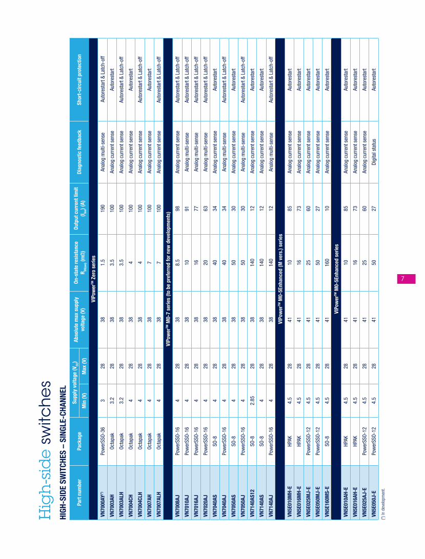
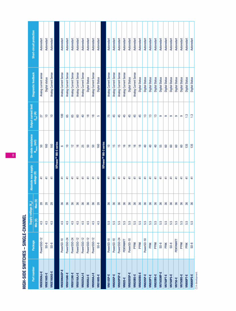
High-side switchesST’s offer of fully-protected automotive high-side switches (HSDs) is the broadest in the market. Having an unmatched range of packages, on-resistances, number of output channels and diagnostic options, HSDs are able to drive resistive, inductive and capacitive grounded loads in compliance with the stringent safety and reliability requirements of automotive applications. Based on its proprietary VIPower™ technology, ST’s high-side switches have 3 V and 5 V CMOS compatible I/Os for control and vertical mosfet for the power outputs, and are the perfect companions for a microcontroller.
VIPowerTM M0-7 SERIESThe M0-7 series is the ultimate VIPower product generation, born to deliver the widest range of on-state resistance and number of channels with full pin-to-pin compatibility in the smallest packages. Further application benefits are:
• Best-in-class EMI performance, short-circuit protection and robustness
• Lower quiescent current
• Precise load-current, battery voltage and device temperature analog feedback
VIPowerTM M0-5 SERIESThe M0-5 series is the largest family of VIPower high-side switches developed to drive any kind of automotive load.
The devices are equipped with digital status or analog current sense feedback. Further advantages are available in the M0-5Enhanced options:
• Extended load compatibility due to higher current limitation
• Instantaneous diagnosis of short-to-ground or overload
• OFF-state diagnosis for the analog current sense option (‘E’ types)
Introduction

5
VIPowerTM Zero seriesST’s VIPowerTM Zero series offers innovative and high-performance protected switches for driving high power applications.This series covers today’s growing demand for intelligent power devices able to drive and protect high-power loads such as those used in high-current fan motors, heaters and protected battery lines in electrical power distribution systems.
KEY FEATURES• Complete family of low on-resistance protected solutions
• Output re-activation during reverse polarity
• State-of-the-art and adaptable protection strategy
• Sophisticated diagnostics
• Cold-cranking capability (device option)
• Device option with extended diagnostics capability cover a wide range of load currents
VN7007AH
VN7007ALH
VN7004CLH
VN7000AY
VN7004CH
7 mΩ 4 mΩ 3 mΩ 1.5 mΩ
FEAT
URE
SET
VN7003ALH
VN7003AH
VND7004AY
VIPower M0-7 Typical Feature Set• Unsurpassed Protection Strategy based on proprietary IPs• Advanced Diagnostic with accurate Output Sensing• Output re-activation under Reverse Polarity
Programmable Protection Enabling exible and adaptable protection strategy based on Output Auto-reactivation / Latch-off under overload conditions
Extended CurrentSensingFor application requiring extra precision in output sensing and covering a wider current range
Very Low-VoltageOperationSuitable for applications requiring to keep active equipment even during extreme low battery (Cold Cranking condition - LV124 compliance)
Door actuator drivers with embedded Power ManagementThe new L99DZ1x0 Family brings higher performances in the Door Zone Applications: novel devices embed, in the same package, Power management power supply functionality (including various standby modes, as well as LIN and HS CAN physical communication layers) together with all the Actuators for main Door loads. The two low-drop voltage regulators of the devices supply the system microcontroller and external peripheral loads such as sensors and provide enhanced system standby functionality with programmable local and remote wake-up capability.
An advanced driver provides logic and protection for external Mosfet transistors in H-bridge, or Dual Half Bridge, configuration . Other features include integrated bridges for double door-lock control, mirror fold, and mirror-axis control, together with high-side drivers for bulbs and LEDs control. In addition, high-side drivers allow small resistive loads driving for increasing system integration level. An additional gate drive can control an external MOSFET in high-side configuration to supply a resistive load connected to GND (e.g. mirror heater). An electro-chromic mirror glass can be controlled using the integrated SPI-driven module in conjunction with an external MOS transistor.
All the embedded outputs come with protection and supervision features such as Current Monitor (only for High Side outputs), Openload, Overcurrent, Thermal Warming, Thermal Shutdown (increased up to 175 °C as mimimum threshold) and Themal Expiration. Devices include two Fail safe low side switches that are intended to be used to turn off the gates of the external high-side MOSFETs in the power window h-bridge if a fatal error happens. The ST standard SPI interface (4.0) allows control and diagnosis of the device and enables generic software development.

6
Motor control ICsTaking advantage from the proprietary VIPower™ silicon technology and from miniaturized packaging solutions, the VNH family of fully integrated H-bridges combines in single packages a matchless level of diagnostic and sensing capabilities together with solid protections and robust vertical structure MOSFETs making automotive DC motor control applications - ranging from a few up to hundreds of watts - more robust and compact.
Power management ICs for automotive systemsPower management ICs come with enhanced power supply functions and they include various standby modes as well as LIN and HS-CAN (also with HS-CAN supporting Partial Network) physical communication layers. They offer two low-drop voltage regulators to supply the system microcontroller and external peripheral loads (sensors) and provide superior system standby functionality with programmable local and remote wake-up capabilities. Other features, like high-side and low-side drivers or operational amplifiers, are embedded to increase the system integration level.What’s more, ST has a wide multifunctional voltage regulator portfolio that meets all automotive infotainment needs. They are protected against load dump and support battery voltage variations and transients, providing multiple linear or switching voltage outputs, with or without an I²C bus, and have a very low standby quiescent current.
Door module driversST’s door module drivers family is designed for state-of-the-art automotive door electronics. Devices are characterized by a scalable actuator driving concept, which includes packages and software specially designed to satisfy a wide range of door module variants. Drivers support all regular door module loads such as lock motors, mirror levelling and foldering, defroster, electro-chromic mirror glass, window lift and several lighting functions from incandescent bulbs to LEDs.
Low-side switchesFully-protected, low-side switches safely drive resistive, inductive and capacitive loads with one terminal connected to the battery, in compliance with the stringent safety and reliability requirements of automotive applications.ST’s low-side switches offer a power output in addition to control and diagnostic function in one single chip and are available with both single- and dual-channel options.
OMNIFET IIIBuilt in the VIPower M0-5 technology, the OMNIFET III series addresses a broad range of applications in tiny packages, delivering protection and diagnostic features. Key application benefits include:
• Low stand-by current consumption
• Overload and open-load diagnostic
OMNIFET AND OMNIFET IIST offers a wide portfolio of low-side switches suitable for any kind of automotive load and applications rated up to 70 V.
• Optimized EMI performances
• Enhanced short circuit robustness
7
Hig
h-s
ide
switc
he
sHI
GH-S
IDE
SWIT
CHES
– S
INGL
E-CH
ANNE
L
Part
num
ber
Pack
age
Supp
ly v
olta
ge (V
CC)
Abso
lute
max
sup
ply
volta
ge (V
)On
-sta
te re
sist
ance
R DS
(on) (m
Ω)
Outp
ut c
urre
nt li
mit
(I lim) (
A)Di
agno
stic
feed
back
Shor
t-ci
rcui
t pro
tect
ion
Min
(V)
Max
(V)
VIPo
wer
TM Z
ero
serie
s
VN70
00AY
(*)
Pow
erSS
O‑36
328
381.
519
0An
alog
mul
ti‑se
nse
Aut
ores
tart
& La
tch‑
off
VN70
03AH
Octa
pak
3.2
2838
3.5
100
Anal
og c
urre
nt s
ense
Auto
rest
art
VN70
03AL
HOc
tapa
k3.
228
383.
510
0An
alog
cur
rent
sen
seAu
tore
star
t & L
atch
‑off
VN70
04CH
Octa
pak
428
384
100
Anal
og c
urre
nt s
ense
Auto
rest
art
VN70
04CL
HOc
tapa
k4
2838
410
0An
alog
cur
rent
sen
seAu
tore
star
t & L
atch
‑off
VN70
07AH
Octa
pak
428
387
100
Anal
og c
urre
nt s
ense
Auto
rest
art
VN70
07AL
HOc
tapa
k4
2838
710
0An
alog
cur
rent
sen
seAu
tore
star
t & L
atch
‑off
VIPo
wer
TM M
0-7
serie
s (to
be
pref
erre
d fo
r new
dev
elop
men
ts)
VN70
08AJ
Pow
erSS
O‑16
428
388.
598
Anal
og c
urre
nt s
ense
Auto
rest
art &
Lat
ch‑o
ff
VN70
10AJ
Pow
erSS
O‑16
428
3810
91An
alog
mul
ti‑se
nse
Auto
rest
art &
Lat
ch‑o
ff
VN70
16AJ
Pow
erSS
O‑16
428
3816
77An
alog
mul
ti‑se
nse
Auto
rest
art &
Lat
ch‑o
ff
VN70
20AJ
Pow
erSS
O‑16
428
3820
63An
alog
mul
ti‑se
nse
Auto
rest
art &
Lat
ch‑o
ff
VN70
40AS
SO‑8
428
3840
34An
alog
cur
rent
sen
seAu
tore
star
t
VN70
40AJ
Pow
erSS
O‑16
428
3840
34An
alog
mul
ti‑se
nse
Auto
rest
art &
Lat
ch‑o
ff
VN70
50AS
SO‑8
428
3850
30An
alog
cur
rent
sen
seAu
tore
star
t
VN70
50AJ
Pow
erSS
O‑16
428
3850
30An
alog
mul
ti‑se
nse
Auto
rest
art &
Lat
ch‑o
ff
VN71
40AS
12SO
‑82.
8528
3814
012
Anal
og c
urre
nt s
ense
Auto
rest
art
VN71
40AS
SO‑8
428
3814
012
Anal
og c
urre
nt s
ense
Auto
rest
art
VN71
40AJ
Pow
erSS
O‑16
428
3814
012
Anal
og m
ulti‑
sens
eAu
tore
star
t & L
atch
‑off
VIPo
wer
TM M
0-5E
nhan
ced
(M v
ers.
) ser
ies
VN5E
010M
H-E
HPAK
4.5
2841
1085
Anal
og c
urre
nt s
ense
Auto
rest
art
VN5E
016M
H-E
HPAK
4.5
2841
1673
Anal
og c
urre
nt s
ense
Auto
rest
art
VN5E
025M
J-E
Pow
erSS
O‑12
4.5
2841
2560
Anal
og c
urre
nt s
ense
Auto
rest
art
VN5E
050M
J-E
Pow
erSS
O‑12
4.5
2841
5027
Anal
og c
urre
nt s
ense
Auto
rest
art
VN5E
160M
S-E
SO‑8
4.5
2841
160
10An
alog
cur
rent
sen
seAu
tore
star
t
VIPo
wer
TM M
0-5E
nhan
ced
serie
s
VN5E
010A
H-E
HPAK
4.5
2841
1085
Anal
og c
urre
nt s
ense
Auto
rest
art
VN5E
016A
H-E
HPAK
4.5
2841
1673
Anal
og c
urre
nt s
ense
Auto
rest
art
VN5E
025A
J-E
Pow
erSS
O‑12
4.5
2841
2560
Anal
og c
urre
nt s
ense
Auto
rest
art
VN5E
050J
-EPo
wer
SSO‑
124.
528
4150
27Di
gita
l sta
tus
Auto
rest
art
(*) In
dev
elop
men
t.
8
HIGH
-SID
E SW
ITCH
ES –
SIN
GLE-
CHAN
NEL
Part
num
ber
Pack
age
Supp
ly v
olta
ge (V
CC)
Abso
lute
max
sup
ply
volta
ge (V
)On
-sta
te re
sist
ance
R DS
(on) (m
Ω)
Outp
ut c
urre
nt li
mit
(I lim) (
A)Di
agno
stic
feed
back
Shor
t-ci
rcui
t pro
tect
ion
Min
(V)
Max
(V)
VN5E
050A
J-E
Pow
erSS
O‑12
4.5
2841
5027
Anal
og c
urre
nt s
ense
Auto
rest
art
VN5E
160S
-ESO
‑84.
528
4116
010
Digi
tal s
tatu
sAu
tore
star
t
VN5E
160A
S-E
SO‑8
4.5
2841
160
10An
alog
Cur
rent
Sen
seAu
tore
star
t
VIPo
wer
TM M
0-5
serie
s
VN5E
006A
SP-E
Pow
erSO
‑10
4.5
3641
610
0An
alog
Cur
rent
Sen
seAu
tore
star
t
VN50
10AK
-EPo
wer
SSO‑
244.
536
4110
65An
alog
Cur
rent
Sen
seAu
tore
star
t
VN50
12AK
-EPo
wer
SSO‑
244.
536
4112
65An
alog
Cur
rent
Sen
seAu
tore
star
t
VN50
16AJ
-EPo
wer
SSO‑
124.
536
4116
60An
alog
Cur
rent
Sen
seAu
tore
star
t
VN50
25AJ
-EPo
wer
SSO‑
124.
536
4125
40An
alog
Cur
rent
Sen
seAu
tore
star
t
VN50
50J-
EPo
wer
SSO‑
124.
536
4150
18Di
gita
l Sta
tus
Auto
rest
art
VN50
50AJ
-EPo
wer
SSO‑
124.
536
4150
18An
alog
Cur
rent
Sen
seAu
tore
star
t
VN51
60S-
ESO
‑84.
528
4116
05
Digi
tal S
tatu
sAu
tore
star
t
VIPo
wer
TM M
0-3
serie
s
VN61
0SP-
EPo
wer
SO‑1
05.
536
4110
75An
alog
Cur
rent
Sen
seAu
tore
star
t
VN92
0SP-
EPo
wer
SO‑1
05.
536
4115
45An
alog
Cur
rent
Sen
seAu
tore
star
t
VN92
0PEP
-EPo
wer
SSO‑
245.
536
4115
45An
alog
Cur
rent
Sen
seAu
tore
star
t
VN92
0-E
PENT
AWAT
T5.
536
4116
45An
alog
Cur
rent
Sen
seAu
tore
star
t
VN92
0DSP
-EPo
wer
SO‑1
05.
536
4116
45Di
gita
l Sta
tus
Auto
rest
art
VN92
0B5-
EP²
PAK
5.5
3641
1645
Anal
og C
urre
nt S
ense
Auto
rest
art
VN92
0DB5
-EP²
PAK
5.5
3641
1845
Digi
tal S
tatu
sAu
tore
star
t
VN82
0SP-
EPo
wer
SO‑1
05.
536
4140
13Di
gita
l Sta
tus
Auto
rest
art
VN82
0PT-
EPP
AK5.
536
4140
13Di
gita
l Sta
tus
Auto
rest
art
VN82
0B5-
EP²
PAK
5.5
3641
4013
Digi
tal S
tatu
sAu
tore
star
t
VN75
0SM
P-E
SO‑8
5.5
3641
559
Digi
tal S
tatu
sAu
tore
star
t
VN75
0PT-
EPP
AK5.
536
4160
9Di
gita
l Sta
tus
Auto
rest
art
VN75
0PS-
ESO
‑85.
536
4160
9Di
gita
l Sta
tus
Auto
rest
art
VN75
0-E
PENT
AWAT
T5.
536
4160
9Di
gita
l Sta
tus
Auto
rest
art
VN75
0B5-
EP²
PAK
5.5
3641
609
Digi
tal S
tatu
sAu
tore
star
t
VN80
0PT-
EPP
AK5.
536
4113
51.
3Di
gita
l Sta
tus
Auto
rest
art
VN80
0PS-
ESO
‑85.
536
4113
51.
3Di
gita
l Sta
tus
Auto
rest
art
(*) In
dev
elop
men
t.
9
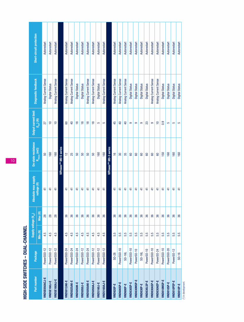
HIGH
-SID
E SW
ITCH
ES –
DUA
L-CH
ANNE
L
Part
num
ber
Pack
age
Supp
ly v
olta
ge (V
CC)
Abso
lute
max
sup
ply
volta
ge (V
)On
-sta
te re
sist
ance
R DS
(on) (m
Ω)
Outp
ut c
urre
nt li
mit
(I lim) (
A)Di
agno
stic
feed
back
Shor
t-ci
rcui
t pro
tect
ion
Min
(V)
Max
(V)
VIPo
wer
TM Z
ero
serie
s
VND7
004A
YPo
wer
SSO‑
364
2838
410
0An
alog
Mul
ti‑Se
nse
Auto
rest
art &
Lat
ch‑o
ff
VIPo
wer
TM M
0-7
serie
s (to
be
pref
erre
d fo
r new
dev
elop
men
ts)
VND7
012A
YPo
wer
SSO‑
364
2838
1275
Anal
og M
ulti‑
Sens
eAu
tore
star
t & L
atch
‑off
VND7
020A
JPo
wer
SSO‑
164
2838
2263
Anal
og C
urre
nt S
ense
Auto
rest
art &
Lat
ch‑o
ff
VND7
030A
JPo
wer
SSO‑
164
2838
3156
Anal
og C
urre
nt S
ense
Auto
rest
art &
Lat
ch‑o
ff
VND7
040A
JPo
wer
SSO‑
164
2838
4034
Anal
og M
ulti‑
Sens
eAu
tore
star
t & L
atch
‑off
VND7
050A
J12
Pow
erSS
O‑12
2.85
2838
5030
Anal
og M
ulti‑
Sens
eAu
tore
star
t
VND7
050A
JPo
wer
SSO‑
164
2838
5030
Anal
og M
ulti‑
Sens
eAu
tore
star
t & L
atch
‑off
VND7
140A
J12
Pow
erSS
O‑12
2.85
2838
140
12An
alog
Cur
rent
Sen
seAu
tore
star
t
VND7
140A
JPo
wer
SSO‑
164
2838
140
12An
alog
Mul
ti‑Se
nse
Auto
rest
art &
Lat
ch‑o
ff
VIPo
wer
TM M
0-5E
nhan
ced
(M v
ers.
) ser
ies
VND5
E008
MY-
EPo
wer
SSO‑
364.
528
418
85An
alog
Cur
rent
Sen
seAu
tore
star
t
VND5
E012
MY-
EPo
wer
SSO‑
364.
528
4112
74An
alog
Cur
rent
Sen
seAu
tore
star
t
VND5
E025
MK-
EPo
wer
SSO‑
244.
528
4125
60An
alog
Cur
rent
Sen
seAu
tore
star
t
VND5
E050
MCK
-EPo
wer
SSO‑
244.
528
4150
27An
alog
Cur
rent
Sen
seAu
tore
star
t
VND5
E050
MCJ
-EPo
wer
SSO‑
124.
528
4150
27An
alog
Cur
rent
Sen
seAu
tore
star
t
VND5
E160
MJ-
EPo
wer
SSO‑
124.
528
4116
010
Anal
og C
urre
nt S
ense
Auto
rest
art
VIPo
wer
TM M
0-5E
nhan
ced
serie
s
VND5
E004
C30-
EM
ultiP
ower
SO‑3
04.
528
414
100
Anal
og C
urre
nt S
ense
Auto
rest
art
VND5
E004
A-E
PQFN
4.5
2841
410
0An
alog
Cur
rent
Sen
seAu
tore
star
t
VND5
E006
ASP-
EPo
wer
SO‑1
64.
528
416
100
Anal
og C
urre
nt S
ense
Auto
rest
art
VND5
E008
AY-E
Pow
erSS
O‑36
4.5
2841
885
Anal
og C
urre
nt S
ense
Auto
rest
art
VND5
E008
ASP-
EPo
wer
SO‑1
64.
528
418
85An
alog
Cur
rent
Sen
seAu
tore
star
t
VND5
E012
AY-E
Pow
erSS
O‑36
4.5
2841
1274
Anal
og C
urre
nt S
ense
Auto
rest
art
VND5
E025
NAY-
EPo
wer
SSO‑
364.
528
4125
60An
alog
Cur
rent
Sen
seAu
tore
star
t
VND5
E025
LK-E
Pow
erSS
O‑24
4.5
2841
2540
Anal
og C
urre
nt S
ense
Auto
rest
art
VND5
E025
BK-E
Pow
erSS
O‑24
4.5
2841
2560
Anal
og C
urre
nt S
ense
Auto
rest
art
VND5
E025
AY-E
Pow
erSS
O‑36
4.5
2841
2547
Anal
og C
urre
nt S
ense
Auto
rest
art
VND5
E025
AK-E
Pow
erSS
O‑24
4.5
2841
2560
Anal
og C
urre
nt S
ense
Auto
rest
art
VND5
E050
K-E
Pow
erSS
O‑24
4.5
2841
5027
Digi
tal S
tatu
sAu
tore
star
t
VND5
E050
J-E
Pow
erSS
O‑12
4.5
2841
5027
Digi
tal S
tatu
sAu
tore
star
t
VND5
E050
ACK-
EPo
wer
SSO‑
244.
528
4150
27An
alog
Cur
rent
Sen
seAu
tore
star
t
10
HIGH
-SID
E SW
ITCH
ES –
DUA
L-CH
ANNE
L
Part
num
ber
Pack
age
Supp
ly v
olta
ge (V
CC)
Abso
lute
max
sup
ply
volta
ge (V
)On
-sta
te re
sist
ance
R DS
(on) (m
Ω)
Outp
ut c
urre
nt li
mit
(I lim) (
A)Di
agno
stic
feed
back
Shor
t-ci
rcui
t pro
tect
ion
Min
(V)
Max
(V)
VND5
E050
ACJ-
EPo
wer
SSO‑
124.
528
4150
27An
alog
Cur
rent
Sen
seAu
tore
star
t
VND5
E160
J-E
Pow
erSS
O‑12
4.5
2841
160
10Di
gita
l Sta
tus
Auto
rest
art
VND5
E160
AJ-E
Pow
erSS
O‑12
4.5
2841
160
10An
alog
Cur
rent
Sen
seAu
tore
star
t
VIPo
wer
TM M
0-5
serie
s
VND5
012A
K-E
Pow
erSS
O‑24
4.5
3641
1260
Anal
og C
urre
nt S
ense
Auto
rest
art
VND5
025A
K-E
Pow
erSS
O‑24
4.5
3641
2540
Anal
og C
urre
nt S
ense
Auto
rest
art
VND5
050K
-EPo
wer
SSO‑
244.
536
4150
18Di
gita
l Sta
tus
Auto
rest
art
VND5
050J
-EPo
wer
SSO‑
124.
536
4150
18Di
gita
l Sta
tus
Auto
rest
art
VND5
050A
K-E
Pow
erSS
O‑24
4.5
3641
5018
Anal
og C
urre
nt S
ense
Auto
rest
art
VND5
050A
J-E
Pow
erSS
O‑12
4.5
3641
5018
Anal
og C
urre
nt S
ense
Auto
rest
art
VND5
160J
-EPo
wer
SSO‑
124.
536
4116
05
Digi
tal S
tatu
sAu
tore
star
t
VND5
160A
J-E
Pow
erSS
O‑12
4.5
3641
160
5An
alog
Cur
rent
Sen
seAu
tore
star
t
VIPo
wer
TM M
0-3
serie
s
VND9
20P-
ESO
‑28
5.5
3641
1645
Anal
og C
urre
nt S
ense
Auto
rest
art
VND6
00SP
-EPo
wer
SSO‑
105.
536
4130
40An
alog
Cur
rent
Sen
seAu
tore
star
t
VND6
00P-
ESO
‑16L
5.5
3641
3540
Anal
og C
urre
nt S
ense
Auto
rest
art
VND8
30SP
-EPo
wer
SSO‑
105.
536
4160
9Di
gita
l Sta
tus
Auto
rest
art
VND8
30M
SP-E
Pow
erSO
‑10
5.5
3641
609
Digi
tal S
tatu
sAu
tore
star
t
VND8
30P-
ESO
‑16L
5.5
3641
609
Digi
tal S
tatu
sAu
tore
star
t
VND8
30LS
P-E
Pow
erSO
‑10
5.5
3641
6023
Digi
tal S
tatu
sAu
tore
star
t
VND8
30AS
P-E
Pow
erSS
O‑10
5.5
3641
609
Anal
og C
urre
nt S
ense
Auto
rest
art
VND8
30AE
P-E
Pow
erSO
‑24
5.5
3641
6010
Anal
og C
urre
nt S
ense
Auto
rest
art
VND8
10M
SP-E
Pow
erSS
O‑10
5.5
3641
150
0.9
Digi
tal S
tatu
sAu
tore
star
t
VND8
10SP
-EPo
wer
SSO‑
205.
536
4116
05
Digi
tal S
tatu
sAu
tore
star
t
VND8
10PE
P-E
Pow
erSO
‑12
5.5
3641
160
5Di
gita
l Sta
tus
Auto
rest
art
VND8
10P-
ESO
‑16
5.5
3641
160
5Di
gita
l Sta
tus
Auto
rest
art
(*) In
dev
elop
men
t.
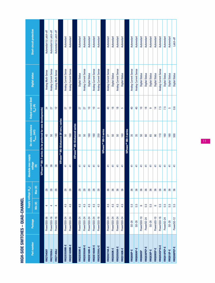
11
HIGH
-SID
E SW
ITCH
ES –
QUA
D-CH
ANNE
L
Part
num
ber
Pack
age
Supp
ly v
olta
ge (V
CC)
Abso
lute
max
sup
ply
volta
ge(V
)
On-s
tate
resi
stan
ceR DS
(on) (m
Ω)
Outp
ut c
urre
nt li
mit
(I lim) (
A)Di
gita
l sta
tus
Shor
t-ci
rcui
t pro
tect
ion
Min
(V)
Max
(V)
VIPo
wer
TM M
0-7
serie
s (to
be
pref
erre
d fo
r new
dev
elop
men
ts)
VNQ7
040A
YPo
wer
SSO‑
364
2838
4034
Anal
og M
ulti‑
Sens
eAu
tore
star
t & L
atch
‑off
VNQ7
050A
JPo
wer
SSO‑
164
2838
5027
Anal
og C
urre
nt S
ense
Auto
rest
art &
Lat
ch‑o
ff
VNQ7
140A
JPo
wer
SSO‑
164
2838
140
12An
alog
Mul
ti‑Se
nse
Auto
rest
art &
Lat
ch‑o
ff
VIPo
wer
TM M
0-5E
nhan
ced
(M v
ers.
) ser
ies
VNQ5
E050
MK-
EPo
wer
SSO‑
244.
528
4150
27An
alog
Cur
rent
Sen
seAu
tore
star
t
VNQ5
E160
MK-
EPo
wer
SSO‑
244.
528
4116
010
Anal
og C
urre
nt S
ense
Auto
rest
art
VIPo
wer
TM M
0-5E
nhan
ced
serie
s
VNQ5
E050
K-E
Pow
erSS
O‑24
4.5
2841
5027
Digi
tal S
tatu
sAu
tore
star
t
VNQ5
E050
AK-E
Pow
erSS
O‑24
4.5
2841
5027
Anal
og C
urre
nt S
ense
Auto
rest
art
VNQ5
E160
K-E
Pow
erSS
O‑24
4.5
2841
160
10Di
gita
l Sta
tus
Auto
rest
art
VNQ5
E160
AK-E
Pow
erSS
O‑24
4.5
2841
160
10An
alog
Cur
rent
Sen
seAu
tore
star
t
VNQ5
E250
AJ-E
Pow
erSS
O‑16
4.5
2841
250
5An
alog
Cur
rent
Sen
seAu
tore
star
t
VIPo
wer
TM M
0-5
serie
s
VNQ5
027A
K-E
Pow
erSS
O‑24
4.5
3641
2740
Anal
og C
urre
nt S
ense
Auto
rest
art
VNQ5
050K
-EPo
wer
SSO‑
244.
536
4150
18Di
gita
l Sta
tus
Auto
rest
art
VNQ5
050A
K-E
Pow
erSS
O‑24
4.5
3641
5018
Anal
og C
urre
nt S
ense
Auto
rest
art
VNQ5
160K
-EPo
wer
SSO‑
244.
536
4116
05
Digi
tal S
tatu
sAu
tore
star
t
VIPo
wer
TM M
0-3
serie
s
VNQ6
00P-
ESO
‑28
5.5
3641
3540
Anal
og C
urre
nt S
ense
Auto
rest
art
VNQ6
00AP
-ESO
‑28
5.5
3641
3540
Anal
og C
urre
nt S
ense
Auto
rest
art
VNQ6
60SP
Pow
erSS
O‑10
636
4150
10Di
gita
l Sta
tus
Auto
rest
art
VNQ8
30PE
P-E
Pow
erSO
‑24
5.5
3641
6018
Digi
tal S
tatu
sAu
tore
star
t
VNQ8
30P-
ESO
‑28
5.5
3641
659
Digi
tal S
tatu
sAu
tore
star
t
VNQ6
90SP
-EPo
wer
sSO‑
106
3641
9014
Digi
tal S
tatu
sAu
tore
star
t
VNQ0
5XSP
16-E
Pow
erSS
O‑16
5.5
3641
110
7.5
Anal
og C
urre
nt S
ense
Auto
rest
art
VNQ8
10PE
P-E
Pow
erSO
‑24
5.5
3641
160
7.5
Digi
tal S
tatu
sAu
tore
star
t
VNQ8
10P-
ESO
‑28
5.5
3641
160
5Di
gita
l Sta
tus
Auto
rest
art
VNQ5
00PE
P-E
Pow
erSO
‑12
5.5
3641
500
0.6
Digi
tal S
tatu
sLa
tch‑
off
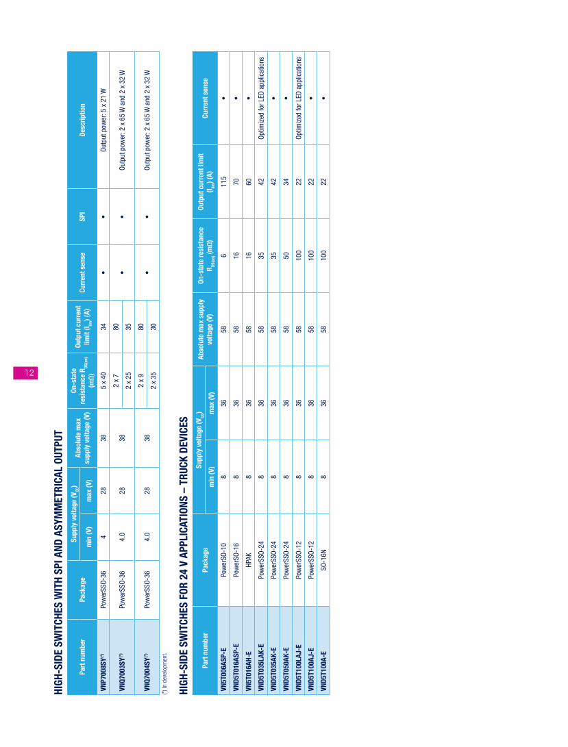
12
HIGH
-SID
E SW
ITCH
ES W
ITH
SPI A
ND A
SYM
MET
RICA
L OU
TPUT
Part
num
ber
Pack
age
Supp
ly v
olta
ge (V
CC)
Abso
lute
max
su
pply
vol
tage
(V)
On-s
tate
re
sist
ance
RDS
(on)
(mΩ
)
Outp
ut c
urre
nt
limit
(I lim) (
A)Cu
rren
t sen
seSP
IDe
scrip
tion
min
(V)
max
(V)
VNP7
008S
Y(*)
Pow
erSS
O‑36
428
385
x 40
34•
•Ou
tput
pow
er: 5
x 2
1 W
VNQ7
003S
Y(*)
Pow
erSS
O‑36
4.0
2838
2 x
780
••
Outp
ut p
ower
: 2 x
65
W a
nd 2
x 3
2 W
2 x
2535
VNQ7
004S
Y(*)
Pow
erSS
O‑36
4.0
2838
2 x
980
••
Outp
ut p
ower
: 2 x
65
W a
nd 2
x 3
2 W
2 x
3530
(*) In
dev
elop
men
t.
HIGH
-SID
E SW
ITCH
ES F
OR 2
4 V
APPL
ICAT
IONS
– T
RUCK
DEV
ICES
Part
num
ber
Pack
age
Supp
ly v
olta
ge (V
CC)
Abso
lute
max
sup
ply
volta
ge (V
)On
-sta
te re
sist
ance
R DS
(on) (m
Ω)
Outp
ut c
urre
nt li
mit
(I lim) (
A)Cu
rren
t sen
sem
in (V
)m
ax (V
)
VN5T
006A
SP-E
Pow
erSO
‑10
836
586
115
•
VND5
T016
ASP-
EPo
wer
SO‑1
68
3658
1670
•
VN5T
016A
H-E
HPAK
836
5816
60•
VND5
T035
LAK-
EPo
wer
SSO‑
248
3658
3542
Optim
ized
for L
ED a
pplic
atio
ns
VND5
T035
AK-E
Pow
erSS
O‑24
836
5835
42•
VND5
T050
AK-E
Pow
erSS
O‑24
836
5850
34•
VND5
T100
LAJ-
EPo
wer
SSO‑
128
3658
100
22Op
timiz
ed fo
r LED
app
licat
ions
VND5
T100
AJ-E
Pow
erSS
O‑12
836
5810
022
•
VND5
T100
A-E
SO‑1
6N8
3658
100
22•
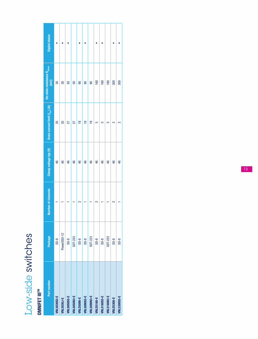
13
Low
-sid
e sw
itch
es
OMNI
FET
IIITM
Part
num
ber
Pack
age
Num
ber o
f cha
nnel
s Cl
amp
volta
ge ty
p (V
)Dr
ain
curr
ent l
imit
(I lim) (
A)On
-sta
te re
sist
ance
RDS
(on)
(mΩ
)Di
gita
l sta
tus
VNL5
030S
5-E
SO‑8
146
3530
•
VNL5
030J
-EPo
wer
SSO‑
121
4635
30•
VNL5
050S
5-E
SO‑8
146
2750
•
VNL5
050N
3-E
SOT‑
223
146
2750
VNLD
5090
-ESO
‑82
4618
90•
VNL5
090S
5-E
SO‑8
146
1890
•
VNL5
090N
3-E
SOT‑
223
146
1890
VNLD
5160
-ESO
‑82
465
160
•
VNL5
160S
5-E
SO‑8
146
516
0•
VNL5
160N
3-E
SOT‑
223
146
516
0
VNLD
5300
-ESO
‑82
462
300
•
VNL5
300S
5-E
SO‑8
146
230
0•
14
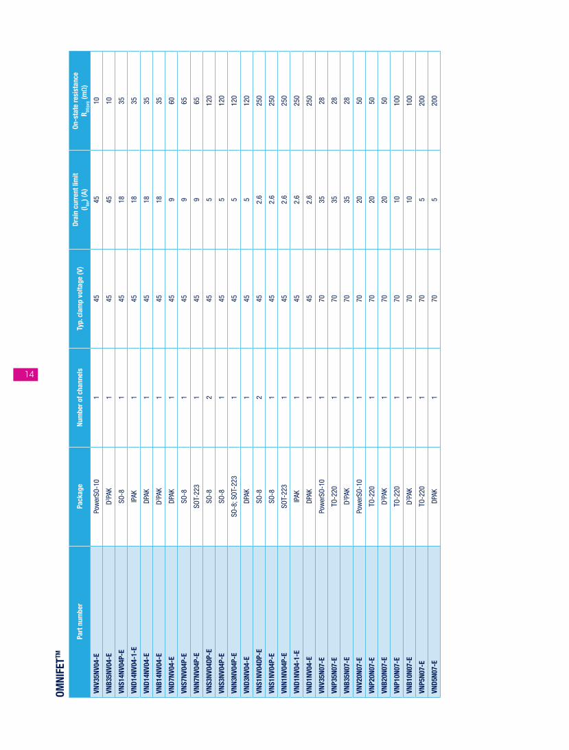
OMNI
FETTM
Part
num
ber
Pack
age
Num
ber o
f cha
nnel
sTy
p. c
lam
p vo
ltage
(V)
Drai
n cu
rren
t lim
it (I lim
) (A)
On-s
tate
resi
stan
ce
R DS(o
n) (m
Ω)
VNV3
5NV0
4-E
Pow
erSO
‑10
145
4510
VNB3
5NV0
4-E
D2 PAK
145
4510
VNS1
4NV0
4P-E
SO‑8
145
1835
VND1
4NV0
4-1-
EIP
AK1
4518
35
VND1
4NV0
4-E
DPAK
145
1835
VNB1
4NV0
4-E
D2 PAK
145
1835
VND7
NV04
-EDP
AK1
459
60
VNS7
NV04
P-E
SO‑8
145
965
VNN7
NV04
P-E
SOT‑
223
145
965
VNS3
NV04
DP-E
SO‑8
245
512
0
VNS3
NV04
P-E
SO‑8
145
512
0
VNN3
NV04
P-E
SO‑8
; SOT
‑223
145
512
0
VND3
NV04
-EDP
AK1
455
120
VNS1
NV04
DP-E
SO‑8
245
2.6
250
VNS1
NV04
P-E
SO‑8
145
2.6
250
VNN1
NV04
P-E
SOT‑
223
145
2.6
250
VND1
NV04
-1-E
IPAK
145
2.6
250
VND1
NV04
-EDP
AK1
452.
625
0
VNV3
5N07
-EPo
wer
SO‑1
01
7035
28
VNP3
5N07
-ETO
‑220
170
3528
VNB3
5N07
-ED2 P
AK1
7035
28
VNV2
0N07
-EPo
wer
SO‑1
01
7020
50
VNP2
0N07
-ETO
‑220
170
2050
VNB2
0N07
-ED2 P
AK1
7020
50
VNP1
0N07
-ETO
‑220
170
1010
0
VNB1
0N07
-ED2 P
AK1
7010
100
VNP5
N07-
ETO
‑220
170
520
0
VND5
N07-
EDP
AK1
705
200
15
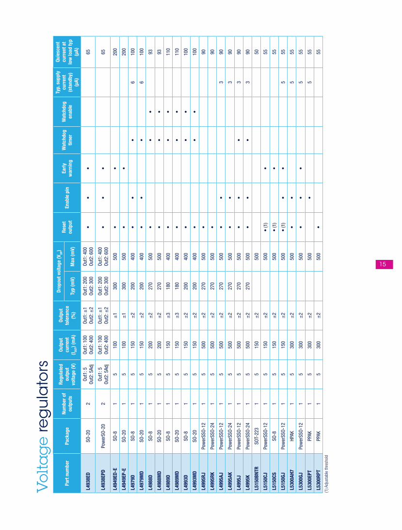
Vol
tag
e re
gu
lato
rsPa
rt n
umbe
rPa
ckag
eNu
mbe
r of
outp
uts
Regu
late
d ou
tput
vo
ltage
(V)
Outp
ut
curr
ent
(I OUT)
(mA)
Outp
ut
tole
ranc
e (%
)
Drop
out v
olta
ge (V
DP)
Rese
t ou
tput
Enab
le p
inEa
rly
war
ning
Wat
chdo
g tim
erW
atch
dog
enab
le
Typ.
sup
ply
curr
ent
(sta
ndby
)(μ
A)
Quie
scen
t cu
rren
t at
low
load
typ
(µA)
Typ
(mV)
Max
(mV)
L493
8ED
SO‑2
02
Out1
: 5Ou
t2: 5
Adj
Out1
: 100
Out2
: 400
Out1
: ±1
Out2
: ±2
Out1
: 200
Out2
: 300
Out1
: 400
Out2
: 600
••
•65
L493
8EPD
Pow
erSO
‑20
2Ou
t1: 5
Out2
: 5Ad
jOu
t1: 1
00Ou
t2: 4
00Ou
t1: ±
1Ou
t2: ±
2Ou
t1: 2
00Ou
t2: 3
00Ou
t1: 4
00Ou
t2: 6
00•
••
65
L494
9ED-
ESO
‑81
510
0±
130
050
0•
•20
0
L494
9EP-
ESO
‑20
15
100
±1
300
500
••
200
L497
9DSO
‑81
515
0±
220
040
0•
••
610
0
L497
9MD
SO‑2
01
515
0±
220
040
0•
••
610
0
L498
8DSO
‑81
520
0±
227
050
0•
••
93
L498
8MD
SO‑2
01
520
0±
227
050
0•
••
93
L498
9DSO
‑81
515
0±
318
040
0•
••
110
L498
9MD
SO‑2
01
515
0±
318
040
0•
••
110
L499
3DSO
‑81
515
0±
220
040
0•
••
100
L499
3MD
SO‑2
01
515
0±
220
040
0•
••
100
L499
5RJ
Pow
erSS
O‑12
15
500
±2
270
500
•90
L499
5RK
Pow
erSS
O‑24
15
500
±2
270
500
•90
L499
5AJ
Pow
erSS
O‑12
15
500
±2
270
500
••
390
L499
5AK
Pow
erSS
O‑24
15
500
±2
270
500
••
390
L499
5JPo
wer
SSO‑
121
550
0±
227
050
0•
••
390
L499
5KPo
wer
SSO‑
241
550
0±
227
050
0•
••
390
L515
0BNT
RSO
T‑22
31
515
0±
250
050
L515
0CJ
Pow
erSS
O‑12
15
150
±2
500
• (1
)•
55
L515
0CS
SO‑8
15
150
±2
500
• (1
)•
55
L515
0GJ
Pow
erSS
O‑12
15
150
±2
500
• (1
)•
•5
55
L530
0AH7
HPAK
15
300
±2
500
••
555
L530
0GJ
Pow
erSS
O‑12
15
300
±2
500
••
•5
55
L530
0EPT
PPAK
15
300
±2
500
•5
55
L530
0RPT
PPAK
15
300
±2
500
•55
(1) A
djus
tabl
e th
resh
old
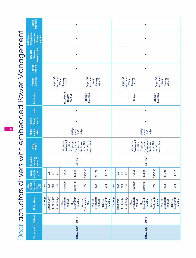
16
Doo
r a
ctu
ato
rs d
rive
rs w
ith e
mb
ed
de
d P
ow
er M
an
ag
em
en
t
Part
num
ber
Pack
age
Driv
er s
tage
s
Max
on
-sta
te
resi
stan
ce
R DS(o
n)
(mΩ
)
Curr
ent
limita
tion
I lim (A
)
Exte
nded
oper
ativ
e ra
nge
(V)
PWM
co
ntro
l
Mot
or
cont
rol
driv
er
Elec
tro-
chro
me
mirr
orHe
ater
Tran
scei
vers
Volta
ge
regu
lato
rsTh
erm
al
clus
ters
Auto
LED
di
mm
ing
com
pens
atio
n
A/D
Volta
ge-
tem
pera
ture
co
nver
tion
ther
mal
cl
uste
rs
Ther
mal
Ex
pira
tion
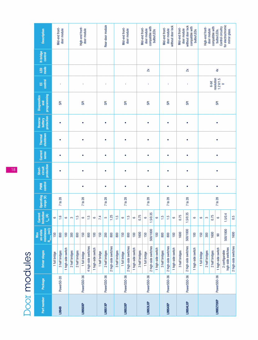
L99D
Z100
GPLQ
FP64
1 Fu
ll Br
idge
300
3
3.5(*
) to
28
Inde
pend
ent
PWM
con
trol
for a
ll th
e Ou
tput
s, 4
pr
ogra
mm
able
fre
quen
cies
and
10
cha
nnel
s w
ith 1
0 bi
t re
solu
tion.
2
inte
rnal
tim
ers
H‑br
idge
or
dua
l Ha
lf br
idge
••
HS‑C
AN w
ith
Sele
ctiv
e W
ake
Up
LIN
2.2a
/ SA
E J2
602
Outp
ut 5
V1M
ax c
urre
nt
250m
AAc
cura
cy
±2
% (*
*)
Outp
ut 5
V2M
ax c
urre
nt
50m
AAc
cura
cy
±3
% (*
*)
••
••
2 Ha
lf Br
idge
s20
000.
5
1 Ha
lf Br
idge
100
7.5
1 Ha
lf Br
idge
150
7.5
1 R DS
(on)
Confi
gura
ble
Hi
gh S
ide
500/
1600
1.5/
0.35
1 R DS
(on)
Co
nfigu
rabl
e
High
Sid
e80
0/16
000.
8/0.
35
3 Cu
rren
t Co
nfigu
rabl
e Hi
gh
Side
2000
0.15
/0.3
5
1 Cu
rren
t Co
nfigu
rabl
e
High
Sid
e20
000.
25/0
.5
4 Cu
rren
t Co
nfigu
rabl
e
High
Sid
e50
000.
15/0
.25
L99D
Z100
GLQ
FP64
1 Fu
ll Br
idge
300
3
3.5(*
) to
28
Inde
pend
ent
PWM
con
trol
for a
ll th
e Ou
tput
s, 4
pr
ogra
mm
able
fre
quen
cies
and
10
cha
nnel
s w
ith 1
0 bi
t re
solu
tion.
2
inte
rnal
tim
ers
H‑br
idge
or
dua
l Ha
lf br
idge
••
HS‑C
AN
LIN
2.2a
/ SA
E J2
602
Outp
ut 5
V1M
ax c
urre
nt
250m
AAc
cura
cy
±2
% (*
*)
Outp
ut 5
V2M
ax c
urre
nt
50m
AAc
cura
cy
±3
% (*
*)
••
••
2 Ha
lf Br
idge
s20
000.
5
1 Ha
lf Br
idge
100
7.5
1 Ha
lf Br
idge
150
7.5
1 R DS
(on)
Co
nfigu
rabl
e
High
Sid
e50
0/16
001.
5/0.
35
1 R DS
(on)
Confi
gura
ble
Hi
gh S
ide
800/
1600
0.8/
0.35
3 Cu
rren
t Co
nfigu
rabl
e
High
Sid
e20
000.
15/0
.35
1 Cu
rren
t Co
nfigu
rabl
e
High
Sid
e20
000.
25/0
.5
4 Cu
rren
t Co
nfigu
rabl
e
High
Sid
e50
000.
15/0
.25
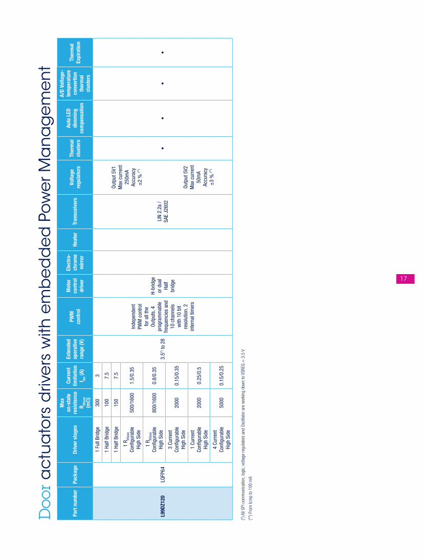
17
Part
num
ber
Pack
age
Driv
er s
tage
s
Max
on
-sta
te
resi
stan
ce
R DS(o
n)
(mΩ
)
Curr
ent
limita
tion
I lim (A
)
Exte
nded
oper
ativ
e ra
nge
(V)
PWM
co
ntro
l
Mot
or
cont
rol
driv
er
Elec
tro-
chro
me
mirr
orHe
ater
Tran
scei
vers
Volta
ge
regu
lato
rsTh
erm
al
clus
ters
Auto
LED
di
mm
ing
com
pens
atio
n
A/D
Volta
ge-
tem
pera
ture
co
nver
tion
ther
mal
cl
uste
rs
Ther
mal
Ex
pira
tion
L99D
Z120
LQFP
64
1 Fu
ll Br
idge
300
3
3.5(*
) to
28
Inde
pend
ent
PWM
con
trol
for a
ll th
e Ou
tput
s, 4
pr
ogra
mm
able
fre
quen
cies
and
10
cha
nnel
s w
ith 1
0 bi
t re
solu
tion.
2
inte
rnal
tim
ers
H‑br
idge
or
dua
l Ha
lf br
idge
LIN
2.2a
/ SA
E J2
602
Outp
ut 5
V1M
ax c
urre
nt
250m
AAc
cura
cy
±2
% (*
*)
Outp
ut 5
V2M
ax c
urre
nt
50m
AAc
cura
cy
±3
% (*
*)
••
••
1 Ha
lf Br
idge
100
7.5
1 Ha
lf Br
idge
150
7.5
1 R DS
(on)
Co
nfigu
rabl
e Hi
gh S
ide
500/
1600
1.5/
0.35
1 R DS
(on)
Co
nfigu
rabl
e Hi
gh S
ide
800/
1600
0.8/
0.35
3 Cu
rren
t Co
nfigu
rabl
e Hi
gh S
ide
2000
0.15
/0.3
5
1 Cu
rren
t Co
nfigu
rabl
e Hi
gh S
ide
2000
0.25
/0.5
4 Cu
rren
t Co
nfigu
rabl
e Hi
gh S
ide
5000
0.15
/0.2
5
(*) A
ll SP
I com
mun
icat
ion,
logi
c, v
olta
ge re
gula
tors
and
Osc
illato
r are
wor
king
dow
n to
VSR
EG =
3.5
V
(**) F
rom
Icm
p to
100
mA
Doo
r a
ctu
ato
rs d
rive
rs w
ith e
mb
ed
de
d P
ow
er M
an
ag
em
en
t
18
Doo
r m
od
ule
sPa
rt n
umbe
rPa
ckag
eDr
iver
sta
ges
Max
on
-sta
te
resi
stan
ce
R DS(o
n) (m
Ω)
Curr
ent
limita
tion
I lim (A
)
Oper
atin
g ra
nge
(V)
PWM
co
ntro
l
Shor
t-ci
rcui
t pr
otec
tion
Curr
ent
sens
eTh
erm
al
shut
dow
n
Reve
rse
batte
ry
prot
ectio
n
Diag
nost
ics
and
pr
ogra
mm
ing
EC
cont
rol
LED
mod
eH-
brid
ge
cont
rol
Desc
riptio
n
L994
9Po
wer
SO‑2
0
1 fu
ll br
idge
15
06
7 to
28
•
••
•SP
I‑
Mid
‑end
fron
t‑do
or m
odul
e3
half
brid
ges
80
01.
6
1 hi
gh‑s
ide
switc
h
100
6
L995
0XP
Pow
erSS
O‑36
2 ha
lf br
idge
s
300
3
7 to
28
••
••
•SP
I‑
High
‑end
fron
t‑do
or m
odul
e
2 ha
lf br
idge
s
800
1.5
1 fu
ll br
idge
15
06
4 hi
gh‑s
ide
switc
hes
800
1.5
1 hi
gh‑s
ide
switc
h
100
6
L995
1XP
Pow
erSS
O‑36
1 ha
lf br
idge
150
7.4
7 to
28
••
••
•SP
I‑
Rear
‑doo
r mod
ule
2 ha
lf br
idge
s
200
5
2 hi
gh‑s
ide
switc
hes
800
1.25
L995
3XP
Pow
erSS
O‑36
3 ha
lf br
idge
s
800
1.5
7 to
28
••
••
•SP
I‑
Mid
‑end
fron
t‑do
or m
odul
e
1 fu
ll br
idge
150
6
2 hi
gh‑s
ide
switc
hes
800
1.5
1 hi
gh‑s
ide
switc
h
100
6
L995
3LXP
Pow
erSS
O‑36
3 ha
lf br
idge
s
1600
0.75
7 to
28
••
••
• SP
I‑
2x
Mid
‑end
fron
t‑do
or m
odul
e co
mpa
tible
with
bu
lbs/
LEDs
1 fu
ll br
idge
150
6
2 hi
gh‑s
ide
switc
hes
500/
1800
1.5/
0.35
1 hi
gh‑s
ide
switc
h
100
6
L995
4XP
Pow
erSS
O‑36
3 ha
lf br
idge
s80
01.
5
7 to
28
• •
••
•SP
I‑
Mid
‑end
fron
t‑do
or m
odul
e w
ithou
t doo
r loc
k 2
high
‑sid
e sw
itche
s80
01.
5
1 hi
gh‑s
ide
switc
h
100
6
L995
4LXP
Pow
erSS
O‑36
3 ha
lf br
idge
s16
000.
75
7 to
28
••
••
•SP
I‑
2x
Mid
‑end
fron
t‑do
or m
odul
e w
ithou
t doo
r loc
k co
mpa
tible
with
bu
lbs/
LEDs
2 hi
gh‑s
ide
switc
hes
500/
1800
1.5/
0.35
1 hi
gh‑s
ide
switc
h
100
6
L99D
Z70X
PPo
wer
SSO‑
36
1 fu
ll br
idge
15
06
7 to
28
••
••
•SP
I
6‑bi
t re
solu
tion
1.2
V/1.
5 V
4x
High
‑end
fron
t‑do
or m
odul
e co
mpa
tible
with
bu
lbs/
LEDs
. Co
ntro
l circ
uitr
y fo
r ele
ctro
chro
mic
m
irror
gla
ss.
2 ha
lf br
idge
s30
03
2 ha
lf br
idge
s 16
000.
75
1 hi
gh‑s
ide
switc
h
906
2 co
nfigu
rabl
e
high
‑sid
e sw
itche
s 50
0/18
001.
5/0.
4
2 hi
gh‑s
ide
switc
hes
1600
0.5
19
Part
num
ber
Pack
age
Driv
er s
tage
s
Max
on
-sta
te
resi
stan
ce
R DS(o
n) (m
Ω)
Curr
ent
limita
tion
I lim (A
)
Oper
atin
g ra
nge
(V)
PWM
co
ntro
l
Shor
t-ci
rcui
t pr
otec
tion
Curr
ent
sens
eTh
erm
al
shut
dow
n
Reve
rse
batte
ry
prot
ectio
n
Diag
nost
ics
and
pr
ogra
mm
ing
EC
cont
rol
LED
mod
eH-
brid
ge
cont
rol
Desc
riptio
n
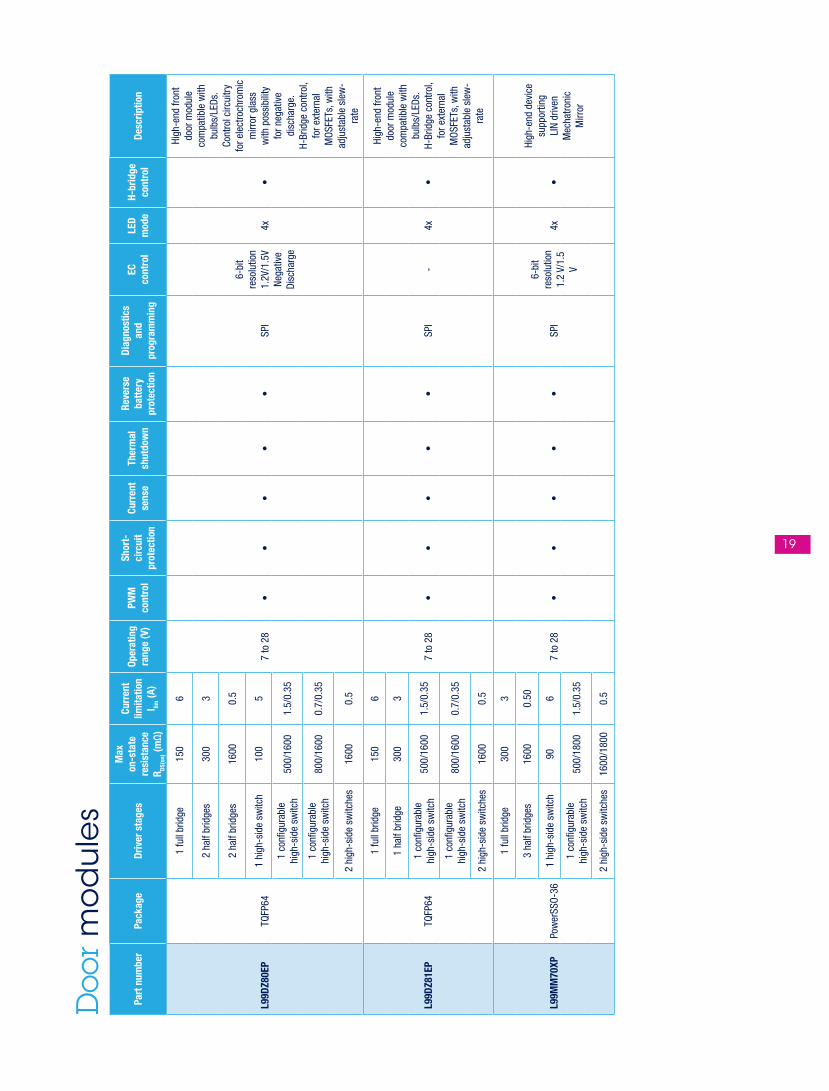
L99D
Z80E
PTQ
FP64
1 fu
ll br
idge
15
06
7 to
28
•
•
•
•
•
SPI
6‑bi
t re
solu
tion
1.2V
/1.5
V Ne
gativ
e Di
scha
rge
4x•
High
‑end
fron
t do
or m
odul
e co
mpa
tible
with
bu
lbs/
LEDs
. Co
ntro
l circ
uitr
y fo
r ele
ctro
chro
mic
m
irror
gla
ss
with
pos
sibi
lity
for n
egat
ive
disc
harg
e.
H‑Br
idge
con
trol,
for e
xter
nal
MOS
FETs
, with
ad
just
able
sle
w‑
rate
2 ha
lf br
idge
s30
03
2 ha
lf br
idge
s 16
000.
5
1 hi
gh‑s
ide
switc
h
100
5
1 co
nfigu
rabl
e
high
‑sid
e sw
itch
500/
1600
1.5/
0.35
1 co
nfigu
rabl
e
high
‑sid
e sw
itch
800/
1600
0.7/
0.35
2 hi
gh‑s
ide
switc
hes
1600
0.5
L99D
Z81E
PTQ
FP64
1 fu
ll br
idge
15
06
7 to
28
•
•
•
•
•
SPI
‑4x
•
High
‑end
fron
t do
or m
odul
e co
mpa
tible
with
bu
lbs/
LEDs
. H‑
Brid
ge c
ontro
l, fo
r ext
erna
l M
OSFE
Ts, w
ith
adju
stab
le s
lew
‑ra
te
1 ha
lf br
idge
300
3
1 co
nfigu
rabl
e
high
‑sid
e sw
itch
500/
1600
1.5/
0.35
1 co
nfigu
rabl
e
high
‑sid
e sw
itch
800/
1600
0.7/
0.35
2 hi
gh‑s
ide
switc
hes
1600
0.5
L99M
M70
XPPo
wer
SSO‑
36
1 fu
ll br
idge
30
03
7 to
28
•
•
•
•
•
SPI
6‑bi
t re
solu
tion
1.2
V/1.
5 V
4x•
High
‑end
dev
ice
supp
ortin
g LI
N dr
iven
M
echa
troni
c M
irror
3 ha
lf br
idge
s16
000.
50
1 hi
gh‑s
ide
switc
h90
6
1 co
nfigu
rabl
e
high
‑sid
e sw
itch
500/
1800
1.5/
0.35
2 hi
gh‑s
ide
switc
hes
1600
/180
00.
5
Doo
r m
od
ule
s
20
Pow
er m
an
ag
em
en
t fo
r au
tom
otiv
e s
yste
ms
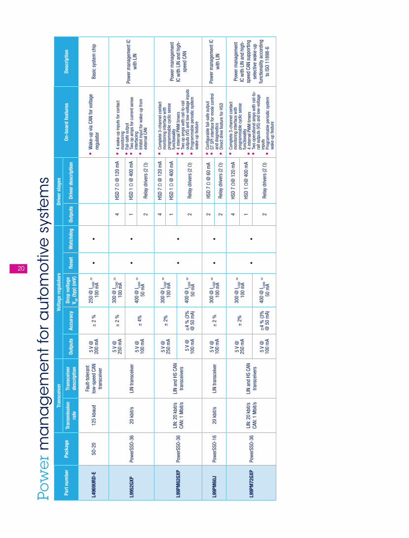
Part
num
ber
Pack
age
Tran
scei
ver
Volta
ge re
gula
tors
Driv
er s
tage
sOn
-boa
rd fe
atur
esDe
scrip
tion
Tran
smis
sion
ra
teTr
ansc
eive
r de
scrip
tion
Outp
uts
Accu
racy
Drop
vol
tage
V DP
(typ
) (m
V)Re
set
Wat
chdo
gOu
tput
sDr
iver
des
crip
tion
L496
9URD
-E
SO‑2
012
5 kb
aud
Faul
t‑to
lera
nt
low
‑spe
ed C
AN
trans
ceiv
er
5 V
@
200
mA
± 2
%
250
@ I LO
AD =
10
0 m
A•
•
•
Wak
e‑up
via
CAN
for v
olta
ge
regu
lato
rBa
sic
syst
em c
hip
L995
2GXP
Po
wer
SSO‑
3620
kbi
t/sLI
N tra
nsce
iver
5 V
@
250
mA
± 2
%30
0 @
I LOAD
=
100
mA
•
•
4HS
D 7
Ω @
120
mA
• 4
wak
e‑up
inpu
ts fo
r con
tact
m
onito
ring
• Fa
il‑sa
fe o
utpu
t •
Two
op a
mps
for c
urre
nt s
ense
in
terfa
cing
• In
hibi
t inp
ut fo
r wak
e‑up
from
ex
tern
al C
AN
Pow
er m
anag
emen
t IC
with
LIN
5 V
@
100
mA
± 4
%
400
@ I LO
AD =
50
mA
1HS
D 1
Ω @
400
mA
2Re
lay
driv
ers
(2 Ω
)
L99P
M62
GXP
Pow
erSS
O‑36
LIN:
20
kbit/
sCA
N: 1
Mbi
t/sLI
N an
d HS
CAN
tra
nsce
iver
s
5 V
@
250
mA
± 2
%30
0 @
I LOAD
=
100
mA
•
•
4HS
D 7
Ω @
120
mA
• Co
mpl
ete
3‑ch
anne
l con
tact
m
onito
ring
inte
rface
with
pr
ogra
mm
able
cyc
lic s
ense
fu
nctio
nalit
y•
4 in
tern
al P
WM
tim
ers
• Tw
o op
am
ps w
ith ra
il‑to
‑rai
l ou
tput
s (V
S) a
nd lo
w‑v
olta
ge in
puts
• Pr
ogra
mm
able
per
iodi
c sy
stem
w
ake‑
up fe
atur
e
Pow
er m
anag
emen
t IC
with
LIN
and
hig
h‑sp
eed
CAN
1HS
D 1
Ω @
400
mA
5 V
@
100
mA
±4
% (3
%
@ 5
0 m
A)40
0 @
I LOAD
=
50 m
A2
Rela
y dr
iver
s (2
Ω)
L99P
M60
J Po
wer
SSO‑
1620
kbi
t/sLI
N tra
nsce
iver
5
V @
10
0 m
A±
2 %
300
@ I LO
AD =
10
0 m
A•
•
2
HSD
7 Ω
@ 6
0 m
A •
Confi
gura
ble
fail‑
safe
out
put
• ST
SPI
inte
rface
for m
ode
cont
rol
and
diag
nost
ics
• Di
rect
driv
e fe
atur
e fo
r HSD
Pow
er m
anag
emen
t IC
with
LIN
2Re
lay
driv
ers
(2 Ω
)
L99P
M72
GXP
Pow
erSS
O‑36
LIN:
20
kbit/
sCA
N: 1
Mbi
t/sLI
N an
d HS
CAN
tra
nsce
iver
s
5 V
@
250
mA
± 2
%30
0 @
I LOAD
=
100
mA
•
•
4HS
D 7
Ω@
120
mA
• Co
mpl
ete
3‑ch
anne
l con
tact
m
onito
ring
inte
rface
with
pr
ogra
mm
able
cyc
lic s
ense
fu
nctio
nalit
y•
4 in
tern
al P
WM
tim
ers
• Tw
o op
erat
iona
l am
ps w
ith ra
il‑to
‑ra
il ou
tput
s (V
S) a
nd lo
w‑v
olta
ge
inpu
ts•
Prog
ram
mab
le p
erio
dic
syst
em
wak
e‑up
feat
ure
Pow
er m
anag
emen
t IC
with
LIN
and
hig
h‑sp
eed
CAN
supp
ortin
g se
lect
ive
wak
e‑up
fu
nctio
nalit
y ac
cord
ing
to IS
O 11
898‑
6
1HS
D 1
Ω@
400
mA
5 V
@
100
mA
±4
% (3
%
@ 5
0 m
A)40
0 @
I LOAD
=
50 m
A2
Rela
y dr
iver
s (2
Ω)
21
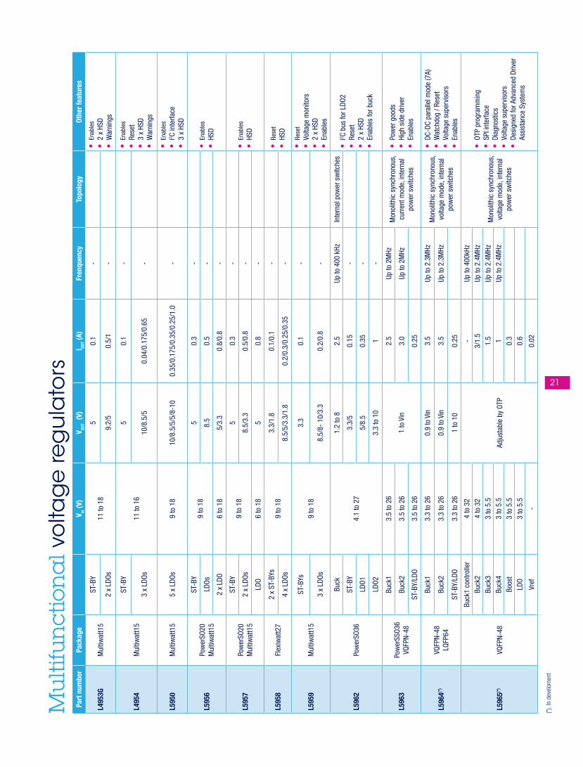
Mu
ltifu
nct
ion
al v
olta
ge
reg
ula
tors
Part
num
ber
Pack
age
V in (V
)V OU
T (V
)I OU
T (A)
Fren
quen
cyTo
polo
gyOt
her f
eatu
res
L495
3GM
ultiw
att1
5ST
‑BY
11 to
18
50.
1‑
• En
able
s•
2 x
HSD
• W
arni
ngs
2 x
LDOs
9.2/
50.
5/1
‑
L495
4M
ultiw
att1
5
ST‑B
Y
11 to
16
50.
1‑
• En
able
s•
Rese
t•
3 x
HSD
• W
arni
ngs
3 x
LDOs
10/8
.5/5
0.04
/0.1
75/0
.65
‑
L595
0M
ultiw
att1
55
x LD
Os9
to 1
810
/8.5
/5/5
/8‑1
00.
35/0
.175
/0.3
5/0.
25/1
.0‑
• En
able
s•
I2 C in
terfa
ce•
3 x
HSD
L595
6Po
wer
SO20
M
ultiw
att1
5
ST‑B
Y9
to 1
85
0.3
‑•
Enab
les
• HS
DLD
Os8.
50.
5‑
2 x
LDO
6 to
18
5/3.
30.
8/0.
8‑
L595
7Po
wer
SO20
M
ultiw
att1
5
ST‑B
Y9
to 1
85
0.3
‑•
Enab
les
• HS
D2
x LD
Os8.
5/3.
30.
5/0.
8‑
LDO
6 to
18
50.
8‑
L595
8Fl
exiw
att2
72
x ST
‑BYs
9 to
18
3.3/
1.8
0.1/
0.1
‑•
Rese
t•
HSD
4 x
LDOs
8.5/
5/3.
3/1.
80.
2/0.
3/0.
25/0
.35
‑
L595
9M
ultiw
att1
5ST
‑BYs
9 to
18
3.3
0.1
‑•
Rese
t•
Volta
ge m
onito
rs•
2 x
HSD
• En
able
s3
x LD
Os8.
5/8‑
10/
3.3
0.2/
0.8
‑
L596
2Po
wer
SO36
Buck
4.1
to 2
7
1.2
to 8
2.5
Up to
400
kHz
Inte
rnal
pow
er s
witc
hes
• I2 C
bus
for L
DO2
• Re
set
• 2
x HS
D•
Enab
les
for b
uck
ST‑B
Y3.
3/5
0.15
‑
LDO1
5/8.
50.
35‑
LDO2
3.3
to 1
01
‑
L596
3Po
wer
SSO3
6 VQ
FPN‑
48
Buck
13.
5 to
26
1 to
Vin
2.5
Up to
2M
HzM
onol
ithic
syn
chro
nous
, cu
rren
t mod
e, in
tern
al
pow
er s
witc
hes
• Po
wer
goo
ds•
High
sid
e dr
iver
• En
able
sBu
ck2
3.5
to 2
63.
0Up
to 2
MHz
ST‑B
Y/LD
O3.
5 to
26
0.25
L596
4(*)
VQFP
N‑48
LQFP
64
Buck
13.
3 to
26
0.9
to V
in3.
5Up
to 2
.3M
HzM
onol
ithic
syn
chro
nous
, vo
ltage
mod
e, in
tern
al
pow
er s
witc
hes
• DC
‑DC
para
llel m
ode
(7A)
• W
atch
dog
/ Res
et•
Volta
ge s
uper
viso
rs•
Enab
les
Buck
23.
3 to
26
0.9
to V
in3.
5Up
to 2
.3M
Hz
ST‑B
Y/LD
O3.
3 to
26
1 to
10
0.25
L596
5(*)
VQFP
N‑48
Buck
1 co
ntro
ller
4 to
32
Adju
stab
le b
y OT
P
‑Up
to 4
00kH
z
Mon
olith
ic s
ynch
rono
us,
volta
ge m
ode,
inte
rnal
po
wer
sw
itche
s
• OT
P pr
ogra
mm
ing
• SP
I int
erfa
ce•
Diag
nost
ics
• Vo
ltage
sup
ervi
sors
• De
sign
ed fo
r Adv
ance
d Dr
iver
As
sist
ance
Sys
tem
s
Buck
24
to 3
23/
1.5
Up to
2.4
MHz
Buck
33
to 5
.51.
5Up
to 2
.4M
HzBu
ck4
3 to
5.5
1Up
to 2
.4M
HzBo
ost
3 to
5.5
0.3
LDO
3 to
5.5
0.6
Vref
‑0.
02
(*). I
n de
velo
men
t
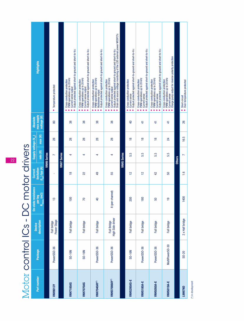
22
Mot
or c
on
trol I
Cs
- DC
mo
tor d
rive
rs
Part
num
ber
Pack
age
Devi
ce
desc
riptio
n
On-s
tate
resi
stan
ce
per l
egR DS
(on) (m
Ω)
Curr
ent
limita
tion
(I lim) t
yp (A
)
Supp
ly v
olta
ge (V
CC)
Abso
lute
m
ax s
uppl
y vo
ltage
(V)
High
light
sm
in (V
)m
ax (V
)
VNH9
Ser
ies
VNH9
013Y
Pow
erSS
O‑36
Full
brid
ge
Pow
er S
tage
13‑
728
80•
Tem
pera
ture
pro
tect
ed
VNH7
Ser
ies
VNH7
100A
SSO
‑16N
Full
brid
ge10
018
428
38•
Cros
s‑co
nduc
tion
prot
ectio
n•
PWM
ope
ratio
ns u
p to
20
kHz
• Cu
rren
t sen
se o
utpu
t•
Outp
ut p
rote
cted
aga
inst
sho
rt‑to
gro
und
and
shor
t‑to
‑Vcc
VNH7
070A
SSO
‑16N
Full
brid
ge70
224
2838
• Cr
oss‑
cond
uctio
n pr
otec
tion
• PW
M o
pera
tions
up
to 2
0 kH
z•
Curr
ent s
ense
out
put
• Ou
tput
pro
tect
ed a
gain
st s
hort‑
to g
roun
d an
d sh
ort‑
to‑V
cc
VNH7
040A
Y(*)
Pow
erSS
O‑36
Full
brid
ge40
494
2838
• Cr
oss‑
cond
uctio
n pr
otec
tion
• PW
M o
pera
tions
up
to 2
0 kH
z•
Mul
tisen
se o
utpu
t•
Outp
ut p
rote
cted
aga
inst
sho
rt‑to
gro
und
and
shor
t‑to
‑Vcc
VNHD
7008
AY(*
)Po
wer
SSO‑
36Fu
ll Br
idge
Hi
gh S
ide
driv
er8
(per
cha
nnel
)55
428
38
• Cr
oss‑
cond
uctio
n pr
otec
tion
• PW
M o
pera
tions
up
to 2
0 kH
z•
Curr
ent s
ense
out
put
• Ou
tput
pro
tect
ed a
gain
st s
hort‑
to g
roun
d an
d sh
ort‑
to‑V
cc•
Drai
n an
d so
urce
vol
tage
mon
itorin
g of
the
LSD
exte
rnal
pow
er M
OSFE
Ts
VNH5
Ser
ies
VNH5
200A
S-E
SO‑1
6NFu
ll br
idge
200
125.
518
40•
Cros
s‑co
nduc
tion
prot
ectio
n•
Curr
ent s
ense
• Ou
tput
pro
tect
ed a
gain
st s
hort‑
to‑g
roun
d an
d sh
ort‑
to‑V
cc
VNH5
180A
-EPo
wer
SSO‑
36Fu
ll br
idge
180
125.
518
41•
Cros
s‑co
nduc
tion
prot
ectio
n•
PWM
ope
ratio
ns u
p to
20
kHz
• Cu
rren
t sen
se•
Outp
ut p
rote
cted
aga
inst
sho
rt‑to
‑gro
und
and
shor
t‑to
‑Vcc
VNH5
050A
-EPo
wer
SSO‑
36Fu
ll br
idge
5042
5.5
1841
• Cr
oss‑
cond
uctio
n pr
otec
tion
• PW
M o
pera
tions
up
to 2
0 kH
z•
Curr
ent s
ense
• Ou
tput
pro
tect
ed a
gain
st s
hort‑
to‑g
roun
d an
d sh
ort‑
to‑V
cc
VNH5
019A
-EM
ultiP
ower
SO‑3
0Fu
ll br
idge
1950
5.5
2441
• Cr
oss‑
cond
uctio
n pr
otec
tion
• PW
M o
pera
tions
up
to 2
0 kH
z•
Curr
ent s
ense
• Ch
arge
pum
p ou
tput
for r
ever
se‑p
olar
ity p
rote
ctio
n
Othe
rs
L999
7ND
SO‑2
02
x Ha
lf br
idge
1400
1.6
716
.526
• Sh
ort‑
circ
uit
• Ov
er‑t
empe
ratu
re p
rote
cted
(*) In
dev
elop
men
t
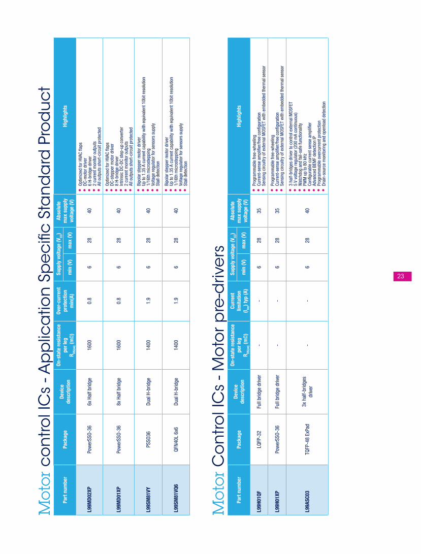
23
Mot
or c
on
trol I
Cs
- Ap
plic
atio
n S
pe
cifi
c S
tan
da
rd P
rod
uc
tPa
rt n
umbe
rPa
ckag
eDe
vice
de
scrip
tion
On-s
tate
resi
stan
ce
per l
egR DS
(on) (m
Ω)
Over
-cur
rent
pr
otec
tion
min
(A)
Supp
ly v
olta
ge (V
CC)
Abso
lute
m
ax s
uppl
y vo
ltage
(V)
High
light
sm
in (V
)m
ax (V
)
L99M
D02X
PPo
wer
SSO‑
366x
Hal
f brid
ge16
000.
86
2840
• Op
timiz
ed fo
r HVA
C fla
ps•
DC‑m
otor
driv
er•
6 H‑
brid
ge d
river
• 2
curr
ent m
onito
r out
puts
• Al
l out
puts
sho
rt‑ci
rcui
t pro
tect
ed
L99M
D01X
PPo
wer
SSO‑
368x
Hal
f brid
ge16
000.
86
2840
• Op
timiz
ed fo
r HVA
C fla
ps•
DC‑s
tepp
er m
otor
driv
er•
8 H‑
brid
ge d
river
• In
trins
ic D
C‑DC
ste
p‑up
con
verte
r•
2 cu
rren
t mon
itor o
utpu
ts•
All o
utpu
ts s
hort‑
circ
uit p
rote
cted
L99S
M81
VYPS
SO36
Dual
H‑b
ridge
1400
1.9
628
40
• Bi
pola
r ste
pper
mot
or d
river
• Up
to 1
.35
A cu
rren
t cap
abili
ty w
ith e
quiv
alen
t 10b
it re
solu
tion
• 1/
16th
mic
rost
eppi
ng•
Volta
ge re
gula
tor f
or s
enso
rs s
uppl
y•
Stal
l det
ectio
n
L99S
M81
VQ6
QFN4
0L 6
x6Du
al H
‑brid
ge14
001.
96
2840
• Bi
pola
r ste
pper
mot
or d
river
• Up
to 1
.35
A cu
rren
t cap
abili
ty w
ith e
quiv
alen
t 10b
it re
solu
tion
• 1/
16th
mic
rost
eppi
ng•
Volta
ge re
gula
tor f
or s
enso
rs s
uppl
y•
Stal
l det
ectio
n
Mot
or C
on
trol I
Cs
- Mo
tor p
re-d
rive
rsPa
rt n
umbe
rPa
ckag
eDe
vice
de
scrip
tion
On-s
tate
resi
stan
ce
per l
egR DS
(on) (m
Ω)
Curr
ent
limita
tion
(I lim) t
yp (A
)
Supp
ly v
olta
ge (V
CC)
Abso
lute
m
ax s
uppl
y vo
ltage
(V)
High
light
sm
in (V
)m
ax (V
)
L99H
01QF
LQFP
‑32
Full
brid
ge d
river
‑‑
628
35•
Prog
ram
mab
le fr
ee‑w
heel
ing
• Cu
rren
t‑se
nse
ampl
ifier
/free
con
figur
atio
n•
Sens
ing
circ
uitr
y of
ext
erna
l MOS
FET
with
em
bedd
ed th
erm
al s
enso
r
L99H
01XP
Pow
erSS
O‑36
Full
brid
ge d
river
‑‑
628
35•
Prog
ram
mab
le fr
ee‑w
heel
ing
• Cu
rren
t‑se
nse
ampl
ifier
/free
con
figur
atio
n•
Sens
ing
circ
uitr
y of
ext
erna
l MOS
FET
with
em
bedd
ed th
erm
al s
enso
r
L99A
SC03
TQFP
‑48
ExPa
d3x
hal
f‑br
idge
sdr
iver
‑‑
628
40
• 3
half‑
brid
ges
driv
er to
con
trol e
xter
nal M
OSFE
T•
5 V
volta
ge re
gula
tor (
200
mA
cont
inuo
us)
• W
atch
dog
and
fail‑
safe
func
tiona
lity
• PW
M u
p to
80
kHz
• Co
nfigu
rabl
e cu
rren
t sen
se a
mpl
ifier
• Ad
vanc
ed B
EMF
dete
ctio
n IP
• Pr
ogra
mm
able
ove
rcur
rent
pro
tect
ion
• Dr
ain‑
sour
ce m
onito
ring
and
open
load
det
ectio
n
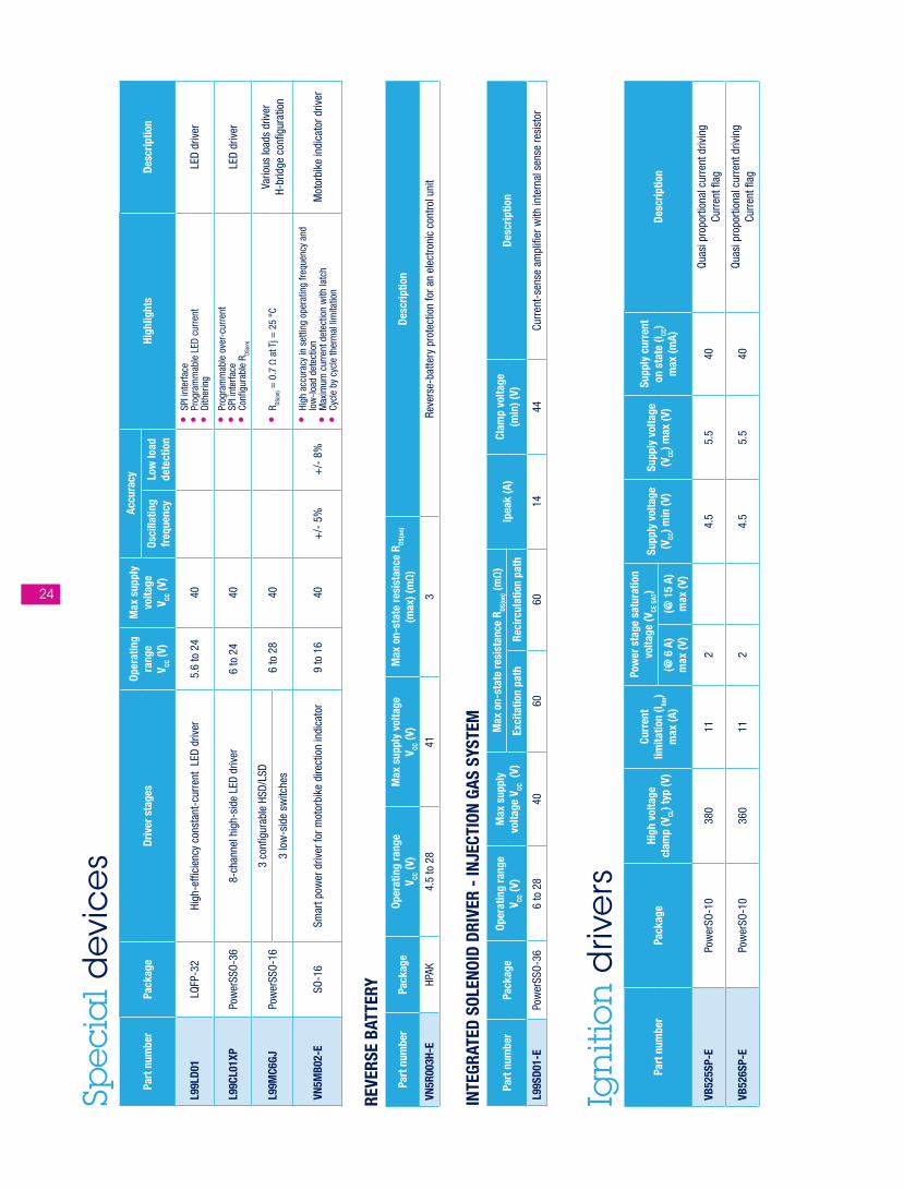
24
Spec
ial d
evic
es
Part
num
ber
Pack
age
Driv
er s
tage
sOp
erat
ing
rang
e V CC
(V)
Max
sup
ply
volta
ge
V CC (V
)
Accu
racy
High
light
sDe
scrip
tion
Osci
llatin
g fr
eque
ncy
Low
load
de
tect
ion
L99L
D01
LQFP
‑32
High
‑effi
cien
cy c
onst
ant‑
curr
ent
LED
driv
er5.
6 to
24
40•
SPI i
nter
face
• Pr
ogra
mm
able
LED
cur
rent
• Di
ther
ing
LED
driv
er
L99C
L01X
PPo
wer
SSO‑
368‑
chan
nel h
igh‑
side
LED
driv
er6
to 2
440
• Pr
ogra
mm
able
ove
r‑cu
rren
t•
SPI i
nter
face
• Co
nfigu
rabl
e R DS
(on)
LED
driv
er
L99M
C6GJ
Pow
erSS
O‑16
3
confi
gura
ble
HSD/
LSD
6 to
28
40
• R DS
(on) =
0.7
Ω a
t Tj =
25
°C
Vario
us lo
ads
driv
er
H‑br
idge
con
figur
atio
n3
low
‑sid
e sw
itche
s
VN5M
B02-
ESO
‑16
Smar
t pow
er d
river
for m
otor
bike
dire
ctio
n in
dica
tor
9 to
16
40
+/‑
5%
+/‑
8%
• Hi
gh a
ccur
acy
in s
ettin
g op
erat
ing
frequ
ency
and
lo
w‑lo
ad d
etec
tion
• M
axim
um c
urre
nt d
etec
tion
with
latc
h•
Cycl
e by
cyc
le th
erm
al li
mita
tion
Mot
orbi
ke in
dica
tor d
river
REVE
RSE
BATT
ERY
Part
num
ber
Pack
age
Oper
atin
g ra
nge
V CC (V
)M
ax s
uppl
y vo
ltage
V CC
(V)
Max
on-
stat
e re
sist
ance
RDS
(on)
(max
) (m
Ω)
Desc
riptio
n
VN5R
003H
-EHP
AK4.
5 to
28
413
Reve
rse‑
batte
ry p
rote
ctio
n fo
r an
elec
troni
c co
ntro
l uni
t
Ign
ition
driv
ers
Part
num
ber
Pack
age
High
vol
tage
cl
amp
(VCL
) typ
(V)
Curr
ent
limita
tion
(I lim)
max
(A)
Pow
er s
tage
sat
urat
ion
volta
ge (V
CE S
AT)
Supp
ly v
olta
ge
(VCC
) min
(V)
Supp
ly v
olta
ge
(VCC
) max
(V)
Supp
ly c
urre
nt
on s
tate
(ICC
) m
ax (m
A)De
scrip
tion
(@ 6
A)
max
(V)
(@ 1
5 A)
m
ax (V
)
VB52
5SP-
EPo
wer
SO‑1
038
011
24.
55.
540
Quas
i pro
porti
onal
cur
rent
driv
ing
Curr
ent fl
ag
VB52
6SP-
EPo
wer
SO‑1
036
011
24.
55.
540
Quas
i pro
porti
onal
cur
rent
driv
ing
Curr
ent fl
ag
INTE
GRAT
ED S
OLEN
OID
DRIV
ER -
INJE
CTIO
N GA
S SY
STEM
Part
num
ber
Pack
age
Oper
atin
g ra
nge
V CC (V
)M
ax s
uppl
y vo
ltage
VCC
(V)
Max
on-
stat
e re
sist
ance
RDS
(on) (m
Ω)
Ipea
k (A
)Cl
amp
volta
ge
(min
) (V)
Desc
riptio
n Ex
cita
tion
path
Reci
rcul
atio
n pa
th
L99S
D01-
EPo
wer
SSO‑
366
to 2
840
6060
1444
Curr
ent‑
sens
e am
plifi
er w
ith in
tern
al s
ense
resi
stor

25
Dev
elop
men
t su
pp
ort
too
lsTw
iste
rSIM
Twis
terS
IM is
a u
niqu
e el
ectro
-the
rmal
sim
ulat
or th
at h
elps
sho
rten
the
desi
gn s
olut
ion
cycl
e by
ena
blin
g co
mpl
ex e
ngin
eerin
g ev
alua
tions
. Tw
iste
rSIM
is a
vaila
ble
fo
r dow
nloa
d at
ww
w.st
.com
/twis
ters
im.
FEAT
URES
• Ac
cura
te d
ynam
ic s
imul
atio
ns o
f loa
d co
mpa
tibilit
y
• W
iring
har
ness
opt
imiza
tion
• Fa
ult c
ondi
tion
impa
ct a
nalys
is
• Di
agno
stic
beh
avio
r ana
lysis
• Dy
nam
ic th
erm
al p
erfo
rman
ce
VIPo
wer
Sm
art F
inde
r
Find
the
right
VIP
ower
hig
h/lo
w-s
ide
switc
h an
d H-
brid
ge d
evic
e fo
r you
r Aut
omot
ive a
pplic
atio
n us
ing
Andr
oid™
and
iOS™
por
tabl
e de
vices
.Do
wnl
oad
VIPo
wer
Sm
art F
inde
r for
free
at w
ww.
st.c
om/v
ipow
er-fi
nder
FEAT
URES
• Sm
art p
aram
etric
or p
art n
umbe
r sea
rch
capa
bilit
y fo
r pro
duct
• Te
chni
cal d
atas
heet
dow
nloa
ding
and
off-
line
cons
ultin
g
• Ac
cess
to m
ain
prod
uct s
peci
ficat
ions
: ele
ctric
al p
aram
eter
s,
prod
uct g
ener
al d
escr
iptio
n, k
ey fe
atur
es a
nd m
arke
ting
stat
us
• “A
dd to
Fav
orite
s” th
e se
lect
ed p
rodu
cts
and
data
shee
ts
• Ab
ility
to s
hare
tech
nica
l doc
umen
tatio
n via
soc
ial m
edia
or e
-mai
l
EZ-B
oard
sM
0-7
sam
ple
kits
OrCA
D m
odel
s
ww
w.st
.com
/aut
omot
ive_e
valb
oard
sOr
der c
ode:
SAM
PLEK
ITM
0-7
ww
w.st
.com
/aut
omot
ive-h
wm
odel
s
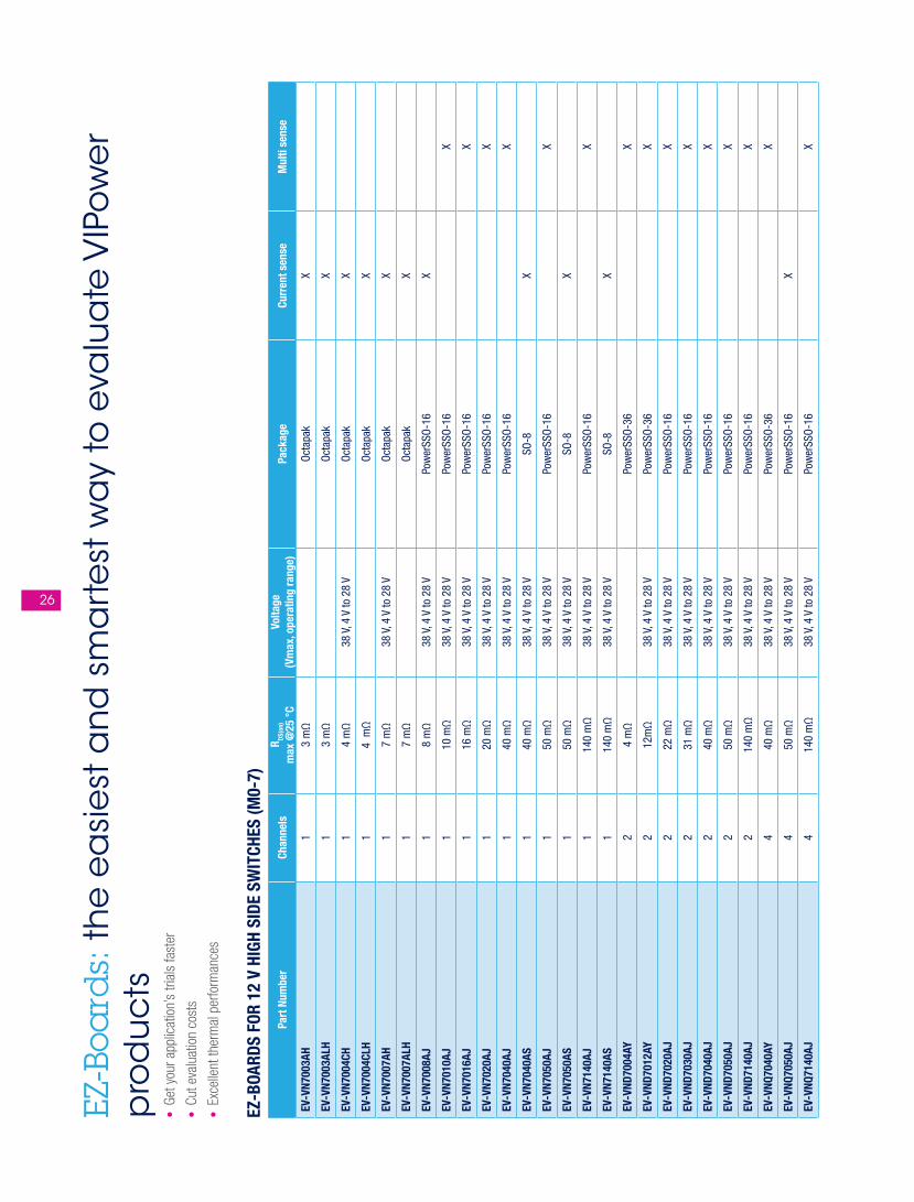
26
EZ-B
oard
s: th
e e
asi
est
an
d s
ma
rte
st w
ay
to e
valu
ate
VIP
ow
er
pro
du
cts
• Ge
t you
r app
licat
ion’
s tri
als
fast
er
• Cu
t eva
luat
ion
cost
s
• Ex
celle
nt th
erm
al p
erfo
rman
ces
EZ-B
OARD
S FO
R 12
V H
IGH
SIDE
SW
ITCH
ES (M
0-7)
Part
Num
ber
Chan
nels
R DS(o
n)
max
@25
°C
Volta
ge(V
max
, ope
ratin
g ra
nge)
Pack
age
Curr
ent s
ense
Mul
ti se
nse
EV-V
N700
3AH
13
mΩ
Octa
pak
X
EV-V
N700
3ALH
13
mΩ
Octa
pak
X
EV-V
N700
4CH
14
mΩ
38 V
, 4 V
to 2
8 V
Octa
pak
X
EV-V
N700
4CLH
14
mΩ
Octa
pak
X
EV-V
N700
7AH
17
mΩ
38 V
, 4 V
to 2
8 V
Octa
pak
X
EV-V
N700
7ALH
17
mΩ
Octa
pak
X
EV-V
N700
8AJ
18
mΩ
38 V
, 4 V
to 2
8 V
Pow
erSS
O‑16
X
EV-V
N701
0AJ
110
mΩ
38 V
, 4 V
to 2
8 V
Pow
erSS
O‑16
X
EV-V
N701
6AJ
116
mΩ
38 V
, 4 V
to 2
8 V
Pow
erSS
O‑16
X
EV-V
N702
0AJ
120
mΩ
38 V
, 4 V
to 2
8 V
Pow
erSS
O‑16
X
EV-V
N704
0AJ
140
mΩ
38 V
, 4 V
to 2
8 V
Pow
erSS
O‑16
X
EV-V
N704
0AS
140
mΩ
38 V
, 4 V
to 2
8 V
SO‑8
X
EV-V
N705
0AJ
150
mΩ
38 V
, 4 V
to 2
8 V
Pow
erSS
O‑16
X
EV-V
N705
0AS
150
mΩ
38 V
, 4 V
to 2
8 V
SO‑8
X
EV-V
N714
0AJ
114
0 m
Ω38
V, 4
V to
28
VPo
wer
SSO‑
16X
EV-V
N714
0AS
114
0 m
Ω38
V, 4
V to
28
VSO
‑8X
EV-V
ND70
04AY
24
mΩ
Pow
erSS
O‑36
X
EV-V
ND70
12AY
212
mΩ
38 V
, 4 V
to 2
8 V
Pow
erSS
O‑36
X
EV-V
ND70
20AJ
222
mΩ
38 V
, 4 V
to 2
8 V
Pow
erSS
O‑16
X
EV-V
ND70
30AJ
231
mΩ
38 V
, 4 V
to 2
8 V
Pow
erSS
O‑16
X
EV-V
ND70
40AJ
2
40 m
Ω38
V, 4
V to
28
VPo
wer
SSO‑
16X
EV-V
ND70
50AJ
250
mΩ
38 V
, 4 V
to 2
8 V
Pow
erSS
O‑16
X
EV-V
ND71
40AJ
214
0 m
Ω38
V, 4
V to
28
VPo
wer
SSO‑
16X
EV-V
NQ70
40AY
4
40 m
Ω38
V, 4
V to
28
VPo
wer
SSO‑
36X
EV-V
NQ70
50AJ
450
mΩ
38 V
, 4 V
to 2
8 V
Pow
erSS
O‑16
X
EV-V
NQ71
40AJ
414
0 m
Ω38
V, 4
V to
28
VPo
wer
SSO‑
16X
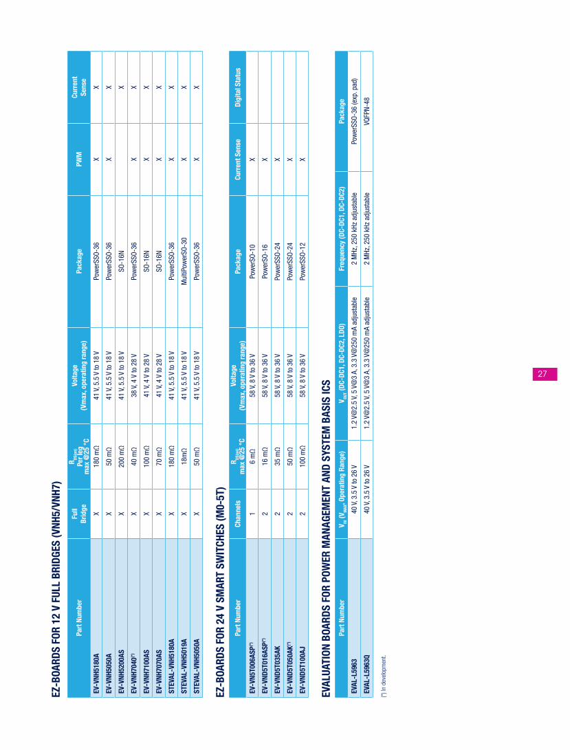
27
EZ-B
OARD
S FO
R 12
V F
ULL
BRID
GES
(VNH
5/VN
H7)
Part
Num
ber
Full
Brid
ge
R DS(o
n)Pe
r leg
max
@25
°C
Volta
ge(V
max
, ope
ratin
g ra
nge)
Pack
age
PWM
Curr
ent
Sens
e
EV-V
NH51
80A
X18
0 m
Ω41
V, 5
.5 V
to 1
8 V
Pow
erSS
O‑36
XX
EV-V
NH50
50A
X50
mΩ
41 V
, 5.5
V to
18
VPo
wer
SSO‑
36X
X
EV-V
NH52
00AS
X20
0 m
Ω41
V, 5
.5 V
to 1
8 V
SO‑1
6NX
EV-V
NH70
40(*
)X
40 m
Ω38
V, 4
V to
28
VPo
wer
SSO‑
36X
X
EV-V
NH71
00AS
X10
0 m
Ω41
V, 4
V to
28
VSO
‑16N
XX
EV-V
NH70
70AS
X70
mΩ
41 V
, 4 V
to 2
8 V
SO‑1
6NX
X
STEV
AL-V
NH51
80A
X18
0 m
Ω41
V, 5
.5 V
to 1
8 V
Pow
erSS
O‑36
XX
STEV
AL-V
NH50
19A
X18
mΩ
41 V
, 5.5
V to
18
VM
ultiP
ower
SO‑3
0X
X
STEV
AL-V
NH50
50A
X50
mΩ
41 V
, 5.5
V to
18
VPo
wer
SSO‑
36X
X
EZ-B
OARD
S FO
R 24
V S
MAR
T SW
ITCH
ES (M
0-5T
)
Part
Num
ber
Chan
nels
R DS(o
n)m
ax @
25 °
C Vo
ltage
(Vm
ax, o
pera
ting
rang
e)Pa
ckag
eCu
rren
t Sen
seDi
gita
l Sta
tus
EV-V
N5T0
06AS
P(*)
16
mΩ
58 V
, 8 V
to 3
6 V
Pow
erSO
‑10
X
EV-V
ND5T
016A
SP(*
)2
16 m
Ω58
V, 8
V to
36
VPo
wer
SO‑1
6X
EV-V
ND5T
035A
K2
35 m
Ω58
V, 8
V to
36
VPo
wer
SSO‑
24X
EV-V
ND5T
050A
K(*)
250
mΩ
58 V
, 8 V
to 3
6 V
Pow
erSS
O‑24
X
EV-V
ND5T
100A
J2
100
mΩ
58 V
, 8 V
to 3
6 V
Pow
erSS
O‑12
X
EVAL
UATI
ON B
OARD
S FO
R PO
WER
MAN
AGEM
ENT
AND
SYST
EM B
ASIS
ICS
Part
Num
ber
V IN (V
MAX
, Ope
ratin
g Ra
nge)
V OUT (
DC-D
C1, D
C-DC
2, L
DO)
Freq
uenc
y (D
C-DC
1, D
C-DC
2)Pa
ckag
e
EVAL
-L59
6340
V, 3
.5 V
to 2
6 V
1.2
V@2.
5 V,
5 V
@3
A, 3
.3 V
@25
0 m
A ad
just
able
2 M
Hz, 2
50 k
Hz a
djus
tabl
ePo
wer
SSO‑
36 (e
xp. p
ad)
EVAL
-L59
63Q
40 V
, 3.5
V to
26
V1.
2 V@
2.5
V, 5
V@
3 A,
3.3
V@
250
mA
adju
stab
le2
MHz
, 250
kHz
adj
usta
ble
VQFP
N‑48
(*) In
dev
elop
men
t.

© STMicroelectronics - February 2017 - Printed in United Kingdom - All rights reservedThe STMicroelectronics corporate logo is a registered trademark of the STMicroelectronics group of companies
All other names are the property of their respective owners
For more information on ST products and solutions, visit www.st.comOrder code: A4SGCAR0217


![MICRO SWITCH™ Compact Limit Switches, NGC Series · 4 sensing.honeywell.com MICRO SWITC Compact Limit Switches NGC Series Figure 3. Side Rotary A1A/A1B Dimensions Side Exit 12 [0.47]](https://img.pdfslide.net/doc/110x75/612a1d738f4a40428a55bbfd/micro-switcha-compact-limit-switches-ngc-series-4-sensinghoneywellcom-micro.jpg)