Embed Size (px)
Citation preview
SMJ320C40, TMP320C40DIGITAL SIGNAL PROCESSORS
SGUS017H -- OCTOBER 1993 -- REVISED OCTOBER 2001
1POST OFFICE BOX 1443 • HOUSTON, TEXAS 77251--1443
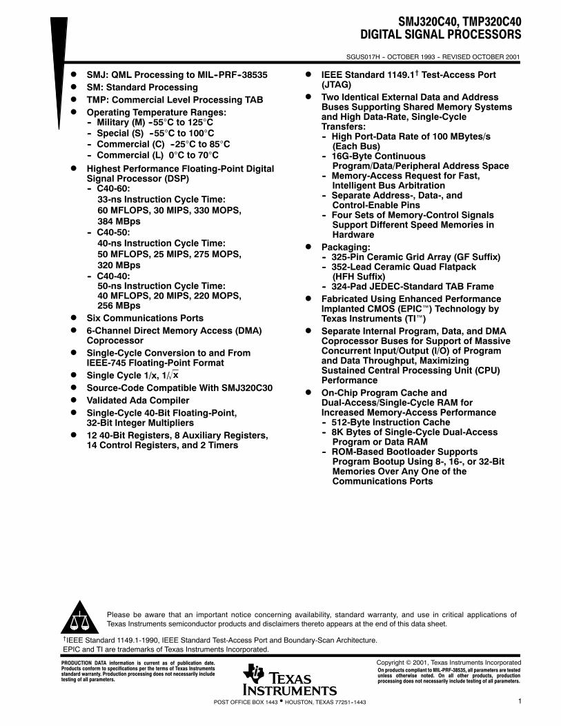
D SMJ: QML Processing to MIL--PRF--38535D SM: Standard ProcessingD TMP: Commercial Level Processing TABD Operating Temperature Ranges:
-- Military (M) --55°C to 125°C-- Special (S) --55°C to 100°C-- Commercial (C) --25°C to 85°C-- Commercial (L) 0°C to 70°C
D Highest Performance Floating-Point DigitalSignal Processor (DSP)-- C40-60:33-ns Instruction Cycle Time:60 MFLOPS, 30 MIPS, 330 MOPS,384 MBps
-- C40-50:40-ns Instruction Cycle Time:50 MFLOPS, 25 MIPS, 275 MOPS,320 MBps
-- C40-40:50-ns Instruction Cycle Time:40 MFLOPS, 20 MIPS, 220 MOPS,256 MBps
D Six Communications PortsD 6-Channel Direct Memory Access (DMA)
CoprocessorD Single-Cycle Conversion to and From
IEEE-745 Floating-Point FormatD Single Cycle 1/x, 1/D Source-Code Compatible With SMJ320C30D Validated Ada CompilerD Single-Cycle 40-Bit Floating-Point,
32-Bit Integer MultipliersD 12 40-Bit Registers, 8 Auxiliary Registers,
14 Control Registers, and 2 Timers
D IEEE Standard 1149.1† Test-Access Port(JTAG)
D Two Identical External Data and AddressBuses Supporting Shared Memory Systemsand High Data-Rate, Single-CycleTransfers:-- High Port-Data Rate of 100 MBytes/s(Each Bus)
-- 16G-Byte ContinuousProgram/Data/Peripheral Address Space
-- Memory-Access Request for Fast,Intelligent Bus Arbitration
-- Separate Address-, Data-, andControl-Enable Pins
-- Four Sets of Memory-Control SignalsSupport Different Speed Memories inHardware
D Packaging:-- 325-Pin Ceramic Grid Array (GF Suffix)-- 352-Lead Ceramic Quad Flatpack(HFH Suffix)
-- 324-Pad JEDEC-Standard TAB FrameD Fabricated Using Enhanced Performance
Implanted CMOS (EPIC™) Technology byTexas Instruments (TI™)
D Separate Internal Program, Data, and DMACoprocessor Buses for Support of MassiveConcurrent Input/Output (I/O) of Programand Data Throughput, MaximizingSustained Central Processing Unit (CPU)Performance
D On-Chip Program Cache andDual-Access/Single-Cycle RAM forIncreased Memory-Access Performance-- 512-Byte Instruction Cache-- 8K Bytes of Single-Cycle Dual-AccessProgram or Data RAM
-- ROM-Based Bootloader SupportsProgram Bootup Using 8-, 16-, or 32-BitMemories Over Any One of theCommunications Ports
Please be aware that an important notice concerning availability, standard warranty, and use in critical applications ofTexas Instruments semiconductor products and disclaimers thereto appears at the end of this data sheet.
PRODUCTION DATA information is current as of publication date.Products conform to specifications per the terms of Texas Instrumentsstandard warranty. Production processing does not necessarily includetesting of all parameters.
Copyright © 2001, Texas Instruments Incorporated
x
†IEEE Standard 1149.1-1990, IEEE Standard Test-Access Port and Boundary-Scan Architecture.EPIC and TI are trademarks of Texas Instruments Incorporated.
On products compliant to MIL-PRF-38535, all parameters are testedunless otherwise noted. On all other products, productionprocessing does not necessarily include testing of all parameters.

SMJ320C40, TMP320C40DIGITAL SIGNAL PROCESSORS
SGUS017H -- OCTOBER 1993 -- REVISED OCTOBER 2001
2 POST OFFICE BOX 1443 • HOUSTON, TEXAS 77251--1443
pinouts
352-LEAD HFH QUAD FLATPACK PACKAGE(TOP VIEW)†
352 265
264
177
17689
88
1
1234567891011 1312
1514 16
17181920212223242526 2827
3029 31
32333435
AB
CD
EF
GH
JK
LM
NP
RT
UV
WY
AAAB
ACAD
AEAF
AGAH
AJAK
ALAM
ANAP
AR
Pin A1
325-PIN GF GRID ARRAY PACKAGE(BOTTOM VIEW)†
1
TAB 325-LEAD OLB/ILBTAPE AUTOMATED BONDING (TAB) PACKAGE
(TOP VIEW)†
† See the pin assignments tables and the signal description table for location and description of all pins.
SMJ320C40, TMP320C40DIGITAL SIGNAL PROCESSORS
SGUS017H -- OCTOBER 1993 -- REVISED OCTOBER 2001
3POST OFFICE BOX 1443 • HOUSTON, TEXAS 77251--1443
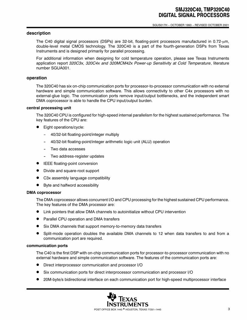
description
The C40 digital signal processors (DSPs) are 32-bit, floating-point processors manufactured in 0.72-μm,double-level metal CMOS technology. The 320C40 is a part of the fourth-generation DSPs from TexasInstruments and is designed primarily for parallel processing.
For additional information when designing for cold temperature operation, please see Texas Instrumentsapplication report 320C3x, 320C4x and 320MCM42x Power-up Sensitivity at Cold Temperature, literaturenumber SGUA001.
operation
The 320C40 has six on-chip communication ports for processor-to-processor communication with no externalhardware and simple communication software. This allows connectivity to other C4x processors with noexternal-glue logic. The communication ports remove input/output bottlenecks, and the independent smartDMA coprocessor is able to handle the CPU input/output burden.
central processing unit
The 320C40 CPU is configured for high-speed internal parallelism for the highest sustained performance. Thekey features of the CPU are:
D Eight operations/cycle:
-- 40/32-bit floating-point/integer multiply
-- 40/32-bit floating-point/integer arithmetic logic unit (ALU) operation
-- Two data accesses
-- Two address-register updates
D IEEE floating-point conversion
D Divide and square-root support
D C3x assembly language compatibility
D Byte and halfword accessibility
DMA coprocessor
TheDMA coprocessor allows concurrent I/O and CPU processing for the highest sustained CPU performance.The key features of the DMA processor are:
D Link pointers that allow DMA channels to autoinitialize without CPU intervention
D Parallel CPU operation and DMA transfers
D Six DMA channels that support memory-to-memory data transfers
D Split-mode operation doubles the available DMA channels to 12 when data transfers to and from acommunication port are required.
communication ports
The C40 is the first DSP with on-chip communication ports for processor-to-processor communication with noexternal hardware and simple communication software. The features of the communication ports are:
D Direct interprocessor communication and processor I/O
D Six communication ports for direct interprocessor communication and processor I/O
D 20M-byte/s bidirectional interface on each communication port for high-speed multiprocessor interface

SMJ320C40, TMP320C40DIGITAL SIGNAL PROCESSORS
SGUS017H -- OCTOBER 1993 -- REVISED OCTOBER 2001
4 POST OFFICE BOX 1443 • HOUSTON, TEXAS 77251--1443
communication ports (continued)
D Separate 8-word-deep input and output FIFO buffers for processor-to-processor communication and I/O
D Automatic arbitration and handshaking for direct processor-to-processor connection
communication-port software reset (C40 silicon revision ≥ 5.0)
The input and output FIFO levels for a communication port can be flushed by writing at least two back-to-backvalues to its communication-port software-reset address as specified in Table 1. This feature is not present inC40 silicon revision < 5.0. This software reset flushes any word or byte already present in the FIFOs but it doesnot affect the status of the communication-port pins. Figure 1 shows an example ofcommunication-port-software reset.
Table 1. Communication-Port Software-Reset Address
0 0x0100043
1 0x0100053
2 0x0100063
3 0x0100073
4 0x0100083
5 0x0100093
; -------------------------------------------------;; RESET1:Flush’s FIFO data for communication port 1;; -------------------------------------------------;RESET1 push AR0 ; Save registers
push R0 ;push RC ;ldhi 010h,AR0 ; Set AR0 to base address of COM 1or 050h,AR0 ;
flush: rpts 1 ; Flush FIFO data with back-to-back writesti R0,*+AR0(3) ;rpts 10 ; Waitnop ;ldi *+AR0(0),R0 ; Check for new data from other portand 01FE0h,R0 ;bnz flush ;pop RC ; Restore registerspop R0 ;pop AR0 ;rets ; Return
Figure 1. Example of Communication-Port-Software Reset

SMJ320C40, TMP320C40DIGITAL SIGNAL PROCESSORS
SGUS017H -- OCTOBER 1993 -- REVISED OCTOBER 2001
5POST OFFICE BOX 1443 • HOUSTON, TEXAS 77251--1443
NMI with bus-grant feature (C40 silicon revision ≥ 5.0)
The320C40devices have a software-configurable feature that forces the internal-peripheral bus to readywhenthe NMI signal is asserted. This feature is not present in C40 silicon revision < 5.0. The NMI bus-grant featureis enabled when bits 19--18 of the status register (ST) are set to 10b. When enabled, a peripheral bus-grantsignal is generated on the falling edge of NMI. When NMI is asserted and this feature is not enabled, the CPUstalls on access to the peripheral bus if it is not ready. A stall condition occurs when writing to a full FIFO orreading an empty FIFO. This feature is useful in correcting communication-port errorswhenused in conjunctionwith the communication-port software-reset feature.
IDLE2 clock-stop power-down mode (C40 silicon revision ≥ 5.0)
The 320C40 has a clock-stop mode or power-down mode (IDLE2) to achieve extremely low powerconsumption. When an IDLE2 instruction is executed, the clocks are halted with H1 being held high. To exitIDLE2, assert one of the IIOF3--IIOF0 pins configured as an external interrupt instead of a general-purpose I/O.A macro showing how to generate the IDLE2 opcode is given in Figure 2. During this power-down mode:
D No instructions are executed
D The CPU, peripherals, and internal memory retain their previous state.
D The external-bus outputs are idle. The address lines remain in their previous state, the data lines are inthe high-impedance state, and the output-control signals are inactive.
; ------------------------------------------------;; IDLE2: Macro to generate idle2 opcode ;; ------------------------------------------------;IDLE2 .macro
.word 06000001h
.endm
Figure 2. Example of Software Subroutine Using IDLE2
IDLE2 is exited when one of the five external interrupts (NMI and IIOF3--IIOF0) is asserted low for at least fourinput clocks (two H1 cycles). The clocks then start after a delay of two input clocks (one H1 cycle). The clockscan start in the opposite phase; that is, H1 can be high when H3 was high before the clocks were stopped.However, the H1 and H3 clocks remain 180° out of phase with each other.
During IDLE2 operation, an external interrupt can be recognized and serviced by the CPU if it is enabled beforeentering IDLE2 and asserted for at least two H1 cycles. For the processor to recognize only one interrupt, theinterrupt pin must be configured for edge-trigger mode or asserted less than three cycles in level-trigger mode.Any external interrupt pin canwake up the device from IDLE2, but for theCPU to recognize that interrupt, itmustalso be enabled. If an interrupt is recognized and executed by the CPU, the instruction following the IDLE2instruction is not executed until after execution of a return opcode.
When the device is in emulationmode, the CPU executes an IDLE2 instruction as if it were an IDLE instruction.The clocks continue to run for correct operation of the emulator.
SMJ320C40, TMP320C40DIGITAL SIGNAL PROCESSORS
SGUS017H -- OCTOBER 1993 -- REVISED OCTOBER 2001
6 POST OFFICE BOX 1443 • HOUSTON, TEXAS 77251--1443
development tools
The C40 is supported by a host of parallel-processing development tools for developing and simulating codeeasily and for debugging parallel-processing systems. The code generation tools include:
D An ANSI C compiler optimized with a runtime support library that supports use of communication ports andDMA.
D Third-party support for C, C++, and Ada compilers
D Several operating systems available for parallel-processing support, as well as DMA and communicationport drivers
D An assembler and linker with support for mapping program and data to parallel processors
The simulation tools include:
D Parallel DSPsystem-level simulationwith LAI hardware verification (HV)model and full function (FF)model
D TI software simulator with high-level language debugger interface for simulating a single processor
The hardware development and verification tools include:
D Parallel processor in-circuit emulator and high-level language debugger: XDS510™
D Parallel processor development system (PPDS) with four 320C40s, local and global memory, andcommunication port connections
XDS510 is a trademark of Texas Instruments Incorporated.
SMJ320C40, TMP320C40DIGITAL SIGNAL PROCESSORS
SGUS017H -- OCTOBER 1993 -- REVISED OCTOBER 2001
7POST OFFICE BOX 1443 • HOUSTON, TEXAS 77251--1443
block diagram
Cache(512 Bytes)
32 32
PDATA Bus
DDATA Bus
DADDR 1 Bus
DADDR 2 Bus
DMADATA Bus
RAM Block 0(4K Bytes)
32 32
RAM Block 1(4K Bytes)
32 32
ROM Block(Reserved)
32 32
PADDR Bus
DMAADDR Bus
MUX
D31--D0A30--A0
DEAE
STAT3--STAT0LOCK
STRB0,STRB1R/W0,RW1
PAGE0,PAGE1RDY0,RDY1
CE0,CE1
IR
PC
X1X2/CLKIN
ROMENRESET
RESETLOC0,RESETLOC1
NMIIIOF3--IIOF0
IACKH1
H3CVSSDVDDDVSSIVSS
LADVDDLDDVDD
VDDLVSSLSUBS
32
Controller
3232 32
40 40
40
40
32-Bit BarrelShifter
40
40ALU
ExtendedPrecisionRegisters(R0--R11)
40
40
32 40
40
DISP, IR0, IR1
ARAU0 ARAU1BK
AuxiliaryRegisters(AR0--AR7)
OtherRegisters
(14)
CPU1
CPU2
32
3232
32
3232
32
3232
32
REG1
32
MUX
CPU1
REG1
Multiplier
Continued
onnextpage
REG2REG2
REG 1
REG1

SMJ320C40, TMP320C40DIGITAL SIGNAL PROCESSORS
SGUS017H -- OCTOBER 1993 -- REVISED OCTOBER 2001
8 POST OFFICE BOX 1443 • HOUSTON, TEXAS 77251--1443
block diagram (continued)
LD31--LD0LA30--LA0LDELAELSTAT3--LSTAT0LLOCKLSTRB0--LSTRB1LR/W0--LR/W1LPAGE0--LPAGE1LRDY0--LRDY1LCE0, LCE1
DMA Channel 0DMA Channel 1DMA Channel 2DMA Channel 3DMA Channel 4DMA Channel 5
DMA Coprocessor
Six DMA Channels
3232
GlobalLocal
Port Control
Global Control RegisterTime Period Register
Timer 1
Timer Counter Register
TCLK1
Global Control RegisterTime Period Register
Timer 0
Timer Counter Register
TCLK0
Port Control Registers
OutputFIFO
InputFIFO
PAU
COM Port 0CREQ0CACK0CSTRB0CRDY0C0D7--C0D0
Peripheral
Data
Bus
Peripheral
Address
Bus
Continued
frompreviouspage
Port Control Registers
OutputFIFO
InputFIFO
PAU
COM Port 5CREQ5CACK5CSTRB5CRDY5C5D7--C5D0
MUX
DDATA Bus
DADDR 1 Bus
DADDR 2 Bus
DMADATA Bus
PADDR Bus
DMAADDR Bus
PDATA Bus
MUX
SixCommunicationPorts32
32
32
32
32
32
32
32
32
32
32
32
32
32
32
32
SMJ320C40, TMP320C40DIGITAL SIGNAL PROCESSORS
SGUS017H -- OCTOBER 1993 -- REVISED OCTOBER 2001
9POST OFFICE BOX 1443 • HOUSTON, TEXAS 77251--1443
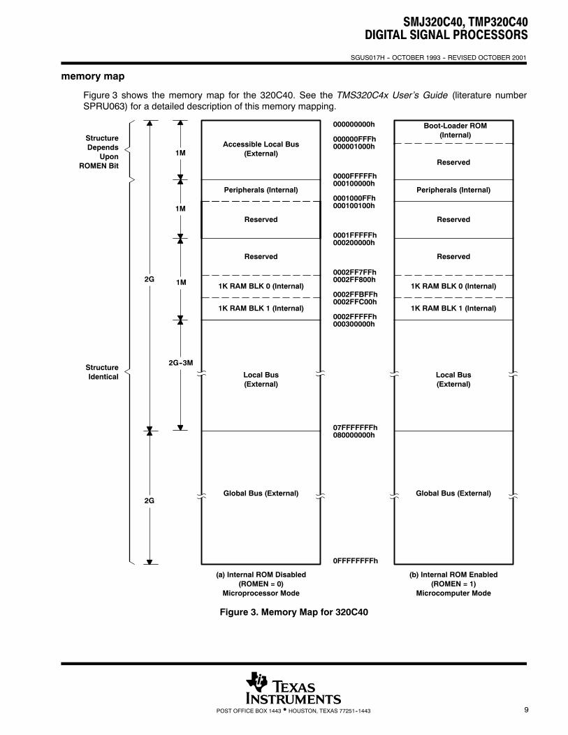
memory map
Figure 3 shows the memory map for the 320C40. See the TMS320C4x User’s Guide (literature numberSPRU063) for a detailed description of this memory mapping.
000000000h
000000FFFh000001000h
0000FFFFFh000100000h
0001000FFh000100100h
0001FFFFFh000200000h
0002FF7FFh0002FF800h
0002FFBFFh0002FFC00h
0002FFFFFh000300000h
07FFFFFFFh080000000h
0FFFFFFFFh
Accessible Local Bus(External)
Peripherals (Internal)
Reserved
Reserved
1K RAM BLK 0 (Internal)
1K RAM BLK 1 (Internal)
Local Bus(External)
Global Bus (External)
(a) Internal ROM Disabled(ROMEN = 0)
Microprocessor Mode
Boot-Loader ROM(Internal)
Peripherals (Internal)
Reserved
Reserved
1K RAM BLK 0 (Internal)
1K RAM BLK 1 (Internal)
Local Bus(External)
Global Bus (External)
(b) Internal ROM Enabled(ROMEN = 1)
Microcomputer Mode
1M
1M
1M
2G--3M
StructureDepends
UponROMEN Bit
StructureIdentical
2G
2G
Reserved
Figure 3. Memory Map for 320C40

SMJ320C40, TMP320C40DIGITAL SIGNAL PROCESSORS
SGUS017H -- OCTOBER 1993 -- REVISED OCTOBER 2001
10 POST OFFICE BOX 1443 • HOUSTON, TEXAS 77251--1443
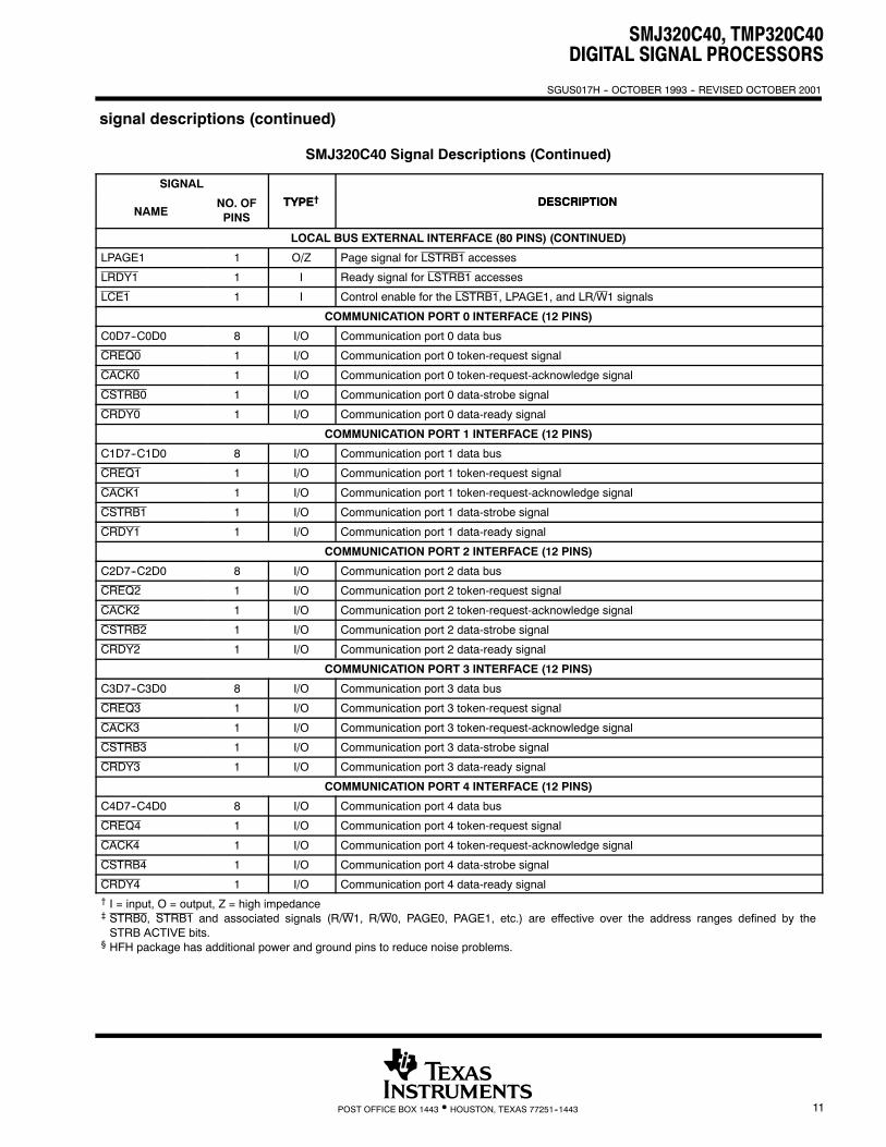
signal descriptions
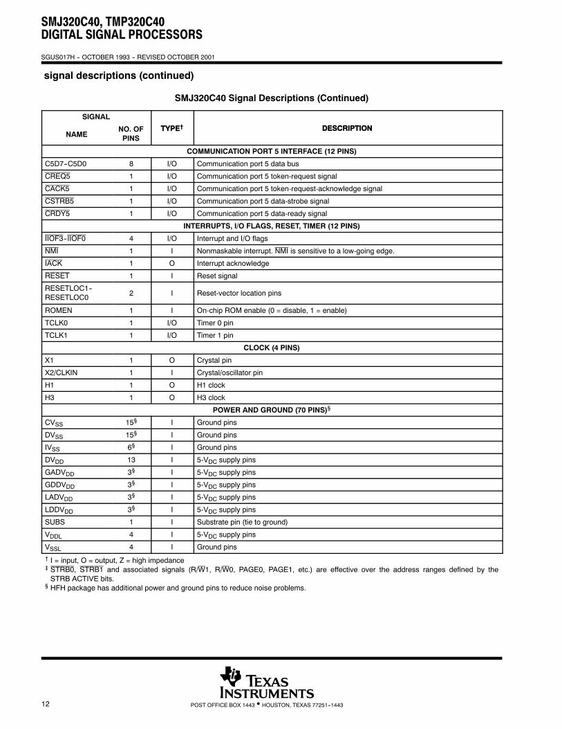
This section gives signal descriptions for the SMJ320C40 device. The SMJ320C40 signal descriptions tablelists each signal, the number of pins, operating mode(s) (that is, input, output, or high-impedance state asindicated by I, O, or Z, respectively), and function. All pins labeled NC are not to be connected by the user. Aline over a signal name (for example, RESET) indicates that the signal is active low (true at a logic-0 level). Thesignals are grouped according to functions.
SMJ320C40 Signal Descriptions
SIGNAL
NAMENO. OFPINS
TYPE† DESCRIPTION
GLOBAL BUS EXTERNAL INTERFACE (80 PINS)
D31--D0 32 I/O/Z 32-bit data port of the global bus external interface
DE 1 I Data-bus-enable signal for the global bus external interface
A30--A0 31 O/Z 31-bit address port of the global bus external interface
AE 1 I Address-bus-enable signal for the global bus external interface
STAT3--STAT0 4 O Status signals for the global bus external interface
LOCK 1 O Lock signal for the global bus external interface
STRB0‡ 1 O/Z Access strobe 0 for the global bus external interface
R/W0‡ 1 O/Z Read/write signal for STRB0 accesses
PAGE0‡ 1 O/Z Page signal for STRB0 accesses
RDY0‡ 1 I Ready signal for STRB0 accesses
CE0‡ 1 I Control enable for the STRB0, PAGE0, and R/W0 signals
STRB1‡ 1 O/Z Access strobe 1 for the global bus external interface
R/W1‡ 1 O/Z Read/write signal for STRB1 accesses
PAGE1‡ 1 O/Z Page signal for STRB1 accesses
RDY1‡ 1 I Ready signal for STRB1 accesses
CE1‡ 1 I Control enable for the STRB1, PAGE1, and R/W1 signals
LOCAL BUS EXTERNAL INTERFACE (80 PINS)
LD31--LD0 32 I/O/Z 32-bit data port of the local bus external interface
LDE 1 I Data-bus-enable signal for the local bus external interface
LA30--LA0 31 O/Z 31-bit address port of the local bus external interface
LAE 1 I Address-bus-enable signal for the local bus external interface
LSTAT3--LSTAT0 4 O Status signals for the local bus external interface
LLOCK 1 O Lock signal for the local bus external interface
LSTRB0‡ 1 O/Z Access strobe 0 for the local bus external interface
LR/W0 1 O/Z Read/write signal for LSTRB0 accesses
LPAGE0 1 O/Z Page signal for LSTRB0 accesses
LRDY0 1 I Ready signal for LSTRB0 accesses
LCE0 1 I Control enable for the LSTRB0, LPAGE0, and LR/W0 signals
LSTRB1‡ 1 O/Z Access strobe 1 for the local bus external interface
LR/W1 1 O/Z Read/write signal for LSTRB1 accesses† I = input, O = output, Z = high impedance‡ STRB0, STRB1 and associated signals (R/W1, R/W0, PAGE0, PAGE1, etc.) are effective over the address ranges defined by theSTRB ACTIVE bits.
§ HFH package has additional power and ground pins to reduce noise problems.
SMJ320C40, TMP320C40DIGITAL SIGNAL PROCESSORS
SGUS017H -- OCTOBER 1993 -- REVISED OCTOBER 2001
11POST OFFICE BOX 1443 • HOUSTON, TEXAS 77251--1443
SMJ320C40 Signal Descriptions (Continued)
SIGNAL
DESCRIPTIONTYPE†NAME
DESCRIPTIONTYPE†NO. OFPINS
LOCAL BUS EXTERNAL INTERFACE (80 PINS) (CONTINUED)
LPAGE1 1 O/Z Page signal for LSTRB1 accesses
LRDY1 1 I Ready signal for LSTRB1 accesses
LCE1 1 I Control enable for the LSTRB1, LPAGE1, and LR/W1 signals
COMMUNICATION PORT 0 INTERFACE (12 PINS)
C0D7--C0D0 8 I/O Communication port 0 data bus
CREQ0 1 I/O Communication port 0 token-request signal
CACK0 1 I/O Communication port 0 token-request-acknowledge signal
CSTRB0 1 I/O Communication port 0 data-strobe signal
CRDY0 1 I/O Communication port 0 data-ready signal
COMMUNICATION PORT 1 INTERFACE (12 PINS)
C1D7--C1D0 8 I/O Communication port 1 data bus
CREQ1 1 I/O Communication port 1 token-request signal
CACK1 1 I/O Communication port 1 token-request-acknowledge signal
CSTRB1 1 I/O Communication port 1 data-strobe signal
CRDY1 1 I/O Communication port 1 data-ready signal
COMMUNICATION PORT 2 INTERFACE (12 PINS)
C2D7--C2D0 8 I/O Communication port 2 data bus
CREQ2 1 I/O Communication port 2 token-request signal
CACK2 1 I/O Communication port 2 token-request-acknowledge signal
CSTRB2 1 I/O Communication port 2 data-strobe signal
CRDY2 1 I/O Communication port 2 data-ready signal
COMMUNICATION PORT 3 INTERFACE (12 PINS)
C3D7--C3D0 8 I/O Communication port 3 data bus
CREQ3 1 I/O Communication port 3 token-request signal
CACK3 1 I/O Communication port 3 token-request-acknowledge signal
CSTRB3 1 I/O Communication port 3 data-strobe signal
CRDY3 1 I/O Communication port 3 data-ready signal
COMMUNICATION PORT 4 INTERFACE (12 PINS)
C4D7--C4D0 8 I/O Communication port 4 data bus
CREQ4 1 I/O Communication port 4 token-request signal
CACK4 1 I/O Communication port 4 token-request-acknowledge signal
CSTRB4 1 I/O Communication port 4 data-strobe signal
CRDY4 1 I/O Communication port 4 data-ready signal† I = input, O = output, Z = high impedance‡ STRB0, STRB1 and associated signals (R/W1, R/W0, PAGE0, PAGE1, etc.) are effective over the address ranges defined by theSTRB ACTIVE bits.
§ HFH package has additional power and ground pins to reduce noise problems.
signal descriptions (continued)
SMJ320C40, TMP320C40DIGITAL SIGNAL PROCESSORS
SGUS017H -- OCTOBER 1993 -- REVISED OCTOBER 2001
12 POST OFFICE BOX 1443 • HOUSTON, TEXAS 77251--1443
SMJ320C40 Signal Descriptions (Continued)
SIGNAL
DESCRIPTIONTYPE†NAME
DESCRIPTIONTYPE†NO. OFPINS
COMMUNICATION PORT 5 INTERFACE (12 PINS)
C5D7--C5D0 8 I/O Communication port 5 data bus
CREQ5 1 I/O Communication port 5 token-request signal
CACK5 1 I/O Communication port 5 token-request-acknowledge signal
CSTRB5 1 I/O Communication port 5 data-strobe signal
CRDY5 1 I/O Communication port 5 data-ready signal
INTERRUPTS, I/O FLAGS, RESET, TIMER (12 PINS)
IIOF3--IIOF0 4 I/O Interrupt and I/O flags
NMI 1 I Nonmaskable interrupt. NMI is sensitive to a low-going edge.
IACK 1 O Interrupt acknowledge
RESET 1 I Reset signal
RESETLOC1--RESETLOC0
2 I Reset-vector location pins
ROMEN 1 I On-chip ROM enable (0 = disable, 1 = enable)
TCLK0 1 I/O Timer 0 pin
TCLK1 1 I/O Timer 1 pin
CLOCK (4 PINS)
X1 1 O Crystal pin
X2/CLKIN 1 I Crystal/oscillator pin
H1 1 O H1 clock
H3 1 O H3 clock
POWER AND GROUND (70 PINS)§
CVSS 15§ I Ground pins
DVSS 15§ I Ground pins
IVSS 6§ I Ground pins
DVDD 13 I 5-VDC supply pins
GADVDD 3§ I 5-VDC supply pins
GDDVDD 3§ I 5-VDC supply pins
LADVDD 3§ I 5-VDC supply pins
LDDVDD 3§ I 5-VDC supply pins
SUBS 1 I Substrate pin (tie to ground)
VDDL 4 I 5-VDC supply pins
VSSL 4 I Ground pins
† I = input, O = output, Z = high impedance‡ STRB0, STRB1 and associated signals (R/W1, R/W0, PAGE0, PAGE1, etc.) are effective over the address ranges defined by theSTRB ACTIVE bits.
§ HFH package has additional power and ground pins to reduce noise problems.
signal descriptions (continued)

SMJ320C40, TMP320C40DIGITAL SIGNAL PROCESSORS
SGUS017H -- OCTOBER 1993 -- REVISED OCTOBER 2001
13POST OFFICE BOX 1443 • HOUSTON, TEXAS 77251--1443
SMJ320C40 Signal Descriptions (Continued)
SIGNAL
DESCRIPTIONTYPE†NAME
DESCRIPTIONTYPE†NO. OFPINS
EMULATION (7 PINS)
TCK 1 I IEEE 1149.1 test port clock
TDO 1 O/Z IEEE 1149.1 test port data out
TDI 1 I IEEE 1149.1 test port data in
TMS 1 I IEEE 1149.1 test port mode select
TRST 1 I IEEE 1149.1 test port reset
EMU0 1 I/O Emulation pin 0
EMU1 1 I/O Emulation pin 1† I = input, O = output, Z = high impedance‡ STRB0, STRB1 and associated signals (R/W1, R/W0, PAGE0, PAGE1, etc.) are effective over the address ranges defined by theSTRB ACTIVE bits.
§ HFH package has additional power and ground pins to reduce noise problems.
signal descriptions (continued)

SMJ320C40, TMP320C40DIGITAL SIGNAL PROCESSORS
SGUS017H -- OCTOBER 1993 -- REVISED OCTOBER 2001
14 POST OFFICE BOX 1443 • HOUSTON, TEXAS 77251--1443
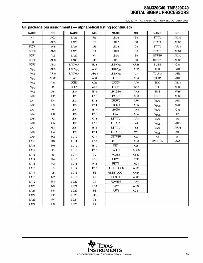
GF package pin assignments — alphabetical listing
NAME NO. NAME NO. NAME NO. NAME NO. NAME NO.
A0 D32 C0D6 AN7 C5D4 AM30 CVSS E35 D31 F32
A1 B32 C0D7 AK8 C5D5 AP32 CVSS AR25 DE AA31
A2 D30 C1D0 AL7 C5D6 AM32 CVSS AE1 DVDD AR11
A3 C29 C1D1 AP8 C5D7 AL31 CVSS AR13 DVDD AR29
A4 B30 C1D2 AM8 CACK0 AN11 CVSS A19 DVDD A13
A5 F28 C1D3 AK12 CACK1 AN13 CVSS R35 DVDD A7
A6 F24 C1D4 AK10 CACK2 AM14 CVSS AL1 DVDD A17
A7 E29 C1D5 AN9 CACK3 AM16 D0 U33 DVDD L35
A8 C27 C1D6 AL9 CACK4 AK32 D1 V32 DVDD AR23
A9 D28 C1D7 AP10 CACK5 AJ31 D2 T34 DVDD A29
A10 B28 C2D0 AM18 CE0 AA33 D3 U31 DVDD L1
A11 F26 C2D1 AN19 CE1 V34 D4 R33 DVDD AC1
A12 C25 C2D2 AL19 CRDY0 AP12 D5 P34 DVDD AR17
A13 E27 C2D3 AP20 CRDY1 AP14 D6 T32 DVDD A23
A14 B26 C2D4 AM20 CRDY2 AL15 D7 N33 DVDD AJ1
A15 D26 C2D5 AN21 CRDY3 AL17 D8 R31 DVSS AJ35
A16 C23 C2D6 AL21 CRDY4 AH30 D9 M34 DVSS A21
A17 B24 C2D7 AP22 CRDY5 AH32 D10 P32 DVSS A25
A18 E25 C3D0 AM22 CREQ0 AM10 D11 L33 DVSS G35
A19 C21 C3D1 AN23 CREQ1 AM12 D12 N31 DVSS A11
A20 D24 C3D2 AL23 CREQ2 AN15 D13 K34 DVSS AG1
A21 B22 C3D3 AP24 CREQ3 AN17 D14 M32 DVSS AM2
A22 E23 C3D4 AM24 CREQ4 AN33 D15 J33 DVSS R1
A23 C19 C3D5 AN25 CREQ5 AL33 D16 L31 DVSS AR21
A24 D22 C3D6 AL25 CSTRB0 AL11 D17 M30 DVSS AR15
A25 B20 C3D7 AP26 CSTRB1 AL13 D18 K32 DVSS A15
A26 E21 C4D0 AN27 CSTRB2 AP16 D19 H34 DVSS AR27
A27 B18 C4D1 AM26 CSTRB3 AP18 D20 J31 DVSS G1
A28 C17 C4D2 AK24 CSTRB4 AM34 D21 G33 DVSS N35
A29 D20 C4D3 AL27 CSTRB5 AK34 D22 K30 DVSS AR9
A30 B16 C4D4 AP28 CVSS AR19 D23 F34 EMU0 AA35
AE AG31 C4D5 AK26 CVSS AR7 D24 H32 EMU1 AD34
C0D0 AP4 C4D6 AN29 CVSS N1 D25 E33 GADVDD B2
C0D1 AL5 C4D7 AM28 CVSS AL35 D26 D34 GADVDD AR1
C0D2 AN5 C5D0 AL29 CVSS A27 D27 G31 GADVDD U35
C0D3 AM4 C5D1 AP30 CVSS A9 D28 C33 GDDVDD V2
C0D4 AP6 C5D2 AK28 CVSS E1 D29 H30 GDDVDD A35
C0D5 AM6 C5D3 AN31 CVSS J35 D30 E31 GDDVDD A1
SMJ320C40, TMP320C40DIGITAL SIGNAL PROCESSORS
SGUS017H -- OCTOBER 1993 -- REVISED OCTOBER 2001
15POST OFFICE BOX 1443 • HOUSTON, TEXAS 77251--1443
GF package pin assignments — alphabetical listing (continued)
NAME NO. NAME NO. NAME NO. NAME NO.
H1 AC3 LA25 R5 LD26 B4 STAT0 AD32
H3 AC5 LA26 T2 LD27 F8 STAT1 AE33
IACK W3 LA27 U3 LD28 D6 STAT2 AF34
IIOF0 AN3 LA28 T4 LD29 C3 STAT3 AE31
IIOF1 AL3 LA29 V4 LD30 E5 STRB0 AD30
IIOF2 AH6 LA30 U5 LD31 F6 STRB1 AC33
IIOF3 AK2 LADVDD B34 LDDVDD AR35 SUBS C31
IVSS AR5 LADVDD AB2 LDDVDD AP2 TCK Y34
IVSS AR31 LADVDD AP34 LDDVDD U1 TCLK0 AE3
IVSS AG35 LAE AB4 LDE AD4 TCLK1 AD2
IVSS A31 LCE0 AG5 LLOCK AA5 TDO AB34
IVSS J1 LCE1 AF2 LOCK W33 TDI AC35
IVSS A5 LD0 E19 LPAGE0 AH2 TMS W35
LA0 D2 LD1 C15 LPAGE1 AG3 TRST AE35
LA1 D4 LD2 D18 LRDY0 AF6 VDDL AN1
LA2 E3 LD3 B14 LRDY1 AE5 VDDL AN35
LA3 F4 LD4 E17 LR/W0 AH4 VDDL C35
LA4 H6 LD5 D16 LR/W1 AF4 VDDL C1
LA5 F2 LD6 C13 LSTAT0 AA3 VSSL A3
LA6 G5 LD7 E15 LSTAT1 Y4 VSSL AR3
LA7 G3 LD8 B12 LSTAT2 Y2 VSSL AR33
LA8 H4 LD9 D14 LSTAT3 W5 VSSL A33
LA9 H2 LD10 C11 LSTRB0 AJ3 X1 W1
LA10 K6 LD11 E13 LSTRB1 AD6 X2/CLKIN AA1
LA11 M6 LD12 B10 NMI AJ5
LA12 J5 LD13 D12 PAGE0 AG33
LA13 J3 LD14 C9 PAGE1 AB32
LA14 K4 LD15 E11 RDY0 Y32
LA15 K2 LD16 F12 RDY1 W31
LA16 L3 LD17 D10 RESETLOC0 AF30
LA17 L5 LD18 B8 RESETLOC1 AH34
LA18 M2 LD19 E9 RESET AJ33
LA19 M4 LD20 C7 ROMEN AK4
LA20 N3 LD21 F10 R/W0 AF32
LA21 N5 LD22 B6 R/W1 AC31
LA22 P2 LD23 D8
LA23 P4 LD24 C5
LA24 R3 LD25 E7

SMJ320C40, TMP320C40DIGITAL SIGNAL PROCESSORS
SGUS017H -- OCTOBER 1993 -- REVISED OCTOBER 2001
16 POST OFFICE BOX 1443 • HOUSTON, TEXAS 77251--1443
GF package pin assignments — numerical listing
NO. NAME NO. NAME NO. NAME NO. NAME
A1 GDDVDD AD30 STRB0 AK24 C4D2 AM30 C5D4
A3 VSSL AD32 STAT0 AK26 C4D5 AM32 C5D6
A5 IVSS AD34 EMU1 AK28 C5D2 AM34 CSTRB4
A7 DVDD AE1 CVSS AK32 CACK4 AN1 VDDL
A9 CVSS AE3 TCLK0 AK34 CSTRB5 AN3 IIOF0
A11 DVSS AE5 LRDY1 AL1 CVSS AN5 C0D2
A13 DVDD AE31 STAT3 AL3 IIOF1 AN7 C0D6
A15 DVSS AE33 STAT1 AL5 C0D1 AN9 C1D5
A17 DVDD AE35 TRST AL7 C1D0 AN11 CACK0
A19 CVSS AF2 LCE1 AL9 C1D6 AN13 CACK1
A21 DVSS AF4 LR/W1 AL11 CSTRB0 AN15 CREQ2
A23 DVDD AF6 LRDY0 AL13 CSTRB1 AN17 CREQ3
A25 DVSS AF30 RESETLOC0 AL15 CRDY2 AN19 C2D1
A27 CVSS AF32 R/W0 AL17 CRDY3 AN21 C2D5
A29 DVDD AF34 STAT2 AL19 C2D2 AN23 C3D1
A31 IVSS AG1 DVSS AL21 C2D6 AN25 C3D5
A33 VSSL AG3 LPAGE1 AL23 C3D2 AN27 C4D0
A35 GDDVDD AG5 LCE0 AL25 C3D6 AN29 C4D6
AA1 X2/CLKIN AG31 AE AL27 C4D3 AN31 C5D3
AA3 LSTAT0 AG33 PAGE0 AL29 C5D0 AN33 CREQ4
AA5 LLOCK AG35 IVSS AL31 C5D7 AN35 VDDL
AA31 DE AH2 LPAGE0 AL33 CREQ5 AP2 LDDVDD
AA33 CE0 AH4 LR/W0 AL35 CVSS AP4 C0D0
AA35 EMU0 AH6 IIOF2 AM2 DVSS AP6 C0D4
AB2 LADVDD AH30 CRDY4 AM4 C0D3 AP8 C1D1
AB4 LAE AH32 CRDY5 AM6 C0D5 AP10 C1D7
AB32 PAGE1 AH34 RESETLOC1 AM8 C1D2 AP12 CRDY0
AB34 TDO AJ1 DVDD AM10 CREQ0 AP14 CRDY1
AC1 DVDD AJ3 LSTRB0 AM12 CREQ1 AP16 CSTRB2
AC3 H1 AJ5 NMI AM14 CACK2 AP18 CSTRB3
AC5 H3 AJ31 CACK5 AM16 CACK3 AP20 C2D3
AC31 R/W1 AJ33 RESET AM18 C2D0 AP22 C2D7
AC33 STRB1 AJ35 DVSS AM20 C2D4 AP24 C3D3
AC35 TDI AK2 IIOF3 AM22 C3D0 AP26 C3D7
AD2 TCLK1 AK4 ROMEN AM24 C3D4 AP28 C4D4
AD4 LDE AK8 C0D7 AM26 C4D1 AP30 C5D1
AD6 LSTRB1 AK10 C1D4 AM28 C4D7 AP32 C5D5
AK12 C1D3 AP34 LADVDD

SMJ320C40, TMP320C40DIGITAL SIGNAL PROCESSORS
SGUS017H -- OCTOBER 1993 -- REVISED OCTOBER 2001
17POST OFFICE BOX 1443 • HOUSTON, TEXAS 77251--1443
GF package pin assignments — numerical listing (continued)
NO. NAME NO. NAME NO. NAME NO. NAME NO. NAME
AR1 GADVDD C1 VDDL E1 CVSS H2 LA9 P2 LA22
AR3 VSSL C3 LD29 E3 LA2 H4 LA8 P4 LA23
AR5 IVSS C5 LD24 E5 LD30 H6 LA4 P32 D10
AR7 CVSS C7 LD20 E7 LD25 H30 D29 P34 D5
AR9 DVSS C9 LD14 E9 LD19 H32 D24 R1 DVSS
AR11 DVDD C11 LD10 E11 LD15 H34 D19 R3 LA24
AR13 CVSS C13 LD6 E13 LD11 J1 IVSS R5 LA25
AR15 DVSS C15 LD1 E15 LD7 J3 LA13 R31 D8
AR17 DVDD C17 A28 E17 LD4 J5 LA12 R33 D4
AR19 CVSS C19 A23 E19 LD0 J31 D20 R35 CVSS
AR21 DVSS C21 A19 E21 A26 J33 D15 T2 LA26
AR23 DVDD C23 A16 E23 A22 J35 CVSS T4 LA28
AR25 CVSS C25 A12 E25 A18 K2 LA15 T32 D6
AR27 DVSS C27 A8 E27 A13 K4 LA14 T34 D2
AR29 DVDD C29 A3 E29 A7 K6 LA10 U1 LDDVDD
AR31 IVSS C31 SUBS E31 D30 K30 D22 U3 LA27
AR33 VSSL C33 D28 E33 D25 K32 D18 U5 LA30
AR35 LDDVDD C35 VDDL E35 CVSS K34 D13 U31 D3
B2 GADVDD D2 LA0 F2 LA5 L1 DVDD U33 D0
B4 LD26 D4 LA1 F4 LA3 L3 LA16 U35 GADVDD
B6 LD22 D6 LD28 F6 LD31 L5 LA17 V2 GDDVDD
B8 LD18 D8 LD23 F8 LD27 L31 D16 V4 LA29
B10 LD12 D10 LD17 F10 LD21 L33 D11 V32 D1
B12 LD8 D12 LD13 F12 LD16 L35 DVDD V34 CE1
B14 LD3 D14 LD9 F24 A6 M2 LA18 W1 X1
B16 A30 D16 LD5 F26 A11 M4 LA19 W3 IACK
B18 A27 D18 LD2 F28 A5 M6 LA11 W5 LSTAT3
B20 A25 D20 A29 F32 D31 M30 D17 W31 RDY1
B22 A21 D22 A24 F34 D23 M32 D14 W33 LOCK
B24 A17 D24 A20 G1 DVSS M34 D9 W35 TMS
B26 A14 D26 A15 G3 LA7 N1 CVSS Y2 LSTAT2
B28 A10 D28 A9 G5 LA6 N3 LA20 Y4 LSTAT1
B30 A4 D30 A2 G31 D27 N5 LA21 Y32 RDY0
B32 A1 D32 A0 G33 D21 N31 D12 Y34 TCK
B34 LADVDD D34 D26 G35 DVSS N33 D7
N35 DVSS
SMJ320C40, TMP320C40DIGITAL SIGNAL PROCESSORS
SGUS017H -- OCTOBER 1993 -- REVISED OCTOBER 2001
18 POST OFFICE BOX 1443 • HOUSTON, TEXAS 77251--1443
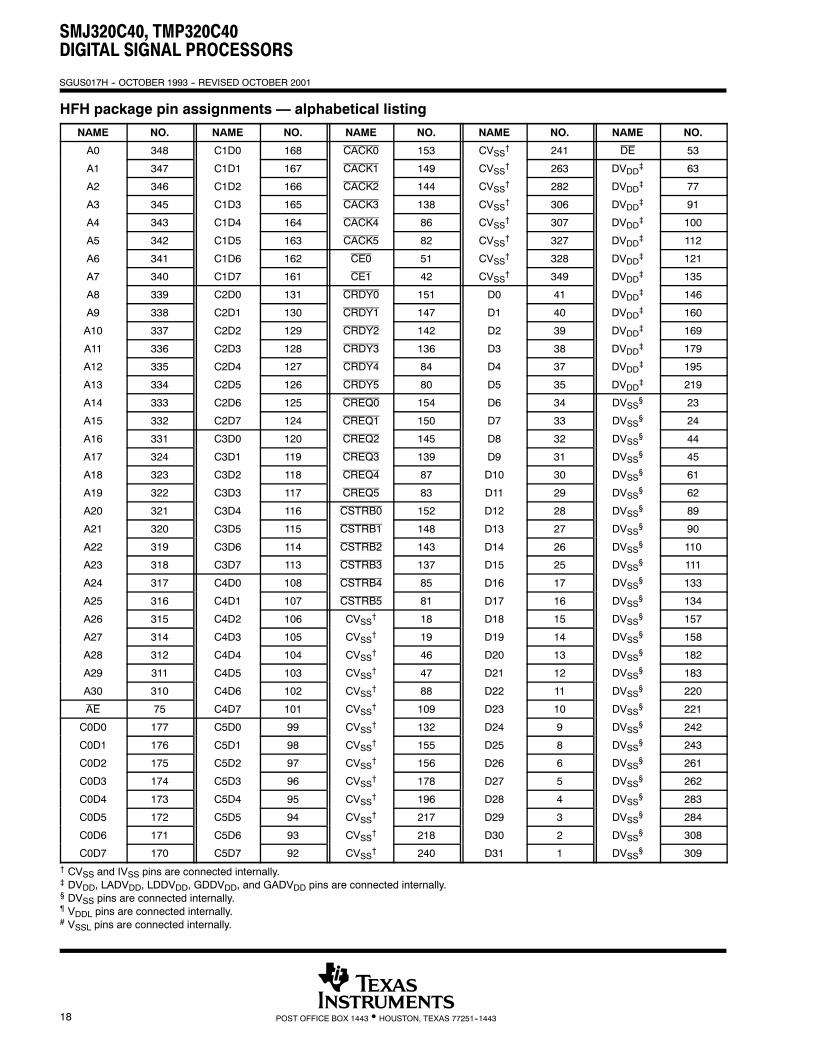
HFH package pin assignments — alphabetical listing
NAME NO. NAME NO. NAME NO. NAME NO. NAME NO.
A0 348 C1D0 168 CACK0 153 CVSS† 241 DE 53
A1 347 C1D1 167 CACK1 149 CVSS† 263 DVDD‡ 63
A2 346 C1D2 166 CACK2 144 CVSS† 282 DVDD‡ 77
A3 345 C1D3 165 CACK3 138 CVSS† 306 DVDD‡ 91
A4 343 C1D4 164 CACK4 86 CVSS† 307 DVDD‡ 100
A5 342 C1D5 163 CACK5 82 CVSS† 327 DVDD‡ 112
A6 341 C1D6 162 CE0 51 CVSS† 328 DVDD‡ 121
A7 340 C1D7 161 CE1 42 CVSS† 349 DVDD‡ 135
A8 339 C2D0 131 CRDY0 151 D0 41 DVDD‡ 146
A9 338 C2D1 130 CRDY1 147 D1 40 DVDD‡ 160
A10 337 C2D2 129 CRDY2 142 D2 39 DVDD‡ 169
A11 336 C2D3 128 CRDY3 136 D3 38 DVDD‡ 179
A12 335 C2D4 127 CRDY4 84 D4 37 DVDD‡ 195
A13 334 C2D5 126 CRDY5 80 D5 35 DVDD‡ 219
A14 333 C2D6 125 CREQ0 154 D6 34 DVSS§ 23
A15 332 C2D7 124 CREQ1 150 D7 33 DVSS§ 24
A16 331 C3D0 120 CREQ2 145 D8 32 DVSS§ 44
A17 324 C3D1 119 CREQ3 139 D9 31 DVSS§ 45
A18 323 C3D2 118 CREQ4 87 D10 30 DVSS§ 61
A19 322 C3D3 117 CREQ5 83 D11 29 DVSS§ 62
A20 321 C3D4 116 CSTRB0 152 D12 28 DVSS§ 89
A21 320 C3D5 115 CSTRB1 148 D13 27 DVSS§ 90
A22 319 C3D6 114 CSTRB2 143 D14 26 DVSS§ 110
A23 318 C3D7 113 CSTRB3 137 D15 25 DVSS§ 111
A24 317 C4D0 108 CSTRB4 85 D16 17 DVSS§ 133
A25 316 C4D1 107 CSTRB5 81 D17 16 DVSS§ 134
A26 315 C4D2 106 CVSS† 18 D18 15 DVSS§ 157
A27 314 C4D3 105 CVSS† 19 D19 14 DVSS§ 158
A28 312 C4D4 104 CVSS† 46 D20 13 DVSS§ 182
A29 311 C4D5 103 CVSS† 47 D21 12 DVSS§ 183
A30 310 C4D6 102 CVSS† 88 D22 11 DVSS§ 220
AE 75 C4D7 101 CVSS† 109 D23 10 DVSS§ 221
C0D0 177 C5D0 99 CVSS† 132 D24 9 DVSS§ 242
C0D1 176 C5D1 98 CVSS† 155 D25 8 DVSS§ 243
C0D2 175 C5D2 97 CVSS† 156 D26 6 DVSS§ 261
C0D3 174 C5D3 96 CVSS† 178 D27 5 DVSS§ 262
C0D4 173 C5D4 95 CVSS† 196 D28 4 DVSS§ 283
C0D5 172 C5D5 94 CVSS† 217 D29 3 DVSS§ 284
C0D6 171 C5D6 93 CVSS† 218 D30 2 DVSS§ 308
C0D7 170 C5D7 92 CVSS† 240 D31 1 DVSS§ 309† CVSS and IVSS pins are connected internally.‡ DVDD, LADVDD, LDDVDD, GDDVDD, and GADVDD pins are connected internally.§ DVSS pins are connected internally.¶ VDDL pins are connected internally.# VSSL pins are connected internally.
SMJ320C40, TMP320C40DIGITAL SIGNAL PROCESSORS
SGUS017H -- OCTOBER 1993 -- REVISED OCTOBER 2001
19POST OFFICE BOX 1443 • HOUSTON, TEXAS 77251--1443
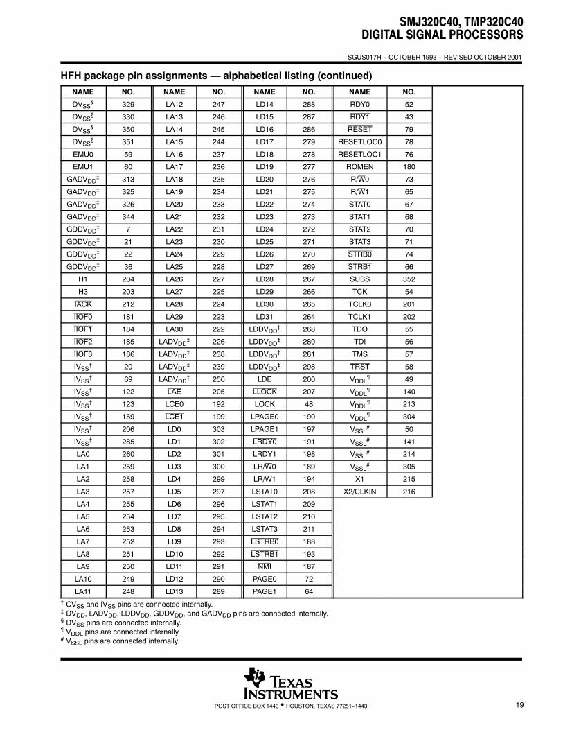
HFH package pin assignments — alphabetical listing (continued)
NAME NO. NAME NO. NAME NO. NAME NO.
DVSS§ 329 LA12 247 LD14 288 RDY0 52
DVSS§ 330 LA13 246 LD15 287 RDY1 43
DVSS§ 350 LA14 245 LD16 286 RESET 79
DVSS§ 351 LA15 244 LD17 279 RESETLOC0 78
EMU0 59 LA16 237 LD18 278 RESETLOC1 76
EMU1 60 LA17 236 LD19 277 ROMEN 180
GADVDD‡ 313 LA18 235 LD20 276 R/W0 73
GADVDD‡ 325 LA19 234 LD21 275 R/W1 65
GADVDD‡ 326 LA20 233 LD22 274 STAT0 67
GADVDD‡ 344 LA21 232 LD23 273 STAT1 68
GDDVDD‡ 7 LA22 231 LD24 272 STAT2 70
GDDVDD‡ 21 LA23 230 LD25 271 STAT3 71
GDDVDD‡ 22 LA24 229 LD26 270 STRB0 74
GDDVDD‡ 36 LA25 228 LD27 269 STRB1 66
H1 204 LA26 227 LD28 267 SUBS 352
H3 203 LA27 225 LD29 266 TCK 54
IACK 212 LA28 224 LD30 265 TCLK0 201
IIOF0 181 LA29 223 LD31 264 TCLK1 202
IIOF1 184 LA30 222 LDDVDD‡ 268 TDO 55
IIOF2 185 LADVDD‡ 226 LDDVDD‡ 280 TDI 56
IIOF3 186 LADVDD‡ 238 LDDVDD‡ 281 TMS 57
IVSS† 20 LADVDD‡ 239 LDDVDD‡ 298 TRST 58
IVSS† 69 LADVDD‡ 256 LDE 200 VDDL¶ 49
IVSS† 122 LAE 205 LLOCK 207 VDDL¶ 140
IVSS† 123 LCE0 192 LOCK 48 VDDL¶ 213
IVSS† 159 LCE1 199 LPAGE0 190 VDDL¶ 304
IVSS† 206 LD0 303 LPAGE1 197 VSSL# 50
IVSS† 285 LD1 302 LRDY0 191 VSSL# 141
LA0 260 LD2 301 LRDY1 198 VSSL# 214
LA1 259 LD3 300 LR/W0 189 VSSL# 305
LA2 258 LD4 299 LR/W1 194 X1 215
LA3 257 LD5 297 LSTAT0 208 X2/CLKIN 216
LA4 255 LD6 296 LSTAT1 209
LA5 254 LD7 295 LSTAT2 210
LA6 253 LD8 294 LSTAT3 211
LA7 252 LD9 293 LSTRB0 188
LA8 251 LD10 292 LSTRB1 193
LA9 250 LD11 291 NMI 187
LA10 249 LD12 290 PAGE0 72
LA11 248 LD13 289 PAGE1 64† CVSS and IVSS pins are connected internally.‡ DVDD, LADVDD, LDDVDD, GDDVDD, and GADVDD pins are connected internally.§ DVSS pins are connected internally.¶ VDDL pins are connected internally.# VSSL pins are connected internally.

SMJ320C40, TMP320C40DIGITAL SIGNAL PROCESSORS
SGUS017H -- OCTOBER 1993 -- REVISED OCTOBER 2001
20 POST OFFICE BOX 1443 • HOUSTON, TEXAS 77251--1443
HFH package pin assignments — numerical listing
NO. NAME NO. NAME NO. NAME NO. NAME NO. NAME
1 D31 41 D0 81 CSTRB5 121 DVDD‡ 161 C1D7
2 D30 42 CE1 82 CACK5 122 IVSS† 162 C1D6
3 D29 43 RDY1 83 CREQ5 123 IVSS† 163 C1D5
4 D28 44 DVSS§ 84 CRDY4 124 C2D7 164 C1D4
5 D27 45 DVSS§ 85 CSTRB4 125 C2D6 165 C1D3
6 D26 46 CVSS† 86 CACK4 126 C2D5 166 C1D2
7 GDDVDD‡ 47 CVSS† 87 CREQ4 127 C2D4 167 C1D1
8 D25 48 LOCK 88 CVSS† 128 C2D3 168 C1D0
9 D24 49 VDDL¶ 89 DVSS§ 129 C2D2 169 DVDD‡
10 D23 50 VSSL# 90 DVSS§ 130 C2D1 170 C0D7
11 D22 51 CE0 91 DVDD‡ 131 C2D0 171 C0D6
12 D21 52 RDY0 92 C5D7 132 CVSS† 172 C0D5
13 D20 53 DE 93 C5D6 133 DVSS§ 173 C0D4
14 D19 54 TCK 94 C5D5 134 DVSS§ 174 C0D3
15 D18 55 TDO 95 C5D4 135 DVDD‡ 175 C0D2
16 D17 56 TDI 96 C5D3 136 CRDY3 176 C0D1
17 D16 57 TMS 97 C5D2 137 CSTRB3 177 C0D0
18 CVSS† 58 TRST 98 C5D1 138 CACK3 178 CVSS†
19 CVSS† 59 EMU0 99 C5D0 139 CREQ3 179 DVDD‡
20 IVSS† 60 EMU1 100 DVDD‡ 140 VDDL¶ 180 ROMEN
21 GDDVDD‡ 61 DVSS§ 101 C4D7 141 VSSL# 181 IIOF0
22 GDDVDD‡ 62 DVSS§ 102 C4D6 142 CRDY2 182 DVSS§
23 DVSS§ 63 DVDD‡ 103 C4D5 143 CSTRB2 183 DVSS§
24 DVSS§ 64 PAGE1 104 C4D4 144 CACK2 184 IIOF1
25 D15 65 R/W1 105 C4D3 145 CREQ2 185 IIOF2
26 D14 66 STRB1 106 C4D2 146 DVDD‡ 186 IIOF3
27 D13 67 STAT0 107 C4D1 147 CRDY1 187 NMI
28 D12 68 STAT1 108 C4D0 148 CSTRB1 188 LSTRB0
29 D11 69 IVSS† 109 CVSS† 149 CACK1 189 LR/W0
30 D10 70 STAT2 110 DVSS§ 150 CREQ1 190 LPAGE0
31 D9 71 STAT3 111 DVSS§ 151 CRDY0 191 LRDY0
32 D8 72 PAGE0 112 DVDD‡ 152 CSTRB0 192 LCE0
33 D7 73 R/W0 113 C3D7 153 CACK0 193 LSTRB1
34 D6 74 STRB0 114 C3D6 154 CREQ0 194 LR/W1
35 D5 75 AE 115 C3D5 155 CVSS† 195 DVDD‡
36 GDDVDD‡ 76 RESETLOC1 116 C3D4 156 CVSS† 196 CVSS†
37 D4 77 DVDD‡ 117 C3D3 157 DVSS§ 197 LPAGE1
38 D3 78 RESETLOC0 118 C3D2 158 DVSS§ 198 LRDY1
39 D2 79 RESET 119 C3D1 159 IVSS† 199 LCE1
40 D1 80 CRDY5 120 C3D0 160 DVDD‡ 200 LDE† CVSS and IVSS pins are connected internally.‡ DVDD, LADVDD, LDDVDD, GDDVDD, and GADVDD pins are connected internally.§ DVSS pins are connected internally.¶ VDDL pins are connected internally.# VSSL pins are connected internally.

SMJ320C40, TMP320C40DIGITAL SIGNAL PROCESSORS
SGUS017H -- OCTOBER 1993 -- REVISED OCTOBER 2001
21POST OFFICE BOX 1443 • HOUSTON, TEXAS 77251--1443
HFH package pin assignments — numerical listing (continued)
NO. NAME NO. NAME NO. NAME NO. NAME
201 TCLK0 241 CVSS† 281 LDDVDD‡ 321 A20
202 TCLK1 242 DVSS§ 282 CVSS† 322 A19
203 H3 243 DVSS§ 283 DVSS§ 323 A18
204 H1 244 LA15 284 DVSS§ 324 A17
205 LAE 245 LA14 285 IVSS† 325 GADVDD‡
206 IVSS† 246 LA13 286 LD16 326 GADVDD‡
207 LLOCK 247 LA12 287 LD15 327 CVSS†
208 LSTAT0 248 LA11 288 LD14 328 CVSS†
209 LSTAT1 249 LA10 289 LD13 329 DVSS§
210 LSTAT2 250 LA9 290 LD12 330 DVSS§
211 LSTAT3 251 LA8 291 LD11 331 A16
212 IACK 252 LA7 292 LD10 332 A15
213 VDDL¶ 253 LA6 293 LD9 333 A14
214 VSSL# 254 LA5 294 LD8 334 A13
215 X1 255 LA4 295 LD7 335 A12
216 X2/CLKIN 256 LADVDD‡ 296 LD6 336 A11
217 CVSS† 257 LA3 297 LD5 337 A10
218 CVSS† 258 LA2 298 LDDVDD‡ 338 A9
219 DVDD‡ 259 LA1 299 LD4 339 A8
220 DVSS§ 260 LA0 300 LD3 340 A7
221 DVSS§ 261 DVSS§ 301 LD2 341 A6
222 LA30 262 DVSS§ 302 LD1 342 A5
223 LA29 263 CVSS† 303 LD0 343 A4
224 LA28 264 LD31 304 VDDL¶ 344 GADVDD‡
225 LA27 265 LD30 305 VSSL# 345 A3
226 LADVDD‡ 266 LD29 306 CVSS† 346 A2
227 LA26 267 LD28 307 CVSS† 347 A1
228 LA25 268 LDDVDD‡ 308 DVSS§ 348 A0
229 LA24 269 LD27 309 DVSS§ 349 CVSS†
230 LA23 270 LD26 310 A30 350 DVSS§
231 LA22 271 LD25 311 A29 351 DVSS§
232 LA21 272 LD24 312 A28 352 SUBS
233 LA20 273 LD23 313 GADVDD‡
234 LA19 274 LD22 314 A27
235 LA18 275 LD21 315 A26
236 LA17 276 LD20 316 A25
237 LA16 277 LD19 317 A24
238 LADVDD‡ 278 LD18 318 A23
239 LADVDD‡ 279 LD17 319 A22
240 CVSS† 280 LDDVDD‡ 320 A21† CVSS and IVSS pins are connected internally.‡ DVDD, LADVDD, LDDVDD, GDDVDD, and GADVDD pins are connected internally.§ DVSS pins are connected internally.¶ VDDL pins are connected internally.# VSSL pins are connected internally.
SMJ320C40, TMP320C40DIGITAL SIGNAL PROCESSORS
SGUS017H -- OCTOBER 1993 -- REVISED OCTOBER 2001
22 POST OFFICE BOX 1443 • HOUSTON, TEXAS 77251--1443
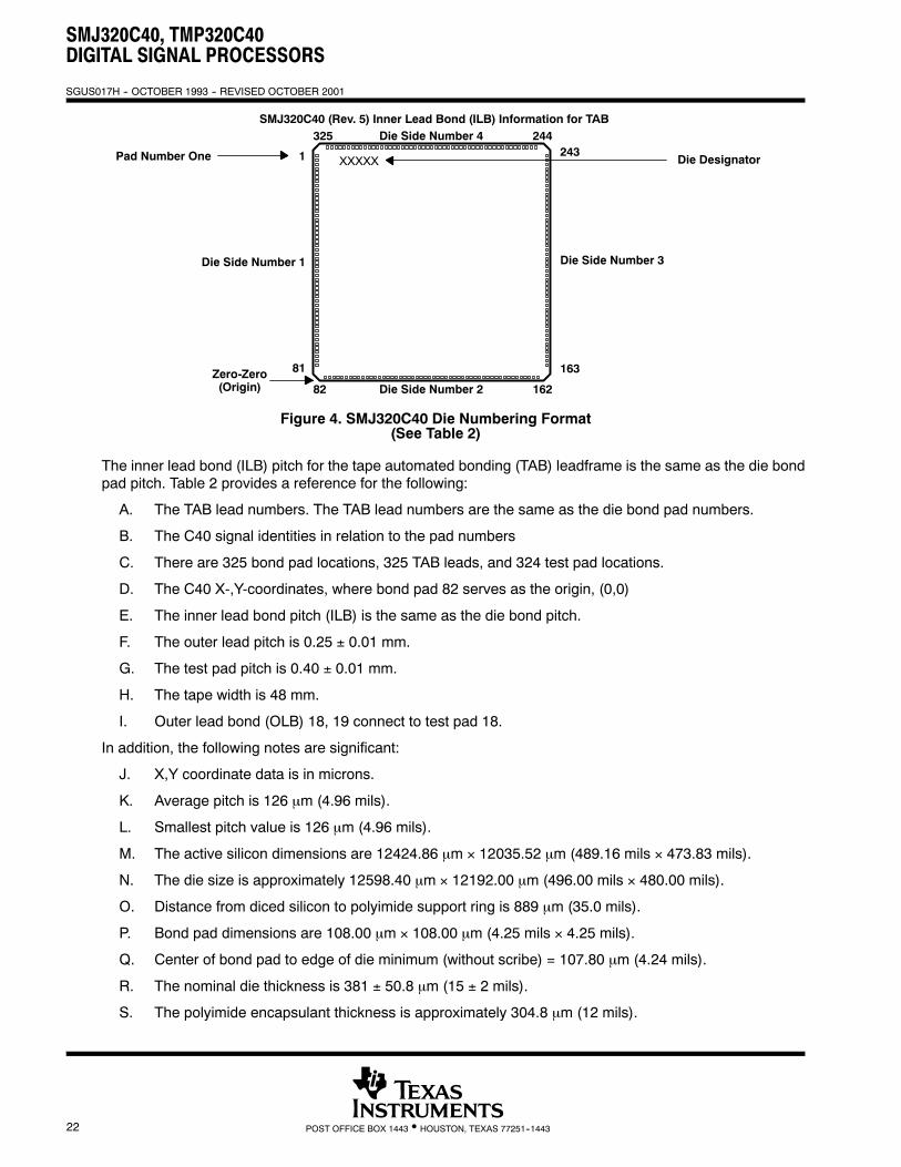
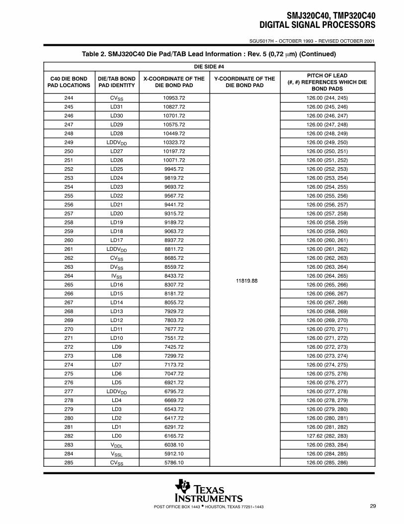
325 244Die Side Number 4
Pad Number One 1
Die Side Number 1
81Zero-Zero(Origin) 82 162Die Side Number 2
243
Die Side Number 3
163
Die Designator
SMJ320C40 (Rev. 5) Inner Lead Bond (ILB) Information for TAB
XXXXX
Figure 4. SMJ320C40 Die Numbering Format(See Table 2)
The inner lead bond (ILB) pitch for the tape automated bonding (TAB) leadframe is the same as the die bondpad pitch. Table 2 provides a reference for the following:
A. The TAB lead numbers. The TAB lead numbers are the same as the die bond pad numbers.
B. The C40 signal identities in relation to the pad numbers
C. There are 325 bond pad locations, 325 TAB leads, and 324 test pad locations.
D. The C40 X-,Y-coordinates, where bond pad 82 serves as the origin, (0,0)
E. The inner lead bond pitch (ILB) is the same as the die bond pitch.
F. The outer lead pitch is 0.25 ± 0.01 mm.
G. The test pad pitch is 0.40 ± 0.01 mm.
H. The tape width is 48 mm.
I. Outer lead bond (OLB) 18, 19 connect to test pad 18.
In addition, the following notes are significant:
J. X,Y coordinate data is in microns.
K. Average pitch is 126 μm (4.96 mils).
L. Smallest pitch value is 126 μm (4.96 mils).
M. The active silicon dimensions are 12424.86 μm × 12035.52 μm (489.16 mils × 473.83 mils).
N. The die size is approximately 12598.40 μm × 12192.00 μm (496.00 mils × 480.00 mils).
O. Distance from diced silicon to polyimide support ring is 889 μm (35.0 mils).
P. Bond pad dimensions are 108.00 μm × 108.00 μm (4.25 mils × 4.25 mils).
Q. Center of bond pad to edge of die minimum (without scribe) = 107.80 μm (4.24 mils).
R. The nominal die thickness is 381 ± 50.8 μm (15 ± 2 mils).
S. The polyimide encapsulant thickness is approximately 304.8 μm (12 mils).
SMJ320C40, TMP320C40DIGITAL SIGNAL PROCESSORS
SGUS017H -- OCTOBER 1993 -- REVISED OCTOBER 2001
23POST OFFICE BOX 1443 • HOUSTON, TEXAS 77251--1443
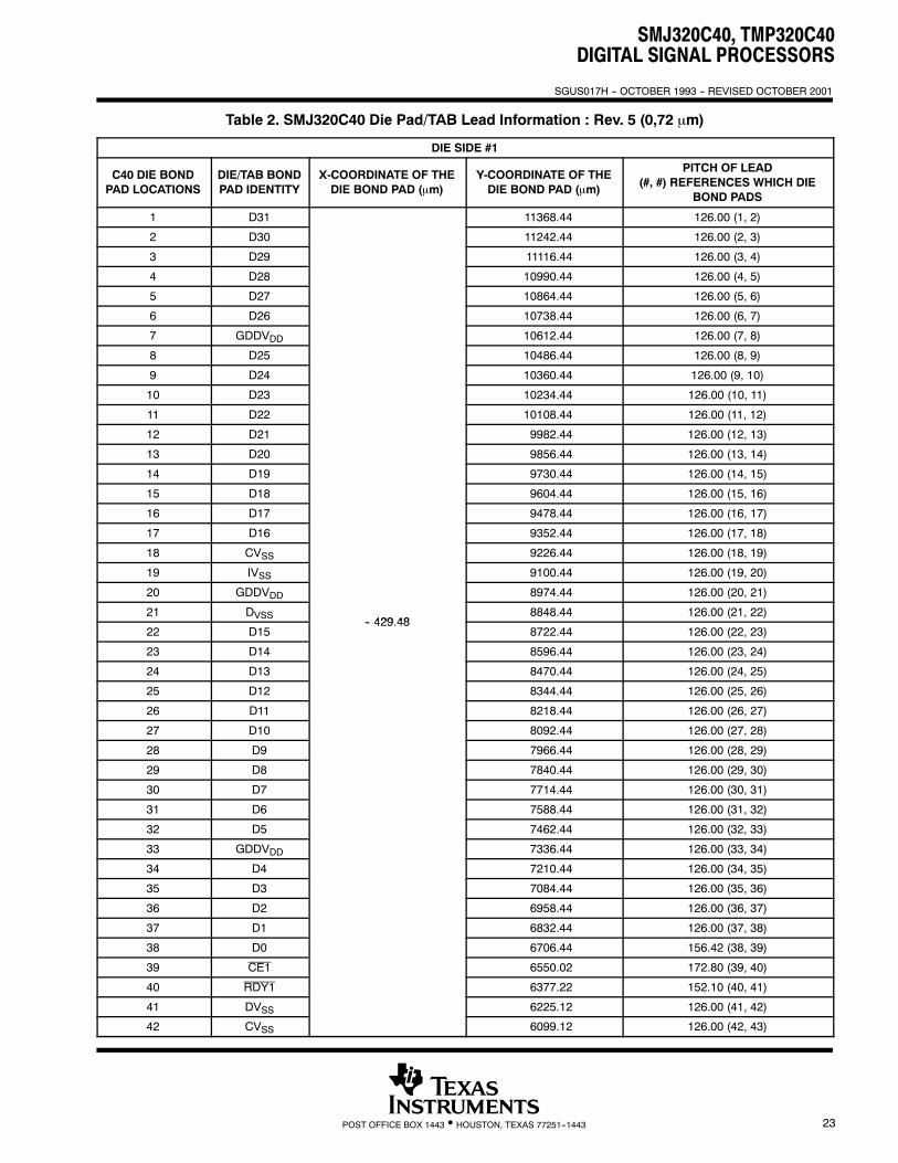
Table 2. SMJ320C40 Die Pad/TAB Lead Information : Rev. 5 (0,72 μm)
DIE SIDE #1
C40 DIE BONDPAD LOCATIONS
DIE/TAB BONDPAD IDENTITY
X-COORDINATE OF THEDIE BOND PAD (μm)
Y-COORDINATE OF THEDIE BOND PAD (μm)
PITCH OF LEAD(#, #) REFERENCES WHICH DIE
BOND PADS
1 D31 11368.44 126.00 (1, 2)
2 D30 11242.44 126.00 (2, 3)
3 D29 11116.44 126.00 (3, 4)
4 D28 10990.44 126.00 (4, 5)
5 D27 10864.44 126.00 (5, 6)
6 D26 10738.44 126.00 (6, 7)
7 GDDVDD 10612.44 126.00 (7, 8)
8 D25 10486.44 126.00 (8, 9)
9 D24 10360.44 126.00 (9, 10)
10 D23 10234.44 126.00 (10, 11)
11 D22 10108.44 126.00 (11, 12)
12 D21 9982.44 126.00 (12, 13)
13 D20 9856.44 126.00 (13, 14)
14 D19 9730.44 126.00 (14, 15)
15 D18 9604.44 126.00 (15, 16)
16 D17 9478.44 126.00 (16, 17)
17 D16 9352.44 126.00 (17, 18)
18 CVSS 9226.44 126.00 (18, 19)
19 IVSS 9100.44 126.00 (19, 20)
20 GDDVDD 8974.44 126.00 (20, 21)
21 DVSS429 48
8848.44 126.00 (21, 22)
22 D15-- 429.48
8722.44 126.00 (22, 23)
23 D14 8596.44 126.00 (23, 24)
24 D13 8470.44 126.00 (24, 25)
25 D12 8344.44 126.00 (25, 26)
26 D11 8218.44 126.00 (26, 27)
27 D10 8092.44 126.00 (27, 28)
28 D9 7966.44 126.00 (28, 29)
29 D8 7840.44 126.00 (29, 30)
30 D7 7714.44 126.00 (30, 31)
31 D6 7588.44 126.00 (31, 32)
32 D5 7462.44 126.00 (32, 33)
33 GDDVDD 7336.44 126.00 (33, 34)
34 D4 7210.44 126.00 (34, 35)
35 D3 7084.44 126.00 (35, 36)
36 D2 6958.44 126.00 (36, 37)
37 D1 6832.44 126.00 (37, 38)
38 D0 6706.44 156.42 (38, 39)
39 CE1 6550.02 172.80 (39, 40)
40 RDY1 6377.22 152.10 (40, 41)
41 DVSS 6225.12 126.00 (41, 42)
42 CVSS 6099.12 126.00 (42, 43)
SMJ320C40, TMP320C40DIGITAL SIGNAL PROCESSORS
SGUS017H -- OCTOBER 1993 -- REVISED OCTOBER 2001
24 POST OFFICE BOX 1443 • HOUSTON, TEXAS 77251--1443
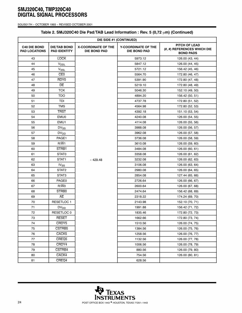
Table 2. SMJ320C40 Die Pad/TAB Lead Information : Rev. 5 (0,72 μm) (Continued)
DIE SIDE #1 (CONTINUED)
C40 DIE BONDPAD LOCATIONS
DIE/TAB BONDPAD IDENTITY
X-COORDINATE OF THEDIE BOND PAD
Y-COORDINATE OF THEDIE BOND PAD
PITCH OF LEAD(#, #) REFERENCES WHICH DIE
BOND PADS
43 LOCK 5973.12 126.00 (43, 44)
44 VDDL 5847.12 126.00 (44, 45)
45 VSSL 5721.12 156.42 (45, 46)
46 CE0 5564.70 172.80 (46, 47)
47 RDY0 5391.90 172.80 (47, 48)
48 DE 5219.10 172.80 (48, 49)
49 TCK 5046.30 152.10 (49, 50)
50 TDO 4894.20 156.42 (50, 51)
51 TDI 4737.78 172.80 (51, 52)
52 TMS 4564.98 172.80 (52, 53)
53 TRST 4392.18 151.10 (53, 54)
54 EMU0 4240.08 126.00 (54, 55)
55 EMU1 4114.08 126.00 (55, 56)
56 DVSS 3988.08 126.00 (56, 57)
57 DVDD 3962.08 126.00 (57, 58)
58 PAGE1 3736.08 126.00 (58, 59)
59 R/W1 3610.08 126.00 (59, 60)
60 STRB1 3484.08 126.00 (60, 61)
61 STAT0 3358.08 126.00 (61, 62)
62 STAT1 -- 429.48 3232.08 126.00 (62, 63)
63 IVSS
429.48
3106.08 126.00 (63, 64)
64 STAT2 2980.08 126.00 (64, 65)
65 STAT3 2854.08 127.44 (65, 66)
66 PAGE0 2726.64 126.00 (66, 67)
67 R/W0 2600.64 126.00 (67, 68)
68 STRB0 2474.64 156.42 (68, 69)
69 AE 2318.22 174.24 (69, 70)
70 RESETLOC 1 2143.98 152.10 (70, 71)
71 DVDD 1991.88 156.42 (71, 72)
72 RESETLOC 0 1835.46 172.80 (72, 73)
73 RESET 1662.66 172.80 (73, 74)
74 CRDY5 1510.56 126.00 (74, 75)
75 CSTRB5 1384.56 126.00 (75, 76)
76 CACK5 1258.56 126.00 (76, 77)
77 CREQ5 1132.56 126.00 (77, 78)
78 CRDY4 1006.56 126.00 (78, 79)
79 CSTRB4 880.56 126.00 (79, 80)
80 CACK4 754.56 126.00 (80, 81)
81 CREQ4 628.56

SMJ320C40, TMP320C40DIGITAL SIGNAL PROCESSORS
SGUS017H -- OCTOBER 1993 -- REVISED OCTOBER 2001
25POST OFFICE BOX 1443 • HOUSTON, TEXAS 77251--1443
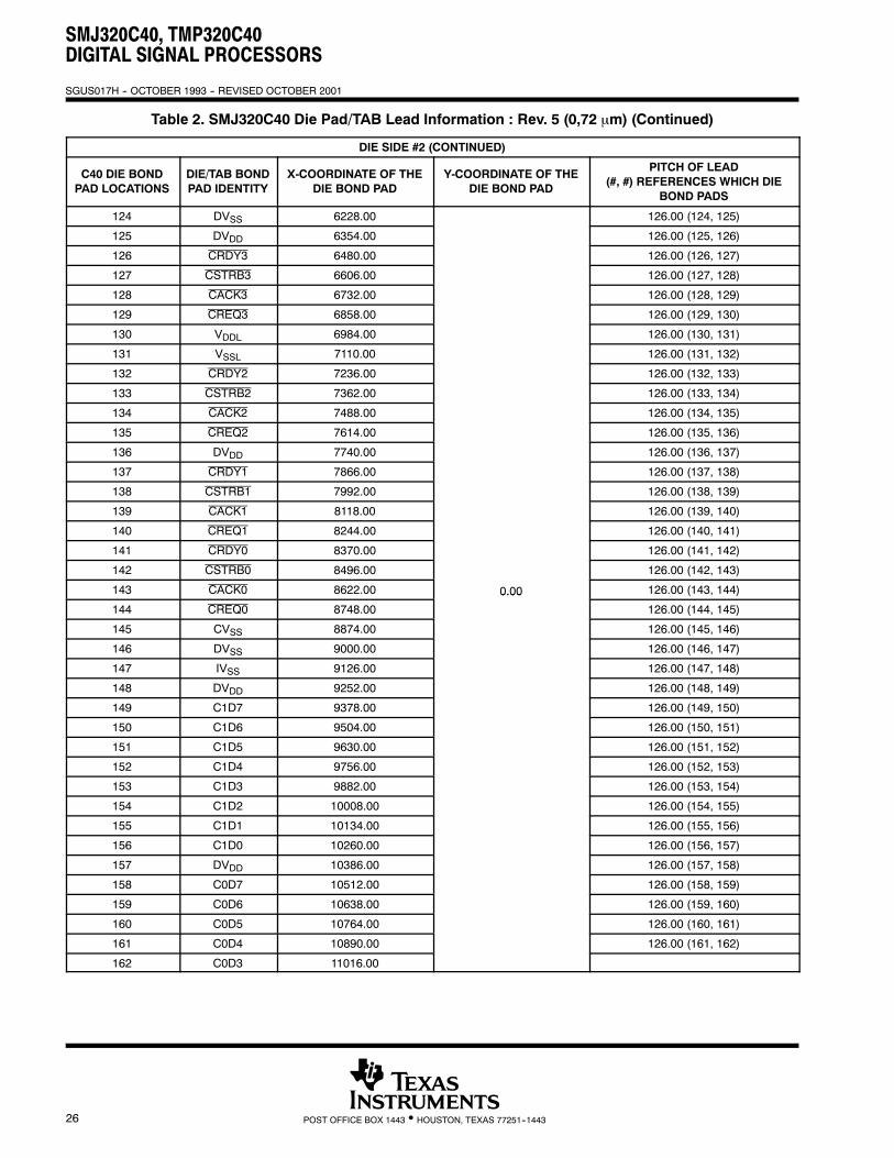
Table 2. SMJ320C40 Die Pad/TAB Lead Information : Rev. 5 (0,72 μm) (Continued)
DIE SIDE #2
C40 DIE BONDPAD LOCATIONS
DIE/TAB BONDPAD IDENTITY
X-COORDINATE OF THEDIE BOND PAD
Y-COORDINATE OF THEDIE BOND PAD
PITCH OF LEAD(#, #) REFERENCES WHICH DIE
BOND PADS
82 CVSS 0.00 1062.00 (82, 83)
83 DVSS 1062.00 126.00 (83, 84)
84 DVDD 1188.00 126.00 (84, 85)
85 C5D7 1314.00 126.00 (85, 86)
86 C5D6 1440.00 126.00 (86, 87)
87 C5D5 1566.00 126.00 (87, 88)
88 C5D4 1692.00 126.00 (88, 89)
89 C5D3 1818.00 126.00 (89, 90)
90 C5D2 1944.00 126.00 (90, 91)
91 C5D1 2070.00 126.00 (91, 92)
92 C5D0 2196.00 126.00 (92, 93)
93 DVDD 2322.00 126.00 (93, 94)
94 C4D7 2448.00 126.00 (94, 95)
95 C4D6 2574.00 126.00 (95, 96)
96 C4D5 2700.00 126.00 (96, 97)
97 C4D4 2813.40 126.00 (97, 98)
98 C4D3 2952.00 126.00 (98, 99)
99 C4D2 3078.00 126.00 (99, 100)
100 C4D1 3204.00 126.00 (100, 101)
101 C4D0 3330.00 126.00 (101, 102)
102 CVSS 3456.000 00
126.00 (102, 103)
103 DVSS 3582.000.00
126.00 (103, 104)
104 DVDD 3708.00 126.00 (104, 105)
105 C3D7 3834.00 126.00 (105, 106)
106 C3D6 3960.00 126.00 (106, 107)
107 C3D5 4086.00 126.00 (107, 108)
108 C3D4 4212.00 126.00 (108, 109)
109 C3D3 4338.00 126.00 (109, 110)
110 C3D2 4464.00 126.00 (110, 111)
111 C3D1 4590.00 126.00 (111, 112)
112 C3D0 4716.00 126.00 (112, 113)
113 DVDD 4842.00 126.00 (113, 114)
114 IVSS 4968.00 126.00 (114, 115)
115 C2D7 5094.00 126.00 (115, 116)
116 C2D6 5220.00 126.00 (116, 117)
117 C2D5 5346.00 126.00 (117, 118)
118 C2D4 5472.00 126.00 (118, 119)
119 C2D3 5598.00 126.00 (119, 120)
120 C2D2 5724.00 126.00 (120, 121)
121 C2D1 5850.00 126.00 (121, 122)
122 C2D0 5976.00 126.00 (122, 123)
123 CVSS 6102.00 126.00 (123, 124)
SMJ320C40, TMP320C40DIGITAL SIGNAL PROCESSORS
SGUS017H -- OCTOBER 1993 -- REVISED OCTOBER 2001
26 POST OFFICE BOX 1443 • HOUSTON, TEXAS 77251--1443
Table 2. SMJ320C40 Die Pad/TAB Lead Information : Rev. 5 (0,72 μm) (Continued)
DIE SIDE #2 (CONTINUED)
C40 DIE BONDPAD LOCATIONS
DIE/TAB BONDPAD IDENTITY
X-COORDINATE OF THEDIE BOND PAD
Y-COORDINATE OF THEDIE BOND PAD
PITCH OF LEAD(#, #) REFERENCES WHICH DIE
BOND PADS
124 DVSS 6228.00 126.00 (124, 125)
125 DVDD 6354.00 126.00 (125, 126)
126 CRDY3 6480.00 126.00 (126, 127)
127 CSTRB3 6606.00 126.00 (127, 128)
128 CACK3 6732.00 126.00 (128, 129)
129 CREQ3 6858.00 126.00 (129, 130)
130 VDDL 6984.00 126.00 (130, 131)
131 VSSL 7110.00 126.00 (131, 132)
132 CRDY2 7236.00 126.00 (132, 133)
133 CSTRB2 7362.00 126.00 (133, 134)
134 CACK2 7488.00 126.00 (134, 135)
135 CREQ2 7614.00 126.00 (135, 136)
136 DVDD 7740.00 126.00 (136, 137)
137 CRDY1 7866.00 126.00 (137, 138)
138 CSTRB1 7992.00 126.00 (138, 139)
139 CACK1 8118.00 126.00 (139, 140)
140 CREQ1 8244.00 126.00 (140, 141)
141 CRDY0 8370.00 126.00 (141, 142)
142 CSTRB0 8496.00 126.00 (142, 143)
143 CACK0 8622.00 0.00 126.00 (143, 144)
144 CREQ0 8748.00
0.00
126.00 (144, 145)
145 CVSS 8874.00 126.00 (145, 146)
146 DVSS 9000.00 126.00 (146, 147)
147 IVSS 9126.00 126.00 (147, 148)
148 DVDD 9252.00 126.00 (148, 149)
149 C1D7 9378.00 126.00 (149, 150)
150 C1D6 9504.00 126.00 (150, 151)
151 C1D5 9630.00 126.00 (151, 152)
152 C1D4 9756.00 126.00 (152, 153)
153 C1D3 9882.00 126.00 (153, 154)
154 C1D2 10008.00 126.00 (154, 155)
155 C1D1 10134.00 126.00 (155, 156)
156 C1D0 10260.00 126.00 (156, 157)
157 DVDD 10386.00 126.00 (157, 158)
158 C0D7 10512.00 126.00 (158, 159)
159 C0D6 10638.00 126.00 (159, 160)
160 C0D5 10764.00 126.00 (160, 161)
161 C0D4 10890.00 126.00 (161, 162)
162 C0D3 11016.00

SMJ320C40, TMP320C40DIGITAL SIGNAL PROCESSORS
SGUS017H -- OCTOBER 1993 -- REVISED OCTOBER 2001
27POST OFFICE BOX 1443 • HOUSTON, TEXAS 77251--1443
Table 2. SMJ320C40 Die Pad/TAB Lead Information : Rev. 5 (0,72 μm) (Continued)
DIE SIDE #3
C40 DIE BONDPAD LOCATIONS
DIE/TAB BONDPAD IDENTITY
X-COORDINATE OF THEDIE BOND PAD
Y-COORDINATE OF THEDIE BOND PAD
PITCH OF LEAD(#, #) REFERENCES WHICH DIE
BOND PADS
163 C0D2 810.00 126.00 (163, 164)
164 C0D1 936.00 126.00 (164, 165)
165 C0D0 1062.00 126.00 (165, 166)
166 CVSS 1188.00 126.00 (166, 167)
167 DVDD 1314.00 156.42 (167, 168)
168 ROMEN 1470.42 152.46 (168, 169)
169 IIOF0 1622.88 126.00 (169, 170)
170 DVSS 1748.88 126.00 (170, 171)
171 IIOF1 1874.88 126.00 (171, 172)
172 IIOF2 2000.88 126.00 (172, 173)
173 IIOF3 2126.88 156.42 (173, 174)
174 NMI 2283.30 152.10 (174, 175)
175 LSTRB0 2435.40 126.00 (175, 176)
176 LR/W0 2561.40 126.00 (176, 177)
177 LPAGE0 2687.40 156.42 (177, 178)
178 LRDY0 2843.82 172.80 (178, 179)
179 LCE0 3016.62 152.10 (179, 180)
180 LSTRB1 3168.72 126.00 (180, 181)
181 LR/W1 3294.72 126.00 (181, 182)
182 DVDD 3420.72 126.00 (182, 183)
183 CVSS11779 74
3546.72 126.00 (183, 184)
184 LPAGE111779.74
3672.72 156.42 (184, 185)
185 LRDY1 3829.14 172.80 (185, 186)
186 LCE1 4001.94 172.80 (186, 187)
187 LDE 4174.74 152.10 (187, 188)
188 TCLK0 4326.84 126.00 (188, 189)
189 TCLK1 4452.84 126.00 (189, 190)
190 H3 4578.84 126.00 (190, 191)
191 H1 4704.84 156.42 (191, 192)
192 LAE 4861.26 152.10 (192, 193)
193 IVSS 5013.36 126.00 (193, 194)
194 LLOCK 5139.36 126.00 (194, 195)
195 LSTAT0 5265.36 126.00 (195, 196)
196 LSTAT1 5391.36 126.00 (196, 197)
197 LSTAT2 5517.36 126.00 (197, 198)
198 LSTAT3 5643.36 127.44 (198, 199)
199 IACK 5770.80 126.00 (199, 200)
200 VDDL 5896.80 126.00 (200, 201)
201 VSSL 6022.80 131.94 (201, 202)
202 X1 6154.74 171.58 (202, 203)
203 X2/CLKIN 6326.28 168.12 (203, 204)
204 CVSS 6494.40 126.00 (204, 205)

SMJ320C40, TMP320C40DIGITAL SIGNAL PROCESSORS
SGUS017H -- OCTOBER 1993 -- REVISED OCTOBER 2001
28 POST OFFICE BOX 1443 • HOUSTON, TEXAS 77251--1443
Table 2. SMJ320C40 Die Pad/TAB Lead Information : Rev. 5 (0,72 μm) (Continued)
DIE SIDE #3 (CONTINUED)
C40 DIE BONDPAD LOCATIONS
DIE/TAB BONDPAD IDENTITY
X-COORDINATE OF THEDIE BOND PAD
Y-COORDINATE OF THEDIE BOND PAD
PITCH OF LEAD(#, #) REFERENCES WHICH DIE
BOND PADS
205 DVDD 6620.40 126.00 (205, 206)
206 DVSS 6746.40 127.44 (206, 207)
207 LA30 6873.84 126.00 (207, 208)
208 LA29 6999.84 126.00 (208, 209)
209 LA28 7125.84 126.00 (209, 210)
210 LA27 7251.84 126.00 (210, 211)
211 LADVDD 7377.84 126.00 (211, 212)
212 LA26 7503.84 126.00 (212, 213)
213 LA25 7629.84 126.00 (213, 214)
214 LA24 7755.84 126.00 (214, 215)
215 LA23 7881.84 126.00 (215, 216)
216 LA22 8007.84 126.00 (216, 217)
217 LA21 8133.84 126.00 (217, 218)
218 LA20 8259.84 126.00 (218, 219)
219 LA19 8385.84 126.00 (219, 220)
220 LA18 8511.84 126.00 (220, 221)
221 LA17 8637.84 126.00 (221, 222)
222 LA16 8763.84 126.00 (222, 223)
223 LADVDD 8889.84 126.00 (223, 224)
224 CVSS 11779.74 9015.84 126.00 (224, 225)
225 DVSS 9141.84 126.00 (225, 226)
226 LA15 9267.84 126.00 (226, 227)
227 LA14 9393.84 126.00 (227, 228)
228 LA13 9519.84 126.00 (228, 229)
229 LA12 9645.84 126.00 (229, 230)
230 LA11 9771.84 126.00 (230, 231)
231 LA10 9897.84 126.00 (231, 232)
232 LA9 10023.84 126.00 (232, 233)
233 LA8 10149.84 126.00 (233, 234)
234 LA7 10275.84 126.00 (234, 235)
235 LA6 10401.84 126.00 (235, 236)
236 LA5 10527.84 126.00 (236, 237)
237 LA4 10653.84 126.00 (237, 238)
238 LADVDD 10779.84 126.00 (238, 239)
239 LA3 10905.84 126.00 (239, 240)
240 LA2 11031.84 126.00 (240, 241)
241 LA1 11157.84 126.00 (241, 242)
242 LA0 11283.84 205.92 (242, 243)
243 DVSS 11489.76
SMJ320C40, TMP320C40DIGITAL SIGNAL PROCESSORS
SGUS017H -- OCTOBER 1993 -- REVISED OCTOBER 2001
29POST OFFICE BOX 1443 • HOUSTON, TEXAS 77251--1443
Table 2. SMJ320C40 Die Pad/TAB Lead Information : Rev. 5 (0,72 μm) (Continued)
DIE SIDE #4
C40 DIE BONDPAD LOCATIONS
DIE/TAB BONDPAD IDENTITY
X-COORDINATE OF THEDIE BOND PAD
Y-COORDINATE OF THEDIE BOND PAD
PITCH OF LEAD(#, #) REFERENCES WHICH DIE
BOND PADS
244 CVSS 10953.72 126.00 (244, 245)
245 LD31 10827.72 126.00 (245, 246)
246 LD30 10701.72 126.00 (246, 247)
247 LD29 10575.72 126.00 (247, 248)
248 LD28 10449.72 126.00 (248, 249)
249 LDDVDD 10323.72 126.00 (249, 250)
250 LD27 10197.72 126.00 (250, 251)
251 LD26 10071.72 126.00 (251, 252)
252 LD25 9945.72 126.00 (252, 253)
253 LD24 9819.72 126.00 (253, 254)
254 LD23 9693.72 126.00 (254, 255)
255 LD22 9567.72 126.00 (255, 256)
256 LD21 9441.72 126.00 (256, 257)
257 LD20 9315.72 126.00 (257, 258)
258 LD19 9189.72 126.00 (258, 259)
259 LD18 9063.72 126.00 (259, 260)
260 LD17 8937.72 126.00 (260, 261)
261 LDDVDD 8811.72 126.00 (261, 262)
262 CVSS 8685.72 126.00 (262, 263)
263 DVSS 8559.72 126.00 (263, 264)
264 IVSS 8433.7211819 88
126.00 (264, 265)
265 LD16 8307.7211819.88
126.00 (265, 266)
266 LD15 8181.72 126.00 (266, 267)
267 LD14 8055.72 126.00 (267, 268)
268 LD13 7929.72 126.00 (268, 269)
269 LD12 7803.72 126.00 (269, 270)
270 LD11 7677.72 126.00 (270, 271)
271 LD10 7551.72 126.00 (271, 272)
272 LD9 7425.72 126.00 (272, 273)
273 LD8 7299.72 126.00 (273, 274)
274 LD7 7173.72 126.00 (274, 275)
275 LD6 7047.72 126.00 (275, 276)
276 LD5 6921.72 126.00 (276, 277)
277 LDDVDD 6795.72 126.00 (277, 278)
278 LD4 6669.72 126.00 (278, 279)
279 LD3 6543.72 126.00 (279, 280)
280 LD2 6417.72 126.00 (280, 281)
281 LD1 6291.72 126.00 (281, 282)
282 LD0 6165.72 127.62 (282, 283)
283 VDDL 6038.10 126.00 (283, 284)
284 VSSL 5912.10 126.00 (284, 285)
285 CVSS 5786.10 126.00 (285, 286)

SMJ320C40, TMP320C40DIGITAL SIGNAL PROCESSORS
SGUS017H -- OCTOBER 1993 -- REVISED OCTOBER 2001
30 POST OFFICE BOX 1443 • HOUSTON, TEXAS 77251--1443
Table 2. SMJ320C40 Die Pad/TAB Lead Information : Rev. 5 (0,72 μm) (Continued)
DIE SIDE #4 (CONTINUED)
C40 DIE BONDPAD LOCATIONS
DIE/TAB BONDPAD IDENTITY
X-COORDINATE OF THEDIE BOND PAD
Y-COORDINATE OF THEDIE BOND PAD
PITCH OF LEAD(#, #) REFERENCES WHICH DIE
BOND PADS
286 DVSS 5660.10 126.00 (286, 287)
287 A30 5534.10 126.00 (287, 288)
288 A29 5408.10 126.00 (288, 289)
289 A28 5282.10 126.00 (289, 290)
290 GADVDD 5156.10 126.00 (290, 291)
291 A27 5030.10 126.00 (291, 292)
292 A26 4904.10 126.00 (292, 293)
293 A25 4778.10 126.00 (293, 294)
294 A24 4652.10 126.00 (294, 295)
295 A23 4526.10 126.00 (295, 296)
296 A22 4400.10 126.00 (296, 297)
297 A21 4274.10 126.00 (297, 298)
298 A20 4148.10 126.00 (298, 299)
299 A19 4022.10 126.00 (299, 300)
300 A18 3896.10 126.00 (300, 301)
301 A17 3770.10 126.00 (301, 302)
302 GADVDD 3644.10 126.00 (302, 303)
303 CVSS 3518.10 126.00 (303, 304)
304 DVSS 3392.10 126.00 (304, 305)
305 A16 3266.1011819 88
126.00 (305, 306)
306 A15 3140.1011819.88
126.00 (306, 307)
307 A14 3014.10 126.00 (307, 308)
308 A13 2888.10 126.00 (308, 309)
309 A12 2762.10 126.00 (309, 310)
310 A11 2636.10 126.00 (310, 311)
311 A10 2510.10 126.00 (311, 312)
312 A9 2384.10 126.00 (312, 313)
313 A8 2258.10 126.00 (313, 314)
314 A7 2132.10 126.00 (314, 315)
315 A6 2006.10 126.00 (315, 316)
316 A5 1880.10 126.00 (316, 317)
317 A4 1754.10 126.00 (317, 318)
318 GADVDD 1628.10 126.00 (318, 319)
319 A3 1502.10 126.00 (319, 320)
320 A2 1376.10 126.00 (320, 321)
321 A1 1250.10 126.00 (321, 322)
322 A0 1124.10 126.00 (322, 323)
323 CVSS 998.10 558.00 (323, 324)
324 DVSS 440.10 630.00 (324, 325)
325 SUBS -- 189.90

SMJ320C40, TMP320C40DIGITAL SIGNAL PROCESSORS
SGUS017H -- OCTOBER 1993 -- REVISED OCTOBER 2001
31POST OFFICE BOX 1443 • HOUSTON, TEXAS 77251--1443
SMJ320C40 device nomenclature
SMJ 320 C 40 HFH M 40
PREFIX:SMJ = MIL-PRF-38535SM = Standard Processing
DEVICE FAMILY:320 = SMJ320 DSP Family
TECHNOLOGY:C = CMOS PACKAGE TYPE:
GF = 325-Pin Ceramic Staggered PGAHFH = 352-Lead Ceramic Quad Flat Pack
(nonconductive tie-bar)
SPEED RANGE:40 = 40 MHz50 = 50 MHz60 = 60 MHz
TEMPERATURE RANGE:M = --55°C to 125°CS = --55°C to 100°C
DEVICE:40 = 320C40
SMJ 320 C 40 TAB M 40 /10
PREFIX:SMJ = MIL-PRF-38535SM = Standard Processing
TMP = Commercial Level
DEVICE FAMILY:320 = SMJ320 DSP Family
TECHNOLOGY:C = CMOS
PACKAGE TYPE:TAB = 324-Pad JEDEC Standard TAB Tape
With Polyimide Overcoat
SPEED RANGE:40 = 40 MHz50 = 50 MHz60 = 60 MHz
TEMPERATURE RANGE:M = --55°C to 125°CS = --55°C to 100°CL = 0°C to 70°C
DEVICE:40 = 320C40
SOLDER DIP LEADFINISH
SMJ320C40, TMP320C40DIGITAL SIGNAL PROCESSORS
SGUS017H -- OCTOBER 1993 -- REVISED OCTOBER 2001
32 POST OFFICE BOX 1443 • HOUSTON, TEXAS 77251--1443
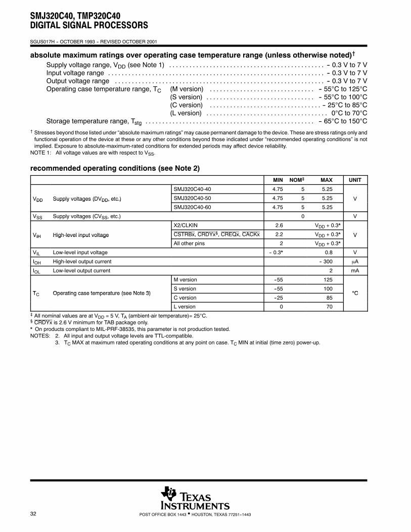
absolute maximum ratings over operating case temperature range (unless otherwise noted)†
Supply voltage range, VDD (see Note 1) -- 0.3 V to 7 V. . . . . . . . . . . . . . . . . . . . . . . . . . . . . . . . . . . . . . . . . . . . . .Input voltage range -- 0.3 V to 7 V. . . . . . . . . . . . . . . . . . . . . . . . . . . . . . . . . . . . . . . . . . . . . . . . . . . . . . . . . . . . . . . .Output voltage range -- 0.3 V to 7 V. . . . . . . . . . . . . . . . . . . . . . . . . . . . . . . . . . . . . . . . . . . . . . . . . . . . . . . . . . . . . .Operating case temperature range, TC (M version) -- 55°C to 125°C. . . . . . . . . . . . . . . . . . . . . . . . . . . . . . .
(S version) -- 55°C to 100°C. . . . . . . . . . . . . . . . . . . . . . . . . . . . . . . .(C version) -- 25°C to 85°C. . . . . . . . . . . . . . . . . . . . . . . . . . . . . . . . .(L version) 0°C to 70°C. . . . . . . . . . . . . . . . . . . . . . . . . . . . . . . . . . . .
Storage temperature range, Tstg -- 65°C to 150°C. . . . . . . . . . . . . . . . . . . . . . . . . . . . . . . . . . . . . . . . . . . . . . . . . .† Stresses beyond those listed under “absolute maximum ratings” may cause permanent damage to the device. These are stress ratings only andfunctional operation of the device at these or any other conditions beyond those indicated under “recommended operating conditions” is notimplied. Exposure to absolute-maximum-rated conditions for extended periods may affect device reliability.
NOTE 1: All voltage values are with respect to VSS.
recommended operating conditions (see Note 2)
MIN NOM‡ MAX UNIT
SMJ320C40-40 4.75 5 5.25
VDD Supply voltages (DVDD, etc.) SMJ320C40-50 4.75 5 5.25 VVDD Supply voltages (DVDD, etc.)
SMJ320C40-60 4.75 5 5.25
V
VSS Supply voltages (CVSS, etc.) 0 V
X2/CLKIN 2.6 VDD + 0.3*
VIH High-level input voltage CSTRBx, CRDYx§, CREQx, CACKx 2.2 VDD + 0.3* VVIH High level input voltage
All other pins 2 VDD + 0.3*
V
VIL Low-level input voltage -- 0.3* 0.8 V
IOH High-level output current -- 300 μA
IOL Low-level output current 2 mA
M version --55 125
T Operating case temperature (see Note 3)S version --55 100
°CTC Operating case temperature (see Note 3)C version --25 85
°C
L version 0 70‡ All nominal values are at VDD = 5 V, TA (ambient-air temperature)= 25°C.§ CRDYx is 2.6 V minimum for TAB package only.* On products compliant to MIL-PRF-38535, this parameter is not production tested.NOTES: 2. All input and output voltage levels are TTL-compatible.
3. TC MAX at maximum rated operating conditions at any point on case. TC MIN at initial (time zero) power-up.

SMJ320C40, TMP320C40DIGITAL SIGNAL PROCESSORS
SGUS017H -- OCTOBER 1993 -- REVISED OCTOBER 2001
33POST OFFICE BOX 1443 • HOUSTON, TEXAS 77251--1443
electrical characteristics over specified case temperature range (see Note 2)
PARAMETER TEST CONDITIONS MIN TYP† MAX UNIT
VOH High-level output voltage VDD = MIN, IOH = MAX 2.4 3 V
VOL Low-level output voltage VDD = MIN, IOL = MAX 0.3 0.6 V
IZ Three-state current VDD = MAX --20 20 μA
II Input current VI = VSS to VDD --10 10 μA
IIPU Input current (TDI, TCK, and TMS) VI = VSS to VDD (See Note 4) --400 20 μA
IIPD Input current (TRST) VI = VSS to VDD (See Note 4) -- 20 400 μA
IIC Input current, X2/CLKIN only VI = VSS to VDD -- 50 50 μA
ICC Supply currentVDD = MAX, TA = 25°C,f MAX (See Note 5)
320C40-40320C40-50
350 850mAICC Supply current
fx = MAX (See Note 5)320C40-60 350 950
mA
CI Input capacitance 15* pF
CO Output capacitance 15* pF† All nominal values are at VDD = 5 V, TA = 25°C.* On products compliant to MIL-PRF-38535, this parameter is not production tested.NOTES: 2. All input and output voltage levels are TTL-compatible.
4. Pins with internal pullup devices: TDI, TCK, TMS. Pin with internal pulldown device: TRST.5. fx is the input clock frequency. The maximum value (MAX) for the 320C40-40, 320C40-50, and 320C40-60 is 40, 50, and 60 MHz,
respectively.
PARAMETER MEASUREMENT INFORMATION
Tester PinElectronics
VLoad
IOL
CT
IOH
OutputUnderTest
Where: IOL = 2 mA (all outputs)IOH = 300 μA (all outputs)VLoad = 2.15 VCT = 80 pF typical load circuit capacitance.
Figure 5. Test Load Circuit

SMJ320C40, TMP320C40DIGITAL SIGNAL PROCESSORS
SGUS017H -- OCTOBER 1993 -- REVISED OCTOBER 2001
34 POST OFFICE BOX 1443 • HOUSTON, TEXAS 77251--1443
PARAMETER MEASUREMENT INFORMATION
signal transition levels
TTL-level outputs are driven to a minimum logic-high level of 2.4 V and to a maximum logic-low level of 0.6 V.Output transition times are specified as follows:
For a high-to-low transition on a TTL-compatible output signal, the level at which the output is said to be nolonger high is 2 V, and the level at which the output is said to be low is 1 V. For a low-to-high transition, the levelat which the output is said to be no longer low is 1 V, and the level at which the output is said to be high is 2 V.See Figure 6.
0.6 V1 V
2 V2.4 V
Figure 6. TTL-Level Outputs
Transition times for TTL-compatible inputs are specified as follows:
For a high-to-low transition on an input signal, the level at which the input is said to be no longer high is 2 V, andthe level at which the input is said to be low is 0.8 V. For a low-to-high transition on an input signal, the level atwhich the input is said to be no longer low is 0.8 V, and the level at which the input is said to be high is 2 V. SeeFigure 7.
2 V
0.8 V
2.4 V†
0.4 V
† Exceptions: X2CLKIN
VIH = 3.12 V and CSTRBx, CRDYx, CREQx and CACKx VIH = 2.64 V.
Figure 7. TTL-Level Inputs
Timing measurements, excluding TR, TF, and T disable (output going to high impedance or an I/O outputbecoming an input), are referenced from an input trip point of 1.5 V to an output trip point of 2 V. Timingmeasurements from H1 and H3 are referenced from 2 V on the rising or falling edges. TR and TF times arereferenced from 20% below VOH minimum to 20% above VOL maximum. T disable times are referenced froman input trip point of 1.5 V to 0.1 V below VOH (TPHZ) or above VOL (TPLZ). The IOL and IOH load current canbe increased to reduce the RC time constant during TPHZ and TPLZ testing.
SMJ320C40, TMP320C40DIGITAL SIGNAL PROCESSORS
SGUS017H -- OCTOBER 1993 -- REVISED OCTOBER 2001
35POST OFFICE BOX 1443 • HOUSTON, TEXAS 77251--1443
timing parameter symbology
Timing parameter symbols used herein were created in accordance with JEDEC Standard 100-A.To shortenthe symbols, pin names that have both global and local applications generally are represented with (L)immediately preceding the basic signal name [for example, (L)RDY represents both the global term RDY andthe local term LRDY]. Other pin names and related terminology have been abbreviated as follows, unlessotherwise noted:
A (L)A30--(L)A0 or (L)Ax H H1/H3
AE LAE, AE, or (L)AE IACK IACK
ASYNCH asynchronous reset signals IIOF IIOF(3--0) or IIOFx
BYTE byte transfer LOCK LLOCK, LOCK, or (L)LOCK
CA CACK(0--5) or CACKx (L)RDY (L)RDY0, (L)RDY1, or (L)RDYx
CD C(0--5)D7--C(0--5)D0 or CxDx P tc(H)
CE (L)CE0, (L)CE1, or (L)CEx PAGE (L)PAGE0, (L)PAGE1, or (L)PAGEx
CI X2/CLKIN RESET RESET
COMM asynchronous reset signals RW (L)R/W0, (L)R/W1, or (L)R/Wx
CONTROL control signals S (L)STRB0, (L)STRB1, or (L)STRBx
CRDY CRDY(0--5) or CRDYx ST (L)STAT3--(L)STAT0 or (L)STATx
CRQ CREQ(0--5) or CREQx TCK TCK
CS CSTRB(0--5) or CSTRBx TDO TDO
D (L)D31--(L)D0 or (L)Dx TMS TMS/TDI
DE LDE, DE, or (L)DE WORD word transfer

SMJ320C40, TMP320C40DIGITAL SIGNAL PROCESSORS
SGUS017H -- OCTOBER 1993 -- REVISED OCTOBER 2001
36 POST OFFICE BOX 1443 • HOUSTON, TEXAS 77251--1443
timing parameters for X2/CLKIN, H1, H3 (see Figure 8 and Figure 9)
NO320C40-40 320C40-50 320C40-60
UNITNO.MIN MAX MIN MAX MIN MAX
UNIT
1 tf(CI) Fall time, CLKIN 5* 5* 5* ns
2 tw(CIL) Pulse duration, CLKIN low, tc(CI) = min 8.5 7 5 ns
3 tw(CIH) Pulse duration, CLKIN high, tc(CI) = min 8.5 7 5 ns
4 tr(CI) Rise time, CLKIN 5* 5* 5* ns
5 tc(CI) Cycle time, CLKIN 25 242.5 20 242.5 16.67 242.5 ns
6 tf(H) Fall time, H1/H3 3* 3* 3* ns
7 tw(HL) Pulse duration, H1/H3 low tc(Cl)--6 tc(Cl)+6 tc(Cl)--6 tc(Cl)+6 tc(Cl)--6 tc(Cl)+6 ns
8 tw(HH) Pulse duration, H1/H3 high tc(Cl)--6 tc(Cl)+6 tc(Cl)--6 tc(Cl)+6 tc(Cl)--6 tc(Cl)+6 ns
9 tr(H) Rise time, H1/H3 4* 4* 4* ns
9.1 td(HL-HH)Delay time, from H1 low to H3 high orfrom H3 low to H1 high
--1 4 --1 4 --1 4 ns
10 tc(H) Cycle time, H1/H3 50 485 40 485 33.3 485 ns
* On products compliant to MIL-PRF-38535, this parameter is not production tested.
1
4
X2/CLKIN
5
23
Figure 8. X2/CLKIN Timing
H3
H1
69
9.1
9.1
69
10
8
7
7
8
10
Figure 9. H1/H3 Timings

SMJ320C40, TMP320C40DIGITAL SIGNAL PROCESSORS
SGUS017H -- OCTOBER 1993 -- REVISED OCTOBER 2001
37POST OFFICE BOX 1443 • HOUSTON, TEXAS 77251--1443
timing parameters for a memory read/write [(L)STRBx = 0] (see Note 6, Figure 10, and Figure 11)
NO320C40-40 320C40-50 320C40-60
UNITNO.MIN MAX MIN MAX MIN MAX
UNIT
1 td(H1L-SL) Delay time, H1 low to (L)STRBx low 0* 10 0* 10 0* 8 ns
2 td(H1L-SH) Delay time, H1 low to (L)STRBx high 0* 10 0* 10 0* 8 ns
3 td(H1H-RWL) Delay time, H1 high to (L)R/Wx low 0* 9 0* 9 0* 8 ns
4 td(H1L-A) Delay time, H1 low to (L)Ax valid 0* 10 0* 9 0* 8 ns
5 tsu(D-H1L)R Setup time, (L)Dx valid before H1 low (read) 15 10 9 ns
6 th(H1L-D)R Hold time, (L)Dx after H1 low (read) 0 0 0 ns
7 tsu[(L)RDY-H1L] Setup time, (L)RDYx valid before H1 low 25 20 18* ns
8 th[H1L-(L)RDY] Hold time, (L)RDYx after H1 low 0 0 0 ns
8.1 td(H1L-ST) Delay time, H1 low to (L)STAT3--(L)STAT0 valid 10 10 8 ns
9 td(H1H-RWH)W Delay time, H1 high to (L)R/Wx high (write) 9 9 0* 8 ns
10 tv(H1L-D)W Valid time, (L)Dx after H1 low (write) 16 16 13 ns
11 th(H1H-D)W Hold time, (L)Dx after H1 high (write) 0 0 0 ns
12 td(H1H-A)Delay time, H1 high to address valid on back-to-backwrite cycles
13 13 8 ns
* On products compliant to MIL-PRF-38535, this parameter is not production tested.NOTE 6: For consecutive reads, (L)R/Wx stays high and (L)STRBx stays low.
6
H3
H1
(L)R/Wx
(L)Ax
(L)Dx
(L)RDYx
(L)STRBx
(L)STAT3--(L)STAT0
53
1 2
4
87
8.1
Figure 10. Memory-Read-Cycle Timing [(L)STRBx = 0]

SMJ320C40, TMP320C40DIGITAL SIGNAL PROCESSORS
SGUS017H -- OCTOBER 1993 -- REVISED OCTOBER 2001
38 POST OFFICE BOX 1443 • HOUSTON, TEXAS 77251--1443
PARAMETER MEASUREMENT INFORMATION
1
(L)RDYx
(L)Dx
(L)Ax
(L)R/Wx
(L)STRBx
H1
H3
9
11
12
8
10
4
(L)STAT3--(L)STAT0
2
3
7
Figure 11. Memory-Write-Cycle Timing [(L)STRBx = 0]

SMJ320C40, TMP320C40DIGITAL SIGNAL PROCESSORS
SGUS017H -- OCTOBER 1993 -- REVISED OCTOBER 2001
39POST OFFICE BOX 1443 • HOUSTON, TEXAS 77251--1443
(L)DE, (L)AE, and (L)CEx enable timings (see Figure 12)
NO.
320C40-40320C40-50 320C40-60
UNITNO.MIN* MAX MIN* MAX
UNIT
1 td(DEH-DZ) Delay time, (L)DE high to (L)D0--(L)D31 in the high-impedance state 0 15* 0 15* ns
2 td(DEL-DV) Delay time, (L)DE low to (L)D0--(L)D31 valid 0 22 0 16 ns
3 td(AEH-AZ) Delay time, (L)AE high to (L)A0--(L)A30 in the high-impedance state 0 15* 0 15* ns
4 td(AEL-AV) Delay time, (L)AE low to (L)A0--(L)A30 valid 0 21 0 16 ns
5 td(CEH-RWZ) Delay time, (L)CEx high to (L)R/W0, (L)R/W1 in the high-impedance state 0 15* 0 15* ns
6 td(CEL-RWV) Delay time, (L)CEx low to (L)R/W0, (L)R/W1 valid 0 21 0 16 ns
7 td(CEH-SZ)Delay time, (L)CEx high to (L)STRB0, (L)STRB1 in the high-impedancestate
0 15* 0 15* ns
8 td(CEL-SV) Delay time, (L)CEx low to (L)STRB0, (L)STRB1 valid 0 21 0 16 ns
9 td(CEH-PAGEZ)Delay time, (L)CEx high to (L)PAGE0, (L)PAGE1 in the high-impedancestate
0 15* 0 15* ns
10 td(CEL-PAGEV) Delay time, (L)CEx low to (L)PAGE0, (L)PAGE1 valid 0 21 0 16 ns
* On products compliant to MIL-PRF-38535, this parameter is not production tested.
(L)DE
(L)D31--(L)D0
(L)AE
(L)A30--(L)A0
(L)CE0, (L)CE1
(L)R/W0, (L)R/W1
(L)STRB0, (L)STRB1
(L)PAGE0, (L)PAGE1
1 2
3 4
Hi-Z
5 6
Hi-Z
7 8
Hi-Z
9 10
Hi-Z
Hi-Z
Figure 12. (L)DE, (L)AE, and (L)CEx Enable Timings
SMJ320C40, TMP320C40DIGITAL SIGNAL PROCESSORS
SGUS017H -- OCTOBER 1993 -- REVISED OCTOBER 2001
40 POST OFFICE BOX 1443 • HOUSTON, TEXAS 77251--1443
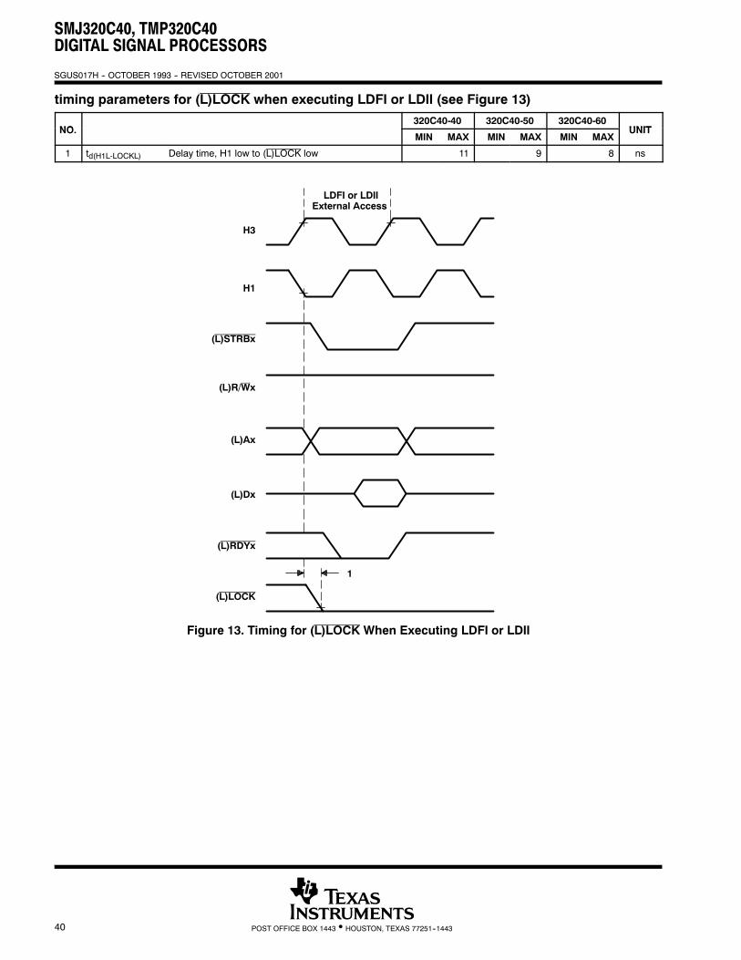
timing parameters for (L)LOCK when executing LDFI or LDII (see Figure 13)
NO320C40-40 320C40-50 320C40-60
UNITNO.MIN MAX MIN MAX MIN MAX
UNIT
1 td(H1L-LOCKL) Delay time, H1 low to (L)LOCK low 11 9 8 ns
H3
H1
(L)STRBx
(L)R/Wx
(L)Ax
(L)Dx
(L)RDYx
(L)LOCK
1
LDFI or LDIIExternal Access
Figure 13. Timing for (L)LOCK When Executing LDFI or LDII

SMJ320C40, TMP320C40DIGITAL SIGNAL PROCESSORS
SGUS017H -- OCTOBER 1993 -- REVISED OCTOBER 2001
41POST OFFICE BOX 1443 • HOUSTON, TEXAS 77251--1443
timing parameters for (L)LOCK when executing STFI or STII (see Figure 14)
NO PARAMETER320C40-40 320C40-50 320C40-60
UNITNO. PARAMETERMIN MAX MIN MAX MIN MAX
UNIT
1 td(H1L-LOCKH) Delay time, H1 low to (L)LOCK high 11 9 8 ns
H3
H1
(L)STRBx
(L)R/Wx
(L)Ax
(L)Dx
(L)RDYx
(L)LOCK
1
STFI or STIIExternal Access
Figure 14. Timing for (L)LOCK When Executing STFI or STII
SMJ320C40, TMP320C40DIGITAL SIGNAL PROCESSORS
SGUS017H -- OCTOBER 1993 -- REVISED OCTOBER 2001
42 POST OFFICE BOX 1443 • HOUSTON, TEXAS 77251--1443
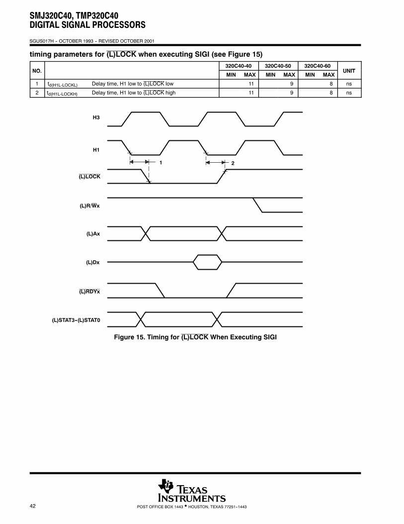
timing parameters for (L)LOCK when executing SIGI (see Figure 15)
NO320C40-40 320C40-50 320C40-60
UNITNO.MIN MAX MIN MAX MIN MAX
UNIT
1 td(H1L-LOCKL) Delay time, H1 low to (L)LOCK low 11 9 8 ns
2 td(H1L-LOCKH) Delay time, H1 low to (L)LOCK high 11 9 8 ns
1
H3
H1
(L)R/Wx
(L)Ax
(L)Dx
(L)RDYx
(L)LOCK
(L)STAT3--(L)STAT0
2
Figure 15. Timing for (L)LOCK When Executing SIGI
SMJ320C40, TMP320C40DIGITAL SIGNAL PROCESSORS
SGUS017H -- OCTOBER 1993 -- REVISED OCTOBER 2001
43POST OFFICE BOX 1443 • HOUSTON, TEXAS 77251--1443
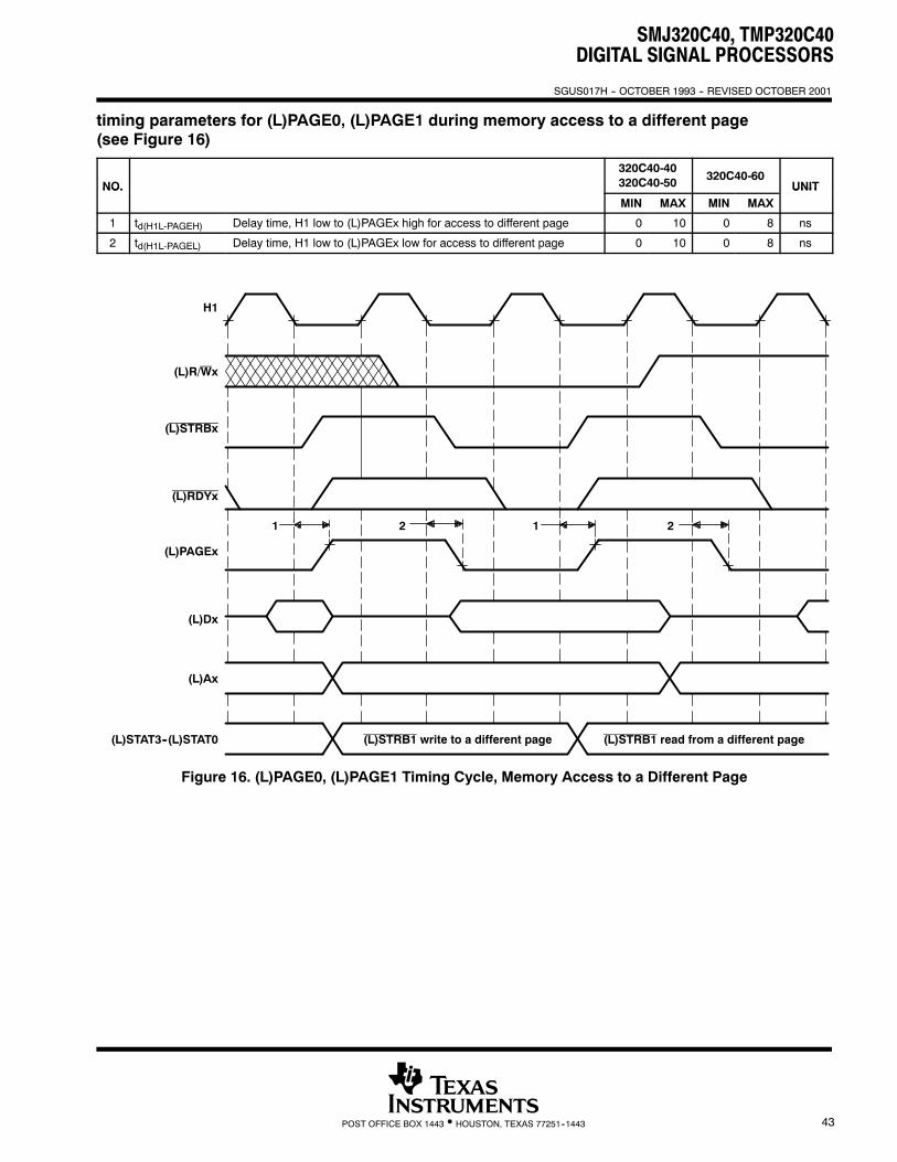
timing parameters for (L)PAGE0, (L)PAGE1 during memory access to a different page(see Figure 16)
NO.
320C40-40320C40-50 320C40-60
UNITNO.MIN MAX MIN MAX
UNIT
1 td(H1L-PAGEH) Delay time, H1 low to (L)PAGEx high for access to different page 0 10 0 8 ns
2 td(H1L-PAGEL) Delay time, H1 low to (L)PAGEx low for access to different page 0 10 0 8 ns
(L)STRB1 read from a different page
(L)Ax
(L)Dx
(L)PAGEx
(L)RDYx
(L)STRBx
(L)R/Wx
H1
1 1 22
(L)STRB1 write to a different page(L)STAT3--(L)STAT0
Figure 16. (L)PAGE0, (L)PAGE1 Timing Cycle, Memory Access to a Different Page
SMJ320C40, TMP320C40DIGITAL SIGNAL PROCESSORS
SGUS017H -- OCTOBER 1993 -- REVISED OCTOBER 2001
44 POST OFFICE BOX 1443 • HOUSTON, TEXAS 77251--1443
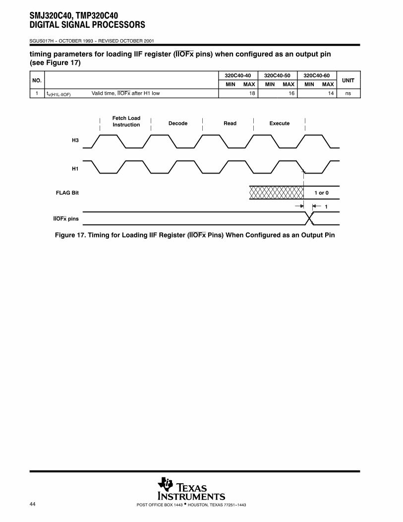
timing parameters for loading IIF register (IIOFx pins) when configured as an output pin(see Figure 17)
NO320C40-40 320C40-50 320C40-60
UNITNO.MIN MAX MIN MAX MIN MAX
UNIT
1 tv(H1L-IIOF) Valid time, IIOFx after H1 low 18 16 14 ns
Fetch LoadInstruction Decode Read Execute
H3
H1
FLAG Bit
IIOFx pins
1 or 0
1
Figure 17. Timing for Loading IIF Register (IIOFx Pins) When Configured as an Output Pin
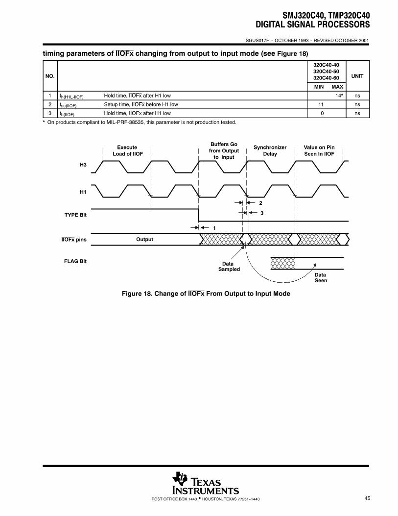
SMJ320C40, TMP320C40DIGITAL SIGNAL PROCESSORS
SGUS017H -- OCTOBER 1993 -- REVISED OCTOBER 2001
45POST OFFICE BOX 1443 • HOUSTON, TEXAS 77251--1443
timing parameters of IIOFx changing from output to input mode (see Figure 18)
NO.
320C40-40320C40-50320C40-60 UNIT
MIN MAX
1 th(H1L-IIOF) Hold time, IIOFx after H1 low 14* ns
2 tsu(IIOF) Setup time, IIOFx before H1 low 11 ns
3 th(IIOF) Hold time, IIOFx after H1 low 0 ns
* On products compliant to MIL-PRF-38535, this parameter is not production tested.
ExecuteLoad of IIOF
Buffers Gofrom Outputto Input
SynchronizerDelay
Value on PinSeen In IIOF
H3
H1
IIOFx pins
FLAG Bit
TYPE Bit
1
2
3
DataSampled
DataSeen
Output
Figure 18. Change of IIOFx From Output to Input Mode

SMJ320C40, TMP320C40DIGITAL SIGNAL PROCESSORS
SGUS017H -- OCTOBER 1993 -- REVISED OCTOBER 2001
46 POST OFFICE BOX 1443 • HOUSTON, TEXAS 77251--1443
timing parameters of IIOFx changing from input to output mode (see Figure 19)
NO.
320C40-40320C40-50 320C40-60
UNITNO.MIN MAX MIN MAX
UNIT
1 td(H1L-IFIO) Delay time, H1 low to IIOFx switching from input to output 16 14 ns
Execution ofLoad of IIOF
1
H3
H1
TYPE Bit
IIOFx pins
Figure 19. Change of IIOFx From Input to Output Mode
timing parameters for RESET (see Figure 20)
NO320C40-40 320C40-50 320C40-60
UNITNO.MIN MAX MIN MAX MIN MAX
UNIT
1 tsu(RESET-CIL) Setup time, RESET before CLKIN low 11 tc(CI) 11 tc(Cl)* 11 tc(Cl)* ns
2.1 td(CIH-H1H) Delay time, CLKIN high to H1 high 2 12 2 10 2 10 ns
2.2 td(CIH-H1L) Delay time, CLKIN high to H1 low 2 12 2 10 2 10 ns
3 tsu(RESETH-H1L)Setup time, RESET high before H1 low andafter ten H1 clock cycles
13 13 13 ns
4.1 td(CIH-H3L) Delay time, CLKIN high to H3 low 2 12 2 10 2 10 ns
4.2 td(CIH-H3H) Delay time, CLKIN high to H3 high 2 12 2 10 2 11 ns
5 tdis(H1H-DZ)Disable time, H1 high to (L)Dx inhigh-impedance state
13* 13* 13* ns
6 tdis(H3H-AZ)Disable time, H3 high to (L)Ax inhigh-impedance state
9* 9* 9* ns
7 td(H3H-CONTROLH)Delay time, H3 high to control signals high[low for (L)PAGEx]
9* 9* 9* ns
8 td(H1H-IACKH) Delay time, H1 high to IACK high 9* 9* 9* ns
9 tdis(RESETL-ASYNCHZ)Disable time, RESET low to asynchronousreset signals in the high-impedance state
21* 21* 21* ns
10 td(RESETH-COMMH)Delay time, RESET high to asynchronous resetsignals high
15* 15* 15* ns
* On products compliant to MIL-PRF-38535, this parameter is not production tested.

SMJ320C40, TMP320C40DIGITAL SIGNAL PROCESSORS
SGUS017H -- OCTOBER 1993 -- REVISED OCTOBER 2001
POST OFFICE BOX 1443 HOUSTON, TEXAS 77251--1443• 47
PARAMETERMEASUREMENTINFORMATION
(L)PAGE0--(L)PAGE1
(see
NoteC)
ControlS
ignals
(see
NoteC)
(L)Dx
(see
NoteA)
RESET
(see
NotesEandF)
1
2.1
4.1
6 7
8
3
2.2
4.2
ControlSignals
7
X2/CLKIN H1
H3
(L)Ax
(see
NoteB)
IACK
AsynchronousReset
Signals(see
NoteD)
AsynchronousReset
Signals(see
NoteE)
TenH1Clock
Cycles
5
9 910
Hi-Z
Hi-Z
Hi-Z
Hi-Z
NOTES:A.Inthisfigure,(L)Dxincludes
D31--D
0,LD
31--D
0,andCxD
7--C
xD0.
B.(L)Axincludes
A30--A0andLA
30--LA0.
C.ControlsignalsLS
TRB0 ,LS
TRB1,STRB0,STRB1,(L)STAT3--(L)STAT0,(L)LOCK,(L)R/W
0,and(L)R/W
1go
high
while(L)PAGE0and(L)PAGE1go
low.
D.Asynchronousresetsignalsthatgo
intohigh
impedanceafterR
ESETgoes
lowincludeTCLK
0,TCLK
1,IIO
F3--IIOF0,andthecommunication-portcontrolsignals
CREQx ,CACKy,CSTRBy,andCRDYx(wherex=0,1,or2,andy=3,4,or5).(Atreset,ports0,1,and2becomeoutputs,andports3,4,and5becomeinputs.)
E.Asynchronousresetsignalsthatgo
toahigh-logiclevelafterRESETgoes
lowincludeCREQy,CACKx,CSTRBx,andCRDYy(wherex=0,1,or2,andy=3,
4,or5).
F.RESETisan
asynchronous
inputand
canbe
asserted
atanypointduringaclockcycle.Ifthespecified
timings
aremet,the
exactsequenceshow
nwilloccur;
otherwise,an
additionaldelay
ofoneclockcyclecanoccur. Figure
20.R
ESETTiming
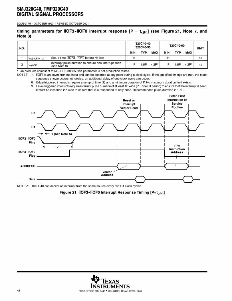
SMJ320C40, TMP320C40DIGITAL SIGNAL PROCESSORS
SGUS017H -- OCTOBER 1993 -- REVISED OCTOBER 2001
48 POST OFFICE BOX 1443 • HOUSTON, TEXAS 77251--1443
timing parameters for IIOF3--IIOF0 interrupt response [P = tc(H)] (see Figure 21, Note 7, andNote 8)
NO.
’320C40-40’320C40-50 ’320C40-60
UNITNO.MIN TYP MAX MIN TYP MAX
UNIT
1 tsu(IIOF-H1L) Setup time, IIOF3--IIOF0 before H1 low 11 11* ns
2 tw(IIOF)Interrupt pulse duration to ensure one interrupt seen(see Note 9) P 1.5P < 2P* P 1.5P < 2P* ns
* On products compliant to MIL-PRF-38535, this parameter is not production tested.NOTES: 7. IIOFx is an asynchronous input and can be asserted at any point during a clock cycle. If the specified timings are met, the exact
sequence shown occurs; otherwise, an additional delay of one clock cycle can occur.8. Edge-triggered interrupts require a setup of time (1) and a minimum duration of P. No maximum duration limit exists.9. Level-triggered interrupts require interrupt pulse duration of at least 1P wide (P = one H1 period) to ensure that the interrupt is seen.
It must be less than 2P wide to ensure that it is responded to only once. Recommended pulse duration is 1.5P.
Reset orInterrupt
Vector Read
Fetch FirstInstruction of
ServiceRoutine
H3
H1
IIOF3--IIOF0Pins
IIOF3--IIOF0Flag
ADDRESS
Data
VectorAddress
FirstInstructionAddress
1 (See Note A)
2
NOTE A: The ’C40 can accept an interrupt from the same source every two H1 clock cycles.
Figure 21. IIOF3--IIOF0 Interrupt Response Timing [P=tc(H)]
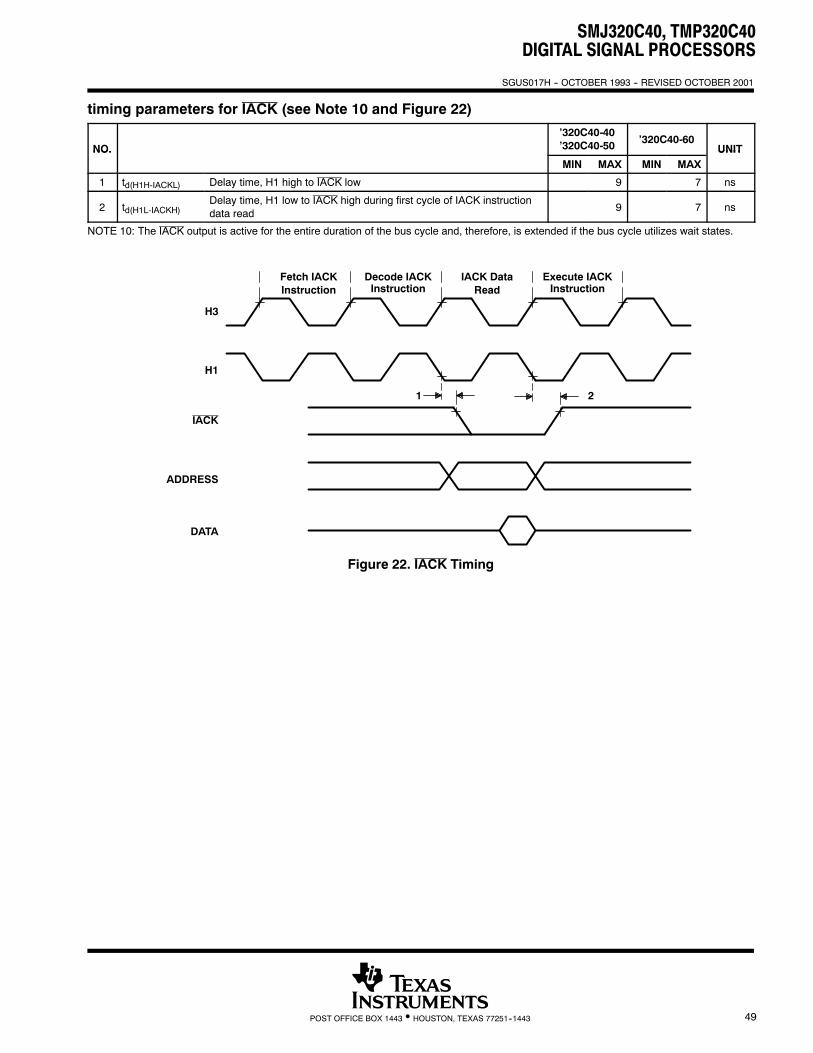
SMJ320C40, TMP320C40DIGITAL SIGNAL PROCESSORS
SGUS017H -- OCTOBER 1993 -- REVISED OCTOBER 2001
49POST OFFICE BOX 1443 • HOUSTON, TEXAS 77251--1443
timing parameters for IACK (see Note 10 and Figure 22)
NO.
’320C40-40’320C40-50 ’320C40-60
UNITNO.MIN MAX MIN MAX
UNIT
1 td(H1H-IACKL) Delay time, H1 high to IACK low 9 7 ns
2 td(H1L-IACKH)Delay time, H1 low to IACK high during first cycle of IACK instructiondata read
9 7 ns
NOTE 10: The IACK output is active for the entire duration of the bus cycle and, therefore, is extended if the bus cycle utilizes wait states.
H3
H1
IACK
ADDRESS
DATA
1 2
Fetch IACKInstruction
IACK DataRead
Decode IACKInstruction
Execute IACKInstruction
Figure 22. IACK Timing

SMJ320C40, TMP320C40DIGITAL SIGNAL PROCESSORS
SGUS017H -- OCTOBER 1993 -- REVISED OCTOBER 2001
50 POST OFFICE BOX 1443 • HOUSTON, TEXAS 77251--1443
communication-port word-transfer cycle timing [P=tc(H)] (see Note 11 and Figure 23)
NO.
’320C40-40†
’320C40-50†
’320C40-60† UNIT
MIN MAX
1 tc(WORD)‡ Cycle time, word transfer (4 bytes = 1 word) 1.5P+7 2.5P+17 ns
2 td(CRDYL-CSL)W* Delay time, CRDYx low to CSTRBx low between back-to-back write cycles 1.5P+7 2.5P+28 ns† For these timing values, it is assumed that the SMJ320C40 that is to receive data is ready to receive data.‡ tc(WORD) max = 2.5P + 28 ns + 4(¥) + 3(© + ¨ + £), where boxed numbers refer to the max values for corresponding parameters in thecommunication-port byte timing table on the next page (for example,¥ means the value under max for parameter 6 in the table ---- a value of10 ns). This timing assumes that two ’C40s are connected.
* On products compliant to MIL-PRF-38535, this parameter is not production tested.NOTE 11: These timings apply only to two communicating ’C4xs. When a non-’C4x device communicates with a ’C40, timings can be longer. No
restriction exists in this case on how slow the transfer could be except when using early silicon (’C40 P6 1.x or 2.x). See the CSTRBwidth restriction in Section 8.9.1 of the TMS320C4x User’s Guide (literature number SPRU063).
CREQx
CACKx
CSTRBx
CxD7--CxD0
CRDYx
1
2
Undef.B0 B1 B2 B3 B0 (see Note B)
= when signal is an input (clear = when signal is an output)
NOTES: A. For correct operation during token exchange, the two communicating SMJ320C40s must have CLKIN frequencies within a factorof 2 of each other (in other words, at most, one of the SMJ320C40s can be twice as fast as the other).
B. Begins byte 0 of the next word
Figure 23. Communication-Port Word-Transfer-Cycle Timing [P=tc(H)]

SMJ320C40, TMP320C40DIGITAL SIGNAL PROCESSORS
SGUS017H -- OCTOBER 1993 -- REVISED OCTOBER 2001
51POST OFFICE BOX 1443 • HOUSTON, TEXAS 77251--1443
communication-port byte timing parameters (write and read) (see Note 12 and Figure 24)
NO.
’320C40-40’320C40-50’320C40-60 UNIT
MIN MAX
1 tsu(CD-CSL)W Setup time, CxDx data valid before CSTRBx low (write) 2 ns
2 td(CRDYL-CSH)W Delay time, CRDYx low to CSTRBx high (write) 0* 12 ns
3 th(CRDYL-CD)W Hold time, CxDx after CRDYx low (write) 1 ns
4 td(CRDYH-CSL)W Delay time, CRDYx high to CSTRBx low for subsequent bytes (write) 0* 12 ns
5 tc(BYTE)† Cycle time, byte transfer 44 ns
6 td(CSL-CRDYL)R Delay time, CSTRBx low to CRDYx low (read) 0* 10 ns
7 tsu(CSH-CD)R Setup time, CxDx valid after CSTRBx high (read) 0 ns
8 th(CRDYL-CD)R Hold time, CxDx valid after CRDYx low (read) 2 ns
9 td(CSH-CRDYH)R Delay time, CSTRBx high to CRDYx high (read) 0* 10 ns† tc(BYTE) max = (© +£ +¥ +¨) where boxed numbers refer to the max values for corresponding parameters in the above table (for example,¥ means the value under max for parameter 6 in the table — a value of 10 ns). This assumes that two ’C40s are connected.
* On products compliant to MIL-PRF-38535, this parameter is not production tested.NOTE 12: Communication port timing does not include line length delay.
CREQx
CACKx
CSTRBx
CxDx
CRDYx
(a) WRITE TIMING (b) READ TIMING
1
4
7
6
8
2
3
5
9
5
= when signal is an input (clear = when signal is an output)
Valid Data Valid
Figure 24. Communication-Port Byte Timing (Write and Read)

SMJ320C40, TMP320C40DIGITAL SIGNAL PROCESSORS
SGUS017H -- OCTOBER 1993 -- REVISED OCTOBER 2001
52 POST OFFICE BOX 1443 • HOUSTON, TEXAS 77251--1443
timing parameters for communication-token transfer sequence, input to an output port [P = tc(H)]†(see Figure 25)
NO.
’320C40-40*’320C40-50*’320C40-60* UNIT
MIN MAX
1† td(CAL-CS)T Delay time, CACKx low to CSTRBx change from input to a high-level output 0.5P+ 6 1.5P+ 22 ns
2† td(CAL-CRQH)TDelay time, CACKx low to start of CREQx going high for token-requestacknowledge
P + 5 2P + 26 ns
3 td(CRQH-CRQ)T Delay time, start of CREQx going high to CREQx change from output to an input 0.5P -- 5 0.5P+ 13 ns
4 td(CRQH-CA)TDelay time, start of CREQx going high to CACKx change from an input to anoutput level high
0.5P -- 5 0.5P+13 ns
4.1 td(CRQH-CD)TDelay time, start of CREQx going high to CxD7--CxD0 change from inputsdriven to outputs driven
0.5P -- 5 0.5P+13 ns
4.2 td(CRQH-CRDY)TDelay time, start of CREQx going high to CRDYx change from an output to aninput
0.5P -- 5 0.5P+13 ns
5 td(CRQH-CSL)TDelay time, start of CREQx going high to CSTRBx low for start of word transferout
1.5P -- 8 1.5P+ 9 ns
6 td(CRDYL-CSL)T Delay time, CRDYx low at end of word input to CSTRBx low for word output 3.5P+12 5.5P+ 48 ns† These timing parameters result from synchronizer delays and are referenced from the falling edge of H1. The inputs (that cause the output-signalpins to change values) are sampled on H1 falling. The minimum delay occurs when the input condition occurs just before H1 falling, and themaximum delay occurs when the input condition occurs just after H1 falling.
* On products compliant to MIL-PRF-38535, this parameter is not production tested.
CREQx
CACKx
CSTRBx
CxD7--CxD0
CRDYx
= when signal is an input (clear = when signal is an output)
6
3
4
1
4.1
4.2
Valid Data Out
2
5
NOTE A: Before the token exchange, CREQx and CRDYx are output signals asserted by the SMJ320C40 that is receiving data. CACKx,CSTRBx, and CxD7--CxD0 are input signals asserted by the device sending data to the ’C40; these are asynchronous with respect tothe H1 clock of the receiving SMJ320C40. After token exchange, CACKx, CSTRBx, and CxD7--CxD0 become output signals, andCREQx and CRDYx become inputs.
Figure 25. Communication-Token Transfer Sequence, Input to an Output Port [P=tc(H)]
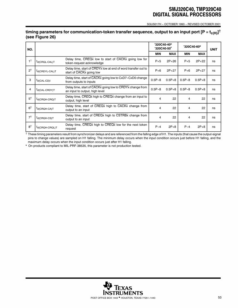
SMJ320C40, TMP320C40DIGITAL SIGNAL PROCESSORS
SGUS017H -- OCTOBER 1993 -- REVISED OCTOBER 2001
53POST OFFICE BOX 1443 • HOUSTON, TEXAS 77251--1443
timing parameters for communication-token transfer sequence, output to an input port [P = tc(H)]†(see Figure 26)
NO.
’320C40-40*’320C40-50* ’320C40-60*
UNITNO.MIN MAX MIN MAX
UNIT
1† td(CRQL-CAL)TDelay time, CREQx low to start of CACKx going low fortoken-request acknowledge
P+5 2P+26 P+5 2P+22 ns
2† td(CRDYL-CAL)TDelay time, start of CRDYx low at end of word transfer out tostart of CACKx going low
P+6 2P+27 P+6 2P+27 ns
3 td(CAL-CD)IDelay time, start of CACKx going low to CxD7--CxD0 changefrom outputs to inputs
0.5P--8 0.5P+8 0.5P--8 0.5P+8 ns
4 td(CAL-CRDY)TDelay time, start of CACKx going low to CRDYx change froman input to output, high level
0.5P--8 0.5P+8 0.5P--8 0.5P+8 ns
5† td(CRQH-CRQ)TDelay time, CREQx high to CREQx change from an input tooutput, high level
4 22 4 22 ns
6† td(CRQH-CA)TDelay time, start of CREQx high to CACKx change fromoutput to an input
4 22 4 22 ns
7† td(CRQH-CS)TDelay time, start of CREQx high to CSTRBx change fromoutput to an input
4 22 4 22 ns
8† td(CRQH-CRQL)TDelay time, CREQx high to CREQx low for the next tokenrequest
P--4 2P+8 P--4 2P+8 ns
† These timing parameters result from synchronizer delays and are referenced from the falling edge of H1. The inputs (that cause the output-signalpins to change values) are sampled on H1 falling. The minimum delay occurs when the input condition occurs just before H1 falling, and themaximum delay occurs when the input condition occurs just after H1 falling.
* On products compliant to MIL-PRF-38535, this parameter is not production tested.

SMJ320C40, TMP320C40DIGITAL SIGNAL PROCESSORS
SGUS017H -- OCTOBER 1993 -- REVISED OCTOBER 2001
54 POST OFFICE BOX 1443 • HOUSTON, TEXAS 77251--1443
PARAMETER MEASUREMENT INFORMATION
CREQx
CACKx
CSTRBx
CxD7--CxD0
CRDYx
= when signal is an input (clear = when signal is an output)
Valid data
1 5
6
7
8
3
4
2
Valid data
NOTE A: Before the token exchange, CACKx, CSTRBx, and CxD7--CxD0 are asserted by the ’C40 sending data. CREQx and CRDYx are inputsignals asserted by the ’C40 receiving data and are asynchronous with respect to the H1 clock of the sending ’C40. After tokenexchange, CREQx and CRDYx become outputs, and CSTRBx, CACKx, and CxD7--CxD0 become inputs.
Figure 26. Communication-Token Transfer Sequence, Output to an Input Port [P=tc(H)]
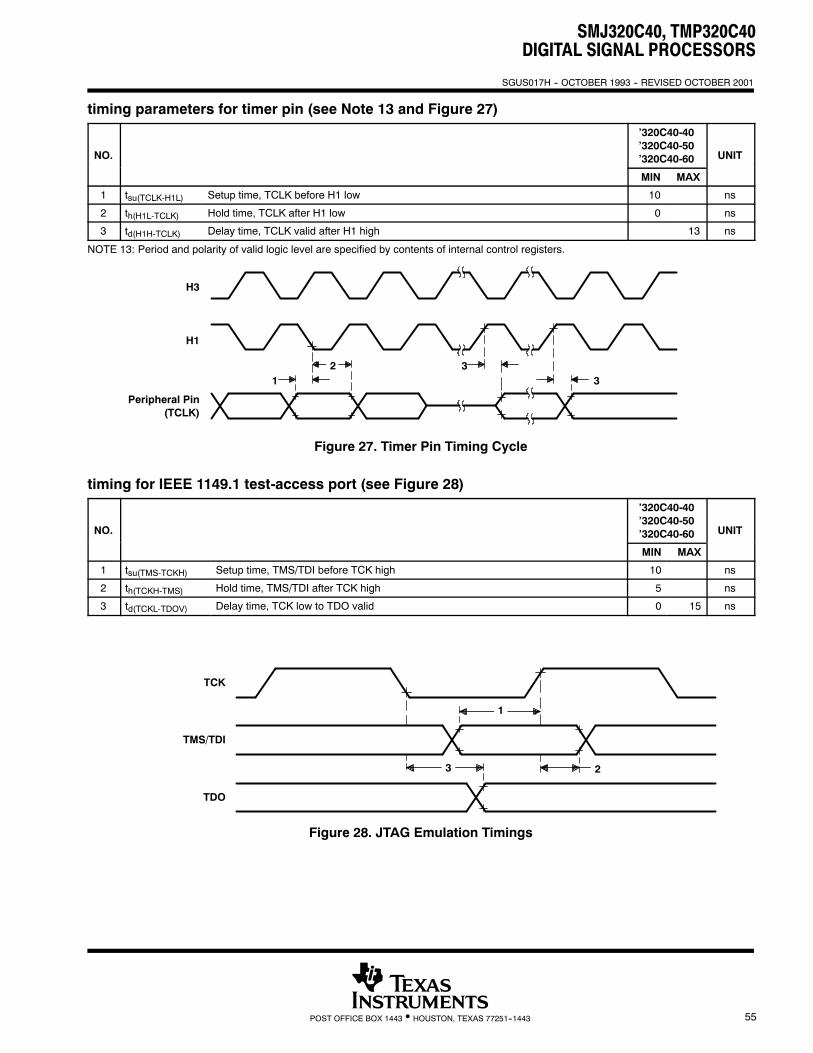
SMJ320C40, TMP320C40DIGITAL SIGNAL PROCESSORS
SGUS017H -- OCTOBER 1993 -- REVISED OCTOBER 2001
55POST OFFICE BOX 1443 • HOUSTON, TEXAS 77251--1443
timing parameters for timer pin (see Note 13 and Figure 27)
NO.
’320C40-40’320C40-50’320C40-60 UNIT
MIN MAX
1 tsu(TCLK-H1L) Setup time, TCLK before H1 low 10 ns
2 th(H1L-TCLK) Hold time, TCLK after H1 low 0 ns
3 td(H1H-TCLK) Delay time, TCLK valid after H1 high 13 ns
NOTE 13: Period and polarity of valid logic level are specified by contents of internal control registers.
33
Peripheral Pin(TCLK)
H1
H3
12
Figure 27. Timer Pin Timing Cycle
timing for IEEE 1149.1 test-access port (see Figure 28)
NO.
’320C40-40’320C40-50’320C40-60 UNIT
MIN MAX
1 tsu(TMS-TCKH) Setup time, TMS/TDI before TCK high 10 ns
2 th(TCKH-TMS) Hold time, TMS/TDI after TCK high 5 ns
3 td(TCKL-TDOV) Delay time, TCK low to TDO valid 0 15 ns
TCK
TMS/TDI
TDO
3 2
1
Figure 28. JTAG Emulation Timings

SMJ320C40, TMP320C40DIGITAL SIGNAL PROCESSORS
SGUS017H -- OCTOBER 1993 -- REVISED OCTOBER 2001
56 POST OFFICE BOX 1443 • HOUSTON, TEXAS 77251--1443
PRODUCT ORDERING INFORMATION
SMJ320C40 standard package ordering information
DEVICETEMPERATURE
RANGEOPERATINGFREQUENCY PACKAGE TYPE
PROCESSINGLEVEL
SMJ320C40GFM40 -- 55°C to 125°C 40 MHz Ceramic 325-pin staggered PGA (GF) QML
SM320C40GFM40 -- 55°C to 125°C 40 MHz Ceramic 325-pin staggered PGA (GF) Standard
SMJ320C40GFM50 -- 55°C to 125°C 50 MHz Ceramic 325-pin staggered PGA QML
SM320C40GFM50 -- 55°C to 125°C 50 MHz Ceramic 325-pin staggered PGA Standard
SMJ320C40HFHM40 -- 55°C to 125°C 40 MHz Ceramic 352-pin quad flatpack (HFH) QML
SM320C40HFHM40 -- 55°C to 125°C 40 MHz Ceramic 352-pin quad flatpack (HFH) Standard
SMJ320C40HFHM50 -- 55°C to 125°C 50 MHz Ceramic 352-pin quad flatpack QML
SM320C40HFHM50 -- 55°C to 125°C 50 MHz Ceramic 352-pin quad flatpack Standard
SMJ320C40GFS60 -- 55°C to 100°C 60 MHz Ceramic 325-pin staggered PGA QML
SM320C40GFS60 -- 55°C to 100°C 60 MHz Ceramic 325-pin staggered PGA Standard
SMJ320C40HFHS60 -- 55°C to 100°C 60 MHz Ceramic 352-pin quad flatpack QML
SM320C40HFHS60 -- 55°C to 100°C 60 MHz Ceramic 352-pin quad flatpack Standard
SMJ320C40 TAB ordering information†
DEVICETEMPERATURE
RANGEOPERATINGFREQUENCY PACKAGE TYPE
PROCESSINGLEVEL
SMJ320C40TABM40/10 -- 55°C to 125°C 40 MHz 325 ILB/OLB TAB tape (encapsulated) QML
SM320C40TABM40/10 -- 55°C to 125°C 40 MHz 325 ILB/OLB TAB tape (encapsulated) Standard
SMJ320C40TABM50/10 -- 55°C to 125°C 50 MHz 325 ILB/OLB TAB tape (encapsulated) QML
SM320C40TABM50/10 -- 55°C to 125°C 50 MHz 325 ILB/OLB TAB tape (encapsulated) Standard
SM320C40TABS50/10 -- 55°C to 100°C 50 MHz 325 ILB/OLB TAB tape (encapsulated) Standard
TMP320C40TABL50/10 0°C to 70°C 50 MHz 325 ILB/OLB TAB tape (encapsulated)Commercial(No Burn-In)
SM320C40TABC50/10 -- 25°C to 85°C 50 MHz 325 ILB/OLB TAB tape (encapsulated)Commercial(No Burn-In)
SMJ320C40TABS60/10 -- 55°C to 100°C 60 MHz 325 ILB/OLB TAB tape (encapsulated) QML
SM320C40TABS60/10 -- 55°C to 100°C 60 MHz 325 ILB/OLB TAB tape (encapsulated) Standard
TMP320C40TABL60/10 0°C to 70°C 60 MHz 325 ILB/OLB TAB tape (encapsulated)Commercial(No Burn-In)
† /10 indicates solder-dip TAB lead frame.

4040035-2/E 03/97
1.879 (47,73)1.841 (46,76)
SQ
TYP
0.050 (1,27) TYP
0.080 (2,03) TYP
0.150 (3,81)
0.145 (3,68)
0.200 (5,08) DETAIL A
1.717 (43,61)TYP
3533312925 2719 211715131197 23
1.683 (42,75)
ARAN
AJAGAE
AAAC
AL
W
RU
NL
53
GE
AC
1
J
0.120 (3,05)
0.165 (4,19)
0.016 (0,41)0.020 (0,51)
0.040 (1,02)
0.006 (0,152)
0.060 (1,52)
0.026 (0,660)
0.170 (4,32)0.190 (4,83)
0.048 (1,22) DIA 4 Places0.050 (1,27)
0.100 (2,54)
NOTES: A. All linear dimensions are in inches (millimeters).B. This drawing is subject to change without notice.C. Index mark can appear on top or bottom, depending on package vendor.D. Pins are located within 0.010 (0,25) diameter of true position relative to
each other at maximum material condition and within0.030 (0,76) diameter relative to the edge of the ceramic.
E. This package can be hermetically sealed with metal lidsor with ceramic lids using glass frit.
F. The pins can be gold-plated or solder-dipped.G. Package thickness of 0.165 (4,19) / 0.120 (3,05) includes
package body and lid.H. Falls within JEDEC MO-128AK
SMJ320C40, TMP320C40DIGITAL SIGNAL PROCESSORS
SGUS017H -- OCTOBER 1993 -- REVISED OCTOBER 2001
57POST OFFICE BOX 1443 • HOUSTON, TEXAS 77251--1443
MECHANICAL DATAGF (S-CPGA-P325) CERAMIC PIN GRID ARRAY
Thermal ResistanceCharacteristics
Parameter °C/WAir FlowLFPM
RΘJC 1.7 N/A
RΘJA 10.9 0
RΘJA 9.8 200
RΘJA 7.0 400
RΘJA 6.4 600
RΘJA 5.6 800
RΘJA 5.5 1000
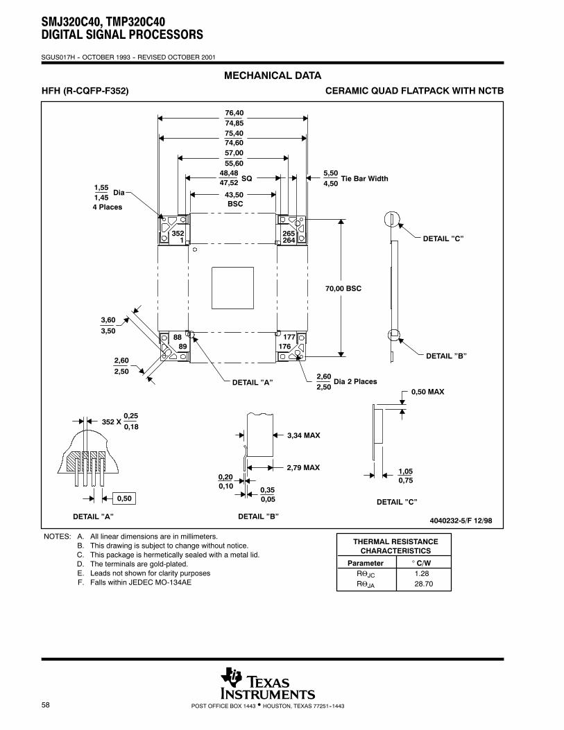
SMJ320C40, TMP320C40DIGITAL SIGNAL PROCESSORS
SGUS017H -- OCTOBER 1993 -- REVISED OCTOBER 2001
58 POST OFFICE BOX 1443 • HOUSTON, TEXAS 77251--1443
MECHANICAL DATAHFH (R-CQFP-F352) CERAMIC QUAD FLATPACK WITH NCTB
5,504,50
265
176177
264
70,00 BSC
Tie Bar Width
DETAIL ”C”
2 Places
0,75
DETAIL ”C”
1,05
Dia2,602,50
3,34 MAX
0,350,05
2,79 MAX
4040232-5/F 12/98
0,50 MAX
DETAIL ”B”
76,4074,85
SQ
74,60
55,6057,00
75,40
48,48
BSC43,50
47,52
352
8889
1
Dia1,454 Places
1,55
3,60
3,50
0,100,20
0,18
0,25352 X
2,50
2,60
DETAIL ”A” DETAIL ”B”
DETAIL ”A”
0,50
NOTES: A. All linear dimensions are in millimeters.B. This drawing is subject to change without notice.C. This package is hermetically sealed with a metal lid.D. The terminals are gold-plated.E. Leads not shown for clarity purposesF. Falls within JEDEC MO-134AE
THERMAL RESISTANCECHARACTERISTICS
Parameter ° C/WRΘJC 1.28RΘJA 28.70
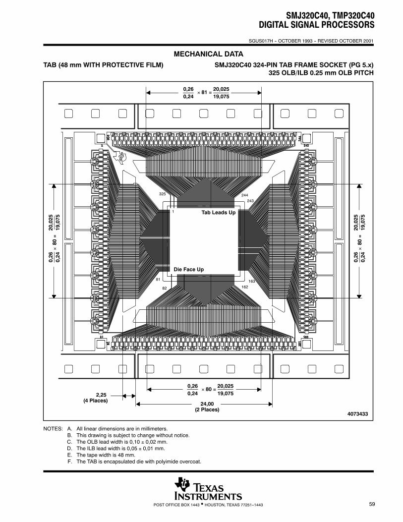
SMJ320C40, TMP320C40DIGITAL SIGNAL PROCESSORS
SGUS017H -- OCTOBER 1993 -- REVISED OCTOBER 2001
59POST OFFICE BOX 1443 • HOUSTON, TEXAS 77251--1443
MECHANICAL DATATAB (48 mm WITH PROTECTIVE FILM) SMJ320C40 324-PIN TAB FRAME SOCKET (PG 5.x)
325 OLB/ILB 0.25 mm OLB PITCH
4073433
2,25(4 Places)
24,00(2 Places)
0,260,24
× 80 =20,02519,075
0,26
0,24
20,025
19,075
80=
×
243244
163162
325
1
82
81
Die Face Up
Tab Leads Up
0,260,24
× 81 =20,02519,075
0,26
0,24
20,025
19,075
80=
×
NOTES: A. All linear dimensions are in millimeters.B. This drawing is subject to change without notice.C. The OLB lead width is 0,10 ± 0,02 mm.D. The ILB lead width is 0,05 ± 0,01 mm.E. The tape width is 48 mm.F. The TAB is encapsulated die with polyimide overcoat.
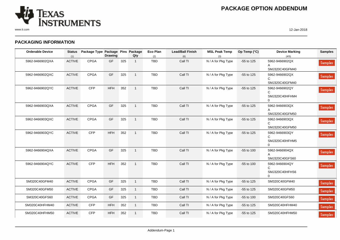
PACKAGE OPTION ADDENDUM
www.ti.com 12-Jan-2018
Addendum-Page 1
PACKAGING INFORMATION
Orderable Device Status(1)
Package Type PackageDrawing
Pins PackageQty
Eco Plan(2)
Lead/Ball Finish(6)
MSL Peak Temp(3)
Op Temp (°C) Device Marking(4/5)
Samples
5962-9466902QXA ACTIVE CPGA GF 325 1 TBD Call TI N / A for Pkg Type -55 to 125 5962-9466902QXASMJ320C40GFM40
5962-9466902QXC ACTIVE CPGA GF 325 1 TBD Call TI N / A for Pkg Type -55 to 125 5962-9466902QXCSMJ320C40GFM40
5962-9466902QYC ACTIVE CFP HFH 352 1 TBD Call TI N / A for Pkg Type -55 to 125 5962-9466902QYCSMJ320C40HFHM40
5962-9466903QXA ACTIVE CPGA GF 325 1 TBD Call TI N / A for Pkg Type -55 to 125 5962-9466903QXASMJ320C40GFM50
5962-9466903QXC ACTIVE CPGA GF 325 1 TBD Call TI N / A for Pkg Type -55 to 125 5962-9466903QXCSMJ320C40GFM50
5962-9466903QYC ACTIVE CFP HFH 352 1 TBD Call TI N / A for Pkg Type -55 to 125 5962-9466903QYCSMJ320C40HFHM50
5962-9466904QXA ACTIVE CPGA GF 325 1 TBD Call TI N / A for Pkg Type -55 to 100 5962-9466904QXASMJ320C40GFS60
5962-9466904QYC ACTIVE CFP HFH 352 1 TBD Call TI N / A for Pkg Type -55 to 100 5962-9466904QYCSMJ320C40HFHS60
SM320C40GFM40 ACTIVE CPGA GF 325 1 TBD Call TI N / A for Pkg Type -55 to 125 SM320C40GFM40
SM320C40GFM50 ACTIVE CPGA GF 325 1 TBD Call TI N / A for Pkg Type -55 to 125 SM320C40GFM50
SM320C40GFS60 ACTIVE CPGA GF 325 1 TBD Call TI N / A for Pkg Type -55 to 100 SM320C40GFS60
SM320C40HFHM40 ACTIVE CFP HFH 352 1 TBD Call TI N / A for Pkg Type -55 to 125 SM320C40HFHM40
SM320C40HFHM50 ACTIVE CFP HFH 352 1 TBD Call TI N / A for Pkg Type -55 to 125 SM320C40HFHM50
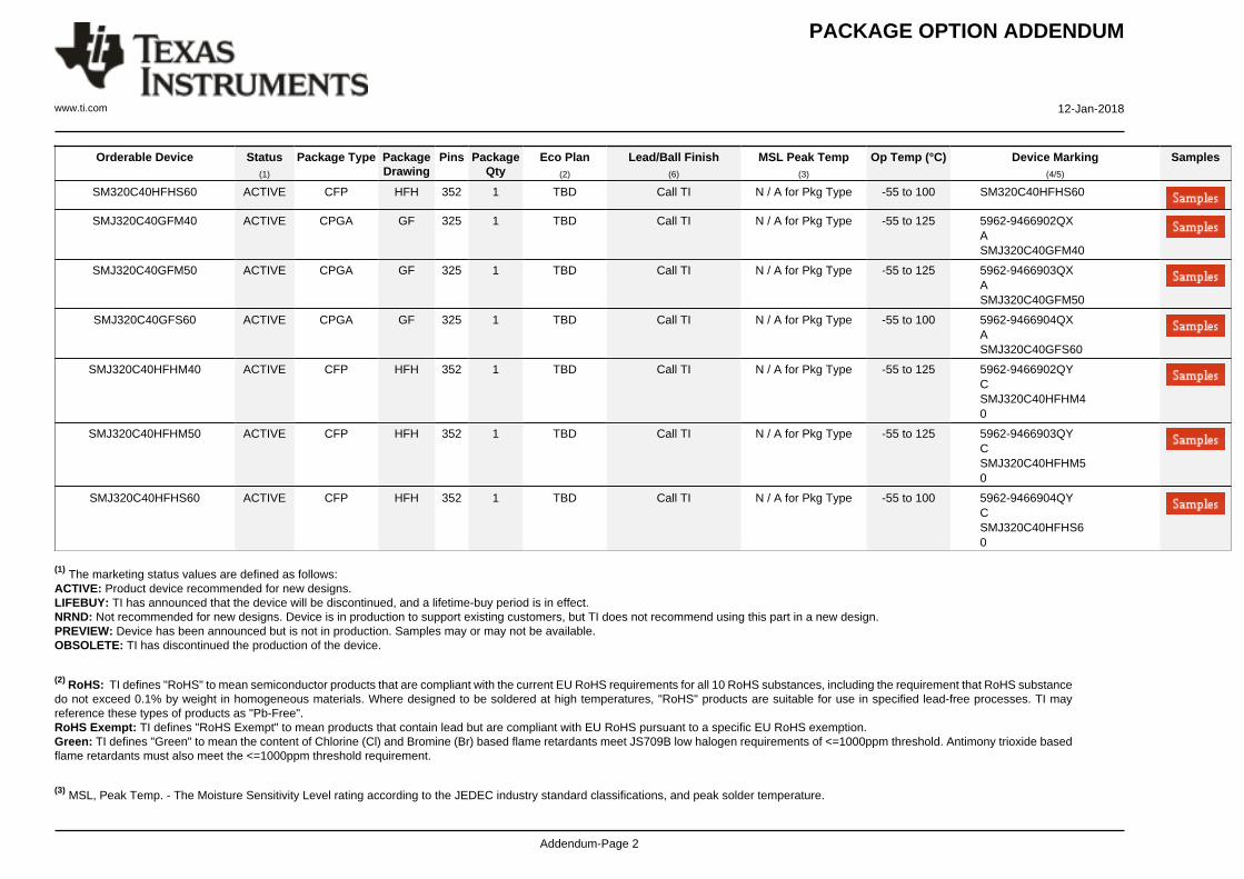
PACKAGE OPTION ADDENDUM
www.ti.com 12-Jan-2018
Addendum-Page 2
Orderable Device Status(1)
Package Type PackageDrawing
Pins PackageQty
Eco Plan(2)
Lead/Ball Finish(6)
MSL Peak Temp(3)
Op Temp (°C) Device Marking(4/5)
Samples
SM320C40HFHS60 ACTIVE CFP HFH 352 1 TBD Call TI N / A for Pkg Type -55 to 100 SM320C40HFHS60
SMJ320C40GFM40 ACTIVE CPGA GF 325 1 TBD Call TI N / A for Pkg Type -55 to 125 5962-9466902QXASMJ320C40GFM40
SMJ320C40GFM50 ACTIVE CPGA GF 325 1 TBD Call TI N / A for Pkg Type -55 to 125 5962-9466903QXASMJ320C40GFM50
SMJ320C40GFS60 ACTIVE CPGA GF 325 1 TBD Call TI N / A for Pkg Type -55 to 100 5962-9466904QXASMJ320C40GFS60
SMJ320C40HFHM40 ACTIVE CFP HFH 352 1 TBD Call TI N / A for Pkg Type -55 to 125 5962-9466902QYCSMJ320C40HFHM40
SMJ320C40HFHM50 ACTIVE CFP HFH 352 1 TBD Call TI N / A for Pkg Type -55 to 125 5962-9466903QYCSMJ320C40HFHM50
SMJ320C40HFHS60 ACTIVE CFP HFH 352 1 TBD Call TI N / A for Pkg Type -55 to 100 5962-9466904QYCSMJ320C40HFHS60
(1) The marketing status values are defined as follows:ACTIVE: Product device recommended for new designs.LIFEBUY: TI has announced that the device will be discontinued, and a lifetime-buy period is in effect.NRND: Not recommended for new designs. Device is in production to support existing customers, but TI does not recommend using this part in a new design.PREVIEW: Device has been announced but is not in production. Samples may or may not be available.OBSOLETE: TI has discontinued the production of the device.
(2) RoHS: TI defines "RoHS" to mean semiconductor products that are compliant with the current EU RoHS requirements for all 10 RoHS substances, including the requirement that RoHS substancedo not exceed 0.1% by weight in homogeneous materials. Where designed to be soldered at high temperatures, "RoHS" products are suitable for use in specified lead-free processes. TI mayreference these types of products as "Pb-Free".RoHS Exempt: TI defines "RoHS Exempt" to mean products that contain lead but are compliant with EU RoHS pursuant to a specific EU RoHS exemption.Green: TI defines "Green" to mean the content of Chlorine (Cl) and Bromine (Br) based flame retardants meet JS709B low halogen requirements of <=1000ppm threshold. Antimony trioxide basedflame retardants must also meet the <=1000ppm threshold requirement.
(3) MSL, Peak Temp. - The Moisture Sensitivity Level rating according to the JEDEC industry standard classifications, and peak solder temperature.

PACKAGE OPTION ADDENDUM
www.ti.com 12-Jan-2018
Addendum-Page 3
(4) There may be additional marking, which relates to the logo, the lot trace code information, or the environmental category on the device.
(5) Multiple Device Markings will be inside parentheses. Only one Device Marking contained in parentheses and separated by a "~" will appear on a device. If a line is indented then it is a continuationof the previous line and the two combined represent the entire Device Marking for that device.
(6) Lead/Ball Finish - Orderable Devices may have multiple material finish options. Finish options are separated by a vertical ruled line. Lead/Ball Finish values may wrap to two lines if the finishvalue exceeds the maximum column width.
Important Information and Disclaimer:The information provided on this page represents TI's knowledge and belief as of the date that it is provided. TI bases its knowledge and belief on informationprovided by third parties, and makes no representation or warranty as to the accuracy of such information. Efforts are underway to better integrate information from third parties. TI has taken andcontinues to take reasonable steps to provide representative and accurate information but may not have conducted destructive testing or chemical analysis on incoming materials and chemicals.TI and TI suppliers consider certain information to be proprietary, and thus CAS numbers and other limited information may not be available for release.
In no event shall TI's liability arising out of such information exceed the total purchase price of the TI part(s) at issue in this document sold by TI to Customer on an annual basis.
OTHER QUALIFIED VERSIONS OF SM320C40, SMJ320C40 :
• Catalog: TMS320C40, TMS320C40
• Military: SMJ320C40
NOTE: Qualified Version Definitions:
• Catalog - TI's standard catalog product
• Military - QML certified for Military and Defense Applications

MECHANICAL DATA
MCPG013F – JANUARY 1995 – REVISED DECEMBER 2001
1POST OFFICE BOX 655303 • DALLAS, TEXAS 75265
GF (S-CPGA-P325) CERAMIC PIN GRID ARRAY
4040035-2/F 11/01
1.879 (47,73)1.841 (46,76)
SQ
TYP
0.050 (1,27) TYP
0.080 (2,03) TYP
0.150 (3,81)
0.145 (3,68)
0.200 (5,08) DETAIL A
1.717 (43,61)TYP
3533312925 2719 211715131197 23
1.683 (42,75)
ARAN
AJAGAE
AAAC
AL
W
RU
NL
53
GE
AC
1
J
0.120 (3,05)
0.165 (4,19)
0.016 (0,41)0.020 (0,51)
0.040 (1,02)
0.006 (0,152)
0.060 (1,52)
0.026 (0,660)
0.170 (4,32)0.190 (4,83)
0.048 (1,22) DIA 4 Places0.050 (1,27)
0.100 (2,54)
A1 Corner
Bottom View
NOTES: A. All linear dimensions are in inches (millimeters).B. This drawing is subject to change without notice.C. Index mark can appear on top or bottom, depending on package vendor.D. Pins are located within 0.010 (0,25) diameter of true position relative to
each other at maximum material condition and within 0.030 (0,76) diameter relative to the edge of the ceramic.
E. This package can be hermetically sealed with metal lids or with ceramic lids using glass frit.F. The pins can be gold-plated or solder-dipped.G. Package thickness of 0.165 (4,19) / 0.120 (3,05) includes package body and lid.H. Falls within JEDEC MO-128AK

MECHANICAL DATA
MCFP029B – JANUARY 1995 – REVISED JUNE 1999
1POST OFFICE BOX 655303 • DALLAS, TEXAS 75265
HFH (R-CQFP-F352) CERAMIC QUAD FLATPACK WITH NCTB
5,504,50
265
176177
264
70,00 BSC
Tie Bar Width
DETAIL ”C”
2 Places
0,75
DETAIL ”C”
1,05
Dia2,602,50
3,34 MAX
0,350,05
2,79 MAX
4040232-5/F 12/98
0,50 MAX
DETAIL ”B”
76,4074,85
SQ
74,60
55,6057,00
75,40
48,48
BSC43,50
47,52
352
8889
1
Dia1,454 Places
1,55
3,60
3,50
0,100,20
0,18
0,25352 X
2,50
2,60
DETAIL ”A” DETAIL ”B”
DETAIL ”A”
0,50
NOTES: A. All linear dimensions are in millimeters.B. This drawing is subject to change without notice.C. This package is hermetically sealed with a metal lid.D. The terminals are gold-plated.E. Leads not shown for clarity purposesF. Falls within JEDEC MO-134AE

IMPORTANT NOTICE
Texas Instruments Incorporated (TI) reserves the right to make corrections, enhancements, improvements and other changes to itssemiconductor products and services per JESD46, latest issue, and to discontinue any product or service per JESD48, latest issue. Buyersshould obtain the latest relevant information before placing orders and should verify that such information is current and complete.TI’s published terms of sale for semiconductor products (http://www.ti.com/sc/docs/stdterms.htm) apply to the sale of packaged integratedcircuit products that TI has qualified and released to market. Additional terms may apply to the use or sale of other types of TI products andservices.Reproduction of significant portions of TI information in TI data sheets is permissible only if reproduction is without alteration and isaccompanied by all associated warranties, conditions, limitations, and notices. TI is not responsible or liable for such reproduceddocumentation. Information of third parties may be subject to additional restrictions. Resale of TI products or services with statementsdifferent from or beyond the parameters stated by TI for that product or service voids all express and any implied warranties for theassociated TI product or service and is an unfair and deceptive business practice. TI is not responsible or liable for any such statements.Buyers and others who are developing systems that incorporate TI products (collectively, “Designers”) understand and agree that Designersremain responsible for using their independent analysis, evaluation and judgment in designing their applications and that Designers havefull and exclusive responsibility to assure the safety of Designers' applications and compliance of their applications (and of all TI productsused in or for Designers’ applications) with all applicable regulations, laws and other applicable requirements. Designer represents that, withrespect to their applications, Designer has all the necessary expertise to create and implement safeguards that (1) anticipate dangerousconsequences of failures, (2) monitor failures and their consequences, and (3) lessen the likelihood of failures that might cause harm andtake appropriate actions. Designer agrees that prior to using or distributing any applications that include TI products, Designer willthoroughly test such applications and the functionality of such TI products as used in such applications.TI’s provision of technical, application or other design advice, quality characterization, reliability data or other services or information,including, but not limited to, reference designs and materials relating to evaluation modules, (collectively, “TI Resources”) are intended toassist designers who are developing applications that incorporate TI products; by downloading, accessing or using TI Resources in anyway, Designer (individually or, if Designer is acting on behalf of a company, Designer’s company) agrees to use any particular TI Resourcesolely for this purpose and subject to the terms of this Notice.TI’s provision of TI Resources does not expand or otherwise alter TI’s applicable published warranties or warranty disclaimers for TIproducts, and no additional obligations or liabilities arise from TI providing such TI Resources. TI reserves the right to make corrections,enhancements, improvements and other changes to its TI Resources. TI has not conducted any testing other than that specificallydescribed in the published documentation for a particular TI Resource.Designer is authorized to use, copy and modify any individual TI Resource only in connection with the development of applications thatinclude the TI product(s) identified in such TI Resource. NO OTHER LICENSE, EXPRESS OR IMPLIED, BY ESTOPPEL OR OTHERWISETO ANY OTHER TI INTELLECTUAL PROPERTY RIGHT, AND NO LICENSE TO ANY TECHNOLOGY OR INTELLECTUAL PROPERTYRIGHT OF TI OR ANY THIRD PARTY IS GRANTED HEREIN, including but not limited to any patent right, copyright, mask work right, orother intellectual property right relating to any combination, machine, or process in which TI products or services are used. Informationregarding or referencing third-party products or services does not constitute a license to use such products or services, or a warranty orendorsement thereof. Use of TI Resources may require a license from a third party under the patents or other intellectual property of thethird party, or a license from TI under the patents or other intellectual property of TI.TI RESOURCES ARE PROVIDED “AS IS” AND WITH ALL FAULTS. TI DISCLAIMS ALL OTHER WARRANTIES ORREPRESENTATIONS, EXPRESS OR IMPLIED, REGARDING RESOURCES OR USE THEREOF, INCLUDING BUT NOT LIMITED TOACCURACY OR COMPLETENESS, TITLE, ANY EPIDEMIC FAILURE WARRANTY AND ANY IMPLIED WARRANTIES OFMERCHANTABILITY, FITNESS FOR A PARTICULAR PURPOSE, AND NON-INFRINGEMENT OF ANY THIRD PARTY INTELLECTUALPROPERTY RIGHTS. TI SHALL NOT BE LIABLE FOR AND SHALL NOT DEFEND OR INDEMNIFY DESIGNER AGAINST ANY CLAIM,INCLUDING BUT NOT LIMITED TO ANY INFRINGEMENT CLAIM THAT RELATES TO OR IS BASED ON ANY COMBINATION OFPRODUCTS EVEN IF DESCRIBED IN TI RESOURCES OR OTHERWISE. IN NO EVENT SHALL TI BE LIABLE FOR ANY ACTUAL,DIRECT, SPECIAL, COLLATERAL, INDIRECT, PUNITIVE, INCIDENTAL, CONSEQUENTIAL OR EXEMPLARY DAMAGES INCONNECTION WITH OR ARISING OUT OF TI RESOURCES OR USE THEREOF, AND REGARDLESS OF WHETHER TI HAS BEENADVISED OF THE POSSIBILITY OF SUCH DAMAGES.Unless TI has explicitly designated an individual product as meeting the requirements of a particular industry standard (e.g., ISO/TS 16949and ISO 26262), TI is not responsible for any failure to meet such industry standard requirements.Where TI specifically promotes products as facilitating functional safety or as compliant with industry functional safety standards, suchproducts are intended to help enable customers to design and create their own applications that meet applicable functional safety standardsand requirements. Using products in an application does not by itself establish any safety features in the application. Designers mustensure compliance with safety-related requirements and standards applicable to their applications. Designer may not use any TI products inlife-critical medical equipment unless authorized officers of the parties have executed a special contract specifically governing such use.Life-critical medical equipment is medical equipment where failure of such equipment would cause serious bodily injury or death (e.g., lifesupport, pacemakers, defibrillators, heart pumps, neurostimulators, and implantables). Such equipment includes, without limitation, allmedical devices identified by the U.S. Food and Drug Administration as Class III devices and equivalent classifications outside the U.S.TI may expressly designate certain products as completing a particular qualification (e.g., Q100, Military Grade, or Enhanced Product).Designers agree that it has the necessary expertise to select the product with the appropriate qualification designation for their applicationsand that proper product selection is at Designers’ own risk. Designers are solely responsible for compliance with all legal and regulatoryrequirements in connection with such selection.Designer will fully indemnify TI and its representatives against any damages, costs, losses, and/or liabilities arising out of Designer’s non-compliance with the terms and provisions of this Notice.
Mailing Address: Texas Instruments, Post Office Box 655303, Dallas, Texas 75265Copyright © 2018, Texas Instruments Incorporated


![TMS320x28xx Digital Signal Processors-[DM]-[SPRS174]](https://img.pdfslide.net/doc/110x75/54a12fc6ac7959c87d8b4690/tms320x28xx-digital-signal-processors-dm-sprs174.jpg)