Embed Size (px)
Citation preview
SN55114, SN75114DUAL DIFFERENTIAL LINE DRIVERS
SLLS071C – SEPTEMBER 1973 – REVISED SEPTEMBER 1998
1POST OFFICE BOX 655303 • DALLAS, TEXAS 75265
Choice of Open-Collector, Open-Emitter, orTotem-Pole Outputs
Single-Ended or Differential AND/NANDOutputs
Single 5-V Supply
Dual-Channel Operation
TTL Compatible
Short-Circuit Protection
High-Current Outputs
Triple inputs
Clamp Diodes at Inputs and Outputs
Designed for Use With SN55115 andSN75115 Differential Line Receivers
Designed to Be Interchangeable WithNational DS9614 Line Driver
description
The SN55114 and SN75114 dual differential linedrivers are designed to provide differential outputsignals with the high-current capability for drivingbalanced lines, such as twisted pair, at normal lineimpedances without high power dissipation. Theoutput stages are similar to TTL totem-poleoutputs, but with the sink outputs, YS and ZS, andthe corresponding active pullup terminals, YP andZP, available on adjacent package pins. Since theoutput stages provide TTL-compatible outputlevels, these devices can also be used as TTLexpanders or phase splitters.
The SN55114 is characterized for operation over the full military temperature range of –55°C to 125°C. TheSN75114 is characterized for operation from 0°C to 70°C.
FUNCTION TABLE
INPUTS OUTPUTS
A B C Y Z
H H H H L
All other input combinations L H
H = high level, L = low level
Copyright 1998, Texas Instruments IncorporatedPRODUCTION DATA information is current as of publication date.Products conform to specifications per the terms of Texas Instrumentsstandard warranty. Production processing does not necessarily includetesting of all parameters.
Please be aware that an important notice concerning availability, standard warranty, and use in critical applications ofTexas Instruments semiconductor products and disclaimers thereto appears at the end of this data sheet.
1
2
3
4
5
6
7
8
16
15
14
13
12
11
10
9
1ZP1ZS1YS1YP
1A1B1C
GND
VCC2ZP2ZS2YS2YP2C2B2A
SN55114 . . . J OR W PACKAGESN75114 . . . D OR N PACKAGE
(TOP VIEW)
3 2 1 20 19
9 10 11 12 13
4
5
6
7
8
18
17
16
15
14
2ZS2YSNC2YP2C
1YS1YPNC1A1B
SN55114 . . . FK PACKAGE(TOP VIEW)
1ZS
1ZP
NC
2B2Z
P
1CG
ND
NC
NC – No internal connection
CC
V2A

SN55114, SN75114DUAL DIFFERENTIAL LINE DRIVERS
SLLS071C – SEPTEMBER 1973 – REVISED SEPTEMBER 1998
2 POST OFFICE BOX 655303 • DALLAS, TEXAS 75265
logic symbol †
&
2C
2B
2A
1C
1B
1A
11
10
9
7
6
5
2ZS
2ZP
2YS
2YP
1ZS
1ZP
1YS
1YP
14
15
13
12
2
1
3
4
† This symbol is in accordance with ANSI/IEEE Std 91-1984 andIEC Publication 617-12.
Pin numbers shown are for the D, J, N, and W packages.
logic diagram (positive logic)
2C
2B
2A
1C
1B
1A
11
10
9
7
6
5
2ZS
2ZP
2YS
2YP
1ZS
1ZP
1YS
1YP
14
15
13
12
2
1
3
4
schematic (each driver)
900
AND
C B A
Inputs
5,97,11
9 4 k
1 k
900
5 k
90
500 333
600 600
4 k600‡
90
500
5 k
4 k9
1 k
16
VCC
1, 15 NAND PullupZP
2, 14 NANDSink OutputZS
8
GND
ANDPullup
YP
4, 12
YSSink Output
3, 13
6,10
ToOther Driver
‡
‡
‡
‡
‡ These components are common to both drivers. Resistor values shown are nominal and in ohms.Pin numbers shown are for the D, J, N, and W packages.
SN55114, SN75114DUAL DIFFERENTIAL LINE DRIVERS
SLLS071C – SEPTEMBER 1973 – REVISED SEPTEMBER 1998
3POST OFFICE BOX 655303 • DALLAS, TEXAS 75265
absolute maximum ratings over operating free-air temperature range (unless otherwise noted) †
Supply voltage, VCC (see Note 1) 7 V. . . . . . . . . . . . . . . . . . . . . . . . . . . . . . . . . . . . . . . . . . . . . . . . . . . . . . . . . . . . . Input voltage, VI 5.5 V. . . . . . . . . . . . . . . . . . . . . . . . . . . . . . . . . . . . . . . . . . . . . . . . . . . . . . . . . . . . . . . . . . . . . . . . . . Off-state voltage applied to open-collector outputs 12 V. . . . . . . . . . . . . . . . . . . . . . . . . . . . . . . . . . . . . . . . . . . . . Continuous total power dissipation See Dissipation Rating Table. . . . . . . . . . . . . . . . . . . . . . . . . . . . . . . . . . . . . Storage temperature range, Tstg –65°C to 150°C. . . . . . . . . . . . . . . . . . . . . . . . . . . . . . . . . . . . . . . . . . . . . . . . . . . Case temperature for 60 seconds, Tc: FK package 260°C. . . . . . . . . . . . . . . . . . . . . . . . . . . . . . . . . . . . . . . . . . . Lead temperature 1,6 mm (1/16 inch) from case for 60 seconds: J or W package 300°C. . . . . . . . . . . . . . . . Lead temperature 1,6 mm (1/16 inch) from case for 10 seconds: D or N package 260°C. . . . . . . . . . . . . . . .
† Stresses beyond those listed under “absolute maximum ratings” may cause permanent damage to the device. These are stress ratings only, andfunctional operation of the device at these or any other conditions beyond those indicated under “recommended operating conditions” is notimplied. Exposure to absolute-maximum-rated conditions for extended periods may affect device reliability.
NOTES: 1. All voltage values are with respect to the network ground terminal.
DISSIPATION RATING TABLE
PACKAGETA ≤ 25°C DERATING FACTOR TA = 70°C TA = 125°C
PACKAGE APOWER RATING ABOVE TA = 25°C
APOWER RATING
APOWER RATING
D 950 mW 7.6 mW/°C 608 mW —
FK‡ 1375 mW 11.0 mW/°C 880 mW 275 mW
J‡ 1375 mW 11.0 mW/°C 880 mW 275 mW
N 1150 mW 9.2 mW/°C 736 mW —
W‡ 1000 mW 8.0 mW/°C 640 mW 200 mW‡ In the FK, J, and W packages, SN55114 chips are either silver glass or alloy mounted.
recommended operating conditions (unless otherwise noted)
SN55114 SN75114UNIT
MIN NOM MAX MIN NOM MAXUNIT
Supply voltage, VCC 4.5 5 5.5 4.75 5 5.25 V
High-level input voltage, VIH 2 2 V
Low-level input voltage, VIL 0.8 0.8 V
High-level output current, IOH –40 –40 mA
Low-level output current, IOL 40 40 mA
Operating free-air temperature, TA –55 125 0 70 °C

SN55114, SN75114DUAL DIFFERENTIAL LINE DRIVERS
SLLS071C – SEPTEMBER 1973 – REVISED SEPTEMBER 1998
4 POST OFFICE BOX 655303 • DALLAS, TEXAS 75265
electrical characteristics over recommended operating free-air temperature range (unlessotherwise noted)
PARAMETER TEST CONDITIONS†SN55114 SN75114
UNITPARAMETER TEST CONDITIONS†MIN TYP‡ MAX MIN TYP‡ MAX
UNIT
VIK Input clamp voltage VCC = MIN, II = –12 mA –0.9 –1.5 –0.9 –1.5 V
VOHHigh-level output VCC = MIN, VIH = 2 V, IOH = –10 mA 2.4 3.4 2.4 3.4
VVOHg
voltageCC ,
VIL = 0.8 VIH ,
IOH = – 40 mA 2 3 2 3V
VOLLow-level output VCC = MIN, VIH = 2 V,
0 2 0 4 0 2 0 45 VVOL voltageCC ,
VIL = 0.8 V,IH ,
IOL = 40 mA0.2 0.4 0.2 0.45 V
VOK Output clamp voltageVCC = 5 V, IO = 40 mA, TA = 25°C 6.1 6.5 6.1 6.5
VVOK Output clamp voltageVCC = MAX, IO = –40 mA, TA = 25°C –1.1 –1.5 –1.1 –1.5
V
VOH = 12 VTA = 25°C 1 100
IO( ff)Off-state open collector
VCC = MAX
VOH = 12 VTA = 125°C 200
µAIO(off) output currentVCC = MAX
VOH = 5 25 VTA = 25°C 1 100
µA
VOH = 5.25 VTA = 70°C 200
IIInput current at
VCC = MAX VI = 5 5 V 1 1 mAII maximum input voltageVCC = MAX, VI = 5.5 V 1 1 mA
IIH High-level input current VCC = MAX, VI = 2.4 V 40 40 µA
IIL Low-level input current VCC = MAX, VI = 0.4 V –1.1 –1.6 –1.1 –1.6 mA
IOSShort-circuit
VCC = MAX VO = 0 TA = 25°C 40 90 120 40 90 120 mAIOS output current§VCC = MAX, VO = 0, TA = 25°C –40 –90 –120 –40 –90 –120 mA
ICCSupply current All inputs at 0 V, No load, VCC = MAX 37 50 37 50
mAICCy
(both drivers) TA = 25°C VCC = 7 V 47 65 47 70mA
† All parameters, with the exception of off-state open-collector output current, are measured with the active pullup connected to the sink output.For conditions shown as MIN or MAX, use the appropriate value specified under recommended operating conditions.
‡ All typical values are at TA = 25°C and VCC = 5 V, with the exception of ICC at 7 V.§ Only one output should be shorted at a time, and duration of the short circuit should not exceed one second.
switching characteristics, V CC = 5 V, TA = 25°C
PARAMETERTEST SN55114 SN75114
UNITPARAMETERCONDITIONS MIN TYP MAX MIN TYP MAX
UNIT
tPLH Propagation delay time, low- to high-level output CL = 30 pF, 15 20 15 30 ns
tPHL Propagation delay time, high- to low-level outputL
See Figure 1 11 20 11 30 ns

SN55114, SN75114DUAL DIFFERENTIAL LINE DRIVERS
SLLS071C – SEPTEMBER 1973 – REVISED SEPTEMBER 1998
5POST OFFICE BOX 655303 • DALLAS, TEXAS 75265
PARAMETER MEASUREMENT INFORMATION
10%
VOLTAGE WAVEFORMS
TEST CIRCUIT
≤ 5 ns
1.5 V
tw
tPLH
Input10%
OutputY
VOL
VOH
VOL
VOH
0 V
3 V
tPHL
1.5 V90% 90%
1.5 V 1.5 V
1.5 V 1.5 V
tPHL
OutputZ
tPLH
Input VCC = 5 V
2 kΩ
50 Ω
PulseGenerator
(see Note A)
≤ 5 ns
ÁÁÁÁ
ÁÁÁÁÁÁ
YAND Output
(see Note B)CL = 30 pF
ZNAND Output
(see Note B)CL = 30 pF
NOTES: A. The pulse generator has the following characteristics: ZO = 500 Ω, PRR ≤ 500 kHz, tw ≤ 100 ns.B. CL includes probe and jig capacitance.
Figure 1. Test Circuit and Voltage Waveforms
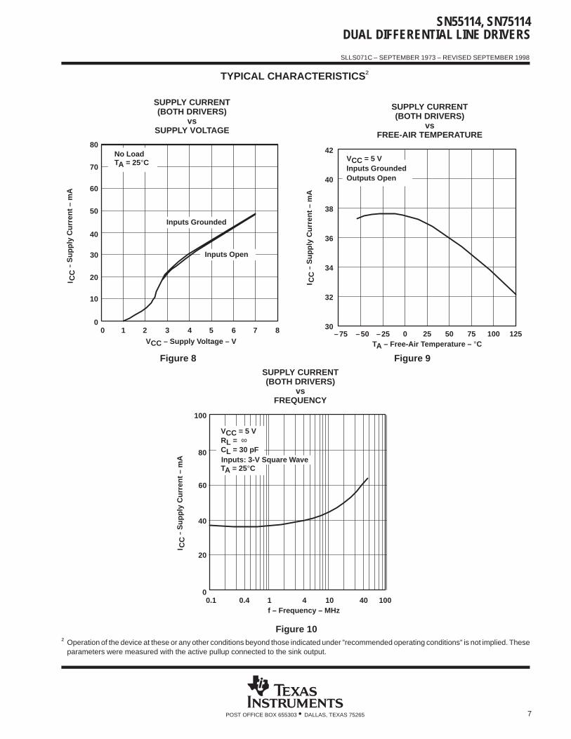
TYPICAL CHARACTERISTICS †
Figure 2
3
2
1
00 1 2
4
5
6
3 4
OUTPUT VOLTAGEvs
DATA INPUT VOLTAGE
VO
– O
utpu
t Vol
tage
– V
VI – Data Input Voltage – V
ÎÎÎÎÎÎÎÎ
VCC = 5.5 V
ÎÎÎÎÎÎÎÎ
VCC = 5 VÎÎÎÎÎÎÎÎ
VCC = 4.5 V
ÁÁÁÁV
O
ÁÁÁÁÁÁÁÁÁÁÁÁ
ÎÎÎÎÎÎÎÎ
No Load
ÎÎÎÎTA = 25°C
Figure 3
3
2
1
00 1 2
4
5
6
3 4
OUTPUT VOLTAGEvs
DATA INPUT VOLTAGE
VO
– O
utpu
t Vol
tage
– V
ÁÁÁÁ
V O
VI – Data Input Voltage – V
ÁÁÁÁÁÁÁÁÁÁÁÁ
ÎÎÎÎÎÎÎÎÎÎ
VCC = 5 VÎÎÎÎÎÎÎÎ
No Load
ÎÎÎÎÎTA = 125°C
ÎÎÎÎÎÎÎÎ
TA = 25°CÎÎÎÎÎÎÎÎÎÎ
TA = –55°C
† Operation of the device at these or any other conditions beyond those indicated under ”recommended operating conditions” is not implied. Theseparameters were measured with the active pullup connected to the sink output.

SN55114, SN75114DUAL DIFFERENTIAL LINE DRIVERS
SLLS071C – SEPTEMBER 1973 – REVISED SEPTEMBER 1998
6 POST OFFICE BOX 655303 • DALLAS, TEXAS 75265
TYPICAL CHARACTERISTICS †
Figure 4
3
2
1
0
4
5
HIGH-LEVEL OUTPUT VOLTAGEvs
HIGH-LEVEL OUTPUT CURRENT
– H
igh-
Leve
l Out
put V
olta
ge –
V
IOH – High-Level Output Current – mA
ÎÎÎÎVCC = 4.5 V
ÎÎÎÎÎÎÎÎÎÎ
TA = 25°C
ÁÁ
0 –20 –40 –60 –80 –100 –120
ÎÎÎÎÎÎÎÎ
VCC = 5.5 V
ÎÎÎÎÎVCC = 5 V
ÁÁÁÁÁÁÁÁÁ
V OH
Figure 5
LOW-LEVEL OUTPUT VOLTAGEvs
LOW-LEVEL OUTPUT CURRENT
– Lo
w-L
evel
Out
put V
olta
ge –
V
IOL – Low-Level Output Current – mA
0
0.4
800
10 20 30 40 50 60 70
0.1
0.2
0.3ÎÎÎÎÎÎÎÎÎÎ
VCC = 5.5 V
ÎÎÎÎÎÎÎÎÎÎ
VCC = 4.5 V
ÁÁÁÁÁÁ
VO
L
ÎÎÎÎÎÎÎÎÎÎ
TA = 25°C
Figure 6
1.2
0.8
0.4
00 25 50
1.6
2
2.4
75 100 125
OUTPUT VOLTAGEvs
FREE-AIR TEMPERATURE
VO
– O
utpu
t Vol
tage
– V
TA – Free-Air Temperature – °C
ÎÎÎÎÎÎÎÎÎÎ
VCC = 4.5 V
ÎÎÎÎÎÎÎÎÎÎÎÎ
VOH(IOH = –10 mA)3.2
2.8
3.6
4
–75 –50 –25
ÁÁÁÁÁÁ
VO
ÎÎÎÎÎÎÎVOH(IOH = –40 mA)
ÎÎÎÎÎÎÎÎÎÎVOL(IOL = 40 mA)
Figure 7
Pro
paga
tion
Del
ay T
imes
– n
s
40
0
10
20
30
1007550250 125
TA – Free-Air Temperature – °C
ÎÎÎÎÎÎ
tPLH
ÎÎÎtPHL
PROPAGATION DELAY TIMESvs
FREE-AIR TEMPERATURE
–75 –50 –25
ÁÁÁÁÁÁÁÁÁÁ
VCC = 5 VSee Figure 1
† Operation of the device at these or any other conditions beyond those indicated under ”recommended operating conditions” is not implied. Theseparameters were measured with the active pullup connected to the sink output.
SN55114, SN75114DUAL DIFFERENTIAL LINE DRIVERS
SLLS071C – SEPTEMBER 1973 – REVISED SEPTEMBER 1998
7POST OFFICE BOX 655303 • DALLAS, TEXAS 75265
TYPICAL CHARACTERISTICS †
Figure 8
40
20
10
00 1 2 3 4 5
60
70
80
6 7 8
50
30
SUPPLY CURRENT(BOTH DRIVERS)
vsSUPPLY VOLTAGE
ÎÎÎÎÎÎInputs Grounded
ÎÎÎÎÎÎÎÎÎÎ
Inputs Open
ICC
– S
uppl
y C
urre
nt –
mA
VCC – Supply Voltage – V
ÁÁÁÁÁÁ
CC
I
ÁÁÁÁÁÁÁÁÁÁÁÁ
ÎÎÎÎÎÎÎÎ
No Load
ÎÎÎÎTA = 25°C
Figure 9
–75 –50 –25
ICC
– S
uppl
y C
urre
nt –
mA
TA – Free-Air Temperature – °C
42
12530
0 25 50 75 100
32
34
36
38
40
SUPPLY CURRENT(BOTH DRIVERS)
vsFREE-AIR TEMPERATURE
ÁÁÁÁÁÁÁÁÁ
CC
I
ÁÁÁÁÁÁÁÁÁÁÁÁÁÁÁÁÁÁÁÁÁÁÁÁ
VCC = 5 VInputs GroundedOutputs Open
80
40
20
00.1 0.4 1 4 10 40 100
100
60
SUPPLY CURRENT(BOTH DRIVERS)
vsFREQUENCY
ICC
– S
uppl
y C
urre
nt –
mA
f – Frequency – MHz
ÁÁÁÁÁÁ
CC
I
ÁÁÁÁÁÁÁÁÁÁÁÁÁÁÁÁÁÁÁÁ
VCC = 5 VRL = ∞CL = 30 pF
TA = 25°C
ÁÁÁÁÁÁÁÁÁÁÁÁÁÁ
Inputs: 3-V Square Wave
Figure 10† Operation of the device at these or any other conditions beyond those indicated under ”recommended operating conditions” is not implied. These
parameters were measured with the active pullup connected to the sink output.

SN55114, SN75114DUAL DIFFERENTIAL LINE DRIVERS
SLLS071C – SEPTEMBER 1973 – REVISED SEPTEMBER 1998
8 POST OFFICE BOX 655303 • DALLAS, TEXAS 75265
APPLICATION INFORMATION
Twisted Pair
RT† RT†
1/2 SN75114Driver
1/2 SN75115Receiver
† RT = ZO. A capacitor can be connected in series with RT to reduce power dissipation.
Figure 11. Basic Party-Line or Data-Bus Differential Data Transmission

PACKAGE OPTION ADDENDUM
www.ti.com 22-Jan-2022
Addendum-Page 1
PACKAGING INFORMATION
Orderable Device Status(1)
Package Type PackageDrawing
Pins PackageQty
Eco Plan(2)
Lead finish/Ball material
(6)
MSL Peak Temp(3)
Op Temp (°C) Device Marking(4/5)
Samples
5962-88744022A ACTIVE LCCC FK 20 1 Non-RoHS& Green
SNPB N / A for Pkg Type -55 to 125 5962-88744022ASNJ55114FK
5962-8874402EA ACTIVE CDIP J 16 1 Non-RoHS& Green
SNPB N / A for Pkg Type -55 to 125 5962-8874402EASNJ55114J
5962-8874402FA ACTIVE CFP W 16 1 Non-RoHS& Green
SNPB N / A for Pkg Type -55 to 125 5962-8874402FASNJ55114W
JM38510/10403BEA ACTIVE CDIP J 16 1 Non-RoHS& Green
SNPB N / A for Pkg Type -55 to 125 JM38510/10403BEA
M38510/10403BEA ACTIVE CDIP J 16 1 Non-RoHS& Green
SNPB N / A for Pkg Type -55 to 125 JM38510/10403BEA
SN55114J ACTIVE CDIP J 16 1 Non-RoHS& Green
SNPB N / A for Pkg Type -55 to 125 SN55114J
SN75114D ACTIVE SOIC D 16 40 RoHS & Green NIPDAU Level-1-260C-UNLIM 0 to 70 SN751149614CD
SN75114DE4 ACTIVE SOIC D 16 40 RoHS & Green NIPDAU Level-1-260C-UNLIM 0 to 70 SN751149614CD
SN75114DG4 ACTIVE SOIC D 16 40 RoHS & Green NIPDAU Level-1-260C-UNLIM 0 to 70 SN751149614CD
SN75114N ACTIVE PDIP N 16 25 RoHS & Green NIPDAU N / A for Pkg Type 0 to 70 SN75114N
SNJ55114FK ACTIVE LCCC FK 20 1 Non-RoHS& Green
SNPB N / A for Pkg Type -55 to 125 5962-88744022ASNJ55114FK
SNJ55114J ACTIVE CDIP J 16 1 Non-RoHS& Green
SNPB N / A for Pkg Type -55 to 125 5962-8874402EASNJ55114J
SNJ55114W ACTIVE CFP W 16 1 Non-RoHS& Green
SNPB N / A for Pkg Type -55 to 125 5962-8874402FASNJ55114W
(1) The marketing status values are defined as follows:ACTIVE: Product device recommended for new designs.LIFEBUY: TI has announced that the device will be discontinued, and a lifetime-buy period is in effect.NRND: Not recommended for new designs. Device is in production to support existing customers, but TI does not recommend using this part in a new design.

PACKAGE OPTION ADDENDUM
www.ti.com 22-Jan-2022
Addendum-Page 2
PREVIEW: Device has been announced but is not in production. Samples may or may not be available.OBSOLETE: TI has discontinued the production of the device.
(2) RoHS: TI defines "RoHS" to mean semiconductor products that are compliant with the current EU RoHS requirements for all 10 RoHS substances, including the requirement that RoHS substancedo not exceed 0.1% by weight in homogeneous materials. Where designed to be soldered at high temperatures, "RoHS" products are suitable for use in specified lead-free processes. TI mayreference these types of products as "Pb-Free".RoHS Exempt: TI defines "RoHS Exempt" to mean products that contain lead but are compliant with EU RoHS pursuant to a specific EU RoHS exemption.Green: TI defines "Green" to mean the content of Chlorine (Cl) and Bromine (Br) based flame retardants meet JS709B low halogen requirements of <=1000ppm threshold. Antimony trioxide basedflame retardants must also meet the <=1000ppm threshold requirement.
(3) MSL, Peak Temp. - The Moisture Sensitivity Level rating according to the JEDEC industry standard classifications, and peak solder temperature.
(4) There may be additional marking, which relates to the logo, the lot trace code information, or the environmental category on the device.
(5) Multiple Device Markings will be inside parentheses. Only one Device Marking contained in parentheses and separated by a "~" will appear on a device. If a line is indented then it is a continuationof the previous line and the two combined represent the entire Device Marking for that device.
(6) Lead finish/Ball material - Orderable Devices may have multiple material finish options. Finish options are separated by a vertical ruled line. Lead finish/Ball material values may wrap to twolines if the finish value exceeds the maximum column width.
Important Information and Disclaimer:The information provided on this page represents TI's knowledge and belief as of the date that it is provided. TI bases its knowledge and belief on informationprovided by third parties, and makes no representation or warranty as to the accuracy of such information. Efforts are underway to better integrate information from third parties. TI has taken andcontinues to take reasonable steps to provide representative and accurate information but may not have conducted destructive testing or chemical analysis on incoming materials and chemicals.TI and TI suppliers consider certain information to be proprietary, and thus CAS numbers and other limited information may not be available for release.
In no event shall TI's liability arising out of such information exceed the total purchase price of the TI part(s) at issue in this document sold by TI to Customer on an annual basis.
OTHER QUALIFIED VERSIONS OF SN55114, SN75114 :
• Catalog : SN75114
• Military : SN55114
NOTE: Qualified Version Definitions:
• Catalog - TI's standard catalog product
• Military - QML certified for Military and Defense Applications

TUBE
*All dimensions are nominal
Device Package Name Package Type Pins SPQ L (mm) W (mm) T (µm) B (mm)
5962-88744022A FK LCCC 20 1 506.98 12.06 2030 NA
SN75114D D SOIC 16 40 507 8 3940 4.32
SN75114DE4 D SOIC 16 40 507 8 3940 4.32
SN75114DG4 D SOIC 16 40 507 8 3940 4.32
SN75114N N PDIP 16 25 506 13.97 11230 4.32
SNJ55114FK FK LCCC 20 1 506.98 12.06 2030 NA
PACKAGE MATERIALS INFORMATION
www.ti.com 5-Jan-2022
Pack Materials-Page 1


IMPORTANT NOTICE AND DISCLAIMERTI PROVIDES TECHNICAL AND RELIABILITY DATA (INCLUDING DATA SHEETS), DESIGN RESOURCES (INCLUDING REFERENCE DESIGNS), APPLICATION OR OTHER DESIGN ADVICE, WEB TOOLS, SAFETY INFORMATION, AND OTHER RESOURCES “AS IS” AND WITH ALL FAULTS, AND DISCLAIMS ALL WARRANTIES, EXPRESS AND IMPLIED, INCLUDING WITHOUT LIMITATION ANY IMPLIED WARRANTIES OF MERCHANTABILITY, FITNESS FOR A PARTICULAR PURPOSE OR NON-INFRINGEMENT OF THIRD PARTY INTELLECTUAL PROPERTY RIGHTS.These resources are intended for skilled developers designing with TI products. You are solely responsible for (1) selecting the appropriate TI products for your application, (2) designing, validating and testing your application, and (3) ensuring your application meets applicable standards, and any other safety, security, regulatory or other requirements.These resources are subject to change without notice. TI grants you permission to use these resources only for development of an application that uses the TI products described in the resource. Other reproduction and display of these resources is prohibited. No license is granted to any other TI intellectual property right or to any third party intellectual property right. TI disclaims responsibility for, and you will fully indemnify TI and its representatives against, any claims, damages, costs, losses, and liabilities arising out of your use of these resources.TI’s products are provided subject to TI’s Terms of Sale or other applicable terms available either on ti.com or provided in conjunction with such TI products. TI’s provision of these resources does not expand or otherwise alter TI’s applicable warranties or warranty disclaimers for TI products.TI objects to and rejects any additional or different terms you may have proposed. IMPORTANT NOTICE
Mailing Address: Texas Instruments, Post Office Box 655303, Dallas, Texas 75265Copyright © 2022, Texas Instruments Incorporated