Embed Size (px)
Citation preview
Product
Folder
Sample &Buy
Technical
Documents
Tools &
Software
Support &Community
SN65LVDS93ASLLS992B –AUGUST 2009–REVISED MARCH 2015
SN65LVDS93A FlatLink™ Transmitter1 Features 2 Applications1• Industrial Temperature Range –40°C to 85°C • LCD Display Panel Drivers• LVDS Display Serdes Interfaces Directly to LCD • UMPC and Netbook PCs
Display Panels With Integrated LVDS • Digital Picture Frames• Package Options: 4.5-mm × 7-mm BGA, and 8.1-
3 Descriptionmm × 14-mm TSSOPThe SN65LVDS93A LVDS SerDes• 1.8 V up to 3.3-V Tolerant Data Inputs to Connect(serializer/deserializer) transmitter contains four 7-bitDirectly to Low-Power, Low-Voltage Applicationparallel load serial-out shift registers, a 7 × clockand Graphic Processorssynthesizer, and five low-voltage differential signaling• Transfer Rate up to 135 Mpps (Mega Pixels Per (LVDS) drivers in a single integrated circuit. These
Second); Pixel Clock Frequency Range 10 MHz to functions allow synchronous transmission of 28 bits of135 MHz single-ended LVTTL data over five balanced-pair
conductors for receipt by a compatible receiver, such• Suited for Display Resolutions Ranging Fromas the SN65LVDS94 (SLLS928).HVGA up to HD With Low EMI
• Operates From a Single 3.3-V Supply and 170 When transmitting, data bits D0 through D27 aremW (Typical) at 75 MHz each loaded into registers upon the edge of the input
clock signal (CLKIN). The rising or falling edge of the• 28 Data Channels Plus Clock In Low-Voltage TTLclock can be selected through the clock selectto 4 Data Channels Plus Clock Out Low-Voltage(CLKSEL) pin. The frequency of CLKIN is multipliedDifferential seven times and then used to serially unload the data
• Consumes Less Than 1 mW When Disabled registers in 7-bit slices. The four serial streams and aphase-locked clock (CLKOUT) are then output to• Selectable Rising or Falling Clock Edge TriggeredLVDS output drivers. The frequency of CLKOUT isInputsthe same as the input clock, CLKIN.• ESD: 5-kV HBM
• Supports Spread Spectrum Clocking (SSC) Device Information(1)
• Compatible With all OMAP™2x, OMAP3x, and PART NUMBER PACKAGE BODY SIZE (NOM)DaVinci™ Application Processors TSSOP (56) 14.00 mm × 6.10 mm
SN65LVDS93A BGA MICROSTAR 7.00 mm × 4.50 mmJUNIOR (56)
(1) For all available packages, see the orderable addendum atthe end of the data sheet.
RGB Video System Using Discrete LVDS TX
1
An IMPORTANT NOTICE at the end of this data sheet addresses availability, warranty, changes, use in safety-critical applications,intellectual property matters and other important disclaimers. PRODUCTION DATA.
SN65LVDS93ASLLS992B –AUGUST 2009–REVISED MARCH 2015 www.ti.com
Table of Contents9.1 Overview ................................................................. 161 Features .................................................................. 19.2 Functional Block Diagram ....................................... 162 Applications ........................................................... 19.3 Feature Description................................................. 173 Description ............................................................. 19.4 Device Functional Modes........................................ 184 Revision History..................................................... 2
10 Application and Implementation........................ 195 Description (continued)......................................... 310.1 Application Information.......................................... 196 Pin Configuration and Functions ......................... 310.2 Typical Application ................................................ 207 Specifications......................................................... 6 11 Power Supply Recommendations ..................... 277.1 Absolute Maximum Ratings ..................................... 6
12 Layout................................................................... 277.2 ESD Ratings.............................................................. 612.1 Layout Guidelines ................................................. 277.3 Recommended Operating Conditions....................... 712.2 Layout Example .................................................... 297.4 Thermal Information .................................................. 7
13 Device and Documentation Support ................. 317.5 Electrical Characteristics........................................... 713.1 Documentation Support ........................................ 317.6 Timing Requirements ................................................ 813.2 Trademarks ........................................................... 317.7 Switching Characteristics .......................................... 913.3 Electrostatic Discharge Caution............................ 317.8 Typical Characteristics ............................................ 1113.4 Glossary ................................................................ 318 Parameter Measurement Information ................ 12
14 Mechanical, Packaging, and Orderable9 Detailed Description ............................................ 16 Information ........................................................... 31
4 Revision HistoryNOTE: Page numbers for previous revisions may differ from page numbers in the current version.
Changes from Revision A (August 2011) to Revision B Page
• Added Pin Configuration and Functions section, ESD Ratings table, Feature Description section, Device FunctionalModes, Application and Implementation section, Power Supply Recommendations section, Layout section, Deviceand Documentation Support section, and Mechanical, Packaging, and Orderable Information section .............................. 1
Changes from Original (August 2009) to Revision A Page
• Deleted all maximum values from ICC - Supply current (average).......................................................................................... 8• Changed ten - Enable Time, unit value From: 6 ns To: 6 µs................................................................................................... 9
2 Submit Documentation Feedback Copyright © 2009–2015, Texas Instruments Incorporated
Product Folder Links: SN65LVDS93A
1
2
3
4
5
6
7
8
9
10
11
12
13
14
15
16
17
18
19
20
21
22
23
24
25
26
27
28 29
30
31
32
33
34
35
36
37
38
39
40
41
42
43
44
45
46
47
48
49
50
51
52
53
54
55
56IOVCC
VCC
LVDSVCCGND
CLKSEL
D16
D15
D14 GND
CLKOUTM
D13
D17
D5
D6
D7
D8
D10
D11
D18
GND
D21
D23
D24
D2
D3
D4
GND
D1
D0
D27
GND
Y0M
GND
GND
PLLVCC
GND
SHTDN
CLKIN
D26
GND
GND
D9
D12
D19
D20
D22
IOVCC
D25
Y0P
Y1M
Y1P
Y2M
Y2P
Y3M
Y3P
CLKOUTP
13 2456
K
G
H
J
D
E
F
C
D13
D14
D16
D17
GND Y3M
D15
GND
GND
GND
Y1P
Y2P
LVDSVCC
Y1M
Y2M
GND
Y0M
CLKMCLKSEL
D8
CLKP
Y0P
D12
D11
D19
D3
D1
D27D6
D7
GND
D4D5
D0
D2
Y3P
D18
B
A
D22
D20
D26
GND
GNDD24
D21
D23
SHTDND25
CLKIN
PLLVCC
IOVCC
IOVCC
VCC
GND
GND
D10
D9
SN65LVDS93Awww.ti.com SLLS992B –AUGUST 2009–REVISED MARCH 2015
5 Description (continued)The SN65LVDS93A device requires no external components and little or no control. The data bus appears thesame at the input to the transmitter and output of the receiver with the data transmission transparent to theusers. The only user intervention is selecting a clock rising edge by inputting a high level to CLKSEL or a fallingedge with a low-level input and the possible use of the shutdown/clear (SHTDN) signal. SHTDN is an active-lowinput to inhibit the clock and shut off the LVDS output drivers for lower power consumption. A low level on thissignal clears all internal registers at a low level.
The SN65LVDS93A is characterized for operation over ambient air temperatures of –40°C to 85°C.
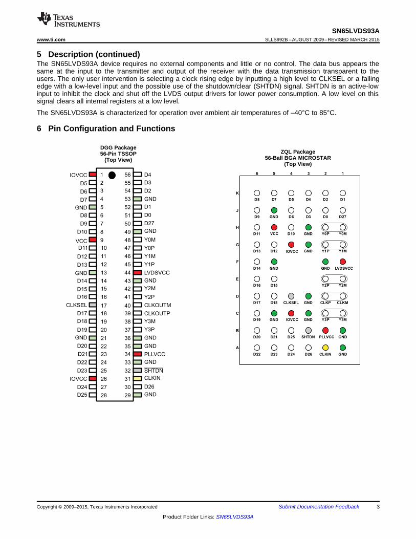
6 Pin Configuration and Functions
DGG PackageZQL Package56-Pin TSSOP
56-Ball BGA MICROSTAR(Top View)(Top View)
Copyright © 2009–2015, Texas Instruments Incorporated Submit Documentation Feedback 3
Product Folder Links: SN65LVDS93A
SN65LVDS93ASLLS992B –AUGUST 2009–REVISED MARCH 2015 www.ti.com
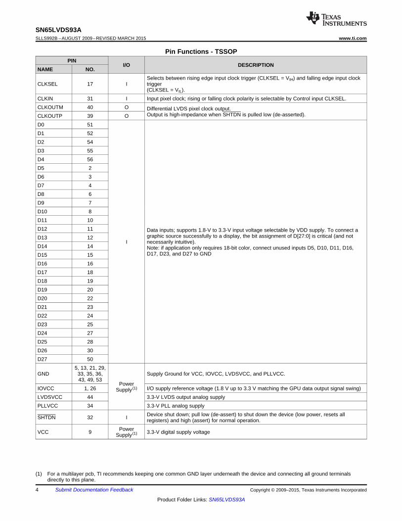
Pin Functions - TSSOPPIN
I/O DESCRIPTIONNAME NO.
Selects between rising edge input clock trigger (CLKSEL = VIH) and falling edge input clockCLKSEL 17 I trigger
(CLKSEL = VIL).CLKIN 31 I Input pixel clock; rising or falling clock polarity is selectable by Control input CLKSEL.CLKOUTM 40 O Differential LVDS pixel clock output.
Output is high-impedance when SHTDN is pulled low (de-asserted).CLKOUTP 39 OD0 51D1 52D2 54D3 55D4 56D5 2D6 3D7 4D8 6D9 7D10 8D11 10D12 11 Data inputs; supports 1.8-V to 3.3-V input voltage selectable by VDD supply. To connect a
graphic source successfully to a display, the bit assignment of D[27:0] is critical (and notD13 12I necessarily intuitive).
D14 14 Note: if application only requires 18-bit color, connect unused inputs D5, D10, D11, D16,D17, D23, and D27 to GNDD15 15
D16 16D17 18D18 19D19 20D20 22D21 23D22 24D23 25D24 27D25 28D26 30D27 50
5, 13, 21, 29,GND 33, 35, 36, Supply Ground for VCC, IOVCC, LVDSVCC, and PLLVCC.
43, 49, 53Power
IOVCC 1, 26 I/O supply reference voltage (1.8 V up to 3.3 V matching the GPU data output signal swing)Supply (1)
LVDSVCC 44 3.3-V LVDS output analog supplyPLLVCC 34 3.3-V PLL analog supply
Device shut down; pull low (de-assert) to shut down the device (low power, resets allSHTDN 32 I registers) and high (assert) for normal operation.PowerVCC 9 3.3-V digital supply voltageSupply (1)
(1) For a multilayer pcb, TI recommends keeping one common GND layer underneath the device and connecting all ground terminalsdirectly to this plane.
4 Submit Documentation Feedback Copyright © 2009–2015, Texas Instruments Incorporated
Product Folder Links: SN65LVDS93A
SN65LVDS93Awww.ti.com SLLS992B –AUGUST 2009–REVISED MARCH 2015
Pin Functions - TSSOP (continued)PIN
I/O DESCRIPTIONNAME NO.Y0M 48Y1M 46Y2M 42 Differential LVDS data outputs.O Outputs are high-impedance when SHTDN is pulled low (de-asserted)Y0P 47Y1P 45Y2P 41Y3M 38 Differential LVDS Data outputs.
O Output is high-impedance when SHTDN is pulled low (de-asserted).Y3P 37 Note: if the application only requires 18-bit color, this output can be left open.
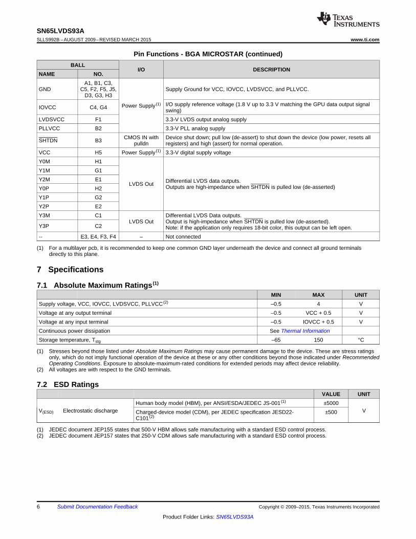
Pin Functions - BGA MICROSTARBALL
I/O DESCRIPTIONNAME NO.
CMOS IN withCLKIN A2 Input pixel clock; rising or falling clock polarity is selectable by Control input CLKSEL.pulldnCLKM D1 Differential LVDS pixel clock output.LVDS Out Output is high-impedance when SHTDN is pulled low (de-asserted).CLKP D2
Selects between rising edge input clock trigger (CLKSEL = VIH) and falling edge inputCMOS IN withCLKSEL D4 clock triggerpulldn (CLKSEL = VIL).D0 J2D1 K1D2 K2D3 J3D4 K3D5 K4D6 J4D7 K5D8 K6D9 J6D10 H4D11 H6D12 G5 Data inputs; supports 1.8-V to 3.3-V input voltage selectable by VDD supply. To
connect a graphic source successfully to a display, the bit assignment of D[27:0] isD13 G6 CMOS IN with critical (and not necessarily intuitive).pulldnD14 F6 Note: if application only requires 18-bit color, connect unused inputs D5, D10, D11,D16, D17, D23, and D27 to GND.D15 E5
D16 E6D17 D6D18 D5D19 C6D20 B6D21 B5D22 A6D23 A5D24 A4D25 B4D26 A3D27 J1
Copyright © 2009–2015, Texas Instruments Incorporated Submit Documentation Feedback 5
Product Folder Links: SN65LVDS93A
SN65LVDS93ASLLS992B –AUGUST 2009–REVISED MARCH 2015 www.ti.com
Pin Functions - BGA MICROSTAR (continued)BALL
I/O DESCRIPTIONNAME NO.
A1, B1, C3,GND C5, F2, F5, J5, Supply Ground for VCC, IOVCC, LVDSVCC, and PLLVCC.
D3, G3, H3I/O supply reference voltage (1.8 V up to 3.3 V matching the GPU data output signalPower Supply (1)
IOVCC C4, G4 swing)LVDSVCC F1 3.3-V LVDS output analog supplyPLLVCC B2 3.3-V PLL analog supply
CMOS IN with Device shut down; pull low (de-assert) to shut down the device (low power, resets allSHTDN B3 pulldn registers) and high (assert) for normal operation.VCC H5 Power Supply (1) 3.3-V digital supply voltageY0M H1Y1M G1Y2M E1 Differential LVDS data outputs.LVDS Out Outputs are high-impedance when SHTDN is pulled low (de-asserted)Y0P H2Y1P G2Y2P E2Y3M C1 Differential LVDS Data outputs.
LVDS Out Output is high-impedance when SHTDN is pulled low (de-asserted).Y3P C2 Note: if the application only requires 18-bit color, this output can be left open.-- E3, E4, F3, F4 – Not connected
(1) For a multilayer pcb, it is recommended to keep one common GND layer underneath the device and connect all ground terminalsdirectly to this plane.
7 Specifications
7.1 Absolute Maximum Ratings (1)
MIN MAX UNITSupply voltage, VCC, IOVCC, LVDSVCC, PLLVCC (2) –0.5 4 VVoltage at any output terminal –0.5 VCC + 0.5 VVoltage at any input terminal –0.5 IOVCC + 0.5 VContinuous power dissipation See Thermal InformationStorage temperature, Tstg –65 150 °C
(1) Stresses beyond those listed under Absolute Maximum Ratings may cause permanent damage to the device. These are stress ratingsonly, which do not imply functional operation of the device at these or any other conditions beyond those indicated under RecommendedOperating Conditions. Exposure to absolute-maximum-rated conditions for extended periods may affect device reliability.
(2) All voltages are with respect to the GND terminals.
7.2 ESD RatingsVALUE UNIT
Human body model (HBM), per ANSI/ESDA/JEDEC JS-001 (1) ±5000V(ESD) Electrostatic discharge VCharged-device model (CDM), per JEDEC specification JESD22- ±500
C101 (2)
(1) JEDEC document JEP155 states that 500-V HBM allows safe manufacturing with a standard ESD control process.(2) JEDEC document JEP157 states that 250-V CDM allows safe manufacturing with a standard ESD control process.
6 Submit Documentation Feedback Copyright © 2009–2015, Texas Instruments Incorporated
Product Folder Links: SN65LVDS93A
SN65LVDS93Awww.ti.com SLLS992B –AUGUST 2009–REVISED MARCH 2015
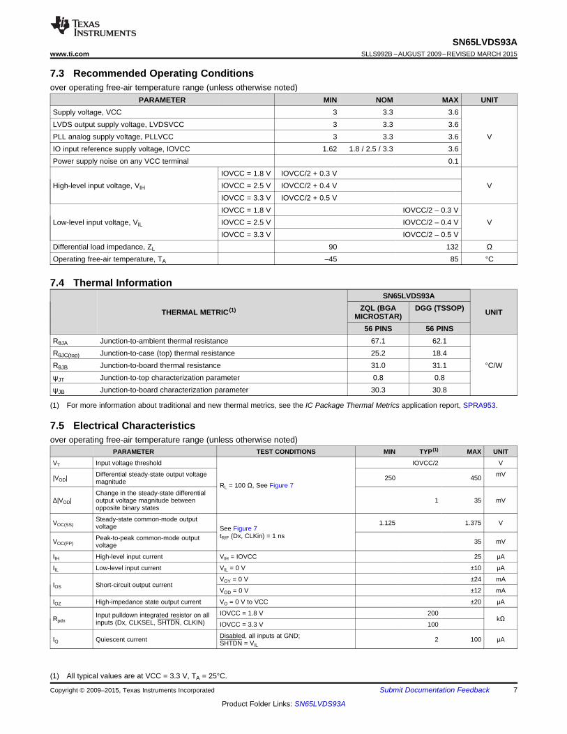
7.3 Recommended Operating Conditionsover operating free-air temperature range (unless otherwise noted)
PARAMETER MIN NOM MAX UNITSupply voltage, VCC 3 3.3 3.6LVDS output supply voltage, LVDSVCC 3 3.3 3.6PLL analog supply voltage, PLLVCC 3 3.3 3.6 VIO input reference supply voltage, IOVCC 1.62 1.8 / 2.5 / 3.3 3.6Power supply noise on any VCC terminal 0.1
IOVCC = 1.8 V IOVCC/2 + 0.3 VHigh-level input voltage, VIH IOVCC = 2.5 V IOVCC/2 + 0.4 V V
IOVCC = 3.3 V IOVCC/2 + 0.5 VIOVCC = 1.8 V IOVCC/2 – 0.3 V
Low-level input voltage, VIL IOVCC = 2.5 V IOVCC/2 – 0.4 V VIOVCC = 3.3 V IOVCC/2 – 0.5 V
Differential load impedance, ZL 90 132 ΩOperating free-air temperature, TA –45 85 °C
7.4 Thermal InformationSN65LVDS93A
ZQL (BGA DGG (TSSOP)THERMAL METRIC (1) UNITMICROSTAR)56 PINS 56 PINS
RθJA Junction-to-ambient thermal resistance 67.1 62.1RθJC(top) Junction-to-case (top) thermal resistance 25.2 18.4RθJB Junction-to-board thermal resistance 31.0 31.1 °C/WψJT Junction-to-top characterization parameter 0.8 0.8ψJB Junction-to-board characterization parameter 30.3 30.8
(1) For more information about traditional and new thermal metrics, see the IC Package Thermal Metrics application report, SPRA953.
7.5 Electrical Characteristicsover operating free-air temperature range (unless otherwise noted)
PARAMETER TEST CONDITIONS MIN TYP (1) MAX UNIT
VT Input voltage threshold IOVCC/2 V
Differential steady-state output voltage mV|VOD| 250 450magnitude RL = 100 Ω, See Figure 7Change in the steady-state differential
Δ|VOD| output voltage magnitude between 1 35 mVopposite binary states
Steady-state common-mode outputVOC(SS) 1.125 1.375 Vvoltage See Figure 7tR/F (Dx, CLKin) = 1 nsPeak-to-peak common-mode outputVOC(PP) 35 mVvoltage
IIH High-level input current VIH = IOVCC 25 μA
IIL Low-level input current VIL = 0 V ±10 μA
VOY = 0 V ±24 mAIOS Short-circuit output current
VOD = 0 V ±12 mA
IOZ High-impedance state output current VO = 0 V to VCC ±20 μA
IOVCC = 1.8 V 200Input pulldown integrated resistor on allRpdn kΩinputs (Dx, CLKSEL, SHTDN, CLKIN) IOVCC = 3.3 V 100
Disabled, all inputs at GND;IQ Quiescent current 2 100 μASHTDN = VIL
(1) All typical values are at VCC = 3.3 V, TA = 25°C.
Copyright © 2009–2015, Texas Instruments Incorporated Submit Documentation Feedback 7
Product Folder Links: SN65LVDS93A
SN65LVDS93ASLLS992B –AUGUST 2009–REVISED MARCH 2015 www.ti.com
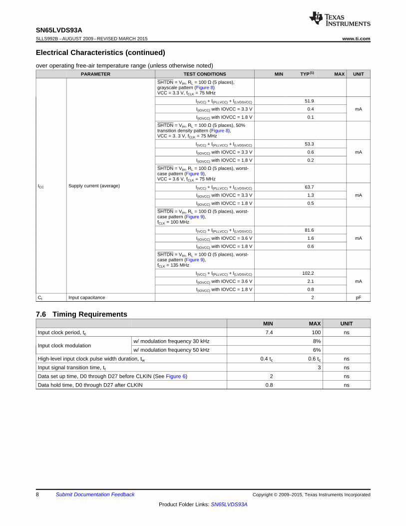
Electrical Characteristics (continued)over operating free-air temperature range (unless otherwise noted)
PARAMETER TEST CONDITIONS MIN TYP (1) MAX UNIT
SHTDN = VIH, RL = 100 Ω (5 places),grayscale pattern (Figure 8)VCC = 3.3 V, fCLK = 75 MHz
I(VCC) + I(PLLVCC) + I(LVDSVCC) 51.9
I(IOVCC) with IOVCC = 3.3 V 0.4 mA
I(IOVCC) with IOVCC = 1.8 V 0.1
SHTDN = VIH, RL = 100 Ω (5 places), 50%transition density pattern (Figure 8),VCC = 3. 3 V, fCLK = 75 MHz
I(VCC) + I(PLLVCC) + I(LVDSVCC) 53.3
I(IOVCC) with IOVCC = 3.3 V 0.6 mA
I(IOVCC) with IOVCC = 1.8 V 0.2
SHTDN = VIH, RL = 100 Ω (5 places), worst-case pattern (Figure 9),VCC = 3.6 V, fCLK = 75 MHz
ICC Supply current (average) I(VCC) + I(PLLVCC) + I(LVDSVCC) 63.7
I(IOVCC) with IOVCC = 3.3 V 1.3 mA
I(IOVCC) with IOVCC = 1.8 V 0.5
SHTDN = VIH, RL = 100 Ω (5 places), worst-case pattern (Figure 9),fCLK = 100 MHz
I(VCC) + I(PLLVCC) + I(LVDSVCC) 81.6
I(IOVCC) with IOVCC = 3.6 V 1.6 mA
I(IOVCC) with IOVCC = 1.8 V 0.6
SHTDN = VIH, RL = 100 Ω (5 places), worst-case pattern (Figure 9),fCLK = 135 MHz
I(VCC) + I(PLLVCC) + I(LVDSVCC) 102.2
I(IOVCC) with IOVCC = 3.6 V 2.1 mA
I(IOVCC) with IOVCC = 1.8 V 0.8
CI Input capacitance 2 pF
7.6 Timing RequirementsMIN MAX UNIT
Input clock period, tc 7.4 100 nsw/ modulation frequency 30 kHz 8%
Input clock modulationw/ modulation frequency 50 kHz 6%
High-level input clock pulse width duration, tw 0.4 tc 0.6 tc nsInput signal transition time, tt 3 nsData set up time, D0 through D27 before CLKIN (See Figure 6) 2 nsData hold time, D0 through D27 after CLKIN 0.8 ns
8 Submit Documentation Feedback Copyright © 2009–2015, Texas Instruments Incorporated
Product Folder Links: SN65LVDS93A
SN65LVDS93Awww.ti.com SLLS992B –AUGUST 2009–REVISED MARCH 2015
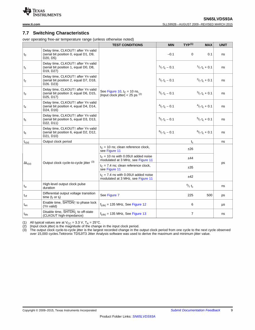
7.7 Switching Characteristicsover operating free-air temperature range (unless otherwise noted)
TEST CONDITIONS MIN TYP (1) MAX UNITDelay time, CLKOUT↑ after Yn valid
t0 (serial bit position 0, equal D1, D9, –0.1 0 0.1 nsD20, D5)Delay time, CLKOUT↑ after Yn valid
t1 (serial bit position 1, equal D0, D8, 1/7 tc – 0.1 1/7 tc + 0.1 nsD19, D27)Delay time, CLKOUT↑ after Yn valid
t2 (serial bit position 2, equal D7, D18, 2/7 tc – 0.1 2/7 tc + 0.1 nsD26. D23)Delay time, CLKOUT↑ after Yn valid See Figure 10, tC = 10 ns,t3 (serial bit position 3; equal D6, D15, 3/7 tc – 0.1 3/7 tc + 0.1 ns|Input clock jitter| < 25 ps (2)D25, D17)Delay time, CLKOUT↑ after Yn valid
t4 (serial bit position 4, equal D4, D14, 4/7 tc – 0.1 4/7 tc + 0.1 nsD24, D16)Delay time, CLKOUT↑ after Yn valid
t5 (serial bit position 5, equal D3, D13, 5/7 tc – 0.1 5/7 tc + 0.1 nsD22, D11)Delay time, CLKOUT↑ after Yn valid
t6 (serial bit position 6, equal D2, D12, 6/7 tc – 0.1 6/7 tc + 0.1 nsD21, D10)
tc(o) Output clock period tc nstC = 10 ns; clean reference clock, ±26see Figure 11tC = 10 ns with 0.05UI added noise ±44modulated at 3 MHz, see Figure 11
Δtc(o) Output clock cycle-to-cycle jitter (3) pstC = 7.4 ns; clean reference clock, ±35see Figure 11tC = 7.4 ns with 0.05UI added noise ±42modulated at 3 MHz, see Figure 11
High-level output clock pulsetw 4/7 tc nsdurationDifferential output voltage transitiontr/f See Figure 7 225 500 pstime (tr or tf)Enable time, SHTDN↑ to phase lockten f(clk) = 135 MHz, See Figure 12 6 µs(Yn valid)Disable time, SHTDN↓ to off-statetdis f(clk) = 135 MHz, See Figure 13 7 ns(CLKOUT high-impedance)
(1) All typical values are at VCC = 3.3 V, TA = 25°C.(2) |Input clock jitter| is the magnitude of the change in the input clock period.(3) The output clock cycle-to-cycle jitter is the largest recorded change in the output clock period from one cycle to the next cycle observed
over 15,000 cycles.Tektronix TDSJIT3 Jitter Analysis software was used to derive the maximum and minimum jitter value.
Copyright © 2009–2015, Texas Instruments Incorporated Submit Documentation Feedback 9
Product Folder Links: SN65LVDS93A
D0-1
D8-1
D19-1
D27-1
D7
D18
D26
D23 D17
D25
D15
D6
D16
D24
D14
D4
D11
D22
D13
D3
D10
D21
D12
D2
D5
D20
D9
D1
D27
D19
D8
D0
D23+1
D26+1
D18+1
D7+1
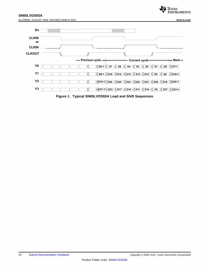
Dn
CLKIN
CLKOUT
Y0
Y1
Y2
Y3
Previous cycle Current cycle Next
CLKIN
or
SN65LVDS93ASLLS992B –AUGUST 2009–REVISED MARCH 2015 www.ti.com
Figure 1. Typical SN65LVDS93A Load and Shift Sequences
10 Submit Documentation Feedback Copyright © 2009–2015, Texas Instruments Incorporated
Product Folder Links: SN65LVDS93A
CLKL Signal PRBS Data Signal
t - Time - 1 ns/divk
V -
Vo
ltag
e -
80m
V/d
iv
f - Clock Frequency - MHzclk
50
10 30 50 70 90 110 130
I-
Av
era
ge
Su
pp
ly C
urr
en
t -
mA
CC
20
30
70
40
90
60
80
V = 3.6VCC
V = 3.3VCC
V = 3VCC
100
300
0.01 0.10 10
Pe
rio
d C
loc
k J
itte
r -
ps
-pp
f - Input Modular Frequency - MHz(mod)
0
100
500
200
600
400
800
700
1
Output Jitter
Input Jitter
SN65LVDS93Awww.ti.com SLLS992B –AUGUST 2009–REVISED MARCH 2015
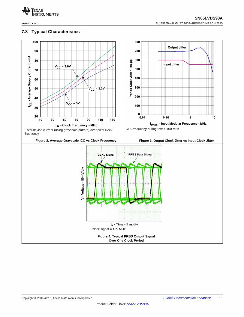
7.8 Typical Characteristics
CLK frequency during text = 100 MHzTotal device current (using grayscale pattern) over pixel clockfrequency
Figure 2. Average Grayscale ICC vs Clock Frequency Figure 3. Output Clock Jitter vs Input Clock Jitter
Clock signal = 135 MHz
Figure 4. Typical PRBS Output SignalOver One Clock Period
Copyright © 2009–2015, Texas Instruments Incorporated Submit Documentation Feedback 11
Product Folder Links: SN65LVDS93A
tsu thold
Dn
CLKIN
7V
D or
IOVCC
LVDSVCC
SHTDN50W
7V
5WYnP or
YnM10kW
300kW
SN65LVDS93ASLLS992B –AUGUST 2009–REVISED MARCH 2015 www.ti.com
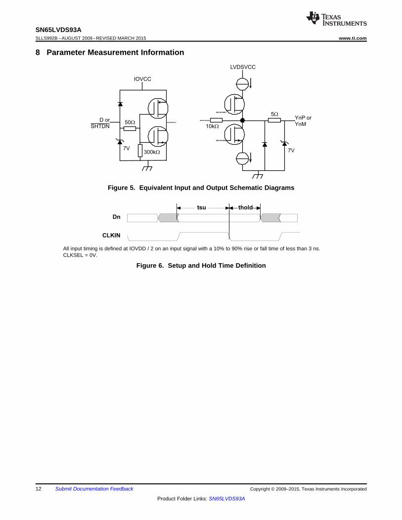
8 Parameter Measurement Information
Figure 5. Equivalent Input and Output Schematic Diagrams
All input timing is defined at IOVDD / 2 on an input signal with a 10% to 90% rise or fall time of less than 3 ns.CLKSEL = 0V.
Figure 6. Setup and Hold Time Definition
12 Submit Documentation Feedback Copyright © 2009–2015, Texas Instruments Incorporated
Product Folder Links: SN65LVDS93A
CLKIN
D0,8,16
D1,9,17
D2,10,18
D3,11,19
D4-7,12-15,20-23
D24-27
VOD
49.9 ± 1% (2 PLCS)WYP
YM
tf tr
0%
20%
80%
100%
0V
0V
VOC
VOD(H)
VOC(SS)
VOD(L)
VOC(SS)
VOC(PP)
SN65LVDS93Awww.ti.com SLLS992B –AUGUST 2009–REVISED MARCH 2015
Parameter Measurement Information (continued)
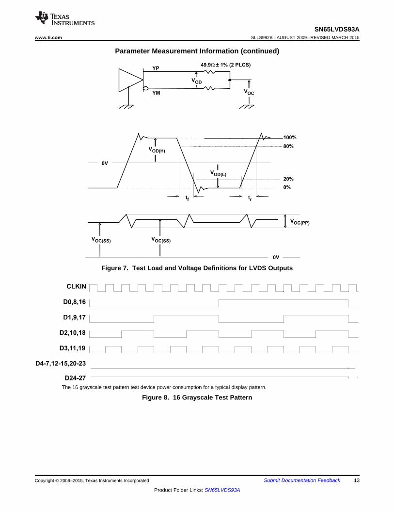
Figure 7. Test Load and Voltage Definitions for LVDS Outputs
The 16 grayscale test pattern test device power consumption for a typical display pattern.
Figure 8. 16 Grayscale Test Pattern
Copyright © 2009–2015, Texas Instruments Incorporated Submit Documentation Feedback 13
Product Folder Links: SN65LVDS93A
t7
t0
t1
t2
t3
t4
t5
t6
CLKIN
CLKOUT
Yn
VOD(L)
0.00V
t0-6t7
1.40V
~2.5V
~0.5V
CLKIN
CLKOUTor Yn
VOD(H)
T
CLKIN
EVEN Dn
ODD Dn
SN65LVDS93ASLLS992B –AUGUST 2009–REVISED MARCH 2015 www.ti.com
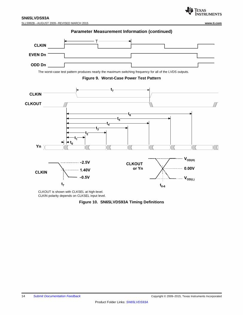
Parameter Measurement Information (continued)
The worst-case test pattern produces nearly the maximum switching frequency for all of the LVDS outputs.
Figure 9. Worst-Case Power Test Pattern
CLKOUT is shown with CLKSEL at high-level.CLKIN polarity depends on CLKSEL input level.
Figure 10. SN65LVDS93A Timing Definitions
14 Submit Documentation Feedback Copyright © 2009–2015, Texas Instruments Incorporated
Product Folder Links: SN65LVDS93A
tdis
CLKIN
SHTDN
CLKOUT
ten
Invalid
Valid
CLKIN
Dn
SHTDN
Yn
VCO
DeviceUnderTest
Reference
Modulation
v(t) = A sin(2 pf t)mod
+
+
HP8656B SignalGenerator,
0.1 MHz-990 MHz
RF Output
HP8665A SynthesizedSignal Generator,0.1 MHz-4200 MHz
RF Output
Modulation Input
Device UnderTest
CLKIN CLKOUT
DTS2070CDigital
TimeScope
Input
SN65LVDS93Awww.ti.com SLLS992B –AUGUST 2009–REVISED MARCH 2015
Parameter Measurement Information (continued)
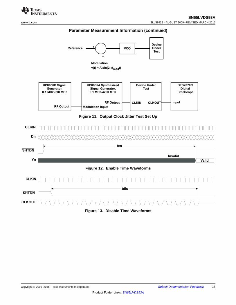
Figure 11. Output Clock Jitter Test Set Up
Figure 12. Enable Time Waveforms
Figure 13. Disable Time Waveforms
Copyright © 2009–2015, Texas Instruments Incorporated Submit Documentation Feedback 15
Product Folder Links: SN65LVDS93A
Parallel-Load 7-bitShift Register
A,B,...GSHIFT/LOAD>CLK
7D0, D1, D2, D3,D4, D6, D7
Y0P
Y0M
Parallel-Load 7-bitShift Register
A,B,...GSHIFT/LOAD>CLK
7D8, D9, D12, D13,D14, D15, D18
Y1P
Y1M
Parallel-Load 7-bitShiftRegister
A,B,...GSHIFT/LOAD>CLK
7D19, D20, D21, D22,D24, D25, D26
Y2P
Y2M
7X Clock/PLL
7XCLK
>CLK
CLKINH
RISING/FALLING EDGE
CLKINCLKOUTP
CLKOUTM
SHTDN
Parallel-Load 7-bitShift Register
A,B,...GSHIFT/LOAD>CLK
7D27, D5, D10, D11,D16, D17, D23
Y3P
Y3M
Control Logic
CLKSEL
SN65LVDS93ASLLS992B –AUGUST 2009–REVISED MARCH 2015 www.ti.com
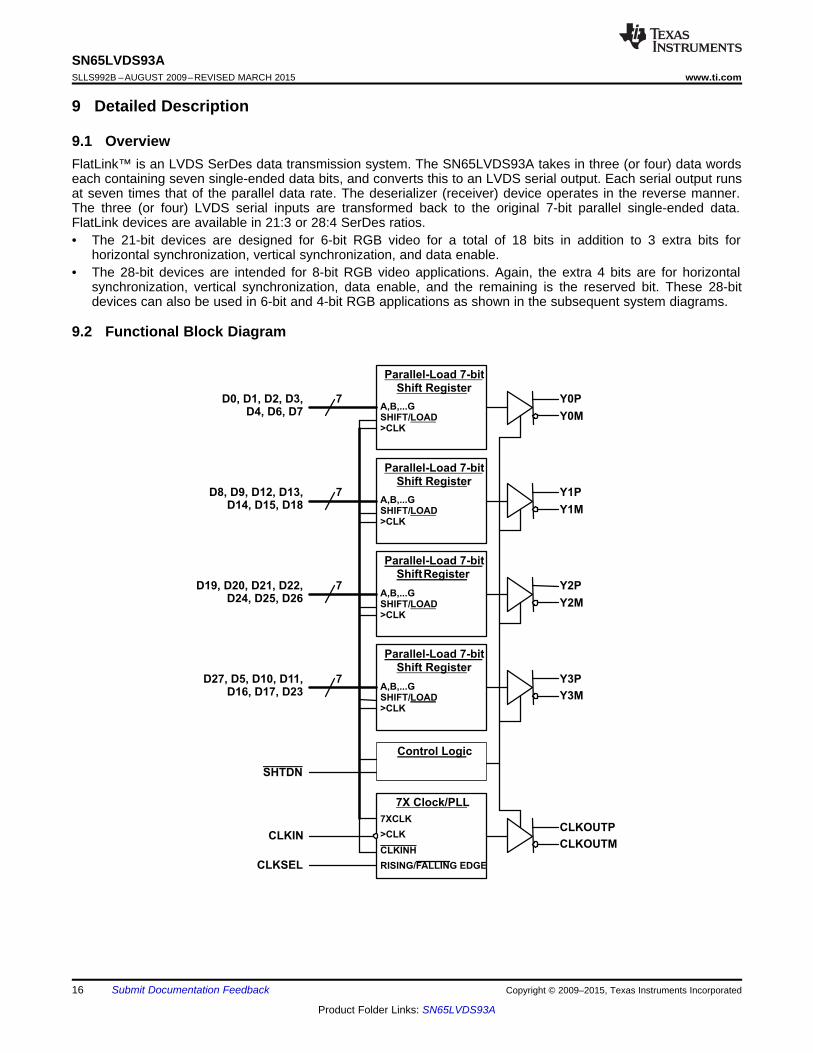
9 Detailed Description
9.1 OverviewFlatLink™ is an LVDS SerDes data transmission system. The SN65LVDS93A takes in three (or four) data wordseach containing seven single-ended data bits, and converts this to an LVDS serial output. Each serial output runsat seven times that of the parallel data rate. The deserializer (receiver) device operates in the reverse manner.The three (or four) LVDS serial inputs are transformed back to the original 7-bit parallel single-ended data.FlatLink devices are available in 21:3 or 28:4 SerDes ratios.• The 21-bit devices are designed for 6-bit RGB video for a total of 18 bits in addition to 3 extra bits for
horizontal synchronization, vertical synchronization, and data enable.• The 28-bit devices are intended for 8-bit RGB video applications. Again, the extra 4 bits are for horizontal
synchronization, vertical synchronization, data enable, and the remaining is the reserved bit. These 28-bitdevices can also be used in 6-bit and 4-bit RGB applications as shown in the subsequent system diagrams.
9.2 Functional Block Diagram
16 Submit Documentation Feedback Copyright © 2009–2015, Texas Instruments Incorporated
Product Folder Links: SN65LVDS93A
SN65LVDS93Awww.ti.com SLLS992B –AUGUST 2009–REVISED MARCH 2015
9.3 Feature Description
9.3.1 TTL Input DataThe data inputs to the transmitter come from the graphics processor and consist of up to 24 bits of videoinformation, a horizontal synchronization bit, a vertical synchronization bit, an enable bit, and a spare bit. Thedata can be loaded into the registers upon either the rising or falling edge of the input clock selectable by theCLKSEL pin. Data inputs are 1.8 V to 3.3 V tolerant for the SN65LVDS93A and can connect directly to low-power, low-voltage application and graphic processors. The bit mapping is listed in Table 1.
Table 1. Pixel Bit OrderingRED GREEN BLUE
LSB R0 G0 B0R1 G1 B1R2 G2 B2
4-bit MSB R3 G3 B3R4 G4 B4
6-bit MSB R5 G5 B5R6 G6 B6
8-bit MSB R7 G7 B7
9.3.2 LVDS Output DataThe pixel data assignment is listed in Table 2 for 24-bit, 18-bit, and 12-bit color hosts.
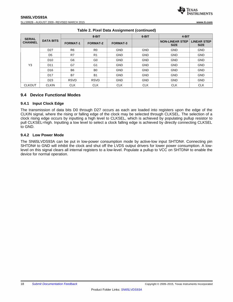
Table 2. Pixel Data Assignment8-BIT 6-BIT 4-BIT
SERIAL DATA BITS NON-LINEAR STEP LINEAR STEPCHANNEL FORMAT-1 FORMAT-2 FORMAT-3 SIZE SIZED0 R0 R2 R2 R0 R2 VCCD1 R1 R3 R3 R1 R3 GNDD2 R2 R4 R4 R2 R0 R0
Y0 D3 R3 R5 R5 R3 R1 R1D4 R4 R6 R6 R4 R2 R2D6 R5 R7 R7 R5 R3 R3D7 G0 G2 G2 G0 G2 VCCD8 G1 G3 G3 G1 G3 GNDD9 G2 G4 G4 G2 G0 G0
D12 G3 G5 G5 G3 G1 G1Y1 D13 G4 G6 G6 G4 G2 G2
D14 G5 G7 G7 G5 G3 G3D15 B0 B2 B2 B0 B2 VCCD18 B1 B3 B3 B1 B3 GNDD19 B2 B4 B4 B2 B0 B0D20 B3 B5 B5 B3 B1 B1D21 B4 B6 B6 B4 B2 B2
Y2 D22 B5 B7 B7 B5 B3 B3D24 HSYNC HSYNC HSYNC HSYNC HSYNC HSYNCD25 VSYNC VSYNC VSYNC VSYNC VSYNC VSYNCD26 ENABLE ENABLE ENABLE ENABLE ENABLE ENABLE
Copyright © 2009–2015, Texas Instruments Incorporated Submit Documentation Feedback 17
Product Folder Links: SN65LVDS93A
SN65LVDS93ASLLS992B –AUGUST 2009–REVISED MARCH 2015 www.ti.com
Table 2. Pixel Data Assignment (continued)8-BIT 6-BIT 4-BIT
SERIAL DATA BITS NON-LINEAR STEP LINEAR STEPCHANNEL FORMAT-1 FORMAT-2 FORMAT-3 SIZE SIZED27 R6 R0 GND GND GND GNDD5 R7 R1 GND GND GND GND
D10 G6 G0 GND GND GND GNDY3 D11 G7 G1 GND GND GND GND
D16 B6 B0 GND GND GND GNDD17 B7 B1 GND GND GND GNDD23 RSVD RSVD GND GND GND GND
CLKOUT CLKIN CLK CLK CLK CLK CLK CLK
9.4 Device Functional Modes
9.4.1 Input Clock EdgeThe transmission of data bits D0 through D27 occurs as each are loaded into registers upon the edge of theCLKIN signal, where the rising or falling edge of the clock may be selected through CLKSEL. The selection of aclock rising edge occurs by inputting a high level to CLKSEL, which is achieved by populating pullup resistor topull CLKSEL=high. Inputting a low level to select a clock falling edge is achieved by directly connecting CLKSELto GND.
9.4.2 Low Power ModeThe SN65LVDS93A can be put in low-power consumption mode by active-low input SHTDN#. Connecting pinSHTDN# to GND will inhibit the clock and shut off the LVDS output drivers for lower power consumption. A low-level on this signal clears all internal registers to a low-level. Populate a pullup to VCC on SHTDN# to enable thedevice for normal operation.
18 Submit Documentation Feedback Copyright © 2009–2015, Texas Instruments Incorporated
Product Folder Links: SN65LVDS93A
SN65LVDS93Awww.ti.com SLLS992B –AUGUST 2009–REVISED MARCH 2015
10 Application and Implementation
NOTEInformation in the following applications sections is not part of the TI componentspecification, and TI does not warrant its accuracy or completeness. TI’s customers areresponsible for determining suitability of components for their purposes. Customers shouldvalidate and test their design implementation to confirm system functionality.
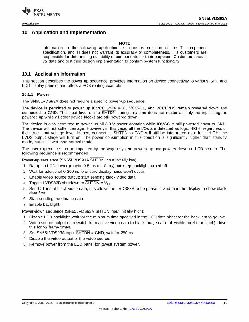
10.1 Application InformationThis section describes the power up sequence, provides information on device connectivity to various GPU andLCD display panels, and offers a PCB routing example.
10.1.1 PowerThe SN65LVDS93A does not require a specific power-up sequence.
The device is permitted to power up IOVCC while VCC, VCCPLL, and VCCLVDS remain powered down andconnected to GND. The input level of the SHTDN during this time does not matter as only the input stage ispowered up while all other device blocks are still powered down.
The device is also permitted to power up all 3.3-V power domains while IOVCC is still powered down to GND.The device will not suffer damage. However, in this case, all the I/Os are detected as logic HIGH, regardless oftheir true input voltage level. Hence, connecting SHTDN to GND will still be interpreted as a logic HIGH; theLVDS output stage will turn on. The power consumption in this condition is significantly higher than standbymode, but still lower than normal mode.
The user experience can be impacted by the way a system powers up and powers down an LCD screen. Thefollowing sequence is recommended:
Power-up sequence (SN65LVDS93A SHTDN input initially low):1. Ramp up LCD power (maybe 0.5 ms to 10 ms) but keep backlight turned off.2. Wait for additional 0-200ms to ensure display noise won’t occur.3. Enable video source output; start sending black video data.4. Toggle LVDS83B shutdown to SHTDN = VIH.5. Send >1 ms of black video data; this allows the LVDS83B to be phase locked, and the display to show black
data first.6. Start sending true image data.7. Enable backlight.
Power-down sequence (SN65LVDS93A SHTDN input initially high):1. Disable LCD backlight; wait for the minimum time specified in the LCD data sheet for the backlight to go low.2. Video source output data switch from active video data to black image data (all visible pixel turn black); drive
this for >2 frame times.3. Set SN65LVDS93A input SHTDN = GND; wait for 250 ns.4. Disable the video output of the video source.5. Remove power from the LCD panel for lowest system power.
Copyright © 2009–2015, Texas Instruments Incorporated Submit Documentation Feedback 19
Product Folder Links: SN65LVDS93A
J2
J8
J9
J7
J10
sma_surface
sma_surface
J6
J5
J1
SN65LVDS93A-Q1ZQL
U1A
Y3MC1
Y3PC2
CLKMD1
CLKPD2
Y2PE1
Y2ME2
Y1MG1
Y1PG2
Y0MH1
Y0PH2
J4
J3
R5
4.7k
SN65LVDS93A-Q1ZQL
U1B
D0J2
D3J3
D6J4
D1K1
D2K2
D4K3
D7K5
R21
4.7k
R8
4.7k
R6
4.7k
JMP1
Header 7x2
1 2
14
R26
4.7k
R16
4.7k
R22
4.7k
R9
4.7k
R7
4.7k
R27
4.7k
SN65LVDS93A-Q1ZQL
U1C
D18D5
D15E5
D14F6
D12G5
D13G6
D9J6
D8K6
R17
4.7k
R23
4.7k
R10
4.7k
R11
4.7k
JMP4
Header 7x2
1 2
14
R28
4.7k
R24
4.7k
R12
4.7k
SN65LVDS93A-Q1ZQL
U1D
D26A3
D24A4
D22A6
D25B4
D21B5
D20B6
D19C6
R18
4.7k
JMP2
Header 7x2
1 2
14
R29
4.7k
R13
4.7k
R19
4.7k
R30
4.7k
SN65LVDS93A-Q1ZQL
U1E
D23A5
D17D6
D16E6
D10H4
D11H6
D27J1
D5K4
R14
4.7k
JMP3
Header 7x2
1 2
14
R20
4.7k
R31
4.7k
R25
4.7k
R4
4.7k
R15
4.7k
D2
D1
D6
D0
D7
D3
D4
D8
D9
D14
D13
D12
D18
D19
D22
D26
D21
D24
D25
D20
D5
D11
D27
D10
D23
D17
D16
D15
IOVCC
IOVCC
IOVCC
IOVCC
SN65LVDS93A-Q1ZQL
U1I
PLLVCCB2
IOVCC2C4
LVDSVCCF1
VCCG4
IOVCC1H5
VCC IOVCC
SN65LVDS93A-Q1ZQL
U1H
PLLGNDA1
LVDSGND1B1
GND1C3
GND2C5
GND3D3
LVDSGND2F2
GND4F5
GND5G3
GND6H3
GND7J5
U1J
SN65LVDS93A-Q1ZQL
NC1E3
NC2E4
NC3F3
NC4F4
R2
SN65LVDS93A-Q1ZQL
U1G
SHTDNB3
CLKSELD4
JMP6
Header 2x2
1 2
3 4
R1
4.7k
SHTDN
CLKSEL
IOVCC IOVCC
C360.01uF
C39
0.01uF
C40
1uF
C330.01uF
C41
0.1uF
C320.1uF
C311uF
C42
0.01uF
C341uF
C37
1uF
C350.1uF
C38
0.1uF
VCC VCCVCC IOVCC
PLACE UNDER LVDS93A-Q1(bottom pcb side)
sma_surface
sma_surface
sma_surface
sma_surface
sma_surface
sma_surface
sma_surface
sma_surface
SN65LVDS93ASLLS992B –AUGUST 2009–REVISED MARCH 2015 www.ti.com
10.2 Typical Application
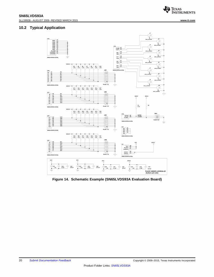
Figure 14. Schematic Example (SN65LVDS93A Evaluation Board)
20 Submit Documentation Feedback Copyright © 2009–2015, Texas Instruments Incorporated
Product Folder Links: SN65LVDS93A
SN65LVDS93Awww.ti.com SLLS992B –AUGUST 2009–REVISED MARCH 2015
Typical Application (continued)10.2.1 Design RequirementsFor this design example, use the parameters listed in Table 3 as the input parameters.
Table 3. Design ParametersDESIGN PARAMETER EXAMPLE VALUE
VCC 3.3 VVCCIO 1.8 VCLKIN Falling edge
SHTDN# HighFormat 18-bit GPU to 24-bit LCD
10.2.2 Detailed Design Procedure
10.2.2.1 Signal ConnectivityWhile there is no formal industry standardized specification for the input interface of LVDS LCD panels, theindustry has aligned over the years on a certain data format (bit order). Figure 15 through Figure 18 show howeach signal should be connected from the graphic source through the SN65LVDS93A input, output and LVDSLCD panel input. Detailed notes are provided with each figure.
Copyright © 2009–2015, Texas Instruments Incorporated Submit Documentation Feedback 21
Product Folder Links: SN65LVDS93A
SN65LVDS93A24-bpc GPU
R0(LSB)
R1
R2
R3
R4
R5
R6
R7(MSB)
G0(LSB)
G1
G2
G3
G4
G5
G6
G7(MSB)
B0(LSB)
B1
B2
B3
B4
B5
B6
B7(MSB)
HSYNC
VSYNC
ENABLE
RSVD (Note C)
CLK
FORMAT1
D0
D1
D2
D3
D4
D6
D27
D5
D7
D8
D9
D12
D13
D14
D10
D11
D15
D18
D19
D20
D21
D22
D16
D17
D24
D25
D26
D23
CLKIN
Y0M
Y0P
Y1M
Y1P
Y2M
Y2P
Y3M
Y3P
CLKOUTM
CLKOUTP
FPC
Cable
VD
DG
PUIO
1.8V or 2.5Vor 3.3V
GN
D
C1
100LVDStiming
Controller(8bpc, 24bpp)
100
100
100
100
to columndriver
to row driver
Main Board
IOV
CC
CLK
SE
L
Rpullup
Rpulldown
(See Note B)
VC
C
LV
DS
VC
CP
LLV
CC
GN
D
3.3V
C2 C3
3.3V
SH
TD
N
4.8k
24-bpp LCD Display
FORMAT2 (See Note A)
D27
D5
D0
D1
D2
D3
D4
D6
D10
D11
D7
D8
D9
D12
D13
D14
D16
D17
D15
D18
D19
D20
D21
D22
D24
D25
D26
D23
CLKIN
Pa
ne
l co
nn
ecto
r
Ma
in b
oa
rd c
on
ne
cto
r
SN65LVDS93ASLLS992B –AUGUST 2009–REVISED MARCH 2015 www.ti.com
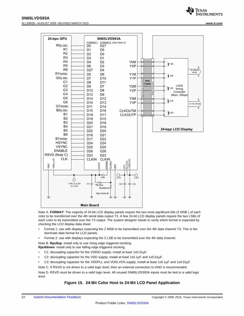
Note A. FORMAT: The majority of 24-bit LCD display panels require the two most significant bits (2 MSB ) of eachcolor to be transferred over the 4th serial data output Y3. A few 24-bit LCD display panels require the two LSBs ofeach color to be transmitted over the Y3 output. The system designer needs to verify which format is expected bychecking the LCD display data sheet.• Format 1: use with displays expecting the 2 MSB to be transmitted over the 4th data channel Y3. This is the
dominate data format for LCD panels.• Format 2: use with displays expecting the 2 LSB to be transmitted over the 4th data channel.Note B. Rpullup: install only to use rising edge triggered clocking.Rpulldown: install only to use falling edge triggered clocking.• C1: decoupling capacitor for the VDDIO supply; install at least 1x0.01µF.• C2: decoupling capacitor for the VDD supply; install at least 1x0.1µF and 1x0.01µF.• C3: decoupling capacitor for the VDDPLL and VDDLVDS supply; install at least 1x0.1µF and 1x0.01µF.Note C. If RSVD is not driven to a valid logic level, then an external connection to GND is recommended.Note D. RSVD must be driven to a valid logic level. All unused SN65LVDS93A inputs must be tied to a valid logiclevel.
Figure 15. 24-Bit Color Host to 24-Bit LCD Panel Application
22 Submit Documentation Feedback Copyright © 2009–2015, Texas Instruments Incorporated
Product Folder Links: SN65LVDS93A
SN65LVDS93A18-bpp GPU
R0(LSB)
R1
R2
R3
R4
R5(MSB)
G0(LSB)
G1
G2
G3
G4
G5(MSB)
B0(LSB)
B1
B2
B3
B4
B5(MSB)
HSYNC
VSYNC
ENABLE
RSVD
CLK
D0
D1
D2
D3
D4
D6
D27
D5
D7
D8
D9
D12
D13
D14
D10
D11
D15
D18
D19
D20
D21
D22
D16
D17
D24
D25
D26
D23
CLKIN
Y0M
Y0P
Y1M
Y1P
Y2M
Y2P
CLKOUTM
CLKOUTP
(See Note A)
(See Note B)
Y3M
Y3P
FPC
Cable
VD
DG
PUIO
1.8V or 2.5Vor 3.3V
GN
D
IOV
CC
CLK
SE
L
Rpullup
Rpulldown
VC
C
LVD
SV
CC
PLLV
CC
GN
D
3.3V
C2C1 C3
3.3V
100LVDStiming
Controller(6-bpc, 18-bpp)
100
100
100
to column
driver
to row driver
Main Board
SH
TD
N
4.8k
18-bpp LCD Display
Pa
ne
l co
nn
ecto
r
Ma
in b
oa
rd c
on
ne
cto
r
SN65LVDS93Awww.ti.com SLLS992B –AUGUST 2009–REVISED MARCH 2015
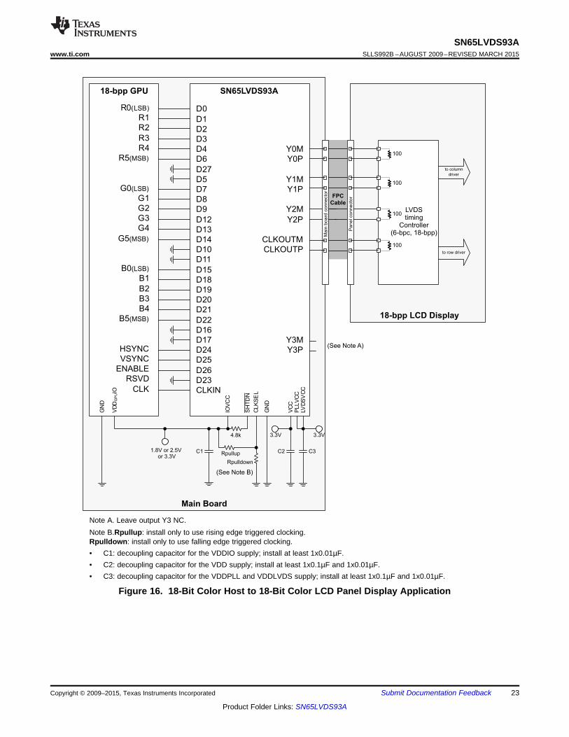
Note A. Leave output Y3 NC.Note B.Rpullup: install only to use rising edge triggered clocking.Rpulldown: install only to use falling edge triggered clocking.• C1: decoupling capacitor for the VDDIO supply; install at least 1x0.01µF.• C2: decoupling capacitor for the VDD supply; install at least 1x0.1µF and 1x0.01µF.• C3: decoupling capacitor for the VDDPLL and VDDLVDS supply; install at least 1x0.1µF and 1x0.01µF.
Figure 16. 18-Bit Color Host to 18-Bit Color LCD Panel Display Application
Copyright © 2009–2015, Texas Instruments Incorporated Submit Documentation Feedback 23
Product Folder Links: SN65LVDS93A
SN65LVDS93A12-bpp GPU
R2 or VCC
R3 or GND
R0
R1
R2
R3(MSB)
G2 or VCC
G3 or GND
G0
G1
G2
G3(MSB)
B2 or VCC
B3 or GND
B0
B1
B2
B3(MSB)
HSYNC
VSYNC
ENABLE
RSVD
CLK
D0
D1
D2
D3
D4
D6
D27
D5
D7
D8
D9
D12
D13
D14
D10
D11
D15
D18
D19
D20
D21
D22
D16
D17
D24
D25
D26
D23
CLKIN
Y0M
Y0P
Y1M
Y1P
Y2M
Y2P
CLKOUTM
CLKOUTP
Y3M
Y3P
FPC
Cable
VD
DG
PUIO
1.8V or 2.5Vor 3.3V
GN
D
IOV
CC
CLK
SE
L
Rpullup
Rpulldown
(See Note C)
(See Note A)
VC
C
LVD
SV
CC
PLLV
CC
GN
D
3.3V
C2C1 C3
3.3V
100LVDStiming
Controller(6-bpc, 18-bpp)
lt
100
100
100
to columndriver
to row driver
Main Board
18-bpp LCD Display
SH
TD
N
4.8k
Pa
ne
l co
nn
ecto
r
Ma
in b
oa
rd c
on
ne
cto
r
(See Note B)
(See Note B)
(See Note B)
SN65LVDS93ASLLS992B –AUGUST 2009–REVISED MARCH 2015 www.ti.com
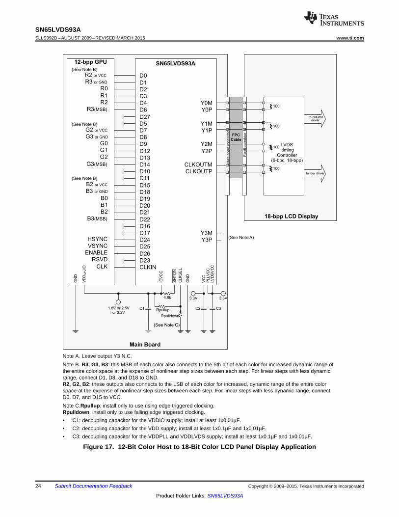
Note A. Leave output Y3 N.C.Note B. R3, G3, B3: this MSB of each color also connects to the 5th bit of each color for increased dynamic range ofthe entire color space at the expense of nonlinear step sizes between each step. For linear steps with less dynamicrange, connect D1, D8, and D18 to GND.R2, G2, B2: these outputs also connects to the LSB of each color for increased, dynamic range of the entire colorspace at the expense of nonlinear step sizes between each step. For linear steps with less dynamic range, connectD0, D7, and D15 to VCC.Note C.Rpullup: install only to use rising edge triggered clocking.Rpulldown: install only to use falling edge triggered clocking.• C1: decoupling capacitor for the VDDIO supply; install at least 1x0.01µF.• C2: decoupling capacitor for the VDD supply; install at least 1x0.1µF and 1x0.01µF.• C3: decoupling capacitor for the VDDPLL and VDDLVDS supply; install at least 1x0.1µF and 1x0.01µF.
Figure 17. 12-Bit Color Host to 18-Bit Color LCD Panel Display Application
24 Submit Documentation Feedback Copyright © 2009–2015, Texas Instruments Incorporated
Product Folder Links: SN65LVDS93A
SN65LVDS93A24-bpp GPU
R2
R3
R4
R5
R6
R7(MSB)
G2
G3
G4
G5
G6
G7(MSB)
B2
B3
B4
B5
B6
B7(MSB)
HSYNC
VSYNC
ENABLE
RSVD
CLK
D0
D1
D2
D3
D4
D6
D27
D5
D7
D8
D9
D12
D13
D14
D10
D11
D15
D18
D19
D20
D21
D22
D16
D17
D24
D25
D26
D23
CLKIN
Y0M
Y0P
Y1M
Y1P
Y2M
Y2P
CLKOUTM
CLKOUTP
Y3M
Y3P
FPC
Cable
VD
DG
PUIO
1.8V or 2.5Vor 3.3V
GN
D
IOV
CC
CLK
SE
L
Rpullup
Rpulldown
(See Note C)
(See Note A)
VC
C
LVD
SV
CC
PLLV
CC
GN
D
3.3V
C2C1 C3
3.3V
100LVDStiming
Controller(6-bpc, 18-bpp)
lt
100
100
100
to columndriver
to row driver
Main Board
18-bpp LCD Display
SH
TD
N
4.8k
Pa
ne
l co
nn
ecto
r
Ma
in b
oa
rd c
on
ne
cto
r
R0 and R1: NC(See Note B)
B0 and B1: NC(See Note B)
G0 and G1: NC(See Note B)
B0 and B1: NC(See Note B)
SN65LVDS93Awww.ti.com SLLS992B –AUGUST 2009–REVISED MARCH 2015
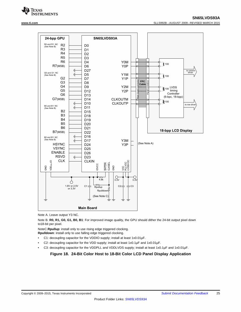
Note A. Leave output Y3 NC.Note B. R0, R1, G0, G1, B0, B1: For improved image quality, the GPU should dither the 24-bit output pixel downto18-bit per pixel.NoteC.Rpullup: install only to use rising edge triggered clocking.Rpulldown: install only to use falling edge triggered clocking.• C1: decoupling capacitor for the VDDIO supply; install at least 1x0.01µF.• C2: decoupling capacitor for the VDD supply; install at least 1x0.1µF and 1x0.01µF.• C3: decoupling capacitor for the VDDPLL and VDDLVDS supply; install at least 1x0.1µF and 1x0.01µF.
Figure 18. 24-Bit Color Host to 18-Bit Color LCD Panel Display Application
Copyright © 2009–2015, Texas Instruments Incorporated Submit Documentation Feedback 25
Product Folder Links: SN65LVDS93A
Pixel Samples
Pix
el V
alu
e (
de
c)
1 4 7 10 13
0
200
250
150
100
50
16 19 2219 25 28 31 34 37 40 43 46 49 52 55 58 61 64
D27
D5
D10
D11
D16
D17
D23
D19
D20
D21
D22
D24
D25
D26
D8
D9
D12
D13
D14
D15
D18
D0
D1
D2
D3
D4
D6
D7
CLKIN
Y0M
Y0P
Y1M
Y1P
Y2M
Y2P
CLKINM
CLKINP
Y3M
Y3P
SN65LVDS93ASLLS992B –AUGUST 2009–REVISED MARCH 2015 www.ti.com
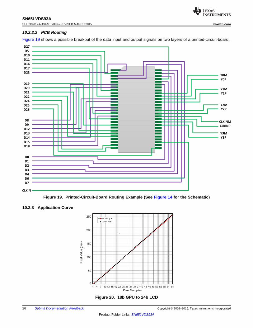
10.2.2.2 PCB RoutingFigure 19 shows a possible breakout of the data input and output signals on two layers of a printed-circuit-board.
Figure 19. Printed-Circuit-Board Routing Example (See Figure 14 for the Schematic)
10.2.3 Application Curve
Figure 20. 18b GPU to 24b LCD
26 Submit Documentation Feedback Copyright © 2009–2015, Texas Instruments Incorporated
Product Folder Links: SN65LVDS93A
SN65LVDS93Awww.ti.com SLLS992B –AUGUST 2009–REVISED MARCH 2015
11 Power Supply Recommendations
Power supply PLL, IO, and LVDS pins must be uncoupled from each.
12 Layout
12.1 Layout Guidelines
12.1.1 Board StackupThere is no fundamental information about how many layers should be used and how the board stackup shouldlook. Again, the easiest way the get good results is to use the design from the EVMs of TI. The magazineElektronik Praxis has published an article with an analysis of different board stackups. These are listed inTable 4. Generally, the use of microstrip traces needs at least two layers, whereas one of them must be a GNDplane. Better is the use of a 4-layer PCB, with a GND and a VCC plane and two signal layers. If the circuit iscomplex and signals must be routed as stripline, because of propagation delay and/or characteristic impedance,a 6-layer stackup should be used.
Table 4. Possible Board Stackup on a Four-Layer PCBMODEL 1 MODEL 2 MODEL 3 MODEL 4
Layer 1 SIG SIG SIG GNDLayer 2 SIG GND GND SIGLayer 3 VCC VCC SIG VCCLayer 4 GND SIG VCC SIG
Decoupling Good Good Bad BadEMC Bad Bad Bad Bad
Signal Integrity Bad Bad Good BadSelf Disturbance Satisfaction Satisfaction Satisfaction High
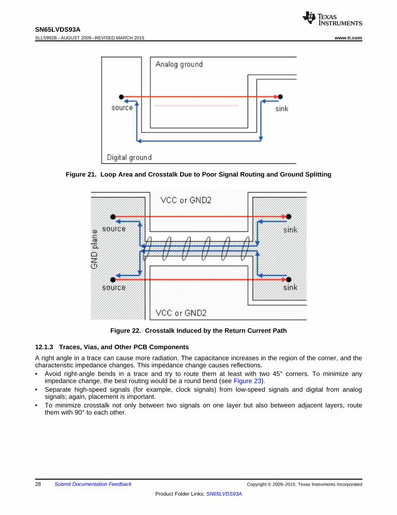
12.1.2 Power and Ground PlanesA complete ground plane in high-speed design is essential. Additionally, a complete power plane isrecommended as well. In a complex system, several regulated voltages can be present. The best solution is forevery voltage to have its own layer and its own ground plane. But this would result in a huge number of layersjust for ground and supply voltages. What are the alternatives? Split the ground planes and the power planes? Ina mixed-signal design, for example, using data converters, the manufacturer often recommends splitting theanalog ground and the digital ground to avoid noise coupling between the digital part and the sensitive analogpart. Take care when using split ground planes because:• Split ground planes act as slot antennas and radiate.• A routed trace over a gap creates large loop areas, because the return current cannot flow beside the signal,
and the signal can induce noise into the nonrelated reference plane (Figure 21).• With a proper signal routing, crosstalk also can arise in the return current path due to discontinuities in the
ground plane. Always take care of the return current (Figure 22).
For Figure 22, do not route a signal referenced to digital ground over analog ground and vice versa. The returncurrent cannot take the direct way along the signal trace and so a loop area occurs. Furthermore, the signalinduces noise, due to crosstalk (dotted red line) into the analog ground plane.
Copyright © 2009–2015, Texas Instruments Incorporated Submit Documentation Feedback 27
Product Folder Links: SN65LVDS93A
SN65LVDS93ASLLS992B –AUGUST 2009–REVISED MARCH 2015 www.ti.com
Figure 21. Loop Area and Crosstalk Due to Poor Signal Routing and Ground Splitting
Figure 22. Crosstalk Induced by the Return Current Path
12.1.3 Traces, Vias, and Other PCB ComponentsA right angle in a trace can cause more radiation. The capacitance increases in the region of the corner, and thecharacteristic impedance changes. This impedance change causes reflections.• Avoid right-angle bends in a trace and try to route them at least with two 45° corners. To minimize any
impedance change, the best routing would be a round bend (see Figure 23).• Separate high-speed signals (for example, clock signals) from low-speed signals and digital from analog
signals; again, placement is important.• To minimize crosstalk not only between two signals on one layer but also between adjacent layers, route
them with 90° to each other.
28 Submit Documentation Feedback Copyright © 2009–2015, Texas Instruments Incorporated
Product Folder Links: SN65LVDS93A
SN
65LV
DS
93A
-Q1
EV
M R
EV
6507548
SN65LVDS93Awww.ti.com SLLS992B –AUGUST 2009–REVISED MARCH 2015
Figure 23. Poor and Good Right-Angle Bends
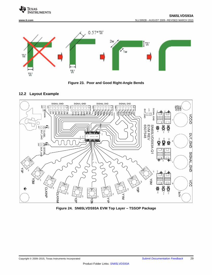
12.2 Layout Example
Figure 24. SN65LVDS93A EVM Top Layer – TSSOP Package
Copyright © 2009–2015, Texas Instruments Incorporated Submit Documentation Feedback 29
Product Folder Links: SN65LVDS93A
SN65LVDS93ASLLS992B –AUGUST 2009–REVISED MARCH 2015 www.ti.com
Layout Example (continued)
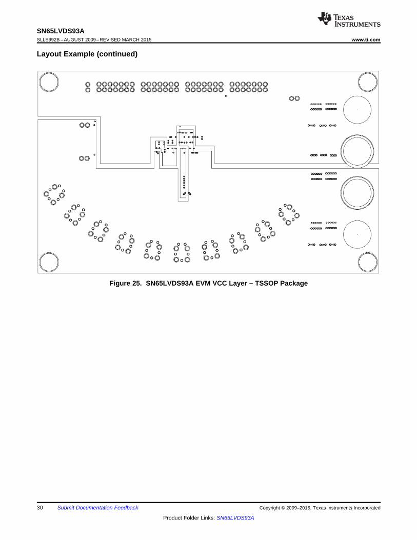
Figure 25. SN65LVDS93A EVM VCC Layer – TSSOP Package
30 Submit Documentation Feedback Copyright © 2009–2015, Texas Instruments Incorporated
Product Folder Links: SN65LVDS93A
SN65LVDS93Awww.ti.com SLLS992B –AUGUST 2009–REVISED MARCH 2015
13 Device and Documentation Support
13.1 Documentation Support
13.1.1 Related DocumentationFor related documentation see the following:
LVDS SerDes Receiver, SLLS928
13.2 TrademarksOMAP, DaVinci, FlatLink are trademarks of Texas Instruments.All other trademarks are the property of their respective owners.
13.3 Electrostatic Discharge CautionThese devices have limited built-in ESD protection. The leads should be shorted together or the device placed in conductive foamduring storage or handling to prevent electrostatic damage to the MOS gates.
13.4 GlossarySLYZ022 — TI Glossary.
This glossary lists and explains terms, acronyms, and definitions.
14 Mechanical, Packaging, and Orderable InformationThe following pages include mechanical, packaging, and orderable information. This information is the mostcurrent data available for the designated devices. This data is subject to change without notice and revision ofthis document. For browser-based versions of this data sheet, refer to the left-hand navigation.
Copyright © 2009–2015, Texas Instruments Incorporated Submit Documentation Feedback 31
Product Folder Links: SN65LVDS93A
PACKAGE OPTION ADDENDUM
www.ti.com 19-Mar-2015
Addendum-Page 1
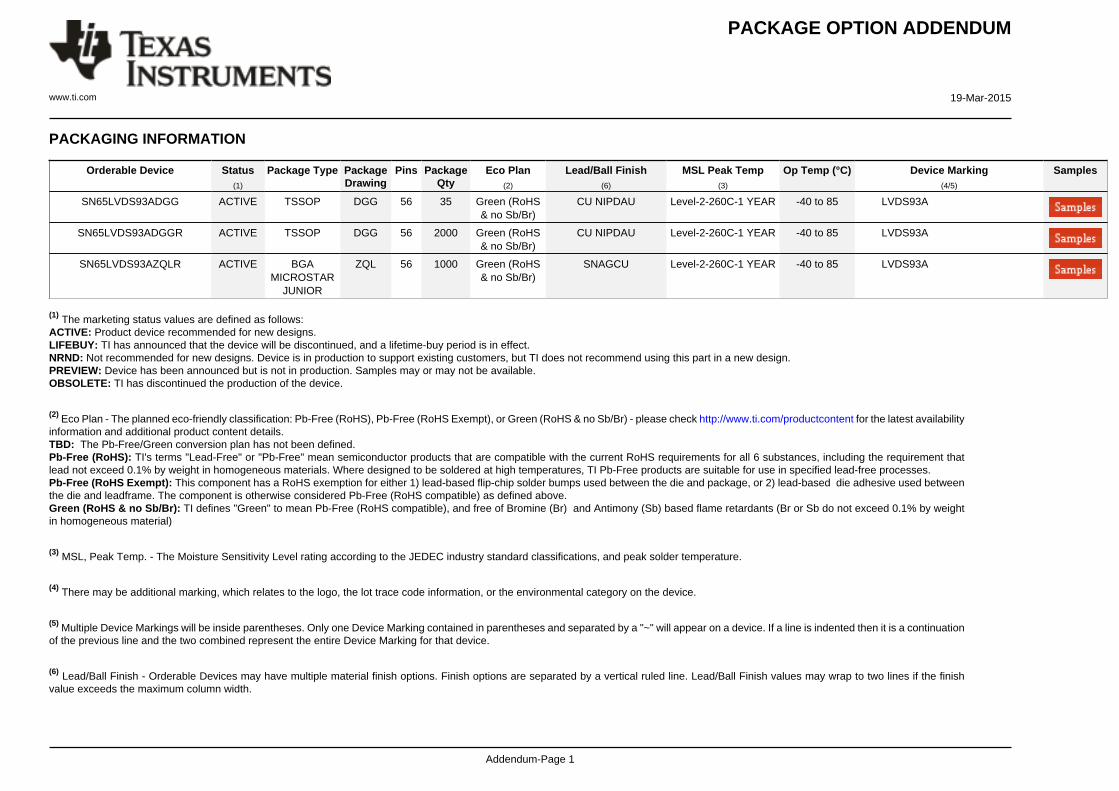
PACKAGING INFORMATION
Orderable Device Status(1)
Package Type PackageDrawing
Pins PackageQty
Eco Plan(2)
Lead/Ball Finish(6)
MSL Peak Temp(3)
Op Temp (°C) Device Marking(4/5)
Samples
SN65LVDS93ADGG ACTIVE TSSOP DGG 56 35 Green (RoHS& no Sb/Br)
CU NIPDAU Level-2-260C-1 YEAR -40 to 85 LVDS93A
SN65LVDS93ADGGR ACTIVE TSSOP DGG 56 2000 Green (RoHS& no Sb/Br)
CU NIPDAU Level-2-260C-1 YEAR -40 to 85 LVDS93A
SN65LVDS93AZQLR ACTIVE BGAMICROSTAR
JUNIOR
ZQL 56 1000 Green (RoHS& no Sb/Br)
SNAGCU Level-2-260C-1 YEAR -40 to 85 LVDS93A
(1) The marketing status values are defined as follows:ACTIVE: Product device recommended for new designs.LIFEBUY: TI has announced that the device will be discontinued, and a lifetime-buy period is in effect.NRND: Not recommended for new designs. Device is in production to support existing customers, but TI does not recommend using this part in a new design.PREVIEW: Device has been announced but is not in production. Samples may or may not be available.OBSOLETE: TI has discontinued the production of the device.
(2) Eco Plan - The planned eco-friendly classification: Pb-Free (RoHS), Pb-Free (RoHS Exempt), or Green (RoHS & no Sb/Br) - please check http://www.ti.com/productcontent for the latest availabilityinformation and additional product content details.TBD: The Pb-Free/Green conversion plan has not been defined.Pb-Free (RoHS): TI's terms "Lead-Free" or "Pb-Free" mean semiconductor products that are compatible with the current RoHS requirements for all 6 substances, including the requirement thatlead not exceed 0.1% by weight in homogeneous materials. Where designed to be soldered at high temperatures, TI Pb-Free products are suitable for use in specified lead-free processes.Pb-Free (RoHS Exempt): This component has a RoHS exemption for either 1) lead-based flip-chip solder bumps used between the die and package, or 2) lead-based die adhesive used betweenthe die and leadframe. The component is otherwise considered Pb-Free (RoHS compatible) as defined above.Green (RoHS & no Sb/Br): TI defines "Green" to mean Pb-Free (RoHS compatible), and free of Bromine (Br) and Antimony (Sb) based flame retardants (Br or Sb do not exceed 0.1% by weightin homogeneous material)
(3) MSL, Peak Temp. - The Moisture Sensitivity Level rating according to the JEDEC industry standard classifications, and peak solder temperature.
(4) There may be additional marking, which relates to the logo, the lot trace code information, or the environmental category on the device.
(5) Multiple Device Markings will be inside parentheses. Only one Device Marking contained in parentheses and separated by a "~" will appear on a device. If a line is indented then it is a continuationof the previous line and the two combined represent the entire Device Marking for that device.
(6) Lead/Ball Finish - Orderable Devices may have multiple material finish options. Finish options are separated by a vertical ruled line. Lead/Ball Finish values may wrap to two lines if the finishvalue exceeds the maximum column width.
PACKAGE OPTION ADDENDUM
www.ti.com 19-Mar-2015
Addendum-Page 2
Important Information and Disclaimer:The information provided on this page represents TI's knowledge and belief as of the date that it is provided. TI bases its knowledge and belief on informationprovided by third parties, and makes no representation or warranty as to the accuracy of such information. Efforts are underway to better integrate information from third parties. TI has taken andcontinues to take reasonable steps to provide representative and accurate information but may not have conducted destructive testing or chemical analysis on incoming materials and chemicals.TI and TI suppliers consider certain information to be proprietary, and thus CAS numbers and other limited information may not be available for release.
In no event shall TI's liability arising out of such information exceed the total purchase price of the TI part(s) at issue in this document sold by TI to Customer on an annual basis.
OTHER QUALIFIED VERSIONS OF SN65LVDS93A :
• Automotive: SN65LVDS93A-Q1
NOTE: Qualified Version Definitions:
• Automotive - Q100 devices qualified for high-reliability automotive applications targeting zero defects
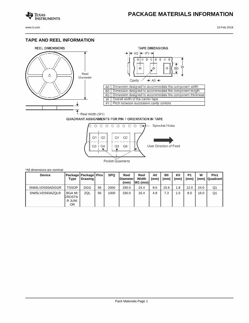
TAPE AND REEL INFORMATION
*All dimensions are nominal
Device PackageType
PackageDrawing
Pins SPQ ReelDiameter
(mm)
ReelWidth
W1 (mm)
A0(mm)
B0(mm)
K0(mm)
P1(mm)
W(mm)
Pin1Quadrant
SN65LVDS93ADGGR TSSOP DGG 56 2000 330.0 24.4 8.6 15.6 1.8 12.0 24.0 Q1
SN65LVDS93AZQLR BGA MI CROSTA
R JUNI OR
ZQL 56 1000 330.0 16.4 4.8 7.3 1.5 8.0 16.0 Q1
PACKAGE MATERIALS INFORMATION
www.ti.com 10-Feb-2018
Pack Materials-Page 1
*All dimensions are nominal
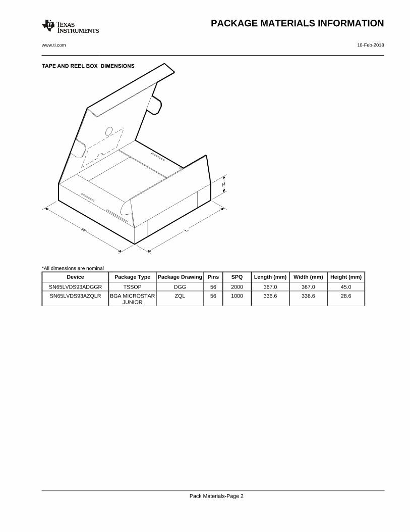
Device Package Type Package Drawing Pins SPQ Length (mm) Width (mm) Height (mm)
SN65LVDS93ADGGR TSSOP DGG 56 2000 367.0 367.0 45.0
SN65LVDS93AZQLR BGA MICROSTARJUNIOR
ZQL 56 1000 336.6 336.6 28.6
PACKAGE MATERIALS INFORMATION
www.ti.com 10-Feb-2018
Pack Materials-Page 2
www.ti.com
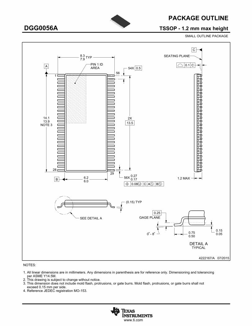
PACKAGE OUTLINE
C
TYP8.37.9
1.2 MAX
54X 0.5
56X 0.270.17
2X13.5
(0.15) TYP
0 - 80.150.05
0.25GAGE PLANE
0.750.50
A
NOTE 3
14.113.9
B 6.26.0
4222167/A 07/2015
TSSOP - 1.2 mm max heightDGG0056ASMALL OUTLINE PACKAGE
NOTES: 1. All linear dimensions are in millimeters. Any dimensions in parenthesis are for reference only. Dimensioning and tolerancing per ASME Y14.5M. 2. This drawing is subject to change without notice. 3. This dimension does not include mold flash, protrusions, or gate burrs. Mold flash, protrusions, or gate burrs shall not exceed 0.15 mm per side.4. Reference JEDEC registration MO-153.
156
0.08 C A B
2928
PIN 1 IDAREA
SEATING PLANE
0.1 C
SEE DETAIL A
DETAIL ATYPICAL
SCALE 1.200
www.ti.com
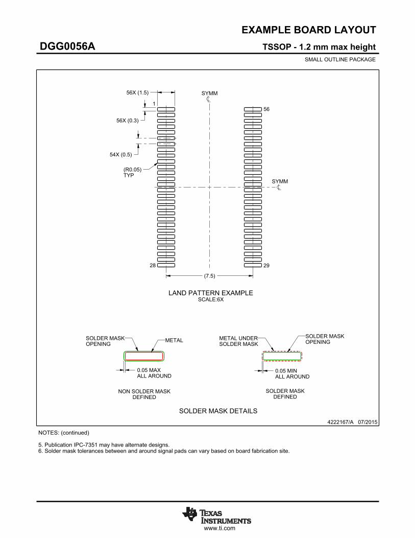
EXAMPLE BOARD LAYOUT
(7.5)
0.05 MAXALL AROUND
0.05 MINALL AROUND
56X (1.5)
56X (0.3)
54X (0.5)
(R )TYP
0.05
4222167/A 07/2015
TSSOP - 1.2 mm max heightDGG0056ASMALL OUTLINE PACKAGE
SYMM
SYMM
LAND PATTERN EXAMPLESCALE:6X
1
28 29
56
NOTES: (continued) 5. Publication IPC-7351 may have alternate designs. 6. Solder mask tolerances between and around signal pads can vary based on board fabrication site.
METALSOLDER MASKOPENING
NON SOLDER MASKDEFINED
SOLDER MASK DETAILS
SOLDER MASKOPENING
METAL UNDERSOLDER MASK
SOLDER MASKDEFINED
www.ti.com
EXAMPLE STENCIL DESIGN
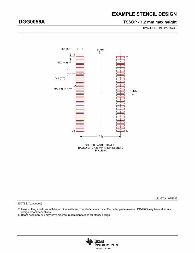
(7.5)
54X (0.5)
56X (0.3)
56X (1.5)
(R ) TYP0.05
4222167/A 07/2015
TSSOP - 1.2 mm max heightDGG0056ASMALL OUTLINE PACKAGE
NOTES: (continued) 7. Laser cutting apertures with trapezoidal walls and rounded corners may offer better paste release. IPC-7525 may have alternate design recommendations. 8. Board assembly site may have different recommendations for stencil design.
SYMM
SYMM
1
28 29
56
SOLDER PASTE EXAMPLEBASED ON 0.125 mm THICK STENCIL
SCALE:6X
www.ti.com
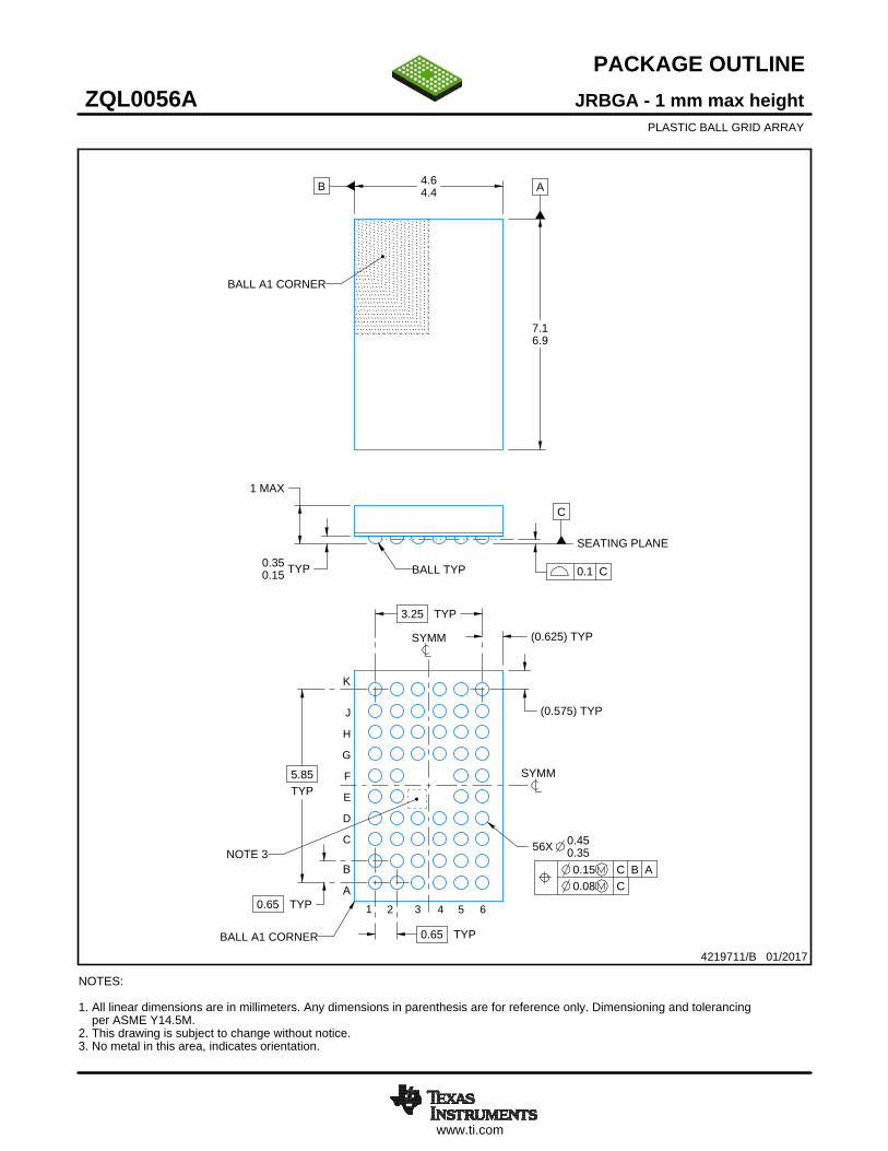
PACKAGE OUTLINE
C
1 MAX
TYP0.350.15
5.85TYP
3.25 TYP
0.65 TYP
0.65 TYP
56X 0.450.35
B 4.64.4 A
7.16.9
(0.625) TYP
(0.575) TYP
JRBGA - 1 mm max heightZQL0056APLASTIC BALL GRID ARRAY
4219711/B 01/2017
NOTES: 1. All linear dimensions are in millimeters. Any dimensions in parenthesis are for reference only. Dimensioning and tolerancing per ASME Y14.5M. 2. This drawing is subject to change without notice. 3. No metal in this area, indicates orientation.
BALL A1 CORNER
SEATING PLANE
BALL TYP 0.1 C
0.15 C B A0.08 C
SYMM
SYMM
BALL A1 CORNER
K
C
D
E
F
G
H
J
1 2 3 4 5 6
A
BNOTE 3
SCALE 2.100
www.ti.com
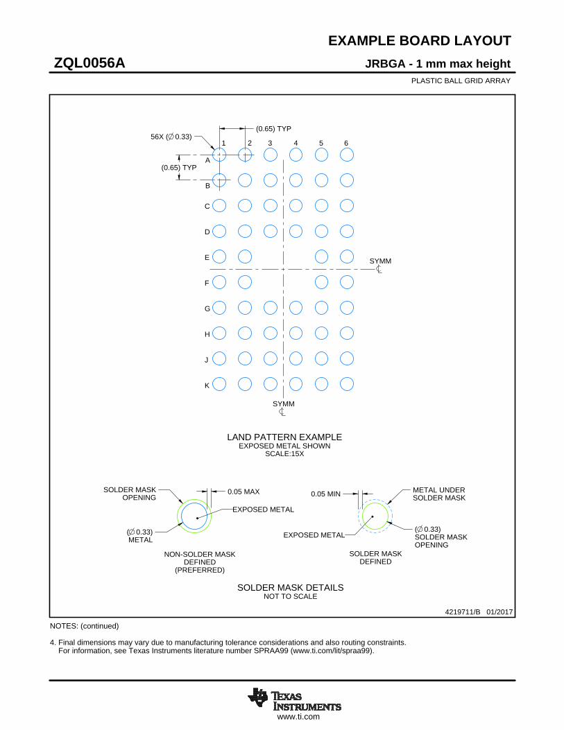
EXAMPLE BOARD LAYOUT
56X ( 0.33)(0.65) TYP
(0.65) TYP
( 0.33)METAL
0.05 MAXSOLDER MASKOPENING
METAL UNDERSOLDER MASK
( 0.33)SOLDER MASKOPENING
0.05 MIN
JRBGA - 1 mm max heightZQL0056APLASTIC BALL GRID ARRAY
4219711/B 01/2017
NOTES: (continued) 4. Final dimensions may vary due to manufacturing tolerance considerations and also routing constraints. For information, see Texas Instruments literature number SPRAA99 (www.ti.com/lit/spraa99).
SYMM
SYMM
LAND PATTERN EXAMPLEEXPOSED METAL SHOWN
SCALE:15X
1 2 3 4 5 6
A
C
D
E
F
G
H
J
K
B
NON-SOLDER MASKDEFINED
(PREFERRED)
SOLDER MASK DETAILSNOT TO SCALE
EXPOSED METAL
SOLDER MASKDEFINED
EXPOSED METAL
www.ti.com
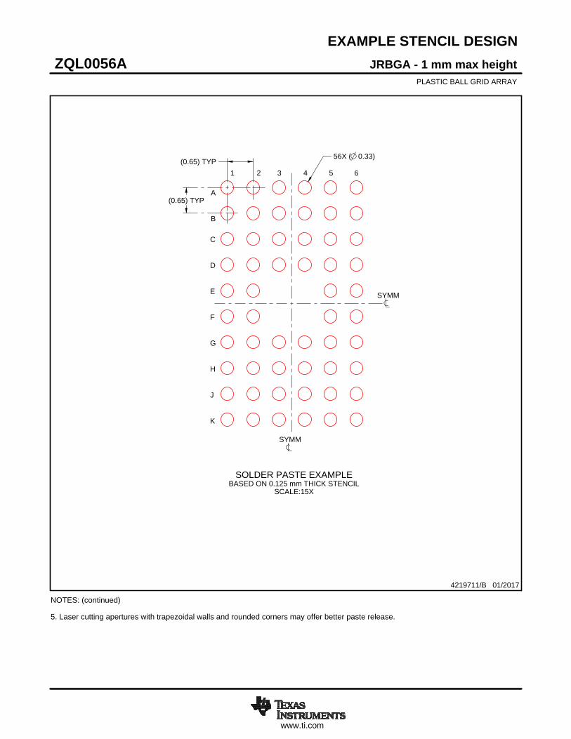
EXAMPLE STENCIL DESIGN
(0.65) TYP
(0.65) TYP56X ( 0.33)
JRBGA - 1 mm max heightZQL0056APLASTIC BALL GRID ARRAY
4219711/B 01/2017
NOTES: (continued) 5. Laser cutting apertures with trapezoidal walls and rounded corners may offer better paste release.
SOLDER PASTE EXAMPLEBASED ON 0.125 mm THICK STENCIL
SCALE:15X
SYMM
SYMM
1 2 3 4 5 6
A
C
D
E
F
G
H
J
K
B
IMPORTANT NOTICE
Texas Instruments Incorporated (TI) reserves the right to make corrections, enhancements, improvements and other changes to itssemiconductor products and services per JESD46, latest issue, and to discontinue any product or service per JESD48, latest issue. Buyersshould obtain the latest relevant information before placing orders and should verify that such information is current and complete.TI’s published terms of sale for semiconductor products (http://www.ti.com/sc/docs/stdterms.htm) apply to the sale of packaged integratedcircuit products that TI has qualified and released to market. Additional terms may apply to the use or sale of other types of TI products andservices.Reproduction of significant portions of TI information in TI data sheets is permissible only if reproduction is without alteration and isaccompanied by all associated warranties, conditions, limitations, and notices. TI is not responsible or liable for such reproduceddocumentation. Information of third parties may be subject to additional restrictions. Resale of TI products or services with statementsdifferent from or beyond the parameters stated by TI for that product or service voids all express and any implied warranties for theassociated TI product or service and is an unfair and deceptive business practice. TI is not responsible or liable for any such statements.Buyers and others who are developing systems that incorporate TI products (collectively, “Designers”) understand and agree that Designersremain responsible for using their independent analysis, evaluation and judgment in designing their applications and that Designers havefull and exclusive responsibility to assure the safety of Designers' applications and compliance of their applications (and of all TI productsused in or for Designers’ applications) with all applicable regulations, laws and other applicable requirements. Designer represents that, withrespect to their applications, Designer has all the necessary expertise to create and implement safeguards that (1) anticipate dangerousconsequences of failures, (2) monitor failures and their consequences, and (3) lessen the likelihood of failures that might cause harm andtake appropriate actions. Designer agrees that prior to using or distributing any applications that include TI products, Designer willthoroughly test such applications and the functionality of such TI products as used in such applications.TI’s provision of technical, application or other design advice, quality characterization, reliability data or other services or information,including, but not limited to, reference designs and materials relating to evaluation modules, (collectively, “TI Resources”) are intended toassist designers who are developing applications that incorporate TI products; by downloading, accessing or using TI Resources in anyway, Designer (individually or, if Designer is acting on behalf of a company, Designer’s company) agrees to use any particular TI Resourcesolely for this purpose and subject to the terms of this Notice.TI’s provision of TI Resources does not expand or otherwise alter TI’s applicable published warranties or warranty disclaimers for TIproducts, and no additional obligations or liabilities arise from TI providing such TI Resources. TI reserves the right to make corrections,enhancements, improvements and other changes to its TI Resources. TI has not conducted any testing other than that specificallydescribed in the published documentation for a particular TI Resource.Designer is authorized to use, copy and modify any individual TI Resource only in connection with the development of applications thatinclude the TI product(s) identified in such TI Resource. NO OTHER LICENSE, EXPRESS OR IMPLIED, BY ESTOPPEL OR OTHERWISETO ANY OTHER TI INTELLECTUAL PROPERTY RIGHT, AND NO LICENSE TO ANY TECHNOLOGY OR INTELLECTUAL PROPERTYRIGHT OF TI OR ANY THIRD PARTY IS GRANTED HEREIN, including but not limited to any patent right, copyright, mask work right, orother intellectual property right relating to any combination, machine, or process in which TI products or services are used. Informationregarding or referencing third-party products or services does not constitute a license to use such products or services, or a warranty orendorsement thereof. Use of TI Resources may require a license from a third party under the patents or other intellectual property of thethird party, or a license from TI under the patents or other intellectual property of TI.TI RESOURCES ARE PROVIDED “AS IS” AND WITH ALL FAULTS. TI DISCLAIMS ALL OTHER WARRANTIES ORREPRESENTATIONS, EXPRESS OR IMPLIED, REGARDING RESOURCES OR USE THEREOF, INCLUDING BUT NOT LIMITED TOACCURACY OR COMPLETENESS, TITLE, ANY EPIDEMIC FAILURE WARRANTY AND ANY IMPLIED WARRANTIES OFMERCHANTABILITY, FITNESS FOR A PARTICULAR PURPOSE, AND NON-INFRINGEMENT OF ANY THIRD PARTY INTELLECTUALPROPERTY RIGHTS. TI SHALL NOT BE LIABLE FOR AND SHALL NOT DEFEND OR INDEMNIFY DESIGNER AGAINST ANY CLAIM,INCLUDING BUT NOT LIMITED TO ANY INFRINGEMENT CLAIM THAT RELATES TO OR IS BASED ON ANY COMBINATION OFPRODUCTS EVEN IF DESCRIBED IN TI RESOURCES OR OTHERWISE. IN NO EVENT SHALL TI BE LIABLE FOR ANY ACTUAL,DIRECT, SPECIAL, COLLATERAL, INDIRECT, PUNITIVE, INCIDENTAL, CONSEQUENTIAL OR EXEMPLARY DAMAGES INCONNECTION WITH OR ARISING OUT OF TI RESOURCES OR USE THEREOF, AND REGARDLESS OF WHETHER TI HAS BEENADVISED OF THE POSSIBILITY OF SUCH DAMAGES.Unless TI has explicitly designated an individual product as meeting the requirements of a particular industry standard (e.g., ISO/TS 16949and ISO 26262), TI is not responsible for any failure to meet such industry standard requirements.Where TI specifically promotes products as facilitating functional safety or as compliant with industry functional safety standards, suchproducts are intended to help enable customers to design and create their own applications that meet applicable functional safety standardsand requirements. Using products in an application does not by itself establish any safety features in the application. Designers mustensure compliance with safety-related requirements and standards applicable to their applications. Designer may not use any TI products inlife-critical medical equipment unless authorized officers of the parties have executed a special contract specifically governing such use.Life-critical medical equipment is medical equipment where failure of such equipment would cause serious bodily injury or death (e.g., lifesupport, pacemakers, defibrillators, heart pumps, neurostimulators, and implantables). Such equipment includes, without limitation, allmedical devices identified by the U.S. Food and Drug Administration as Class III devices and equivalent classifications outside the U.S.TI may expressly designate certain products as completing a particular qualification (e.g., Q100, Military Grade, or Enhanced Product).Designers agree that it has the necessary expertise to select the product with the appropriate qualification designation for their applicationsand that proper product selection is at Designers’ own risk. Designers are solely responsible for compliance with all legal and regulatoryrequirements in connection with such selection.Designer will fully indemnify TI and its representatives against any damages, costs, losses, and/or liabilities arising out of Designer’s non-compliance with the terms and provisions of this Notice.
Mailing Address: Texas Instruments, Post Office Box 655303, Dallas, Texas 75265Copyright © 2018, Texas Instruments Incorporated


![MAX2986 Integrated Powerline Digital Transceiver · B13, D1, D11, D12, D13, E1, K4, M12 N.C. No Connection. Must be left unconnected (floating output). C3 GPIO[1] General-Purpose](https://img.pdfslide.net/doc/110x75/5f75225bee91b237682759ee/max2986-integrated-powerline-digital-transceiver-b13-d1-d11-d12-d13-e1-k4.jpg)