Embed Size (px)
Citation preview

1
2 181Y1
1OE
1A1
4 161Y21A2
6 141Y31A3
8 121Y41A4
19
11 92Y1
2OE
2A1
13 72Y22A2
15 52Y32A3
17 32Y42A4
Pin numbers shown are for the DB, DGV, DW, N, NS, PW, and RGY packages.
Product
Folder
Sample &Buy
Technical
Documents
Tools &
Software
Support &Community
An IMPORTANT NOTICE at the end of this data sheet addresses availability, warranty, changes, use in safety-critical applications,intellectual property matters and other important disclaimers. PRODUCTION DATA.
SN74LVC244ASCAS414AB –NOVEMBER 1992–REVISED NOVEMBER 2016
SN74LVC244A Octal Buffer or Driver With 3-State Outputs
1
1 Features1• Operates From 1.65 V to 3.6 V• Inputs Accept Voltages to 5.5 V• Specified From –40°C to +85°C and
–40°C to +125°C• Maximum tpd of 5.9 ns at 3.3 V• Typical VOLP (Output Ground Bounce)
< 0.8 V at VCC = 3.3 V, TA = 25°C• Typical VOHV (Output VOH Undershoot)
> 2 V at VCC = 3.3 V, TA = 25°C• Supports Mixed-Mode Signal Operation on
All Ports (5-V Input or Output Voltage With3.3-V VCC)
• Ioff Supports Live Insertion, Partial-Power-DownMode, and Back-Drive Protection
• Can Be Used as a Down Translator to TranslateInputs From a Maximum of 5.5 V Downto the VCC Level
• Available in Ultra Small Logic QFN Package (0.5mm Maximum Height)
• Latch-Up Performance Exceeds 250 mA PerJESD 17
• ESD Protection Exceeds JESD 22– 2000-V Human-Body Model– 1000-V Charged-Device Model
2 Applications• Servers• LED Displays• Network Switches• Telecom Infrastructure• Motor Drivers• I/O Expanders
3 DescriptionThese octal bus buffers are designed for 1.65-V to3.6-V VCC operation. The SN74LVC244A devicesare designed for asynchronous communicationbetween data buses.
Device InformationPART NUMBER PACKAGE BODY SIZE (NOM)
SN74LVC244AN PDIP (20) 25.40 mm × 6.35 mm
SN74LVC244ANS SO (20) 12.60 mm × 5.30 mm
SN74LVC244ADB SSOP (20) 7.50 mm × 5.30 mm
SN74LVC244ADGV TVSOP (20) 5.00 mm × 4.40 mm
SN74LVC244ADW SOIC (20) 12.80 mm × 7.50 mm
SN74LVC244ARGY VQFN (20) 4.50 mm × 3.50 mm
SN74LVC244AZQN BGA (20) 3.00 mm × 4.00 mm
SN74LVC244APW TSSOP (20) 6.50 mm × 4.40 mm
SN74LVC244ARWP X1QFN (20) 2.50 mm × 3.30 mm
(1) For all available packages, see the orderable addendum atthe end of the data sheet.
Logic Diagram (Positive Logic)

2
SN74LVC244ASCAS414AB –NOVEMBER 1992–REVISED NOVEMBER 2016 www.ti.com
Product Folder Links: SN74LVC244A
Submit Documentation Feedback Copyright © 1992–2016, Texas Instruments Incorporated
Table of Contents1 Features .................................................................. 12 Applications ........................................................... 13 Description ............................................................. 14 Revision History..................................................... 25 Pin Configuration and Functions ......................... 36 Specifications......................................................... 4
6.1 Absolute Maximum Ratings ...................................... 46.2 ESD Ratings.............................................................. 56.3 Recommended Operating Conditions....................... 56.4 Thermal Information .................................................. 56.5 Electrical Characteristics........................................... 66.6 Switching Characteristics .......................................... 66.7 Operating Characteristics.......................................... 76.8 Typical Characteristics .............................................. 7
7 Parameter Measurement Information .................. 88 Detailed Description .............................................. 9
8.1 Overview ................................................................... 9
8.2 Functional Block Diagram ......................................... 98.3 Feature Description................................................... 98.4 Device Functional Modes.......................................... 9
9 Application and Implementation ........................ 109.1 Application Information............................................ 109.2 Typical Application ................................................. 10
10 Power Supply Recommendations ..................... 1111 Layout................................................................... 11
11.1 Layout Guidelines ................................................. 1111.2 Layout Example .................................................... 11
12 Device and Documentation Support ................. 1212.1 Receiving Notification of Documentation Updates 1212.2 Community Resources.......................................... 1212.3 Trademarks ........................................................... 1212.4 Electrostatic Discharge Caution............................ 1212.5 Glossary ................................................................ 12
13 Mechanical, Packaging, and OrderableInformation ........................................................... 12
4 Revision HistoryNOTE: Page numbers for previous revisions may differ from page numbers in the current version.
Changes from Revision AA (June 2016) to Revision AB Page
• Changed A2 to A4 for 2OE in Pin Functions table ................................................................................................................. 4• Added ambient temperature, TA for BGA package and all other packages in Recommended Operating Conditions........... 5• Added Receiving Notification of Documentation Updates section ....................................................................................... 12
Changes from Revision Z (January 2015) to Revision AA Page
• Updated Device Information table to show all available packages ........................................................................................ 1• Added RWP Package ............................................................................................................................................................ 3• Deleted GQN package from Pin Functions table ................................................................................................................... 4• Added RWP thermal information to Thermal Information table and updated all thermal information for existing packages. 5• Updated all values for ZQN column in Thermal Information table ......................................................................................... 5• Added package type in Thermal Information table................................................................................................................. 5• Added RWP thermal information to Thermal Information table and updated all thermal information for existing packages. 6• Updated all values for ZQN column in Thermal Information table ......................................................................................... 6• Added package type in Thermal Information table................................................................................................................. 6
Changes from Revision Y (September 2010) to Revision Z Page
• Added Applications, Device Information table, Pin Functions table, ESD Ratings table, Thermal Information table,Typical Characteristics, Feature Description section, Device Functional Modes, Application and Implementationsection, Power Supply Recommendations section, Layout section, Device and Documentation Support section, andMechanical, Packaging, and Orderable Information section. ................................................................................................. 1
• Deleted Ordering Information table, see Mechanical, Packaging, and Orderable Information at the end of the datasheet.. 1• Updated Features. .................................................................................................................................................................. 1

Not to scale
Thermal
Pad
21A1
32Y4
41A2
52Y3
61A3
72Y2
81A4
92Y1
10
GN
D
11
2A
1
12 1Y4
13 2A2
14 1Y3
15 2A3
16 1Y2
17 2A4
18 1Y1
19 2OE
20
VC
C
11
OE
Not to scale
Thermal
Pad
11A1
22Y4
31A2
42Y3
51A3
62Y2
71
A4
82
Y1
9G
ND
10
2A
1
11 1Y4
12 2A2
13 1Y3
14 2A3
15 1Y2
16 2A41
71
Y1
18
2O
E
19
VC
C
20
1O
E
1 2 3 4
A
B
C
D
E
Not to scale
1A1 1OE VCC 2OE
1A2 2A4 2Y4 1Y1
1A3 2Y3 2A3 1Y2
1A4 2A2 2Y2 1Y3
GND 2Y1 2A1 1Y4 Not to scale
11OE 20 VCC
21A1 19 2OE
32Y4 18 1Y1
41A2 17 2A4
52Y3 16 1Y2
61A3 15 2A3
72Y2 14 1Y3
81A4 13 2A2
92Y1 12 1Y4
10GND 11 2A1
3
SN74LVC244Awww.ti.com SCAS414AB –NOVEMBER 1992–REVISED NOVEMBER 2016
Product Folder Links: SN74LVC244A
Submit Documentation FeedbackCopyright © 1992–2016, Texas Instruments Incorporated
5 Pin Configuration and Functions
ZQN Package20-Pin BGATop View
DB, DGV, DW, N, NS, and PW Packages20-Pin SSOP, TVSOP, SOIC, PDIP, SO, and TSSOP
Front View
RGY Package20-Pin VQFN
Top View
RWP Package20-Pin X1QFN
Top View
TI recommends to connect the exposed thermal pad to ground for best thermal performance. Must not be connectedto any other pin than ground.

4
SN74LVC244ASCAS414AB –NOVEMBER 1992–REVISED NOVEMBER 2016 www.ti.com
Product Folder Links: SN74LVC244A
Submit Documentation Feedback Copyright © 1992–2016, Texas Instruments Incorporated
Pin FunctionsPIN
TYPE DESCRIPTIONNAME
DB, DGV,DW, N, NS,
PW, andRGY
ZQN RWP
1A1 2 A1 1 I Port 1 A1 input
1A2 4 B1 3 I Port 1 A2 input
1A3 6 C1 5 I Port 1 A3 input
1A4 8 D1 7 I Port 1 A4 input
1OE 1 A2 20 I Output enable
1Y1 18 B4 17 O Port 1 Y1 output
1Y2 16 C4 15 O Port 1 Y2 output
1Y3 14 D4 13 O Port 1 Y3 output
1Y4 12 E4 11 O Port 1 Y4 output
2A1 11 E3 10 I Port 2 A1 input
2A2 13 D2 12 I Port 2 A2 input
2A3 15 C3 14 I Port 2 A3 input
2A4 17 B2 16 I Port 2 A4 input
2OE 19 A4 18 I Output enable
2Y1 9 E2 8 O Port 2 Y1 output
2Y2 7 D3 6 O Port 2 Y2 output
2Y3 5 C2 4 O Port 2 Y3 output
2Y4 3 B3 2 O Port 2 Y4 output
GND 10 E1 9 — Ground
VCC 20 A3 19 — Power pin
(1) Stresses beyond those listed under Absolute Maximum Ratings may cause permanent damage to the device. These are stress ratingsonly, and functional operation of the device at these or any other conditions beyond those indicated under Recommended OperatingConditions is not implied. Exposure to absolute-maximum-rated conditions for extended periods may affect device reliability.
(2) The input and output negative-voltage ratings may be exceeded if the input and output current ratings are observed.(3) The value of VCC is provided in the Recommended Operating Conditions table.(4) For the DW package: above 70°C the value of Ptot derates linearly with 8 mW/K.(5) For the DB, DGV, N, NS, and PW packages: above 60°C the value of Ptot derates linearly with 5.5 mW/K.
6 Specifications
6.1 Absolute Maximum Ratingsover operating free-air temperature range (unless otherwise noted) (1)
MIN MAX UNITVCC Supply voltage –0.5 6.5 VVI Input voltage (2) –0.5 6.5 VVO Voltage range applied to any output in the high-impedance or power-off state (2) –0.5 6.5 VVO Voltage range applied to any output in the high or low state (2) (3) –0.5 VCC + 0.5 VIIK Input clamp current VI < 0 –50 mAIOK Output clamp current VO < 0 –50 mAIO Continuous output current ±50 mA
Continuous current through VCC or GND ±100 mAPtot Power dissipation TA = –40°C to +125°C (4) (5) 500 mWTJ Junction temperature 150 °CTstg Storage temperature –65 150 °C

5
SN74LVC244Awww.ti.com SCAS414AB –NOVEMBER 1992–REVISED NOVEMBER 2016
Product Folder Links: SN74LVC244A
Submit Documentation FeedbackCopyright © 1992–2016, Texas Instruments Incorporated
(1) JEDEC document JEP155 states that 500-V HBM allows safe manufacturing with a standard ESD control process.(2) JEDEC document JEP157 states that 250-V CDM allows safe manufacturing with a standard ESD control process.
6.2 ESD RatingsVALUE UNIT
V(ESD) Electrostatic dischargeHuman-body model (HBM), per ANSI/ESDA/JEDEC JS-001 (1) ±2000
VCharged-device model (CDM), per JEDEC specification JESD22-C101 (2) ±1000
(1) All unused inputs of the device must be held at VCC or GND to ensure proper device operation. See Implications of Slow or FloatingCMOS Inputs, SCBA004.
6.3 Recommended Operating Conditionsover recommended operating free-air temperature range (unless otherwise noted) (1)
TA = 25°C –40 TO +85°C –40 TO +125°CUNIT
MIN MAX MIN MAX MIN MAX
VCC Supply voltageOperating 1.65 3.6 1.65 3.6 1.65 3.6
VData retention only 1.5 1.5 1.5
VIHHigh-levelinput voltage
VCC = 1.65 V to 1.95 V 0.65 × VCC 0.65 × VCC 0.65 × VCC
VVCC = 2.3 V to 2.7 V 1.7 1.7 1.7VCC = 2.7 V to 3.6 V 2 2 2
VILLow-levelinput voltage
VCC = 1.65 V to 1.95 V 0.35 × VCC 0.35 × VCC 0.35 × VCC
VVCC = 2.3 V to 2.7 V 0.7 0.7 0.7VCC = 2.7 V to 3.6 V 0.8 0.8 0.8
VI Input voltage 0 5.5 0 5.5 0 5.5 VVO Output voltage 0 VCC 0 VCC 0 VCC V
IOHHigh-leveloutput current
VCC = 1.65 V –4 –4 –4
mAVCC = 2.3 V –8 –8 –8VCC = 2.7 V –12 –12 –12VCC = 3 V –24 –24 –24
IOLLow-leveloutput current
VCC = 1.65 V 4 4 4
mAVCC = 2.3 V 8 8 8VCC = 2.7 V 12 12 12VCC = 3 V 24 24 24
TAAmbienttemperature
BGA package –40 85°C
All other packages –40 125
(1) For more information about traditional and new thermal metrics, see the Semiconductor and IC Package Thermal Metrics applicationreport.
(2) The package thermal impedance is calculated in accordance with JESD 51-7.(3) The package thermal impedance is calculated in accordance with JESD 51-5.
6.4 Thermal Information
THERMAL METRIC (1)
SN74LVC244A
UNITDB (2)
(SSOP)DGV (2)
(TVSOP)DW (2)
(SOIC)ZQN (2)
(BGA)N (2)
(PDIP)NS (2)
(SO)PW (2)
(TSSOP)RGY (3)
(VQFN)RWP (3)
(X1QFN)
20 PINS
RθJAJunction-to-ambientthermal resistance 108.1 128.7 90.9 198.7 61.6 90.1 114.7 50.3 79.9 °C/W
RθJC(top)Junction-to-case (top)thermal resistance 70.2 43.7 55.3 106.8 46.5 56.4 48.4 58.4 63.2 °C/W
RθJBJunction-to-boardthermal resistance 63.3 70.2 58.8 143.1 42.5 57.7 65.6 28.3 46.4 °C/W
ψJTJunction-to-topcharacterization parameter 30.6 3.1 29.1 24.1 34.6 28.4 6.8 4.9 2.6 °C/W
ψJBJunction-to-boardcharacterization parameter 62.9 69.5 58.3 119.6 42.4 57.2 65.1 28.4 46.3 °C/W

6
SN74LVC244ASCAS414AB –NOVEMBER 1992–REVISED NOVEMBER 2016 www.ti.com
Product Folder Links: SN74LVC244A
Submit Documentation Feedback Copyright © 1992–2016, Texas Instruments Incorporated
Thermal Information (continued)
THERMAL METRIC (1)
SN74LVC244A
UNITDB (2)
(SSOP)DGV (2)
(TVSOP)DW (2)
(SOIC)ZQN (2)
(BGA)N (2)
(PDIP)NS (2)
(SO)PW (2)
(TSSOP)RGY (3)
(VQFN)RWP (3)
(X1QFN)
20 PINS
RθJC(bot)Junction-to-case (bottom)thermal resistance — — — n/a — — — 22.7 27.3 °C/W
(1) This applies in the disabled state only.
6.5 Electrical Characteristicsover recommended operating free-air temperature range (unless otherwise noted)
PARAMETER TEST CONDITIONS VCCTA = 25°C –40 TO +85°C –40 TO +125°C
UNITMIN TYP MAX MIN MAX MIN MAX
VOH
IOH = –100 µA1.65 V
to3.6 V
VCC – 0.2 VCC – 0.2 VCC – 0.3
VIOH = –4 mA 1.65 V 1.29 1.2 1.05IOH = –8 mA 2.3 V 1.9 1.7 1.55
IOH = –12 mA2.7 V 2.2 2.2 2.053 V 2.4 2.4 2.25
IOH = –24 mA 3 V 2.3 2.2 2
VOL
IOL = 100 µA1.65 V
to3.6 V
0.1 0.2 0.3
VIOL = 4 mA 1.65 V 0.24 0.45 0.6IOL = 8 mA 2.3 V 0.3 0.7 0.75IOL = 12 mA 2.7 V 0.4 0.4 0.6IOL = 24 mA 3 V 0.55 0.55 0.8
II VI = 5.5 V or GND 3.6 V ±1 ±5 ±20 µAIoff VI or VO = 5.5 V 0 ±1 ±10 ±20 µAIOZ VO = 0 to 5.5 V 3.6 V ±1 ±10 ±20 µA
ICCVI = VCC or GND
IO = 0 3.6 V1 10 40
µA3.6 V ≤ VI ≤ 5.5 V (1) 1 10 40
ΔICCOne input at VCC – 0.6 V,Other inputs at VCC or GND
2.7 Vto
3.6 V500 500 5000 µA
Ci VI = VCC or GND 3.3 V 4 pFCo VO = VCC or GND 3.3 V 5.5 pF
6.6 Switching Characteristicsover recommended operating free-air temperature range (unless otherwise noted) (see Figure 3)
PARAMETER FROM(INPUT)
TO(OUTPUT) VCC
TA = 25°C –40 TO +85°C –40 TO +125°CUNIT
MIN TYP MAX MIN MAX MIN MAX
tpd A Y
1.5 V 1 7 14.4 1 14.9 1 16.4
ns
1.8 V ± 0.15 V 1 5.9 10.4 1 10.9 1 12.4
2.5 V ± 0.2 V 1 4.2 7.4 1 7.9 1 10
2.7 V 1 4.2 6.7 1 6.9 1 8.2
3.3 V ± 0.3 V 1.5 3.9 5.7 1.5 5.9 1.5 7.2

2
4
6
8
10
12
14
0 50 100 150 200 250 300
CL – Load Capacitance – pF
VCC = 3 V,
TA = 25°C
One Output Switching
Four Outputs Switching
Eight Outputs Switching
t–
Pro
pag
ati
on
Dela
yT
ime
–n
sp
d
2
4
6
8
10
0 50 100 150 200 250 300
CL – Load Capacitance – pF
t–
Pro
pa
ga
tio
nD
ela
yT
ime
–n
sp
d
VCC = 3 V,
TA = 25°C
One Output Switching
Four Outputs Switching
Eight Outputs Switching
7
SN74LVC244Awww.ti.com SCAS414AB –NOVEMBER 1992–REVISED NOVEMBER 2016
Product Folder Links: SN74LVC244A
Submit Documentation FeedbackCopyright © 1992–2016, Texas Instruments Incorporated
Switching Characteristics (continued)over recommended operating free-air temperature range (unless otherwise noted) (see Figure 3)
PARAMETER FROM(INPUT)
TO(OUTPUT) VCC
TA = 25°C –40 TO +85°C –40 TO +125°CUNIT
MIN TYP MAX MIN MAX MIN MAX
ten OE Y
1.5 V 1 8.3 17.8 1 18.3 1 19.8
ns
1.8 V ± 0.15 V 1 6.4 12.1 1 12.6 1 14.1
2.5 V ± 0.2 V 1 4.6 9.1 1 9.6 1 11.7
2.7 V 1 5 8.4 1 8.6 1 10.3
3.3 V ± 0.3 V 1.5 4.5 7.4 1.5 7.6 1.5 9.4
tdis OE Y
1.5 V 1 7.2 15.6 1 16.1 1 17.6
ns
1.8 V ± 0.15 V 1 5.8 11.6 1 12.1 1 13.6
2.5 V ± 0.2 V 1 3.7 7.3 1 7.8 1 9.9
2.7 V 1 3.8 6.6 1 6.8 1 8.6
3.3 V ± 0.3 V 1.5 3.8 6.3 1.5 6.5 1.5 8
tsk(o) 3.3 V ± 0.3 V 1 1.5 ns
6.7 Operating CharacteristicsTA = 25°C
PARAMETER TEST CONDITIONS VCC TYP UNIT
Cpd Power dissipation capacitance per buffer/driver
Outputs enabled f = 10 MHz1.8 V 43
pF
2.5 V 433.3 V 44
Outputs disabled f = 10 MHz1.8 V 12.5 V 13.3 V 2
6.8 Typical Characteristics
Figure 1. Propagation Delay (Low to High Transition)vs Load Capacitance
Figure 2. Propagation Delay (High to Low Transition)vs Load Capacitance

VM
thtsu
From Output
Under Test
CL
(see Note A)
LOAD CIRCUIT
S1
VLOAD
Open
GND
R
R
L
L
Data Input
Timing Input
VI
0 V
VI
0 V0 V
t
Input
w
VOLTAGE WAVEFORMS
SETUP AND HOLD TIMES
VOLTAGE WAVEFORMS
PROPAGATION DELAY TIMES
INVERTING AND NONINVERTING OUTPUTS
VOLTAGE WAVEFORMS
PULSE DURATION
tPLH
tPHL
tPHL
tPLH
VOH
VOH
VOL
VOL
VI
0 VInput
Output
Waveform 1
S1 at VLOAD
(see Note B)
Output
Waveform 2
S1 at GND
(see Note B)
VOL
VOH
tPZL
tPZH
tPLZ
tPHZ
VLOAD/2
0 V
VOL + V∆
VOH − V∆
≈0 V
VI
VOLTAGE WAVEFORMS
ENABLE AND DISABLE TIMES
LOW- AND HIGH-LEVEL ENABLING
Output
Output
tPLH/tPHL
tPLZ/tPZL
tPHZ/tPZH
Open
VLOAD
GND
TEST S1
NOTES: A. CL includes probe and jig capacitance.
B. Waveform 1 is for an output with internal conditions such that the output is low, except when disabled by the output control.
Waveform 2 is for an output with internal conditions such that the output is high, except when disabled by the output control.
C. All input pulses are supplied by generators having the following characteristics: PRR≤ 10 MHz, ZO = 50 Ω.
D. The outputs are measured one at a time, with one transition per measurement.
E. tPLZ and tPHZ are the same as tdis.
F. tPZL and tPZH are the same as ten.
G. tPLH and tPHL are the same as tpd.
H. All parameters and waveforms are not applicable to all devices.
Output
Control
V V
V V
V V
V
V V
V
V
V
V
M M
M M
M M
M
M M
M
M
M
I
VM
VM
1.5 V
1.8 V ± 0.15 V
2.5 V ± 0.2 V
2.7 V
3.3 V ± 0.3 V
2 kΩ
1 kΩ
500 Ω
500 Ω
500 Ω
VCC RL
2 × VCC
2 × VCC
2 × VCC
6 V
6 V
VLOAD CL
15 pF
30 pF
30 pF
50 pF
50 pF
0.1 V
0.15 V
0.15 V
0.3 V
0.3 V
V
V
∆
CC
VCC
VCC
2.7 V
2.7 V
V
V
I
CC/2
VCC/2
VCC/2
1.5 V
1.5 V
VMt /tr f
≤2 ns
≤2 ns
≤2 ns
≤2.5 ns
≤2.5 ns
INPUTS
8
SN74LVC244ASCAS414AB –NOVEMBER 1992–REVISED NOVEMBER 2016 www.ti.com
Product Folder Links: SN74LVC244A
Submit Documentation Feedback Copyright © 1992–2016, Texas Instruments Incorporated
7 Parameter Measurement Information
Figure 3. Load Circuit and Voltage Waveforms

1
2 181Y1
1OE
1A1
4 161Y21A2
6 141Y31A3
8 121Y41A4
19
11 92Y1
2OE
2A1
13 72Y22A2
15 52Y32A3
17 32Y42A4
Pin numbers shown are for the DB, DGV, DW, N, NS, PW, and RGY packages.
9
SN74LVC244Awww.ti.com SCAS414AB –NOVEMBER 1992–REVISED NOVEMBER 2016
Product Folder Links: SN74LVC244A
Submit Documentation FeedbackCopyright © 1992–2016, Texas Instruments Incorporated
8 Detailed Description
8.1 OverviewThe SN74LVC244A device is organized as two 4-bit buffers/line drivers with separate output-enable (OE) inputs.The device passes data from the A inputs to the Y outputs when OE is low. The outputs are in the high-impedance state when OE is high. OE should be tied to VCC through a pullup resistor to ensure the high-impedance state during power up or power down; the minimum value of the resistor is determined by the current-sinking capability of the driver.
8.2 Functional Block Diagram
Figure 4. Logic Diagram (Positive Logic)
8.3 Feature Description• Allows down voltage translation
– 5 V to 3.3 V– 5 V or 3.3 V to 1.8 V
• Inputs accept voltage levels up to 5.5 V• It is available in ultra small logic 20 pin QFN package at 0.5 mm max height with 0.4 mm pitch.
8.4 Device Functional ModesTable 1 lists the functional modes of the SN74LVC244A.
Table 1. Function TableINPUTS OUTPUT
YOE AL H HL L LH X Hi-Z

uC or
System
Logic
A1
A4
VCC
Y4
Y1
1OE
uC
System Logic
LEDs
Regulated 3 V
GND
SN74LVC244A
10
SN74LVC244ASCAS414AB –NOVEMBER 1992–REVISED NOVEMBER 2016 www.ti.com
Product Folder Links: SN74LVC244A
Submit Documentation Feedback Copyright © 1992–2016, Texas Instruments Incorporated
9 Application and Implementation
NOTEInformation in the following applications sections is not part of the TI componentspecification, and TI does not warrant its accuracy or completeness. TI’s customers areresponsible for determining suitability of components for their purposes. Customers shouldvalidate and test their design implementation to confirm system functionality.
9.1 Application InformationSN74LVC244A is a high drive CMOS device that can be used for a multitude of bus interface type applicationswhere output drive or PCB trace length is a concern. The inputs can accept voltages to 5.5 V at any valid VCCmaking it ideal for down translation.
9.2 Typical Application
Figure 5. Application Schematic
9.2.1 Design RequirementsThis device uses CMOS technology and has balanced output drive. Avoid bus contention because it can drivecurrents in excess of maximum limits. The high drive will also create fast edges into light loads, so considerrouting and load conditions to prevent ringing.
9.2.2 Detailed Design Procedure1. Recommended Input Conditions:
– For rise time and fall time specification, see (Δt/ΔV) in the Recommended Operating Conditions table.– For specified high and low levels, see (VIH and VIL) in the Recommended Operating Conditions table.– Inputs are overvoltage tolerant allowing them to go as high as (VI max) in the Recommended Operating
Conditions table at any valid VCC.2. Recommended maximum Output Conditions:
– Load currents should not exceed (IO max) per output and should not exceed (Continuous current throughVCC or GND) total current for the part. These limits are located in the Absolute Maximum Ratings table.
– Outputs should not be pulled above VCC.

VCC
Unused Input
Input
Output Output
Input
Unused Input
–100
–80
–60
–40
–20
0
20
40
60
–1 –0.5 0.0 0.5 1.0 1.5 2.0 2.5 3.0 3.5 4.0
TA = 25°C, VCC = 3 V,
VIH = 3 V, VIL = 0 V,
All Outputs Switching
VOH – VI O
H–
mA
VOL – V
–20
0
20
40
60
80
100
–0.2 0.0 0.2 0.4 0.6 0.8 1.0 1.2 1.4 1.6
TA = 25°C, VCC = 3 V,
VIH = 3 V, VIL = 0 V,
All Outputs Switching
I OL
–m
A
11
SN74LVC244Awww.ti.com SCAS414AB –NOVEMBER 1992–REVISED NOVEMBER 2016
Product Folder Links: SN74LVC244A
Submit Documentation FeedbackCopyright © 1992–2016, Texas Instruments Incorporated
Typical Application (continued)9.2.3 Application Curves
Figure 6. Output Drive Current (IOL)vs LOW-level Output Voltage (VOL)
Figure 7. Output Drive Current (IOH)vs HIGH-level Output Voltage (VOH)
10 Power Supply RecommendationsThe power supply may be any voltage between the MIN and MAX supply voltage rating located in theRecommended Operating Conditions table.
Each VCC terminal should have a good bypass capacitor to prevent power disturbance. A 0.1 μF capacitor isrecommended for devices with a single supply. If there are multiple VCC terminals, then 0.01 μF or 0.022 μFcapacitors are recommended for each power terminal. It is permissible to parallel multiple bypass capacitors toreject different frequencies of noise. Multiple bypass capacitors may be paralleled to reject different frequenciesof noise. The bypass capacitor should be installed as close to the power terminal as possible for the best results.
11 Layout
11.1 Layout GuidelinesInputs should not float when using multiple bit logic devices. In many cases, functions or parts of functions ofdigital logic devices are unused. Some examples include situations when only two inputs of a triple-input ANDgate are used, or when only 3 of the 4-buffer gates are used. Such input pins should not be left unconnectedbecause the undefined voltages at the outside connections result in undefined operational states.
Specified in Figure 8 are rules that must be observed under all circumstances. All unused inputs of digital logicdevices must be connected to a high or low bias to prevent them from floating. The logic level that should beapplied to any particular unused input depends on the function of the device. Generally, they will be tied to GNDor VCC, whichever makes more sense or is more convenient.
11.2 Layout Example
Figure 8. Layout Diagram

12
SN74LVC244ASCAS414AB –NOVEMBER 1992–REVISED NOVEMBER 2016 www.ti.com
Product Folder Links: SN74LVC244A
Submit Documentation Feedback Copyright © 1992–2016, Texas Instruments Incorporated
12 Device and Documentation Support
12.1 Receiving Notification of Documentation UpdatesTo receive notification of documentation updates, navigate to the device product folder on ti.com. In the upperright corner, click on Alert me to register and receive a weekly digest of any product information that haschanged. For change details, review the revision history included in any revised document.
12.2 Community ResourcesThe following links connect to TI community resources. Linked contents are provided "AS IS" by the respectivecontributors. They do not constitute TI specifications and do not necessarily reflect TI's views; see TI's Terms ofUse.
TI E2E™ Online Community TI's Engineer-to-Engineer (E2E) Community. Created to foster collaborationamong engineers. At e2e.ti.com, you can ask questions, share knowledge, explore ideas and helpsolve problems with fellow engineers.
Design Support TI's Design Support Quickly find helpful E2E forums along with design support tools andcontact information for technical support.
12.3 TrademarksE2E is a trademark of Texas Instruments.All other trademarks are the property of their respective owners.
12.4 Electrostatic Discharge CautionThese devices have limited built-in ESD protection. The leads should be shorted together or the device placed in conductive foamduring storage or handling to prevent electrostatic damage to the MOS gates.
12.5 GlossarySLYZ022 — TI Glossary.
This glossary lists and explains terms, acronyms, and definitions.
13 Mechanical, Packaging, and Orderable InformationThe following pages include mechanical packaging and orderable information. This information is the mostcurrent data available for the designated devices. This data is subject to change without notice and revision ofthis document. For browser based versions of this data sheet, refer to the left hand navigation.

PACKAGE OPTION ADDENDUM
www.ti.com 17-Mar-2017
Addendum-Page 1
PACKAGING INFORMATION
Orderable Device Status(1)
Package Type PackageDrawing
Pins PackageQty
Eco Plan(2)
Lead/Ball Finish(6)
MSL Peak Temp(3)
Op Temp (°C) Device Marking(4/5)
Samples
SN74LVC244ADBR ACTIVE SSOP DB 20 2000 Green (RoHS& no Sb/Br)
CU NIPDAU Level-1-260C-UNLIM -40 to 125 LC244A
SN74LVC244ADBRE4 ACTIVE SSOP DB 20 2000 Green (RoHS& no Sb/Br)
CU NIPDAU Level-1-260C-UNLIM -40 to 125 LC244A
SN74LVC244ADBRG4 ACTIVE SSOP DB 20 2000 Green (RoHS& no Sb/Br)
CU NIPDAU Level-1-260C-UNLIM -40 to 125 LC244A
SN74LVC244ADGVR ACTIVE TVSOP DGV 20 2000 Green (RoHS& no Sb/Br)
CU NIPDAU Level-1-260C-UNLIM -40 to 125 LC244A
SN74LVC244ADGVRE4 ACTIVE TVSOP DGV 20 2000 Green (RoHS& no Sb/Br)
CU NIPDAU Level-1-260C-UNLIM -40 to 125 LC244A
SN74LVC244ADGVRG4 ACTIVE TVSOP DGV 20 2000 Green (RoHS& no Sb/Br)
CU NIPDAU Level-1-260C-UNLIM -40 to 125 LC244A
SN74LVC244ADW ACTIVE SOIC DW 20 25 Green (RoHS& no Sb/Br)
CU NIPDAU Level-1-260C-UNLIM -40 to 125 LVC244A
SN74LVC244ADWE4 ACTIVE SOIC DW 20 25 Green (RoHS& no Sb/Br)
CU NIPDAU Level-1-260C-UNLIM -40 to 125 LVC244A
SN74LVC244ADWG4 ACTIVE SOIC DW 20 25 Green (RoHS& no Sb/Br)
CU NIPDAU Level-1-260C-UNLIM -40 to 125 LVC244A
SN74LVC244ADWR ACTIVE SOIC DW 20 2000 Green (RoHS& no Sb/Br)
CU NIPDAU | CU SN Level-1-260C-UNLIM -40 to 125 LVC244A
SN74LVC244ADWRE4 ACTIVE SOIC DW 20 2000 Green (RoHS& no Sb/Br)
CU NIPDAU Level-1-260C-UNLIM -40 to 125 LVC244A
SN74LVC244ADWRG4 ACTIVE SOIC DW 20 2000 Green (RoHS& no Sb/Br)
CU NIPDAU Level-1-260C-UNLIM -40 to 125 LVC244A
SN74LVC244AN ACTIVE PDIP N 20 20 Pb-Free(RoHS)
CU NIPDAU N / A for Pkg Type -40 to 125 SN74LVC244AN
SN74LVC244ANE4 ACTIVE PDIP N 20 20 Pb-Free(RoHS)
CU NIPDAU N / A for Pkg Type -40 to 125 SN74LVC244AN
SN74LVC244ANSR ACTIVE SO NS 20 2000 Green (RoHS& no Sb/Br)
CU NIPDAU Level-1-260C-UNLIM -40 to 125 LVC244A
SN74LVC244ANSRE4 ACTIVE SO NS 20 2000 Green (RoHS& no Sb/Br)
CU NIPDAU Level-1-260C-UNLIM -40 to 125 LVC244A
SN74LVC244APW ACTIVE TSSOP PW 20 70 Green (RoHS& no Sb/Br)
CU NIPDAU Level-1-260C-UNLIM -40 to 125 LC244A

PACKAGE OPTION ADDENDUM
www.ti.com 17-Mar-2017
Addendum-Page 2
Orderable Device Status(1)
Package Type PackageDrawing
Pins PackageQty
Eco Plan(2)
Lead/Ball Finish(6)
MSL Peak Temp(3)
Op Temp (°C) Device Marking(4/5)
Samples
SN74LVC244APWE4 ACTIVE TSSOP PW 20 70 Green (RoHS& no Sb/Br)
CU NIPDAU Level-1-260C-UNLIM -40 to 125 LC244A
SN74LVC244APWG4 ACTIVE TSSOP PW 20 70 Green (RoHS& no Sb/Br)
CU NIPDAU Level-1-260C-UNLIM -40 to 125 LC244A
SN74LVC244APWR ACTIVE TSSOP PW 20 2000 Green (RoHS& no Sb/Br)
CU NIPDAU | CU SN Level-1-260C-UNLIM -40 to 125 LC244A
SN74LVC244APWRE4 ACTIVE TSSOP PW 20 2000 Green (RoHS& no Sb/Br)
CU NIPDAU Level-1-260C-UNLIM -40 to 125 LC244A
SN74LVC244APWRG3 ACTIVE TSSOP PW 20 2000 Green (RoHS& no Sb/Br)
CU SN Level-1-260C-UNLIM -40 to 125 LC244A
SN74LVC244APWRG4 ACTIVE TSSOP PW 20 2000 Green (RoHS& no Sb/Br)
CU NIPDAU Level-1-260C-UNLIM -40 to 125 LC244A
SN74LVC244APWT ACTIVE TSSOP PW 20 250 Green (RoHS& no Sb/Br)
CU NIPDAU Level-1-260C-UNLIM -40 to 125 LC244A
SN74LVC244APWTE4 ACTIVE TSSOP PW 20 250 Green (RoHS& no Sb/Br)
CU NIPDAU Level-1-260C-UNLIM -40 to 125 LC244A
SN74LVC244APWTG4 ACTIVE TSSOP PW 20 250 Green (RoHS& no Sb/Br)
CU NIPDAU Level-1-260C-UNLIM -40 to 125 LC244A
SN74LVC244ARGYR ACTIVE VQFN RGY 20 3000 Green (RoHS& no Sb/Br)
CU NIPDAU Level-2-260C-1 YEAR -40 to 125 LC244A
SN74LVC244ARGYRG4 ACTIVE VQFN RGY 20 3000 Green (RoHS& no Sb/Br)
CU NIPDAU Level-2-260C-1 YEAR -40 to 125 LC244A
SN74LVC244ARWPR ACTIVE X1QFN RWP 20 2000 Green (RoHS& no Sb/Br)
CU NIPDAU Level-1-260C-UNLIM -40 to 125 LC244A
SN74LVC244AZQNR ACTIVE BGAMICROSTAR
JUNIOR
ZQN 20 1000 Green (RoHS& no Sb/Br)
SNAGCU Level-1-260C-UNLIM -40 to 85 LC244A
(1) The marketing status values are defined as follows:ACTIVE: Product device recommended for new designs.LIFEBUY: TI has announced that the device will be discontinued, and a lifetime-buy period is in effect.NRND: Not recommended for new designs. Device is in production to support existing customers, but TI does not recommend using this part in a new design.PREVIEW: Device has been announced but is not in production. Samples may or may not be available.OBSOLETE: TI has discontinued the production of the device.
(2) Eco Plan - The planned eco-friendly classification: Pb-Free (RoHS), Pb-Free (RoHS Exempt), or Green (RoHS & no Sb/Br) - please check http://www.ti.com/productcontent for the latest availabilityinformation and additional product content details.

PACKAGE OPTION ADDENDUM
www.ti.com 17-Mar-2017
Addendum-Page 3
TBD: The Pb-Free/Green conversion plan has not been defined.Pb-Free (RoHS): TI's terms "Lead-Free" or "Pb-Free" mean semiconductor products that are compatible with the current RoHS requirements for all 6 substances, including the requirement thatlead not exceed 0.1% by weight in homogeneous materials. Where designed to be soldered at high temperatures, TI Pb-Free products are suitable for use in specified lead-free processes.Pb-Free (RoHS Exempt): This component has a RoHS exemption for either 1) lead-based flip-chip solder bumps used between the die and package, or 2) lead-based die adhesive used betweenthe die and leadframe. The component is otherwise considered Pb-Free (RoHS compatible) as defined above.Green (RoHS & no Sb/Br): TI defines "Green" to mean Pb-Free (RoHS compatible), and free of Bromine (Br) and Antimony (Sb) based flame retardants (Br or Sb do not exceed 0.1% by weightin homogeneous material)
(3) MSL, Peak Temp. - The Moisture Sensitivity Level rating according to the JEDEC industry standard classifications, and peak solder temperature.
(4) There may be additional marking, which relates to the logo, the lot trace code information, or the environmental category on the device.
(5) Multiple Device Markings will be inside parentheses. Only one Device Marking contained in parentheses and separated by a "~" will appear on a device. If a line is indented then it is a continuationof the previous line and the two combined represent the entire Device Marking for that device.
(6) Lead/Ball Finish - Orderable Devices may have multiple material finish options. Finish options are separated by a vertical ruled line. Lead/Ball Finish values may wrap to two lines if the finishvalue exceeds the maximum column width.
Important Information and Disclaimer:The information provided on this page represents TI's knowledge and belief as of the date that it is provided. TI bases its knowledge and belief on informationprovided by third parties, and makes no representation or warranty as to the accuracy of such information. Efforts are underway to better integrate information from third parties. TI has taken andcontinues to take reasonable steps to provide representative and accurate information but may not have conducted destructive testing or chemical analysis on incoming materials and chemicals.TI and TI suppliers consider certain information to be proprietary, and thus CAS numbers and other limited information may not be available for release.
In no event shall TI's liability arising out of such information exceed the total purchase price of the TI part(s) at issue in this document sold by TI to Customer on an annual basis.
OTHER QUALIFIED VERSIONS OF SN74LVC244A :
• Automotive: SN74LVC244A-Q1
NOTE: Qualified Version Definitions:
• Automotive - Q100 devices qualified for high-reliability automotive applications targeting zero defects
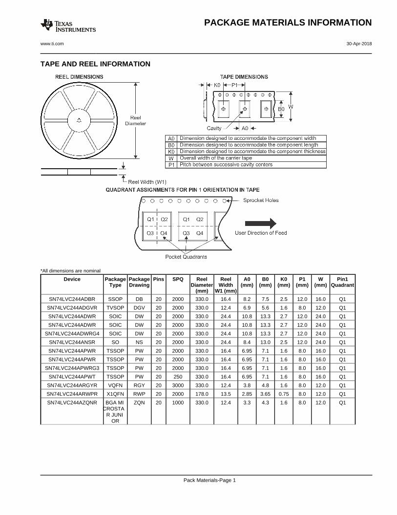
TAPE AND REEL INFORMATION
*All dimensions are nominal
Device PackageType
PackageDrawing
Pins SPQ ReelDiameter
(mm)
ReelWidth
W1 (mm)
A0(mm)
B0(mm)
K0(mm)
P1(mm)
W(mm)
Pin1Quadrant
SN74LVC244ADBR SSOP DB 20 2000 330.0 16.4 8.2 7.5 2.5 12.0 16.0 Q1
SN74LVC244ADGVR TVSOP DGV 20 2000 330.0 12.4 6.9 5.6 1.6 8.0 12.0 Q1
SN74LVC244ADWR SOIC DW 20 2000 330.0 24.4 10.8 13.3 2.7 12.0 24.0 Q1
SN74LVC244ADWR SOIC DW 20 2000 330.0 24.4 10.8 13.3 2.7 12.0 24.0 Q1
SN74LVC244ADWRG4 SOIC DW 20 2000 330.0 24.4 10.8 13.3 2.7 12.0 24.0 Q1
SN74LVC244ANSR SO NS 20 2000 330.0 24.4 8.4 13.0 2.5 12.0 24.0 Q1
SN74LVC244APWR TSSOP PW 20 2000 330.0 16.4 6.95 7.1 1.6 8.0 16.0 Q1
SN74LVC244APWR TSSOP PW 20 2000 330.0 16.4 6.95 7.1 1.6 8.0 16.0 Q1
SN74LVC244APWRG3 TSSOP PW 20 2000 330.0 16.4 6.95 7.1 1.6 8.0 16.0 Q1
SN74LVC244APWT TSSOP PW 20 250 330.0 16.4 6.95 7.1 1.6 8.0 16.0 Q1
SN74LVC244ARGYR VQFN RGY 20 3000 330.0 12.4 3.8 4.8 1.6 8.0 12.0 Q1
SN74LVC244ARWPR X1QFN RWP 20 2000 178.0 13.5 2.85 3.65 0.75 8.0 12.0 Q1
SN74LVC244AZQNR BGA MI CROSTA
R JUNI OR
ZQN 20 1000 330.0 12.4 3.3 4.3 1.6 8.0 12.0 Q1
PACKAGE MATERIALS INFORMATION
www.ti.com 30-Apr-2018
Pack Materials-Page 1

*All dimensions are nominal
Device Package Type Package Drawing Pins SPQ Length (mm) Width (mm) Height (mm)
SN74LVC244ADBR SSOP DB 20 2000 367.0 367.0 38.0
SN74LVC244ADGVR TVSOP DGV 20 2000 367.0 367.0 35.0
SN74LVC244ADWR SOIC DW 20 2000 367.0 367.0 45.0
SN74LVC244ADWR SOIC DW 20 2000 364.0 361.0 36.0
SN74LVC244ADWRG4 SOIC DW 20 2000 367.0 367.0 45.0
SN74LVC244ANSR SO NS 20 2000 367.0 367.0 45.0
SN74LVC244APWR TSSOP PW 20 2000 364.0 364.0 27.0
SN74LVC244APWR TSSOP PW 20 2000 367.0 367.0 38.0
SN74LVC244APWRG3 TSSOP PW 20 2000 364.0 364.0 27.0
SN74LVC244APWT TSSOP PW 20 250 367.0 367.0 38.0
SN74LVC244ARGYR VQFN RGY 20 3000 355.0 350.0 50.0
SN74LVC244ARWPR X1QFN RWP 20 2000 189.0 185.0 36.0
SN74LVC244AZQNR BGA MICROSTARJUNIOR
ZQN 20 1000 336.6 336.6 28.6
PACKAGE MATERIALS INFORMATION
www.ti.com 30-Apr-2018
Pack Materials-Page 2


MECHANICAL DATA
MSSO002E – JANUARY 1995 – REVISED DECEMBER 2001
POST OFFICE BOX 655303 • DALLAS, TEXAS 75265
DB (R-PDSO-G**) PLASTIC SMALL-OUTLINE
4040065 /E 12/01
28 PINS SHOWN
Gage Plane
8,207,40
0,550,95
0,25
38
12,90
12,30
28
10,50
24
8,50
Seating Plane
9,907,90
30
10,50
9,90
0,38
5,605,00
15
0,22
14
A
28
1
2016
6,506,50
14
0,05 MIN
5,905,90
DIM
A MAX
A MIN
PINS **
2,00 MAX
6,90
7,50
0,65 M0,15
0°–8°
0,10
0,090,25
NOTES: A. All linear dimensions are in millimeters.B. This drawing is subject to change without notice.C. Body dimensions do not include mold flash or protrusion not to exceed 0,15.D. Falls within JEDEC MO-150

www.ti.com
PACKAGE OUTLINE
C
20X 0.250.15
1.14±0.05
20X 0.50.3
0.5 MAX
(0.15) TYP
0.050.00
16X 0.4
2X2
2X 1.2
1.9±0.05
A 2.62.4
B
3.43.2
4X (0.36)
(0.1) TYP
X1QFN - 0.5 mm max heightRWP0020APLASTIC QUAD FLATPACK - NO LEAD
4221912/A 03/2015
PIN 1 INDEX AREA
0.08
SEATING PLANE
1
6 11
16
7 10
20 17(OPTIONAL)
PIN 1 ID 0.1 C A B0.05
EXPOSEDTHERMAL PAD
NOTES: 1. All linear dimensions are in millimeters. Any dimensions in parenthesis are for reference only. Dimensioning and tolerancing per ASME Y14.5M. 2. This drawing is subject to change without notice. 3. The package thermal pad must be soldered to the printed circuit board for thermal and mechanical performance.
SCALE 4.200

www.ti.com
EXAMPLE BOARD LAYOUT
0.05 MINALL AROUND
0.05 MAXALL AROUND
20X (0.2)
20X (0.6)
( ) TYPVIA
0.2
16X (0.4)
(3.1)
(2.3)
(0.7)
(1.14)
(R )TYP
0.05
(1.9)
X1QFN - 0.5 mm max heightRWP0020APLASTIC QUAD FLATPACK - NO LEAD
4221912/A 03/2015
SYMM
1
6
7 10
11
16
1720
SYMM
LAND PATTERN EXAMPLESCALE:20X
NOTES: (continued) 4. This package is designed to be soldered to a thermal pad on the board. For more information, see Texas Instruments literature number SLUA271 (www.ti.com/lit/slua271).
SOLDER MASKOPENING
METAL UNDERSOLDER MASK
SOLDER MASKDEFINED
METAL
SOLDER MASKOPENING
SOLDER MASK DETAILS
NON SOLDER MASKDEFINED
(PREFERRED)

www.ti.com
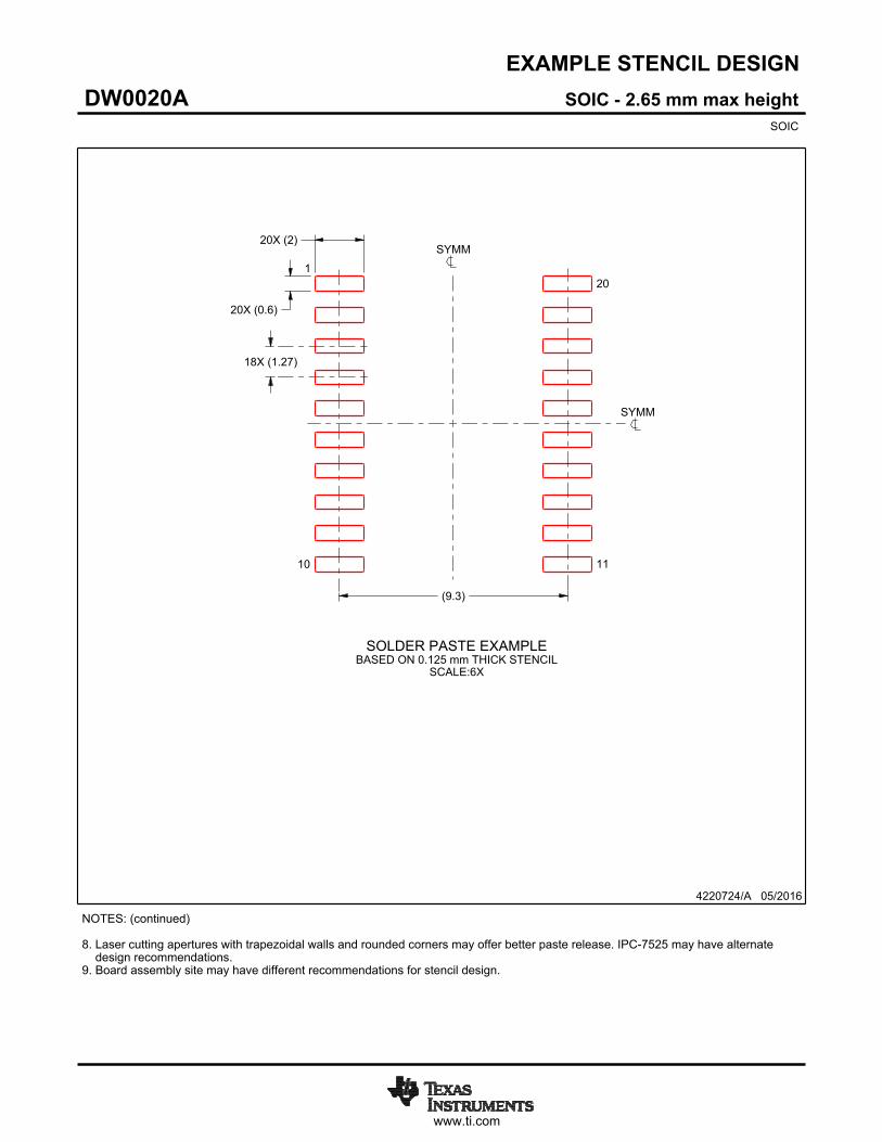
EXAMPLE STENCIL DESIGN
20X (0.6)
20X (0.2)
16X (0.4)
(2.3)
(3.1)
2X (1.07)
(0.525)
(R ) TYP0.05
2X(0.85)
X1QFN - 0.5 mm max heightRWP0020APLASTIC QUAD FLATPACK - NO LEAD
4221912/A 03/2015
NOTES: (continued) 5. Laser cutting apertures with trapezoidal walls and rounded corners may offer better paste release. IPC-7525 may have alternate design recommendations.
SYMM
METALTYP
SOLDER PASTE EXAMPLEBASED ON 0.1 mm THICK STENCIL
EXPOSED PAD
84% PRINTED SOLDER COVERAGE BY AREASCALE:25X
SYMM
1
6
7 10
11
16
1720


www.ti.com
PACKAGE OUTLINE
C
TYP10.639.97
2.65 MAX
18X 1.27
20X 0.510.31
2X11.43
TYP0.330.10
0 - 80.30.1
0.25GAGE PLANE
1.270.40
A
NOTE 3
13.012.6
B 7.67.4
4220724/A 05/2016
SOIC - 2.65 mm max heightDW0020ASOIC
NOTES: 1. All linear dimensions are in millimeters. Dimensions in parenthesis are for reference only. Dimensioning and tolerancing per ASME Y14.5M. 2. This drawing is subject to change without notice. 3. This dimension does not include mold flash, protrusions, or gate burrs. Mold flash, protrusions, or gate burrs shall not exceed 0.15 mm per side. 4. This dimension does not include interlead flash. Interlead flash shall not exceed 0.43 mm per side.5. Reference JEDEC registration MS-013.
120
0.25 C A B
1110
PIN 1 IDAREA
NOTE 4
SEATING PLANE
0.1 C
SEE DETAIL A
DETAIL ATYPICAL
SCALE 1.200

www.ti.com
EXAMPLE BOARD LAYOUT
(9.3)
0.07 MAXALL AROUND
0.07 MINALL AROUND
20X (2)
20X (0.6)
18X (1.27)
(R )TYP
0.05
4220724/A 05/2016
SOIC - 2.65 mm max heightDW0020ASOIC
SYMM
SYMM
LAND PATTERN EXAMPLESCALE:6X
1
10 11
20
NOTES: (continued) 6. Publication IPC-7351 may have alternate designs. 7. Solder mask tolerances between and around signal pads can vary based on board fabrication site.
METALSOLDER MASKOPENING
NON SOLDER MASKDEFINED
SOLDER MASK DETAILS
SOLDER MASKOPENING
METAL UNDERSOLDER MASK
SOLDER MASKDEFINED
www.ti.com
EXAMPLE STENCIL DESIGN
(9.3)
18X (1.27)
20X (0.6)
20X (2)
4220724/A 05/2016
SOIC - 2.65 mm max heightDW0020ASOIC
NOTES: (continued) 8. Laser cutting apertures with trapezoidal walls and rounded corners may offer better paste release. IPC-7525 may have alternate design recommendations. 9. Board assembly site may have different recommendations for stencil design.
SYMM
SYMM
1
10 11
20
SOLDER PASTE EXAMPLEBASED ON 0.125 mm THICK STENCIL
SCALE:6X

IMPORTANT NOTICE
Texas Instruments Incorporated (TI) reserves the right to make corrections, enhancements, improvements and other changes to itssemiconductor products and services per JESD46, latest issue, and to discontinue any product or service per JESD48, latest issue. Buyersshould obtain the latest relevant information before placing orders and should verify that such information is current and complete.TI’s published terms of sale for semiconductor products (http://www.ti.com/sc/docs/stdterms.htm) apply to the sale of packaged integratedcircuit products that TI has qualified and released to market. Additional terms may apply to the use or sale of other types of TI products andservices.Reproduction of significant portions of TI information in TI data sheets is permissible only if reproduction is without alteration and isaccompanied by all associated warranties, conditions, limitations, and notices. TI is not responsible or liable for such reproduceddocumentation. Information of third parties may be subject to additional restrictions. Resale of TI products or services with statementsdifferent from or beyond the parameters stated by TI for that product or service voids all express and any implied warranties for theassociated TI product or service and is an unfair and deceptive business practice. TI is not responsible or liable for any such statements.Buyers and others who are developing systems that incorporate TI products (collectively, “Designers”) understand and agree that Designersremain responsible for using their independent analysis, evaluation and judgment in designing their applications and that Designers havefull and exclusive responsibility to assure the safety of Designers' applications and compliance of their applications (and of all TI productsused in or for Designers’ applications) with all applicable regulations, laws and other applicable requirements. Designer represents that, withrespect to their applications, Designer has all the necessary expertise to create and implement safeguards that (1) anticipate dangerousconsequences of failures, (2) monitor failures and their consequences, and (3) lessen the likelihood of failures that might cause harm andtake appropriate actions. Designer agrees that prior to using or distributing any applications that include TI products, Designer willthoroughly test such applications and the functionality of such TI products as used in such applications.TI’s provision of technical, application or other design advice, quality characterization, reliability data or other services or information,including, but not limited to, reference designs and materials relating to evaluation modules, (collectively, “TI Resources”) are intended toassist designers who are developing applications that incorporate TI products; by downloading, accessing or using TI Resources in anyway, Designer (individually or, if Designer is acting on behalf of a company, Designer’s company) agrees to use any particular TI Resourcesolely for this purpose and subject to the terms of this Notice.TI’s provision of TI Resources does not expand or otherwise alter TI’s applicable published warranties or warranty disclaimers for TIproducts, and no additional obligations or liabilities arise from TI providing such TI Resources. TI reserves the right to make corrections,enhancements, improvements and other changes to its TI Resources. TI has not conducted any testing other than that specificallydescribed in the published documentation for a particular TI Resource.Designer is authorized to use, copy and modify any individual TI Resource only in connection with the development of applications thatinclude the TI product(s) identified in such TI Resource. NO OTHER LICENSE, EXPRESS OR IMPLIED, BY ESTOPPEL OR OTHERWISETO ANY OTHER TI INTELLECTUAL PROPERTY RIGHT, AND NO LICENSE TO ANY TECHNOLOGY OR INTELLECTUAL PROPERTYRIGHT OF TI OR ANY THIRD PARTY IS GRANTED HEREIN, including but not limited to any patent right, copyright, mask work right, orother intellectual property right relating to any combination, machine, or process in which TI products or services are used. Informationregarding or referencing third-party products or services does not constitute a license to use such products or services, or a warranty orendorsement thereof. Use of TI Resources may require a license from a third party under the patents or other intellectual property of thethird party, or a license from TI under the patents or other intellectual property of TI.TI RESOURCES ARE PROVIDED “AS IS” AND WITH ALL FAULTS. TI DISCLAIMS ALL OTHER WARRANTIES ORREPRESENTATIONS, EXPRESS OR IMPLIED, REGARDING RESOURCES OR USE THEREOF, INCLUDING BUT NOT LIMITED TOACCURACY OR COMPLETENESS, TITLE, ANY EPIDEMIC FAILURE WARRANTY AND ANY IMPLIED WARRANTIES OFMERCHANTABILITY, FITNESS FOR A PARTICULAR PURPOSE, AND NON-INFRINGEMENT OF ANY THIRD PARTY INTELLECTUALPROPERTY RIGHTS. TI SHALL NOT BE LIABLE FOR AND SHALL NOT DEFEND OR INDEMNIFY DESIGNER AGAINST ANY CLAIM,INCLUDING BUT NOT LIMITED TO ANY INFRINGEMENT CLAIM THAT RELATES TO OR IS BASED ON ANY COMBINATION OFPRODUCTS EVEN IF DESCRIBED IN TI RESOURCES OR OTHERWISE. IN NO EVENT SHALL TI BE LIABLE FOR ANY ACTUAL,DIRECT, SPECIAL, COLLATERAL, INDIRECT, PUNITIVE, INCIDENTAL, CONSEQUENTIAL OR EXEMPLARY DAMAGES INCONNECTION WITH OR ARISING OUT OF TI RESOURCES OR USE THEREOF, AND REGARDLESS OF WHETHER TI HAS BEENADVISED OF THE POSSIBILITY OF SUCH DAMAGES.Unless TI has explicitly designated an individual product as meeting the requirements of a particular industry standard (e.g., ISO/TS 16949and ISO 26262), TI is not responsible for any failure to meet such industry standard requirements.Where TI specifically promotes products as facilitating functional safety or as compliant with industry functional safety standards, suchproducts are intended to help enable customers to design and create their own applications that meet applicable functional safety standardsand requirements. Using products in an application does not by itself establish any safety features in the application. Designers mustensure compliance with safety-related requirements and standards applicable to their applications. Designer may not use any TI products inlife-critical medical equipment unless authorized officers of the parties have executed a special contract specifically governing such use.Life-critical medical equipment is medical equipment where failure of such equipment would cause serious bodily injury or death (e.g., lifesupport, pacemakers, defibrillators, heart pumps, neurostimulators, and implantables). Such equipment includes, without limitation, allmedical devices identified by the U.S. Food and Drug Administration as Class III devices and equivalent classifications outside the U.S.TI may expressly designate certain products as completing a particular qualification (e.g., Q100, Military Grade, or Enhanced Product).Designers agree that it has the necessary expertise to select the product with the appropriate qualification designation for their applicationsand that proper product selection is at Designers’ own risk. Designers are solely responsible for compliance with all legal and regulatoryrequirements in connection with such selection.Designer will fully indemnify TI and its representatives against any damages, costs, losses, and/or liabilities arising out of Designer’s non-compliance with the terms and provisions of this Notice.
Mailing Address: Texas Instruments, Post Office Box 655303, Dallas, Texas 75265Copyright © 2018, Texas Instruments Incorporated


![Diaz Esther - Metodologia de Las Cs Sociales [Caps 1 2y3]](https://img.pdfslide.net/doc/110x75/55cf9870550346d03397a6ca/diaz-esther-metodologia-de-las-cs-sociales-caps-1-2y3.jpg)