Embed Size (px)
Citation preview

DIR
OE
A1
B1
To Seven Other Channels
2
3
22
21
Product
Folder
Order
Now
Technical
Documents
Tools &
Software
Support &Community
An IMPORTANT NOTICE at the end of this data sheet addresses availability, warranty, changes, use in safety-critical applications,intellectual property matters and other important disclaimers. PRODUCTION DATA.
SN74LVC4245ASCAS375I –MARCH 1994–REVISED JANUARY 2015
SN74LVC4245A Octal Bus Transceiver and 3.3-V to 5-V ShifterWith 3-State Outputs
1
1 Features1• Bidirectional Voltage Translator• 5.5 V on A Port and 2.7 V to 3.6 V on B Port• Control Inputs VIH/VIL Levels Are Referenced to
VCCA Voltage• Latch-Up Performance Exceeds 250 mA Per
JESD 17• ESD Protection Exceeds JESD 22
– 2000-V Human-Body Model– 200-V Machine Model– 1000-V Charged-Device Model
2 Applications• ATCA Solutions• CPAP Machines• Cameras: Surveillance Analog• Chemical or Gas Sensors• CT Scanners• DLP 3D Machine Vision and Optical Networking• Digital Signage• ECGs: Electrocardiograms• Field Transmitters: Pressure Sensors and
Temperature Sensors• High-Speed Data Acquisition and Generation• HMI (Human Machine Interface)• RF4CE Remote Controls• Server Motherboards• Software Defined Radios (SDR)• Wireless LAN Cards and Data Access Cards• X-ray: Medical, Dental, and Baggage Scanners
3 DescriptionThis 8-bit (octal) noninverting bus transceivercontains two separate supply rails; B port has VCCB,which is set at 3.3 V, and A port has VCCA, which isset at 5 V. This allows for translation from a 3.3-V toa 5-V environment, and vice versa.
The SN74LVC4245A device is designed forasynchronous communication between data buses.The device transmits data from the A bus to the Bbus or from the B bus to the A bus, depending on thelogic level at the direction-control (DIR) input. Theoutput-enable (OE) input can be used to disable thedevice so the buses are effectively isolated. Thecontrol circuitry (DIR, OE) is powered by VCCA.
The SN74LVC4245A device terminal out allows thedesigner to switch to a normal all-3.3-V or all-5-V 20-terminal SN74LVC4245 device without board re-layout. The designer uses the data paths for pins2–11 and 14–23 of the SN74LVC4245A device toalign with the conventional '245 terminal out.
Device Information(1)
PART NUMBER PACKAGE BODY SIZE (NOM)
SN74LVC4245ASSOP (24) 8.20 mm × 5.30 mmSOIC (24) 15.40 mm × 7.50 mmTSSOP (24) 7.80 mm × 4.40 mm
(1) For all available packages, see the orderable addendum atthe end of the data sheet.
4 Simplified Schematic

2
SN74LVC4245ASCAS375I –MARCH 1994–REVISED JANUARY 2015 www.ti.com
Product Folder Links: SN74LVC4245A
Submit Documentation Feedback Copyright © 1994–2015, Texas Instruments Incorporated
Table of Contents1 Features .................................................................. 12 Applications ........................................................... 13 Description ............................................................. 14 Simplified Schematic............................................. 15 Revision History..................................................... 26 Pin Configuration and Functions ......................... 37 Specifications......................................................... 4
7.1 Absolute Maximum Ratings ...................................... 47.2 Absolute Maximum Ratings ...................................... 47.3 ESD Ratings.............................................................. 47.4 Recommended Operating Conditions....................... 57.5 Recommended Operating Conditions....................... 57.6 Thermal Information .................................................. 57.7 Electrical Characteristics........................................... 67.8 Electrical Characteristics........................................... 67.9 Switching Characteristics .......................................... 77.10 Operating Characteristics........................................ 77.11 Typical Characteristics ............................................ 7
8 Parameter Measurement Information .................. 88.1 A Port ........................................................................ 8
8.2 B Port ........................................................................ 99 Detailed Description ............................................ 10
9.1 Overview ................................................................. 109.2 Functional Block Diagram ....................................... 109.3 Feature Description................................................. 109.4 Device Functional Modes........................................ 10
10 Application and Implementation........................ 1110.1 Application Information.......................................... 1110.2 Typical Application ............................................... 11
11 Power Supply Recommendations ..................... 1311.1 Power-Up Consideration ...................................... 13
12 Layout................................................................... 1312.1 Layout Guidelines ................................................. 1312.2 Layout Example .................................................... 13
13 Device and Documentation Support ................. 1413.1 Trademarks ........................................................... 1413.2 Electrostatic Discharge Caution............................ 1413.3 Glossary ................................................................ 14
14 Mechanical, Packaging, and OrderableInformation ........................................................... 14
5 Revision History
Changes from Revision H (March 2005) to Revision I Page
• Added Applications, Device Information table, Pin Functions table, ESD Ratings table, Thermal Information table,Typical Characteristics, Feature Description section, Device Functional Modes, Application and Implementationsection, Power Supply Recommendations section, Layout section, Device and Documentation Support section, andMechanical, Packaging, and Orderable Information section. ................................................................................................. 1
• Deleted Ordering Information table. ....................................................................................................................................... 1
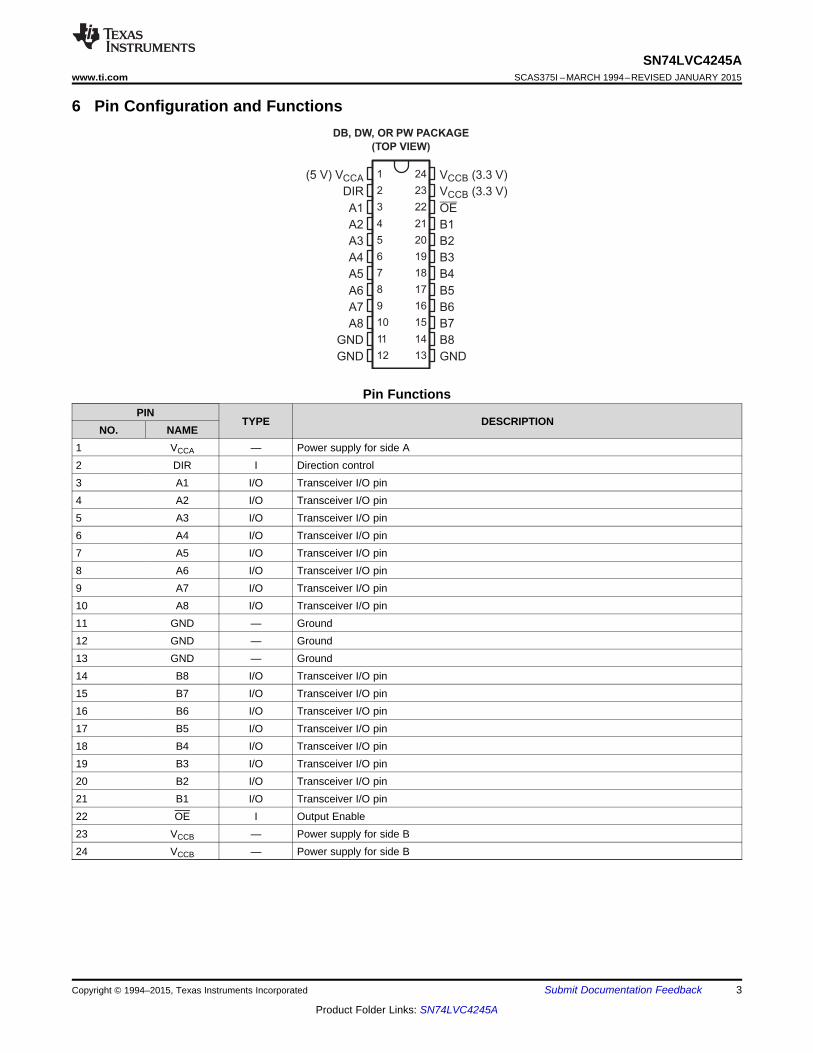
DB, DW, OR PW PACKAGE
(TOP VIEW)
1
2
3
4
5
6
7
8
9
10
11
12
24
23
22
21
20
19
18
17
16
15
14
13
(5 V) VCCA
DIR
A1
A2
A3
A4
A5
A6
A7
A8
GND
GND
VCCB (3.3 V)
VCCB (3.3 V)
OE
B1
B2
B3
B4
B5
B6
B7
B8
GND
3
SN74LVC4245Awww.ti.com SCAS375I –MARCH 1994–REVISED JANUARY 2015
Product Folder Links: SN74LVC4245A
Submit Documentation FeedbackCopyright © 1994–2015, Texas Instruments Incorporated
6 Pin Configuration and Functions
Pin FunctionsPIN
TYPE DESCRIPTIONNO. NAME
1 VCCA — Power supply for side A2 DIR I Direction control3 A1 I/O Transceiver I/O pin4 A2 I/O Transceiver I/O pin5 A3 I/O Transceiver I/O pin6 A4 I/O Transceiver I/O pin7 A5 I/O Transceiver I/O pin8 A6 I/O Transceiver I/O pin9 A7 I/O Transceiver I/O pin10 A8 I/O Transceiver I/O pin11 GND — Ground12 GND — Ground13 GND — Ground14 B8 I/O Transceiver I/O pin15 B7 I/O Transceiver I/O pin16 B6 I/O Transceiver I/O pin17 B5 I/O Transceiver I/O pin18 B4 I/O Transceiver I/O pin19 B3 I/O Transceiver I/O pin20 B2 I/O Transceiver I/O pin21 B1 I/O Transceiver I/O pin22 OE I Output Enable23 VCCB — Power supply for side B24 VCCB — Power supply for side B

4
SN74LVC4245ASCAS375I –MARCH 1994–REVISED JANUARY 2015 www.ti.com
Product Folder Links: SN74LVC4245A
Submit Documentation Feedback Copyright © 1994–2015, Texas Instruments Incorporated
(1) Stresses beyond those listed under Absolute Maximum Ratings may cause permanent damage to the device. These are stress ratingsonly, and functional operation of the device at these or any other conditions beyond those indicated under Recommended OperatingConditions is not implied. Exposure to absolute-maximum-rated conditions for extended periods may affect device reliability.
(2) This value is limited to 6 V maximum.
7 Specifications
7.1 Absolute Maximum Ratingsover operating free-air temperature range for VCCA = 4.5 V to 5.5 V (unless otherwise noted) (1)
MIN MAX UNITVCCA Supply voltage range –0.5 6.5 V
VI Input voltage rangeA port (2) –0.5 VCCA + 0.5
VControl inputs –0.5 6
VO Output voltage range A port (2) –0.5 VCCA + 0.5 VIIK Input clamp current VI < 0 –50 mAIOK Output clamp current VO < 0 –50 mAIO Continuous output current ±50 mA
Continuous current through each VCCA or GND ±100 mATstg Storage temperature range –65 150 °C
(1) Stresses beyond those listed under Absolute Maximum Ratings may cause permanent damage to the device. These are stress ratingsonly, and functional operation of the device at these or any other conditions beyond those indicated under Recommended OperatingConditions is not implied. Exposure to absolute-maximum-rated conditions for extended periods may affect device reliability.
(2) This value is limited to 4.6 V maximum.
7.2 Absolute Maximum Ratingsover operating free-air temperature range for VCCB = 2.7 V to 3.6 V (unless otherwise noted) (1)
MIN MAX UNITVCCB Supply voltage range –0.5 4.6 VVI Input voltage range B port (2) –0.5 VCCB + 0.5 VVO Output voltage range B port (2) –0.5 VCCB + 0.5 VIIK Input clamp current VI < 0 –50 mAIOK Output clamp current VO < 0 –50 mAIO Continuous output current ±50 mA
Continuous current through VCCB or GND ±100 mATstg Storage temperature range –65 150 °C
(1) JEDEC document JEP155 states that 500-V HBM allows safe manufacturing with a standard ESD control process.(2) JEDEC document JEP157 states that 250-V CDM allows safe manufacturing with a standard ESD control process.
7.3 ESD RatingsPARAMETER DEFINITION VALUE UNIT
V(ESD)Electrostaticdischarge
Human body model (HBM), per ANSI/ESDA/JEDEC JS-001, all pins (1) 2000V
Charged device model (CDM), per JEDEC specification JESD22-C101, all pins (2) 1000
5
SN74LVC4245Awww.ti.com SCAS375I –MARCH 1994–REVISED JANUARY 2015
Product Folder Links: SN74LVC4245A
Submit Documentation FeedbackCopyright © 1994–2015, Texas Instruments Incorporated
(1) All unused inputs of the device must be held at the associated VCC or GND to ensure proper device operation. Refer to the TIapplication report, Implications of Slow or Floating CMOS Inputs, literature number SCBA004.
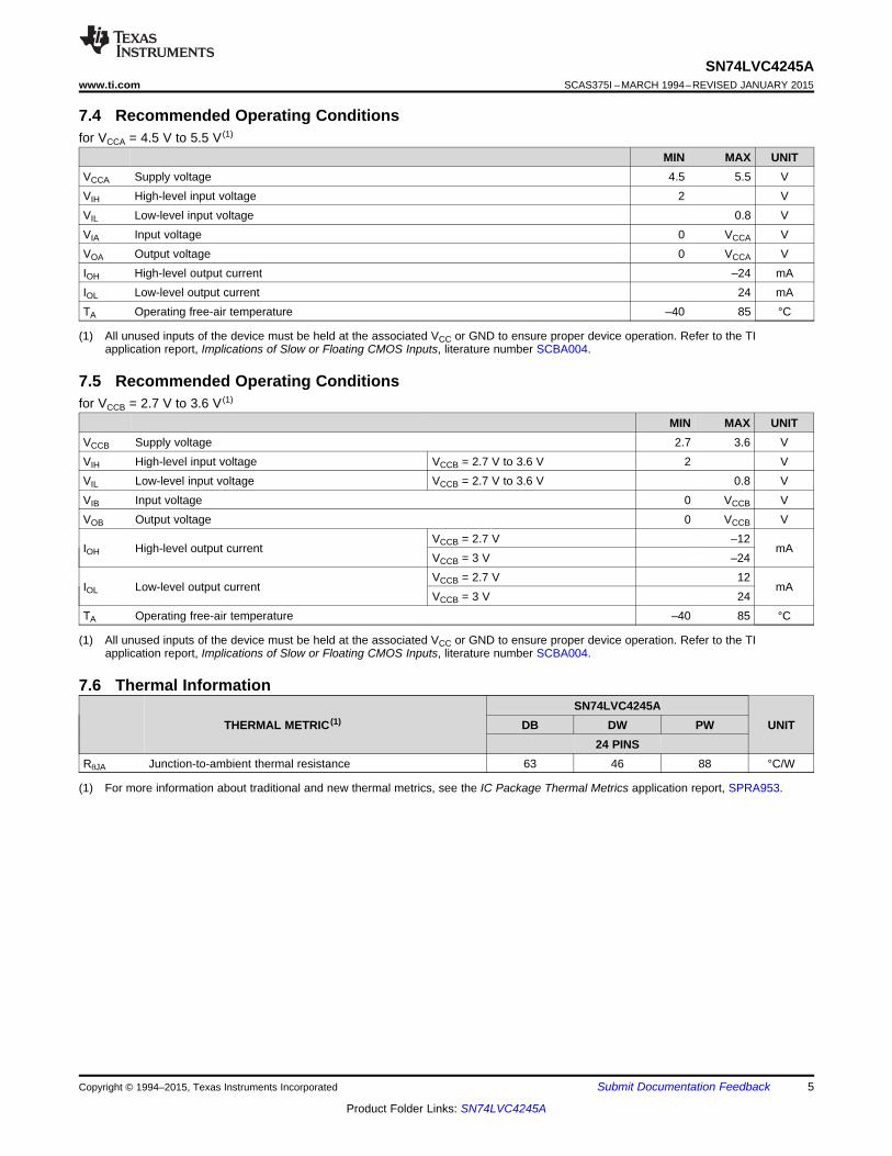
7.4 Recommended Operating Conditionsfor VCCA = 4.5 V to 5.5 V (1)
MIN MAX UNITVCCA Supply voltage 4.5 5.5 VVIH High-level input voltage 2 VVIL Low-level input voltage 0.8 VVIA Input voltage 0 VCCA VVOA Output voltage 0 VCCA VIOH High-level output current –24 mAIOL Low-level output current 24 mATA Operating free-air temperature –40 85 °C
(1) All unused inputs of the device must be held at the associated VCC or GND to ensure proper device operation. Refer to the TIapplication report, Implications of Slow or Floating CMOS Inputs, literature number SCBA004.
7.5 Recommended Operating Conditionsfor VCCB = 2.7 V to 3.6 V (1)
MIN MAX UNITVCCB Supply voltage 2.7 3.6 VVIH High-level input voltage VCCB = 2.7 V to 3.6 V 2 VVIL Low-level input voltage VCCB = 2.7 V to 3.6 V 0.8 VVIB Input voltage 0 VCCB VVOB Output voltage 0 VCCB V
IOH High-level output currentVCCB = 2.7 V –12
mAVCCB = 3 V –24
IOL Low-level output currentVCCB = 2.7 V 12
mAVCCB = 3 V 24
TA Operating free-air temperature –40 85 °C
(1) For more information about traditional and new thermal metrics, see the IC Package Thermal Metrics application report, SPRA953.
7.6 Thermal Information
THERMAL METRIC (1)SN74LVC4245A
UNITDB DW PW24 PINS
RθJA Junction-to-ambient thermal resistance 63 46 88 °C/W

6
SN74LVC4245ASCAS375I –MARCH 1994–REVISED JANUARY 2015 www.ti.com
Product Folder Links: SN74LVC4245A
Submit Documentation Feedback Copyright © 1994–2015, Texas Instruments Incorporated
(1) VCCB = 2.7 V to 3.6 V.(2) All typical values are measured at VCC = 5 V, TA = 25°C.(3) For I/O ports, the parameter IOZ includes the input leakage current.(4) This is the increase in supply current for each input that is at one of the specified TTL voltage levels, rather than 0 V or the associated
VCC.
7.7 Electrical Characteristicsover recommended operating free-air temperature range for VCCA = 4.5 V to 5.5 V (unless otherwise noted) (1)
PARAMETER TEST CONDITIONS VCCA MIN TYP (2) MAX UNIT
VOH
IOH = –100 μA4.5 V 4.3
V5.5 V 5.3
IOH = –24 mA4.5 V 3.75.5 V 4.7
VOL
IOL = 100 μA4.5 V 0.2
V5.5 V 0.2
IOL = 24 mA4.5 V 0.555.5 V 0.55
II Control inputs VI = VCCA or GND 5.5 V ±1 μAIOZ
(3) A port VO = VCCA or GND 5.5 V ±5 μAICCA VI = VCCA or GND, IO = 0 5.5 V 80 μAΔICCA
(4) One input at 3.4 V, Other inputs at VCCA or GND 5.5 V 1.5 mACi Control inputs VI = VCCA or GND Open 5 pFCio A port VO = VCCA or GND 5 V 11 pF
(1) VCCA = 5 V ± 0.5 V.(2) All typical values are measured at VCC = 3.3 V, TA = 25°C.(3) For I/O ports, the parameter IOZ includes the input leakage current.(4) This is the increase in supply current for each input that is at one of the specified TTL voltage levels, rather than 0 V or the associated
VCC.
7.8 Electrical Characteristicsover recommended operating free-air temperature range for VCCB = 2.7 V to 3.6 V (unless otherwise noted) (1)
PARAMETER TEST CONDITIONS VCCB MIN TYP (2) MAX UNIT
VOH
IOH = –100 μA 2.7 V to 3.6 V VCC – 0.2
VIOH = –12 mA2.7 V 2.23 V 2.4
IOH = –24 mA 3 V 2
VOL
IOL = 100 μA 2.7 V to 3.6 V 0.2VIOL = 12 mA 2.7 V 0.4
IOL = 24 mA 3 V 0.55IOZ
(3) B port VO = VCCB or GND 3.6 V ±5 μAICCB VI = VCCB or GND, IO = 0 3.6 V 50 μA
ΔICCB(4) One input at VCCB – 0.6
V, Other inputs at VCCB or GND 2.7 V to 3.6 V 0.5 mA
Cio B port VO = VCCB or GND 3.3 V 11 pF

2
4
6
8
10
12
14
0 50 100 150 200 250 300
CL – Load Capacitance – pF
VCC = 3 V,
TA = 25°C
One Output Switching
Four Outputs Switching
Eight Outputs Switching
t–
Pro
pag
ati
on
Dela
yT
ime
–n
sp
d
2
4
6
8
10
0 50 100 150 200 250 300
CL – Load Capacitance – pF
t–
Pro
pa
ga
tio
nD
ela
yT
ime
–n
sp
d
VCC = 3 V,
TA = 25°C
One Output Switching
Four Outputs Switching
Eight Outputs Switching
7
SN74LVC4245Awww.ti.com SCAS375I –MARCH 1994–REVISED JANUARY 2015
Product Folder Links: SN74LVC4245A
Submit Documentation FeedbackCopyright © 1994–2015, Texas Instruments Incorporated
7.9 Switching Characteristicsover recommended operating free-air temperature range, CL = 50 pF (unless otherwise noted) (see Figure 3 and Figure 4)
PARAMETER FROM(INPUT)
TO(OUTPUT)
VCCA = 5 V ± 0.5 V,VCCB = 2.7 V to 3.6 V UNIT
MIN MAXtPHL A B
1 6.3ns
tPLH 1 6.7tPHL B A
1 6.1ns
tPLH 1 5tPZL OE A
1 9ns
tPZH 1 8.1tPZL OE B
1 8.8ns
tPZH 1 9.8tPLZ OE A
1 7ns
tPHZ 1 5.8tPLZ OE B
1 7.7ns
tPHZ 1 7.8
7.10 Operating CharacteristicsVCCA = 4.5 V to 5.5 V, VCCB = 2.7 V to 3.6 V, TA = 25°C
PARAMETER TEST CONDITIONS TYP UNIT
Cpd Power dissipation capacitance per transceiverOutputs enabled
CL = 0, f = 10 MHz39.5
pFOutputs disabled 5
7.11 Typical Characteristics
Figure 1. Propagation Delay (Low to High Transition)vs Load Capacitance
Figure 2. Propagation Delay (High to Low Transition)vs Load Capacitance

From Output
Under Test
CL = 50 pF
(see Note A)
LOAD CIRCUIT
S1
2 × VCC
Open
GND
500 Ω
500 Ω
VOLTAGE WAVEFORMS
PROPAGATION DELAY TIMES
NONINVERTING OUTPUTS
tPLH tPHL
VOH
VOL
Output
Control
Output
Waveform 1
S1 at 2 × VCC
(see Note B)
Output
Waveform 2
S1 at GND
(see Note B)
VOL
VOH
tPZL
tPZH
tPLZ
tPHZ
1.5 V1.5 V
VCC
0 V
VOL + 0.3 V
VOH - 0.3 V
≈0 V
3 V
VOLTAGE WAVEFORMS
ENABLE AND DISABLE TIMES
LOW- AND HIGH-LEVEL ENABLING
Output
tPLH/tPHL
tPLZ/tPZL
tPHZ/tPZH
Open
2 × VCC
GND
TEST S1
NOTES: A. CL includes probe and jig capacitance.
B. Waveform 1 is for an output with internal conditions such that the output is low, except when disabled by the output control.
Waveform 2 is for an output with internal conditions such that the output is high, except when disabled by the output control.
C. All input pulses are supplied by generators having the following characteristics: PRR≤ 10 MHz, ZO = 50 Ω, tr ≤ 2.5 ns, tf ≤ 2.5 ns.
D. The outputs are measured one at a time, with one transition per measurement.
E. All parameters and waveforms are not applicable to all devices.
VCC
0 V
1.5 VInput
50% VCC
50% VCC
50% VCC
1.5 V
50% VCC
VCC
0 V
1.5 V 1.5 V
t
Input
w
VOLTAGE WAVEFORMS
PULSE DURATION
8
SN74LVC4245ASCAS375I –MARCH 1994–REVISED JANUARY 2015 www.ti.com
Product Folder Links: SN74LVC4245A
Submit Documentation Feedback Copyright © 1994–2015, Texas Instruments Incorporated
8 Parameter Measurement Information
8.1 A Port
Figure 3. Load Circuit and Voltage Waveforms

From Output
Under Test
CL = 50 pF
(see Note A)
LOAD CIRCUIT
S1
7 V
Open
GND
500 Ω
500 Ω
VOLTAGE WAVEFORMS
PROPAGATION DELAY TIMES
NONINVERTING OUTPUTS
tPLH tPHL
VOH
VOL
Output
Control
Output
Waveform 1
S1 at 7 V
(see Note B)
Output
Waveform 2
S1 at GND
(see Note B)
VOL
VOH
tPZL
tPZH
tPLZ
tPHZ
1.5 V1.5 V
3.5 V
0 V
VOL + 0.3 V
VOH - 0.3 V
≈0 V
3 V
VOLTAGE WAVEFORMS
ENABLE AND DISABLE TIMES
LOW- AND HIGH-LEVEL ENABLING
Output
tPLH/tPHL
tPLZ/tPZL
tPHZ/tPZH
Open
7 V
GND
TEST S1
NOTES: A. CL includes probe and jig capacitance.
B. Waveform 1 is for an output with internal conditions such that the output is low, except when disabled by the output control.
Waveform 2 is for an output with internal conditions such that the output is high, except when disabled by the output control.
C. All input pulses are supplied by generators having the following characteristics: PRR≤ 10 MHz, ZO = 50 Ω, tr ≤ 2.5 ns, tf ≤ 2.5 ns.
D. The outputs are measured one at a time, with one transition per measurement.
E. All parameters and waveforms are not applicable to all devices.
3 V
0 V
1.5 VInput 1.5 V
1.5 V 1.5 V
1.5 V
1.5 V
3 V
0 V
1.5 V 1.5 V
t
Input
w
VOLTAGE WAVEFORMS
PULSE DURATION
9
SN74LVC4245Awww.ti.com SCAS375I –MARCH 1994–REVISED JANUARY 2015
Product Folder Links: SN74LVC4245A
Submit Documentation FeedbackCopyright © 1994–2015, Texas Instruments Incorporated
8.2 B Port
Figure 4. Load Circuit and Voltage Waveforms

DIR
OE
A1
B1
To Seven Other Channels
2
3
22
21
10
SN74LVC4245ASCAS375I –MARCH 1994–REVISED JANUARY 2015 www.ti.com
Product Folder Links: SN74LVC4245A
Submit Documentation Feedback Copyright © 1994–2015, Texas Instruments Incorporated
9 Detailed Description
9.1 OverviewSN74LVC4245A is an 8-bit (octal) noninverting bus transceiver contains two separate supply rails; B port hasVCCB, which is set at 3.3 V, and A port has VCCA, which is set at 5 V. This allows for translation from a 3.3-V to a5-V environment, and vice versa, designed for asynchronous communication between data buses. The devicetransmits data from the A bus to the B bus or from the B bus to the A bus, depending on the logic level at thedirection-control (DIR) input. The output-enable (OE) input can be used to disable the device so the buses areeffectively isolated. The control circuitry (DIR, OE) is powered by VCCA.
9.2 Functional Block Diagram
Figure 5. Logic Diagram (Positive Logic)
9.3 Feature Description• 24 mA drive at 3-V supply
– Good for heavier loads and longer traces• Low VIH
– Allows 3.3-V to 5-V translation
9.4 Device Functional Modes
Function TableINPUTS
OPERATIONOE DIRL L B data to A busL H A data to B busH X Isolation

C or System Logic A1
A8
B1
B8
VCCB
GND
C/System Logic/LEDs
3 V5 V
OE
VCCA
DIR
11
SN74LVC4245Awww.ti.com SCAS375I –MARCH 1994–REVISED JANUARY 2015
Product Folder Links: SN74LVC4245A
Submit Documentation FeedbackCopyright © 1994–2015, Texas Instruments Incorporated
10 Application and Implementation
10.1 Application InformationThe SN74LVC4245A device pinout allows the designer to switch to a normal all-3.3-V or all-5-V 20-pin '245device without board re-layout. The designer uses the data paths for pins 2–11 and 14–23 of theSN74LVC4245A to align with the conventional SN74LVC4245 device's pinout. SN74LVC4245A is a high driveCMOS device that can be used for a multitude of bus interface type applications where output drive or PCB tracelength is a concern.
10.2 Typical Application
Figure 6. Typical Application Schematic
10.2.1 Design RequirementsThis device uses CMOS technology and has balanced output drive. Care should be taken to avoid buscontention because it can drive currents that would exceed maximum limits. The high drive will also create fastedges into light loads so routing and load conditions should be considered to prevent ringing.
10.2.2 Detailed Design Procedure1. Recommended Input Conditions:
– For rise time and fall time specifcations, see (Δt/ΔV) in the Recommended Operating Conditions table.– For specified high and low levels, see (VIH and VIL) in the Recommended Operating Conditions table.
2. Recommend Output Conditions:– Load currents should not exceed (IO max) per output and should not exceed (Continuous current through
VCC or GND) total current for the part. These limits are located in the Absolute Maximum Ratings table.– Outputs should not be pulled above VCC.– Series resistors on the output may be used if the user desires to slow the output edge signal or limit the
output current.

–100
–80
–60
–40
–20
0
20
40
60
–1 –0.5 0.0 0.5 1.0 1.5 2.0 2.5 3.0 3.5 4.0
TA = 25°C, VCC = 3 V,
VIH = 3 V, VIL = 0 V,
All Outputs Switching
VOH – VI O
H–
mA
VOL – V
–20
0
20
40
60
80
100
–0.2 0.0 0.2 0.4 0.6 0.8 1.0 1.2 1.4 1.6
TA = 25°C, VCC = 3 V,
VIH = 3 V, VIL = 0 V,
All Outputs Switching
I OL
–m
A
12
SN74LVC4245ASCAS375I –MARCH 1994–REVISED JANUARY 2015 www.ti.com
Product Folder Links: SN74LVC4245A
Submit Documentation Feedback Copyright © 1994–2015, Texas Instruments Incorporated
Typical Application (continued)10.2.3 Application Curves
Figure 7. Output Drive Current (IOL)vs LOW-level Output Voltage (VOL)
Figure 8. Output Drive Current (IOH)vs HIGH-level Output Voltage (VOH)

VCC
Unused Input
Input
Output Output
Input
Unused Input
13
SN74LVC4245Awww.ti.com SCAS375I –MARCH 1994–REVISED JANUARY 2015
Product Folder Links: SN74LVC4245A
Submit Documentation FeedbackCopyright © 1994–2015, Texas Instruments Incorporated
(1) Refer to the TI application report, Texas Instruments Voltage-Level-Translation Devices, literature number SCEA021.
11 Power Supply Recommendations
11.1 Power-Up Consideration(1)TI level-translation devices offer an opportunity for successful mixed-voltage signal design. A proper power-upsequence always should be followed to avoid excessive supply current, bus contention, oscillations, or otheranomalies caused by improperly biased device terminals. Take these precautions to guard against such power-up problems:1. Connect ground before any supply voltage is applied.2. Power up the control side of the device (VCCA for all four of these devices).3. Tie OE to VCCA with a pullup resistor so that it ramps with VCCA.4. Depending on the direction of the data path, DIR can be high or low. If DIR high is needed (A data to B bus),
ramp it with VCCA. Otherwise, keep DIR low.
12 Layout
12.1 Layout GuidelinesWhen using multiple bit logic devices, inputs should not float. In many cases, functions or parts of functions ofdigital logic devices are unused. Some examples are when only two inputs of a triple-input AND gate are used,or when only 3 of the 4-buffer gates are used. Such input pins should not be left unconnected because theundefined voltages at the outside connections result in undefined operational states.
Specified in Figure 9 are rules that must be observed under all circumstances. All unused inputs of digital logicdevices must be connected to a high or low bias to prevent them from floating. The logic level that should beapplied to any particular unused input depends on the function of the device. Generally they will be tied to GNDor VCC, whichever makes more sense or is more convenient.
12.2 Layout Example
Figure 9. Layout Diagram

14
SN74LVC4245ASCAS375I –MARCH 1994–REVISED JANUARY 2015 www.ti.com
Product Folder Links: SN74LVC4245A
Submit Documentation Feedback Copyright © 1994–2015, Texas Instruments Incorporated
13 Device and Documentation Support
13.1 TrademarksAll trademarks are the property of their respective owners.
13.2 Electrostatic Discharge CautionThese devices have limited built-in ESD protection. The leads should be shorted together or the device placed in conductive foamduring storage or handling to prevent electrostatic damage to the MOS gates.
13.3 GlossarySLYZ022 — TI Glossary.
This glossary lists and explains terms, acronyms, and definitions.
14 Mechanical, Packaging, and Orderable InformationThe following pages include mechanical, packaging, and orderable information. This information is the mostcurrent data available for the designated devices. This data is subject to change without notice and revision ofthis document. For browser-based versions of this data sheet, refer to the left-hand navigation.
PACKAGE OPTION ADDENDUM
www.ti.com 10-Jun-2014
Addendum-Page 1
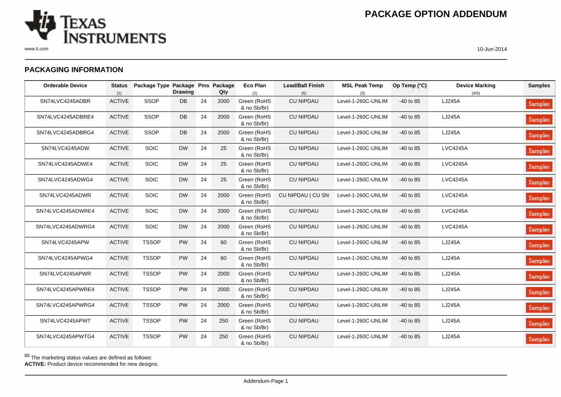
PACKAGING INFORMATION
Orderable Device Status(1)
Package Type PackageDrawing
Pins PackageQty
Eco Plan(2)
Lead/Ball Finish(6)
MSL Peak Temp(3)
Op Temp (°C) Device Marking(4/5)
Samples
SN74LVC4245ADBR ACTIVE SSOP DB 24 2000 Green (RoHS& no Sb/Br)
CU NIPDAU Level-1-260C-UNLIM -40 to 85 LJ245A
SN74LVC4245ADBRE4 ACTIVE SSOP DB 24 2000 Green (RoHS& no Sb/Br)
CU NIPDAU Level-1-260C-UNLIM -40 to 85 LJ245A
SN74LVC4245ADBRG4 ACTIVE SSOP DB 24 2000 Green (RoHS& no Sb/Br)
CU NIPDAU Level-1-260C-UNLIM -40 to 85 LJ245A
SN74LVC4245ADW ACTIVE SOIC DW 24 25 Green (RoHS& no Sb/Br)
CU NIPDAU Level-1-260C-UNLIM -40 to 85 LVC4245A
SN74LVC4245ADWE4 ACTIVE SOIC DW 24 25 Green (RoHS& no Sb/Br)
CU NIPDAU Level-1-260C-UNLIM -40 to 85 LVC4245A
SN74LVC4245ADWG4 ACTIVE SOIC DW 24 25 Green (RoHS& no Sb/Br)
CU NIPDAU Level-1-260C-UNLIM -40 to 85 LVC4245A
SN74LVC4245ADWR ACTIVE SOIC DW 24 2000 Green (RoHS& no Sb/Br)
CU NIPDAU | CU SN Level-1-260C-UNLIM -40 to 85 LVC4245A
SN74LVC4245ADWRE4 ACTIVE SOIC DW 24 2000 Green (RoHS& no Sb/Br)
CU NIPDAU Level-1-260C-UNLIM -40 to 85 LVC4245A
SN74LVC4245ADWRG4 ACTIVE SOIC DW 24 2000 Green (RoHS& no Sb/Br)
CU NIPDAU Level-1-260C-UNLIM -40 to 85 LVC4245A
SN74LVC4245APW ACTIVE TSSOP PW 24 60 Green (RoHS& no Sb/Br)
CU NIPDAU Level-1-260C-UNLIM -40 to 85 LJ245A
SN74LVC4245APWG4 ACTIVE TSSOP PW 24 60 Green (RoHS& no Sb/Br)
CU NIPDAU Level-1-260C-UNLIM -40 to 85 LJ245A
SN74LVC4245APWR ACTIVE TSSOP PW 24 2000 Green (RoHS& no Sb/Br)
CU NIPDAU Level-1-260C-UNLIM -40 to 85 LJ245A
SN74LVC4245APWRE4 ACTIVE TSSOP PW 24 2000 Green (RoHS& no Sb/Br)
CU NIPDAU Level-1-260C-UNLIM -40 to 85 LJ245A
SN74LVC4245APWRG4 ACTIVE TSSOP PW 24 2000 Green (RoHS& no Sb/Br)
CU NIPDAU Level-1-260C-UNLIM -40 to 85 LJ245A
SN74LVC4245APWT ACTIVE TSSOP PW 24 250 Green (RoHS& no Sb/Br)
CU NIPDAU Level-1-260C-UNLIM -40 to 85 LJ245A
SN74LVC4245APWTG4 ACTIVE TSSOP PW 24 250 Green (RoHS& no Sb/Br)
CU NIPDAU Level-1-260C-UNLIM -40 to 85 LJ245A
(1) The marketing status values are defined as follows:ACTIVE: Product device recommended for new designs.

PACKAGE OPTION ADDENDUM
www.ti.com 10-Jun-2014
Addendum-Page 2
LIFEBUY: TI has announced that the device will be discontinued, and a lifetime-buy period is in effect.NRND: Not recommended for new designs. Device is in production to support existing customers, but TI does not recommend using this part in a new design.PREVIEW: Device has been announced but is not in production. Samples may or may not be available.OBSOLETE: TI has discontinued the production of the device.
(2) Eco Plan - The planned eco-friendly classification: Pb-Free (RoHS), Pb-Free (RoHS Exempt), or Green (RoHS & no Sb/Br) - please check http://www.ti.com/productcontent for the latest availabilityinformation and additional product content details.TBD: The Pb-Free/Green conversion plan has not been defined.Pb-Free (RoHS): TI's terms "Lead-Free" or "Pb-Free" mean semiconductor products that are compatible with the current RoHS requirements for all 6 substances, including the requirement thatlead not exceed 0.1% by weight in homogeneous materials. Where designed to be soldered at high temperatures, TI Pb-Free products are suitable for use in specified lead-free processes.Pb-Free (RoHS Exempt): This component has a RoHS exemption for either 1) lead-based flip-chip solder bumps used between the die and package, or 2) lead-based die adhesive used betweenthe die and leadframe. The component is otherwise considered Pb-Free (RoHS compatible) as defined above.Green (RoHS & no Sb/Br): TI defines "Green" to mean Pb-Free (RoHS compatible), and free of Bromine (Br) and Antimony (Sb) based flame retardants (Br or Sb do not exceed 0.1% by weightin homogeneous material)
(3) MSL, Peak Temp. - The Moisture Sensitivity Level rating according to the JEDEC industry standard classifications, and peak solder temperature.
(4) There may be additional marking, which relates to the logo, the lot trace code information, or the environmental category on the device.
(5) Multiple Device Markings will be inside parentheses. Only one Device Marking contained in parentheses and separated by a "~" will appear on a device. If a line is indented then it is a continuationof the previous line and the two combined represent the entire Device Marking for that device.
(6) Lead/Ball Finish - Orderable Devices may have multiple material finish options. Finish options are separated by a vertical ruled line. Lead/Ball Finish values may wrap to two lines if the finishvalue exceeds the maximum column width.
Important Information and Disclaimer:The information provided on this page represents TI's knowledge and belief as of the date that it is provided. TI bases its knowledge and belief on informationprovided by third parties, and makes no representation or warranty as to the accuracy of such information. Efforts are underway to better integrate information from third parties. TI has taken andcontinues to take reasonable steps to provide representative and accurate information but may not have conducted destructive testing or chemical analysis on incoming materials and chemicals.TI and TI suppliers consider certain information to be proprietary, and thus CAS numbers and other limited information may not be available for release.
In no event shall TI's liability arising out of such information exceed the total purchase price of the TI part(s) at issue in this document sold by TI to Customer on an annual basis.
OTHER QUALIFIED VERSIONS OF SN74LVC4245A :
• Enhanced Product: SN74LVC4245A-EP
NOTE: Qualified Version Definitions:
• Enhanced Product - Supports Defense, Aerospace and Medical Applications

TAPE AND REEL INFORMATION
*All dimensions are nominal
Device PackageType
PackageDrawing
Pins SPQ ReelDiameter
(mm)
ReelWidth
W1 (mm)
A0(mm)
B0(mm)
K0(mm)
P1(mm)
W(mm)
Pin1Quadrant
SN74LVC4245ADBR SSOP DB 24 2000 330.0 16.4 8.2 8.8 2.5 12.0 16.0 Q1
SN74LVC4245ADWR SOIC DW 24 2000 330.0 24.4 10.75 15.7 2.7 12.0 24.0 Q1
SN74LVC4245ADWR SOIC DW 24 2000 330.0 24.4 10.75 15.7 2.7 12.0 24.0 Q1
SN74LVC4245ADWRG4 SOIC DW 24 2000 330.0 24.4 10.75 15.7 2.7 12.0 24.0 Q1
SN74LVC4245APWR TSSOP PW 24 2000 330.0 16.4 6.95 8.3 1.6 8.0 16.0 Q1
SN74LVC4245APWT TSSOP PW 24 250 330.0 16.4 6.95 8.3 1.6 8.0 16.0 Q1
PACKAGE MATERIALS INFORMATION
www.ti.com 25-Jun-2015
Pack Materials-Page 1

*All dimensions are nominal
Device Package Type Package Drawing Pins SPQ Length (mm) Width (mm) Height (mm)
SN74LVC4245ADBR SSOP DB 24 2000 367.0 367.0 38.0
SN74LVC4245ADWR SOIC DW 24 2000 367.0 367.0 45.0
SN74LVC4245ADWR SOIC DW 24 2000 364.0 361.0 36.0
SN74LVC4245ADWRG4 SOIC DW 24 2000 367.0 367.0 45.0
SN74LVC4245APWR TSSOP PW 24 2000 367.0 367.0 38.0
SN74LVC4245APWT TSSOP PW 24 250 367.0 367.0 38.0
PACKAGE MATERIALS INFORMATION
www.ti.com 25-Jun-2015
Pack Materials-Page 2


MECHANICAL DATA
MSSO002E – JANUARY 1995 – REVISED DECEMBER 2001
POST OFFICE BOX 655303 • DALLAS, TEXAS 75265
DB (R-PDSO-G**) PLASTIC SMALL-OUTLINE
4040065 /E 12/01
28 PINS SHOWN
Gage Plane
8,207,40
0,550,95
0,25
38
12,90
12,30
28
10,50
24
8,50
Seating Plane
9,907,90
30
10,50
9,90
0,38
5,605,00
15
0,22
14
A
28
1
2016
6,506,50
14
0,05 MIN
5,905,90
DIM
A MAX
A MIN
PINS **
2,00 MAX
6,90
7,50
0,65 M0,15
0°–8°
0,10
0,090,25
NOTES: A. All linear dimensions are in millimeters.B. This drawing is subject to change without notice.C. Body dimensions do not include mold flash or protrusion not to exceed 0,15.D. Falls within JEDEC MO-150

IMPORTANT NOTICE
Texas Instruments Incorporated (TI) reserves the right to make corrections, enhancements, improvements and other changes to itssemiconductor products and services per JESD46, latest issue, and to discontinue any product or service per JESD48, latest issue. Buyersshould obtain the latest relevant information before placing orders and should verify that such information is current and complete.TI’s published terms of sale for semiconductor products (http://www.ti.com/sc/docs/stdterms.htm) apply to the sale of packaged integratedcircuit products that TI has qualified and released to market. Additional terms may apply to the use or sale of other types of TI products andservices.Reproduction of significant portions of TI information in TI data sheets is permissible only if reproduction is without alteration and isaccompanied by all associated warranties, conditions, limitations, and notices. TI is not responsible or liable for such reproduceddocumentation. Information of third parties may be subject to additional restrictions. Resale of TI products or services with statementsdifferent from or beyond the parameters stated by TI for that product or service voids all express and any implied warranties for theassociated TI product or service and is an unfair and deceptive business practice. TI is not responsible or liable for any such statements.Buyers and others who are developing systems that incorporate TI products (collectively, “Designers”) understand and agree that Designersremain responsible for using their independent analysis, evaluation and judgment in designing their applications and that Designers havefull and exclusive responsibility to assure the safety of Designers' applications and compliance of their applications (and of all TI productsused in or for Designers’ applications) with all applicable regulations, laws and other applicable requirements. Designer represents that, withrespect to their applications, Designer has all the necessary expertise to create and implement safeguards that (1) anticipate dangerousconsequences of failures, (2) monitor failures and their consequences, and (3) lessen the likelihood of failures that might cause harm andtake appropriate actions. Designer agrees that prior to using or distributing any applications that include TI products, Designer willthoroughly test such applications and the functionality of such TI products as used in such applications.TI’s provision of technical, application or other design advice, quality characterization, reliability data or other services or information,including, but not limited to, reference designs and materials relating to evaluation modules, (collectively, “TI Resources”) are intended toassist designers who are developing applications that incorporate TI products; by downloading, accessing or using TI Resources in anyway, Designer (individually or, if Designer is acting on behalf of a company, Designer’s company) agrees to use any particular TI Resourcesolely for this purpose and subject to the terms of this Notice.TI’s provision of TI Resources does not expand or otherwise alter TI’s applicable published warranties or warranty disclaimers for TIproducts, and no additional obligations or liabilities arise from TI providing such TI Resources. TI reserves the right to make corrections,enhancements, improvements and other changes to its TI Resources. TI has not conducted any testing other than that specificallydescribed in the published documentation for a particular TI Resource.Designer is authorized to use, copy and modify any individual TI Resource only in connection with the development of applications thatinclude the TI product(s) identified in such TI Resource. NO OTHER LICENSE, EXPRESS OR IMPLIED, BY ESTOPPEL OR OTHERWISETO ANY OTHER TI INTELLECTUAL PROPERTY RIGHT, AND NO LICENSE TO ANY TECHNOLOGY OR INTELLECTUAL PROPERTYRIGHT OF TI OR ANY THIRD PARTY IS GRANTED HEREIN, including but not limited to any patent right, copyright, mask work right, orother intellectual property right relating to any combination, machine, or process in which TI products or services are used. Informationregarding or referencing third-party products or services does not constitute a license to use such products or services, or a warranty orendorsement thereof. Use of TI Resources may require a license from a third party under the patents or other intellectual property of thethird party, or a license from TI under the patents or other intellectual property of TI.TI RESOURCES ARE PROVIDED “AS IS” AND WITH ALL FAULTS. TI DISCLAIMS ALL OTHER WARRANTIES ORREPRESENTATIONS, EXPRESS OR IMPLIED, REGARDING RESOURCES OR USE THEREOF, INCLUDING BUT NOT LIMITED TOACCURACY OR COMPLETENESS, TITLE, ANY EPIDEMIC FAILURE WARRANTY AND ANY IMPLIED WARRANTIES OFMERCHANTABILITY, FITNESS FOR A PARTICULAR PURPOSE, AND NON-INFRINGEMENT OF ANY THIRD PARTY INTELLECTUALPROPERTY RIGHTS. TI SHALL NOT BE LIABLE FOR AND SHALL NOT DEFEND OR INDEMNIFY DESIGNER AGAINST ANY CLAIM,INCLUDING BUT NOT LIMITED TO ANY INFRINGEMENT CLAIM THAT RELATES TO OR IS BASED ON ANY COMBINATION OFPRODUCTS EVEN IF DESCRIBED IN TI RESOURCES OR OTHERWISE. IN NO EVENT SHALL TI BE LIABLE FOR ANY ACTUAL,DIRECT, SPECIAL, COLLATERAL, INDIRECT, PUNITIVE, INCIDENTAL, CONSEQUENTIAL OR EXEMPLARY DAMAGES INCONNECTION WITH OR ARISING OUT OF TI RESOURCES OR USE THEREOF, AND REGARDLESS OF WHETHER TI HAS BEENADVISED OF THE POSSIBILITY OF SUCH DAMAGES.Unless TI has explicitly designated an individual product as meeting the requirements of a particular industry standard (e.g., ISO/TS 16949and ISO 26262), TI is not responsible for any failure to meet such industry standard requirements.Where TI specifically promotes products as facilitating functional safety or as compliant with industry functional safety standards, suchproducts are intended to help enable customers to design and create their own applications that meet applicable functional safety standardsand requirements. Using products in an application does not by itself establish any safety features in the application. Designers mustensure compliance with safety-related requirements and standards applicable to their applications. Designer may not use any TI products inlife-critical medical equipment unless authorized officers of the parties have executed a special contract specifically governing such use.Life-critical medical equipment is medical equipment where failure of such equipment would cause serious bodily injury or death (e.g., lifesupport, pacemakers, defibrillators, heart pumps, neurostimulators, and implantables). Such equipment includes, without limitation, allmedical devices identified by the U.S. Food and Drug Administration as Class III devices and equivalent classifications outside the U.S.TI may expressly designate certain products as completing a particular qualification (e.g., Q100, Military Grade, or Enhanced Product).Designers agree that it has the necessary expertise to select the product with the appropriate qualification designation for their applicationsand that proper product selection is at Designers’ own risk. Designers are solely responsible for compliance with all legal and regulatoryrequirements in connection with such selection.Designer will fully indemnify TI and its representatives against any damages, costs, losses, and/or liabilities arising out of Designer’s non-compliance with the terms and provisions of this Notice.
Mailing Address: Texas Instruments, Post Office Box 655303, Dallas, Texas 75265Copyright © 2017, Texas Instruments Incorporated