Embed Size (px)
Citation preview

LMH0031
www.ti.com SNLS218A –JANUARY 2006–REVISED APRIL 2013
LMH0031 SMPTE 292M/259M Digital Video Deserializer / Descrambler with Videoand Ancillary Data FIFOs
Check for Samples: LMH0031
1FEATURES APPLICATIONS2• SDTV/HDTV Serial Digital Video Standard • SDTV/HDTV Serial-to-Parallel Digital Video
Compliant Interfaces for:• Supports 270 Mbps, 360 Mbps, 540 Mbps, – Video Editing Equipment
1.483 Gbps and 1.485 Gbps Serial Video Data – VTRsRates with Auto-Detection – Standards Converters
• LSB De-Dithering Option – Digital Video Routers and Switchers• Uses Low-Cost 27MHz Crystal or Clock – Digital Video Processing and Editing
Oscillator Reference Equipment• Fast VCO Lock Time: < 500 µs at 1.485 Gbps – Video Test Pattern Generators and Digital• Built-in Self-Test (BIST) and Video Test Pattern Video Test Equipment
Generator (TPG) – Video Signal Generators(1) Patent Applications Made or Pending
DESCRIPTION• Automatic EDH/CRC Word and FlagProcessing The LMH0031 SMPTE 292M / 259M Digital Video
Deserializer/Descrambler with Video and Ancillary• Ancillary Data FIFO with Extensive PacketData FIFOs is a monolithic integrated circuit thatHandling Optionsdeserializes and decodes SMPTE 292M, 1.485Gbps
• Adjustable, 4-Deep Parallel Output Video Data (or 1.483Gbps) serial component video data, to 20-bitFIFO parallel data with a synchronized parallel word-rate
clock. It also deserializes and decodes SMPTE 259M,• Flexible Control and Configuration I/O Port270Mbps, 360Mbps and SMPTE 344M (proposed)• LVCMOS Compatible Control Inputs and Clock540Mbps serial component video data, to 10-bitand Data Outputsparallel data. Functions performed by the LMH0031
• LVDS and ECL-Compatible, Differential, Serial include: clock/data recovery from the serial data,Inputs serial-to-parallel data conversion, SMPTE standard
data decoding, NRZI-to-NRZ conversion, parallel data• 3.3V I/O Power Supply and 2.5V Logic Powerclock generation, word framing, CRC and EDH dataSupply Operationchecking and handling, Ancillary Data extraction and
• Low Power: Typically 850mW automatic video format determination. The parallel• 64-Pin TQFP Package video output features a variable-depth FIFO which
can be adjusted to delay the output data up to 4• Commercial Temperature Range 0°C to +70°Cparallel data clock periods. Ancillary Data may beselectively extracted from the parallel data throughthe use of masking and control bits in theconfiguration and control registers and stored in theon-chip FIFO. Reverse LSB dithering is alsoimplemented.
1
Please be aware that an important notice concerning availability, standard warranty, and use in critical applications ofTexas Instruments semiconductor products and disclaimers thereto appears at the end of this data sheet.
2All trademarks are the property of their respective owners.
PRODUCTION DATA information is current as of publication date. Copyright © 2006–2013, Texas Instruments IncorporatedProducts conform to specifications per the terms of the TexasInstruments standard warranty. Production processing does notnecessarily include testing of all parameters.

LMH0030SD/HD Encoder/ Serializer/
Cable Driver
LMH0034Adaptive Cable
Equalizer
75: Coaxial Cable
1 PF
75:1%SMPTE Video
Data Input
SMPTE 292Mor 259M
Serial Data
VDD
LMH0031SD/HD Decoder/
Deserializer
Parallel AncilliaryData Input
SMPTE VideoData Output
Parallel AncilliaryData Output
75:1%
1 PF
LMH0031
SNLS218A –JANUARY 2006–REVISED APRIL 2013 www.ti.com
DESCRIPTION (CONTINUED)The unique multi-functional I/O port of the LMH0031 provides external access to functions and data stored in theconfiguration and control registers. This feature allows the designer greater flexibility in tailoring the LMH0031 tothe desired application. The LMH0031 is auto-configured to a default operating condition at power-on or after areset command. Separate power pins for the PLL, deserializer and other functional circuits improve power supplyrejection and noise performance.
The LMH0031 has a unique Built-In Self-Test (BIST) and video Test Pattern Generator (TPG). The BIST enablescomprehensive testing of the device by the user. The BIST uses the TPG as input data and includes SD and HDcomponent video test patterns, reference black, PLL and EQ pathologicals and a 75% saturation, 8 verticalcolour bar pattern, for all implemented rasters. The colour bar pattern has optional transition coding at changes inthe chroma and luma bar data. The TPG data is output via the parallel data port.
The LMH0030, SMPTE 292M / 259M Digital Video Serializer with Ancillary Data FIFO and Integrated CableDriver, is the ideal complement to the LMH0031.
The LMH0031's internal circuitry is powered from +2.5 Volts and the I/O circuitry from a +3.3 Volt supply. Powerdissipation is typically 850mW. The device is packaged in a 64-pin TQFP.
TYPICAL APPLICATION
2 Submit Documentation Feedback Copyright © 2006–2013, Texas Instruments Incorporated
Product Folder Links: LMH0031

TRS &
FORMAT
DETECTOR
CONFIGURATION
& CONTROL
REGISTERS
SMPTE NRZI-NRZ CONVERTER
DESCRAMBLER/
DESERIALIZER
EDH / CRC
GENERATORS/CHECKERS
PLL/CLOCK SYSTEM
BIST & TPG
RESET
CONTROL
FRAMING
CONTROL
DV[9:0]
RESET
SDI
ANCILLIARY
DATA FIFO
MULTI-FUNCTION I/O PORT
DV[19:10]
AD[9:0]
ANC / CTRL
ACLK
RD / WR
I/O[7:0]
INT. RESET
SYSTEM
MASTER
CONTROLLER
MA
ST
ER
BU
SDE-DITHERING
PCLK
VIDEO DATA
FIFO & OUTPUT
VCLK
PCLK
VID
EO
DA
TA
BU
S
SDI
SDIBIAS
RBB
RREF
INPUT DATA SAMPLERS
CLOCK/DATA RECOVERY
REFERENCE CLOCK/OSCILLATOR
XTALi/Ext
Clk
XTALo
PCLK
LMH0031
www.ti.com SNLS218A –JANUARY 2006–REVISED APRIL 2013
Block Diagram
Copyright © 2006–2013, Texas Instruments Incorporated Submit Documentation Feedback 3
Product Folder Links: LMH0031

4443424140393837363534
1213141516
17
18
19
20
21
22
23
24
25
26
27
28
29
30
31
32
33
11 10 9 8 7 6 5 4 3 2 1
LMH0031
48474645
64
63
62
61
60
59
58
57
56
55
54
53
52
51
50
49
VD
DD
AD
0
AD
1
AD
2
AD
3
AD
4
AD
5
AD
6
AD
7
AD
8
AD
9
AC
LK
VS
SD
IO5
IO6
IO7
VDDIO
VSSD
DV10
DV11
DV12
DV13
DV14
DV15
DV16
DV17
DV18
DV19
IO2
IO3
IO4
DV
0
DV
1
DV
2
DV
3
DV
4
DV
5
DV
6
DV
7
DV
8
DV
9
IO1
IO0
V SS
IO
V DD
IO
VDDPLL
R
V
V
V
V
V
R
BB
RESET
RD/WR
SSPLL
ANC/CTRL
DDSI
DDD
SSIO
SSSI
SDI
XTALo
REF
XTALi/Ext Clk
VCLK
SDIV
SS
D
VD
DD
VSSIO
LMH0031
SNLS218A –JANUARY 2006–REVISED APRIL 2013 www.ti.com
Connection Diagram
Figure 1. 64-Pin TQFPSee Package Number PAG0064A
4 Submit Documentation Feedback Copyright © 2006–2013, Texas Instruments Incorporated
Product Folder Links: LMH0031

LMH0031
www.ti.com SNLS218A –JANUARY 2006–REVISED APRIL 2013
These devices have limited built-in ESD protection. The leads should be shorted together or the device placed in conductive foamduring storage or handling to prevent electrostatic damage to the MOS gates.
Absolute Maximum Ratings (1) (2)
CMOS I/O Supply Voltage (VDDIO–VSSIO): 4.0V
SDI Supply Voltage (VDDSI–VSSSI): 4.0V
Digital Logic Supply Voltage (VDDD–VSSD): 3.0V
PLL Supply Voltage (VDDPLL–VSSPLL): 3.0V
CMOS Input Voltage (Vi): VSSIO −0.15V to VDDIO+0.15V
CMOS Output Voltage (Vo): VSSIO −0.15V to VDDIO+0.15V
CMOS Input Current (single input): Vi = VSSIO −0.15V: −5 mA
Vi = VDDIO +0.15V: +5 mA
CMOS Output Source/Sink Current:CMOS Output Source/Sink Current: ±6 mA±6 mA
IBB Output Current: +300 μA
IREF Output Current: +300 μA
SDI Input Voltage (Vi): VSSSI −0.15V to VDDSI+0.15V
Package Thermal Resistance θJA @ 0 LFM Airflow 40.1°C/W
θJA @ 500 LFM Airflow 24.5°C/W
θJC 5.23°C/W
Storage Temp. Range: −65°C to +150°C
Junction Temperature: +150°C
Lead Temperature (Soldering 4 Sec): +260°C
ESD Rating (HBM): 6.0 kV
ESD Rating (MM): 400 V
(1) Absolute Maximum Ratings are those parameter values beyond which the life and operation of the device cannot be ensured. Thestating herein of these maximums shall not be construed to imply that the device can or should be operated at or beyond these values.The table of “Electrical Characteristics” specifies acceptable device operating conditions.
(2) It is anticipated that this device will not be offered in a military qualified version. If Military/Aerospace specified devices are required,please contact the Texas Instruments Sales Office / Distributors for availability and specifications.
Recommended Operating ConditionsSymbol Parameter Conditions Reference Min Typ Max Units
VDDIO CMOS I/O Supply Voltage VDDIO−VSSIO3.150 3.300 3.450 V
VDDSD SDI Supply Voltage VDDSI−VSSSI
VDDD Digital Logic Supply Voltage VDDD–VSSD2.375 2.500 2.625 V
VDDPLL PLL Supply Voltage VDDPLL–VSSPLL
Operating Free AirTA 0 +70 °CTemperature
Copyright © 2006–2013, Texas Instruments Incorporated Submit Documentation Feedback 5
Product Folder Links: LMH0031

LMH0031
SNLS218A –JANUARY 2006–REVISED APRIL 2013 www.ti.com
Required Input Conditions (1) (2)
Symbol Parameter Conditions Reference Min Typ Max Units
VIN Input Voltage Range VSSIO VDDIO VAll LVCMOSInputstr, tf Rise Time, Fall Time 10%–90% 1.0 1.5 3.0 ns
SMPTE 259M, Level C 270
SMPTE 259M, Level D 360
BRSDI Serial Input Data Rate SMPTE 344M SDI, SDI 540 MBPS
SMPTE 292M 1,483
SMPTE 292M 1,485
VSSSI VDDSIVCM(SDI) Common Mode Voltage VIN = 125 mVP-P V+1.0V −0.05V
VIN(SDI) SDI Serial Input Voltage, 125 800 880 mVP-PSingle-ended
VIN(SDI) SDI Serial Input Voltage, SDI, SDI 125 800 880 mVP-PDifferential
20%–80%, SMPTE 259M 0.4 1.0 1.5 nsData Ratestr, tf Rise Time, Fall Time
20%–80%, SMPTE 292M 270 psData Rates
Ancillary / Control Data ClockfACLK VCLK MHzFrequency
DCACLK Duty Cycle, Ancillary Clock ACLK 45 50 55 %
Ancillary / Control Clock andtr, tf 10%–90% 1.0 1.5 3.0 nsData Rise Time, Fall Time
Setup Time, ADN to ACLK ortS 3.0 1.5 nsION to ACLK Rising Edge Control Data Input or ION, ADN, ACLKI/O Bus Input Timing DiagramHold Time, Rising Edge ACLKtH 3.0 1.5 nsto ADN or ACLK to ION
Bias Supply ReferenceRREF Tolerance 1% 4.75k ΩResistor
fEXT CLK External Clock Frequency Ext Clk −100 +10027.0 MHzppm ppmfXTAL Crystal Frequency See Figure 7 XTALo, XTALi
(1) Required Input Conditions are the electrical signal conditions or component values which shall be supplied by the circuit in which thisdevice is used in order for it to produce the specified DC and AC electrical output characteristics.
(2) Functional and certain other parametric tests utilize a LMH0030 as the input source to the SDI inputs of the LMH0031. The LMH0030 isDC coupled to the inputs of the LMH0031. Typical VIN = 800 mV, VCM = 2.9 V.
6 Submit Documentation Feedback Copyright © 2006–2013, Texas Instruments Incorporated
Product Folder Links: LMH0031

LMH0031
www.ti.com SNLS218A –JANUARY 2006–REVISED APRIL 2013
DC Electrical CharacteristicsOver Supply Voltage and Operating Temperature ranges, unless otherwise specified (1) (2).
Symbol Parameter Conditions Reference Min Typ Max Units
VIH Input Voltage High Level 2.0 VDDIOV
VIL Input Voltage Low Level VSSIO 0.8All LVCMOSInputsIIH Input Current High Level VIH = VDDIO
(3) +85 +150µA
IIL Input Current Low Level VIL = VSSIO −1 −20
VOH Output Voltage High Level IOH = −2 mA 2.4 2.7 VDDIO
VSSIO VSSIOVOL Output Voltage Low Level IOL = +2 mA VSSIO +0.3 +0.5VAll LVCMOS VVDDIOOutputsVOHV Minimum Dynamic VOH IOH = −2 mA (4)
−0.5
VSSIOVOLP Maximum Dynamic VOL IOL = +2 mA (4)+0.4
VSDI Serial Data Input Voltage 125 800 880 mVP-P
ISDI Serial Data Input Current SDI, SDI ±1 ±10 µA
VTH Input Thereshold Over VCM range <100 mV
IBB Bias Supply Output Current RBB = 8.66kΩ 1% −220 −188µA
IREF Reference Output Current RREF = 4.75kΩ 1% −290 −262
270MBPS Data Rate 38.0 45.0Power Supply Current, 3.3VIDD (3.3V) VDDIO, VDDSI mASupply, Total 1,485MBPS Data Rate 47.0 50.0
270MBPS Data Rate 80 120Power Supply Current, 2.5VIDD (2.5V) VDDD, VDDPLL mASupply, Total 1,485MBPS Data Rate 220 340
(1) Current flow into device pins is defined as positive. Current flow out of device pins is defined as negative. All voltages are referenced toVSSIO = VSSD = VSSSI = 0V.
(2) Typical values are stated for VDDIO = VDDSI = +3.3V, VDDD = VDDPLL = +2.5V and TA = +25°C.(3) IIH includes static current required by input pull-down devices.(4) VOHV and VOLP are measured with respect to reference ground. VOLP is the peak output LOW voltage or ground bounce that may occur
under dynamic simultaneous output switching conditions. VOHV is the lowest output HIGH voltage or output droop that may occur underdynamic simultaneous output switching conditions.
Copyright © 2006–2013, Texas Instruments Incorporated Submit Documentation Feedback 7
Product Folder Links: LMH0031

LMH0031
SNLS218A –JANUARY 2006–REVISED APRIL 2013 www.ti.com
AC Electrical CharacteristicsOver Supply Voltage and Operating Temperature ranges, unless otherwise specified (1).
Symbol Parameter Conditions Reference Min Typ Max Units
Serial Video Data Inputs
SMPTE 259M, Level C 270
SMPTE 259M, Level D 360
BRSDI Serial Input Data Rate SMPTE 344M 540 MBPS
SMPTE 292M 1,483SDI, SDISMPTE 292M 1,485
20%–80%, SMPTE 259M 0.4 1.0 1.5 nsData Ratestr, tf Rise Time, Fall Time
20%–80%, SMPTE 292M 270 psData Rates
Parallel Video Data Outputs
SMPTE 259M, 270MBPS 27.0
SMPTE 267M, 360MBPS 36.0Video Output ClockfVCLK SMPTE 344M, 540MBPS VCLK 54.0 MHzFrequency
SMPTE 292M, 1,483MBPS 74.176
SMPTE 292M, 1,485MBPS 74.25
Propagation Delay, Video VCLK to DVNtpd 50%–50% 0.5 2.0 nsClock to Video Data Valid Timing Diagram
DCV Duty Cycle, Video Clock VCLK 50±5 %
27MHz 2.0
36MHz 1.4Video Data Output ClocktJIT VCLK nsP-PJitter 54MHz 1.0
74.25MHz 0.5
Parallel Ancillary / Control Data Inputs, Multi-function Parallel Bus Inputs
Ancillary / Control Data ClockfACLK VCLK MHzFrequencyACLK
Duty Cycle, Ancillary DataDCA ANC Data clock (2) 45 50 55 %Clock
tr, tf Output Rise Time, Fall Time 10%–90% 1.0 1.5 3.0
Setup Time, ADN to ACLK ortS ION, ADN, ACLK 3.0 1.5ION to ACLK Rising Edge nsControl Data Input or I/O Bus Timing DiagramInputHold Time, Rising Edge ACLKtH 3.0 1.5to ADN or ACLK to ION
Parallel Ancillary / Control Data Outputs
Propagation Delay, Clock totpd 8.5Control Data ACLK to ADN50%–50% nsTiming DiagramPropagation Delay, Clock totpd 11.5Ancillary Data
Multi-function Parallel I/O Bus
IO0–IO7tr, tf Rise Time, Fall Time 10%–90% 1.0 1.5 3.0 nsTiming Diagram
PLL/CDR, Format Detect
SD Rates (3) 0.32 1.0tLOCK Lock Detect Time
HD Rates (3) 0.26 1.0 ms
tFORMAT Format Detect Time All Rates 20
(1) Typical values are stated for VDDIO = VDDSI = +3.3V, VDDD = VDDPLL = +2.5V and TA = +25°C.(2) When used to clock control data into or from the LMH0031, the duty cycle restriction does not apply.(3) Measured from rising-edge of first SDI cycle until Lock Detect bit goes high (true). Lock time includes CDR phase acquisition time plus
PLL lock time.
8 Submit Documentation Feedback Copyright © 2006–2013, Texas Instruments Incorporated
Product Folder Links: LMH0031

Hi-Z test eqpt. t 5k:(attenuation 0dB)
CL
CMOS
outputs
VDDIO
IOL
IOH
S2
S1
CL including probe and jig capacitance, 3pF max.
S1 - open, S2 - closed for VOH measurementS1 - closed, S2 - open for VOL measurement
LMH0031
www.ti.com SNLS218A –JANUARY 2006–REVISED APRIL 2013
Test Loads
Copyright © 2006–2013, Texas Instruments Incorporated Submit Documentation Feedback 9
Product Folder Links: LMH0031

1.0 PF
1.0 PF
82.5:
82.5:
+3.3 Vdc
+2.5 Vdc
0 Vdc
23
29
37
SDI VD
DS
I
VD
DIO
LMH0031
53
58
55
56
51
VS
SIO
VS
SD
VD
DD
RBB
SDI
VD
DP
LL
VS
SS
I
2.5VSupply
3.3VSupply
2.5VSupply 3.3V
Supply
Output loads omitted for clarity.
VS
SP
LL
52
12, 33,62
21
22
24
25
20, 47,59
27
28
6, 32,39
DV0
DV1
DV2
DV3
DV4
DV5
DV6
DV7
DV8
DV9
VCLK
RESET
DV10
DV11
DV12
DV13
DV14
DV15
DV16
DV17
DV18
DV19
64
63
50
49
RD / WR
ANC / CTRL
HD Chroma,SD Luma &
Chroma
HD Luma
4.7 PF16V
0.1 PF
(x2)
(x2)
44
42
41
40
54
38
36
35
34
30
31
43
4.7 PF16V
0.1 PF
(x4)
(x4)
10
13
14
15
18
19
16
11
9
8
7
5
4
3
1
2
46
45
AD0
AD1
AD2
AD3
AD4
AD5
AD6
AD7
AD8
AD9
ACLK
IO1
IO0
IO2
IO3
IO4
IO5
IO6
IO7
17
60
61
XTALi/EXT CLK
XTALo
825:
825:
8.66k
1 nF
SDI
SDI
57
26, 48
27 MHzCLK. I/P
4.75k
RREF
Multi-functionI/O Bus
Ancilliary/ Control Bus
LMH0031
SNLS218A –JANUARY 2006–REVISED APRIL 2013 www.ti.com
Test Circuit
10 Submit Documentation Feedback Copyright © 2006–2013, Texas Instruments Incorporated
Product Folder Links: LMH0031

tS
tH
VCLK
(ACLK)
AD[9:0]
INPUT DATA
50%
90%
10%
90%
10%
90%
10%
tr, tf
tr, tf
DV[19:0]
OUTPUT DATA
tPD
AD[9:0]
OUTPUT DATA
tPD
LMH0031
www.ti.com SNLS218A –JANUARY 2006–REVISED APRIL 2013
Timing Diagram
Device Operation
INTRODUCTION
The LMH0031 SMPTE 292M/259M Digital Video Deserializer/Decoder is used in digital video signal originationand destination equipment: cameras, video tape recorders, telecines, editors, standards converters, video testand other equipment. It decodes and converts serial SDTV or HDTV component digital video signals into parallelformat. The LMH0031 decoder/deserializer processes serial digital video (SDV) signals conforming to SMPTE259M, SMPTE 344M (proposed) or SMPTE 292M and operates at serial data rates of 270 Mbps, 360 Mbps, 540Mbps, 1.483 Gbps and 1.485 Gbps. Corresponding parallel output data rates are 27.0 MHz, 36.0 MHz, 54.0MHz, 74.176MHz and 74.25 MHz.
The LMH0031 accepts ECL or LVDS serial data input signals. Outputs signals are compatible with LVCMOSlogic devices.
NOTEIn the following explanations, these logical equivalences are observed: ON ≡ Enabled ≡Set ≡ True ≡ Logic_1 and OFF ≡ Disabled ≡ Reset ≡ False ≡ Logic_0.
VIDEO DATA PATH
The Serial Data Inputs (SDI) accept serial video data at SMPTE 259M standard definition, SMPTE 344M(proposed) or SMPTE 292M high-definition data rates. These inputs accept standard ECL or LVDS signal levelsand may be used single-ended or differentially. Inputs may be DC or AC coupled, as required, to devices andcircuits supplying the data. Recommended operating conditions and all input DC and AC voltage and currentspecifications shall be observed when designing the input coupling circuits.
For convenience, a reference bias source, pin name RREF, sets the reference current available from the inputbias source, pin name RBB. The recommended nominal value of RREF is 4.75kΩ, 1%. RBB is provided so that theSDI inputs may be supplied DC bias voltage via external resistors when the inputs are AC-coupled. The biassource should be loaded with a resistance to the VSS supply. The source current available at RBB is 200µA.Figure 2 shows a typical input biasing scheme using RBB and RREF.
Copyright © 2006–2013, Texas Instruments Incorporated Submit Documentation Feedback 11
Product Folder Links: LMH0031

82.5:
1 PF
1 nF
4.75 k:
8.66 k:
SDI
RBB
RREF
SDI
LMH0031
825:
825:82.5:
1 PF
LMH0031
SNLS218A –JANUARY 2006–REVISED APRIL 2013 www.ti.com
Figure 2. Optional Input Biasing Scheme
The SMPTE descrambler receives NRZI serial data, converts it to NRZ, then decodes it to either 10-bit standarddefinition or 20-bit high definition parallel video data using the reverse polynomial X9 + X4 + 1 as specified in therespective standard: SMPTE 259M, SMPTE 344M (proposed) or SMPTE 292M. The data reception bit order isLSB-first. All data processing is done at the parallel rate.
The LMH0031 incorporates circuitry that implements a method for handling data that has been subjected to LSBdithering. When so enabled, data from the de-scrambler is routed for de-dithering. The De-Dither Enable bit inthe VIDEO INFO 0 control register enables this function. De-dithering of data present in the vertical blankinginterval can be selectively enabled by use of the V De-Dither Enable bit in the VIDEO INFO 0 control register.The initial condition of De-Dither Enable and V De-Dither Enable is OFF.
The descrambler supplies signals to theTRS character detector which identifies the presence of the valid videodata. The TRS character detector processes the timing reference signals which control raster framing. TRS(sync) characters are detected and the video is aligned on word boundaries. Data is re-synchronized with theparallel word-rate clock. Interraction and operation of the character alignment control signals and indicatorsFraming Mode, Framing Enable and NSP (New Sync Position) is described later in this datasheet.
The LMH0031 implements TRS character LSB-clipping as prescribed in ITU-R BT.601. LSB-clipping causes allTRS characters with a value between 000h and 003h to be forced to 000h and all TRS characters with a valuebetween 3FCh and 3FFh to be forced to 3FFh. Clipping is done after descrambling and de-dithering.
12 Submit Documentation Feedback Copyright © 2006–2013, Texas Instruments Incorporated
Product Folder Links: LMH0031

LMH0031
www.ti.com SNLS218A –JANUARY 2006–REVISED APRIL 2013
Once the PLL attains lock, the video format detector processes the received data to determine the rastercharacteristics (video data format) and configure the LMH0031 to handle it. This assures that the parallel outputdata will be properly formatted, that the correct data rate is selected and that Ancillary Data and CRC/EDH dataare correctly detected and checked. Supported parallel data formats or sub-formats may belong to any one ofseveral component standards: SMPTE 125M, SMPTE 267M, SMPTE 260M, 274M, 295M or 296M. Refer toTable 4 for the supported formats. (See also the Application Information section for handling of other rasterformats or format extensions developed after this device was designed). The detected video standard informationis passed to the device control system and saved in the control registers from whence it may be read by theuser.
The LMH0031 may be configured to operate in a single video format by loading the appropriate FORMATSET[4:0] control data into the FORMAT 0 control register. Also, the LMH0031 may be configured to handle onlythe standard-definition data formats by setting the SD ONLY bit or only the high-definition data formats by settingthe HD ONLY bit in the FORMAT 0 control register. When both bits are reset, the default condition, the partautomatically detects the data rate and range.
Aligned and de-processed parallel data passes into a variable-depth video FIFO prior to output. Video FIFOdepth from 0 to 4 registers is set by a 3-bit word written into the VIDEO FIFO Depth[2:0] bits in the ANC 0control register. The video FIFO permits adjustment of the parallel video data output timing or delay at a parallelword rate. The occurence of corresponding TRS indicator bits, EAV, SAV and NSP, in the control registercorresponds to the input register position of the FIFO. This positioning permits a look-ahead function in which thealignment status of the video data can be determined up to four parallel clock periods prior to the appearance ofthat data at the parallel data output.
The parallel video data is output on DV[19:0]. The 20-bit parallel video data is organized so that for HDTV data,the upper-order 10 bits DV[19:10] are luminance (luma) information and the lower 10 bits DV[9:0] are colourdifference (chroma) information. SDTV data use the lower-order 10-bits DV[9:0] for both luma and chromainformation. (The SDTV parallel data is also duplicated on DV[19:10]). VCLK is the parallel output word rate clocksignal. The frequency of VCLK is appropriate to either the HD or SD data being processed. Data is valid betweenthe falling edges of a VCLK cycle. Data may be clocked into external devices on the rising-edge of VCLK. TheDV[19:0] and VCLK signals are LVCMOS-compatible.
ANCILLARY/CONTROL DATA PATH
The 10-bit ancillary and Control Data PortAD[9:0] serves two functions in the LMH0031. Ancillary Data fromthe Ancillary Data FIFO is output from this port after its recovery from the video data stream. The utilization andflow of Ancillary Data from the device is managed by a system of control bits, masks and IDs stored in thecontrol data registers. This port also provides read/write access to contents of the configuration and controlregisters. The signals RD/WR, ANC/CTRL and ACLK control data flow through the port.
CONTROL DATA FUNCTIONS
Control data is input to and output from the LMH0031 using the lower-order 8 bits AD[7:0] of theancillary/Control Data Port. This control data initializes, monitors and controls operation of the LMH0031. Theupper two bits AD[9:8] of the port function as handshaking signals with the device accessing the port. Wheneither a control register read or write address is being written to the port, AD[9:8] must be driven as 00b (0XXh,where XX are AD[7:0]). When control data is being written to the port, AD[9:8] must be driven as 11b (3XXh,where XX are AD[7:0]). When control data is being read from the port, the LMH0031 will output AD[9:8] as 10b(2XXh, where XX are output data AD[7:0]) and may be ignored by the monitoring system.
NOTEAfter either a manual or power-on reset, ACLK must be toggled three (3) times to completeinitiallization of the Ancillary and Control Data Port.
The sequence of clock and control signals for reading control data from the ancillary/control data port is shown inFigure 3. Control data read mode is invoked by making the ANC/CTRL input low and the RD/WR input high.The 8-bit address of the control register set to be accessed is input to the port on bits AD[7:0]. To identify thedata as an address, AD[9:8] must be driven as 00b. The complete address word will be 0XXh, where 0 isAD[9:8] and XX are AD[7:0]. The address is captured on the rising edge of ACLK. When control data is beingread from the port, the LMH0031 will output AD[9:8] as 10b (2XXh, where XX are output data AD[7:0]) and maybe ignored by the monitoring system. Data being output from the selected register is driven by the port
Copyright © 2006–2013, Texas Instruments Incorporated Submit Documentation Feedback 13
Product Folder Links: LMH0031

RD / WR
ANC / CTRL
ADDR DATA DATAADDR ADDR DATAAD[7:0]
WRITE
EXTERNAL BUS MUST
RELEASE
INTERNAL BUS WILL
RELEASE
ACLK
READ READ
AD[9:8]
AD[9]
AD[8]
DRIVEN REC'D DRIVEN REC'D DRIVEN DRIVEN
AD[9]
AD[8]AD[8]
AD[9]
AD[8]
AD[9:8]
LMH0031
SNLS218A –JANUARY 2006–REVISED APRIL 2013 www.ti.com
immediately following the rising edge of ACLK or when the address signal is removed. For optimum systemtiming, the signals driving the address to the port should be removed immediately after the address is clockedinto the port and before or simultaneously with the falling edge of ACLK at the end of that address cycle. Outputdata remains stable until the next rising edge of ACLK and may be written into external devices at any time afterthe removal of the address signal. This second clock resets the port from drive to receive and readies the port foranother access cycle.
Example: Read the Full-field Flags via the AD port.1. Set ANC/CTRL to a logic-low.2. Set RD/WR to a logic-high.3. Present 001h to AD[9:0] as the register address.4. Toggle ACLK.5. Release the bus driving the AD port.6. Read the data present on the AD port. The Full-field Flags are bits AD[4:0].7. Toggle ACLK to release the AD port.
Figure 4 shows the sequence of clock and control signals for writing control data to the ancillary/control data port.The control data write mode is similar to the read mode. Control data write mode is invoked by making theANC/CTRL input low and the RD/WR input low. The 8-bit address of the control register set to be accessed isinput to the port on bits AD[7:0]. When a control register write address is being written to the port, AD[9:8] mustbe driven as 00b (0XXh, where XX are AD[7:0]). The address is captured on the rising edge of ACLK. Theaddress data is removed on the falling edge of ACLK. Next, the control data is presented to the port bits AD[7:0]and written into the selected register on the next rising edge of ACLK. When control data is being written to theport, AD[9:8] must be driven as 11b (3XXh, where XX are AD[7:0]). Control data written into the registers maybe read out non-destructively in most cases.
Example: Setup (without enabling) the TPG Mode via the AD port using the 1125 line, 30 frame, 74.25MHz,interlaced component (SMPTE 274M) colour bars as test pattern. The TPG may be enabled after setup using theMulti-function I/O port or by the control registers.1. Set ANC/CTRL to a logic-low.2. Set RD/WR to a logic-low.3. Present 00Dh to AD[9:0] as the Test 0 register address.4. Toggle ACLK.5. Present 327h to AD[9:0] as the register data.6. Toggle ACLK.
Figure 3. Control Data Read Timing (2 read and 1 write cycle shown)
14 Submit Documentation Feedback Copyright © 2006–2013, Texas Instruments Incorporated
Product Folder Links: LMH0031

LMH0031
www.ti.com SNLS218A –JANUARY 2006–REVISED APRIL 2013
Figure 4. Control Data Write Timing
Ancillary Data Functions
The LMH0031 can recover Ancillary Data from the serial data stream. This Ancillary Data and related controlcharacters are defined in the relevant SMPTE standards and may reside in the horizontal and vertical blankingintervals. The data can consist of different types of message packets including audio data. The serial AncillaryData space must be formatted according to SMPTE 291M. The LMH0031 supports Ancillary Data in thechrominance channel (C’r/C’b) only for high-definition operation. Ancillary Data for standard definitionfollows the requirements of SMPTE 125M.
The Ancillary Data FIFO is sized to handle a maximum length ANC data Type 1 or Type 2 packet without theANC Flag, 259 words. Defined in SMPTE 291M, the packet consists of the Ancillary Data Flag, a 3-word Data IDand Data Count, 255 8- or 10-bit User Data Words and a Checksum. The design of the LMH0031 Ancillary DataFIFO also allows storage of up to 8 shorter length messages with total length not exceeding 259 words includingall ID information. Ancillary Data is copied from the data stream into the Ancillary Data FIFO. The parallelAncillary Data will still be present in the parallel chroma output DV[9:0]. ancillary flag information is not extractedinto the FIFO.
Copying of ANC data from the video data into the FIFO is controlled by the ANC Mask and ANC ID bits in thecontrol registers. A system of flags, ANC FIFO Empty, ANC FIFO 90% Full, ANC FIFO Full and ANC FIFOOverrun are used to monitor FIFO status. The details and functions of these and other control words areexplained later in this datasheet.
Figure 5 shows the relationship of clock, data and control signals for reading Ancillary Data from the portAD[9:0]. In Ancillary Data read mode, 10-bit Ancillary Data is routed from the Ancillary Data FIFO and readfrom the port AD[9:0] at a rate determined by ACLK.
Ancillary Data read (output) mode is invoked by making the ANC/CTRL input high and the RD/WR input high.Ancillary Data is clocked from the FIFO on the L-H transition of ACLK. Data may be read from the port on risingedges of ACLK, after the specified propagation delay, until the FIFO is emptied. Data may only be read from theport when in the Ancillary Data mode. Ancillary Data cannot be written to the port.
To conserve power when the Ancillary Data function is not being used, the internal Ancillary Data FIFO clock isdisabled. This clock must be enabled before Ancillary Data may be replicated into the FIFO for output. Thisinternal FIFO clock is controlled by FIFO CLOCK ENABLE, bit-6 of the ANC 5 register (address 17h). Thedefault condition of FIFO CLOCK ENABLE is OFF. After enabling the internal FIFO clock by turning this bit ON,ACLK must be toggled three (3) times to propagate the enable to the clock tree.
Copyright © 2006–2013, Texas Instruments Incorporated Submit Documentation Feedback 15
Product Folder Links: LMH0031

ACLK
MULTIFUNCTION
I/O PORT BIT
ACLK
RD/WR
ANC/CTRL
AD[9:0]
READ
DATA DATA DATADATADATA DATA DATA
LMH0031
SNLS218A –JANUARY 2006–REVISED APRIL 2013 www.ti.com
Figure 5. Ancillary Data Read Timing
MULTI-FUNCTION I/O PORT
The multi-function I/O port can be configured to provide immediate access to many control and indicatorfunctions that are stored within the LMH0031’s configuration and control registers. The individual pins comprisingthis port are assigned as input or output for selected functions stored in the control data registers.
The multi-function I/O port is configured by way of an 8x6-bit register bank consisting of registers I/O pin 0CONFIG through I/O pin 7 CONFIG. The contents of these registers determine whether the port bits function asinputs or outputs and to which control function or indicator each port bit is assigned. Port bits may be assigned toaccess different functions and indicators or any or all port bits may be assigned to access the same function orindicator (output mode only). The same indicator or function should not be assigned to more than one port bit asan input. Controls and indicators that are accessible by the port and their corresponding selection addresses aregiven in the I/O Pin Configuration Register Addresses, Table 6. Table 2 gives the control register bitassignments.
Data resulting from device operation will be sent to the selected I/O port bit. This same data is also stored in theconfiguration and control registers. Mapping the control and indicator functions in this manner means that deviceoperation will be immediately reflected at the I/O port pins thereby ensuring more reliable real-time operation ofthe device within and by the host system.
When a multifunction I/O port bit is used as input to a control register bit, data must be presented to the I/O portbit and clocked into the register bit using ACLK as shown in Figure 6. Port timing for bit write operations is thesame as for the ANC/CTRL port operation.
Figure 6. I/O Port Data Write Timing
Example: Program multi-function I/O port bit-0 as the CRC Luma Error bit output.1. Set ANC/CTRL to a logic-low.2. Set RD/WR to a logic-low.3. Present 00Fh to AD[9:0] as the I/O PIN 0 CONFIG register address.4. Toggle ACLK.5. Present 310h to AD[9:0] as the register data.6. Toggle ACLK.
16 Submit Documentation Feedback Copyright © 2006–2013, Texas Instruments Incorporated
Product Folder Links: LMH0031

27MHz33pF 33pF
pin 60 pin 61
LMH0031
www.ti.com SNLS218A –JANUARY 2006–REVISED APRIL 2013
EDH/CRC SYSTEM
The LMH0031 has EDH and CRC character generation and checking circuitry. The EDH system functions asdescribed in SMPTE Recommended Practice RP-165. The CRC system functions as specified in SMPTE 292M.The EDH/CRC polynomial generators/checkers accept parallel data from the de-serializing system andgenerate the EDH and CRC check words for comparison with those received in the data.
The EDH Enable bit in the control register enables the EDH generation and checking system. Incoming SDTVdata is checked for errors and the EDH flags are updated automatically. EDH errors are reported in the EDH0,EDH1, and EDH2 register sets of the configuration and control registers.
Updated or new EDH check words and flags may be generated and inserted in the data. EDH check words aregenerated using the polynomial X16 + X12 + X6 + 1 per SMPTE RP165. Generation and automatic insertion ofnew or corrected EDH check words is controlled by EDH Force and EDH Enable bits in the control registers.EDH check words and status flags are inserted in the parallel data at the correct positions in the Ancillary Dataspace and formatted per SMPTE 291M. After a reset, the initial state of all EDH and CRC check characters is00h.
The SMPTE 292M high definition video standard employs CRC (cyclic redundancy check codes) error checkinginstead of EDH. The CRC consists of two 18-bit words generated using the polynomial X18 + X5 + X4 + 1 perSMPTE 292M. One CRC is used for luminance and one for chrominance data. The CRCs appear in the datastream following the EAV and line number characters. The CRCs are checked and errors are reported in theEDH0, EDH1, and EDH2 register sets of the configuration and control registers.
PHASE-LOCKED LOOP / CLOCK-DATA RECOVERY SYSTEM
The phase-locked loop and clock-data recovery (PLL/CDR) system generates all internal timing and data rateclocks for the LMH0031. The PLL/CDR system consists of five main functional blocks: 1) the input buffer whichreceives the incoming data, 2) input data samplers which oversample the data coming from the input buffer, 3) aPLL (VCO, divider chain, phase-frequency detector and internal loop filter) which generates sampling and othersystem clocks, 4) a digital CDR system to recover the oversampled serial input data from the samplers and thedigital system control and 5) a rate detect controller which sequences the PLL to find the data rate.
Using an oversampling technique, the timing information encoded in the serial data is extracted and used tosynchronize the recovered clock and data. The parallel data rate and other clock signals are derived from theregenerated serial clock. The parallel data rate clock is 1/10th of the serial data rate clock for standard definitionor 1/20th of the serial data clock frequency for high definition. The data interface between the CDR and thedigital processing block uses 10-bit data plus the required clocks.
The PLL is held in coarse frequency lock by an external 27MHz clock signal, EXT CLK, or by an external 27MHzcrystal and internal oscillator. Upon power-on, EXT CLK is the default reference. The internal oscillator and anexternal crystal may be used as the reference by setting the OSCEN bit in the CDR register. The referenceclock reduces lock latency and enhances format and auto-rate detection robustness. PLL acquisition, data phasealignment and format detection time is 20ms or less at 1.485Mbps. The VCO has separate VDDPLL and VSSPLLpower supply feeds, pins 51 and 52, which may be supplied power via an external low-pass filter, if desired.
Figure 7. Crystal and Load Circuit
A 27MHz crystal and load circuit may be used to provide the reference clock. A fundamental mode crystal withthe following parameters is used: frequency 27MHz, frequency tolerance ±30ppm, load capacitance 18pF,maximum drive level 100µW, equivalent series resistance <50Ω, operating temperature range 0°C to 70°C. Referto Figure 7 for a typical load circuit and connection information.
Copyright © 2006–2013, Texas Instruments Incorporated Submit Documentation Feedback 17
Product Folder Links: LMH0031

LMH0031
SNLS218A –JANUARY 2006–REVISED APRIL 2013 www.ti.com
The LMH0031 indicates that the PLL is locked to the incoming data rate and that the CDR has acquired a phaseof the serial data by setting the Lock Detect bit in the Video Info 0 control register. Indication of the standardbeing processed is retained in the FORMAT[4:0] bits in the FORMAT 1 control data register. Format data fromthis register can be programmed for output on the multi-function I/O port. The power-on default assigns LockDetect as I/O Port bit 4.
POWER SUPPLIES, POWER-ON-RESET AND RESET INPUT
The LMH0031 requires two power supplies, 2.5V for the core logic functions and 3.3V for the I/O functions. Thesupplies must be applied to the device in proper sequence. The 3.3V supply must be applied prior to orcoincident with the 2.5V supply. Application of the 2.5V supply must not precede the 3.3V supply. It isrecommended that the 3.3V supply be configured or designed so as to control application of the 2.5V supply inorder to satisfy this sequencing requirement.
The LMH0031 has an automatic, power-on-reset circuit. Reset initializes the device and clears TRS detectioncircuitry, all latches, registers, counters and polynomial generators/checkers and resets the EDH/CRC charactersto 00h. An active-HIGH-true, manual reset input is available at pin 49. The reset input has an internal pull-downdevice and may be considered inactive when unconnected.
Important: When power is first applied to the device or following a reset, the ancillary and Control Data Portmust be initialized to receive data. This is done by toggling ACLK three times.
TEST PATTERN GENERATOR (TPG) AND BUILT-IN SELF-TEST (BIST)
The LMH0031 includes an on-board, parallel video test pattern generator (TPG). Four test pattern types areavailable in both HD and SD formats, NTSC and PAL standards, and 4x3 and 16x9 raster sizes. The testpatterns are: flat-field black, PLL pathological, equalizer (EQ) pathological and a 75%, 8-colour vertical barpattern. The pathologicals follow recommendations contained in SMPTE RP 178-1996 regarding the test dataused. The colour bar pattern has optional bandwidth limiting coding in the chroma and luma data transitionsbetween bars. The VPG FILTER ENABLE bit in the VIDEO INFO 0 control register enables the colour bar filterfunction. The test pattern data is available at the video data outputs, DV[19:0] with a corresponding parallel rateclock, VCLK, appropriate to the particular standard and format selected.
The TPG also functions as a built-in self-test (BIST) which can be used to verify device functionality. The BISTfunction performs a comprehensive go/no-go test of the device. The test may be run using any of the HD colourbar patterns or one of two SD patterns, either the 270 Mb/s NTSC colour bar or the PAL PLL pathological, as thetest data pattern. Data is input from the digital processing block, processed through the device and tested forerrors using either the EDH system for SD or the CRC system for HD. Clock signals from the CDR block supplytiming for the test data. The CDR must be supplied a 27MHz reference clock via the XTALi/Ext Clk input (orusing the internal oscillator and crystal) during the TPG or BIST function. A go/no-go indication is logged in thePass/Fail bit of the TEST 0 control register set. This bit may be assigned as an output on the multifunction I/Oport.
TPG and BIST operation is initiated by loading the code for the desired test pattern into the Test PatternSelect[5:0] bits and by setting the TPG Enable bit of the TEST 0 register. Note that when attempting to use theTPG or BIST immediately after the device has been reset or powered on, the TPG defaults to the 270Mbps SDrate. The device must be configured for the desired test pattern by loading the appropriate code in to the TEST 0register. If HD operation is desired, selection of the desired HD test pattern is sufficient to enable the device toconfigure itself to run at the correct rate and generate valid data. Table 5 gives the available test patterns andcodes.
The Pass/Fail bit in the control register gives the device test status indication. If no errors have been detected,this bit will be set to logic-1 approximately 2 field intervals after TPG Enable is set. If errors have been detectedin the internal circuitry of the LMH0031, Pass/Fail will remain reset to a logic-0. TPG or BIST operation isstopped by resetting the TPG Enable bit. Parallel output data is present at the DV[19:0] outputs during TPG orBIST operation.
Example: Enable the TPG Mode to use the NTSC 270Mbps colour bars as the BIST and TPG pattern. EnableTPG operation using the I/O port.1. Set ANC/CTRL to a logic-low.2. Set RD/WR to a logic-low.3. Present 00Dh to AD[9:0] as the TEST 0 register address.
18 Submit Documentation Feedback Copyright © 2006–2013, Texas Instruments Incorporated
Product Folder Links: LMH0031

LMH0031
www.ti.com SNLS218A –JANUARY 2006–REVISED APRIL 2013
4. Toggle ACLK.5. Present 343h to AD[9:0] as the register data (525 line, 30 frame, 27MHz, NTSC 4x3, colour bars (SMPTE
125M)).6. Toggle ACLK.7. The PASS/FAIL indicator, TEST 0 register, Bit 7, should be read for the result of the test. Alternatively, this
bit may be mapped to a convenient bit of the Multi-function I/O bus. The test pattern data and clock isavailable at the DV[19:0] and VCLK outputs.
CONFIGURATION AND CONTROL REGISTERS
The configuration and control registers store data which determines the operational modes of the LMH0031 orwhich result from its operation. Many of these registers may be assigned as external I/O functions which are thenavailable on the multi-function I/O bus. These functions are summarized in Table 1 and detailed in Table 2. Thepower-on default condition for the multi-function I/O port is indicated in Table 1 and detailed in Table 6.
Table 1. Configuration and Control Data Register Summary (1)
Available onRegister Function Bits Read or Write Initial Condition NotesI/O Bus
EDH and CRC Operations
CRC Error (SD/HD) 1 R Reset Output See (2) I/O 5
CRC Error Luma 1 R Reset Output
CRC Error Chroma 1 R Reset Output
CRC Replace 1 R/W OFF No See (3)
Full-Field Flags 5 R Reset No
Active Picture Flags 5 R Reset No
ANC Flags 5 R Reset No
EDH Force 1 R/W OFF Input
EDH Enable 1 R/W ON Input
F/F Flag Error 1 R Reset Output
A/P Flag Error 1 R Reset Output
ANC Flag Error 1 R Reset Output
Ancillary Data Operations
ANC Checksum Force 1 R/W OFF Input
ANC Checksum Error 1 R Reset Output
ANC FIFO Empty 1 R Set Output See (2) I/O 6
ANC FIFO 90% Full 1 R Reset Output
ANC FIFO Full 1 R Reset Output
ANC FIFO Overrun 1 R Reset Output
ANC ID 16 R/W 0000h No
ANC Mask 16 R/W FFFFh No
MSG Track 1 R/W OFF No
MSG Flush Static 1 R/W OFF No
FIFO Flush Static 1 R/W OFF No
Full MSG Available 1 R OFF Output
Short MSG Detect 1 R OFF Output
FIFO Clock Enable 1 R/W OFF No
FIFO Extract Enable 1 R/W OFF Input
Video FIFO Operation
Video FIFO Depth 3 R/W 000b No
(1) ON = SET = logic-1, OFF = RESET = logic-0 (positive logic).(2) Connected to multifunction I/O port at power-on.(3) Special or restricted functionality. Refer to text for details.
Copyright © 2006–2013, Texas Instruments Incorporated Submit Documentation Feedback 19
Product Folder Links: LMH0031

LMH0031
SNLS218A –JANUARY 2006–REVISED APRIL 2013 www.ti.com
Table 1. Configuration and Control Data Register Summary(1) (continued)
Available onRegister Function Bits Read or Write Initial Condition NotesI/O Bus
Video Format Operations
Format Set 5 R/W 00000B No
SD Only 1 R/W OFF No
HD Only 1 R/W OFF No
Format 5 R Output Format [4] (2) I/O 3
H 1 R Output See (2) I/O 2
V 1 R Output See (2) I/O 1
F 1 R Output See (2) I/O 0
Framing Mode 1 R/W ON No
Framing Enable 1 R/W ON Input
New Sync Position (NSP) 1 R Output
SAV 1 R Output
EAV 1 R Output See (2) I/O 7
De-scramble Enable 1 R/W ON No
NRZI Enable 1 R/W ON No
LSB Clipping Enable 1 R/W ON No
Sync Detect Enable 1 R/W ON No
De-Dither Enable 1 R/W OFF Input
Vert. De-Dither Enable 1 R/W OFF Input
Lock Detect 1 R Output See (4) I/O 4
Unscrambled 1 R/W OFF No See (5)
Video Data Out
TPG and BIST Operations
Test Pattern Select 6 R/W 000000b Input 525/27 MHz/Black
TPG Enable 1 R/W OFF Input
Pass/Fail 1 R Output
VPG Filter Enable 1 R/W OFF Input
Reference Clock Operations
Reference Clock 2 R/W 00b No EXT CLK Enabled
External Vclk 1 R/W OFF No See (5)
Multifunction I/O Bus Operations
I/O Bus Pin Config. 48 R/W See Table 6 No
(4) Connected to multifunction I/O port at power-on.(5) Special or restricted functionality. Refer to text for details.
Table 2. Control Register Bit Assignments
Bit 7 Bit 6 Bit 5 Bit 4 Bit 3 Bit 2 Bit 1 Bit 0
EDH 0 (register address 01h)
CRC ERROR EDH FORCE EDH ENABLE F/F UES F/F IDA F/F IDH F/F EDA F/F EDH
EDH 1 (register address 02h)
CRC CRC ERROR CRC ERROR A/P UES A/P IDA A/P IDH A/P EDA A/P EDHREPLACE LUMA CHROMA
EDH 2 (register address 03h)
F/F FLAG A/P FLAG ANC FLAG ANC UES ANC IDA ANC IDH ANC EDA ANC EDHERROR ERROR ERROR
ANC 0 (register address 04h)
VIDEO VIDEO VIDEO ANC FIFO ANC FIFO ANC FIFO ANC CHECK- ANC CHECK-FIFO-DEPTH(2) FIFO-DEPTH(1) FIFO-DEPTH(0) OVERRUN EMPTY FULL SUM ERROR SUM FORCE
20 Submit Documentation Feedback Copyright © 2006–2013, Texas Instruments Incorporated
Product Folder Links: LMH0031

LMH0031
www.ti.com SNLS218A –JANUARY 2006–REVISED APRIL 2013
Table 2. Control Register Bit Assignments (continued)
Bit 7 Bit 6 Bit 5 Bit 4 Bit 3 Bit 2 Bit 1 Bit 0
ANC 1 (register address 05h)
ANC ID(7) ANC ID(6) ANC ID(5) ANC ID(4) ANC ID(3) ANC ID(2) ANC ID(1) ANC ID(0)
ANC 2 (register address 06h)
ANC ID(15) ANC ID(14) ANC ID(13) ANC ID(12) ANC ID(11) ANC ID(10) ANC ID(9) ANC ID(8)
ANC 3 (register address 07h)
ANC MASK(7) ANC MASK(6) ANC MASK(5) ANC MASK(4) ANC MASK(3) ANC MASK(2) ANC MASK(1) ANC MASK(0)
ANC 4 (register address 08h)
ANC ANC ANCANC MASK(15) ANC MASK(14) ANC MASK(13) ANC MASK(9) ANC MASK(8)MASK(12) MASK(11) MASK(10)
ANC 5 (register address 17h)
FIFO EXTRACT FIFO CLOCK FULL MSG FIFO FLUSH MSG FLUSHreserved reserved MSG TRACKENABLE ENABLE AVAILABLE STATIC STATIC
ANC 6 (register address 18h)
ANC FIFO SHORT MSG ANC PARITY reserved reserved reserved reserved VANC90% FULL DETECT MASK
FORMAT 0 (register address 0Bh)
FRAMING FORMAT FORMAT FORMAT FORMAT FORMATSD ONLY HD ONLYMODE SET(4) SET(3) SET(2) SET(1) SET(0)
FORMAT 1 (register address 0Ch)
F V H FORMAT(4) FORMAT(3) FORMAT(2) FORMAT(1) FORMAT(0)
TEST 0 (register address 0Dh)
TEST TEST TEST TEST TESTTEST PATTERNPASS/FAIL TPG ENABLE PATTERN PATTERN PATTERN PATTERN PATTERNSELECT(5) SELECT(4) SELECT(3) SELECT(2) SELECT(1) SELECT(0)
VIDEO INFO 0 (register address 0Eh)
VERT. DE-DE-DITHER VPG FILTER LOCK FRAMINGDITHER EAV SAV NSPENABLE ENABLE DETECT ENABLEENABLE
VIDEO CONTROL 0 (register address 55h)
EXTERNAL SYNC DETECT LSB CLIP DE-Scramblereserved reserved NRZI ENABLE reservedVCLK ENABLE ENABLE ENABLE
REFERENCE CLOCK (register address 67h)
reserved reserved reserved reserved reserved INT_OSC EN CLK EN reserved
MULTI-FUNCTION I/O BUS PIN CONFIGURATION
I/O PIN 0 CONFIG (register address 0Fh)
reserved reserved PIN 0 SEL[5] PIN 0 SEL[4] PIN 0 SEL[3] PIN 0 SEL[2] PIN 0 SEL[1] PIN 0 SEL[0]
I/O PIN 1 CONFIG (register address 10h)
reserved reserved PIN 1 SEL[5] PIN 1 SEL[4] PIN 1 SEL[3] PIN 1 SEL[2] PIN 1 SEL[1] PIN 1 SEL[0]
I/O PIN 2 CONFIG (register address 11h)
reserved reserved PIN 2 SEL[5] PIN 2 SEL[4] PIN 2 SEL[3] PIN 2 SEL[2] PIN 2 SEL[1] PIN 2 SEL[0]
I/O PIN 3 CONFIG (register address 12h)
reserved reserved PIN 3 SEL[5] PIN 3 SEL[4] PIN 3 SEL[3] PIN 3 SEL[2] PIN 3 SEL[1] PIN 3 SEL[0]
I/O PIN 4 CONFIG (register address 13h)
reserved reserved PIN 4 SEL[5] PIN 4 SEL[4] PIN 4 SEL[3] PIN 4 SEL[2] PIN 4 SEL[1] PIN 4 SEL[0]
I/P PIN 5 CONFIG (register address 14h)
reserved reserved PIN 5 SEL[5] PIN 5 SEL[4] PIN 5 SEL[3] PIN 5 SEL[2] PIN 5 SEL[1] PIN 5 SEL[0]
I/O PIN 6 CONFIG (register address 15h)
reserved reserved PIN 6 SEL[5] PIN 6 SEL[4] PIN 6 SEL[3] PIN 6 SEL[2] PIN 6 SEL[1] PIN 6 SEL[0]
I/O PIN 7 CONFIG (register address 16h)
reserved reserved PIN 7 SEL[5] PIN 7 SEL[4] PIN 7 SEL[3] PIN 7 SEL[2] PIN 7 SEL[1] PIN 7 SEL[0]
Copyright © 2006–2013, Texas Instruments Incorporated Submit Documentation Feedback 21
Product Folder Links: LMH0031

LMH0031
SNLS218A –JANUARY 2006–REVISED APRIL 2013 www.ti.com
Table 3. Control Register Addresses
AddressRegister Name Hexadecimal
EDH 0 01
EDH 1 02
EDH 2 03
ANC 0 04
ANC 1 05
ANC 2 06
ANC 3 07
ANC 4 08
ANC 5 17
ANC 6 18
FORMAT 0 0B
FORMAT 1 0C
TEST 0 0D
VIDEO INFO 0 0E
I/O PIN 0 CONFIG 0F
I/O PIN 1 CONFIG 10
I/O PIN 2 CONFIG 11
I/O PIN 3 CONFIG 12
I/O PIN 4 CONFIG 13
I/O PIN 5 CONFIG 14
I/O PIN 6 CONFIG 15
I/O PIN 7 CONFIG 16
VIDEO CONTROL 0 55
VIDEO CONTROL 1 56
REFERENCE CLOCK 67
EDH 0 (register 01h)
The EDH Full-Field flags F/F UES, F/F IDA, F/F IDH, F/F EDA andF/F EDH are defined in SMPTE RP 165. Theflags are updated automatically when the EDH function is enabled and data is being received.
The EDH ENABLE bit, when set, enables operation of the EDH generator function during SD operation. Thedefault condition of this bit is set (ON).
The EDH FORCE bit, when set, causes updated EDH packets to be inserted in the parallel output dataregardless of the previous condition of EDH checkwords and flags in the input serial data. This function may beused in situations where video content has been edited thus making the previous EDH information invalid. Thedefault condition of this bit is reset (OFF).
The CRC ERROR bit indicates that errors in either the EDH checksums (SD) or CRC checkwords (HD) weredetected in the serial input data. This bit is a combined function which indicates the presence of either EDHerrors during SD operation or CRC errors during HD operation.
EDH 1 (register 02h)
The EDH Active Picture flags A/P UES, A/P IDA, A/P IDH, A/P EDA andA/P EDH are defined in SMPTE RP165. The flags are updated automatically when the EDH function is enabled and data is being received.
Specific types of CRC errors in incoming HD serial data are reported in the CRC ERROR LUMA and CRCERROR CHROMA bits.
The CRC REPLACE bit, when set, causes the CRCs in the incoming data to be replaced with CRCs calculatedby the LMH0031. The bit is normally reset (OFF).
22 Submit Documentation Feedback Copyright © 2006–2013, Texas Instruments Incorporated
Product Folder Links: LMH0031

LMH0031
www.ti.com SNLS218A –JANUARY 2006–REVISED APRIL 2013
EDH 2 (register 03h)
The EDH Ancillary Data flags ANC UES, ANC IDA, ANC IDH, ANC EDA andANC EDH are defined in SMPTERP 165. The flags are updated automatically when the EDH function is enabled and data is being received.
The status of EDH flag errors in incoming SD serial data are reported in the ffFlagError, apFlagError andancFlagError bits. Each of these bits is the logical-OR of the corresponding EDH and EDA flags.
ANC 0 (Address 04h)
The V FIFO Depth[2:0] bits control the depth of the video FIFO which preceeds the parallel output data drivers.The depth can be set from 0 to 4 stages by writing the corresponding binary code into these bits. For example: toset the Video FIFO depth at two registers, load 11010XXXXXb into the ANC 0 control register (where Xrepresents the other functional bits of this register).
NOTEWhen changing some but not all bits in a register and to retain unchanged other datapreviously stored in the register, read the register’s contents and logically-OR this with thenew data. Then write the modified data back into the register.
Flags for ANC FIFO EMPTY, ANC FIFO 90% FULL, ANC FIFO FULL and ANC FIFO OVERRUN are availablein the configuration and control register set. These flags can also be assigned as outputs on the multi-functionI/O port. ANC FIFO EMPTY when set indicates that the FIFO contains no data. ANC FIFO 90% FULL indicateswhen the FIFO is at 90% of capacity. Since it is virtually impossible for the host processor to begin extractingdata from the FIFO after it has been flagged as full without the possibility of an overrun condition occurring, ANCFIFO 90% FULL is used as an advanced command to the host to begin extracting data from the FIFO. To beused properly, ANC FIFO 90% FULL should be assigned as an output on the multi-function I/O port andmonitored by the host system. Otherwise, inadvertent loss of ancillary packet data could occur. ANC FIFO FULLwhen set indicates that the FIFO registers are completely filled with data.
The ANC FIFO OVERRUN flag indicates that an attempt to write data into a full FIFO has occurred. ANC FIFOOVERRUN can be reset by reading the bit's status via the ancillary/Control port. If an overrun occurrs, the statusof the FIFO message tracking will be invalidated. In this event, the FIFO should be flushed to reset the messagetracking pointers. Any messages then in the FIFO will be lost.
The ANC Checksum Force bit, under certain conditions, enables the overwriting of Ancillary Data checksumsreceived in the data. Calculation and insertion of new Ancillary Data checksums is controlled by the ANCChecksum Force bit. If a checksum error is detected (calculated and received checksums do not match) and theANC Checksum Force bit is set, the ANC Checksum Error bit is set and a new checksum is inserted in theAncillary Data replacing the previous one. If a checksum error is detected and the ANC Checksum Force bit isnot set, the checksum mismatch is reported via the ANC Checksum Error bit. ANC Checksum Error isavailable as an output on the multifunction I/O port.
ANC 1 AND 2 (Addresses 05h and 06h)
The extraction of Ancillary Data packets from video data into the FIFO is controlled by the ANC MASK[15:0] andANC ID[15:0] bits in the control registers. The ANC ID[7:0] register normally is set to a valid 8-bit code used forcomponent Ancillary Data packet DID identification as specified in SMPTE 291M-1998. Similarly, ANC ID[15:8]normally is set to a valid 8-bit code used for component Ancillary Data packet SDID/DBN identification.
ANC 3 AND 4 (Addresses 07h and 08h)
The ANC MASK[7:0] is an 8-bit word that can be used to selectively control extraction of packets with specificDIDs (or DID ranges) into the FIFO. When the ANC MASK[7:0] is set to FFh, packets with any DID can beextracted into the FIFO. When any bit or bits of the ANC MASK[7:0] are set to a logic-1, the corresponding bit orbits of the ANC ID[7:0] are a don't-care when matching DIDs of packets being extracted. When the ANCMASK[7:0] is set to 00h, the ANC DID of incoming packets must match exactly, bit-for-bit the ANC ID[7:0] set inthe control register for the packets to be extracted into the FIFO. The initial value of the ANC MASK[7:0] is FFhand the ANC ID[7:0] is 00h.
Similarly, ANC MASK[15:8] is an 8-bit word that can be used to selectively control extraction of packets withspecific SDID/DBN (or SDID/DBN ranges) into the FIFO. Operation and use of these bits is the same as for ANCMASK[7:0] previously discussed.
Copyright © 2006–2013, Texas Instruments Incorporated Submit Documentation Feedback 23
Product Folder Links: LMH0031

LMH0031
SNLS218A –JANUARY 2006–REVISED APRIL 2013 www.ti.com
ANC 5 (Address 17h)
The FIFO EXTRACT ENABLE bit in the control registers enables the device to extract or copy Ancillary Datafrom the video data stream and place it in the ANC FIFO. From there data may be output via the parallel ancillaryport. Data extraction is enabled when this bit is set to a logic-1. This bit can be used to delay automaticextraction and therefore the output of parallel Ancillary Data. FIFO EXTRACT ENABLE should be assertedduring an SAV or EAV to avoid timing problems with Ancillary Data extraction. Access to data in the FIFO iscontrolled by the RD/WR, ANC/CTRL and ACLK control signals.
To conserve power when the Ancillary Data function is not being used, the internal Ancillary Data FIFO clock isdisabled. This clock must be enabled before Ancillary Data may be replicated into the FIFO for output. FIFOCLOCK ENABLE, bit-6 of the ANC 5 register (address 17h), when set, enables this clock to propagate to theFIFO. The default condition of FIFO CLOCK ENABLE is OFF. After enabling the internal FIFO clock by turningthis bit ON, ACLK must be toggled three (3) times to propagate the enable to the clock tree. ACLK should remainrunning at all times when the ANC FIFO is in use. Otherwise, message tracking and related functions will notoperate correctly.
The LMH0031 can keep track of up to 8 ANC data packets in the ANC FIFO. Incoming packet length versusavailable space in the FIFO is also tracked. The MSG TRACK bit in the control registers, when set, enablestracking of packets in the FIFO. Other functions for control of packet traffic in the FIFO are FIFO FLUSH STATand MSG FLUSH STAT. If the user wishes to handle more than 8 messages, the MSG TRACK bit should beturned off (reset). The operation FIFO FLUSH STAT will no longer work and the function FULL MSGAVAILABLE will no longer be a reliable indicator that messages are available in the FIFO. The user may stilleffectively use the FIFO by monitoring the states of ANC FIFO EMPTY, ANC FIFO FULL, ANC FIFO 90%FULLand ANC FIFO OVERRUN.
Setting the FIFO FLUSH STAT bit to a logic-1 flushes the FIFO. FIFO FLUSH STAT may not be set while theFIFO is being accessed (Read or Write). FIFO FLUSH STAT is automatically reset after this operation iscomplete.
When MSG FLUSH STAT is set to a logic-1, the oldest message packet in the FIFO is flushed when data is notbeing written to the FIFO. MSG FLUSH STAT is automatically reset after this operation is complete.
The FULL MSG AVAILABLE bit in the control registers, when set, notifies the host system that completepackets reside in the Ancillary Data FIFO. When this bit is not set, the messages in the FIFO are incomplete orpartial. This function is not affected by MSG TRACK. The FULL MSG AVAILABLE function is most useful whenmapped to the multifunction I/O port as an output.
ANC 6 (Address 18h)
The ANC FIFO 90% FULL flag bit indicates when the ANC FIFO is 90% full. This bit may be mapped to themulti-function I/O port. The purpose of this flag is to provide a signal which gives the host system time to beginreading from the FIFO before it has the chance to overflow. This was done because it is virtually impossible tomonitor the FIFO FULL flag and begin extracting from the FIFO before an overrun condition occurs.
The SHORT MSG DETECT flag bit indicates when short ANC messages have been detected. i.e. An ANCheader was detected before the last full message was recovered. This bit may be mapped to the multi-functionI/O port.
The ANC PARITY MASK bit when set disables parity checking for DID and SDID words in the ANC data packet.When reset, parity checking is enabled; and, if a parity error occurs, the packet will not be extracted.
The VANC bit, when set, enables extraction of ANC data present in the vertical blanking interval (both activevideo and horizontal blanking portions of the line).
FORMAT 0 (Address 0Bh)
The LMH0031 may be set to process a single video format by writing the appropriate data into the FORMAT 0register. The Format Set[4:0] bits confine the LMH0031 to recognize and process only one of the fourteenspecified type of SD or HD formats defined by a particular SMPTE specification. The Format Set[4:0] bits maynot be used to confine device operation to a range of standards. The available formats and codes are detailed inTable 4. Generally speaking, the Format Set[4:0] codes indicate or group the formats as follows: Format Set[4]is set for the HD data formats, reset for SD data formats. Format Set[3] is set for PAL data formats (with theexception of the SMPTE 274M 24-frame progressive format), reset for NTSC data formats. Format Set[2:0]further sub-divide the standards as given in the table.
24 Submit Documentation Feedback Copyright © 2006–2013, Texas Instruments Incorporated
Product Folder Links: LMH0031

LMH0031
www.ti.com SNLS218A –JANUARY 2006–REVISED APRIL 2013
Table 4. Video Raster Format Parameters
Format Frame ActiveCode Format Spec. (1) Lines Active Lines SamplesRate Samples[4,3,2,1,0]
00001 SDTV, 54 RP 174 60I 525 507/487* 3432 2880
00010 SDTV, 36 SMPTE 267 60I 525 507/487* 2288 1920
00011 SDTV, 27 SMPTE 125 60I 525 507/487* 1716 1440
01001 SDTV, 54 ITU-R BT 601.5 50I 625 577 3456 2880
01010 SDTV, 36 ITU-R BT 601.5 50I 625 577 2304 1920
01011 SDTV, 27 ITU-R BT 601.5 50I 625 577 1728 1440
10001 HDTV, 74.25 SMPTE 260 30I 1125 1035 2200 1920
10010 HDTV, 74.25 SMPTE 274 30I 1125 1080 2200 1920
10011 HDTV, 74.25 SMPTE 274 30P 1125 1080 2200 1920
11001 HDTV, 74.25 SMPTE 274 25I 1125 1080 2640 1920
11010 HDTV, 74.25 SMPTE 274 25P 1125 1080 2640 1920
11100 HDTV, 74.25 SMPTE 295 25I 1250 1080 2376 1920
11101 HDTV, 74.25 SMPTE 274 24P 1125 1080 2750 1920
10100 HDTV, 74.25 SMPTE 296 (1, 2) 60P 750 720 1650 1280
(1) Spec. is ensured by design.
The HD Only bit when set to a logic-1 locks the LMH0031 into the high definition data range and frequency. Insystems designed to handle only high definition signals, enabling HD Only reduces the time required for theLMH0031 to establish frequency lock and determine the HD format being processed.
The SD Only bit when set to a logic-1 locks the LMH0031 into the standard definition data ranges andfrequencies. In systems designed to handle only standard definition signals, enabling SD Only reduces the timerequired for the LMH0031 to establish frequency lock and determine the format being processed. When SD Onlyand HD Only are set to logic-0, the device operates in SD/HD mode.
The Framing Mode bit in the Format 0 register and Framing Enable in the Video Info 0 register combine withFraming Enable to control the manner in which the LMH0031 aligns framing. When Framing Mode andFraming Enable are both reset, the LMH0031 aligns on the first valid TRS character. If another TRS occurs thatis not on a word boundary, the NSP bit is set until the next TRS that is on a word boundary occurs. WhenFraming Mode is set to a logic-1, the LMH0031 operates similarly to the CLC011 when NSP is tied to FE. Analternative configuration that operates identically can be achieved with the LMH0031 by mapping NSP as anoutput and Framing Enable as an input on the Multifunction I/O bus and externally connecting them. In this caseFraming Mode should be reset to a logic-0. When Framing Mode is reset and Framing Enable is set, theLMH0031 realigns on every valid TRS. The initial state of Framing Mode is set following a reset or at power-on.
FORMAT 1 (Address 0Ch)
The LMH0031 automatically determines the format of the incoming serial data. The result of this operation isstored in the FORMAT 1 register. The Format[4:0] bits identify which of the many possible video data standardsthat the LMH0031 can process is being received. These format codes follow the same arrangement as for theFormat Set[4:0] bits. These formats and codes are given in Table 4. Bit Format[4] when set indicates that HDdata is being processed. When reset, SD data is indicated. Format[3] when set indicates that PAL data is beingprocessed. When reset NTSC data is being processed. Format[2:0] correspond with one of the sub-standardsgiven in the table. Note that the LMH0031 does not distinguish or log the data rate differences between HD dataat 74.25Mhz and 74.25MHz/1.001.
The H, V, and F bits correspond to input TRS data bits 6, 7 and 8, respectively. The meaning and function of thisdata is the same for both standard definition (SMPTE 125M) and high definition (SMPTE 292M luminance andcolour difference) video data. Polarity is logic-1 equals HIGH-true. These bits are registered for the duration ofthe applicable field.
Copyright © 2006–2013, Texas Instruments Incorporated Submit Documentation Feedback 25
Product Folder Links: LMH0031

LMH0031
SNLS218A –JANUARY 2006–REVISED APRIL 2013 www.ti.com
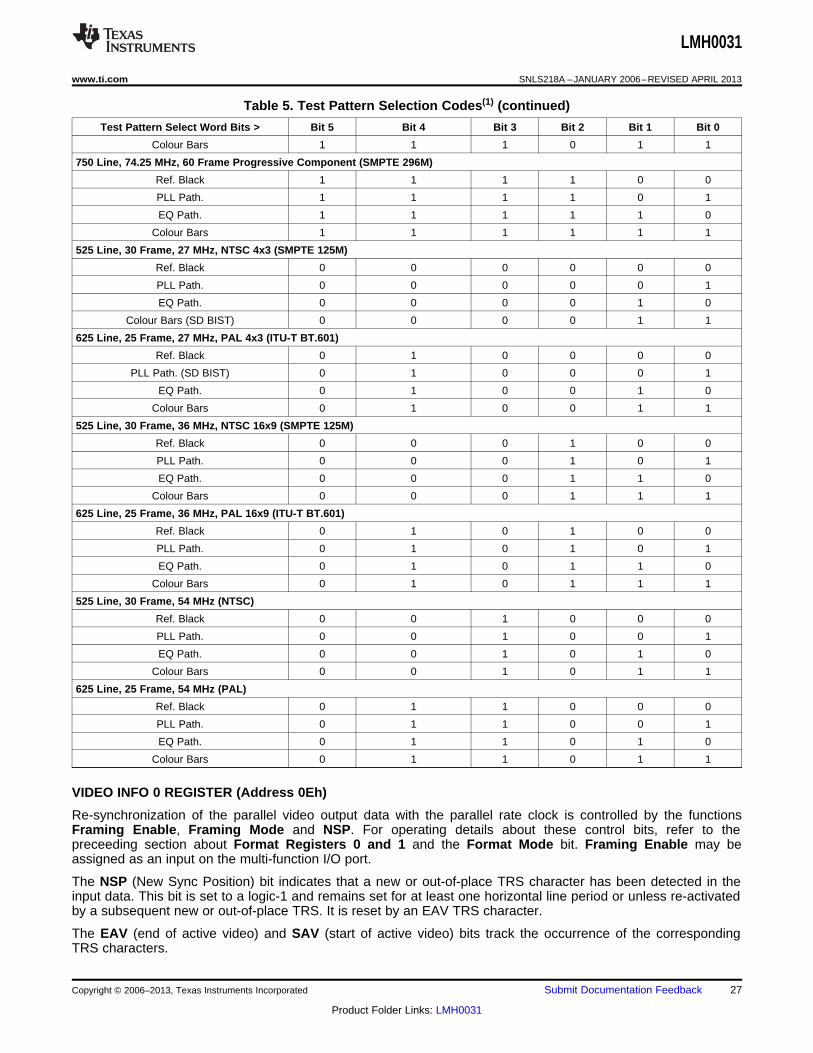
TEST 0 REGISTER (Address 0Dh)
The Test Pattern Select bits determine which test pattern is output when the Test Pattern Generator (TPG)mode or the Built-in Self-Test (BIST) mode is enabled. Table 5 gives the codes corresponding to the various testpatterns. All HD colour bar test patterns are inherently BIST data. BIST test patterns for SD are: NTSC, 27MHz,4x3 Colour Bars and PAL, 27MHz, 4x3 PLL Pathological.
The TPG Enable bit when set to a logic-1 enables the Test Pattern Generator function and built-in self-test(BIST).
The Pass/Fail bit indicates the result of the built-in self-test. This bit is a logic-1 for a pass condition.
Table 5. Test Pattern Selection Codes (1)
Test Pattern Select Word Bits > Bit 5 Bit 4 Bit 3 Bit 2 Bit 1 Bit 0
1=HD 1=Progressive 00=Black0=Interlaced 01=PLL Path.
Video Raster Standard0=SD 1=PAL 10=EQ Path.
0=NTSC 11=Colour Bars
1125 Line, 74.25 MHz, 30 Frame Interlaced Component (SMPTE 260M)
Ref. Black 1 0 0 0 0 0
PLL Path. 1 0 0 0 0 1
EQ Path. 1 0 0 0 1 0
Colour Bars 1 0 0 0 1 1
1125 Line, 74.25 MHz, 30 Frame Interlaced Component (SMPTE 274M)
Ref. Black 1 0 0 1 0 0
PLL Path. 1 0 0 1 0 1
EQ Path. 1 0 0 1 1 0
Colour Bars 1 0 0 1 1 1
1125 Line, 74.25 MHz, 25 Frame Interlaced Component (SMPTE 274M)
Ref. Black 1 0 1 0 0 0
PLL Path. 1 0 1 0 0 1
EQ Path. 1 0 1 0 1 0
Colour Bars 1 0 1 0 1 1
1125 Line, 74.25 MHz, 25 Frame Interlaced Component (SMPTE 295M)
Ref. Black 1 0 1 1 0 0
PLL Path. 1 0 1 1 0 1
EQ Path. 1 0 1 1 1 0
Colour Bars 1 0 1 1 1 1
1125 Line, 74.25 MHz, 30 Frame Progressive Component (SMPTE 274M)
Ref. Black 1 1 0 0 0 0
PLL Path. 1 1 0 0 0 1
EQ Path. 1 1 0 0 1 0
Colour Bars 1 1 0 0 1 1
1125 Line, 74.25 MHz, 25 Frame Progressive Component (SMPTE 274M)
Ref. Black 1 1 0 1 0 0
PLL Path. 1 1 0 1 0 1
EQ Path. 1 1 0 1 1 0
Colour Bars 1 1 0 1 1 1
1125 Line, 74.25 MHz, 24 Frame Progressive Component (SMPTE 274M)
Ref. Black 1 1 1 0 0 0
PLL Path. 1 1 1 0 0 1
EQ Path. 1 1 1 0 1 0
(1) Note: BIST test patterns for SD are: NTSC 4x3 Colour Bars and PAL 4x3 PLL Pathological.
26 Submit Documentation Feedback Copyright © 2006–2013, Texas Instruments Incorporated
Product Folder Links: LMH0031
LMH0031
www.ti.com SNLS218A –JANUARY 2006–REVISED APRIL 2013
Table 5. Test Pattern Selection Codes(1) (continued)
Test Pattern Select Word Bits > Bit 5 Bit 4 Bit 3 Bit 2 Bit 1 Bit 0
Colour Bars 1 1 1 0 1 1
750 Line, 74.25 MHz, 60 Frame Progressive Component (SMPTE 296M)
Ref. Black 1 1 1 1 0 0
PLL Path. 1 1 1 1 0 1
EQ Path. 1 1 1 1 1 0
Colour Bars 1 1 1 1 1 1
525 Line, 30 Frame, 27 MHz, NTSC 4x3 (SMPTE 125M)
Ref. Black 0 0 0 0 0 0
PLL Path. 0 0 0 0 0 1
EQ Path. 0 0 0 0 1 0
Colour Bars (SD BIST) 0 0 0 0 1 1
625 Line, 25 Frame, 27 MHz, PAL 4x3 (ITU-T BT.601)
Ref. Black 0 1 0 0 0 0
PLL Path. (SD BIST) 0 1 0 0 0 1
EQ Path. 0 1 0 0 1 0
Colour Bars 0 1 0 0 1 1
525 Line, 30 Frame, 36 MHz, NTSC 16x9 (SMPTE 125M)
Ref. Black 0 0 0 1 0 0
PLL Path. 0 0 0 1 0 1
EQ Path. 0 0 0 1 1 0
Colour Bars 0 0 0 1 1 1
625 Line, 25 Frame, 36 MHz, PAL 16x9 (ITU-T BT.601)
Ref. Black 0 1 0 1 0 0
PLL Path. 0 1 0 1 0 1
EQ Path. 0 1 0 1 1 0
Colour Bars 0 1 0 1 1 1
525 Line, 30 Frame, 54 MHz (NTSC)
Ref. Black 0 0 1 0 0 0
PLL Path. 0 0 1 0 0 1
EQ Path. 0 0 1 0 1 0
Colour Bars 0 0 1 0 1 1
625 Line, 25 Frame, 54 MHz (PAL)
Ref. Black 0 1 1 0 0 0
PLL Path. 0 1 1 0 0 1
EQ Path. 0 1 1 0 1 0
Colour Bars 0 1 1 0 1 1
VIDEO INFO 0 REGISTER (Address 0Eh)
Re-synchronization of the parallel video output data with the parallel rate clock is controlled by the functionsFraming Enable, Framing Mode and NSP. For operating details about these control bits, refer to thepreceeding section about Format Registers 0 and 1 and the Format Mode bit. Framing Enable may beassigned as an input on the multi-function I/O port.
The NSP (New Sync Position) bit indicates that a new or out-of-place TRS character has been detected in theinput data. This bit is set to a logic-1 and remains set for at least one horizontal line period or unless re-activatedby a subsequent new or out-of-place TRS. It is reset by an EAV TRS character.
The EAV (end of active video) and SAV (start of active video) bits track the occurrence of the correspondingTRS characters.
Copyright © 2006–2013, Texas Instruments Incorporated Submit Documentation Feedback 27
Product Folder Links: LMH0031

LMH0031
SNLS218A –JANUARY 2006–REVISED APRIL 2013 www.ti.com
The Lock Detect is a logic-1 when the loop is locked and the CDR has acquired a phase of the incoming serialdata. This bit may be programmed as an output on the multi-function I/O bus. This bit is mapped to I/O port bit 4in the default condition.
The VPG Filter Enable bit when set enables operation of the Video Pattern Generator filter. Operation of thisfilter causes the insertion of transition codes in the chroma and luma data of colour bar test patterns where thesepatterns change from one bar to the next. This filter reduces the magnitude of out-of-band frequency productswhich are produced by abrupt transitions in the chroma and luma data when fed to D-to-A converters and picturemonitors.
The LMH0031 incorporates circuitry that implements a method for handling data that has been subjected to LSBdithering. Data from the de-scrambler is routed for de-dithering. Control of this circuitry is via the De-DitherEnable bit in the VIDEO INFO 0 control register. Recovery of data that has been dithered during the verticalblanking interval can be selectively enabled by use of the V De-Dither Enable bit in the VIDEO INFO 0 controlregister. The initial condition of De-Dither Enable and V De-Dither Enable is OFF.
VIDEO CONTROL 0 (register address 55h)
The EXTERNAL VCLK bit is a special application function which enables use of an external VCXO as a substitutefor the internally generated VCLK. Additional circuitry is enabled within the LMH0031 which provides phase-frequency detection and control voltage output for the VCXO. An external loop filter and voltage amplifier arerequired to interface the control voltage output to the VCXO frequency control input. When this function is used,the RBB output function is changed from the bias supply output to the control voltage output of the phase-frequency detector. The VCLK output changes function, becoming the input for the VCXO signal. Use of thisfunction and required external support circuitry is explained in the Application Information section.
The SYNC DETECT ENABLE bit, when set, enables detection of TRS characters. This bit is normally set (ON).
The LSB CLIP ENABLE bit, when set, causes the two LSBs of TRS characters to be set to 00b as described inITU-R BT.601. This function is normally set (ON).
The NRZI ENABLE bit, when set, enables data to be converted from NRZI to NRZ. This bit is normally set (ON).
The DE-SCRAMBLE ENABLE bit, when set, enables de-scrambling of the incoming data according torequirements of SMPTE 259M or SMPTE 292M. This bit is normally set (ON).
CAUTION
The default state of this register is 36h. If any of the normal operating features of thedescrambler are turned off, this register’s default data must be restored to resumenormal device operation.
REFERENCE CLOCK REGISTER (Address 67h)
The Reference Clock register controls operation of the CDR reference clock source. The CLKEN bit when resetto a logic-0 enables the oscillator signal to be used by the LMH0031 as a reference. The default state of this bitat power-on is enabled. In general, this function and bit should not be disabled. The INT_OSC EN bit enables theinternal crystal oscillator amplifier. By default this bit is a logic-0 and is therefore inactive at power-on. The deviceexpects an external 27MHz reference reference clock source to be connected to the XTALi/Ext Clk pin andactivated at power-on.
I/O PIN 0 THROUGH 7 CONFIGURATION REGISTERS (Addresses 0Fh through 16h)
The I/O Pin Configuration Registers are used to map individual bits of the multi-function I/O port to selectedbits of the Configuration and Control Registers. Table 6 gives the pin select codes for the Configuration andControl register functions that may be mapped to the port. Pin[n] Select [5] controls whether the port pin is inputor output. The port pin will be an input when this bit is set and an output when reset. Input-only functions may notbe configured as outputs and vice versa. The remaining five Pin[n] Select [4:0] bits identify the particular ControlRegister bit to be mapped.
28 Submit Documentation Feedback Copyright © 2006–2013, Texas Instruments Incorporated
Product Folder Links: LMH0031

LMH0031
www.ti.com SNLS218A –JANUARY 2006–REVISED APRIL 2013
Example: Program, via the AD port, I/O port bit 0 as output for the CRC Luma Error bit in the control registers.1. Set ANC/CTRL to a logic-low.2. Set RD/WR to a logic-low.3. Present 00Fh to AD[9:0] as the I/O PIN 0 CONFIG register address.4. Toggle ACLK.5. Present 310h to AD[9:0] as the register data, the bit address of the CRC Luma Error bit in the control
registers.6. Toggle ACLK.
Table 6. Control Register Bit, Pin[n] SEL[5:0] Codes for I/O Port Pin Mapping (1)
Pin[n] SEL[5:0] Codes I/P orRegister Bit Power-On StatusO/P[5] [4] [3] [2] [1] [0] HEX
reserved 0 0 0 0 0 0 00 O/P
FF Flag Error 0 0 0 0 0 1 01 O/P
AP Flag Error 0 0 0 0 1 0 02 O/P
ANC Flag Error 0 0 0 0 1 1 03 O/P
CRC Error (SD/HD) 0 0 0 1 0 0 04 O/P I/O Port Bit 5
Addresses 05h and 06h are reserved
ANC FIFO 90% FULL 0 0 0 1 1 1 07 O/P
SHORT MSG DETECT 0 0 1 0 0 0 08 O/P
FULL MSG AVAIL 0 0 1 0 0 1 09 O/P
Addresses 0Ah through 0Ch are reserved
SAV 0 0 1 1 0 1 0D O/P
EAV 0 0 1 1 1 0 0E O/P I/O Port Bit 7
NSP 0 0 1 1 1 1 0F O/P
CRC Luma Error 0 1 0 0 0 0 10 O/P
CRC Chroma Error 0 1 0 0 0 1 11 O/P
F 0 1 0 0 1 0 12 O/P I/O Port Bit 0
V 0 1 0 0 1 1 13 O/P I/O Port Bit 1
H 0 1 0 1 0 0 14 O/P I/O Port Bit 2
Format[0] 0 1 0 1 0 1 15 O/P
Format[1] 0 1 0 1 1 0 16 O/P
Format[2] 0 1 0 1 1 1 17 O/P
Format[3] 0 1 1 0 0 0 18 O/P
Format[4] 0 1 1 0 0 1 19 O/P I/O Port Bit 3 (SD/HD)
FIFO Full 0 1 1 0 1 0 1A O/P
FIFO Empty 0 1 1 0 1 1 1B O/P I/O Port Bit 6
Lock Detect 0 1 1 1 0 0 1C O/P I/O Port Bit 4
Pass/Fail 0 1 1 1 0 1 1D O/P
FIFO Overrun 0 1 1 1 1 0 1E O/P
ANC Chksum Error 0 1 1 1 1 1 1F O/P
EDH Force 1 0 0 0 0 0 20 I/P
Test Pattern Select[0] 1 0 0 0 0 1 21 I/P
Test Pattern Select[1] 1 0 0 0 1 0 22 I/P
Test Pattern Select[2] 1 0 0 0 1 1 23 I/P
Test Pattern Select[3] 1 0 0 1 0 0 24 I/P
Test Pattern Select[4] 1 0 0 1 0 1 25 I/P
Test Pattern Select[5] 1 0 0 1 1 0 26 I/P
(1) Note: All LVCMOS inputs have internal pull-down devices except VCLK and ACLK.
Copyright © 2006–2013, Texas Instruments Incorporated Submit Documentation Feedback 29
Product Folder Links: LMH0031

LMH0031
SNLS218A –JANUARY 2006–REVISED APRIL 2013 www.ti.com
Table 6. Control Register Bit, Pin[n] SEL[5:0] Codes for I/O Port Pin Mapping(1) (continued)
Pin[n] SEL[5:0] Codes I/P orRegister Bit Power-On StatusO/P[5] [4] [3] [2] [1] [0] HEX
EDH Enable 1 0 0 1 1 1 27 I/P
TPG Enable 1 0 1 0 0 0 28 I/P
Addresses 29h through 2Bh are reserved
VPG Filter Enable 1 0 1 1 0 0 2C I/P
De-Dither Enable 1 0 1 1 0 1 2D I/P
Framing Enable 1 0 1 1 1 0 2E I/P
FIFO Extract Enable 1 0 1 1 1 1 2F I/P
PIN DESCRIPTIONSPin Name Description
1 AD9 Ancillary Data Output, Control Data Input
2 AD8 Ancillary Data Output, Control Data Input
3 AD7 Ancillary Data Output, Control Data Input
4 AD6 Ancillary Data Output, Control Data Input
5 AD5 Ancillary Data Output, Control Data Input
6 VSSD Negative Power Supply Input (2.5V supply, Digital Logic)
7 AD4 Ancillary Data Output, Control Data Input
8 AD3 Ancillary Data Output, Control Data Input
9 AD2 Ancillary Data Output, Control Data Input
10 AD1 Ancillary Data Output, Control Data Input
11 AD0 Ancillary Data Output, Control Data Input
12 VDDD Positive Power Supply Input (2.5V supply, Digital Logic)
13 ACLK ancillary/Control Clock Input
14 IO7 Multi-Function I/O Port
15 IO6 Multi-Function I/O Port
16 IO5 Multi-Function I/O Port
17 IO4 Multi-Function I/O Port
18 IO3 Multi-Function I/O Port
19 IO2 Multi-Function I/O Port
20 VSSIO Negative Power Supply Input (3.3V supply, I/O)
21 DV19 Parallel Video Output (HD=Luma)
22 DV18 Parallel Video Output (HD=Luma)
23 DV17 Parallel Video Output (HD=Luma)
24 DV16 Parallel Video Output (HD=Luma)
25 DV15 Parallel Video Output (HD=Luma)
26 VDDIO Positive Power Supply Input (3.3V supply, I/O)
27 DV14 Parallel Video Output (HD=Luma)
28 DV13 Parallel Video Output (HD=Luma)
29 DV12 Parallel Video Output (HD=Luma)
30 DV11 Parallel Video Output (HD=Luma)
31 DV10 Parallel Video Output (HD=Luma)
32 VSSD Negative Power Supply Input (2.5V supply, Digital Logic)
33 VDDD Positive Power Supply Input (2.5V supply, Digital Logic)
34 DV9 Parallel Video Output (HD=Chroma, SD=Luma & Chroma)
35 DV8 Parallel Video Output (HD=Chroma, SD=Luma & Chroma)
36 DV7 Parallel Video Output (HD=Chroma, SD=Luma & Chroma)
30 Submit Documentation Feedback Copyright © 2006–2013, Texas Instruments Incorporated
Product Folder Links: LMH0031

LMH0031
www.ti.com SNLS218A –JANUARY 2006–REVISED APRIL 2013
PIN DESCRIPTIONS (continued)
Pin Name Description
37 DV6 Parallel Video Output (HD=Chroma, SD=Luma & Chroma)
38 DV5 Parallel Video Output (HD=Chroma, SD=Luma & Chroma)
39 VSSD Negative Power Supply Input (2.5V supply, Digital Logic)
40 DV4 Parallel Video Output (HD=Chroma, SD=Luma & Chroma)
41 DV3 Parallel Video Output (HD=Chroma, SD=Luma & Chroma)
42 DV2 Parallel Video Output (HD=Chroma, SD=Luma & Chroma)
43 DV1 Parallel Video Output (HD=Chroma, SD=Luma & Chroma)
44 DV0 Parallel Video Output (HD=Chroma, SD=Luma & Chroma)
45 IO1 Multi-Function I/O Port
46 IO0 Multi-Function I/O Port
47 VSSIO Negative Power Supply Input (3.3V supply, I/O)
48 VDDIO Positive Power Supply Input (3.3V supply, I/O)
49 RESET Manual Reset Input (High True)
50 VCLK Parallel Video Data Clock Output
51 VDDPLL Positive Power Supply Input (2.5V supply, PLL)
52 VSSPLL Negative Power Supply Input (2.5V supply, PLL)
53 RREF Current Reference Resistor
54 RBB SDI Bias Supply Resistor
55 VSSSI Negative Power Supply Input (3.3V supply, Serial Input)
56 SDI Serial Data Complement Input
57 SDI Serial Data True Input
58 VDDSI Positive Power Supply Input (3.3V supply, Serial Input)
59 VSSIO Negative Power Supply Input (3.3V supply, I/O)
60 XTALi/EXT CLK Crystal or External 27MHz Clock Input
61 XTALo Crystal (Oscillator Output)
62 VDDD Positive Power Supply Input (2.5V supply, Digital Logic)
63 ANC/CTRL ancillary/Control Data Port Function Control Input
64 RD/WR ancillary/Control Data Port Read/Write Control Input
Copyright © 2006–2013, Texas Instruments Incorporated Submit Documentation Feedback 31
Product Folder Links: LMH0031

LMH0031
SNLS218A –JANUARY 2006–REVISED APRIL 2013 www.ti.com
Application Information
A typical application circuit for the LMH0031 is shown in the Application Circuit diagram. This circuitdemonstrates the capabilities of the LMH0031 and allows its evaluation in a native configuration. An assembleddemonstration board is available, part number SD131EVK. The board may be ordered through any of TI's salesoffices. Complete circuit board layouts and schematics for the SD131EVK are available on TI's WEB site. Forlatest availability information, please see: www.ti.com/appinfo/interface.
PCB LAYOUT AND POWER SYSTEM BYPASS RECOMMENDATIONS
Circuit board layout and stack-up for the LMH0031 should be designed to provide noise-free power to the device.Good layout practice also will separate high frequency or high-level inputs and outputs from low-level inputs tominimize unwanted stray noise pickup, feedback and interference. Power system performance may be greatlyimproved by using thin dielectrics (4 to 10 mils) for power/ground sandwiches. This increases the intrinsiccapacitance of the PCB power system which improves power supply filtering, especially at high frequencies, andmakes the value and placement of external bypass capacitors less critical. External bypass capacitors shouldinclude both RF ceramic and tantalum electrolytic types. RF capacitors may use values in the range 0.01 µF to0.1 µF. Tantalum capacitors may be in the range 2.2 µF to 10 µF. Voltage rating for tantalum capacitors shouldbe at least 5X the power supply voltage being used. It is recommended practice to use two vias at each powerpin of the LMH0031 as well as all RF bypass capacitor terminals. Dual vias reduce the interconnect inductanceby up to half, thereby extending the effective frequency range of the bypass components.
The outer layers of the PCB may be flooded with additional VSS (ground) plane. These planes will improveshielding and isolation as well as increase the intrinsic capacitance of the power supply plane system. Naturally,to be effective, these planes must be tied to the VSS power supply plane at frequent intervals with vias. Frequentvia placement also improves signal integrity on signal transmission lines by providing short paths for imagecurrents which reduces signal distortion. The planes should be pulled back from all transmission lines andcomponent mounting pads a distance equal to the width of the widest transmission line or the thickness of thedielectric separating the transmission line from the internal power or ground plane(s) whichever is greater. Doingso minimizes effects on transmission line impedances and reduces unwanted parasitic capacitances atcomponent mounting pads.
In especially noisy power supply environments, such as is often the case when using switching power supplies,separate filtering may be used at the LMH0031's PLL and serial input power pins. The LMH0031 was designedfor this situation. The I/O, digital section, PLL and serial input power supply feeds are independent (see table andBlock Diagram for details). Supply filtering may take the form of L-section or pi-section, L-C filters in series withthese VDD inputs. Such filters are available in a single package from several manufacturers. Device powersupplies must be either sequenced as described in POWER SUPPLIES, POWER-ON-RESET AND RESETINPUT and ideally should be applied simultaneously as from a common source.
MAINTAINING OUTPUT DATA INTEGRITY
The way in which the TRS and other video data characters are specified and are therefore output in parallel formcan result in the simultaneous switching of many of the LMH0031’s CMOS outputs. Such switching can lead tothe production of output high level droop or low level ground bounce. Given in the specifications, VOLP is the peakoutput LOW voltage or ground bounce and VOHV is the lowest output HIGH voltage or output droop that mayoccur under dynamic simultaneous output switching conditions. VOHV and VOLP are measured with respect toreference ground. Careful attention to PCB layout, power pin connections to the power planes and timing of theoutput data clocking can reduce these effects. Consideration must also be given to the timing allocated toexternal circuits which sample the outputs.
The effects of simultaneous output switching on output levels may be minimized by adopting good PCB layoutand data output timing practices, especially critical at HD data rates. The power pins feeding the I/O should havelow inductance connections to the power and ground planes. It is recommended that these connections use atleast two vias per power or ground pin. Short interconnecting traces consistent with good layout practices andsoldering rules must be used. Sampling or clocking of data by external devices should be so timed as to takemaximum advantage of the steady-state portion of the parallel output data interval. The LMH0031 is designed sothat video data will be stable at the positive-going transition of VCLK. Data should not be sampled close to thedata transition intervals associated with the negative-going clock edge. The specified propagation delay andclock to data timing parameters must be observed. When data is being sampled from the video data porttogether with the ANC port and/or I/O port, it is recommended that the sampling clocks be synchronized with thevideo clock, VCLK, to minimize possible effects from ground bounce or output droop on sampled signal levels.
32 Submit Documentation Feedback Copyright © 2006–2013, Texas Instruments Incorporated
Product Folder Links: LMH0031

LMH0031
www.ti.com SNLS218A –JANUARY 2006–REVISED APRIL 2013
PROCESSING NON-SUPPORTED RASTER FORMATS
The number and type of HD raster formats has proliferated since the LMH0031 was designed. Though notspecifically capable of fully or automatically processing these new formats, the LMH0031 may still be capable ofdeserializing them. The user is encouraged to experiment with processing these formats, keeping in mind thatthe LMH0031 has not been tested to handle formats other than those detailed in Table 4. Therefore, the resultsfrom attempts to process non-supported formats is not ensured. The following guidelines concerning devicesetup are provided to aid the user in configuring the LMH0031 to attempt limited processing of these other rasterformats.
In general, the device is configured to defeat its automatic format detection function and to limit operation to ageneral HD format. (The user should consult Table 4 for guidance on the format groups similar to the non-supported one to be processed). Since most non-supported formats are in the HD group, the LMH0031 shouldbe configured to operate in HD-ONLY mode by setting bit-5 of the FORMAT 0 register (address 0Bh). Also, thedevice should be further configured by loading the FORMAT SET[4:0] bits of this register with the general HDsub-format code. In addition, since control data is being written to the port, AD[9:8] must be driven as 11b. Thecomplete data word for this general HD sub-format code with HD-ONLY bit set is 33Fh. Since this format differsfrom those in the table, the EAV/SAV indicators are disabled. Without these indicators, line numbering and CRCprocessing are disabled and ANC data extraction will not function. Output video chroma and luma data will beword-aligned. Post-processing of the parallel data output from the LMH0031 will be needed to implement CRCchecking or line number tracking.
USING EXTERNAL VCXO FOR VCLK
The EXTERNAL VCLK bit of VIDEO CONTROL 0 (register address 55h) is a special application function whichenables use of an external VCXO as a substitute for the internally generated VCLK. Additional circuitry is enabledwithin the LMH0031 which provides phase-frequency detection and control voltage output for the VCXO. Anexternal loop filter and voltage amplifier are required to interface the control voltage output to the VCXOfrequency control input. When this function is used, the RBB output function is changed from the bias supplyoutput to the control voltage output of the phase-frequency detector. The VCLK output changes function,becoming the input for the VCXO signal.
Figure 8 shows an example using dual VCXOs for VCLK to handle both standard and high definition video.
Copyright © 2006–2013, Texas Instruments Incorporated Submit Documentation Feedback 33
Product Folder Links: LMH0031

+
-
100 k:
182 k:
VCTRL FOUT
LMC7101
+3.3V
VCTRL FOUT
+3.3V
NC7SZ126
74.25 MHzVCXO
27.00 MHzVCXO
LMH0031
RB B
RREF
VCLK
22.1 k:100 pF
10 nF4.75 k:
DV[19:0]
To other logic or
serializer
CAUTION! Read text before using this
circuit.
NC7SZ125
NC7SZ08
CLC031 IO3 - SD/HD
CLC031 IO4 - Lock Detect
OE
OE
22.1:
22.1:
LMH0031
SNLS218A –JANUARY 2006–REVISED APRIL 2013 www.ti.com
Figure 8. Using Dual VCXOs for VCLK Example
The control voltage output from RBB is externally filtered by the loop filter consisting of a 22.1kΩ resistor in serieswith a 10nF capacitor, combined in parallel with a 100pF capacitor. This gives a loop bandwidth of 1.5kHz. Sincethe control voltage is limited to around 2.1V, it requires a level shifter to get the entire pull range on the VCXO.TI's LMC7101 is recommended with 100kΩ and 182kΩ resistors as shown in Figure 8 to provide a gain of 1.55,sufficient to drive a 3.3V VCXO.
Recommended VCXOs from SaRonix (141 Jefferson Drive, Menlo Park, CA 94025, USA) include theST1308AAB-74.25 for high definition and the ST1307BAB-27.00 for standard definition. Dual VCXOs requiresome supporting logic to select the appropriate VCXO. This requires the use of Format[4] (SD/HD) and LockDetect, which are mapped at power-on to I/O Port Bit 3 and I/O Port Bit 4, respectively. These two signals passthrough an AND gate (Fairchild Semiconductor's NC7SZ08 or similar). Its output is high when both Lock Detectand Format[4] are high, which indicates a valid high-definition signal is present. The VCXOs are buffered tocontrol the transition times and to allow easy selection. The output of the AND gate is used to control the OutputEnable (OE) function of the buffers. The 74.25MHz VCXO is buffered with the NC7SZ126 with the AND gateoutput connected to the OE pin of the NC7SZ126, and the 27.00MHz VCXO is buffered with the NC7SZ125 withthe AND gate output connected to the OE pin of the NC7SZ125. This circuit uses the 27.00MHz VCXO asdefault and enables the 74.25MHz VCXO when a valid high-definition signal is present. The outputs from thebuffers are daisy-chained together and sent to the LMH0031's VCLK in addition to other devices, such as theLMH0030 serializer.
34 Submit Documentation Feedback Copyright © 2006–2013, Texas Instruments Incorporated
Product Folder Links: LMH0031

LMH0031
www.ti.com SNLS218A –JANUARY 2006–REVISED APRIL 2013
REVISION HISTORY
Changes from Original (April 2013) to Revision A Page
• Changed layout of National Data Sheet to TI format .......................................................................................................... 34
Copyright © 2006–2013, Texas Instruments Incorporated Submit Documentation Feedback 35
Product Folder Links: LMH0031

PACKAGE OPTION ADDENDUM
www.ti.com 24-Nov-2013
Addendum-Page 1
PACKAGING INFORMATION
Orderable Device Status(1)
Package Type PackageDrawing
Pins PackageQty
Eco Plan(2)
Lead/Ball Finish(6)
MSL Peak Temp(3)
Op Temp (°C) Device Marking(4/5)
Samples
LMH0031VS NRND TQFP PAG 64 160 TBD Call TI Call TI 0 to 70 L031
LMH0031VS/NOPB ACTIVE TQFP PAG 64 160 Green (RoHS& no Sb/Br)
CU SN Level-3-260C-168 HR 0 to 70 L031
(1) The marketing status values are defined as follows:ACTIVE: Product device recommended for new designs.LIFEBUY: TI has announced that the device will be discontinued, and a lifetime-buy period is in effect.NRND: Not recommended for new designs. Device is in production to support existing customers, but TI does not recommend using this part in a new design.PREVIEW: Device has been announced but is not in production. Samples may or may not be available.OBSOLETE: TI has discontinued the production of the device.
(2) Eco Plan - The planned eco-friendly classification: Pb-Free (RoHS), Pb-Free (RoHS Exempt), or Green (RoHS & no Sb/Br) - please check http://www.ti.com/productcontent for the latest availabilityinformation and additional product content details.TBD: The Pb-Free/Green conversion plan has not been defined.Pb-Free (RoHS): TI's terms "Lead-Free" or "Pb-Free" mean semiconductor products that are compatible with the current RoHS requirements for all 6 substances, including the requirement thatlead not exceed 0.1% by weight in homogeneous materials. Where designed to be soldered at high temperatures, TI Pb-Free products are suitable for use in specified lead-free processes.Pb-Free (RoHS Exempt): This component has a RoHS exemption for either 1) lead-based flip-chip solder bumps used between the die and package, or 2) lead-based die adhesive used betweenthe die and leadframe. The component is otherwise considered Pb-Free (RoHS compatible) as defined above.Green (RoHS & no Sb/Br): TI defines "Green" to mean Pb-Free (RoHS compatible), and free of Bromine (Br) and Antimony (Sb) based flame retardants (Br or Sb do not exceed 0.1% by weightin homogeneous material)
(3) MSL, Peak Temp. - The Moisture Sensitivity Level rating according to the JEDEC industry standard classifications, and peak solder temperature.
(4) There may be additional marking, which relates to the logo, the lot trace code information, or the environmental category on the device.
(5) Multiple Device Markings will be inside parentheses. Only one Device Marking contained in parentheses and separated by a "~" will appear on a device. If a line is indented then it is a continuationof the previous line and the two combined represent the entire Device Marking for that device.
(6) Lead/Ball Finish - Orderable Devices may have multiple material finish options. Finish options are separated by a vertical ruled line. Lead/Ball Finish values may wrap to two lines if the finishvalue exceeds the maximum column width.
Important Information and Disclaimer:The information provided on this page represents TI's knowledge and belief as of the date that it is provided. TI bases its knowledge and belief on informationprovided by third parties, and makes no representation or warranty as to the accuracy of such information. Efforts are underway to better integrate information from third parties. TI has taken andcontinues to take reasonable steps to provide representative and accurate information but may not have conducted destructive testing or chemical analysis on incoming materials and chemicals.TI and TI suppliers consider certain information to be proprietary, and thus CAS numbers and other limited information may not be available for release.

PACKAGE OPTION ADDENDUM
www.ti.com 24-Nov-2013
Addendum-Page 2
In no event shall TI's liability arising out of such information exceed the total purchase price of the TI part(s) at issue in this document sold by TI to Customer on an annual basis.

MECHANICAL DATA
MTQF006A – JANUARY 1995 – REVISED DECEMBER 1996
POST OFFICE BOX 655303 • DALLAS, TEXAS 75265
PAG (S-PQFP-G64) PLASTIC QUAD FLATPACK
0,13 NOM
0,25
0,450,75
Seating Plane
0,05 MIN
4040282/C 11/96
Gage Plane
33
0,170,27
16
48
1
7,50 TYP
49
64
SQ
9,80
1,050,95
11,8012,20
1,20 MAX
10,20SQ
17
32
0,08
0,50 M0,08
0°–7°
NOTES: A. All linear dimensions are in millimeters.B. This drawing is subject to change without notice.C. Falls within JEDEC MS-026

IMPORTANT NOTICE
Texas Instruments Incorporated and its subsidiaries (TI) reserve the right to make corrections, enhancements, improvements and otherchanges to its semiconductor products and services per JESD46, latest issue, and to discontinue any product or service per JESD48, latestissue. Buyers should obtain the latest relevant information before placing orders and should verify that such information is current andcomplete. All semiconductor products (also referred to herein as “components”) are sold subject to TI’s terms and conditions of salesupplied at the time of order acknowledgment.TI warrants performance of its components to the specifications applicable at the time of sale, in accordance with the warranty in TI’s termsand conditions of sale of semiconductor products. Testing and other quality control techniques are used to the extent TI deems necessaryto support this warranty. Except where mandated by applicable law, testing of all parameters of each component is not necessarilyperformed.TI assumes no liability for applications assistance or the design of Buyers’ products. Buyers are responsible for their products andapplications using TI components. To minimize the risks associated with Buyers’ products and applications, Buyers should provideadequate design and operating safeguards.TI does not warrant or represent that any license, either express or implied, is granted under any patent right, copyright, mask work right, orother intellectual property right relating to any combination, machine, or process in which TI components or services are used. Informationpublished by TI regarding third-party products or services does not constitute a license to use such products or services or a warranty orendorsement thereof. Use of such information may require a license from a third party under the patents or other intellectual property of thethird party, or a license from TI under the patents or other intellectual property of TI.Reproduction of significant portions of TI information in TI data books or data sheets is permissible only if reproduction is without alterationand is accompanied by all associated warranties, conditions, limitations, and notices. TI is not responsible or liable for such altereddocumentation. Information of third parties may be subject to additional restrictions.Resale of TI components or services with statements different from or beyond the parameters stated by TI for that component or servicevoids all express and any implied warranties for the associated TI component or service and is an unfair and deceptive business practice.TI is not responsible or liable for any such statements.Buyer acknowledges and agrees that it is solely responsible for compliance with all legal, regulatory and safety-related requirementsconcerning its products, and any use of TI components in its applications, notwithstanding any applications-related information or supportthat may be provided by TI. Buyer represents and agrees that it has all the necessary expertise to create and implement safeguards whichanticipate dangerous consequences of failures, monitor failures and their consequences, lessen the likelihood of failures that might causeharm and take appropriate remedial actions. Buyer will fully indemnify TI and its representatives against any damages arising out of the useof any TI components in safety-critical applications.In some cases, TI components may be promoted specifically to facilitate safety-related applications. With such components, TI’s goal is tohelp enable customers to design and create their own end-product solutions that meet applicable functional safety standards andrequirements. Nonetheless, such components are subject to these terms.No TI components are authorized for use in FDA Class III (or similar life-critical medical equipment) unless authorized officers of the partieshave executed a special agreement specifically governing such use.Only those TI components which TI has specifically designated as military grade or “enhanced plastic” are designed and intended for use inmilitary/aerospace applications or environments. Buyer acknowledges and agrees that any military or aerospace use of TI componentswhich have not been so designated is solely at the Buyer's risk, and that Buyer is solely responsible for compliance with all legal andregulatory requirements in connection with such use.TI has specifically designated certain components as meeting ISO/TS16949 requirements, mainly for automotive use. In any case of use ofnon-designated products, TI will not be responsible for any failure to meet ISO/TS16949.
Products ApplicationsAudio www.ti.com/audio Automotive and Transportation www.ti.com/automotiveAmplifiers amplifier.ti.com Communications and Telecom www.ti.com/communicationsData Converters dataconverter.ti.com Computers and Peripherals www.ti.com/computersDLP® Products www.dlp.com Consumer Electronics www.ti.com/consumer-appsDSP dsp.ti.com Energy and Lighting www.ti.com/energyClocks and Timers www.ti.com/clocks Industrial www.ti.com/industrialInterface interface.ti.com Medical www.ti.com/medicalLogic logic.ti.com Security www.ti.com/securityPower Mgmt power.ti.com Space, Avionics and Defense www.ti.com/space-avionics-defenseMicrocontrollers microcontroller.ti.com Video and Imaging www.ti.com/videoRFID www.ti-rfid.comOMAP Applications Processors www.ti.com/omap TI E2E Community e2e.ti.comWireless Connectivity www.ti.com/wirelessconnectivity
Mailing Address: Texas Instruments, Post Office Box 655303, Dallas, Texas 75265Copyright © 2016, Texas Instruments Incorporated


![MXC-FGX-TK1 Datasheet [rev 4] - csi.pl · 64 GB Embedded Flash n 2× HD‑SDI input (SMPTE‑292M) n 1× HD‑SDI output (SMPTE‑292M); Optionally can be mirrored to a second output](https://img.pdfslide.net/doc/110x75/5f588a1707951e41df314ddf/mxc-fgx-tk1-datasheet-rev-4-csipl-64-gb-embedded-flash-n-2-hdasdi-input.jpg)